

Page 1
Intelligent Double Low-Side Switch 2 x 0.5 A
Features
● Double low-side switch, 2 x 0.5 A
● Power limitation
● Overtemperature shutdown
● Overvoltage shutdown
● Status monitoring
● Shorted-load protection
● Integrated clamp diodes
● Temperature range – 40 to 125 °C
TLE 4214 G
Bipolar IC
P-DSO-20-7
Type Ordering Code Package
TLE 4214 G Q67000-A9094 P-DSO-20-7 (SMD)
Application
Applications in automotive electronics require intelligent power switches activated by
logic signals, which are shorted-load protected and provide error feedback.
This IC contains two of these power switches (low-side switches). In case of inductive
loads the integrated clamp diodes clamp the discharging voltage. If a “high” signal is
applied to the enable input both switches can be activated independently of one another
with TTL signals at the control inputs (active high). The high impedance inputs should
always be connected to a fixed potential (noise immunity).
The status output (open collector) signals the following malfunctions with high potential:
● Overload,
● Open load,
● Shorted load to ground,
● Overvoltage,
● Overtemperature.
Semiconductor Group 294 10.96
Page 2
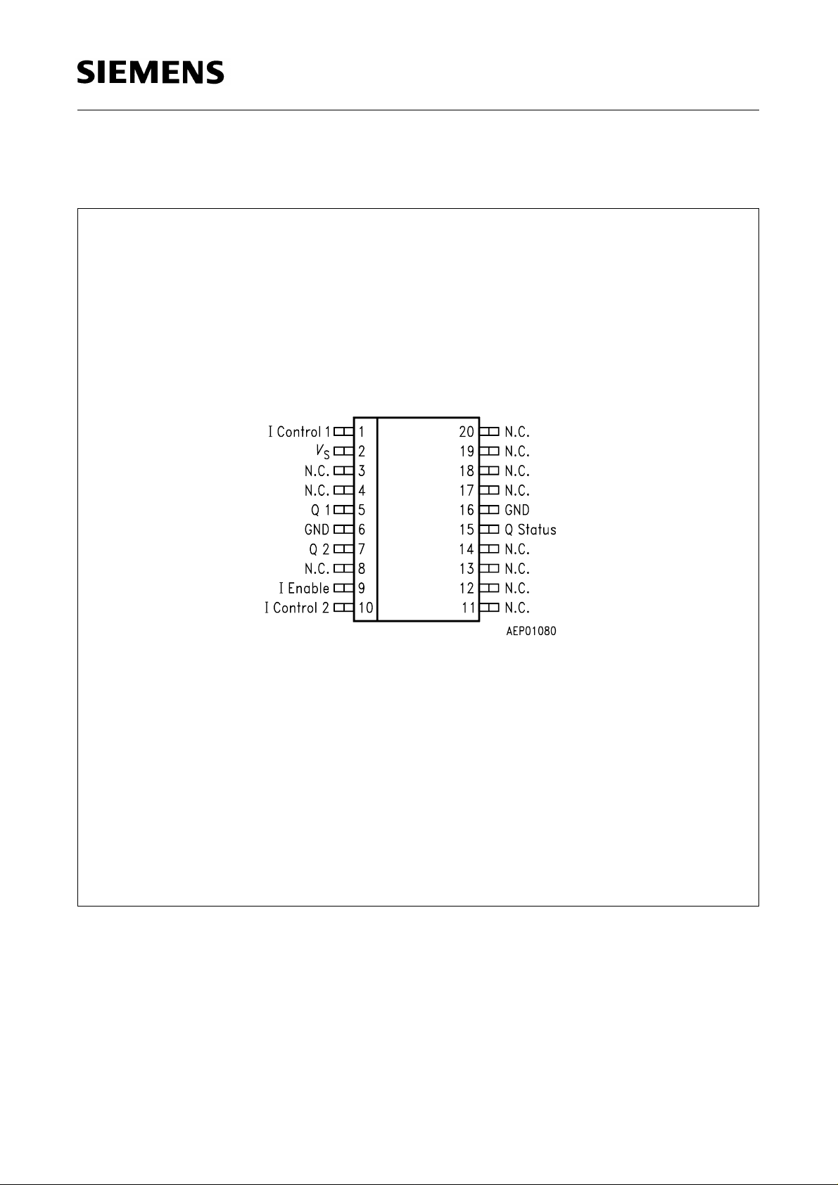
Pin Configuration
(top view)
TLE 4214 G
TLE 4214 G
Semiconductor Group 295
Page 3
TLE 4214 G
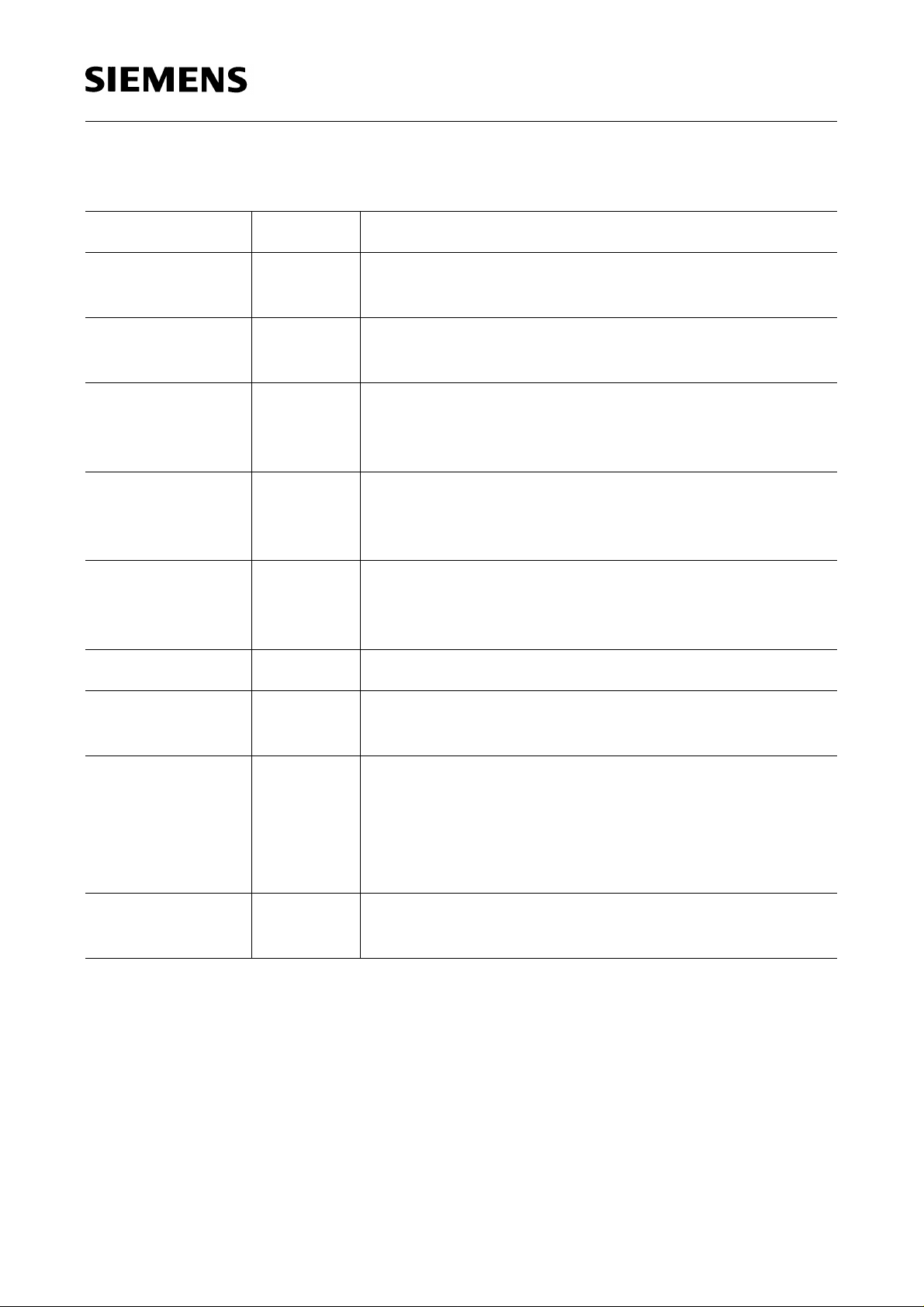
Pin Definitions and Functions
Pin No. Symbol Function
6, 16 GND Ground Design wiring for the max.
short-circuit current (2 x 1 A)
10 IN2 Control input 2 (TTL compatible) activates the output
transistor 2 in case of high potential
2
V
S
Supply voltageIn case of overvoltage at this pin large
sections of the circuit are deactivated. The status
output indicates this malfunction without delay time.
7Q2Output 2 Shorted load protected, open collector
output for currents up to 0.5 A, with clamping diodes to
supply voltage.
5Q1Output 1 Shorted load protected, open collector
output for currents up to 0.5 A, with clamping diodes to
supply voltage.
9 ENA Enable input, active high
1 IN1 Control input 1 (TTL-compatible) activates output
transistor 1 in case of high potential
15 STA Status output (open collector) for both outputs;
indicates overtemperature, overload, open load and
shorted load to ground as well as overvoltage at pin 3.
It is switched to high after a defined delay time in case
of malfunction (except: overvoltage)
3, 4, 8, 11 … 14,
N. C. Not connected
17…20
Semiconductor Group 296
Page 4
TLE 4214 G
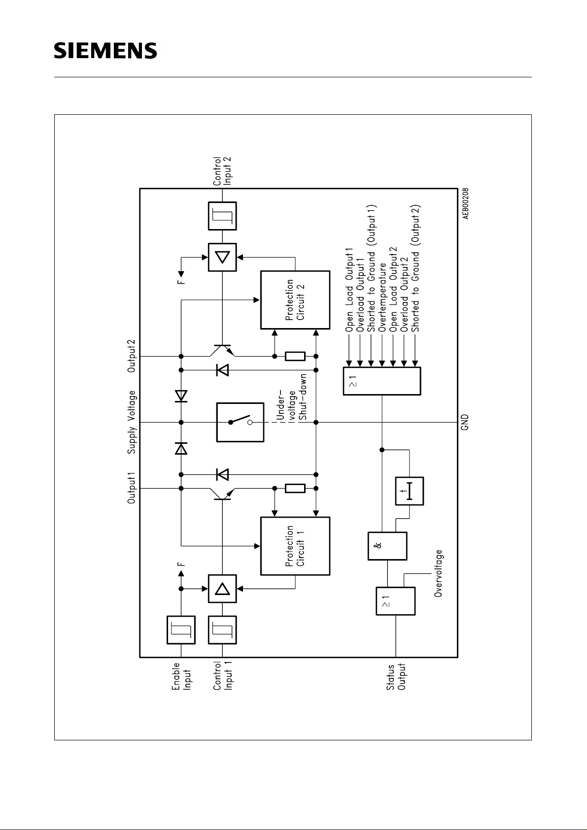
Block Diagram
Semiconductor Group 297
Page 5

TLE 4214 G
Circuit Description
Input Circuits
The control inputs and the enable input consist of TTL-compatible Schmitt triggers with
hysteresis. Controlled by these stages the buffer amplifiers drive the NPN power
transistors.
Switching Stages
The output stages consist of NPN power transistors with open collectors. Since the
protective circuit allocated to each stage limits the power dissipation, the outputs are
shorted-load protected to the supply voltage throughout the entire operating range.
Positive voltage peaks, which occur during the switching of inductive loads, are limited
by the integrated clamp diodes.
Monitoring and Protective Functions
During the activated status the outputs are monitored for open load, overload, and
shorted load to ground (see table below). In addition, large sections of the circuit are shut
down in case of excessive supply voltages
V
. Linked via OR gate the information
S
regarding these malfunctions effects the status output (open collector, active high). An
internally determined delay time applied to all malfunctions but overvoltage prevents the
output of messages in case of short-term malfunctions. Furthermore, a temperature
protection circuit prevents thermal overload. If overload occurs, the outputs are
protected according to the safe operating area (SOA) mode (see diagram). If voltage
and current are outside the SOA, the outputs oscillate to reduce the power dissipation.
The switching frequency depends on the internal delay time and the external load
(inductances and capacitances). If the frequency is low, the status output may follow the
oscillation. An integrated reverse diode protects the supply voltage
V
against reverse
S
polarities. Similarly the load circuit is protected against reverse polarities within the limits
established by the maximum ratings (no shorted load at the same time!). At supply
voltages below the operating range an undervoltage detector ensures that neither the
status nor the outputs are activated. At supply voltages below the operating range the
output stages are de-activated.
Semiconductor Group 298
Page 6
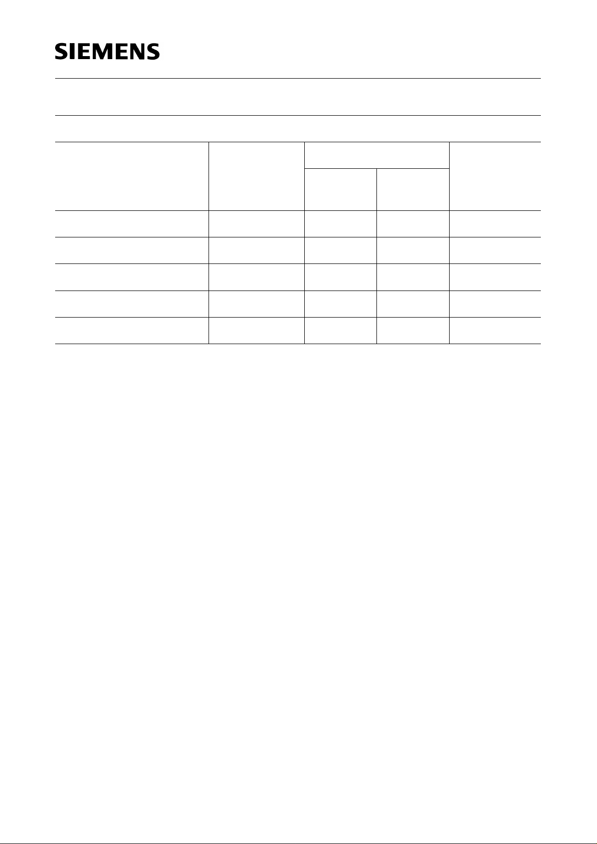
Status Output (H = Error)
TLE 4214 G
Undervoltage
Operating Range Overvoltage
> 3.5 V
V
= L
I
(passive)
V
= H
I
(active)
Normal function L L L H
Overload L L H H
Open load L L H H
Shorted output to ground L H H H
Overtemperature L H H H
Semiconductor Group 299
Page 7
TLE 4214 G
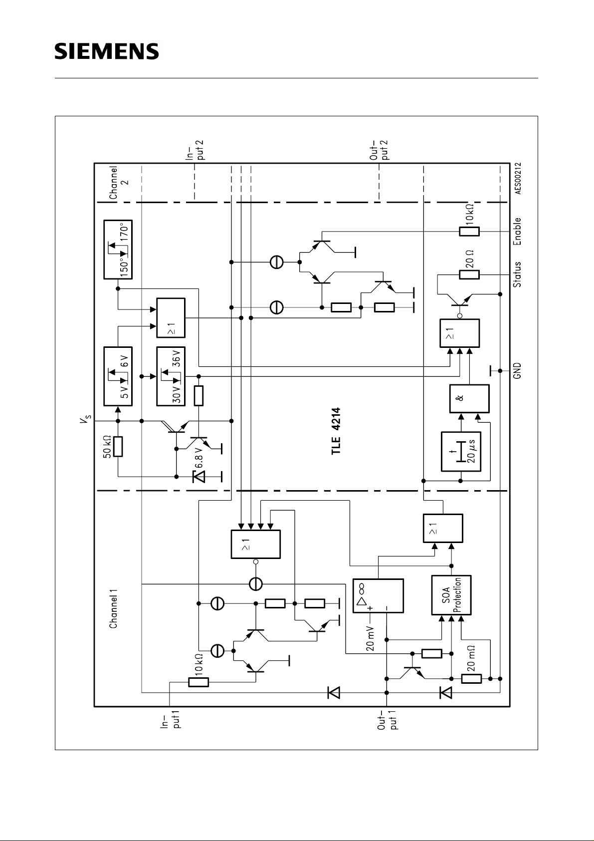
Circuit Diagram
Semiconductor Group 300
Page 8
TLE 4214 G
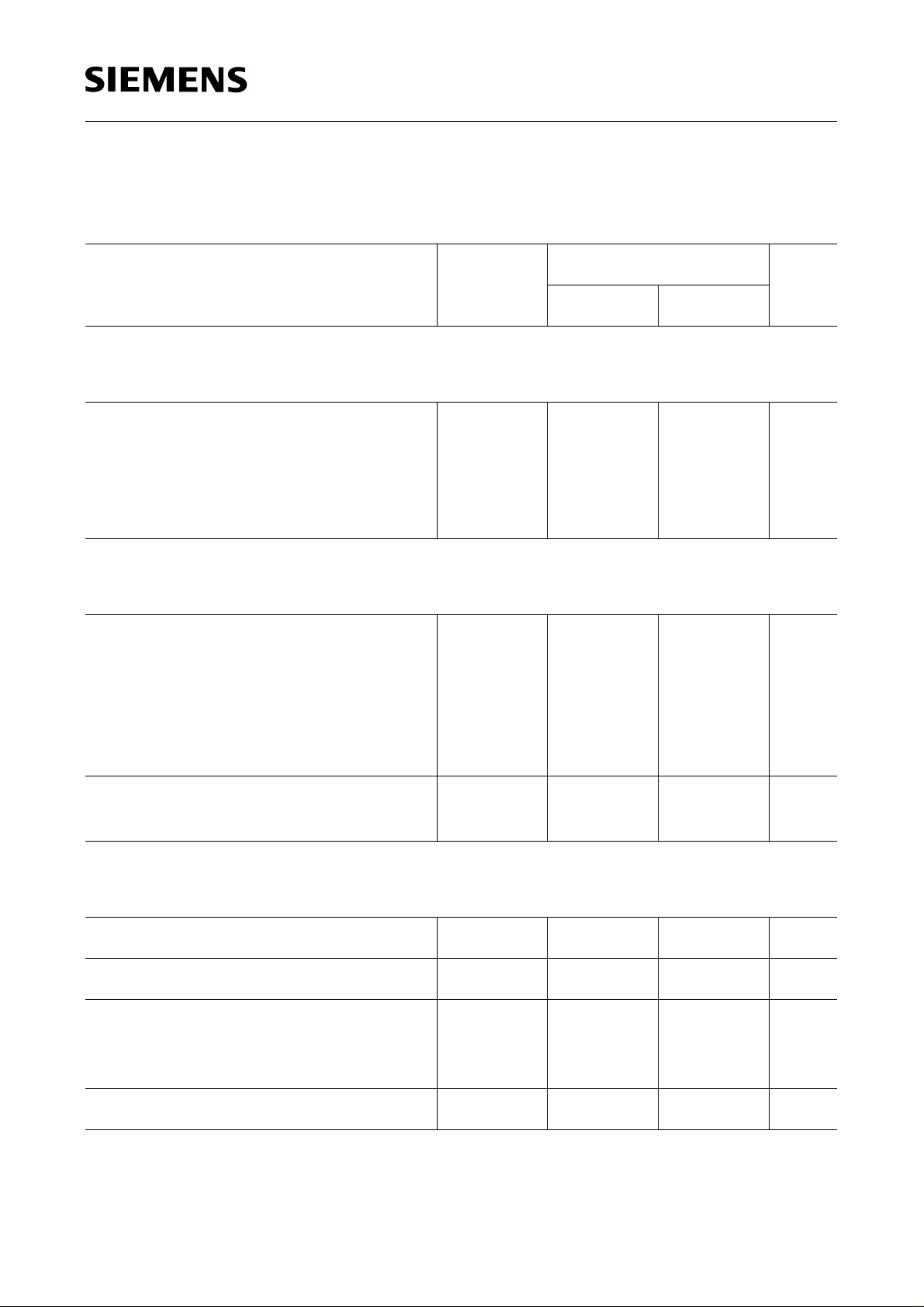
Absolute Maximum Ratings
T
= – 40 to 150 °C
j
Parameter Symbol Limit Values Unit
min. max.
Voltages
Supply voltage,
t < 0.2 s
Supply voltage
Input voltage
Output voltage (status output)
Output voltage (switching stages)
Currents
Output current (switching stages)
Current with reverse polarity,
t< 0.1 s
Output current positive clamp
Ground current
Output current (status output)
Junction temperature
Storage temperature
V
V
V
V
V
I
Q
I
Q
I
Q
I
GND
I
O
T
T
S
S
I
O
Q
j
stg
–
– 1.3
–13
– 0.3
– 0.3
internally
limited
– 0.7
–
– 1.4
–
–
– 50
70
40
40
40
+
V
–
–
0.7
2.0
10
150
150
V
V
V
V
S
V
–
A
A
A
mA
°C
°C
Operating Range
Supply voltage
Supply voltage slew rate d
Output current (switching stages)
Input voltage
Output current (status output)
Ambient temperature
1)
Lower limit = 5 V, if previously VS greater than 6 V (turn-on hysteresis)
Semiconductor Group 301
V
S
V
/dt – 1 1 V/µs
S
I
Q
V
, V
I
F
I
O
T
A
1)
6
– 0.5
– 5
0
25 V
0.5
32
5
A
V
mA
– 40 125 °C
Page 9
TLE 4214 G
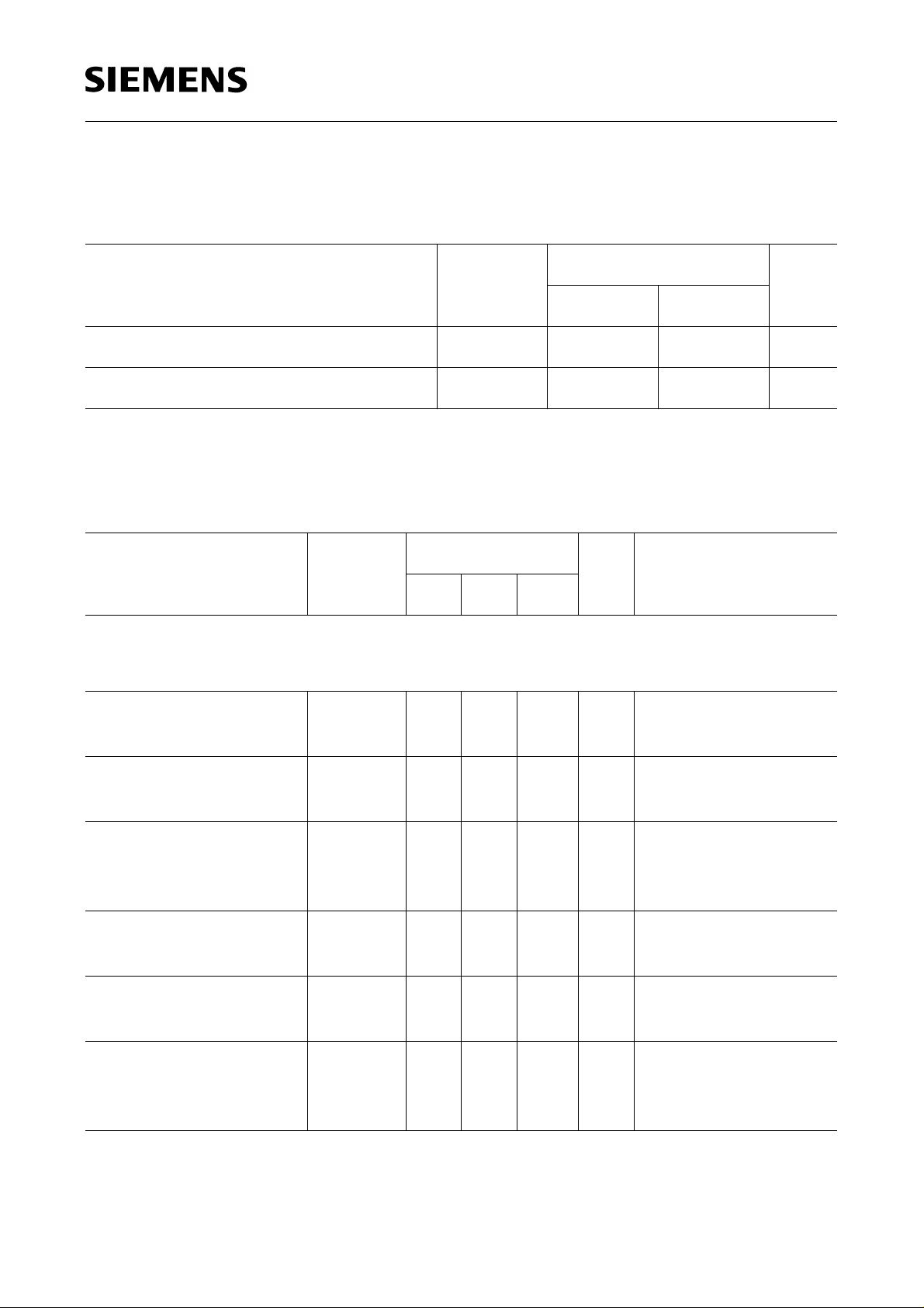
Absolute Maximum Ratings (cont’d)
T
= – 40 to 150 °C
j
Parameter Symbol Limit Values Unit
min. max.
Supply voltage while shorted load V
Thermal resistance junction to ambient
R
S
th JA
–15V
– 77 K/W
Characteristics
V
= 6 to 16 V (typ. VS = 12 V); Tj = – 40 to 150 °C (typ. Tj = 25 °C)
S
Parameter Symbol Limit Values Unit Test Condition
min. typ. max.
General Characteristics
Quiescent current
Supply voltage
Supply overvoltage
I
I
V
S
S
SO
–
–
30 37 42 V VL = 5 V; VO > 4.5 V
2
35
4
50
mA
mA
V
< V
F
FL
V
= VI > VIH, VF > V
I
shutdown threshold
FH
Hysteresis of supply
∆
V
SO
469 VV
overvoltage shutdown
threshold
Open load error
V
Q
52050mVV
threshold voltage
Open load error
I
QU
1–40mAV
threshold current
Open load error
I
QU
––80mAV
threshold current
for both channels active
Semiconductor Group 302
= 5 V; VO > 4.5 V
L
= 5 V; VO > 4.5 V
L
= V
Q
QU
= VQ2 = V
Q1
QU
Page 10
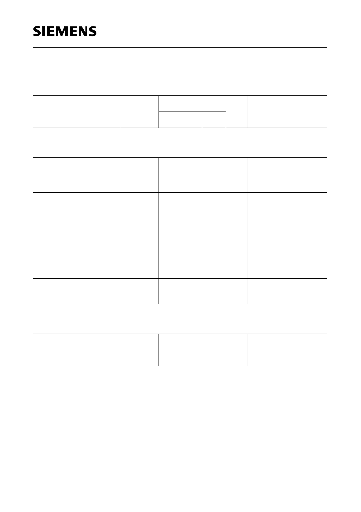
TLE 4214 G
Characteristics (cont’d)
V
= 6 to 16 V (typ. VS = 12 V); Tj = – 40 to 150 °C (typ. Tj = 25 °C)
S
Parameter Symbol Limit Values Unit Test Condition
min. typ. max.
Logic
Control inputs
H-input voltage threshold
L-input voltage threshold
V
V
IH
IL
1.3
0.9
1.8
1.2
2.1
1.5
V
V
–
–
Hysteresis of control
∆
V
I
input voltage
Enable input
H-input voltage threshold
L-input voltage threshold
Hysteresis of enable
V
V
∆
FH
FL
V
F
input voltage
H-input current
L-input current
I
IH
– I
IL
Status Output (open collector)
L-saturation voltage V
Status delay time
osat
t
dS
0.2 0.6 1.0 V –
1.6
1.4
2.1
1.8
2.7
2.3
V
V
–
–
0.1 0.3 0.7 V –
0
0
–
–
10
10
µA
µA
V
= 5 V
I
V
= 0.5 V
I
0.1 0.2 0.4 V IO = 5 mA
82032µs
1)
1)
Period from the beginning of the disturbance at one channel (exception: overvoltage) until the 50 % value of
the status switching edge is reached.
Semiconductor Group 303
Page 11
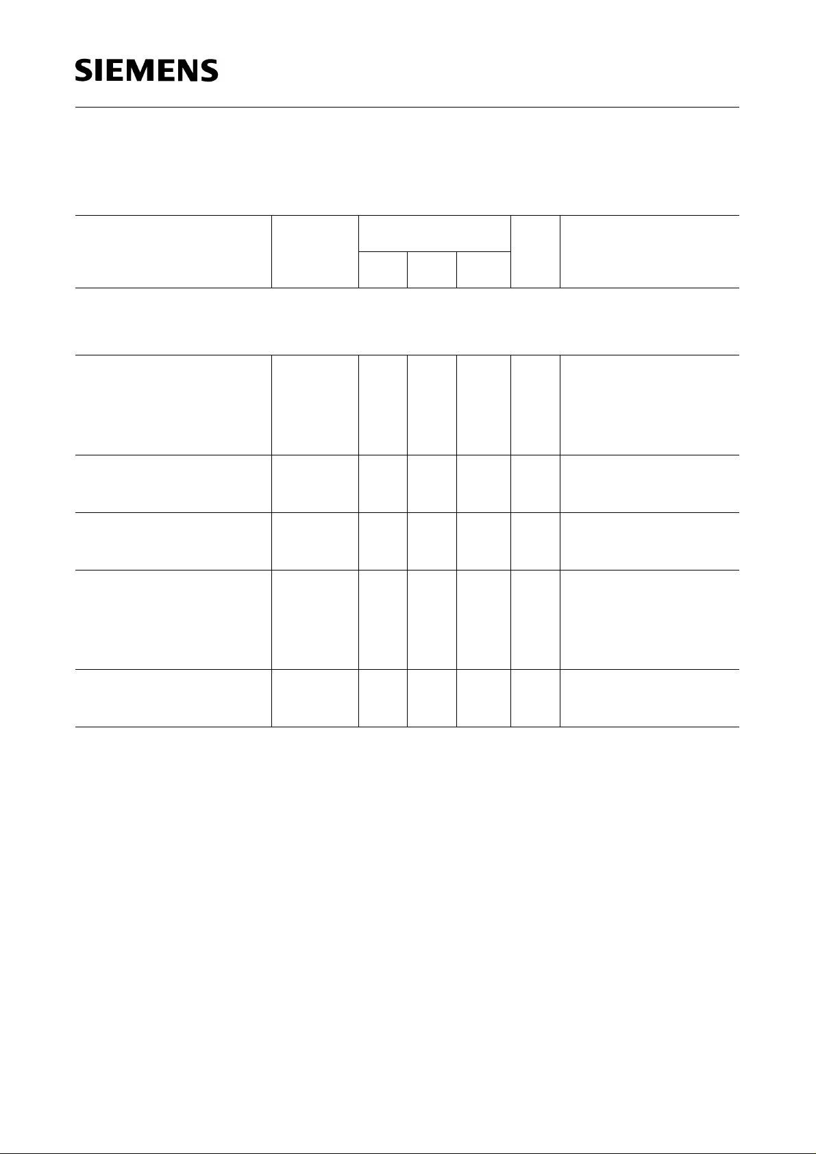
TLE 4214 G
Characteristics (cont’d)
V
= 6 to 16 V (typ. VS = 12 V); Tj = – 40 to 150 °C (typ. Tj = 25 °C)
S
Parameter Symbol Limit Values Unit Test Condition
min. typ. max.
Switching Stages
Saturation voltage
Saturation voltage
Output current
Leakage current
Switch-ON time
Switch-OFF time
Forward voltage of
substrate diode
Forward voltage of
clamp diode
Leakage current of
clamp diode
V
QSat
V
QSat
I
Q
I
Q
t
D ON
t
D OFF
V
QS
V
QF
–
I
QF
–
–
0.5
– 5––50
0.2
0.2
–
0.6450.8
100VmV
0.525
5
1.3
1.7
I
V
I
V
A
µA
µs
µs
V
V
V
I
I
I
= 0.5 A; VI > VIH;
Q
> V
F
= 50 mA; VI > VIH;
Q
> V
F
= 0.8 V; VI > V
QSat
= 6 V; VI < V
Q
= 0.5 Asee Timing
Q
= 0.5 ADiagram
Q
= – 0.5 A
Q
t < 0.1 s
–
1.3
1.7
V
I
= 0.5 A
Q
t < 0.1 s
––5 µAV
= 0 V; VI < V
Q
FH
FH
IH
IL
IL
Semiconductor Group 304
Page 12
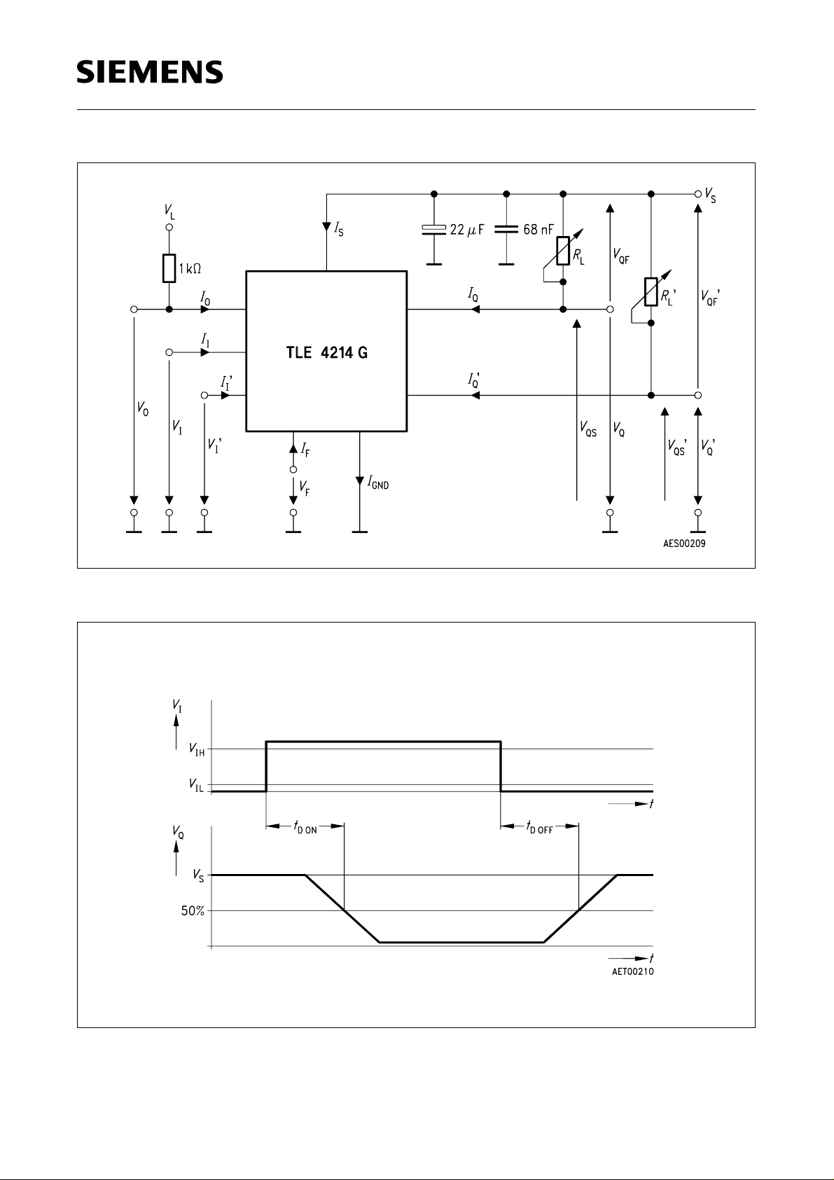
TLE 4214 G
Test Circuit
Timing Diagram
Semiconductor Group 305
Page 13
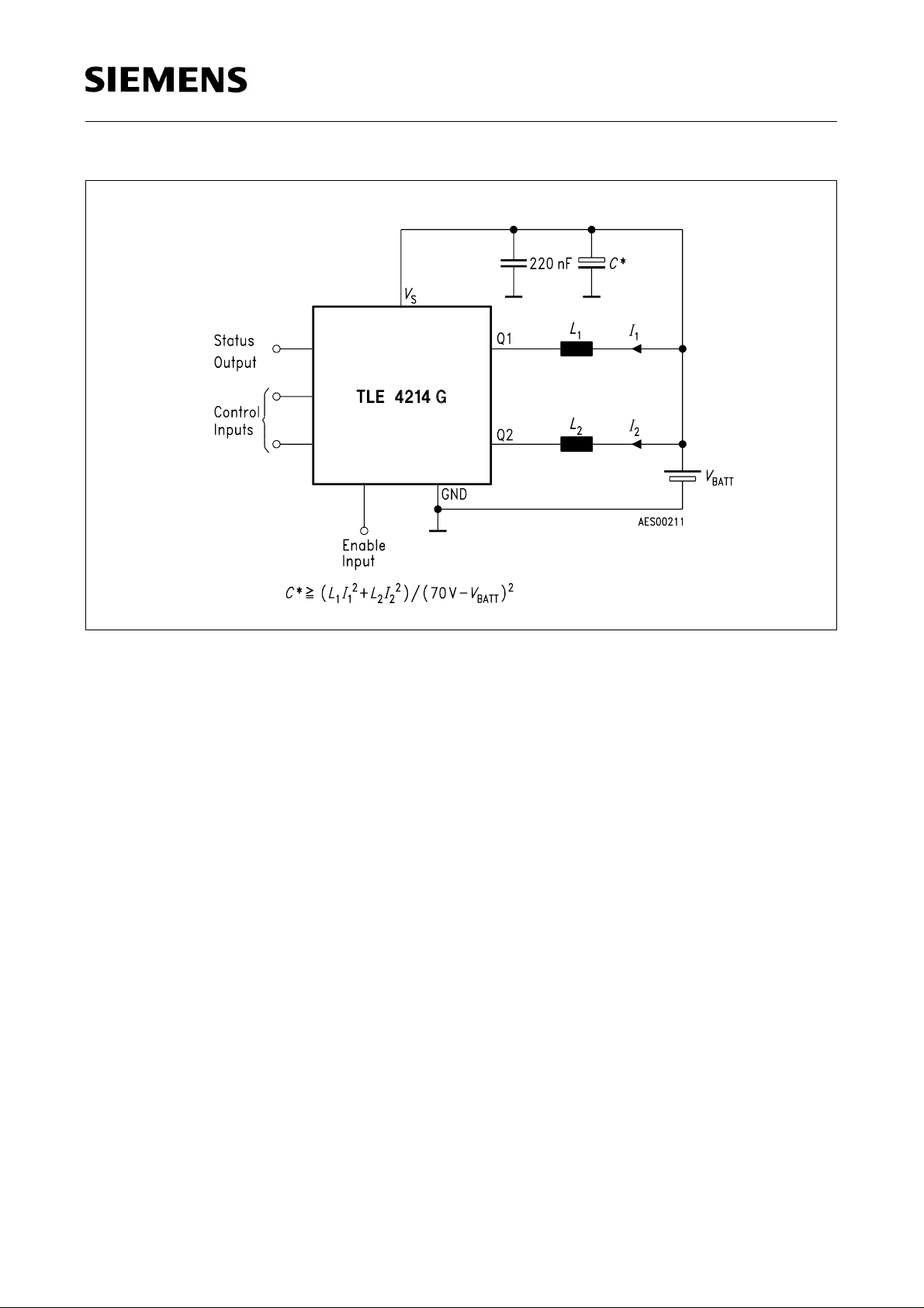
TLE 4214 G
Application Circuit
Semiconductor Group 306
Page 14
TLE 4214 G
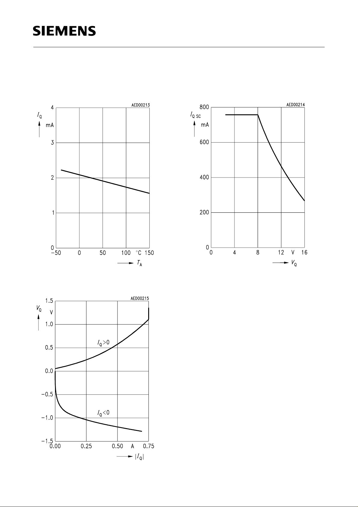
Quiescent Current IS versus Ambient
Temperature
V
= 12 V; VF < V
S
T
in the OFF-Status
A
FL
Shorted Load Current I
Q0
versus Output Voltage V
Q
Output Voltage VQversus
Output Current
V
= 12 V; VI > V
S
IH
Semiconductor Group 307
Page 15
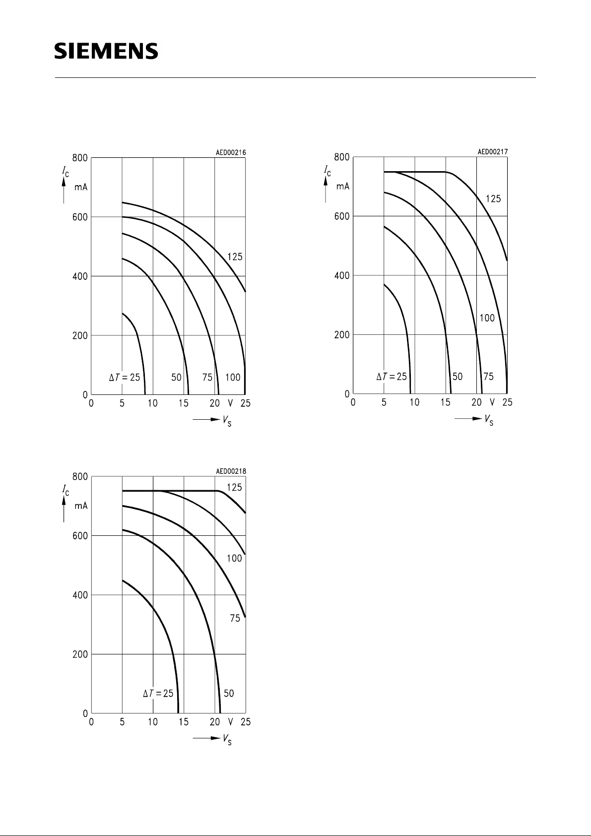
TLE 4214 G
Equal current at both channels
First channel 50 mA, second
channel
I
Q
Only one channel in operation
Semiconductor Group 308
Page 16
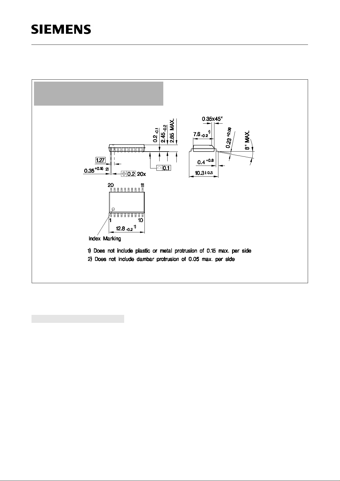
Package Outlines
P-DSO-20-7
(Plastic Dual Small Outline Package)
TLE 4214 G
Sorts of Packing
Package outlines for tubes, trays etc. are contained in our
Data Book “Package Information”.
SMD = Surface Mounted Device
GPSO5094
Dimensions in mm
Semiconductor Group 309
 Loading...