

Page 1
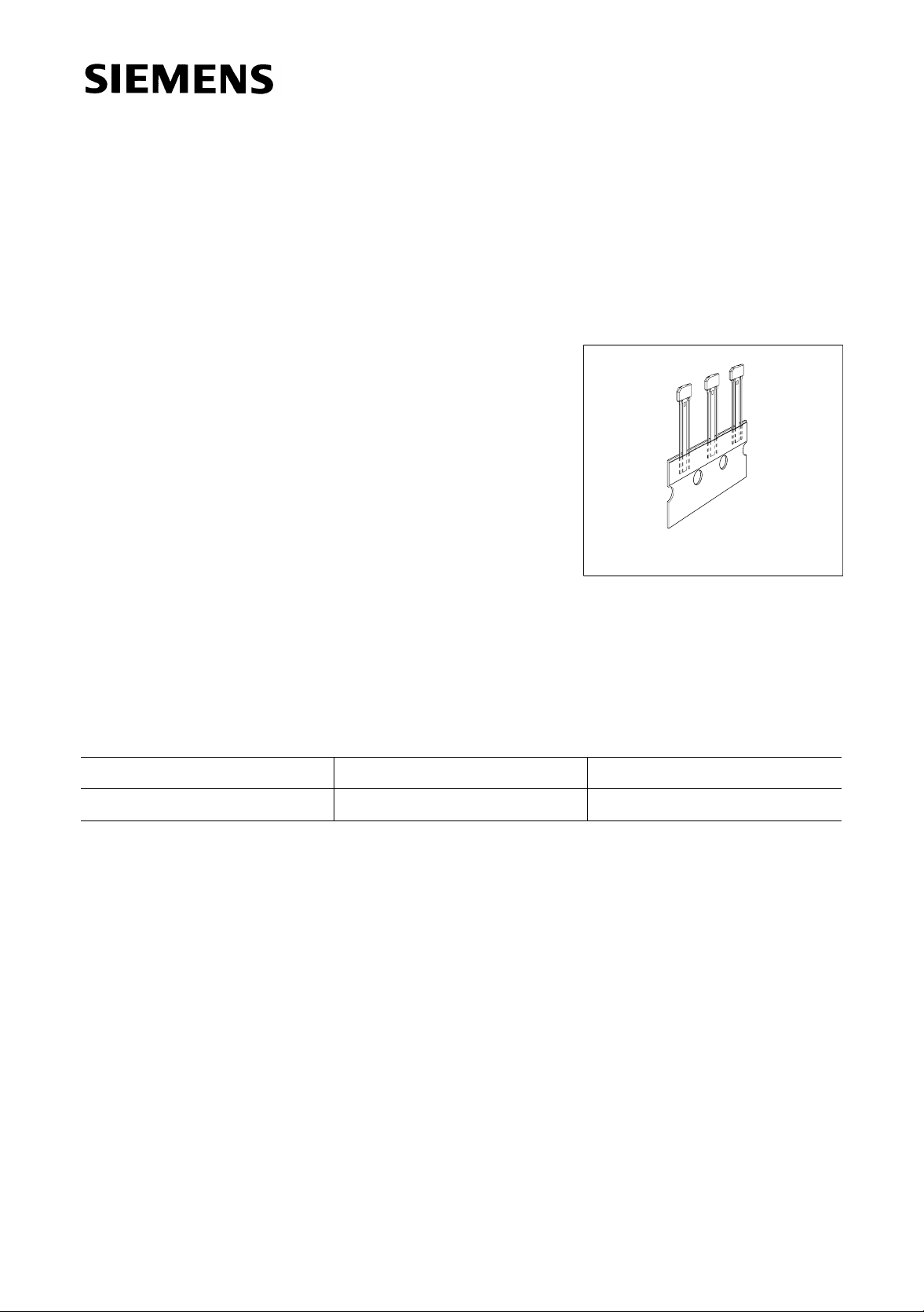
Dynamic Differential Hall Effect Sensor IC TLE 4923
Bipolar IC
Features
• Advanced performance
• Higher sensitivity
• Symmetrical thresholds
• High piezo resistivity
• Reduced power consumption
• South and north pole pre-induction possible
• AC coupled
• Digital output signal
• Two-wire interface
• Large temperature range
• Large airgap
• Low cut-off frequency
• Protection against reversed polarity
P-SSO-3-6
Type Ordering Code Package
▼ TLE 4923 Q62705-K408 P-SSO-3-6
▼ New type
The differential Hall effec t sensor TLE 4923 is compatible to the TLE 4921-3U, except
for having a 2-wire interface. The TLE 4923 provides high sensitivity, a superior stability
over temperature and symme trical thresholds in order to achieve a s table duty cycle.
TLE 4923 is particularly suitable for rotational speed detection and timing applications of
ferromagnetic toothed wheels such as in anti-lock braking systems, transmissions,
crankshafts, etc. The integrate d circuit (based on Hall effect) provides a dig ital signal
output with frequency proportional to the speed of rotation. Unlike other rotational
sensors differential Hall ICs are not influenced by radial vibration within the effective
airgap of the sensor and require no external signal processing.
Semiconductor Group 1 1998-04-29
Page 2
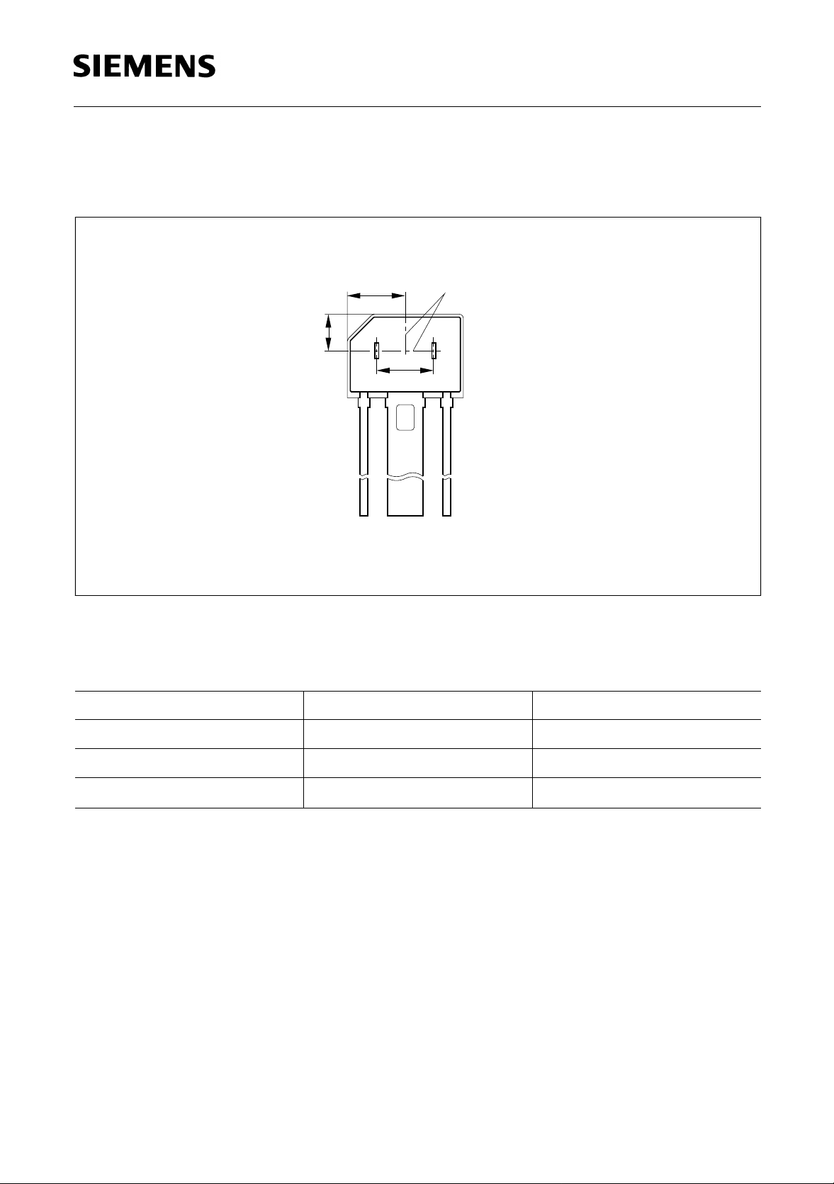
Pin Configuration
(top view)
1.53
2.67
TLE 4923
Center of
sensitive area ± 0.15
2.5
231
V
GND
S
C
AEP02039
Figure 1
Pin Definitions and Functions
Pin No. Symbol Function
1
V
S
Supply voltage
2 GND Ground
3
C
Capacitor
Semiconductor Group 2 1998-04-29
Page 3
TLE 4923
Protection
Device
1
V
S
Hall-Probes
Figure 2 Block Diagram
2
GND
Internal Reference and Supply
V
(3V)
reg
Highpass-
Amplifier
Filter
C
F
Schmitt-
Trigger
3
AEB01896
Semiconductor Group 3 1998-04-29
Page 4

TLE 4923
Functional Description
The Differential Hall sensor IC detects the motion and position of ferromagnetic and
permanent magnet structure s by mea suring the dif feren tial flux density of the mag netic
field. To detect ferromagne tic objects the magnetic field must be provided by a back
biasing permanent magnet (south or north pole of the magnet attached to the rear
unmarked side of the IC package).
Using an external cap acitor the gene rated Hall vo ltage signal is slowly adju sted via an
active high pass filter with low frequency cut-off. This causes the output to switch in to a
biased mode after a time constant is e lapsed. The time constant is determi ned by the
external capacitor. Filtering avoids aging and temperature influence from Schmitt-trigger
input and eliminates device and magnetic offset.
The TLE 4923 can be exploited to detect toothed wheel rotation in a rough environment.
Jolts against the toothed wheel and ripple have no influence on the output signal.
The on and off state of the IC are indicated by high and low current consumption.
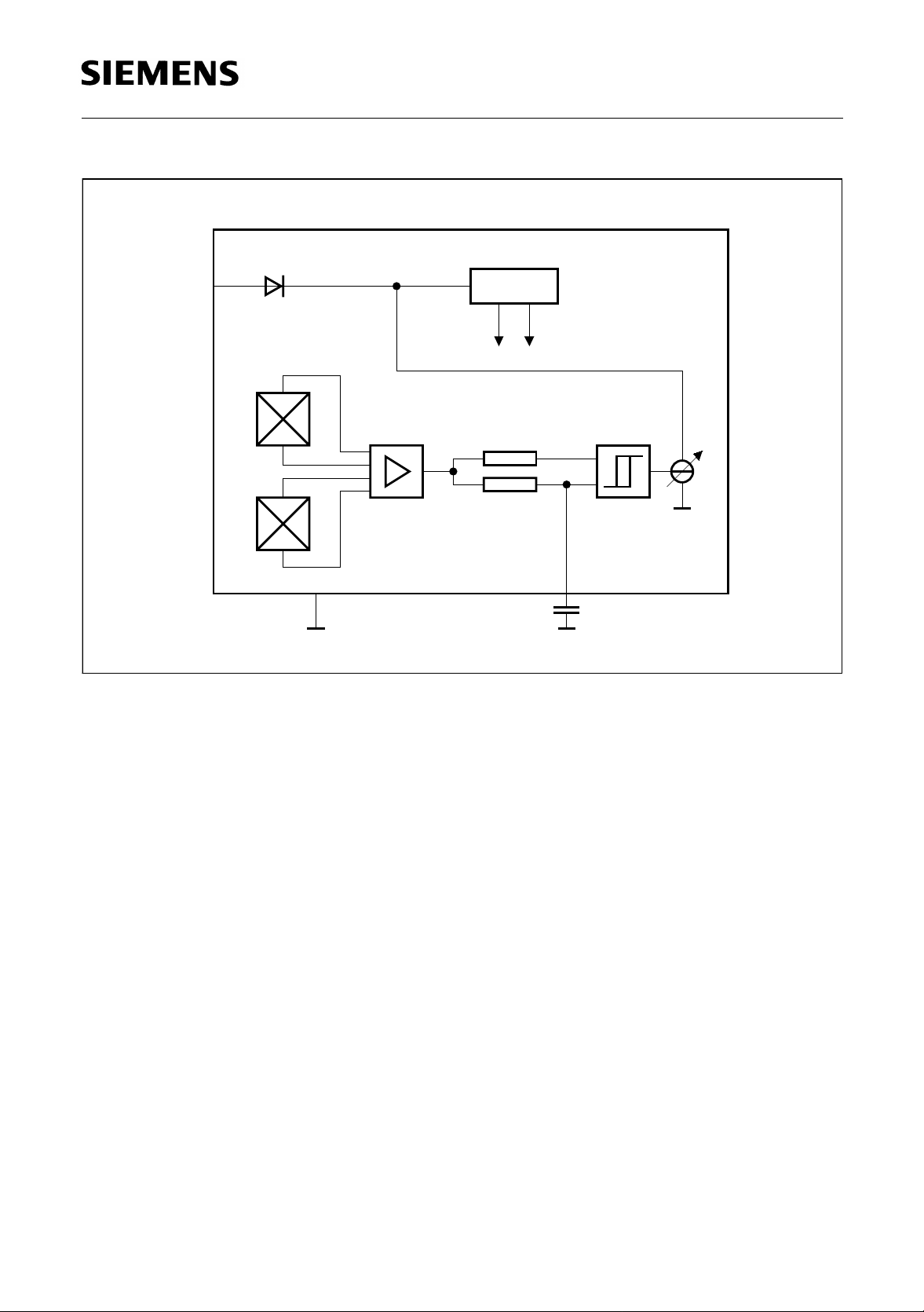
Circuit Description (see Figure 2)
The TLE 4923 is comprised of a supply voltage referenc e, a pair of Hall probes sp ace d
at 2.5 mm, differential amplifier, filter for offset compensation, Schmitt-trigger, and a
switched current source.
The TLE 4923 was designed to have a wide range of application parameter
variations. Differential fields up to ± 40 mT can be detected without influence to
the switching performance. The pre-induction field can either come from a
magnetic south or north pole, whereby the field strength up to 500 mT or more will
1)
not influence the switching points
. The improved temperature compensation
enables a superior sensitivity and accuracy over the tempera ture range. Finally,
the optimized piezo compensation and the integrated dynamic offset
compensation enable easy manufacturing and elimination of magnet offsets.
Protection is provided at the input/supply (pin 1) for reverse polarity.
1)
Differential bias fields exceeding ± 20 mT, e. g. caused by a mis aligned magnet, should be avoided.
Semiconductor Group 4 1998-04-29
Page 5
TLE 4923
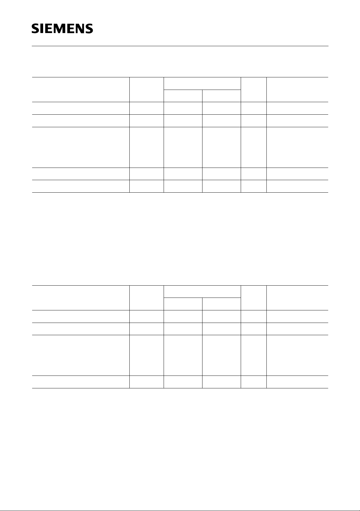
Absolute Maximum Ratings
Parameter Symbol Limit Values Unit Remarks
min. max.
Supply voltage
V
S
– 18
1)
24 V
Capacitor voltage
Junction temperature
Junction temperature
Junction temperature
Junction temperature
Storage temperature
Thermal resistance
1)
Reverse current drawn by the d ev ic e < 10 mA
2)
Can be reduced significant ly by f urt her packaging process, e. g. overm olding.
The device is ESD protected up t o 2 kV (HL test proc edure)
V
T
T
T
T
T
R
C
j
j
j
j
S
th JA
– 0.3 3 V
150
160
170
190
°C
°C
°C
°C
– 40 150 °C
190 K/W
5000 h
2500 h
500 h
4h
2)
Note: Stresses above those li sted here may cause permanent damage to the device.
Exposure to absolute maximum rating conditions for extended periods may affect
device reliability.
Operating Range
Parameter Symbol Limit Values Unit Remarks
min. max.
Supply voltage
Junction temperature
Pre-induction
V
T
B
S
j
0
4.5 18 V
– 40 190 °C
– 500 500 mT At Hall probe;
independent of
magnet
orientation
Differential induction ∆
B – 40 40 mT
Note: Unless otherwise noted, all temperatures refer to junction temperature.
In the operating range the functions given in the circuit description are fulfilled.
Semiconductor Group 5 1998-04-29
Page 6
TLE 4923
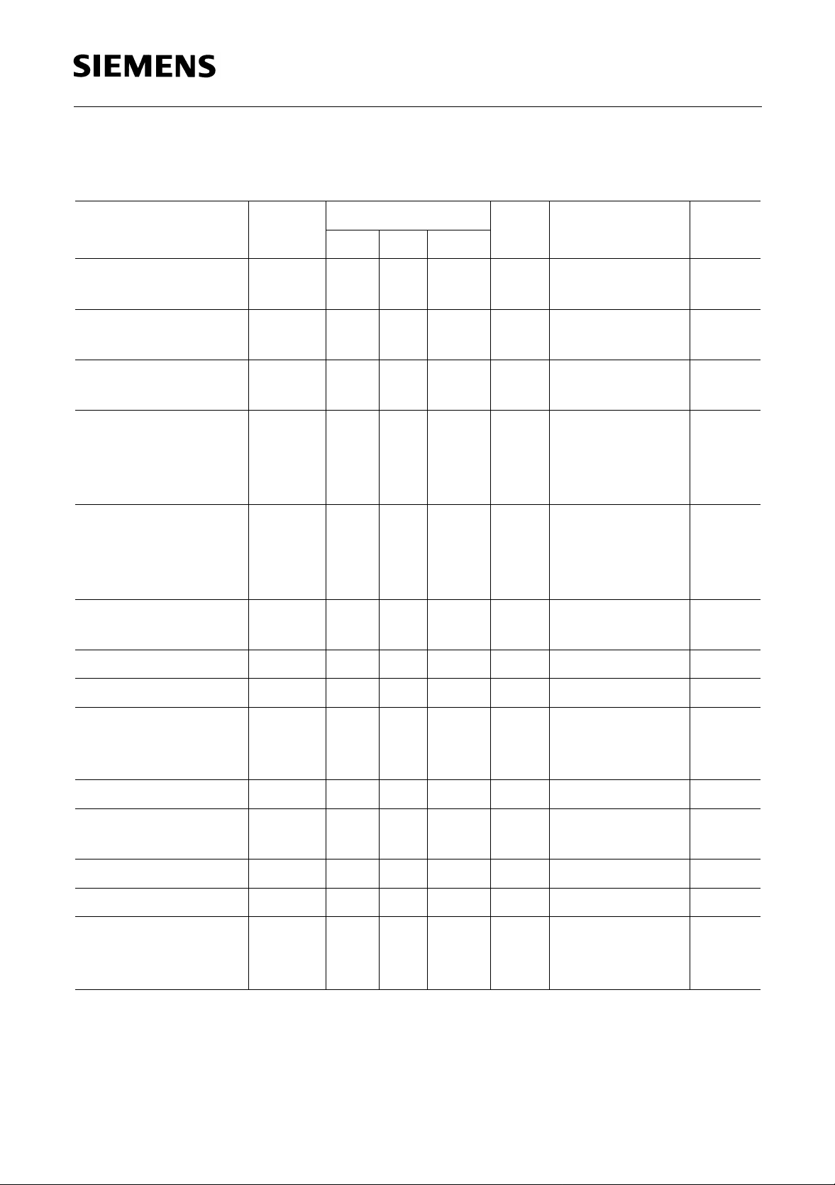
AC/DC Characteristics
The device characteristics listed below are guaranteed in the full operating range.
Parameter Symbol Limit Values Unit Test Condition Test
min. typ. max.
Circuit
Supply current
Supply current
difference
Supply current ratio
Center of switching
points:
B
(∆
+ ∆BRP) / 2
OP
Center of switching
points:
B
(∆
+ ∆BRP) / 2
OP
Hysteresis ∆
Current rise time
I
S
I
son
I
SON
I
SOFF
∆
B
∆
B
B
t
r
m
m
hy
- I
3.1
8.1
5.0 6.4 8.3 mA 1
soff
/
22.43 1
4.1
10.5
5.3
13.6
mA
mA
– 0.5 0 0.5 mT ∆B = 2.0 mT,
f = 200 Hz,
T
1) 2)
≤
j
– 40 °C<
150 °C
– 0.7 0 0.7 mT ∆B = 2.0 mT,
f = 200 Hz,
T
1) 2)
<
j
3)
150 °C<
190 °C
11.52.2mT∆B = 2.0 mT,
f = 200 Hz
0.5 µs2
1
1
2
2
2
Current fall time
Delay time
4)
Filter input resistance
Filter sensitivity to ∆
BS
Filter bias voltage
Frequency
Resistivity against
mechanical stress
(piezo)
6)
t
f
t
dop
t
drp
t
dop
R
C
V
f
∆B
∆B
0.5 µs2
25
10
- t
drp
C
35 43 52 kΩ 25 °C ± 2 °C1
15
µs
µs
µs
f = 10 kHz,
B = 5 mT
∆
2
8.5 mV/mT25 °C ± 2 °C1
C
m
Hy
1.6 2.0 2.4 V ∆B = 0 1
5)
– 0.1
– 0.1
10000 Hz ∆B = 5 mT 2
0.1
0.1
mT
mT
F = 2 N 2
Semiconductor Group 6 1998-04-29
Page 7
TLE 4923
∆B
m
ILR
C
T()×
S
C
T()
---------------------
=
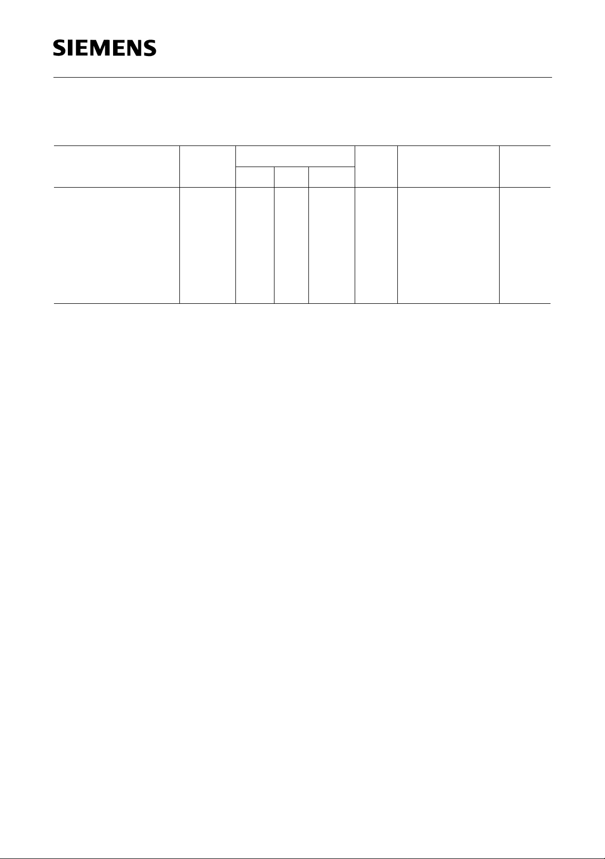
AC/DC Characteristics (cont’d)
The device characteristics listed below are guaranteed in the full operating range.
Parameter Symbol Limit Values Unit Test Condition Test
min. typ. max.
Power Supply
Rejection Ratio
(PSRR)
V
PSRR
10 V VS modulated
with
f
PSRR
t
r,fPSRR
B =0,
∆
V
,
PSRR
=10kHz,
=1µs,
only 1 transition
may occur
1)
For ∆B values larger than ± 10 mT this value may exceed the limits as follows: | ∆Bm | < | 0.05 × ∆B |
2)
Leakage currents at pin 3 sho uld be avoided. The bias shift of Bm caused by a leakage current IL can be
Circuit
7)
2
calculated by: . See also the typical curves on page 17.
3)
Differential pre-induction (e.g. by magnetic misalign m ent ) has t o be s m aller than 20 mT.
4)
For definition see Figure 6.
5)
Depends on filter capacit or CF. The cut-off frequency is given as . The switching points
are guaranteed over the whole frequency range, but amplitude modification and phase shift have to be taken
into account due to the 1
6)
For definition see Figure 7.
7)
For definition see Figure 5.
st
order highpass filter.
f
=
1
--------------------------------------- -
2 π×
R
× CF×
C
Note: The listed characteristic s are ensure d over the operating ra nge of the integ rated
circuit. Typical characte ristics speci fy mean val ues expected over the prod uction
Tj
spread. If not o therwise specified, t ypical characteristic s apply at
= 25°C and
the given supply voltage.
Semiconductor Group 7 1998-04-29
Page 8
TLE 4923
R
180
P
Ω
V
4.7 nF
∆
V
1)
R
C
=
C
Ι
∆
C
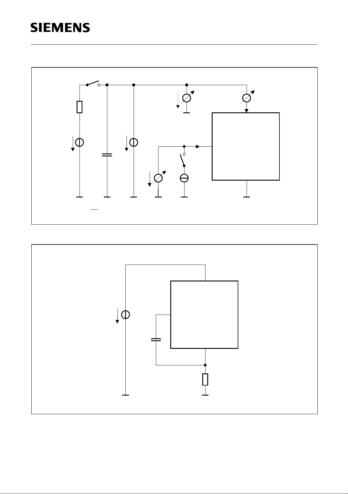
Figure 3 Test Circuit 1
V
SZ
Ι
S
1
V
S
1)
V
SLD
V
C
Ι
C
3
C
Ι
C
GND
2
AES01897
V
S
Figure 4 Test Circuit 2
1
V
S
3
C
C
F
1
µ
F
GND
2
AES01898
R
S
180
Ω
Semiconductor Group 8 1998-04-29
Page 9
18 V
PSRR
8 V
TLE 4923
t
r f
t
AED02488
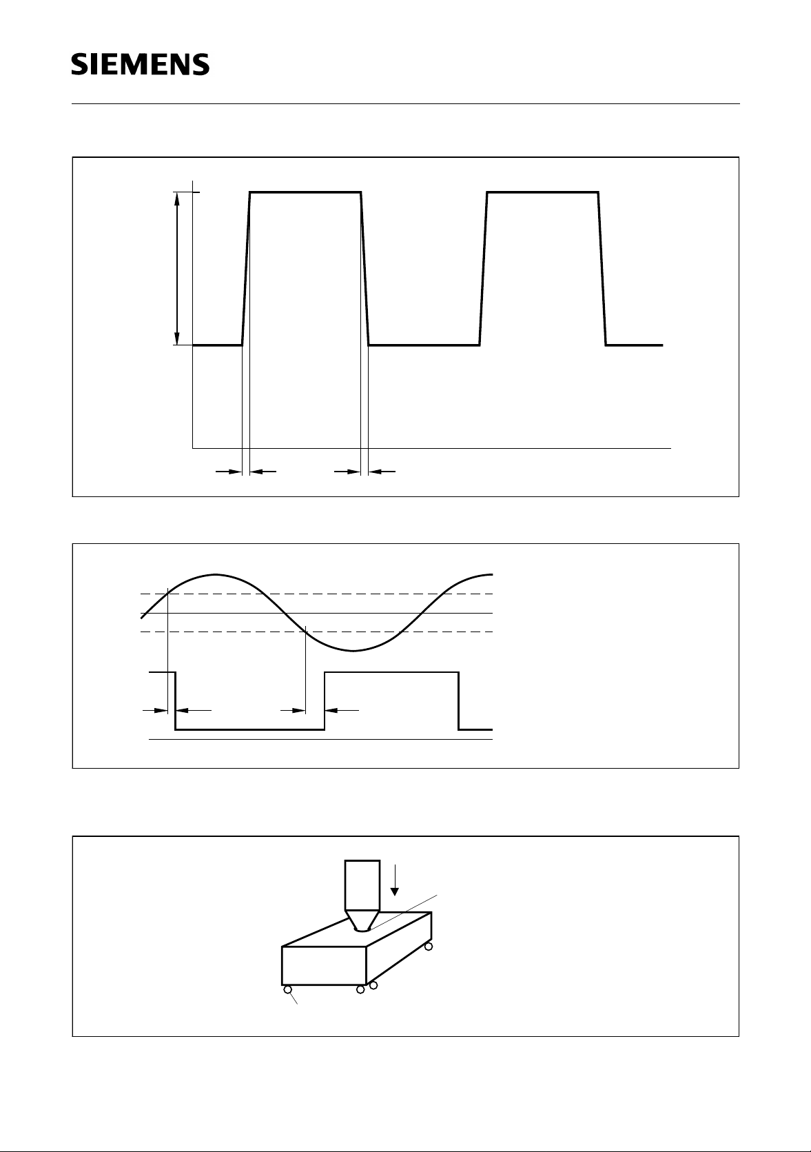
Figure 5
∆
B
∆
B
RP
∆
B
OP
t
drp
t
dop
Ι
t
Delay Time between:
drp
and
Ι
LOW to HIGH transient
S
t
Delay Time between
:
dop
S
Ι
and
HIGH to LOW transient
S
Figure 6 Definition of Delay Times (switching points related to initial
measurement @∆
B = 2 mT; f = 200 Hz)
B
∆ = ∆
∆
AED02509
B
RP
∆B=
B
OP
F = 2N
r = 0.5 ± 0.05 mm
IC
4 x d = 1.5
AEA02508
Figure 7 Setup for Piezo Measurements
Semiconductor Group 9 1998-04-29
Page 10
TLE 4923
Application Notes
Two possible applications are shown in Figure 10 and Figure 11 (Toothed and Magnet
Wheel).
Two-wire ap plication i s shown in Figure 12.
Gear Tooth Sensing
In the case of ferrom agnetic too thed wheel a pplicat ions the IC has to be biase d by the
south or north pole of a permanent magnet (e.g. SmCo
the dimensions 8 mm × 5mm× 3 mm) which should cover both Hall probes.
The maximum air gap depends on:
– the magnetic field strength (magnet used; pre-induction) and
– the tooth wheel that is used (dimensions, material, etc.; resulting differential field).
(Vacuumschmelze VX170) with
5
a centered distance
of Hall probes
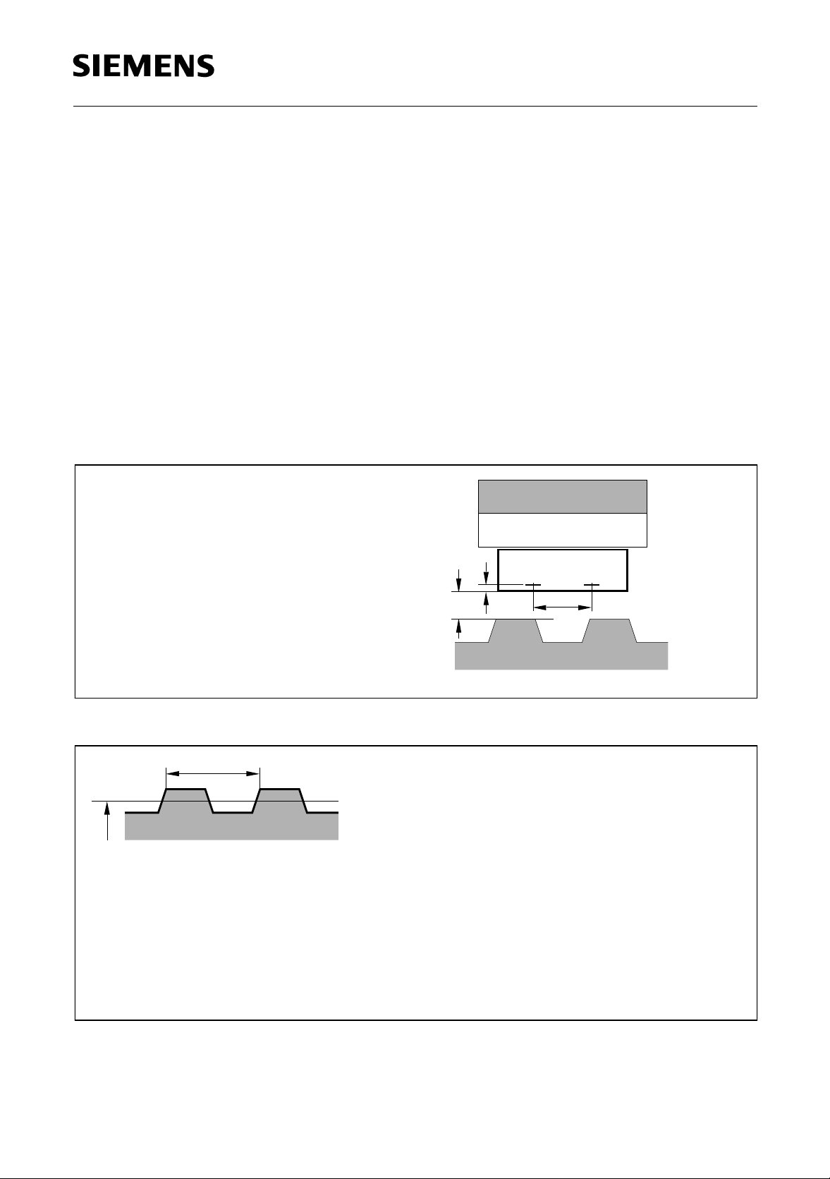
b Hall probes to
IC surface
L IC surface to
tooth wheel
a=2.5mm
b = 0.3 mm
Figure 8 Sensor Spacing
T
d
AEA01260
DIN
d diameter (mm)
z number of teeth
m module m = d/z (mm)
T pitch T = π × m (mm)
N
S
b
L
a
AEA01259
Conversion DIN – ASA
m = 25.4 mm/p
T = 25.4 mm CP
ASA
p diameter pitch p = z/d (inch)
PD pitch diameter PD =
z/p (inch)
CP circular pitch CP = 1 inch × π/
p
Figure 9 Tooth Wheel Dimensions
Semiconductor Group 10 1998-04-29
Page 11
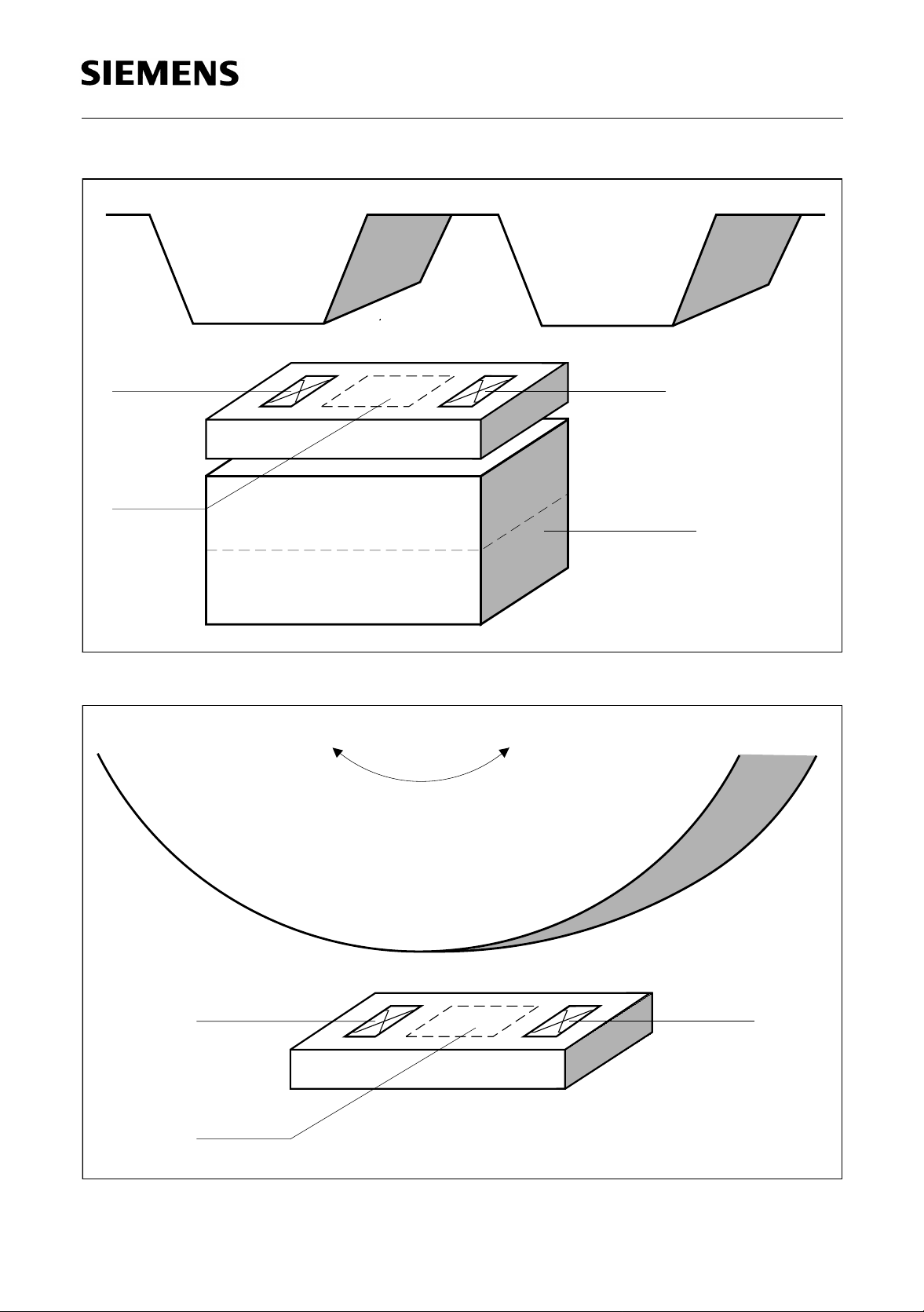
Gear Wheel
TLE 4923
Hall Sensor 1
Signal
Processing
Circuitry
(N)S
Hall Sensor 2
Permanent Magnet
(S)N
AEA01261
Figure 10 TLE 4923, with Ferromagnetic Toothed Wheel
Magnet Wheel
S
S
N
Hall Sensor 1
Signal
Processing
Circuitry
AEA01262
Figure 11 TLE 4923, with Magnet Wheel
Semiconductor Group 11 1998-04-29
Hall Sensor 2
Page 12
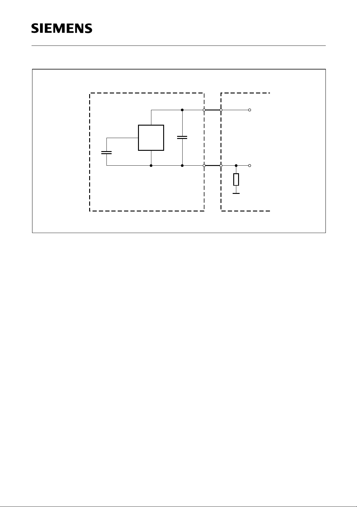
Two-wire-application
TLE 4923
3
C
F
1
µ
F
Ω
180=
R
typical :
S
Figure 12 Application Circuit
Line
1
V
S
C
1
C
4.7 nF
S
V
S
GND
2
V
SIGNAL
R
S
Sensor Mainframe
AES01899
Semiconductor Group 12 1998-04-29
Page 13
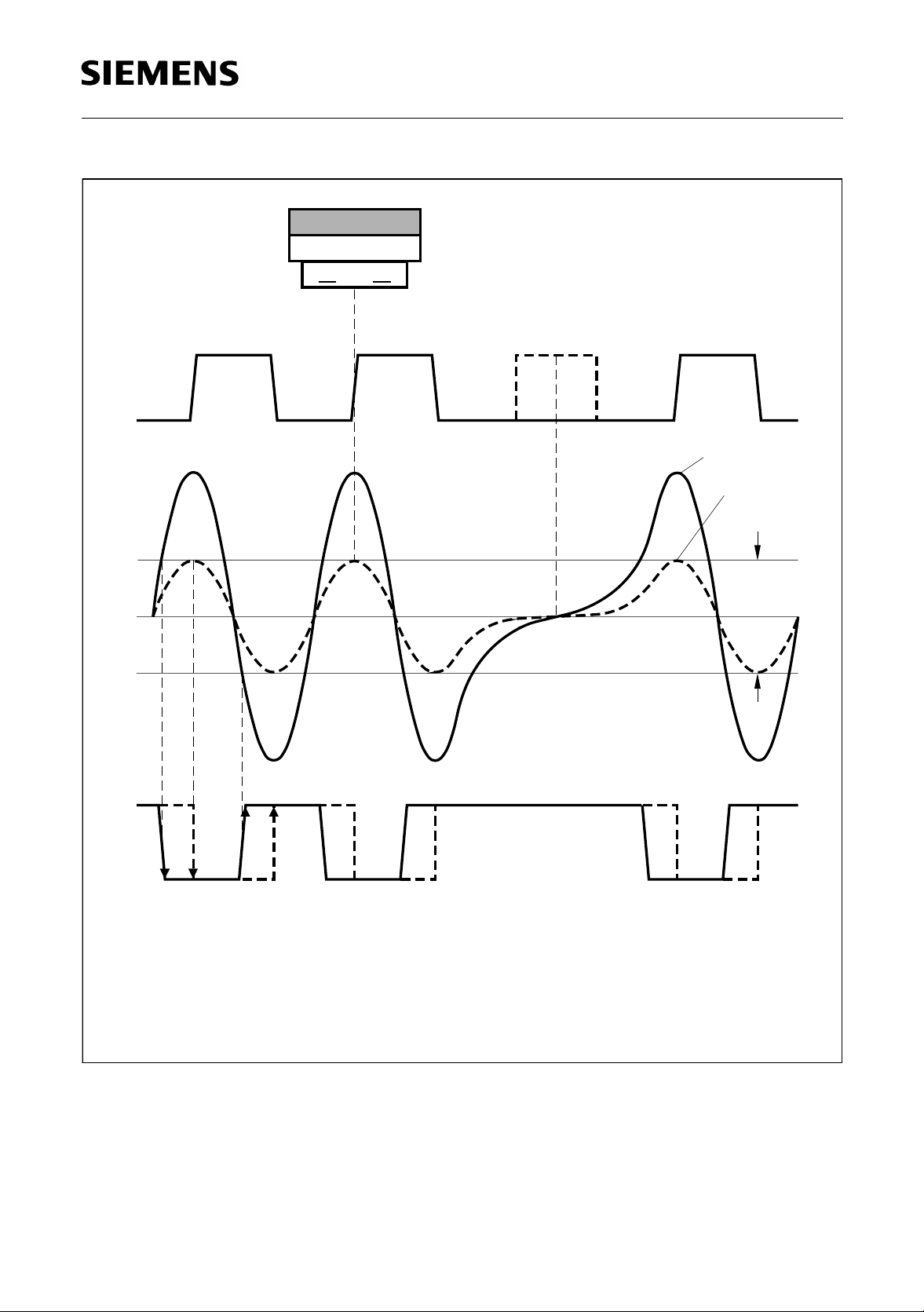
TLE 4923
N(S)
S(N)
13
B1 B2
Missing ToothWheel Profile
Magnetic Field Difference
B = B2-B1
∆
B
∆
RP
= 0.75 mT
Output Signal
Ι
S
Small Airgap
Large Airgap
B
∆
HY
B
= -0.75 mT∆
OP
Operate point : B2-B1<
Release point : B2-B1>
∆∆∆
B
RP
switches the output ON
∆
B
OP
∆
B
switches the output OFF
RP
=
+
B
B
HYOP
(
high
low
current
(
The magnetic field is defined as positive if the south pole of
the magnet shows towards the rear side of the IC housing.
AED01900
Figure 13 System Operation
Semiconductor Group 13 1998-04-29
Page 14
TLE 4923
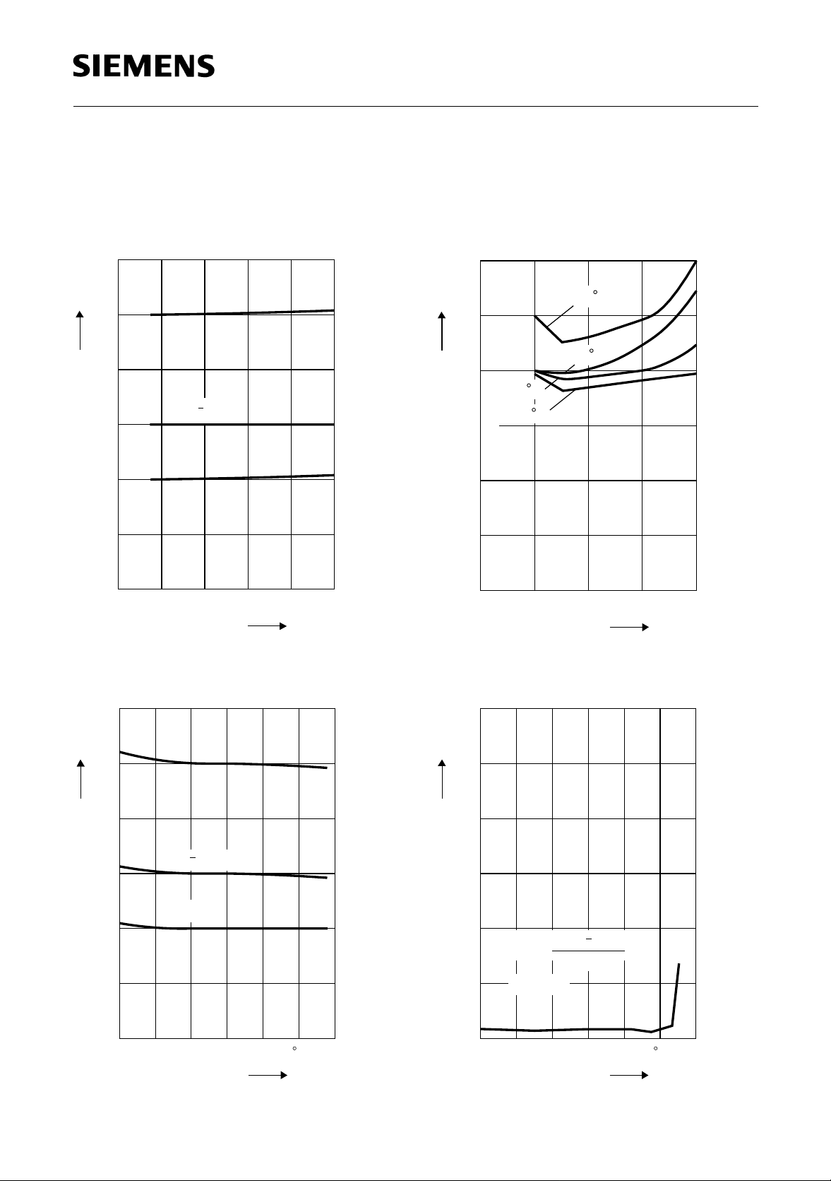
If not otherwise specified, all curves reflect typical values at Tj = 25 °C and
V
=12V.
S
Supply Current and Supply Current
Difference versus Supply Voltage
12
mA
Ι
S
Ι
SON
10
8
Ι
Ι
SON
SOFF
6
Ι
SOFF
4
AED02473
Minimum Switching Field versus
Frequency
1.2
mT
T
B
min
= 190 C
j
1.0
T
= 150 C
j
0.8
T
= 25 C
j
T
= -40 C
j
0.6
0.4
AED02475
2
0
0
5
10
15 25
20
V
V
S
Supply Current and Supply Current
Difference versus Temperature
12
mA
Ι
S
Ι
SON
10
8
ΙΙ
SON
SOFF
6
Ι
SOFF
4
2
AED02474
0.2
0
1
10
100 10000
1000
Hz
f
Mean Value of Switching Induction
1.2
mT
∆
B
m
1.0
0.8
0.6
0.4
0.2
∆
∆
B
=
m
f
= 200 Hz
∆
B
B
OP
2
AED02476
RP
typ
0
400-40
80 200
120
C
T
j
0
400-40
80 200
120
C
T
j
Semiconductor Group 14 1998-04-29
Page 15
TLE 4923
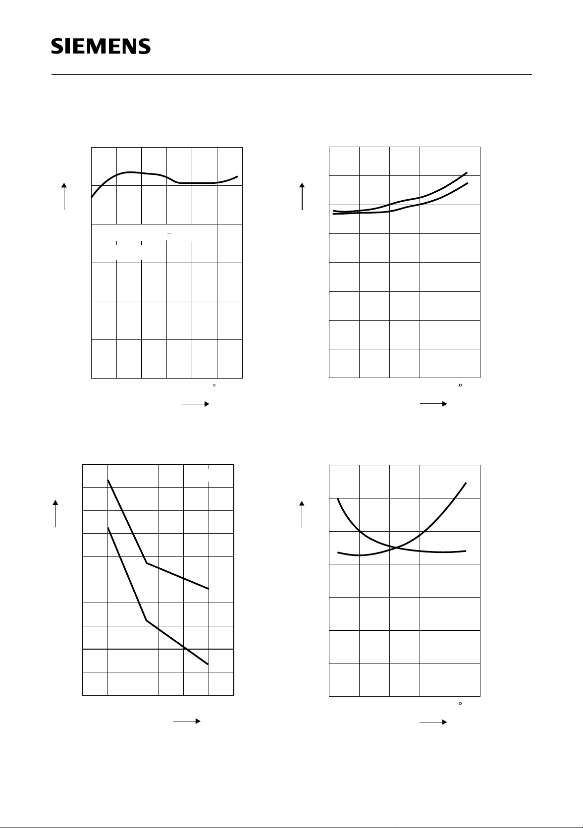
Hysteresis versus Temperature
1.6
mT
∆
B
HY
1.4
1.2
∆
∆
HY
B
=
RP
∆
B
f
= 200 Hz
1.0
0.8
0.6
0.4
400-40
80 200
B
120
OP
AED02477
typ
C
T
j
Delay Time1) versus Temperature
8
µ
s
t
d
7
6
5
4
3
2
1
0
500-50
100
AED02479
t
dop
t
drp
150
C
T
j
200
Delay Time1) versus Differential Field
6.0
s
µ
5.9
t
d
5.8
5.7
5.6
5.5
5.4
5.3
5.2
5.1
5.0
0
6
42
AED02478
= 10 kHz
f
8
mT
∆
t
dop
t
drp
12
B
Rise and Fall Time versus Temperature
AED02480
150
C
T
j
200
t
140
ns
120
100
80
60
40
20
t
f
t
r
0
500-50
100
1)
Switching points related to init ial m easurement
B = 2 mT, f = 200 Hz
@∆
Semiconductor Group 15 1998-04-29
Page 16
TLE 4923
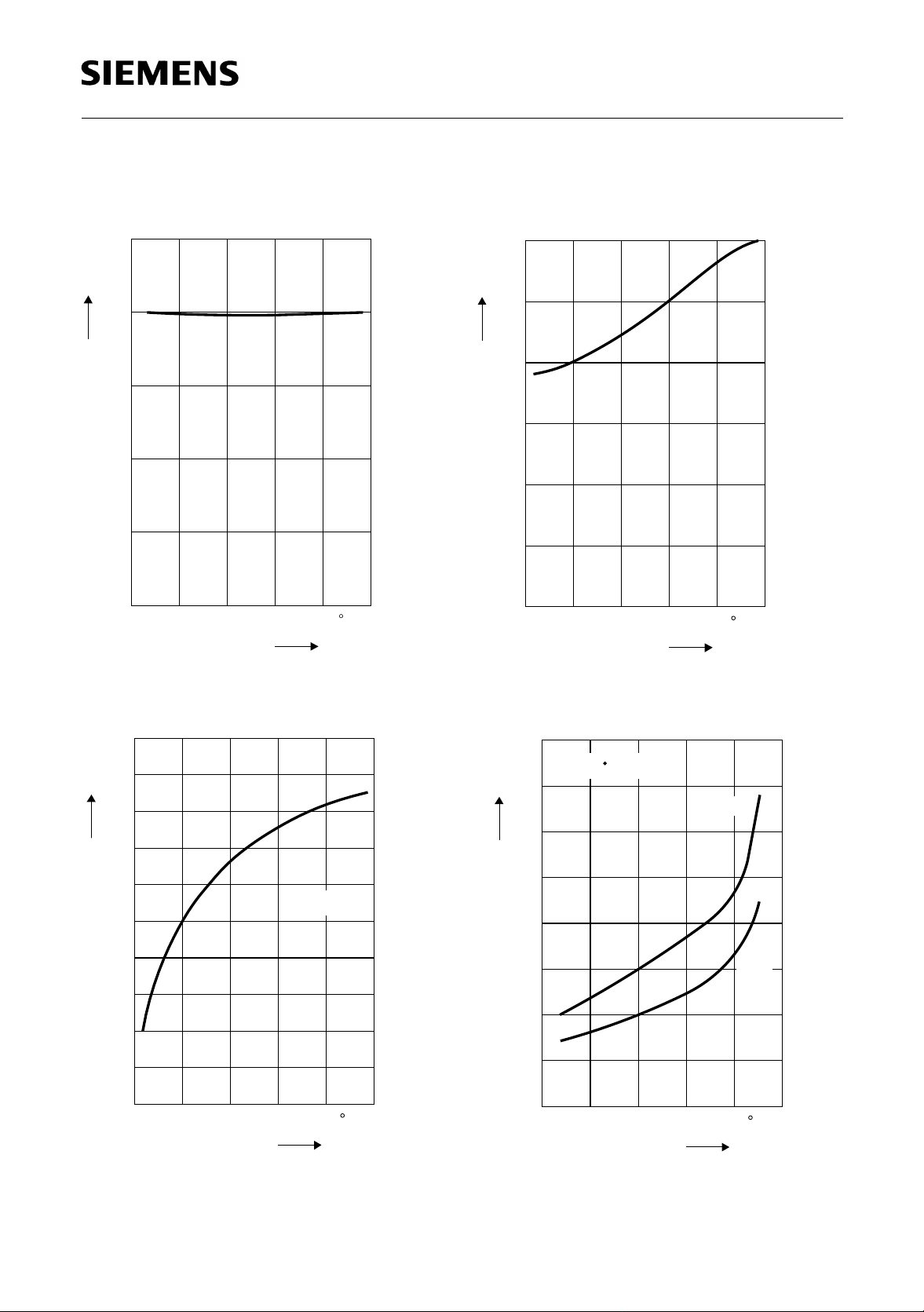
Capacitor Voltage versus Temperature
2.5
V
V
C
2.0
typ
1.5
1.0
0.5
0
500-50
100 200
AED02481
150
C
T
j
Filter Input Resistance versus
Temperature
60
k
Ω
R
C
50
typ
40
30
20
10
0
500-50
100 150
AED02483
C
T
j
200
Filter Sensitivity versus Temperature
0
mV/mT
-2
S
C
-4
-6
-8
-10
-12
-14
-16
-18
-20
500-50
typ
100 150
AED02482
= 12 V
V
S
T
j
200
C
t
Delay Time
for Power ON versus
pon
Temperature
0.8
ms/nF
k
0.7
t
= k (nF)
pon
C
F
0.6
0.5
0.4
0.3
0.2
0.1
0
500-50
100
1)
Calculated values for minimum and maximum filter
resistance, at room temperature.
C
F
AED02484
1)
max.
min.
150
T
j
1)
200
C
Semiconductor Group 16 1998-04-29
Page 17
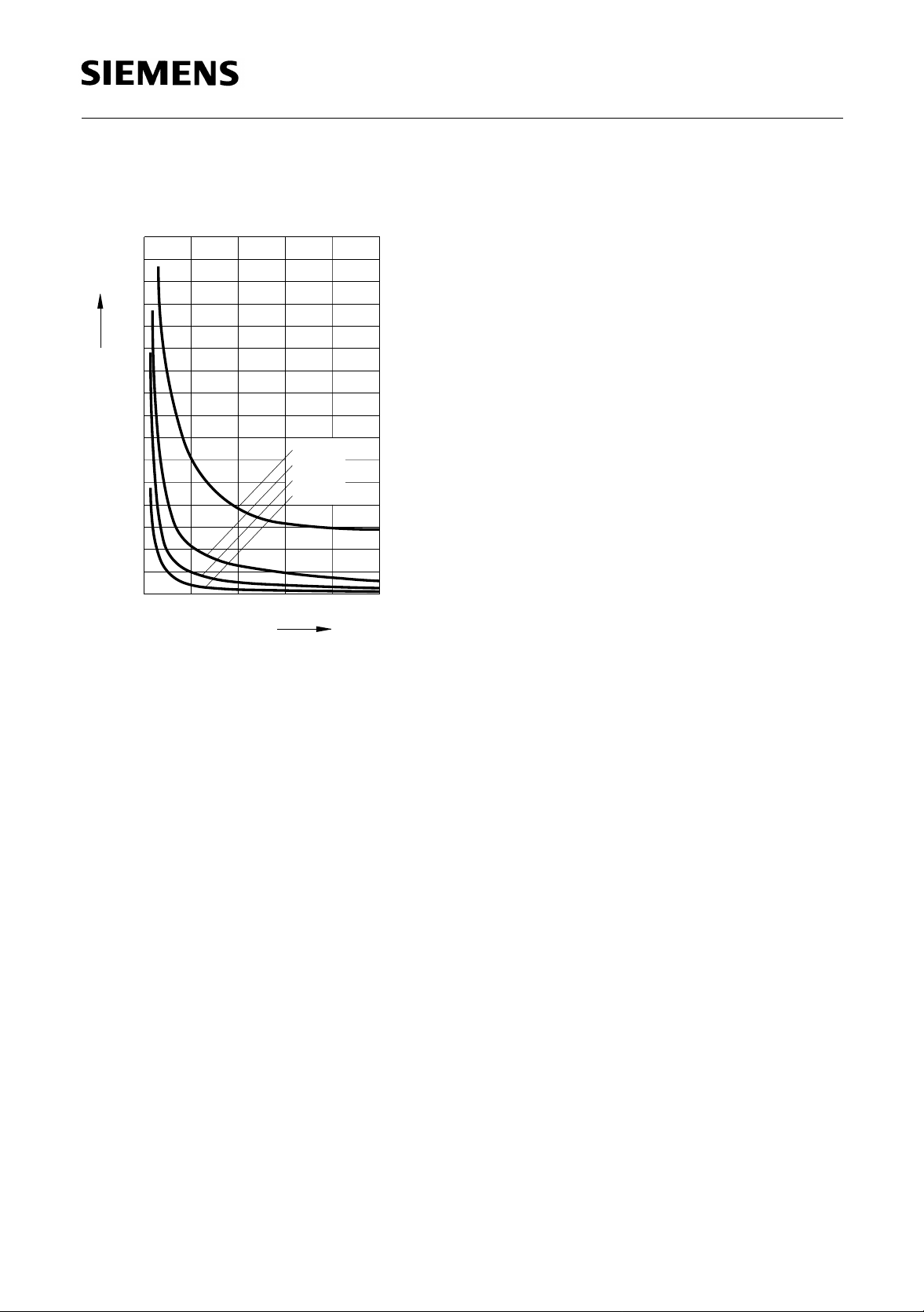
Threshold Shift versus Filter Leakage
8
mT
∆
B
7
m
6
5
4
AED02485
TLE 4923
3
2
1
0
0
20
40 60 80 100M
+190˚C
+100˚C
+25˚C
-40˚C
Ω
R
C
Semiconductor Group 17 1998-04-29
Page 18
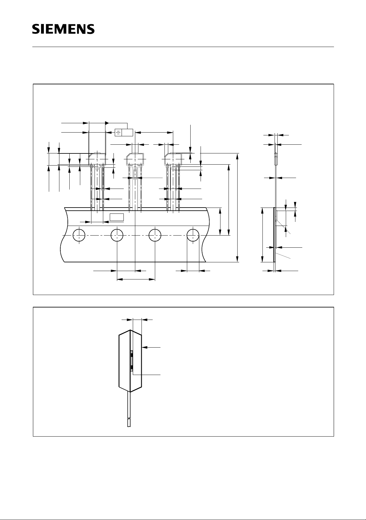
Package Outline
P-SSO-3-6
(Plastic Single Small Outline Package)
±0.08
5.16
±0.05
5.38
0.2
max.1.9 1 x 45˚
12.7
±1
0.15 max.
±0.1
1.2
1
-0.1
TLE 4923
±0.05
0.25
±0.08
3.71
±0.06
3.38
±0.1
0.65
(0.25)
1 max.
0.87
±0.05
0.6 max.
±0.05
0.4
123
3.81
±0.4 ±0.3
6.35
±0.3
12.7
d
Branded Side
1.9 max.
±0.05
1.67
4
+0.759-0.5
±0.5
23.8
max.38
±0.5
18
+0.1
0.2
-1
1
±0.5
6
Adhesive Tape
0.25
-0.15
Tape
±0.1
0.5
GPO05960
Hall-Probe
d : Distance chip to upper side of IC
P-SSO-3-6 : 0.3
±0.08
mm
AEA02510
Sorts of Packing
Package outlines for tubes, trays etc. are contained in our
Data Book “Package Information”.
Dimensions in mm
Semiconductor Group 18 1998-04-29
 Loading...