

Page 1
Intelligent Sixfold Low-Side Switch
Features
● Quad 50 mA outputs
● Dual 500 mA outputs
● Operating range V
● Output stages with power limiting
● Open-collector outputs
● Shorted load protected within operating range
● Clamp-diodes to ground
● Status signaling
● TTL-compatible control inputs
● Overtemperature monitoring
● Temperature range – 40 to 125 ˚C
= 5 V ± 5 %
S
TLE 4226 G
Bipolar-IC
P-DSO-24-3
Type Ordering Code Package
▼
TLE 4226 G Q67000-A9118 P-DSO-24-3 (SMD)
▼ New type
TLE 4226 G is an integrated, sixfold low-side power switch with power limiting of the 0.5 A outputs,
shorted-load protection of the 50 mA switches and Z-diodes on all switches from output to ground.
TLE 4226 G is particularly suitable for automotive and industrial applications.
Semiconductor Group 1 07.96
Page 2
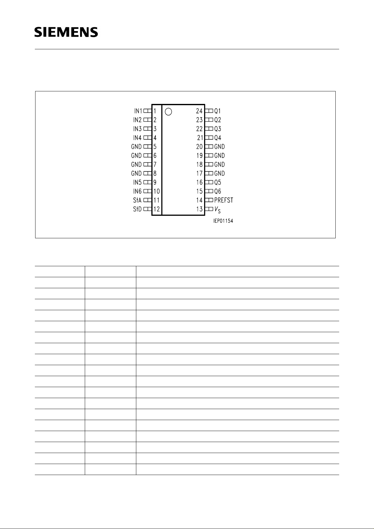
Pin Configuration
(top view)
TLE 4226 G
Pin Definitions and Functions
Pin Symbol Function
1 IN1 Input switch 1, active high (50 mA)
2 IN2 Input switch 2, active high (50 mA)
3 IN3 Input switch 3, active high (50 mA)
4 IN4 Input switch 4, active high (50 mA)
5, 6, 7, 8 GND Ground, cooling
9 IN5 Input switch 5, active high (500 mA)
10 IN6 Input switch 6, active high (500 mA)
11 StA Status output analog
12 StD Status output digital (error = low)
13
V
S
Supply voltage
14 PREFST Preferred state input, active low
15 Q6 Output switch 6 (500 mA)
16 Q5 Output switch 5 (500 mA)
17, 18, 19, 20 GND Ground, cooling
21 Q4 Output switch 4 (50 mA)
22 Q3 Output switch 3 (50 mA)
23 Q2 Output switch 2 (50 mA)
24 Q1 Output switch 1 (50 mA)
Semiconductor Group 2
Page 3
TLE 4226 G
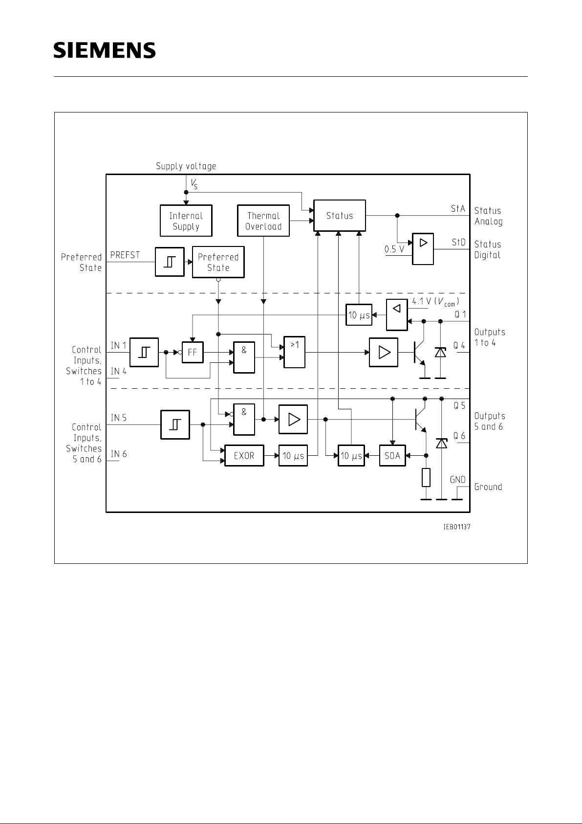
Block Diagram
Semiconductor Group 3
Page 4
TLE 4226 G
Application Description
Applications in automotive electronics call for intelligent power switches that can be activated by
logic signals, which have to be shorted load protected and which provide error feedback.
This IC contains six power switches connected to ground (low-side switches). On inductive loads
the integrated Z-diodes clamp the discharging voltage.
By means of TTL signals on the control inputs (active high) all six switches can be activated
independently of one another when a high level appears on the preferred-state input. When there
is a low level on the preferred-state input, switches 1 to 4 are switched on, switches 5 and 6 are
switched off regardless of the control-input levels. The inputs are highly resistive and therefore must
not be left unconnected but should always be on fixed potential (noise immunity). Inputs that are not
used, should be connected to low level to reduce the power consumption.
The analog status output signals the following errors by analog voltage levels:
– Overload
– Thermal overload
– Openload or shorted load to ground (only switches 5 and 6)
The following levels signal errors at the analog and digital status outputs.
Errors Analog Status Digital Status
Normal function Low High
Overload
Openload or shorted load to ground (only switches 5 and 6)
Thermal overload
1.0 V to 3.3 V
1.0 V to 1.7 V
> 3.5 V
Low
Low
Low
Possible Input and Output Levels
Supply Voltage
2 to 5 V
5 V
5 V
V
PREFST IN1-6 Q1-Q4 Q5, Q6
S
Low
High
High
Random
Low
High
Low
High
Low
High
High
Low
Semiconductor Group 4
Page 5

TLE 4226 G
Circuit Description
Input Circuits
The control inputs and the preferred-state input consist of TTL-compatible Schmitt triggers with
hysteresis. Driven by these stages the buffer amplifiers convert the logic signal necessary for driving
the NPN power transistors.
Switching Stages
The output stages consist of NPN power transistors with open collectors. Each stage has its own
protective circuit for limiting power dissipation and shorted load current, which makes the outputs
shorted load protected to the supply voltage throughout the operating range. Integrated clampdiodes limit positive voltage spikes that occur when inductive loads are discharged. Output currents,
caused through negative voltages at the outputs, are compensated up to 50 mA for all outputs in
total.
Monitoring and Protective Functions
Each output is monitored (for overload) in its activated status. For the switches 1 to 4 overload is
detected, if the switches are activated and the output voltage at the transistor is higher than 4.1 V
for more than 10 µs. The concerned output will be shutdown and both status outputs will be set. The
switch can only be activated again if the corresponding input is switched off and then on again. If
the output voltage does not exide 4.1 V, the output is not shutdown and the status outputs are not
set, although an overload may occur. The switches 5 and 6 are protected through a SOA-circuit. It
is suppressed for at least 10 µs when the switch is turned on before it can start limiting the overload
current. The status outputs also monitor openload or shorted load to ground at the switches 5 and
6 in deactivated mode.
An analog signal is applied to the analog status output only when protection function is active. If
several malfunctions appear coincident, the highest voltage level of the analog status output will
dominate. Simultaniously the digital status output will be set.
The IC is also protected against thermal overload. If a chip temperature of typically 155 ˚C is
attained, the status outputs monitor overtemperature. If the temperature continues to increase, the
inputs and outputs of the switches 5 and 6 are shutdown. The switches 1 to 4 will not shutdown, so
precaution has to be taken in the application to prevent a further increase of the chiptemperature,
which may destroy the IC. After cooling down below 140 ˚C the overtemperature monitoring will be
reseted and the outputs of the switches 5 and 6 can be activated again.
If the minimum supply voltage for operation is not maintained, the outputs are deactivated. At a
supply voltage of higher than 1.8 V, the outputs 1 to 4 are switched on, if pin 14 (PREFST) is
connected to ground over a resistance smaller 1 MΩ. The outputs 1 to 4 can be controlled via the
inputs, if pin 14 (PREFST) is switched to high or not connected. Characteristics may be beyond the
specified values. Full function is guaranteed in the supply voltage range of 5 V ± 5%.
Semiconductor Group 5
Page 6
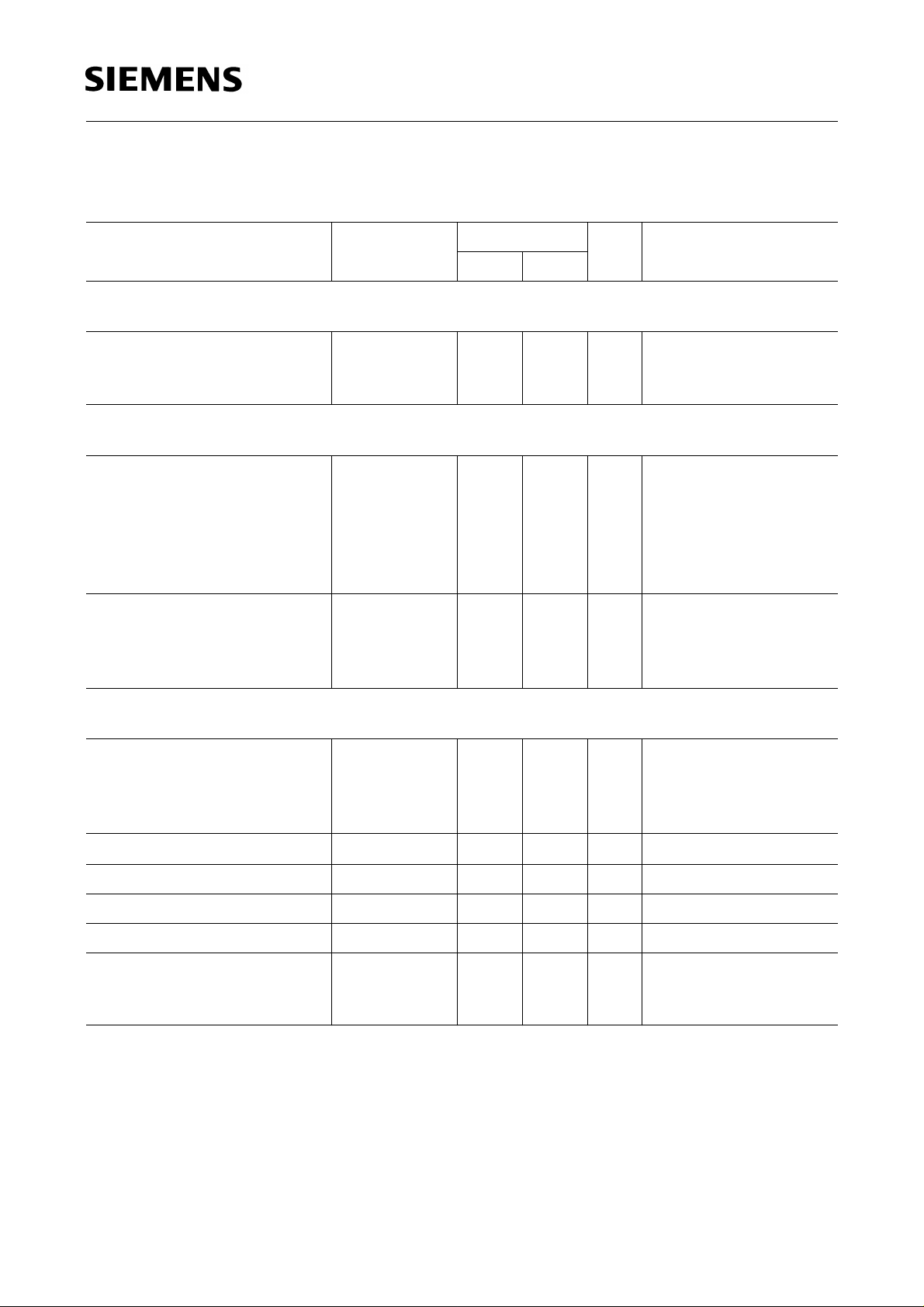
Absolute Maximum Ratings
T
= – 40 to 150 ˚C
j
Parameter Symbol Limit Values Unit Remarks
min. max.
Voltages
TLE 4226 G
Supply voltage
Supply voltage load circuit
Input voltage
Currents
Output current
Current at reverse poling
Current at reverse poling
Clamping current
Clamping current
Junction temperature
Storage temperature
Operating Range
Supply voltage V
VS
V
V
I
Q1-6
I
Q5-6
I
Q1-4
I
QZ5-6
I
QZ1-4
T
j
T
stg
V
Q1-6
IN1-6
S
S
, V
PREFST
– 1
– 0.7
– 0.7
– 500
– 50
– 40
– 55
4.75
4
10
25
20
700
70
150
125
5.25 V
V
V
V
mA
mA
mA
mA
˚C
˚C
limited internally
see diagram
Overtemperature
protection shuts down
the switches 5 and 6
at 165 ˚C
full function, but status
outputs cannot be
evaluated
Output voltage
Ambient temperature
Invert current for Q
1-6
Input voltage
in total I
V
Q
T
A
sup
V
IN
– 0.3 24 V
– 40 110 ˚C Tj≤ 150 ˚C
50 mA
– 0.5 15 V
Thermal resistance
junction to case
junction to ambient
1) Pins 5 to 8 and 17 to 20 have to be connected to the ground-plane used as thermal heatsink to achieve the
optimum thermal resistance.
R
R
th JC
th JA
15
65
K/W
K/W
1)
Semiconductor Group 6
Page 7
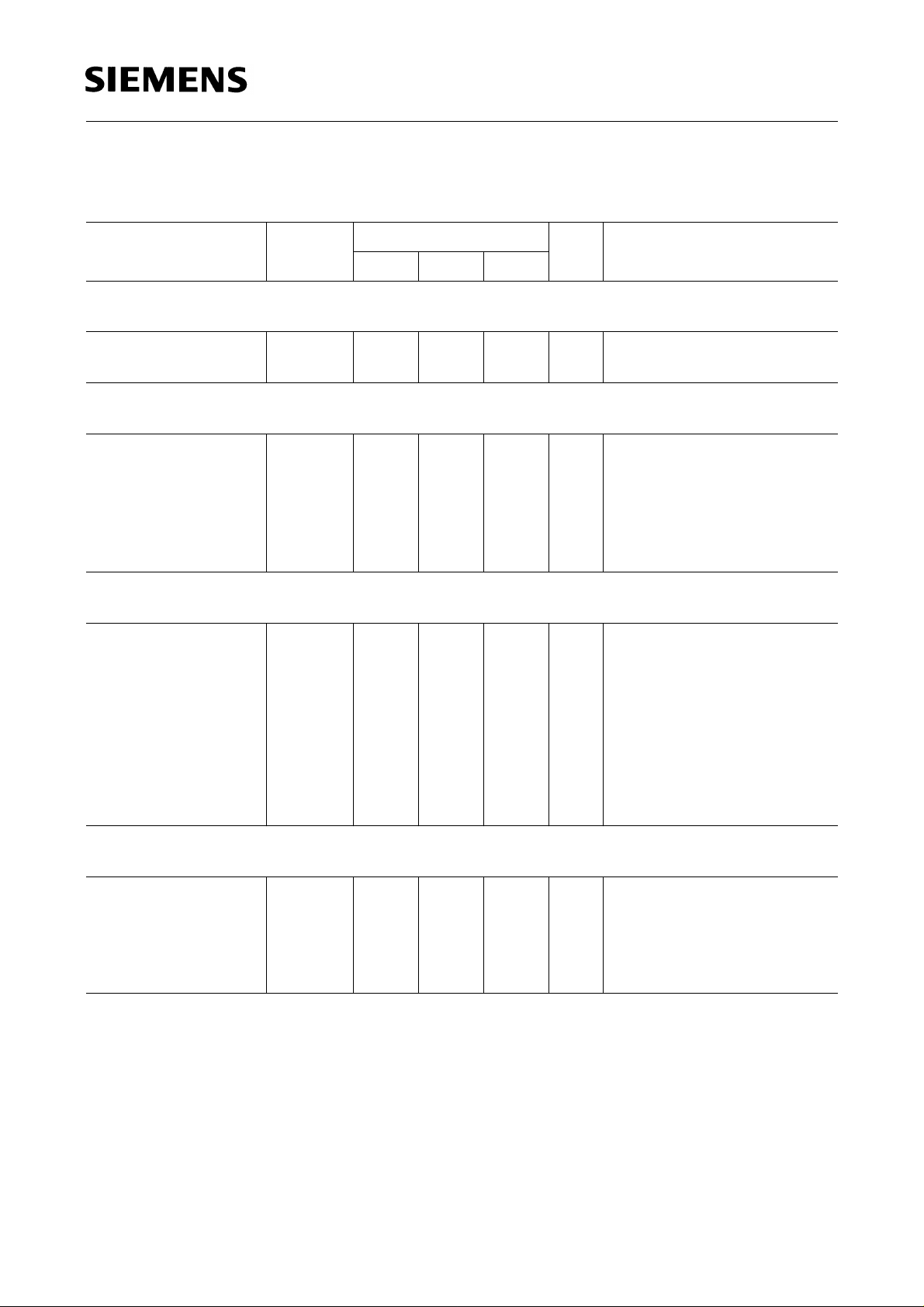
Characteristics
V
= 5 V, unless stated otherwise; Tj = – 40 to 140 ˚C
S
Parameter Symbol Limit Values Unit Test Condition
min. typ. max.
V
Supply Voltage (
Quiescent current
Supply Current
)
S
I
S
I
S
8
50
11
65
mAmAOutputs OFF
Outputs ON
Inputs (IN1-6, PREFST)
TLE 4226 G
H-input voltage
L-input voltage
Hysteresis
H-Input current
L-Input current
Input current
Power Outputs (Q1-6)
Load Current
Saturation voltage
Saturation voltage
Saturation voltage
Compare voltage
Turn-ON delay time
Turn-OFF delay time
Overtemp. Protection
Monitoring threshold
Shutdown threshold
hysteresis
V
IH
V
IL
∆V
I
IH
I
IL
I
I
I
Q1-4
V
QSat5, 6
V
QSat1-4
V
QSat1-4
V
com
t
DON
t
DOFF
T
thSt
T
tho
1.3
0.9
I
0.3
– 2
– 10
– 2
50
1.8
1.2
0.6
2.1
1.5
1.0
3
1
3
V
V
V
µA
µA
µA
mA
0.9 V < VI < 6 V
0.2 V < VI < 0.9 V
0 V < VI < 6 V; VS = 0 V
V
= 2 V and resistance from
S
PREFST to ground < 1 MΩ
4.1
0.2
0.2
150
5
0.5
0.4
1
2
155
10
0.8
0.6
0.22
4.7
1.5
3.5
V
V
V
V
µs
µs
˚C
K
I
= 0.4 A; output ON
Q
I
= 50 mA; output ON
Q
I
= 20 mA; output ON
Q
see diagrams
20 mA < I
200 mA < I
< 50 mA,
Q1-4
Q5,6
< 500 mA
only switches 5 and 6
are shut down
Reset threshold
T
thRes
140
Semiconductor Group 7
150
˚C
after shutdown
Page 8
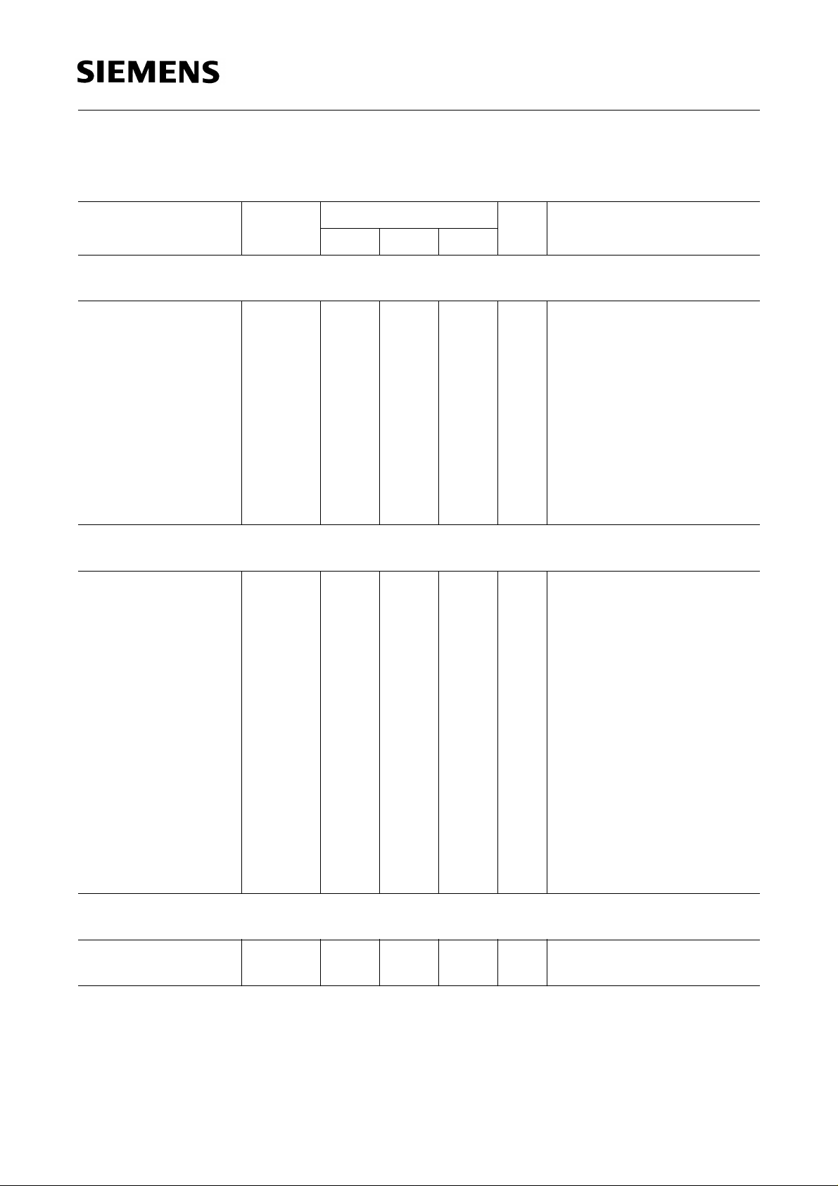
Characteristics (cont’d)
V
= 5 V, unless stated otherwise; Tj = – 40 to 140 ˚C
S
Parameter Symbol Limit Values Unit Test Condition
min. typ. max.
Outputs (Q1-6)
TLE 4226 G
Clamping voltage
Clamping voltage
Shorted load current
Shorted load current
Sink current
V
Q1-4
V
Q5, 6
I
Q1-4 max
I
Q5, 6
I
Q5, 6
Shutdown threshold
Leakage current
Leakage current
I
Q1-4
I
Q5, 6
Status Output Analog (StA)
Normal function
Error output 6
Error output 5
Overload output 4
Overload output 3
Overload output 2
Overload output 1
Thermal overload
V
StA
V
StA
V
StA
V
StA
V
StA
V
StA
V
StA
V
StA
25.5
25.5
60
500
2
1.0
1.4
1.8
2.2
2.6
3.0
3.5
33
35
170
900
10
1
200
0.5
1.3
1.7
2.1
2.5
2.9
3.3
V
V
mA
mA
µA
µA
µA
V
V
V
V
V
V
V
V
I
= 50 mA
Q
I
= 500 mA
Q
V
< 16.5 V
Q
V
≤ 10 V; Tj≤ 130 ˚C
Q
V
= 5 V
Q
switches off, VQ = 24 V
T
= 125 ˚C
j
switches off, VQ = 16.5 V
T
= 125 ˚C
j
Source resistance of
R
QStA
30
analog status output
Delay time of status
Delay time of output
t
dStA/D
t
dSQ1-6
10
10
15
protection
Status Output Digital (StD)
Pull-up resistance
Saturation voltage
R
V
StD
StDSat
10 20 30
Semiconductor Group 8
250
30
30
0.4
Ω
µs
µs
kΩ
V I
– I
= 50 ... 100 µA
QStA
overload at switches 5 and 6
switches 5 and 6 during turn
on
= 4 mA
StD
Page 9
TLE 4226 G
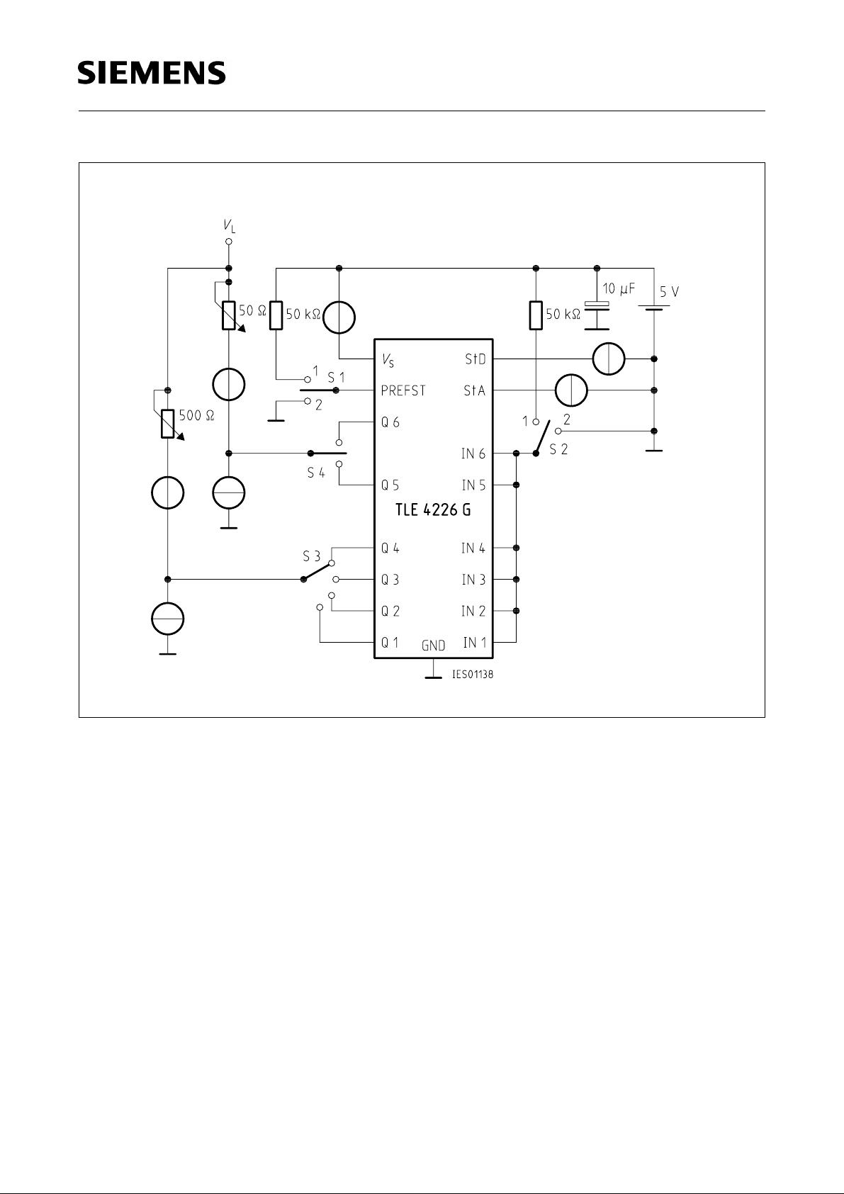
Test Circuit
S1 in position 1: all outputs can be activated (position 1) or deactivated (position 2) by S2
S1 in position 2: preferred state
Semiconductor Group 9
Page 10
TLE 4226 G
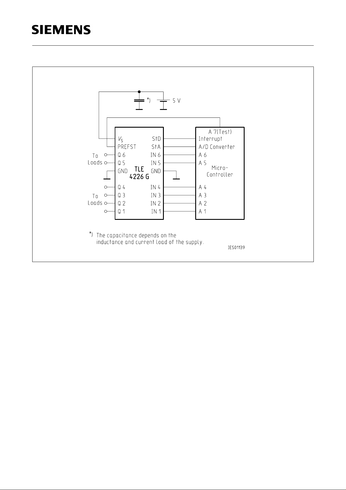
Application Circuit
*) The capacitance depends on the inductance and current load of the supply.
Semiconductor Group 10
Page 11
TLE 4226 G
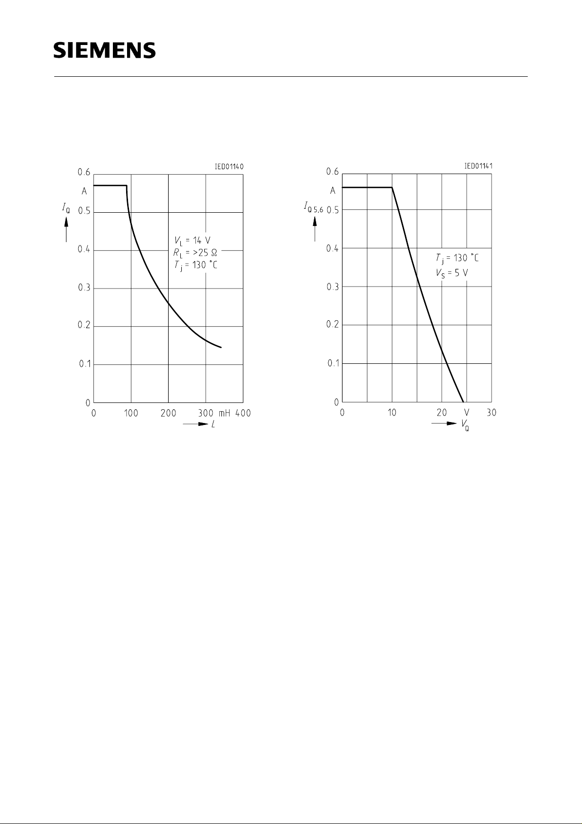
Permissible Load Inductance versus Load
Current
Shorted Load Current I
Q5, 6
Voltage (Outputs 5 and 6)
versus Output
Note:
T
While switching the maximum inductive loads, the maximum temperature
The IC will not be destroyed by this, but the restrictions concerning useful life should be observed.
of 150 ˚C may be briefly exceeded.
j
Semiconductor Group 11
Page 12
TLE 4226 G
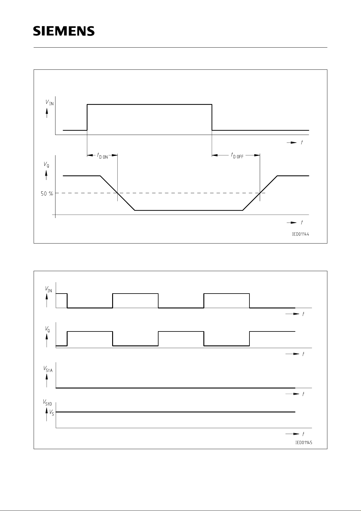
Timing Diagrams
Signals of Inputs and Outputs of Switches 1 to 6
Normal Function (no Error)
Semiconductor Group 12
Page 13
TLE 4226 G
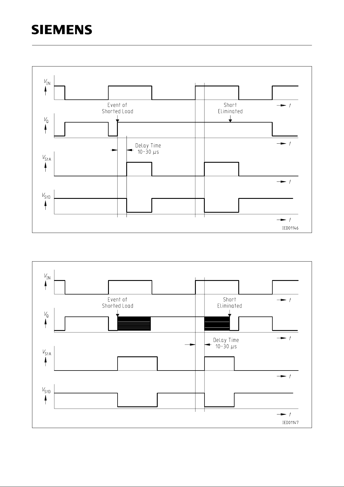
Signals of Inputs and Outputs of Switches 1 to 4
Shorted Load to Supply Voltage of Load Circuit
Signals of Inputs and Outputs of Switches 5 and 6
Shorted Load to Supply Voltage of Load Circuit
Semiconductor Group 13
Page 14
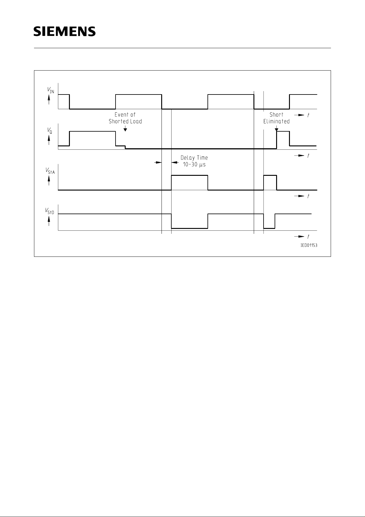
TLE 4226 G
Signals of Inputs and Outputs of Switches 5 and 6
Shorted Load to Ground
Semiconductor Group 14
Page 15
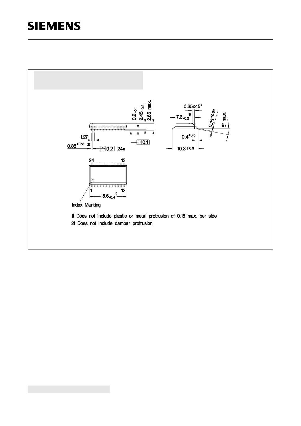
Package Outlines
P-DSO-24-3
(Plastic Dual Small Outline Package)
TLE 4226 G
Sorts of Packing
Package outlines for tubes, trays etc. are contained in our
Data Book “Package Information”.
SMD = Surface Mounted Device
GPS05144
Dimensions in mm
Semiconductor Group 15
 Loading...