

Page 1

Data sheet, Rev. 1.0, July 2007
现货库存、技术资料、百科信息、热点资讯,精彩尽在鼎好!
TLE4250-2
Low Dropout Voltage Tracking Regulator
Automotive Power
Page 2
Low Dropout Voltage Tracking Regulator TLE4250-2
1Overview
Features
• 50 mA Output Current Capability
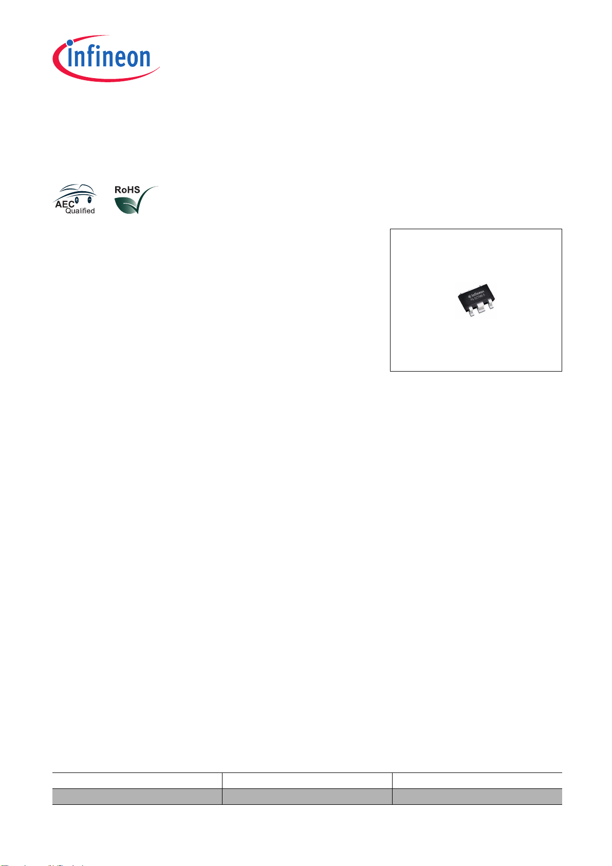
• Tiny SMD-Package PG-SCT595-5 with lowest
thermal resistance
• Low Output Tracking Tolerance
• Stable with Small Ceramic Output Capacitor
• Low Dropout Voltage
• Combined Reference / Enable Input
• Low Current Consumption in Stand-by Mode
• Maximum Input Voltage -42 V ≤
V
≤ +45 V
I
• Reverse Polarity Protection
• Output Short Circuit Proof to Ground and Supply
• Overtemperature Protection
• Temperature Range -40 °C ≤
T
≤ 150 °C
j
• Green Product (RoHS compliant)
• AEC Qualified
PG-SCT595-5
Functional Description
The TLE4250-2 is a monolithic integrated low dropout voltage tracker in a tiny SMD package PG-SCT595-5 with
excellent thermal resistance. It is designed to supply off-board loads (e.g. sensors) in automotive environment.
The IC protects itself in case of overload, overtemperature, reverse polarity as well as output short circuit to battery
and ground.
Supply voltages up to
V
= 45 V are regulated to a reference voltage applied at the adjust input “ADJ” with high
I
accuracy. The output “Q” is able to drive loads up to 50 mA.
In order to reduce the quiescent current to a minimum, the TLE4250-2 can be switched to stand-by mode by
setting the adjust/enable input “ADJ/EN” to “low”.
Type Package Marking
TLE4250-2G PG-SCT595-5 52
Data sheet 2 Rev. 1.0, 2007-07-24
Page 3
2 Block Diagram
TLE4250-2
Block Diagram
Volt a ge
divider
optional
Supply
C
I
Reference
I
ADJ/ EN
ADJ/EN
Bl ockDi agram.vsd
Internal
Supply
TLE 4250-2
Saturation Control
Current Limit ation
Temp.
Protection
GND
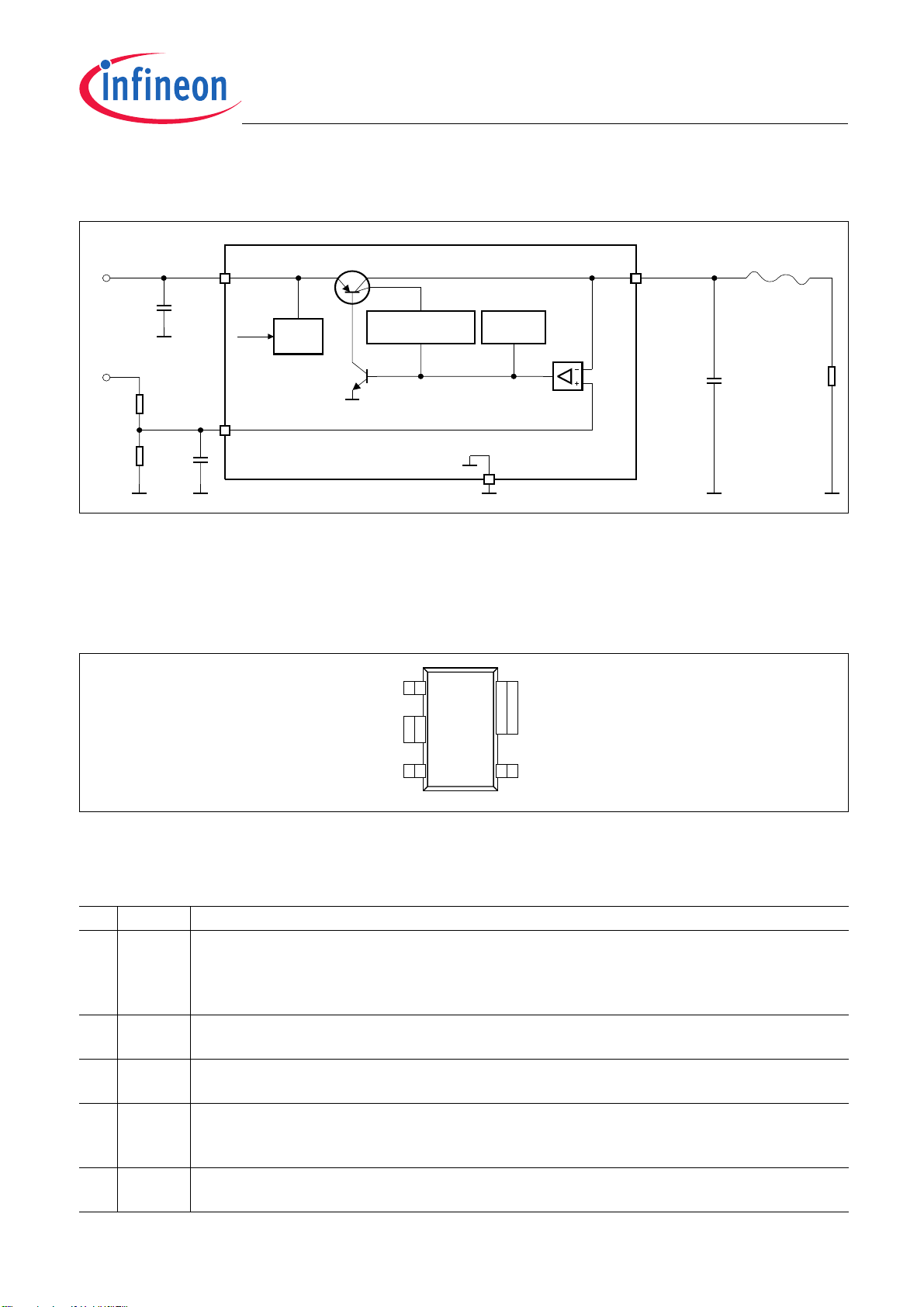
Figure 1 Block Diagram and Simplified Typical Application
3 Pin Configuration
3.1 Pin Assignment
ADJ /EN
GND
1
5
2
GND
Q
Regulated
Output Voltage
C
Q
off-board
load
I
Figure 2 Pin Configuration Package PG-SCT595-5
3.2 Pin Definitions and Functions
Pin Symbol Function
1ADJ/ENAdjust / Enable.
Connect the reference to this pin. A low signal disables the IC; a high signal switches it on.
The reference voltage can be connected directly or by a voltage divider for lower output voltages.
For compensating line influences, a capacitor close to the IC pins is recommended.
2GND Ground Reference.
Internally connected to Pin 5. Connect to heatsink area.
3I Input.
IC supply. For compensating line influences, a capacitor close to the IC pins is recommended.
4Q Tracker Output.
Block to GND with a capacitor close to the IC terminals, respecting capacitance and ESR
requirements given in the table “Functional Range”.
5GND Ground Reference.
Internally connected to Pin 2. Connect to heatsink area.
43
Pinout.vsd
Q
Data sheet 3 Rev. 1.0, 2007-07-24
Page 4
4 General Product Characteristics
4.1 Absolute Maximum Ratings
TLE4250-2
General Product Characteristics
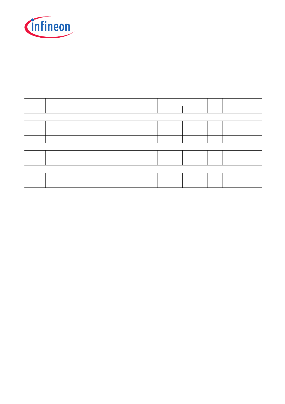
Absolute Maximum Ratings
1)
-40 °C ≤ Tj ≤ 150 °C; all voltages with respect to ground (unless otherwise specified).
Pos. Parameter Symbol Limit Values Unit Conditions
Min. Max.
Voltages
4.1.1 Input voltage
4.1.2 Output voltage
4.1.3 Adjust / Enable Input
V
I
V
Q
V
ADJ/EN
-42 45 V –
-1 40 V –
-0.3 40 V –
Temperatures
4.1.4 Junction Temperature
4.1.5 Storage Temperature
T
j
T
stg
-40 150 °C–
-50 150 °C–
ESD Susceptibility
4.1.6 ESD Resistivity
4.1.7 V
1) Not subject to production test, specified by design.
2) ESD susceptibility, Human Body Model “HBM” according to EIA/JESD 22-A114B
3) ESD susceptibility, Charged Device Model “CDM” according to EIA/JESD22-C101 or ESDA STM5.3.1
V
ESD,HBM
ESD,CDM
-3 3 kV HBM
-2 2 kV CDM
2)
3)
Note: Stresses above the ones listed here may cause permanent damage to the device. Exposure to absolute
maximum rating conditions for extended periods may affect device reliability.
Note: Integrated protection functions are designed to prevent IC destruction under fault conditions described in the
data sheet. Fault conditions are considered as “outside” normal operating range. Protection functions are
not designed for continuous repetitive operation.
Data sheet 4 Rev. 1.0, 2007-07-24
Page 5
TLE4250-2
General Product Characteristics
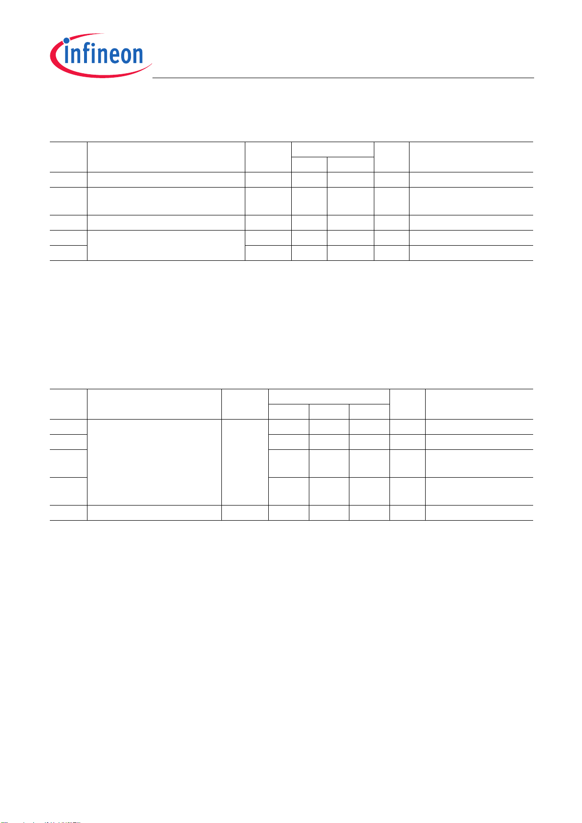
4.2 Functional Range
Pos. Parameter Symbol Limit Values Unit Conditions
Min. Max.
4.2.1 Input Voltage
4.2.1 Adjust / Enable Input Voltage
(Voltage Tracking Range)
4.2.2 Junction Temperature
4.2.3 Output Capacitor Requirements
4.2.4 ESR
1) The minimum output capacitance requirement is applicable for a worst case capacitance tolerance of 30%
2) relevant ESR value at f = 10 kHz
Note: Within the functional range the IC operates as described in the circuit description. The electrical
characteristics are specified within the conditions given in the related electrical characteristics table.
V
I
V
ADJ/EN
T
j
C
Q
440 V–
2.5 36 V –
-40 150 °C–
1– µF–
–3 Ω –
CQ
1)
2)
4.3 Thermal Resistance
Pos. Parameter Symbol Limit Value Unit Conditions
Min. Typ. Max.
4.3.5 Junction to Ambient
R
thJA
– 81 – K/W 2s2p board
4.3.1 – 217 – K/W Footprint only
4.3.2 – 117 – K/W 300 mm2 PCB heatsink
2)
area
4.3.3 – 103 – K/W 600 mm2 PCB heatsink
2)
area
4.3.4 Junction to Soldering Point R
1) Specified R
(chip+package) was simulated on a 76.2 x 114.3 x 1.5 mm board with 2 inner copper layers (2 x 70µm Cu, 2 x 35µm Cu).
Where applicable a thermal via array under the package contacted the first inner copper layer.
2) Package mounted on PCB FR4; 80 x 80 x 1.5 mm; 35 µm Cu, 5 µm Sn; horizontal position; zero airflow.
Not subject to production test; specified by design.
value is according to JESD51-2,-5,-7 at natural convection on FR4 2s2p board; The product
thJA
thJSP
– 30 – K/W Pins 2, 5 fixed to T
1)
2)
A
Data sheet 5 Rev. 1.0, 2007-07-24
Page 6
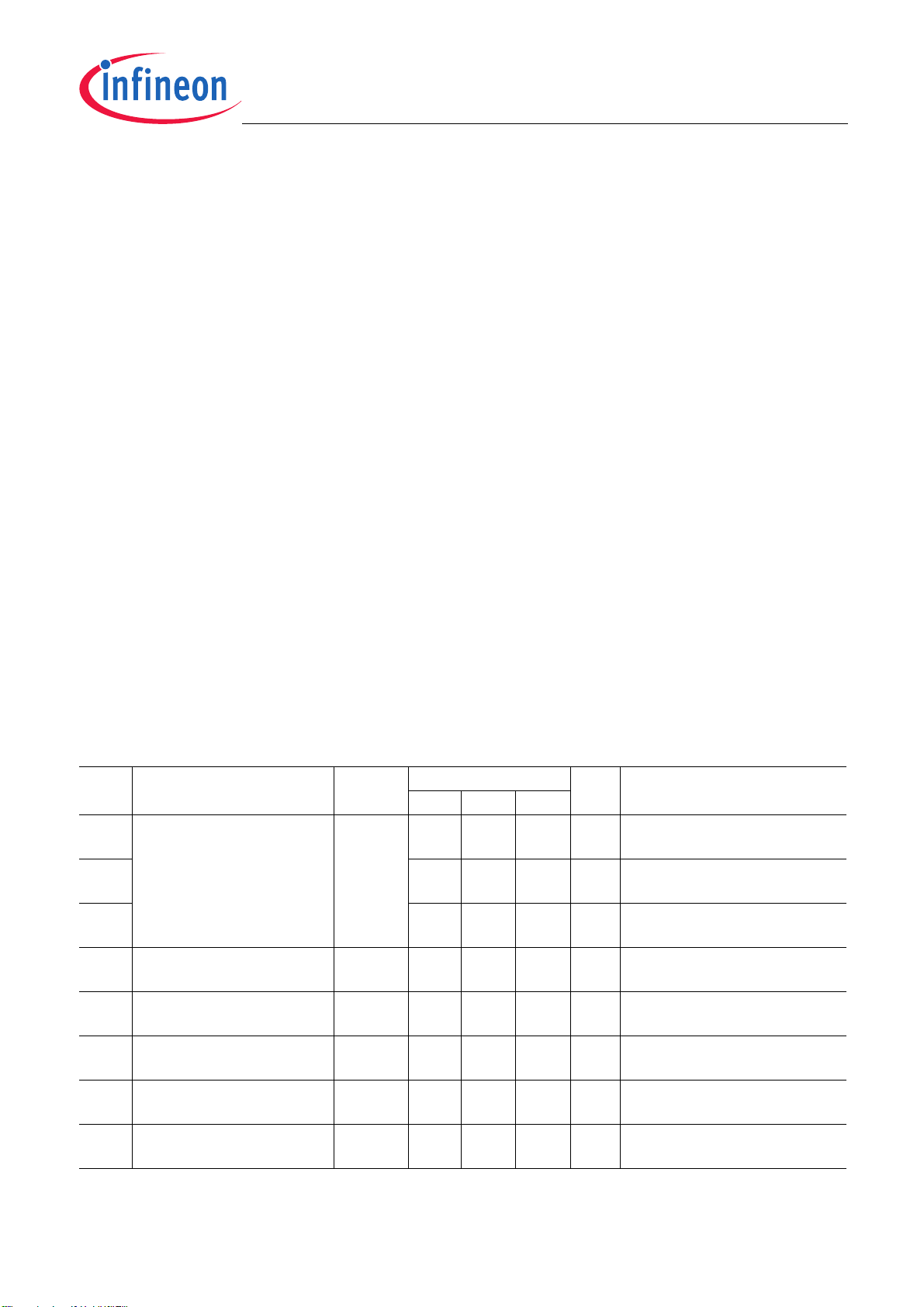
TLE4250-2
Electrical Characteristics
5 Electrical Characteristics
5.1 Tracking Regulator
The output voltage VQ is controlled by comparing it to the voltage applied at pin ADJ/EN and driving a PNP pass
transistor accordingly. The control loop stability depends on the output capacitor
temperature and the poles/zeros introduced by the integrated circuit. To ensure stable operation, the output
capacitor’s capacitance and its equivalent series resistor ESR requirements given in the table “Functional Range”
have to be maintained. For details see also the typical performance graph “Output Capacitor Series Resistor
ESR
vs. Output Current IQ”. Also, the output capacitor shall be sized to buffer load transients.
CQ
An input capacitor
C
is recommended to buffer line influences. Connect the capacitors close to the IC terminals.
I
Protection circuitry prevent the IC as well as the application from destruction in case of catastrophic events. These
safeguards contain output current limitation, reverse polarity protection as well as thermal shutdown in case of
overtemperature.
In order to avoid excessive power dissipation that could never be handled by the pass element and the package,
the maximum output current is decreased at high input voltages.
The overtemperature protection circuit prevents the IC from immediate destruction under fault conditions (e. g.
output continuously short-circuited) by reducing the output current. A thermal balance below 200 °C junction
temperature is established. Please note that a junction temperature above 150 °C is outside the maximum ratings
and reduces the IC lifetime.
The TLE4250-2 allows a negative supply voltage. However, several small currents are flowing into the IC. For
details see electrical characteristics table and typical performance graphs. The thermal protection circuit is not
operating during reverse polarity condition.
C
, the load current, the chip
Q
Table 1 Electrical Characteristics Tracking Regulator
V
= 13.5 V; V
I
≥ 2.5 V; -40 °C ≤ Tj ≤ 150 °C; all voltages with respect to ground (unless otherwise specified).
ADJ/EN
Pos. Parameter Symbol Limit Values Unit Conditions
Min. Typ. Max.
5.1.1 Output Voltage Tracking
Accuracy
5.1.2 -25 – 25 mV 1 mA ≤
5.1.3 -25 – 25 mV 1 mA ≤
5.1.4 Load Regulation
∆
|d
V
Q
-5 – 5 mV 1 mA ≤ IQ ≤ 10 mA;
6 V ≤
6 V ≤
6 V ≤
V
|– – 15 mV IQ = 1 mA to 30 mA;
Q,load
V
≤ 16 V
I
I
≤ 50 mA;
Q
V
≤ 28 V
I
I
≤ 10 mA;
Q
V
≤ 40V
I
steady-state
5.1.5 Line Regulation
steady-state
5.1.6 Power Supply Ripple
Rejection
5.1.7 Dropout Voltage
V
= VI - V
dr
Q
5.1.8 Output Current Limitation
|d
V
Q,line
PSRR
V
dr
I
Q,max
|– – 10 mV VI = 6 V to 40 V;
I
= 10 mA
Q
–48– dBf
= 100 Hz;
ripple
V
ripple
= 1 Vpp
– 100 300 mV IQ = 10 mA
V
≥ 4 V 2)
ADJ
51 85 120 mA VQ = (V
ADJ
1)
- 0.1 V)
Data sheet 6 Rev. 1.0, 2007-07-24
Page 7
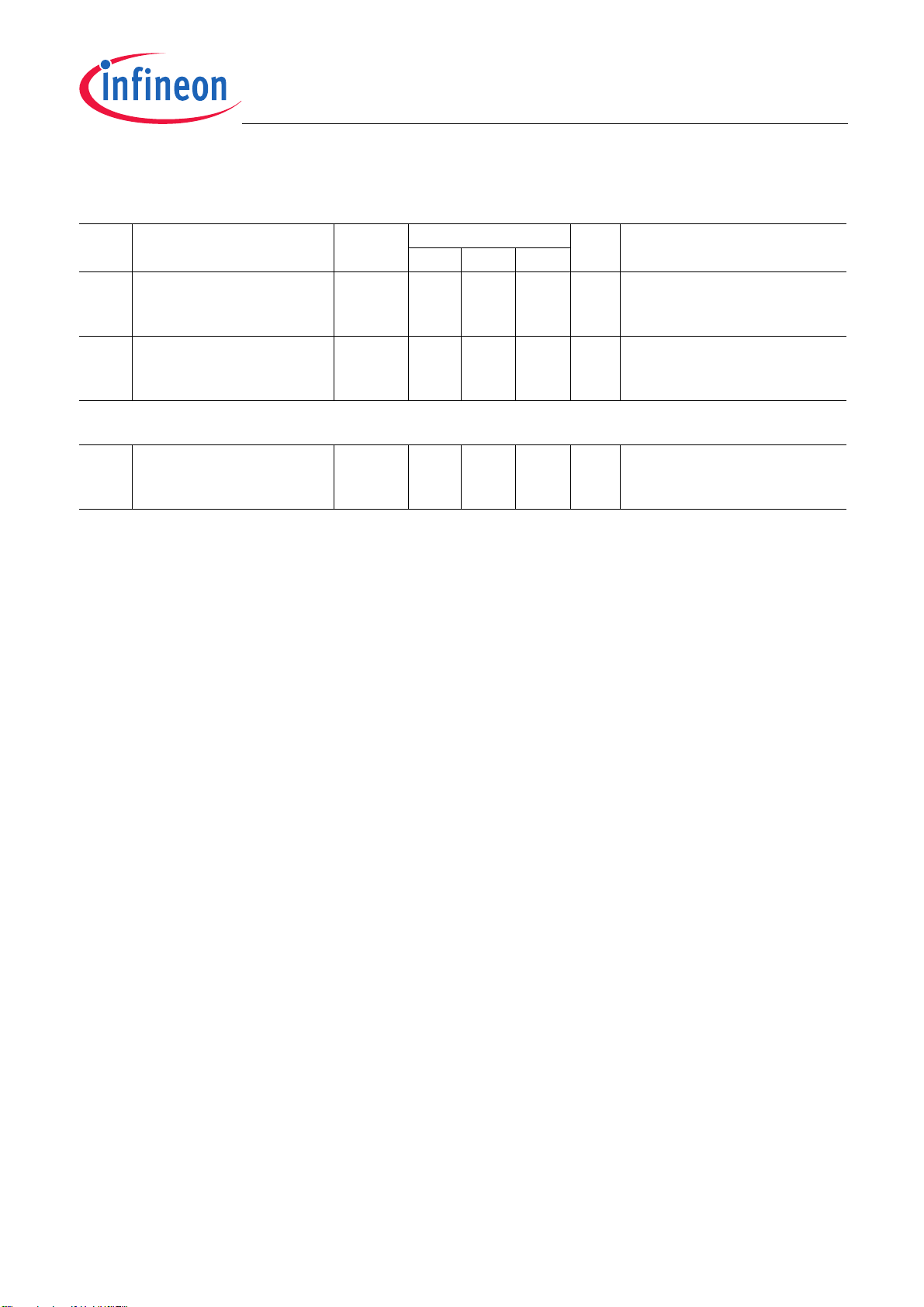
Electrical Characteristics
Table 1 Electrical Characteristics Tracking Regulator
V
= 13.5 V; V
I
≥ 2.5 V; -40 °C ≤ Tj ≤ 150 °C; all voltages with respect to ground (unless otherwise specified).
ADJ/EN
Pos. Parameter Symbol Limit Values Unit Conditions
Min. Typ. Max.
5.1.9 Reverse Current I
5.1.10 Reverse Current
at Negative Input Voltage
Q
I
I
-5 -1 – mA VI = 0 V;
V
= 16 V;
Q
V
= 5 V
ADJ
-10 -2 – mA VI = -16 V;
V
= 0 V;
Q
V
= 5 V
ADJ
Overtemperature Protection:
5.1.11 Junction Temperature
Equilibrium
1) Parameter not subject to production test; specified by design.
2) Measured when the output voltage
T
j,eq
V
has dropped 100 mV from its nominal value.
Q
151 – 200 °C Tj increasing due to power
dissipation generated
by the IC
1)
TLE4250-2
Data sheet 7 Rev. 1.0, 2007-07-24
Page 8
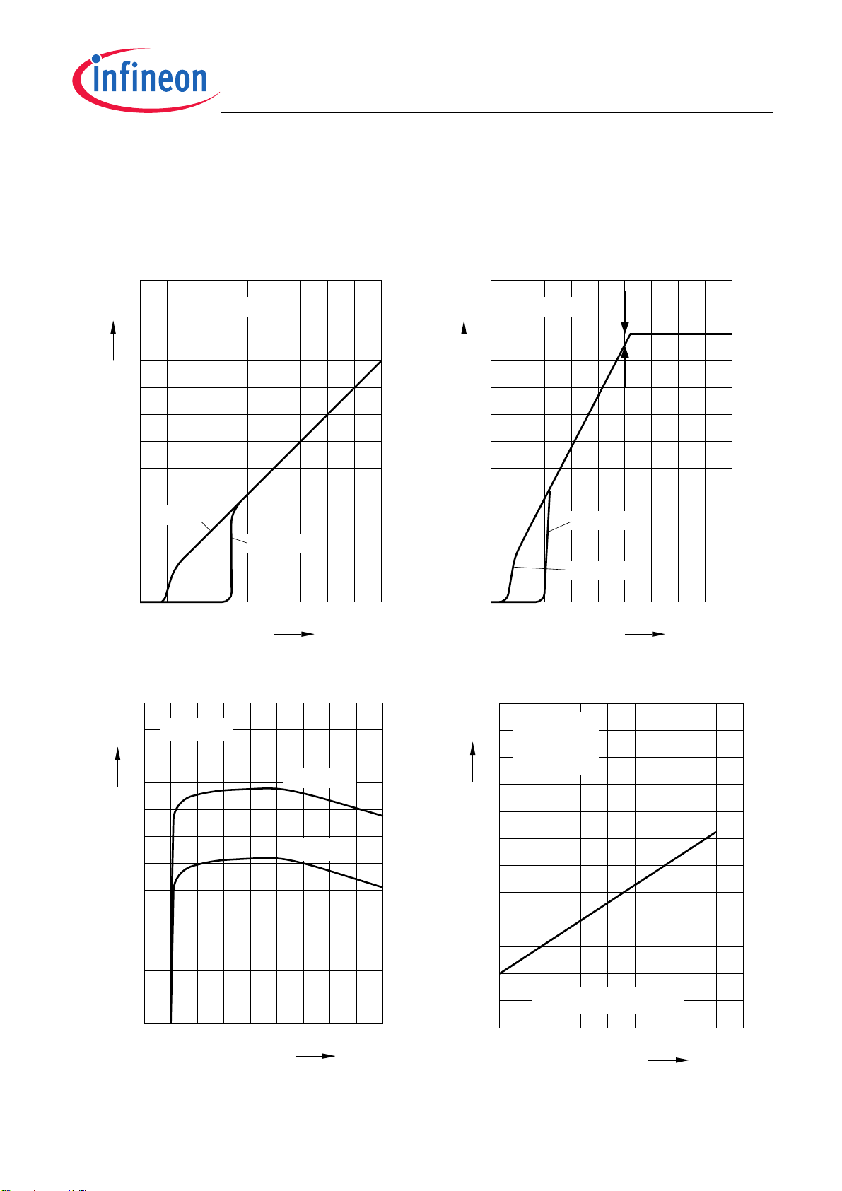
Typical Performance Characteristics Tracking Regulator
V
= 5 V (unless otherwise noted)
ADJ/EN
TLE4250-2
Electrical Characteristics
Output Voltage
Adjust Voltage
V
[V]
Q
4
3
2
T
= 150 °C
j
1
V
Q
V
ADJ
V
1
vs.
= 13. 5 V
I
VQ-VADJ.vsd
T
= -40 °C
j
234
V
[V]
ADJ
Output Voltage
Input Voltage
V
Q
[V]
V
4
3
2
1
1
V
vs.
Q
V
I
= 13.5 V
I
T
= -40 °C
j
T
= 150 °C
j
3
VQ-VI.v sd
V
dr
57
V
[V]
I
Maximum Output Current IQ vs.
Input Voltage
V
I
120
V
I
Q
[mA]
ADJ
= 5 V
80
60
40
20
0
10 40
20 30
Tj = 25 °C
Tj = 125 °C
V
SOA.VSD
[V]
I
Line Regulation d
V
Q,line
Input Voltage Change d
∆
V
[mV]
Q
0.3
0.2
0.1
V
= 6 V
I,initial
V
= 5 V
ADJ
I
= 5 mA
Q
0
steady-state condition
5 1520 3035
0
10 25
vs.
V
)
I
∆
V
dVQ -dVI.vs d
40
[V]
I
Data sheet 8 Rev. 1.0, 2007-07-24
Page 9
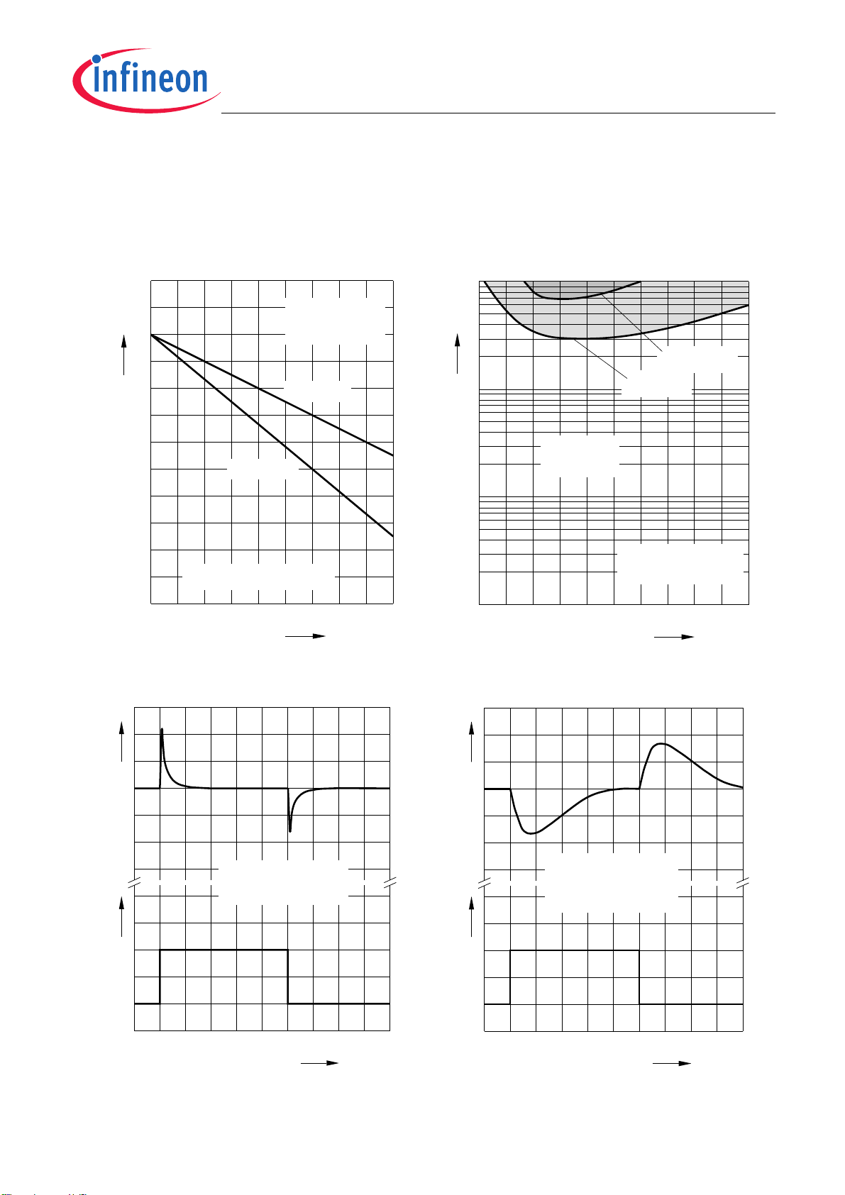
Typical Performance Characteristics Tracking Regulator
V
= 5 V (unless otherwise noted)
ADJ/EN
TLE4250-2
Electrical Characteristics
Load Regulation d
V
Q,line
Output Current Change d
∆
V
[mV]
Q
-2
-4
T
-6
-8
steady-state condition
0
12
vs.
I
Q
I
Q ,init ial
V
= 5 V
ADJ
T
= 25 °C
j
= 125 °C
j
24 36 48
dVQ -dIQ.vs d
= 1 mA
∆Ι
Q
[mA]
Output Capacitor Series Resistor
vs. Output Current
10
ESR
CQ
[Ω]
1
0.1
0.01
0
I
Q
C
Q
Stable
Region
V
< 28 V
I
-40 °C <
10 40
20 30
ESR
C
Q
= 1 µF
T
CQ
ESR-IQ .vsd
= 2.2 µF
< 150 °C
j
I
[mA]
Q
50
Line Transient Response Load Transient Response
dVI -reponse.vsd
∆
V
[mV]
V
[V]
Q
-20
-40
I
16
0
I
= 5 mA
Q
C
= 2.2 µF C eram ic
Q
9
0
20 80
40 60
t
[µs]
∆
V
[mV]
Ι
[mA]
Q
0
-50
V
= 13.5 V
I
V
= 5 V
AD J
C
= 2.2 µF Ceram ic
Q
Q
30
5
0
20 80
40 60
dIQrespons e.vsd
t
[µs]
Data sheet 9 Rev. 1.0, 2007-07-24
Page 10
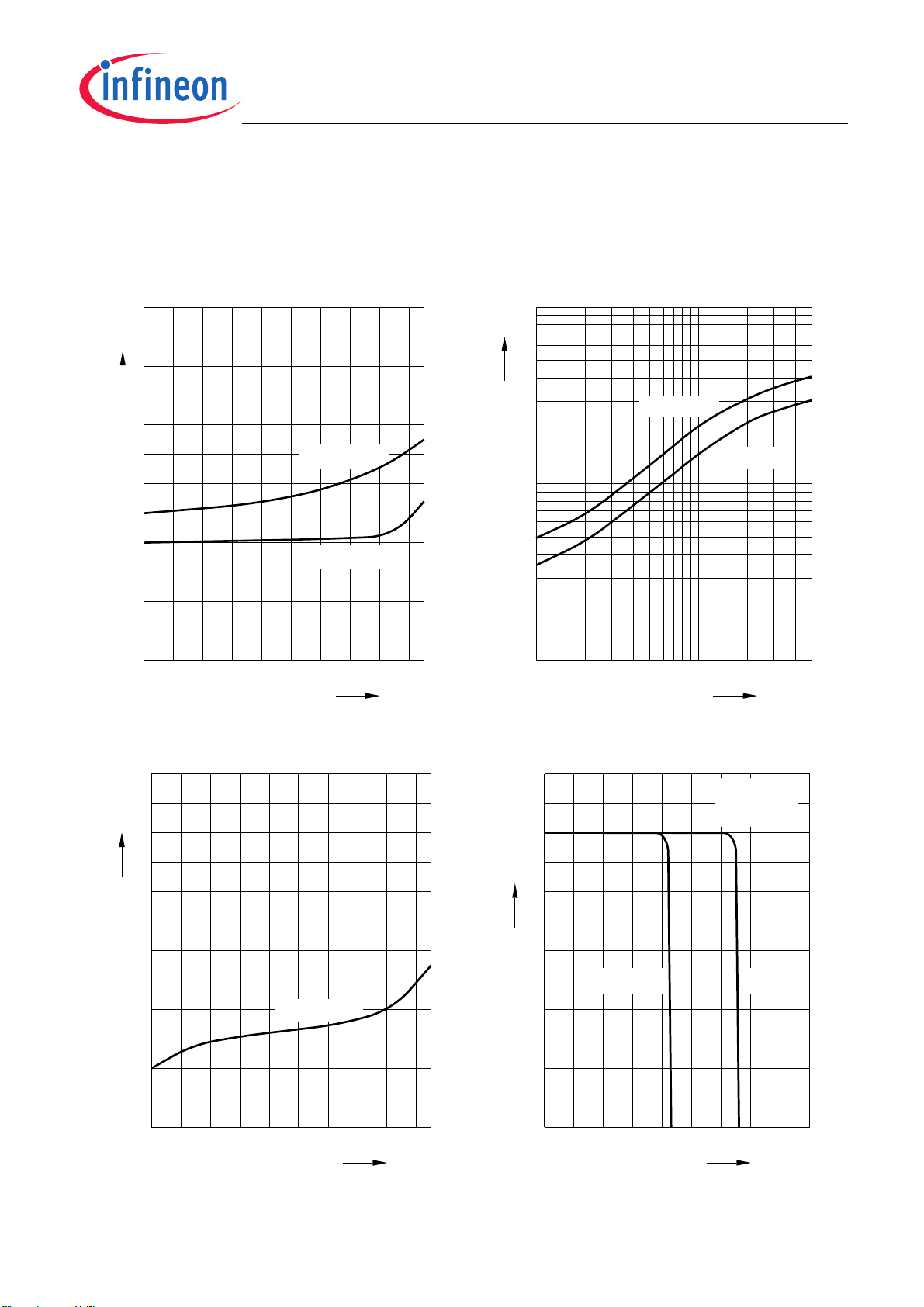
Typical Performance Characteristics Tracking Regulator
V
= 5 V (unless otherwise noted)
ADJ/EN
TLE4250-2
Electrical Characteristics
Tracking Accuracy ∆
V
Junction Temperature
∆
V
Q
[mV]
8
4
0
-4
-20 20 40 80 100
-40
0 60 140120
vs.
Q
T
V
Dropout Voltage
j
I
= 50 mA
Q
dVQ-Tj.v sd
Output Current
V
[mV]
dr
vs.
dr
I
Q
T
= 150 °C
j
T
= 25 ° C
j
V dr-IQ_l og.v sd
100
I
= 1 mA
Q
10
110
T
[°C]
j
50
I
[mA]
Q
Dropout Voltage Vdr vs.
Junction Temperature
V
[mV]
dr
250
200
150
100
0 60 140120
-20 20 40 80 100
-40
T
j
I
= 10 m A
Q
T
V dr-Tj.v sd
[°C]
j
Output Current Limitation I
vs. Output Voltage
V
Q
5
V
[V]
Q
3
Tj = 125° C Tj = 25°C
2
1
0
20
40
60
Q,max
VI = 13.5 V
= 5 V
V
ADJ
80 100
IQmax-VQ.vsd
[mA]
I
Q
Data sheet 10 Rev. 1.0, 2007-07-24
Page 11
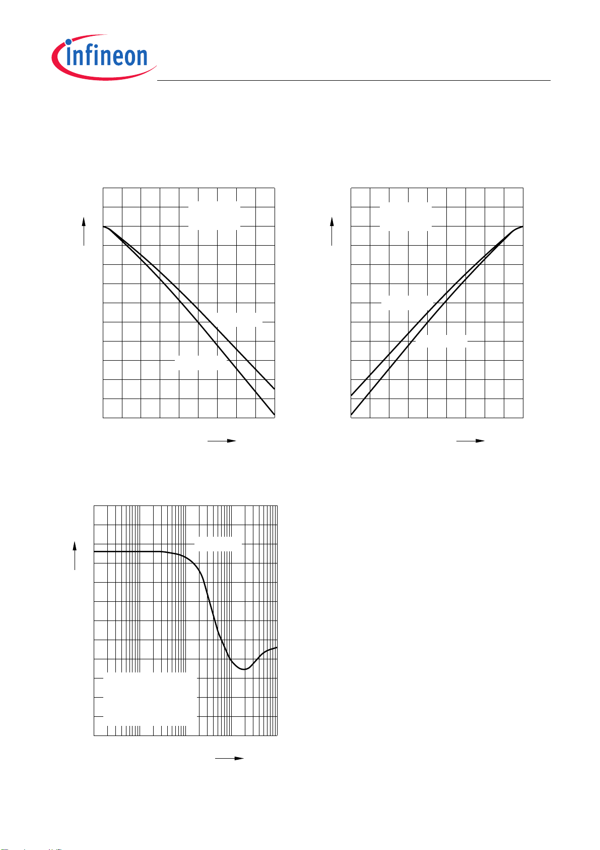
Typical Performance Characteristics Tracking Regulator
V
= 5 V (unless otherwise noted)
ADJ/EN
TLE4250-2
Electrical Characteristics
Reverse Output Current
Output Voltage
+0.5
I
[mA]
Q
-0.5
-1
-1.5
-2
V
Q
0
832
I
vs.
Q
V
= 0 V
I
V
ADJ
T
= 150 °C
j
16 24
= 5 V
T
= -40 °C
j
I
vs.
I
V
I
V
= 0 V
Q
V
= 5 V
ADJ
II-VI.vsd
IQ-VQ.vsd
Reverse Current
Input Voltage
+0.5
I
[mA]
I
-0.5
T
-1
-1.5
= -40 °C
j
T
= 150 °C
j
-2
-32
V
[V]
Q
-24 0
-16 -8
V
[V]
I
Power Supply
Ripple Rejection
60
PSRR
[dB]
40
30
20
V
RIPPLE
V
= 13.5 V
0.01
IN
C
= 2.2 µF Ceramic
Q
T
= 25 °C
j
10
PSRR
PSR R.vsd
I
= 5 m A
Q
= 1 V
0.1 1 100
10
f
[kHz]
Data sheet 11 Rev. 1.0, 2007-07-24
Page 12
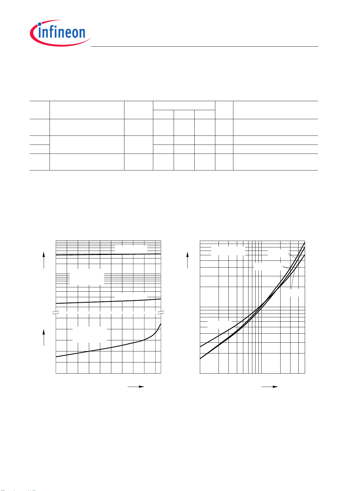
Electrical Characteristics
5.2 Current Consumption
Table 2 Electrical Characteristics Current Consumption
V
= 13.5 V; V
I
Pos. Parameter Symbol Limit Values Unit Conditions
5.2.1 Quiescent Current
Stand-by Mode
5.2.2 Current Consumption
I
= II - I
5.2.3 – 3 5 mA
q
5.2.4 Current Consumption
Dropout Region;
Typical Performance Characteristics Current Consumption
V
= 5 V (unless otherwise noted)
ADJ/EN
≥ 2.5 V; -40 °C ≤ Tj ≤ 150 °C; all voltages with respect to ground (unless otherwise specified).
ADJ/EN
Min. Typ. Max.
I
q1
I
q2
Q
I
q3
I
= II - I
q
Q
–1020µAV
T
≤ 0.4 V;
ADJ/EN
≤ 85 °C
j
– 140 200 µA IQ ≤ 1 mA;
I
≤ 30 mA;
Q
–12mAV
= VI = 5 V;
ADJ
I
= 0 mA
Q
TLE4250-2
Current Consumption
I
q1
vs. Junction Temperature
I
[mA]
q2
V
= 13.5V
I
V
= 5 V
EN/ADJ
V
= 13.5V
I
V
= 0 V
EN/ADJ
-20 20 40 80 100
060 140120
I
q1
1
0.1
[µA]
16
12
-40
, Iq2
T
I
= 5 V
q2
vs.
V
= 13.5 V
I
V
= 9 V
I
V
I
Iq-IQ.vsd
= 32 V
Current Consumption
j
I
= 30 mA
Q
I
= 1 mA
Q
Iq-Tj.vsd
Output Current
I
[mA]
q
V
I
Q
EN/ADJ
1
V
= 32 V
I
T
[°C]
j
0.1
110
I
Q
50
[mA]
Data sheet 12 Rev. 1.0, 2007-07-24
Page 13
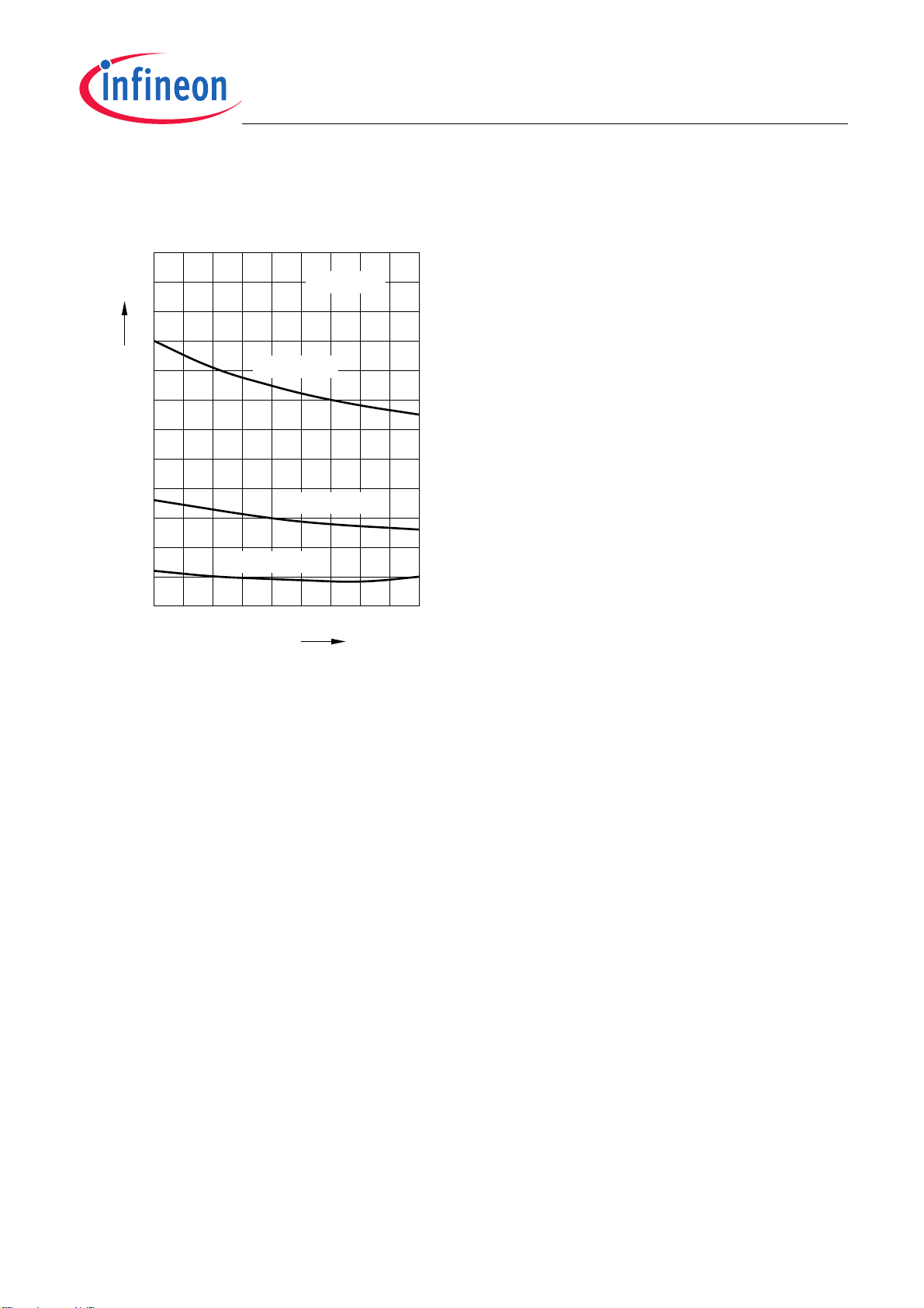
Current Consumption Iq2 vs.
Input Voltage
12
I
[mA]
q
V
I
I
8
= 50 m A
Q
6
TLE4250-2
Electrical Characteristics
Iq-VI.vsd
V
= 5 V
ADJ
4
I
= 30 mA
Q
2
6
I
= 10 m A
Q
10 22
14 18
V
[V]
I
24
Data sheet 13 Rev. 1.0, 2007-07-24
Page 14
TLE4250-2
Electrical Characteristics
5.3 Adjust / Enable Input
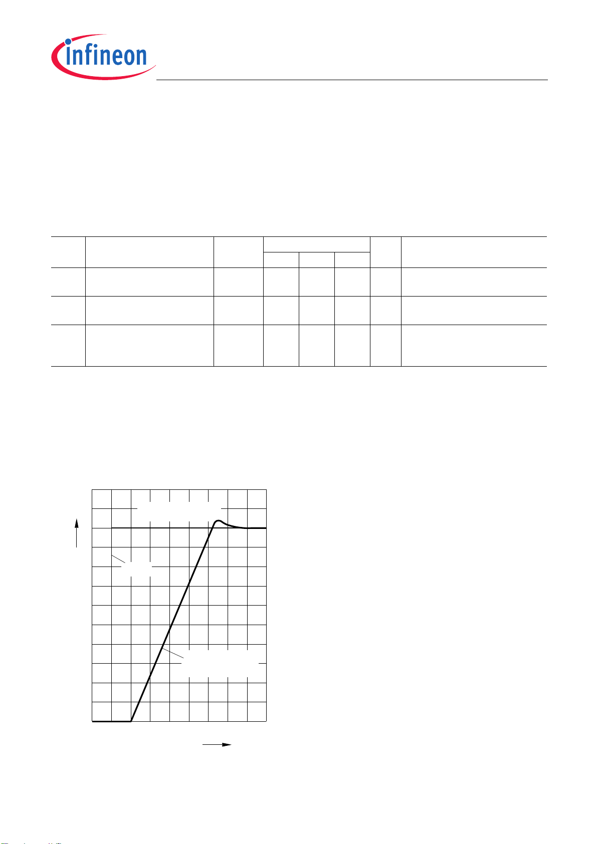
In order to reduce the quiescent current to a minimum, the TLE4250-2G can be switched to stand-by mode by
setting the adjust/enable input “ADJ/EN” to “low”.
Table 3 Electrical Characteristics Adjust / Enable
V
= 13.5 V; V
I
all voltages with respect to ground, positive current flowing into pin (unless otherwise specified).
Pos. Parameter Symbol Limit Values Unit Conditions
5.3.1 Adjust / Enable
Input Current
5.3.2 Adjust / Enable
Low Signal Valid
5.3.3 Adjust / Enable
High Signal Valid
(Tracking Region)
≥ 2.5 V; -40 °C ≤ Tj ≤ 150 °C;
ADJ
I
ADJ
V
ADJ,low
V
ADJ,high
Min. Typ. Max.
–0.10.5µAV
ADJ
= 5 V;
––0.4VVQ = 0 V;
2.5 – 36 V |VQ - V
ADJ
| < 25 mV;
Typical Performance Characteristics Adjust / Enable Input
VADJ/EN = 5V (unless otherwise noted)
Startup Sequence
4250-2_startup.v sd
V
[V]
4
3
2
1
Overshoot depends on
load current, C
V
ADJ
Q
d
(
, ESR
I
V
Q
Q,max
CQ
/ dt =
-
I
Load
) /
C
Q
20 60 80 120 140
0
40 100
t
[µs]
Data sheet 14 Rev. 1.0, 2007-07-24
Page 15
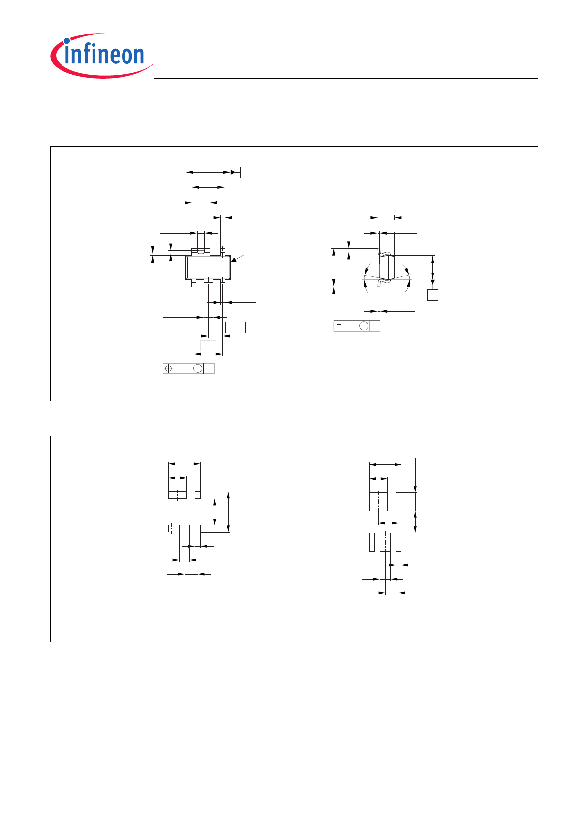
5 Package Outlines
±0.2
2.9
(2.2)
+0.1
1.2
-0.05
1)
(0.4)
1)
(0.13)
(0.23)
+0.1
0.6
-0.05
B
(0.3)
+0.2
acc. to DIN 6784
34521
+0.1
0.3
-0.05
0.95
±0.1
2.5
1.1 MAX.
±0.1
0.25
10˚ MAX.
0.2MA
0.1 MAX.
+0.1
0.15
-0.06
±0.1
1.6
10˚ MAX.
A
TLE4250-2
Package Outlines
M
0.25
Figure 3 Outline PG-SCT595-5
2.3
1.3
0.75
0.95
Reflow Soldering Wave Soldering
1.9
B
1.9
0.4
HLG09053
2.9
1) Contour of slot depends on profile
of gull-wing lead form
GPW05997
2.3
1.3
1.45
0.75
0.95
1.6 1.3 MIN.
0.4
HLG09090
Figure 4 Footprint PG-SCT595-5
Green Product (RoHS compliant)
To meet the world-wide customer requirements for environmentally friendly products and to be compliant with
government regulations the device is available as a green product. Green products are RoHS-Compliant (i.e
Pb-free finish on leads and suitable for Pb-free soldering according to IPC/JEDEC J-STD-020).
For further information on alternative packages, please visit our website:
http://www.infineon.com/packages
Dimensions in mm
Data sheet 16 Rev. 1.0, 2007-07-24
Page 16

6 Revision History
Revision Date Changes
Rev. 1.0 2007-07-24 • Final Datasheet Initial Version
TLE4250-2
Revision History
Data sheet 17 Rev. 1.0, 2007-07-24
Page 17

Edition 2007-07-24
Published by
Infineon Technologies AG
81726 Munich, Germany
© 2007 Infineon Technologies AG
All Rights Reserved.
Legal Disclaimer
The information given in this document shall in no event be regarded as a guarantee of conditions or
characteristics. With respect to any examples or hints given herein, any typical values stated herein and/or any
information regarding the application of the device, Infineon Technologies hereby disclaims any and all warranties
and liabilities of any kind, including without limitation, warranties of non-infringement of intellectual property rights
of any third party.
Information
For further information on technology, delivery terms and conditions and prices, please contact the nearest
Infineon Technologies Office (www.infineon.com).
Warnings
Due to technical requirements, components may contain dangerous substances. For information on the types in
question, please contact the nearest Infineon Technologies Office.
Infineon Technologies components may be used in life-support devices or systems only with the express written
approval of Infineon Technologies, if a failure of such components can reasonably be expected to cause the failure
of that life-support device or system or to affect the safety or effectiveness of that device or system. Life support
devices or systems are intended to be implanted in the human body or to support and/or maintain and sustain
and/or protect human life. If they fail, it is reasonable to assume that the health of the user or other persons may
be endangered.
 Loading...