

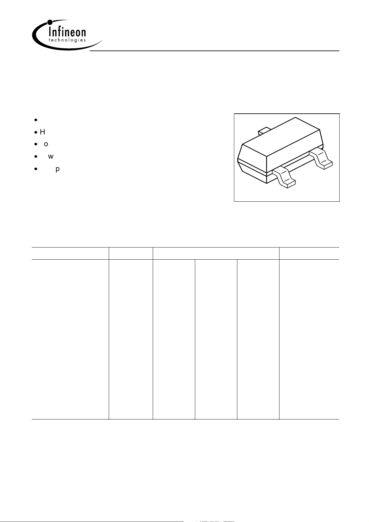
PNP Silicon AF Transistors
For AF input stages and driver applications
High current gain
Low collector-emitter saturation voltage
Low noise between 30 Hz and 15 kHz
Complementary types: BC846, BC847, BC848
BC849, BC850 (NPN)
BC856...BC860
3
1
2
VPS05161
Type Marking Pin Configuration Package
BC856A
BC856B
BC857A
BC857B
BC857C
BC858A
BC858B
BC858C
BC859A
BC859B
BC859C
BC860B
BC860C
3As
3Bs
3Es
3Fs
3Gs
3Js
3Ks
3Ls
4As
4Bs
4Cs
4Fs
4Gs
1 = B
1 = B
1 = B
1 = B
1 = B
1 = B
1 = B
1 = B
1 = B
1 = B
1 = B
1 = B
1 = B
2 = E
2 = E
2 = E
2 = E
2 = E
2 = E
2 = E
2 = E
2 = E
2 = E
2 = E
2 = E
2 = E
3 = C
3 = C
3 = C
3 = C
3 = C
3 = C
3 = C
3 = C
3 = C
3 = C
3 = C
3 = C
3 = C
SOT23
SOT23
SOT23
SOT23
SOT23
SOT23
SOT23
SOT23
SOT23
SOT23
SOT23
SOT23
SOT23
1 Dec-11-2001
Maximum Ratings
g
A
BC856...BC860
Parameter
Symbol
BC856 BC857
BC860
Collector-emitter voltage
Collector-base voltage
Collector-emitter voltage
Emitter-base voltage
DC collector current
Peak collector current
Peak base current
Peak emitter current 200
Total power dissipation, TS = 71 °C P
Junction temperature
Storage temperature
V
V
V
V
I
C
I
CM
I
BM
I
EM
T
T
CEO
CBO
CES
EBO
tot
j
st
65 45 30 V
80 50 30
80 50 30
5 5 5
100 mA
200 mA
200
330 mW
150 °C
-65 ... 150
Thermal Resistance
Junction - soldering point
1)
R
thJS
240 K/W
BC858
BC859
Unit
Electrical Characteristics at T
= 25°C, unless otherwise specified.
Parameter Symbol Values Unit
min. typ. max.
DC Characteristics
Collector-emitter breakdown voltage
= 10 mA, IB = 0
I
C
Collector-base breakdown voltage
I
= 10 µA, IE = 0
C
1
For calculation of R
please refer to Application Note Thermal Resistance
thJA
BC856
BC857/860
BC858/859
BC856
BC857/860
BC858/859
V
(BR)CEO
V
(BR)CBO
65
45
30
80
50
30
-
-
-
-
-
-
V
-
-
-
-
-
-
2 Dec-11-2001
Electrical Characteristics at TA = 25°C, unless otherwise specified.
BC856...BC860
Parameter
DC Characteristics
Collector-emitter breakdown voltage
I
= 10 µA, VBE = 0
C
Emitter-base breakdown voltage
I
= 1 µA, IC = 0
E
Collector cutoff current
V
= 30 V, IE = 0
CB
Collector cutoff current
V
= 30 V, IE = 0 , TA = 150 °C
CB
DC current gain 1)
I
= 10 µA, VCE = 5 V
C
BC856
BC857/860
BC858/859
h
-group A
FE
h
-group B
FE
h
-group C
FE
Symbol Values Unit
min. typ. max.
V
(BR)CES
V
(BR)EBO
I
CBO
I
CBO
h
FE
80
50
30
5 - -
- - 15 nA
- - 5 µA
-
-
-
-
-
-
140
250
480
V
-
-
-
-
-
-
-
DC current gain 1)
I
= 2 mA, VCE = 5 V
C
Collector-emitter saturation voltage1)
I
= 10 mA, IB = 0.5 mA
C
I
= 100 mA, IB = 5 mA
C
Base-emitter saturation voltage 1)
I
= 10 mA, IB = 0.5 mA
C
I
= 100 mA, IB = 5 mA
C
Base-emitter voltage 1)
I
= 2 mA, VCE = 5 V
C
I
= 10 mA, VCE = 5 V
C
h
-group A
FE
h
-group B
FE
-group C
h
FE
h
FE
V
CEsat
V
BEsat
V
BE(ON)
125
220
420
-
-
-
-
600
-
180
290
520
75
250
700
850
650
-
250
475
800
300
650
-
-
750
820
mV
1) Pulse test: t ≤=300µs, D = 2%
3 Dec-11-2001
 Loading...