

Page 1

SERVICE
MANUAL
MF/HF MARINE TRANSCEIVER
|M803
S-15612X Z- C1
March 2020
Page 2

INTRODUCTION
SERVICE CAUTION
This service manual describes the latest technical
information for the IC-M803 MF/HF MARINE
TRANSCEIVER at the time of publication.
MODEL VERSION
IC-M803 USA #11
To upgrade quality, any electrical or mechanical parts and
internal circuits are subject to change without notice or
obligation.
MICROPHONE
HM -214
VERSION
NUMBER
NEVER connect the transceiver to an AC outlet or
to a DC power supply that outputs more than the
specified voltage. This will ruin the transceiver.
DO NOT expose the transceiver’s main unit to rain,
snow or liquids.
DO NOT reverse the polarity of the DC power cable
when directly connecting to the transceiver.
DO NOT apply an RF signal of more than 20 dBm
(100 mW) to the antenna connector. This could
damage the transceiver’s front-end.
REMOTE CONTROLLER
IC-M803
ORDERING PARTS
Be sure to include the following four points when
ordering replacement parts:
1. 10-digit Icom part number
2. Component name
3. Equipment model name and unit name
4. Quantity required
<ORDER EXAMPLE>
1130016460 R2A 20169SA IC-M803 MAIN UNIT 5 pieces
8930102460 4100 IC CLIP IC-M803 CHASSIS 1 piece
Addresses are provided on the inside back cover for
your convenience.
MAIN UNIT
IC-M803
REPAIR NOTES
1. Make sure that the problem is internal before
disassembling the transceiver.
2. DO NOT open the transceiver until it is
disconnected from its power source.
3. DO NOT short any circuits or electronic parts.
4. DO NOT keep power ON for a long time when the
transceiver is defective.
5. NEVER directly transmit power into any test
equipment such as Standard Signal Generator,
otherwise the RF power may damage them.
6. ALWAYS connect a 50 dB to 60 dB attenuator
between the transceiver and such test equipment.
7. READ the instructions of the test equipment
thoroughly before connecting it to the transceiver.
8. If the front panel and case of the remote controller
are separated and reassembled, waterproof
performance will not be guaranteed unless the
specified waterproof check is performed.
Icom, Icom Inc. and the Icom logo are registered trademarks of Icom Incorporated (Japan) in Japan, the United States, the
United Kingdom, Germany, France, Spain, Russia, Australia, New Zealand, and/or other countries.
Page 3

TABLE OF CONTENTS
SECTION 1 SPECIFICATIONS
SECTION 2 INSIDE VIEWS
SECTION 3 DISASSEMBLY INSTRUCTION
SECTION 4 INTERFACE INFORMATION
SECTION 5 ADJUSTMENT PROCEDURE
5-1 PREPA R ATION ……………………………………………………………………………………… 5-1
5-2 FREQUENCY ADJUSTMENT ……………………………………………………………………… 5-3
5-3 RECEIVE ADJUSTMENTS ………………………………………………………………………… 5-3
5-4 TRANSMIT ADJUSTMENTS ……………………………………………………………………… 5-4
5-5 BACKUP BATTERY FLOWING CURRENT VERIFICATION …………………………………… 5-6
5-6 DSC SELF CHECK TEST…………………………………………………………………………… 5-6
SECTION 6 PARTS LIST
SECTION 7 MECHANICAL PARTS
SECTION 8 BOARD L AYO UTS 5
SECTION 9 WIRING DIAGRAM
SECTION 10 BLOCK DIAGRAM
SECTI ON 11 VOLTAGE DIAGRAM1
Page 4

SECTION 1 SPECIFICATIONS
■ GENERAL
• Frequency coverage:
Transceiver RX 0.5 ~ 29.9999 MHz (Continuously)
TX 1.6
4.0
6.0
8.0
12.0
16.0
18.0
22.0
25.0
DSC receiver 2.1875 MHz, 4.2075 MHz, 6.3120 MHz, 8.4145 MHz, 12.5770 MHz,
16.8045 MHz
• Operating mode:
Transceiver J3E (USB/LSB), J2B (AFSK), F1B (FSK), A1A (CW), and H3E (AM: RX only)
DSC receiver J2B
• Antenna impedance: 50 Ω (unbalanced)
• Frequency stability:
Transceiver ±10 Hz (29.9999 MHz or less)
DSC receiver ±10 Hz
• Power supply voltage: 13.6 V DC ±15% (negative ground)
• Current drain:
RX (at maximum audio) Less than 3.0 A
TX (at maximum power) Less than 30 A
• Operating temperature range: −20ºC~ +55ºC (−4ºF~+131º F)
• Dimensions (projections not included):
Transceiver’s main unit 240 (W) × 94 (H) × 238 (D) mm, 9.4 (W) × 3.7 (H) × 9.4 (D) inches
Remote controller 274 (W) × 114 (H) × 86 (D) mm, 10.8 (W) × 4.5 (H) × 3.4 (D) inches
• Weight (approximate):
Transceiver’s main unit 4.41 kg, 9.7 Ib
Remote controller 760 g, 1.7 Ib
2.9999 MHz
~
4.9999 MHz
~
6.9999 MHz
~
8.9999 MHz
~
13.9999 MHz
~
17.9999 MHz
~
19.9999 MHz
~
22.9999 MHz
~
27.5000 MHz
~
■ TRANSMITTER
• Output power: 150/100/60/20 W PEP (1.6~27.5000 MHz)
• Spurious emission: Less than −62 dB (peak output power)
• Carrier suppression: More than 40 dB (peak output power)
• Unwanted sideband suppression: More than 55 dB (peak output power with 1500 Hz AF input)
■ RECEIVER
• Sensitivity:
Transceiver
J3E, A1A 0.5~1.5999 MHz 30 dBμV emf (20 dB SINAD) / 16 dBμV (10 dB S/N)
1.6~1.7999 MHz 13 dBμV emf (20 dB SINAD) / ‒1 dBμV (10 dB S/N)
1.8~29.9999 MHz 8 dBμV emf (20 dB SINAD) / ‒6 dBμV(10 dB S/N)
J2B, F1B 1.6~1.7999 MHz 4 dBμV emf (20 dB SINAD) / ‒10 dBμV (10 dB S/N)
1.8~29.9999 MHz −1 dBμV emf (20 dB SINAD) / ‒15 dBμV (10 dB S/N)
H3E 0.5~1.5999 MHz 44 dBμV emf (20 dB SINAD) / 30 dBμV(10 dB S/N)
1.6~1.7999 MHz 30 dBμV emf (20 dB SINAD) / 16 dBμV (10 dB S/N)
1.8~3.9999 MHz 24 dBμV emf (20 dB SINAD) / 10 dBμV (10 dB S/N)
DSC receiver 6 dBμV emf (20 dB SINAD) / ‒8 dBμV(10 dB S/N)
−6 dBμV emf (1% BER)
• Squelch Sensitivity:
J3E (at 12.230 MHz) Less than +20 dBμV (threshold)
Less than +90 dBµV (tight)
H3E (at 1.000 MHz) Less than +30 dBμV (threshold)
Less than +110 dBµV (tight)
• Spurious rejection ratio:
Transceiver More than 70 dB (0.5~29.9999 MHz)
DSC receiver More than 70 dB
• Clarity variable range: ±150 Hz
All stated specifications are subject to change without notice or obligation.
1-1
Page 5

SECTION 2 INSIDE VIEWS
• LOGIC UNIT (Remote Controller)
RAM
(IC9121)
J9051
J9052
FRONT CPU
(IC9001)
J9151
J9401
9.8304 MHz
CRYSTAL OSCILLATOR
(X9091)
CLONING DATA INTERFACE
(IC9402)
RESET IC
(IC9091)
J9201
8 V REGULATOR
(IC9252)
J9402
MIC AMPLIFIER
(IC9301)
J9091
3.3 V REGULATOR
(IC9254)
J9092
2-1
Page 6

• MAIN UNIT
SOURCE DRIVER
METER AMPLIFIER
SOURCE DRIVER
POWER SUPPLY CIRCUIT
(Under the shield cover)
24.576 MHz FPGA CLOCK
AF POWER AMPLIFIER
BUFFER
PRE-AMPLIFIER CIRCUIT
ALC AMPLIFIER
(IC5911)
J5101
(IC5921)
(Under the shield cover)
J4941
J5102
FLASH ROM
(IC5104)
REAL TIME CLOCK IC
(IC5081)
REALTIME CLOCK
BACKUP BATTERY
(BT5081)
J5071
[MAINTENANCE]
CPU
(IC4901)
EEPROM
(IC5001)
(IC4072)
J4071
D/A CONVERTER
HIGH-VOLTAGE
HIGH-VOLTAGE
A/D CONVERTER
D/A CONVERTER
EXPANDER
(IC5063)
PRE-AMPLIFIER CIRCUIT
(for DSC receiver)
EXPANDER
(IC5064)
EXPANDER
(IC5062)
BPFs
(for DSC receiver)
(IC5051)
(IC4001)
(IC4002)
(IC5201)
(IC5281)
EXPANDER
(IC5061)
J4001
J4141
[ACC]
FPGA
(IC5101)
EEPROM
(IC5001)
OSCILLATOR CIRCUIT
AF LPF
(IC5541)
–12 V DC-DC
CONVERTER
D/A CONVERTER
(IC5501)
J4201
J4051
A/D CONVERTER
(IC5621)
AF LPF
(IC5521)
(for transceiver)
J4181
J4161
[EXT-SP]
BPFs
(for transceiver)
J4701
YGR AMPLIFIER CIRCUIT
J4401
2-2
J4421
(IC5601)
Page 7

• PA UNIT
POWER SUPPLY
LINE SWITCH
(Q6702)
J6703
5 A FUSE
(F2)
BUFFER
(Q6101)
DRIVE AMPLIFIER
CURRENT SENSOR
POWER AMPLIFIER
(Q6202)
(IC6503)
(Q6302)
J6101
BUFFER
(IC6101)
BUFFER
(IC6201)
DRIVE AMPLIFIER
(Q6201)
J6701
COOLING FAN DRIVER
(Q6501)
BUFFER
(IC6401)
BUFFER
(IC6402)
POWER AMPLIFIER
(Q6303)
POWER AMPLIFIER
(Q6301)
J6501
POWER AMPLIFIER
(Q6304)
J6401
CURRENT SENSOR
(IC6502)
2-3
Page 8
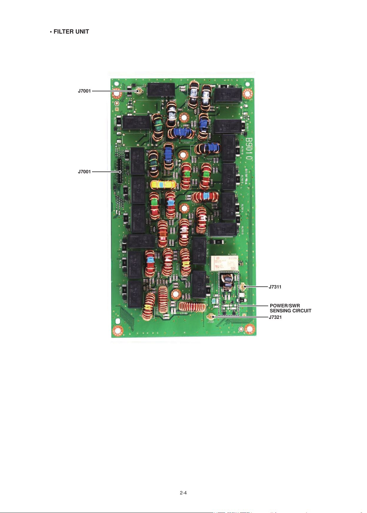
• FILTER UNIT
J7001
J7001
J7311
POWER/SWR
SENSING CIRCUIT
J7321
2-4
Page 9

• CONNECT UNIT
J7751
[GPS-DATA]
RS-232 INTERFACE
(IC7721)
J7721
[REMOTE]
NMEA1 INTERFACE
(IC7751)
NMEA1 INTERFACE
(IC7791)
RS-232 INTERFACE
(IC7723)
NMEA1 INTERFACE
(IC7741)
J7761
RS-232 INTERFACE
(IC7722)
NMEA1 INTERFACE
(IC7731)
J7711
[AF/MOD]
GPS MODULE
(IC7701)
W3010 (CHASSIS)
[GPS-ANT]
+3.3 V REGULATOR
(IC7703)
J7701
3.3 V REGULATOR
(IC7702)
2-5
Page 10
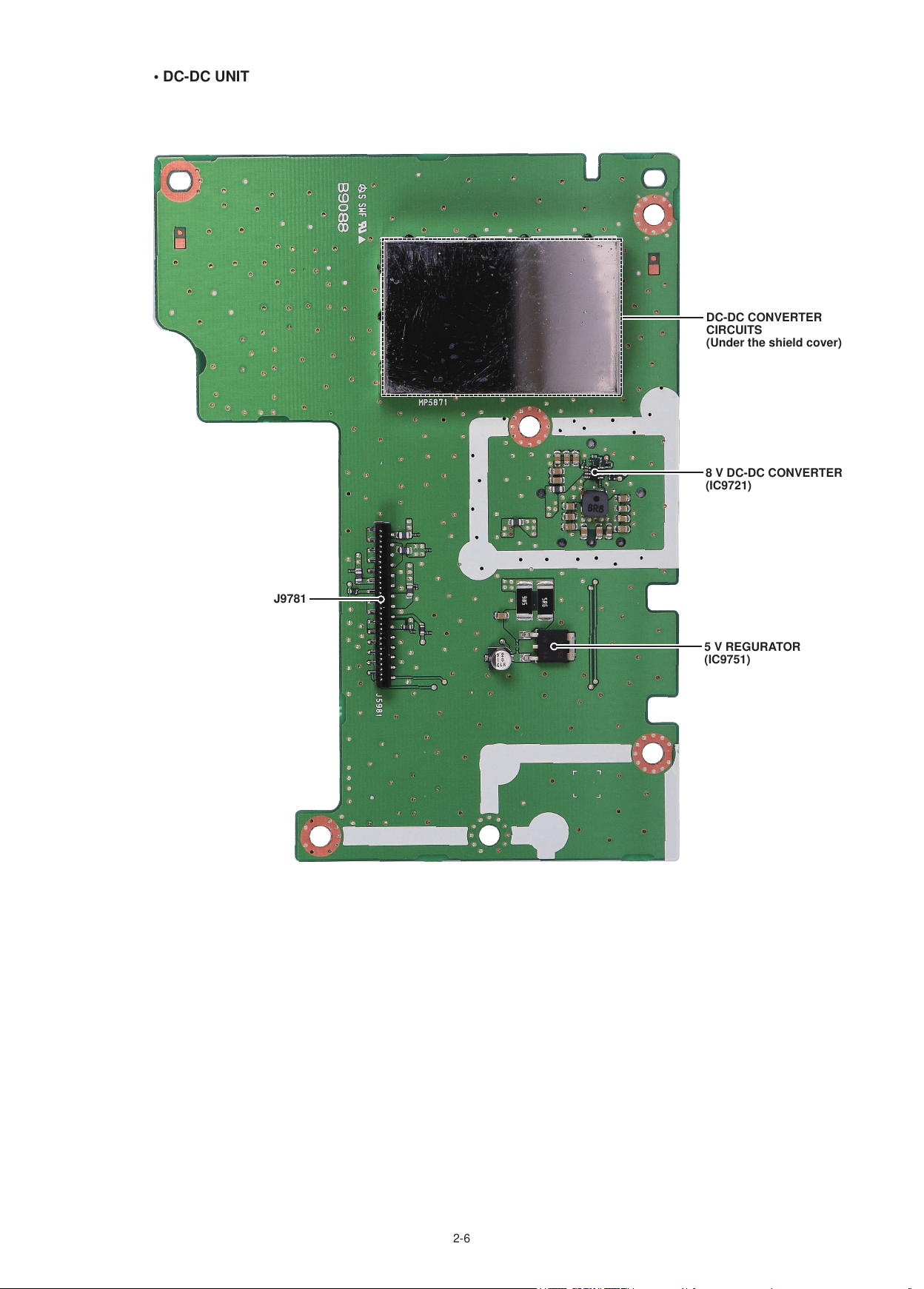
• DC-DC UNIT
DC-DC CONVERTER
CIRCUITS
(Under the shield cover)
8 V DC-DC CONVERTER
(IC9721)
J9781
5 V REGURATOR
(IC9751)
2-6
Page 11

SECTION 3 DISASSEMBLY INSTRUCTION
1. REMOVING THE PA UNIT
1) Remove the 8 screws from the top cover, and then
remove the top cover from the chassis.
Top cover
Screws × 8
3) Remove the 8 screws from the PA cover, and then
separate the PA cover from the chassis as shown in the
illustration below.
Disconnect the cooling fan cable from the PA UNIT, and
then remove the PA cover from the chassis.
Screws × 8
PA cover
Cooling fan cable
Chassis
2) Remove the coaxial cable from the 2 cable hooks on the
PA cover.
PA cover
Coaxial cable
Chassis
J6501J6501
PA UNIT
4) Disconnect the tuner cable, flat cable, and 2 coaxial
cables from the PA UNIT.
PA UNIT
Coaxial cable
J6401
J6401
Flat cable
J6701
J6701
Coaxial cable
J6703J6703
J6101
J6101
Tuner cable
Cable hooks
Continued on the next page…
3-1
Page 12

1. REMOVING THE PA UNIT (continued)
5) Remove the 11 screws from the 3 FETs and the 4 FET
covers on the PA UNIT.
Screws × 11
2. REMOVING THE MAIN UNIT
1) Remove the IC clip from the MAIN UNIT.
Disconnect the control cable, 2 coaxial cables, and 3 flat
cables from the MAIN UNIT.
FET covers
PA UNIT
FETs
6) Remove the 2 screws from the DC power cables to
disconnect the cables from the PA unit.
Screws × 2
DC power cables
PA UNIT
IC clip
Control cable
Flat cables
MAIN UNIT
J4201
J4201
J4051
J4051
J4181J4181
J4421
J4421
J4001
J4001
J4701
J4701
Coaxial cables
Flat cable
2) Remove the 9 screws from the MAIN UNIT, and then
remove the MAIN UNIT from the chassis.
Screws × 9
7) Remove the 4 screws from the PA UNIT, and then
remove the PA UNIT from the chassis.
PA UNIT
Screws × 4
Chassis
MAIN UNIT
Chassis
3-2
Page 13
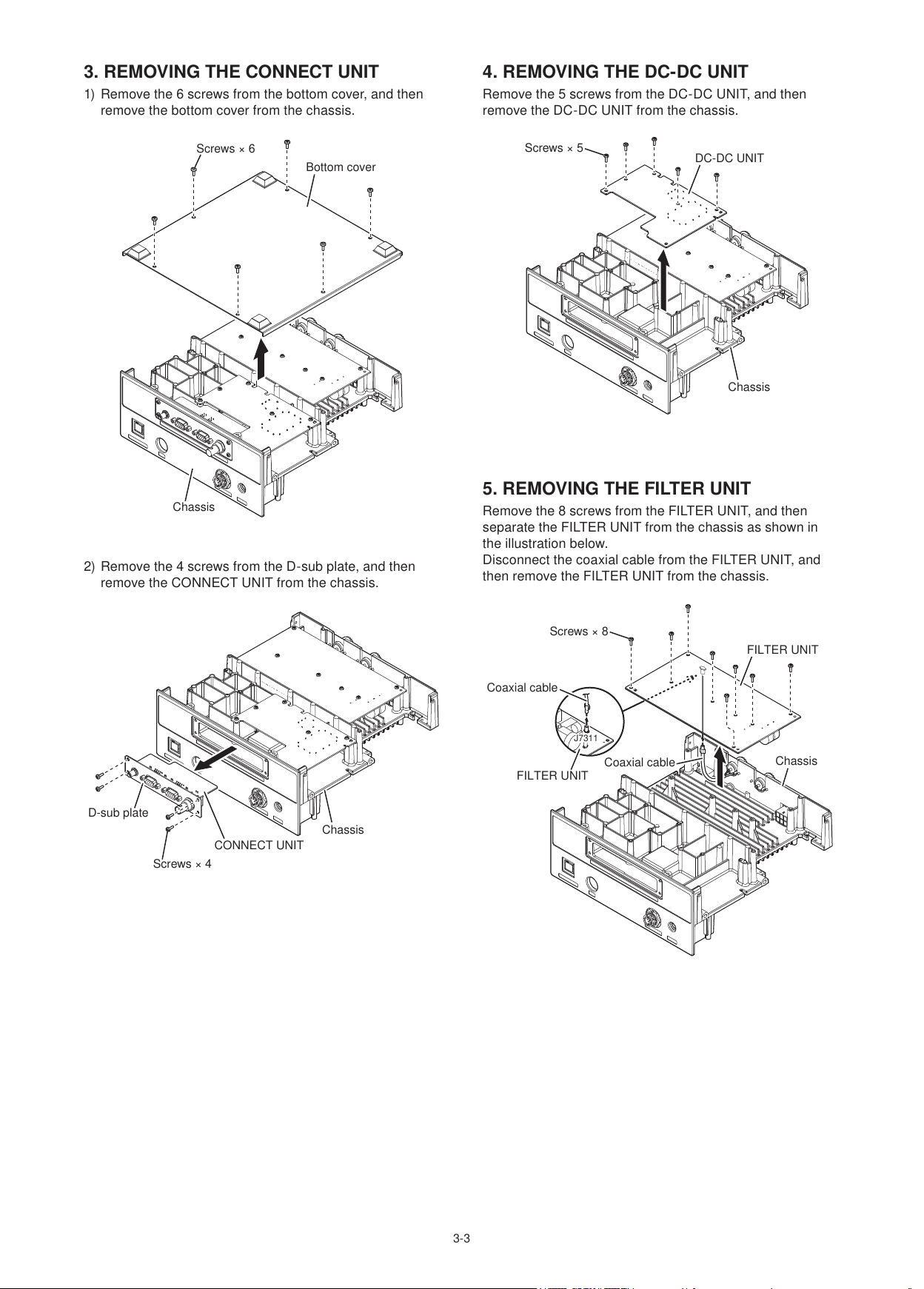
3. REMOVING THE CONNECT UNIT
1) Remove the 6 screws from the bottom cover, and then
remove the bottom cover from the chassis.
4. REMOVING THE DC-DC UNIT
Remove the 5 screws from the DC-DC UNIT, and then
remove the DC-DC UNIT from the chassis.
Screws × 6
Bottom cover
Chassis
2) Remove the 4 screws from the D-sub plate, and then
remove the CONNECT UNIT from the chassis.
Screws × 5
DC-DC UNIT
Chassis
5. REMOVING THE FILTER UNIT
Remove the 8 screws from the FILTER UNIT, and then
separate the FILTER UNIT from the chassis as shown in
the illustration below.
Disconnect the coaxial cable from the FILTER UNIT, and
then remove the FILTER UNIT from the chassis.
D-sub plate
Screws × 4
CONNECT UNIT
Chassis
Coaxial cable
FILTER UNIT
Screws × 8
J7311J7311
Coaxial cable
FILTER UNIT
Chassis
3-3
Page 14
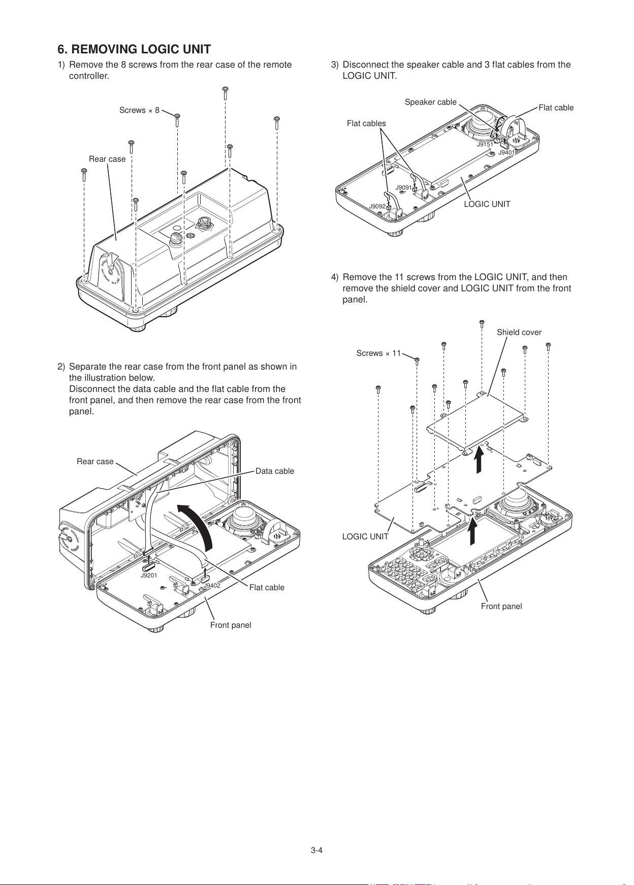
6. REMOVING LOGIC UNIT
1) Remove the 8 screws from the rear case of the remote
controller.
3) Disconnect the speaker cable and 3 flat cables from the
LO GIC UN IT.
Screws × 8
Rear case
2) Separate the rear case from the front panel as shown in
the illustration below.
Disconnect the data cable and the flat cable from the
front panel, and then remove the rear case from the front
panel.
Speaker cable
Flat cable
Flat cables
J9151
J9151
J9401J9401
J9091J9091
J9092
J9092
LOGIC UNIT
4) Remove the 11 screws from the LOGIC UNIT, and then
remove the shield cover and LOGIC UNIT from the front
panel.
Shield cover
Screws × 11
Rear case
J9201
J9201
J9402J9402
Front panel
Data cable
LOGIC UNIT
Flat cable
Front panel
3-4
Page 15

SECTION 4 INTERFACE INFORMATION
• REMOTE CONTROLLER
[MIC]
[MIC]
MIC
Pin
number
Pin
name
1 MIC+ Audio input from the microphone element. Input impedance: 1.74 kΩ ±20%
2 NC No connection. –
3 AF1
4 AF2
Audio output related to the volume setting.
Connected to pin 4 in the microphone.
Audio input.
Connected to pin 3 in the microphone.
5 PTT PTT switch input. When grounded, transmits.
2
8-pin
1
3
7
6
8
5
4
6 GND Ground terminal for transceiver. –
Front panel view
7 MIC‒ Ground terminal for MIC+. –
8 AF‒ Ground terminal for AF1 and AF2. –
• TRANSCEIVER FRONT PANEL (1)
EXT-SP
[ACC]
CONTROLLER
Description Specification
–
–
ACC MAINTENANCE
[ACC]
ACC
8-pin
67
8
3
Front panel view
1
45
2
Pin
number
1 CWK CW and FSK keying input.
Pin
name
Description Specification
Input level: −0.5~+0.8 V
2 AF GND Ground terminal for AF. –
3 SEND
4 MOD
5 AF
Input/Output terminal.
Transmits when grounded.
Modulator input.
- Usable when pin 3 is grounded.
Audio detector output.
- Fixed, regardless of [VOL] position.
Ground level: −0.5~+0.8 V
Input current: Less than 20 mA
Input impedance: More than 10 kΩ
Input level: Approximately
Output impedance:
Output level: 100~300 mV rms
6 NC No connection. –
7 13.6 V 13.6 V output when power is ON.
8 ALC ALC voltage input.
4-1
Output current: Less than 1 A
Control voltage: −3~0 V
Input impedance: More than 10 kΩ
100 mV rms
Less than 4.7 kΩ
Page 16

• TRANSCEIVER FRONT PANEL (2)
EXT-SP
[AF/MOD]
[REMOTE]
[GPS-DATA]
[AF/MOD]
CONTROLLER
ACC MAINTENANCE
AF/MOD
9-pin
5 1
69
Front panel view
[REMOTE]
REMOTE
9-pin
5 1
Front panel view
69
Pin
number
1 MOD+
Pin
name
Description Specification
Modulation input from an external terminal
unit.
Input impedance: More than 600 Ω
Input level: Approximately
2 MOD− Ground terminal for MOD+. –
3 GND Ground terminal for transceiver. –
Output impedance
Output level: Approximately
4 AF+
Detected audio output for an external
terminal unit.
5 AF− Ground terminal for AF+. –
6 GND Ground terminal for transceiver. –
7 NC This pin is not connected anywhere. –
8 SEND Transmits when grounded.
Ground level: −0.5~+0.8 V
Input current: Less than 20 mA
9 GND Ground terminal for transceiver. –
Pin
number
Pin name Description
1 DCD Carrier detection input.
2
3
RXD Receive data input.
NMEA-OUT NMEA0183 ver 4.10 data output.
TXD Transmit data output.
NMEA-IN NMEA0183 ver 4.10 data input.
4 DTR Terminal ready signal output.
5 GND Ground terminal for transceiver.
6 DSR Data-set-ready signal input.
7 RTS Request-to-send data output.
8 CTS Clear-to-send data input.
9 NC No connection.
0.77 V rms
: More than 600 Ω
770 mV rms
[G PS -DATA]
GPS-DATA
BNC
1
Front panel view
2
Pin
number
1
2
Pin name Description
NMEA
NMEA
NMEA0183 ver 4.10 data input.
Ground for NMEA .
4-2
Page 17

• TRANSCEIVER REAR PANEL
[DC 13.6 V]
[TUNER]
[TUNER]
TUNER
234
1
Rear panel view
[DC 13.6 V]
DC 13.6 V
1 2 3
4 5 6
Rear panel view
Pin
number
Pin
name
Description Specification
1 KEY Key signal input. While tuning: −0.5~+0.8 V
2 STA RT Start/Through signal output.
3 13.6 V 13.6 V output.
Pulled up 8 V, 0 V (100 msec) as a start
signal.
Maximum current
: 2 A
4 E Ground terminal for above signals. –
Pin
number
1~3
4~6
Pin
name
DC input .
DC input .
Description Specification
Maximum power consumption:
30 A typical.
–
4-3
Page 18

SECTION 5 ADJUSTMENT PROCEDURE
5-1 PREPARATION
REQUIRED EQUIPMENT
EQUIPMENT GRADE AND RANGE EQUIPMENT GRADE AND RANGE
DC power supply #1
DC power supply #2
Output voltage: 13.6 V ±15%
Current capacity: 30 A or more
Output voltage: 3.0 V
Current capacity: 1 mA or more
AC millivoltmeter Measuring range: 10 mV to 10 V
Digital multimeter
Measuring range: 0 .1
μA to 1 mA
RF power meter
(50 Ω terminated)
Audio generator
(AG)
CONNECTIONS
MICROPHONE
HM-214H
AC
millivoltmeter
generator
MIC
[MIC]
Measuring range: 1 ~ 150 W
Frequency range: 0.1 ~ 30 MHz
SWR: Less than 1.2 : 1
Frequency range: 300 ~ 3000 Hz
Output level: 1 ~ 500 mV
IC-M803’s CONTROLLER
[MIC]
Audio
MICE
Remote Control cable
Standard signal
generator (SSG)
Dummy Load
To [MAIN UNIT]
To [CONTROLLER]
Rear panel view
Frequency range: 0.1 ~ 30.000000 MHz
Output level: −20 to 100 dBμ
(−127 to −7 dBm)
Impedance: 100 Ω (VSWR 2:1)
Capacity: More than 150 W
IC-M803’s MAIN UNIT
RF POWER METER
(150 W/50 Ω)
DUMMY LOAD
(100 Ω/150 W)
Used for SWR meter adjustments. (VSWR 2:1)
NEVER TRANSMIT while the SSG is connected.
DC POWER SUPPLY #1
(13.6 V/30 A)
To [DSC ANT] To [DC 13.6 V]To [ANT]
Red
Black
STANDARD SIGNAL GENERATOR
(0.1~30.000000 MHz)
5-1
Page 19

ENTERING THE I/O VERIFICATION MODE
1. Turn OFF the power.
2. While holding down all [DISTRESS], [SOFT KEY 1],
and [►], turn ON the transceiver power to enter the I/O
verification mode.
ENTERING THE ADJUSTMENT MODE
1. Turn OFF the power.
2. While holding down all , , and
214H
, turn ON the transceiver power to enter the
adjustment mode.
[DOWN]
[▼] on the
HM-
[TUNE]
[DISTRESS] [Soft Key 1] [►] [POWER]
REMOTE CONTROLLER AND
MICROPHONE OPERATION
VERIFICATION
1. Enter the I/O verification mode.
2. Push [▲], and verify the LCD screen changes in order of
maximum backlight, minimum backlight, black, red,
green, and blue brightness.
3. Push the corresponding key that is displayed on the
screen (26 items).
4. Turn or push the corresponding dial that is displayed on
the screen (6 items).
5. Push the corresponding microphone key that is
displayed on the screen (5 items).
[RX/TX]
RECEIVE ADJUSTMENT (TRANSCEIVER)
REFERENCE FREQUENCY ADJUSTMENT
TX POWE AND IDLING CURRENT ADJUSTMENTs
RECEIVE ADJUSTMENT (DSC)
[POWER]
ADJUSTMENT MENU
KEY ASSIGNMENTS FOR THE ADJUST MODE
• Push [▲] or [▼] to select an adjustment item.
• Rotate [CH/GRP] to modify the adjustment value.
• Push
to store the adjustment value, and select the
next adjustment item.
• Push [SOFT KEY 3] or [SOFT KEY 2] to select the next or
previous adjustment item.
• Push [SOFT KEY 1] to return to the adjustment menu screen.
[▲][▼]
6. When all verifications are completed, “Complete” is
displayed on the screen.
5-2
[Soft Key 1]
[Soft Key 2]
[Soft Key 3] [ENT]
[CH/GRP]
Page 20

5-2 FREQUENCY ADJUSTMENT
Enter the adjustment mode.
ADJUSTMENT
REFERENCE
FREQUENCY
ADJUSTMENT ITEM
DISPL AY
1 – • Three minutes have passed since
SETTING CONDITION OPERAT ION
the transceiver is turned ON.
- Preparation -
- Adjustment -
*The output level of the standard signal generator (SSG) is measured at the load end (PD).
2 “REF OSC” • Connect the standard signal
generator (SSG) to the [ANT]
connector, and set it to:
Frequency: 10.000000 MHz
Level*: +94 dBµ (−13 dBm)
Modulation: None
• Receiving
5-3 RECEIVE ADJUSTMENTS
ADJUSTMENT
TOTAL GAIN
ADJUSTMENT ITEM
DISPL AY
1 – – Select the “Total Gain RX (REF)”
- Preparation -
- Adjustment -
S-METER
2 “Total Gain RX (REF)” • Connect the SSG to the [ANT]
3 “Total Gain RX (SET)”
1 “8 Dot Level” • Set the SSG as:
- Adjustment -
DSC RECEIVER
1 – – Select the “Total Gain DSC REF”
TOTAL GAIN
- Preparation -
- Adjustment -
*The output level of the standard signal generator (SSG) is measured at the load end (PD).
2 “Total Gain DSC REF” • Connect the SSG to the [DSC ANT]
3 “Total Gain DSC SET”
SETTING CONDITION OPERAT ION
connector, and set it to:
Frequency: 12.354 MHz
Level*: +50 dBµ (−57 dBm)
Modulation: None
• Receiving
• Turn OFF the SSG output.
• Receiving
Level*: +80 dBµ (−27 dBm)
• Turn ON the SSG output.
• Receiving
connector, and set it to:
Frequency: 8.4145 MHz
Level*: +50 dBµ (−57 dBm)
Modulation: None
• Receiving
• Turn OFF the SSG output.
• Receiving
Select the “REF OSC” item.
(Adjustment menu: “REF OSC”)
Push
(Two beeps sound, then
automatically moves to the Receive
adjustment “Total Gain RX (REF).”)
(Adjustment menu: “R X” > “Total
Gain RX (REF)”)
Push
(Two seconds later, two beeps
sound.)
Push
(Ten seconds later, two beeps
sound.)
Push
(One second later, two beeps
sound.)
(Adjustment menu: “DSC-RX” >
“Total Gain DSC REF”)
Push
(Two seconds later, two beeps
sound.)
Push
(Ten seconds later, two beeps
sound and then automatically
returns to the adjustment menu.)
.
item.
.
.
.
item.
.
.
5-35-3
Page 21

5-4 TRANSMIT ADJUSTMENTS
ADJUSTMENT
IDLING
- Preparation -
- Adjustment -
TX OUTPUT
POWER (HF)
- Preparation -
- Adjustment -
ADJUSTMENT ITEM
DISPL AY
1 – – Select the “VDL IDL Set” item.
2 “VDL IDL Set” • Automatically transmits.
3 “Final 1 IDV (12M)”
4 “Drive 1 IDV”
5 “Pre-Driver IDV”
1 “TX Total HF Gain” • Receiving
2 “TX Total HF Gain” • Automatically transmits. Rotate [CH/GRP] to set the output
3 “Power Tune (12M)” Rotate [CH/GRP] to set the output
4 “Power 20W (12M)” Rotate [CH/GRP] to set the output
5 “Power 60W (12M)” Rotate [CH/GRP] to set the output
6 “Power 100W (12M)” Rotate [CH/GRP] to set the output
7 “Power 150W (12M)” Rotate [CH/GRP] to set the output
8 “Power 150W (4M)”
9 “Power 150W (6M)”
10 “Power 150W (8M)”
11 “Power 150W (16M)”
12 “Power 150W (18M)”
13 “Power 150W (22M)”
14 “Power 150W (25M)”
15 “Power 150W (27M)” Rotate [CH/GRP] to set the output
SETTING CONDITION OPERAT ION
(Adjustment menu: “TX/ID” > “ID” >
“VDL IDL Set”)
( Automatically returns to receive
when the beeps sound.)
automatically moves to the Transmit
• Connect the RF power meter to the
[ANT] connector.
• Connect the audio generator with
the AC millivoltmeter to [MIC]
connector, and set it to:
Frequency: 1.5 kHz
Waveform: Sine wave
Level: 40 mV rms
(Two beeps sound.)
(Two seconds later, two beeps
(One second later, two beeps
(Two beeps sound and then
power adjustment “TX Total HF
power to 70 W, then push .
(Two beeps sound.)
power to 10 W, then push
(Two beeps sound.)
power to 20 W, then push
(Two beeps sound.)
power to 70 W, then push
(Two beeps sound.)
power to 100 W, then push
(Two beeps sound.)
power to 140 W, then push
(Two beeps sound.)
power to 130 W, then push
(Two beeps sound, and then
returns to receive.)
Continued on the next page...
Push
Push
sound.)
Push
sound.)
Push
Gain.”)
Push
.
.
.
.
.
.
.
.
.
.
.
5-4
Page 22

5-4 TRANSMIT ADJUSTMENTS (CONTINUED)
ADJUSTMENT
TX OUTPUT
POWER (MF)
- Adjustment -
ALC
- Adjustment -
DRIVE GAIN
- Adjustment -
SWR
- Preparation -
- Adjustment -
Id APC
- Adjustment -
ADJUSTMENT ITEM
DISPL AY
1 “TX Total MF Gain” • Receiving
2 “TX Total MF Gain”
3 “Power Tune (2.1M)” Rotate [CH/GRP] to set the output
4 “Power 20W (2.1M)” Rotate [CH/GRP] to set the output
5 “Power 60W (2.1M)” Rotate [CH/GRP] to set the output
6 “Power 100W (2.1M)” Rotate [CH/GRP] to set the output
7 “Power 150W (2.1M)” Rotate [CH/GRP] to set the output
8 “Power 150W (1.6M)”
1 “ALC” • Automatically transmits.
1 “Drive Min (12M)” • Automatically transmits.
If a 100 Ω dummy load (or a dummy load with VSWR of 2:1) is unavailable, skip this adjustment.
1 “SWR2”
2 “SWR2” • Automatically transmits.
1 “ID-APC Check” • Automatically transmits.
SETTING CONDITION OPERAT ION
Push
• Automatically transmits. Rotate [CH/GRP] to set the output
power to 70 W, then push
(Two beeps sound.)
power to 10 W, then push
(Two beeps sound.)
power to 20 W, then push
(Two beeps sound.)
power to 70 W, then push
(Two beeps sound.)
power to 100 W, then push
(Two beeps sound.)
power to 140 W, then push
(Two beeps sound, and then
automatically moves to the ALC
adjustment “ALC.”)
Push
(Three seconds later, two beeps
sound and then automatically
enters to the Drive gain adjustment
“Drive Min (12M)” mode.)
Push
(Ten seconds later, two beeps
sound and then automatically
moves to the SWR adjustment
“SWR2.”)
• Connect the 100 Ω dummy load to
the [ANT] connector.
Push
(Three seconds later, two beeps
sound and then automatically
moves to the Id APC adjustment
“ID-APC Check.”)
( Automatically returns to receive
when the beeps sound.)
(Two seconds later, two beeps
sound and then automatically
returns to the adjustment menu.)
Push
.
.
.
–
.
.
.
.
.
.
.
.
5-5
Page 23

5-5 BACKUP BATTERY FLOWING CURRENT VERIFICATION
6
J5081
J5071
J4941
C5081
C5013
C5012
C5011
C4920C4918C4917C4916
C4915
R5108
R5089
R5087
R5086
R5085
R5084
R5083
R5081
R5072R5071
R5026
R5021
R5013
R5012
R5011
R4988
R4109R4108
R4107
EP5071
Q5082
Q5081
IC5081
IC5011
FI5071
EP4901
D5081
D5071
D4101
C4919
C4914
C4101
1. Turn OFF the transceiver’s power.
2. Remove the top cover. (Refer to DISASSEMBLY INSTRUCTIONS in SECTION 3.)
3. Remove the backup battery (BT5081) from J5081 on the MAIN UNIT.
4. Apply 3.0 V DC to the point in the illustration shown below, through the digital multimeter.
5. Verify that the current value indicated on the digital multimeter is less than 0.8 μA.
6. Insert the backup battery into J5081 on the MAIN UNIT, and then attach the top cover.
Backup battery
MAIN UNIT
J5081J5081
DIGITAL MULTIMETER
(0.1 μA to 1 mA )
DC POWER SUPPLY #2
(3.0 V/1 mA or more)
5-6 DSC SELF CHECK TEST
The Self Check test sends DSC signals to the receiving AF circuit to compare the sending and receiving signals at the AF level.
1. Open “Self Check Test.”
[ [MENU] > DSC Settings > Self Check Test ]
2. Push
3. When the sending and receiving DSC signals match, “OK” is displayed.
, or to start the Self Check Test.
5-6
Page 24

SECTION 6 PARTS LIST
[MAIN UNIT] [MAIN UNIT]
REF
NO.
IC40 01 1110008540 S.IC 62783G-S18-R T 130.5/111.3
IC 40 02 11100 08 54 0 S. IC 6278 3G -S 18-R T 118. 3/ 111.8
IC4021 111000855 0 S.IC NJM2904C RB1-TE1-#HMZR T 107.6/109.1
IC4022 111000855 0 S.IC NJM2904C RB1-TE1-#HMZR T 107.6/104.3
IC40 51 1130018870 S.IC TC7WH14FKLJ T 99.8/27.2
IC40 61 1110006921 S.IC S- 80845CNMC-B 86T2G T 176.8/102 .7
IC4071 1130018870 S.IC TC7WH14FKL J T 188.1/104.4
IC4072 1110005140 S.IC NJM3403AV-TE1-#Z ZZB T 156.7/101.2
IC4261 6910027620 S.DC TPS54418RTER T 179.4/70.4
IC4262 1130007021 S.IC TC7S 66FU (TE85LF) T 183.1/82.6
IC4321 1180004970 S.REG XC6222D251MR-G T 174.6/87.0
IC43 31 118000474 0 S.REG S -1313D33-M5T1U3 T 180.0/92.6
IC43 41 1180004740 S.REG S-1313D33- M5T1U3 T 174.6/91.9
IC43 61 1180004430 S.REG XC6209F502MR-G T 117.6/18.5
IC4371 1180004800 S.REG XC6222D181MR-G T 184. 2/92.6
IC43 81 6910028150 S.DC AD P5075ACBZ-R7 T 115.9/12.5
IC4401 1110007400 S.IC BGA616 T 4.8/82.1
IC46 61 1110007400 S.IC BGA616 T 73. 5/49.8
IC46 62 1180004430 S.REG XC6209F502MR-G T 105.1/44.6
IC49 01 1140018901 S.IC STM32F429IGT6 T 177.2/45.5
IC49 02 113001805 0 S.IC SN74AHCT367PWR T 151.4/40.2
IC50 01 113001946 0 S.IC GT24C256A-2ZLI-TR T 173.9/25.2
IC5011 1110005771 S.IC S -80942CNMC-G 9CT2G T 191.4/23.0
IC5051 1130016460 S.IC R2A 20169SA T 144. 5/102.0
IC50 61 1130017400 S.IC MC74HC4094ADTR2G T 131.9/100.8
IC50 62 1130017400 S.IC MC74HC4094ADTR2G T 68.7/84.4
IC50 63 1130017400 S.IC MC74HC4094ADTR2G T 79.2 /86.2
IC50 64 1130017400 S.IC MC74HC4094ADTR2G T 72. 5/115.5
IC5081 1130011551 S.IC RX- 4581NB-F T 205.9/45.7
IC5101 1140018370 S.I C 5 CEFA9F23I7N T 144.6/ 77.0
IC5102 6910 024650 S.IC 74LVC2G17GW125 T 202.5/108.4
IC5103 6910 024650 S.IC 74LVC2G17GW125 T 198.2/108.4
IC5104 1130018770 S.I C S25FL127SABMFI100 T 214.9/57.2
IC5161 1180004430 S.REG XC6209F502MR-G T 94.3/103 .2
IC5181 1110009190 S.IC LTC6401IUD-20#TRPBF T 105. 5/80.3
IC5201 1190005200 S.IC AD9645BCPZRL7-80 T 125. 2/85.9
IC5241 1110009190 S.IC LTC6401IUD-20#TRPBF T 105.7/91.8
IC5281 1190004630 S.IC ISL59 61IAZ T 123.7/69.7
IC5401 1130019760 S.IC IPS6404L-SQ- SPN T 145.1/55.3
IC54 41 1130012160 S.IC SN74LVC1GU04DCKR T 117.8/54.4
IC54 51 1130017950 S.IC SN 65LVDS1DBVR T 116.4/58.8
IC54 61 1130014260 S.IC SN74LVC2GU04DCKR T 123.4/58. 5
IC5491 1130012160 S.IC SN74LVC1GU04DCKR T 123.9/54.4
IC5501 1110007930 S.IC PCM1681PWPR T 88.8/32.6
IC5502 1110008890 S.IC NJU7056F3-TE2-#Z ZZH T 56.3/24.5
IC5521 1110006570 S.IC TS4 62CPT T 5 6.9/37.4
IC55 41 11100040 50 S.IC NJM3404AV-TE1-#FMZB T 133.8/6.4
IC5561 111000855 0 S.IC NJM2904C RB1-TE1-#HMZR T 112.6/49.5
IC5581 111000855 0 S.IC NJM2904C RB1-TE1-#HMZR T 105.3/60.6
IC5601 1110009480 IC STA540-HF
IC5621 1190004280 S.IC PCM1802DBR T 73.1/32.5
IC5651 1130009981 S.IC TC7W53FK (TE85LF) T 58.2/18.5
IC5661 1130009981 S.IC TC7 W53FK (TE8 5LF) T 178.5/16.0
IC5681 1130009981 S.IC TC7 W53FK (TE8 5LF) T 58.2/11.8
IC5911 1110005610 S.IC NJ M2058V-TE1-#Z ZZB T 204.6/89.7
IC5921 1110005610 S.IC NJ M2058V-TE1-#Z ZZB T 195 .7/ 89.7
Q4021 1590005220 S.TRA LDTA114YET1G T 123.1/100.3
Q4022 159 00046 90 S.TRA LDTC143ZET1G T 125.6/100.3
Q4023 159 00046 90 S.TRA LDTC143ZET1G T 125.6/9 8.2
Q4061 153 0004140 S.TRA L2SC4081RT1G T 179.9/103.0
Q4062 159 0005220 S.TRA LDTA114YET1G T 176.9/110.9
Q4063 1550000241 S.FET TPCF8107LF T 177.9/107.4
Q4071 1590004690 S.TR A LDTC143ZET1G T 183.9 /104.9
Q4072 1590005220 S.TRA LDTA114YET1G T 183.9/107.5
Q4073 1530004140 S.TRA L2SC40 81RT1G T 165.2/101.7
Q4141 1530004140 S.TRA L2SC40 81RT1G T 143.5 /10.2
Q4142 1530004140 S.TRA L2SC40 81RT1G T 175.2/11.4
Q4161 1590005220 S.TRA LDTA114YET1G T 146.3/10.1
Q4162 1530004620 S.TRA 2SCR553P5T100 T 146. 5/6.6
Q4341 1560 002210 S.FET RE1J00 2YNTCL T 170.4/81.9
Q4342 159 0005220 S.TRA LDTA114YET1G T 175.0/9 4.8
Q4401 1590005220 S.TRA LDTA114YET1G T 19.2/54.7
Q440 2 159 00046 90 S.TRA LDTC143ZET1G T 19.2/52.2
Q4421 1530003091 S.TR A 2SC4213- B (TE85RF) T 10.4/57.0
Q4422 159 0005220 S.TRA LDTA114YET1G T 17.1/54.7
Q4423 1590004690 S.TR A LDTC143ZET1G T 15.0/54.7
Q4424 1590004690 S.TR A LDTC143ZET1G T 15.0/52.2
Q4426 1590004690 S.TR A LDTC143ZET1G T 21.3 /52.2
Q4427 1590005220 S.TRA LDTA114YET1G T 21.3/54.7
Q4631 1590005220 S.TRA LDTA114YET1G T 106.1/51.5
Q4632 159 00046 90 S.TRA LDTC143ZET1G T 106.1/48.9
Q4641 1530004 560 S.TRA 2SC3356G-B-AE2-R T 73.5/68.2
Q4642 159 0005220 S.TRA LDTA114YET1G T 100.9/54.5
Q4643 159 0005220 S.TRA LDTA114YET1G T 106.1/5 4.5
Q4644 159 00046 90 S.TRA LDTC143ZET1G T 104.1/54.5
Q4661 1590005220 S.TRA LDTA114YET1G T 104.1/51.5
Q466 2 159 0005220 S.TRA LDTA114YET1G T 100.8/51.5
Q466 3 159 00046 90 S.TRA LDTC143ZET1G T 104.1/48 .9
Q4701 1590004690 S.TR A LDTC143ZET1G T 12.7/99.0
Q4702 1530004140 S.TRA L2SC40 81RT1G T 13.9/96.3
Q4871 1590005220 S.TRA LDTA114YET1G T 113.3/97.8
Q4872 1590004690 S.TR A LDTC143ZET1G T 116.9/97.8
Q4881 1530004560 S.TR A 2SC3356 G-B- AE2-R T 8 0.5/109.0
Q4882 159 0005220 S.TRA LDTA114YET1G T 113.3/93.3
Q488 3 159 0005220 S.TRA LDTA114YET1G T 113.3/95.3
Q488 4 159 00046 90 S.TRA LDTC143ZET1G T 116.9/95.3
Eqv.= This component is equivalent to the REF No. component listed above,
PART
NO.
DESCRIPTION M.
and may be substituted on parts orders and repairs.
H/V
LOCATION
REF
NO.
Q5041 1590004690 S.TR A LDTC143ZET1G T 158 .5/50.4
Q5042 1530004140 S.TRA L2SC40 81RT1G T 155.8/51.1
Q5081 15100005 02 S.TRA 2SA1162-GRLF T 212.0/44.5
Q5082 153 0004140 S.TRA L2SC4081RT1G T 211.9/41.5
Q5421 153000459 0 S.TRA BFR193F H6327 T 118.8/48.2
Q5422 1510001270 S.TRA 2SAR502UBTL T 120.1/50.7
Q5481 153000459 0 S.TRA BFR193F H6327 T 124.7/48.2
Q5482 1510001270 S.TRA 2SA R502UBTL T 126.0/50.7
Q5581 1530004140 S.TRA L2SC40 81RT1G T 99.3/58.5
Q5582 153 0004140 S.TRA L2SC4081RT1G T 109.7/57.2
Q5651 1590004690 S.TR A LDTC143ZET1G T 5 4.5/18.8
Q5661 1590004690 S.TR A LDTC143ZET1G T 181.5/18.7
Q5681 1590004690 S.TR A LDTC143ZET1G T 54.5/12.1
Q5901 1590005220 S.TRA LDTA114YET1G T 209.4/81.0
Q5902 1550000610 S. FET RU1L002SNTL T 209.6/78.7
Q5911 1530004140 S.TRA L2SC40 81RT1G T 209.5/83.4
Q5931 1590005220 S.TRA LDTA114YET1G T 199.2/82.8
Q5932 1590004690 S.TR A LDTC143ZET1G T 199.6/76.8
Q5981 1510001270 S.TRA 2SAR502UBTL T 203.5/79.6
D4021 1750001810 S.DIO L1SS 400T1G T 109.7/101.4
D4023 1750001820 S.DIO LRB706F-40T1G T 119.8/100.1
D4024 1750001820 S.DIO LRB706F-40T1G T 119.8/102.6
D4035 1750001810 S.DIO L1SS400T1G T 103.5/102.1
D4071 1750001820 S.DIO LRB706F-40T1G T 187.1/107.2
D4072 1750001820 S.DIO LRB706F-40T1G T 185.5/100.9
D4074 1750001820 S.DIO LRB706F-40T1G T 137.7/104.8
D4101 1750001820 S.DIO LRB706F-40T1G T 191.7/15.6
D4102 1750001820 S.DIO LRB706F-40T1G T 173.7/100.3
D4103 1750001820 S.DIO LRB706F-40T1G T 171.2/100.3
D4141 1750001810 S.DIO L1SS 400T1G T 146.9/13.0
D4142 1750001810 S.DIO L1SS 400T1G T 171.6/9.2
D438 3 1750002110 S.DIO LRB551V-30T1G T 114.5/4.5
D4401 179 0001622 S.D IO 1SV308L3F T 8.7/82.7
D4421 179 0001622 S.D IO 1SV308L3F T 10.4/ 69.0
D443 4 1750003040 S.DIO L709CEAR T 5.4/5 9.9
D443 5 1750003040 S.DIO L709CEAR T 5.4 /57. 2
D4451 179 0001622 S.D IO 1SV308L3F T 17.4/ 79.9
D4452 1790001622 S.DIO 1SV308L3F T 17.4/64.1
D4471 179 0001622 S.D IO 1SV308L3F T 22.0 /85.6
D4472 179 0001622 S.D IO 1SV308L3F T 22 .0/64.1
D4491 179 0001622 S.D IO 1SV308L3F T 26.6/85.6
D4492 1790001622 S.DIO 1SV308L3F T 26.7/64.1
D4511 179 0001622 S.D IO 1SV308L3F T 32.7/85.6
D4512 179 0001622 S.D IO 1SV308L3F T 32.7/64.1
D4531 179 0001622 S.D IO 1SV308L3F T 38.8 /85.6
D4532 1790001622 S.DIO 1SV308L3F T 38.8/64.1
D4551 179 0001622 S.D IO 1SV308L3F T 44.9 /85.6
D4552 1790001622 S.DIO 1SV308L3F T 4 4.9/64.1
D4571 179 0001622 S.D IO 1SV308L3F T 49.4/85.6
D4572 179 0001622 S.D IO 1SV308L3F T 49.4/64.1
D4591 179 0001622 S.D IO 1SV308L3F T 53.9 /85.6
D4592 1790001622 S.DIO 1SV308L3F T 54.0/63.2
D4611 179 0001622 S.D IO 1SV308L3F T 59.2 /85.6
D4612 179 0001622 S.D IO 1SV308L3F T 59.3/63.2
D4631 179 0001622 S.D IO 1SV308L3F T 69.6/60.0
D4632 1790001622 S.DIO 1SV308L3F T 84.9/57.8
D4641 17900 01622 S.DIO 1SV30 8L3F T 69.6/6 5.1
D4642 1790001622 S.DIO 1SV308L3F T 8 4.9/68.1
D4643 1750001810 S.DIO L1SS400T1G T 102.5/54.6
D4661 179 0001622 S.D IO 1SV308L3F T 6 8.1/60.0
D4662 1750003070 S.DIO BAP70Q T 69.2/54.2
D466 3 1750003070 S.DIO BAP70Q T 78.2/52.6
D466 4 1750003070 S.DIO BAP70Q T 87.9/52.6
D466 5 1750001810 S.DIO L1SS400T1G T 102. 5/51.4
D466 6 1790001622 S.DIO 1SV308L3F T 92.0/52.2
D4701 1750003040 S.DIO L709CEAR T 10.9/106. 8
D4702 1750003040 S.DIO L709CEAR T 13.6/106.8
D4703 1750001820 S.DIO LRB706F-40T1G T 16.6/108.5
D4704 1750001810 S.DIO L1SS 400T1G T 12.3/101.6
D4731 179 0001622 S.D IO 1SV308L3F T 18.5/91.7
D4732 179 0001622 S.D IO 1SV308L3F T 20.4/115.4
D4751 179 0001622 S.D IO 1SV308L3F T 25.9/91.7
D4752 179 0001622 S.D IO 1SV308L3F T 26.5/114.8
D4771 179 0001622 S.D IO 1SV308L3F T 33.5/91.7
D4772 179 0001622 S.D IO 1SV308L3F T 33.6/113.5
D4791 179 0001622 S.D IO 1SV308L3F T 41.0/91.7
D4792 179 0001622 S.D IO 1SV308L3F T 41.0/115.9
D4811 179 0001622 S.D IO 1SV308L3F T 49.2 /90.5
D4812 179 0001622 S.D IO 1SV308L3F T 49. 2/115.2
D4841 17900 01622 S.DIO 1SV30 8L3F T 57.0/90.5
D4842 1790001622 S.DIO 1SV308L3F T 56.8/115.2
D4871 179 0001622 S.D IO 1SV308L3F T 71.6/110.2
D4872 179 0001622 S.D IO 1SV308L3F T 71.6/97.6
D4881 179 0001622 S.D IO 1SV308L3F T 77.0/110.2
D4882 1750001810 S.DIO L1SS400T1G T 115.9/92.8
D488 3 1790001622 S.DIO 1SV308L3F T 81.5/97.6
D5071 1750003410 S.ZEN RCLAMP7524T.TNT T 197.7/14.8
D5081 1750001810 S.DIO L1SS 400T1G T 215.8/42.8
D5161 1750003070 S.D IO BAP70Q T 88.1/71.7
D5221 1750003070 S.D IO BAP70Q T 90.1/99.1
D5901 1750001810 S.DIO L1SS 400T1G T 205.6/79. 4
D5921 1750001810 S.DIO L1SS 400T1G T 193.7/80.5
D5941 1750001810 S.DIO L1SS 400T1G T 200.7/96.8
D5951 1750001810 S.DIO L1SS 400T1G T 209.4/97.9
D5961 1750001810 S.DIO L1SS 400T1G T 191.0/96.8
D5962 1750001810 S.DIO L1SS400T1G T 192.2/ 96.8
PART
NO.
M.= Mounted side (T: Mounted on the Top side, B: Mounted on the Bottom side)
H/V LOCATION=See the BOARD LAYOUTS for details.
6-1
DESCRIPTION M.
H/V
LOCATION
Page 25

[MAIN UNIT] [MAIN UNIT]
REF
NO.
D5963 1750001810 S.DIO L1SS400T1G T 195.7/97.2
D5971 1750001810 S.DIO L1SS 400T1G T 199.3/98.7
FI5071 4580000260 S.FIL EXC24C F900U T 199.4/14.6
X4921 6050014950 S. XTA CR-1084 (9.8304 MHz) T 159.8 /40.6
X5421 6050014940 S. XTA CR-1083 (73.728 MHz) T 118.7/43.7
X5481 6 050014930 S. XTA CR-1082 (24.576 MHz) T 124.3/42.7
L4071 6200017540 S.COI NLV25T-101J-EF T 171.5 /116. 2
L4072 6200017540 S.COI NLV25T-101J-EF T 14 8.8/110.0
L4075 6200017540 S.COI NLV25T-101J-EF T 138.0/110.0
L4076 6200017540 S.COI NLV25T-101J-EF T 152.6/110.0
L4141 6200017540 S.COI NLV25T-101J-EF T 148.1/16.0
L4144 6200017540 S.COI NLV25T-101J-EF T 171.5/11.6
L4182 6200017700 S.COI NLV32T-221J-EF T 33.0/36.8
L4183 620001770 0 S.COI NLV32T-221J- EF T 36.0/36.8
L4261 6200 016430 S.COI VLS5 045EX-3 R3N T 172.8/70.6
L4282 620 0015100 S.COI MLP2520S100MT T 10 4.3/15.5
L4381 6200 016400 S.COI VLS5045EX- 6R8M T 115.5/8.1
L4401 620 0017740 S.COI NLV25T-R18J-EF T 6.1/74.8
L4402 620 0010740 S.COI C2520C-R27G-A T 4.9/78.2
L4403 62 00017800 S.COI NLV25T-220J -EF T 2. 3/82.4
L4411 6200017540 S.COI NLV25T-101J-EF T 8.2 /79.5
L4421 6200017830 S.COI NLV25T-820J-EF T 8.6/ 64.0
L4422 6200017650 S.COI NLV25T-4R7J-EF T 4.1/63.0
L4423 6200017780 S.COI NLV25T-3R9J -EF T 3.4/66.1
L4424 6200017540 S.COI NLV25T-101J-EF T 12.4/67.3
L4425 6200017540 S.COI NLV25T-101J-EF T 13.0/78.1
L4426 6200010670 S.COI C2520C -R18G-A (0.18U) T 12.4/83.5
L4427 620 0010740 S.COI C2520C-R27G-A T 16.1/82.9
L4428 6200017540 S.COI NLV25T-101J-EF T 19.3 /86.0
L4451 6200017540 S.COI NLV25T-101J-EF T 18.5/77.4
L4452 6200017770 S.COI N LV25T-5R6J- EF T 17.6/74.5
L4453 620 0017650 S.COI NLV25T-4R7J-EF T 18.5 /71.5
L445 4 620 0017540 S.COI N LV25T-101J-EF T 18.5/66.6
L4471 6200017540 S.COI NLV25T-101J-EF T 23.1/83.1
L4472 6200017650 S.COI NLV25T-4R7J-EF T 22.2 /80.2
L4473 6200017640 S.COI NLV25T-3R3J -EF T 23.1/76.8
L4474 6200017640 S.COI NLV25T-3R3J -EF T 2 3.1/ 71.5
L4475 6200017770 S.COI N LV25T-5R6J- EF T 23.1/6 6.6
L4491 6200017540 S.COI NLV25T-101J-EF T 27.7/83.1
L4492 6200017610 S.COI NLV25T-2R2J-EF T 26.8/80.2
L4493 6200017610 S.COI NLV25T-2R2J-EF T 27.7/76.8
L4494 620 0017610 S.COI NLV25T-2R2J -EF T 27.7/71.5
L4495 620 0017600 S.COI NLV25T-1R8J-EF T 27.7/66.6
L4511 6200017540 S.COI NLV25T-101J-EF T 33.8/83.2
L4512 6200017820 S.COI NLV25T-1R5 J-EF T 32.9/80.2
L4513 6200017820 S.COI NLV25T-1R5 J-EF T 33.8/76.8
L4514 6200017600 S.COI NLV25T-1R8J-EF T 33.8/71.7
L4515 6200017590 S.COI NLV25T-1R2J-EF T 3 3.8/66.6
L4531 6200017540 S.COI NLV25T-101J-EF T 39.9/83.2
L4532 6200017580 S.COI NLV25T-1R0J-EF T 39.0 /80.2
L4533 6200017580 S.COI NLV25T-1R0J-EF T 39.9/76.8
L4534 620 0017580 S.COI NLV25T-1R0 J-EF T 39. 9/71.7
L4535 6200017560 S.COI NLV25T-R82J -EF T 3 9.9/66.6
L4551 6200017540 S.COI NLV25T-101J-EF T 46.0/83.2
L4552 6200017560 S.COI NLV25T-R82J -EF T 45.1/80.2
L4553 6200017760 S.COI NLV25T-R68J-EF T 4 6.0/76.8
L4554 620 0017760 S.COI NLV25T-R68J- EF T 46.0/71.7
L4555 6200017760 S.COI NLV25T-R68J-EF T 4 6.0/66.6
L4571 6200017540 S.COI NLV25T-101J-EF T 5 0.5/83.1
L4572 6200017760 S.COI NLV25T-R68J-EF T 49.6/80.2
L4573 620 0017670 S.COI NLV25T-R47J-EF T 5 0.5/76.8
L4574 620 0017670 S.COI NLV25T-R47J-EF T 50.5 /71.7
L4575 6200017750 S.COI N LV25T-R56J- EF T 50.5/66.6
L4591 6200017540 S.COI NLV25T-101J-EF T 5 5.0/83.1
L4592 6200010960 S.COI C2520C -R47G-A (0.47U) T 54.6/79.8
L4593 620 00114 50 S.COI C2520C-R39G-A T 55.4/76.1
L4594 620 00114 50 S.COI C2520C-R39G-A T 55.4/71.1
L4595 620 00114 50 S.COI C2520C-R39G-A T 55.4/ 66.1
L4611 6200017540 S.COI NLV25T-101J-EF T 60.1/83.1
L4612 620 0010740 S.COI C2520C-R27G-A T 59.9/79.8
L4613 6200010680 S.COI C2520C -R22G -A (0.22U) T 60.7/76.1
L4614 6200 01074 0 S.COI C2520C-R27G-A T 60.7/71.1
L4615 6200010870 S.COI C2520C -R33G-A (0.33U) T 60.7/66.1
L4631 6200017540 S.COI NLV25T-101J-EF T 19.7/61.1
L4632 6200017540 S.COI NLV25T-101J-EF T 64.8/64.2
L4633 6200017540 S.COI NLV25T-101J-EF T 73. 2/59.0
L4634 620 0017540 S.COI N LV25T-101J-EF T 80.8/5 9.0
L4635 6200017540 S.COI NLV25T-101J-EF T 93.2/65.6
L4641 6200017540 S.COI NLV25T-101J-EF T 68.3/69.0
L4642 6140 005310 S.COI LR-589 (4KBL-S120062) T 78.8/64.3
L4643 6200015400 S.COI LQH43MN102J03L T 85.5/64.0
L464 4 620 0017540 S.COI N LV25T-101J-EF T 75.5/ 74.9
L4645 6140005310 S.COI LR-589 (4KBL-S120062) T 78.8/70.8
L4646 620 0017540 S.COI N LV25T-101J-EF T 8 8.5/62.6
L4647 6200017540 S.COI NLV25T-101J-EF T 82.6/74.9
L4661 6200017540 S.COI NLV25T-101J-EF T 63.0/59.1
L4662 6200017540 S.COI NLV25T-101J-EF T 66.0/57.5
L4663 620 0017540 S.COI N LV25T-101J-EF T 63.4/54.2
L466 4 620 0017540 S.COI N LV25T-101J-EF T 6 6.0/50.9
L4665 620 0017800 S.COI NLV25T-220J-EF T 69.5/49.0
L4666 620 0017540 S.COI N LV25T-101J-EF T 75.1/47.3
L4667 6200017540 S.COI NLV25T-101J-EF T 78.2/47.1
L4668 620 0017540 S.COI N LV25T-101J-EF T 81.2/48.0
L4669 620 0017540 S.COI N LV25T-101J-EF T 8 4.8/48.0
L4670 6200017540 S.COI NLV25T-101J-EF T 87.9/47.1
L4671 6200017540 S.COI NLV25T-101J-EF T 90.9/48.0
L4674 6200017540 S.COI NLV25T-101J-EF T 94.0/49.0
L4675 6200017540 S.COI NLV25T-101J-EF T 97.0/50.7
L4701 6200010670 S.COI C2520C -R18G-A (0.18U) T 3. 4/90.5
Eqv.= This component is equivalent to the REF No. component listed above,
PART
NO.
DESCRIPTION M
and may be substituted on parts orders and repairs.
H/V
.
LOCATION
REF
NO.
L4702 620 0010740 S.COI C2520C-R27G-A T 3.7/94.0
L4704 6200010960 S.COI C2520C -R47G-A (0.47U) T 7. 2/94.3
L4705 6200010960 S.COI C2520C -R47G-A (0.47U) T 10.7/94.0
L4706 6200017540 S.COI NLV25T-101J-EF T 16.2/8 9.1
L4707 6200010960 S.COI C2520C -R47G-A (0.47U) T 14.2/92.1
L4731 6200017540 S.COI NLV25T-101J-EF T 20.4/91.5
L4732 620 0010810 S.COI C2520C-2R 2G-A T 22.1/96.4
L4733 6200017530 S.COI NLV25T-100J-EF T 18.7/96.1
L4734 620 0010440 S.COI C2520C -1R2G -A (1.2U) T 22.1/102.0
L4735 6200017530 S.COI NLV25T-100J-EF T 18.7/102.4
L4736 620 0010810 S.COI C2520C-2R 2G-A T 22.1/108.2
L4737 6200017540 S.COI NLV25T-101J-EF T 22.3/115.7
L4739 6200010680 S.COI C2520C -R22G -A (0.22U) T 21.1/111.8
L4751 6200017540 S.COI NLV25T-101J-EF T 27.8/91.5
L4752 6200010770 S.COI C 2520C-R68G-A T 29.6/96.4
L4753 6200017790 S.COI NLV25T-150J-EF T 26.2/96.1
L4754 620 0010740 S.COI C2520C-R27G-A T 29.6/102.0
L4755 6200017790 S.COI NLV25T-150J-EF T 26.2/102.4
L4756 6200010770 S.COI C 2520C-R68G-A T 29.7/107.7
L4757 6200017540 S.COI NLV25T-101J-EF T 28.4 /115.1
L4758 6200010680 S.COI C2520C -R22G -A (0.22U) T 27.4/111.2
L4771 6200017540 S.COI NLV25T-101J-EF T 35.4/91.5
L4772 620 0010740 S.COI C2520C-R27G-A T 37.2/96.4
L4773 6200017530 S.COI NLV25T-100J-EF T 33.7/96.1
L4774 6200010670 S.COI C2520C -R18G-A (0.18U) T 37. 2/102.0
L4775 6200017530 S.COI NLV25T-100J-EF T 33.7/102 .4
L4776 620 0010740 S.COI C2520C-R27G-A T 37.2/108.2
L4777 6200017540 S.COI NLV25T-101J-EF T 35.6/113.7
L4791 6200017540 S.COI NLV25T-101J-EF T 42.9/91.5
L4792 620 0010740 S.COI C2520C-R27G-A T 44.7/96.4
L4793 6200017640 S.COI NLV25T-3R3J -EF T 41.2/96.1
L4794 620 0017620 S.COI NLV25T-2R7J- EF T 44. 2/99.7
L4795 6200010680 S.COI C2520C -R22G -A (0.22U) T 4 4.6/103.0
L4796 6200017640 S.COI NLV25T-3R3J -EF T 41.2/102.6
L4797 6200017780 S.COI NLV25T-3R9J -EF T 43.4/106.3
L4798 620 0010740 S.COI C2520C-R27G-A T 45.4/109.6
L4799 620 0010950 S.COI C2520C -1R5G-A (1.5U) T 41.7/110.4
L4800 620 0017540 S.COI N LV25T-101J-EF T 42.9/116.5
L4811 6200017540 S.COI NLV25T-101J-EF T 51.7/90.8
L4813 6200 007760 S.COI LQW2BHN82NJ03L T 54.0/96.7
L4814 6200017770 S.COI N LV25T-5R6J- EF T 50.3/98.2
L4815 6200017760 S.COI NLV25T-R68J-EF T 53.2/99.4
L4816 6200 007760 S.COI LQW2BHN82NJ03L T 52.3 /102.7
L4817 6200017770 S.COI N LV25T-5R6J- EF T 49.4/102.8
L4818 6200017580 S.COI NLV25T-1R0J-EF T 50.3/107.8
L4819 6200 007760 S.COI LQW2BHN82NJ03L T 53.8 /106.7
L4820 6200017750 S.COI N LV25T-R56J- EF T 49.4/110.8
L4821 6200017540 S.COI NLV25T-101J-EF T 51.1/115.5
L4841 6200017540 S.COI NLV25T-101J-EF T 59.5/90.8
L4842 6200017610 S.COI NLV25T-2R2J-EF T 57.3/93.7
L4843 62000078 00 S.COI LQW2BHN R18J03L T 61.5/96 .7
L484 4 620 0017610 S.COI NLV25T-2R2J -EF T 57.9/98. 2
L4845 620 0017560 S.COI NLV25T-R82J-EF T 61.2/ 99.4
L4846 6200007790 S.COI LQW2BHNR15J03 L T 59.9/103.6
L4847 6200017590 S.COI NLV25T-1R2J-EF T 57.0/102.8
L4848 620 0017820 S.COI N LV25T-1R5J- EF T 57.9/107.8
L4849 6200007780 S.COI LQW2BHNR12J03L T 61.5/107.8
L4850 620 0017670 S.COI NLV25T-R47J-EF T 57.0/110.8
L4851 6200017540 S.COI NLV25T-101J-EF T 58.7/115.5
L4871 6200017540 S.COI NLV25T-101J-EF T 17.6/115.6
L4872 6200017540 S.COI NLV25T-101J-EF T 67.7/105.2
L4873 6200017540 S.COI NLV25T-101J-EF T 70.5/106.9
L4874 6200017540 S.COI NLV25T-101J-EF T 70.5/100.8
L4875 6200017540 S.COI NLV25T-101J-EF T 6 8.7/92.5
L4881 6200017540 S.COI NLV25T-101J-EF T 79.2 /113.1
L4882 6140 005310 S.COI LR-589 (4KBL-S120062) T 76.6/103.7
L4883 6200015400 S.COI LQH43MN102J03L T 76.2 /97.0
L4884 620 0017540 S.COI N LV25T-101J-EF T 84.9/108.9
L4885 6140005310 S.COI LR-589 (4KBL-S120062) T 83.1/103.7
L4886 620 0017540 S.COI N LV25T-101J-EF T 75.6/93.9
L4887 6200017540 S.COI NLV25T-101J-EF T 8 4.3/98.1
L5161 620 0017570 S.COI NLF V25T-101K-EF T 92 .7/ 68.7
L5162 620 0017570 S.COI NLF V25T-101K-EF T 93.5/71.7
L5163 620 0017570 S.COI NLF V25T-101K-EF T 92.7/74.8
L5181 6140004680 S.COI LR-528 4KBL T 9 9.3/80.3
L5191 6200010870 S.COI C2520C -R33G-A (0.33U) T 86.9/81.0
L5192 6200010870 S.COI C2520C -R33G-A (0.33U) T 90.9/81.0
L5221 620 0017570 S.COI NLF V25T-101K-EF T 87.1/94.5
L5222 620 0017570 S.COI NLF V25T-101K-EF T 9 0.1/93.6
L5223 620 0017570 S.COI NLF V25T-101K-EF T 92.9/94.5
L5231 6200010870 S.COI C2520C -R33G-A (0.33U) T 86.9/87.3
L5232 6200010870 S.COI C2520C -R33G-A (0.33U) T 90.9/87.3
L5241 6140004680 S.COI LR-528 4KBL T 99.3/91.8
L5281 6200010670 S.COI C2520C -R18G-A (0.18U) T 94. 2/56.3
L5282 620 0010740 S.COI C2520C-R27G-A T 94. 2/60.8
L5283 6140005470 S.COI LR-592 4KBL-S130709 T 101.1/69.7
L5601 617000 0140 COI LW-15
R4001 7030016150 S.RES RM C1/16S-100J TH (10) T 102.5/110.9
R4002 7030016150 S.RES RM C1/16S-100J TH (10) T 101.5/110.9
R4003 7030016150 S.RES RM C1/16S-100J TH (10) T 100.5/110.9
R4004 7030016150 S.RES RM C1/16S-100J TH (10) T 99.5 /110 .9
R4005 7030016150 S.RES RM C1/16S-100J TH (10) T 98.5 /110.9
R4006 7030016150 S.RES RM C1/16S-100J TH (10) T 97.5/110.9
R4007 7030016150 S.RES RM C1/16S-100J TH (10) T 96.5 /110.9
R4008 7030016150 S.RES RM C1/16S-100J TH (10) T 95.5 /110.9
R4009 7030016150 S.RES RM C1/16S-100J TH (10) T 94.5 /110 .9
R4010 7030 016150 S.R ES RMC1/16S-100JTH (10) T 93.5/110. 9
R4011 7030 016150 S.R ES RMC1/16S-100JTH (10) T 92.5/110. 9
R4021 7030 015910 S.R ES RMC1/16S-101JTH (100) T 107.8 /111.3
R4022 7030016110 S. RES RMC1/16S -473JTH (47 k) T 111.2/110.2
R4023 7030016220 S.RES RMC1/16S -563JTH (56 k) T 111.2/109. 2
R4024 7030 015980 S.RES RMC1/16S -333JTH (33 k) T 111.2/108.1
R4025 7030016280 S.RES RMC1/16S -331JTH (330) T 111.2/107.1
PART
NO.
M.= Mounted side (T: Mounted on the Top side, B: Mounted on the Bottom side)
H/V LOCATION=See the BOARD LAYOUTS for details.
6-2
DESCRIPTION M
H/V
.
LOCATION
Page 26

[MAIN UNIT] [MAIN UNIT]
REF
NO.
R4026 703 0015970 S.RES RMC1/16S -103JTH (10 k) T 113.0/105.1
R4028 703 0015970 S.RES RMC1/16S -103JTH (10 k) T 111.2 /106.1
R4029 7030 016380 S.RES RMC1/16S -183JTH (18 k) T 111.2 /105.1
R4030 7030016110 S. RES RMC1/16S -473JTH (47 k) T 111.2 /103.1
R4031 7030 015900 S.RES RMC1/16S -470JTH (47) T 111.2/102.1
R4032 7030 016290 S.RES RMC1/16S -222JTH (2. 2 k) T 116.6/100.4
R403 5 7030015910 S.RES RM C1/16S-101JTH (100) T 106.0/111.3
R4036 7030016110 S. RES RMC1/16S -473JTH (47 k) T 103.9/110.2
R4037 7030016220 S.RES RMC1/16S -563JTH (56 k) T 103.9/109.2
R4038 7030 015980 S.RES RMC1/16S -333JTH (33 k) T 103.9/108.1
R4039 7030016280 S.RES RMC1/16S -331JTH (330) T 103.9/107.1
R4040 703 0015970 S.RES RMC1/16S -103JTH (10 k) T 102.1/106.1
R4041 7030016110 S. RES RMC1/16S -473JTH (47 k) T 103.9 /104.1
R4042 7030 015960 S.RES RMC1/16S -472JTH (4.7 k) T 103.9/106.1
R4043 7030016330 S.RES RMC1/16S -153JTH (15 k) T 103.9/105.1
R4044 7030015980 S.RES RMC1/16S -333JTH (33 k) T 103.9/103.1
R4045 7030015980 S.RES RMC1/16S -333JTH (33 k) T 102.1/103.1
R4046 7030015910 S.RES RM C1/16S-101JTH (100) T 10 3.9/101.0
R4047 7030 016290 S.RES RMC1/16S -222JTH (2. 2 k) T 116.6/102.3
R4048 7030015910 S.RES RM C1/16S-101JTH (100) T 10 6.1/106.9
R4049 7030015910 S.RES RM C1/16S-101JTH (100) T 106.1/102 .1
R4051 7030015920 S.RES RMC1/16S -221JTH (220) T 95.7/24.3
R4052 7030015920 S.RES RMC1/16S -221JTH (220) T 96.7/24.3
R4053 7030015920 S.RES RMC1/16S -221JTH (220) T 97.7/24.3
R4054 7030015920 S.RES RMC1/16S-221JTH (220) T 9 8.7/24.3
R4055 7030015920 S.RES RMC1/16S -221JTH (220) T 99.7/24.3
R4056 7030015920 S.RES RMC1/16S -221JTH (220) T 100.7/24.3
R4057 7030015920 S.RES RMC1/16S -221JTH (220) T 101.7/24.3
R4061 7030 015990 S.RES RMC1/16S -683JTH (68 k) T 175.1/105.4
R4062 7030 016090 S.RES RMC1/16S -223JTH (22 k) T 173.3/105.4
R4063 7030016020 S.RES RMC1/16S -104JTH (100 k) T 177.4/105.4
R406 4 703 0016090 S.RES RMC1/16S -223JTH (22 k) T 179.2/105. 4
R4065 7030016050 S.RES RMC1/16S -102JTH (1 k) T 178. 2/109.8
R4066 7030016030 S.RES RMC1/16S -154JTH (150 k) T 176.8/109.4
R4067 7030016220 S.RES RMC1/16S -563JTH (56 k) T 179.6/109.4
R4071 7030016510 S.RES RMC1/16S -4R7JTH (4.7) T 157.0/110.9
R4072 7030 016050 S.RES RMC1/16S -102JTH (1 k) T 139.9/108.1
R4074 7030 016050 S.RES RMC1/16S -102JTH (1 k) T 158.0 /110.9
R4075 7030015920 S.RES RMC1/16S -221JTH (220) T 147.0/110.9
R4076 7030015920 S.RES RMC1/16S -221JTH (220) T 146.0/110.9
R4077 7030015920 S.RES RMC1/16S -221JTH (220) T 145.0/110.9
R4078 7030015920 S.RES RMC1/16S -221JTH (220) T 144.0/110.9
R4079 7030015920 S.RES RMC1/16S -221JTH (220) T 143.0/110.9
R4080 7030015920 S.RES RMC1/16S-221JTH (220) T 142.0/110.9
R4081 7030015920 S.RES RMC1/16S -221JTH (220) T 141.0/110.9
R4082 7030 016050 S.RES RMC1/16S -102JTH (1 k) T 150.7/108.1
R4083 7030 016050 S.RES RMC1/16S -102JTH (1 k) T 185.3/106.0
R4084 7030016110 S.RES RMC1/16S -473JTH (47 k) T 185. 3/107.8
R4085 7030016110 S. RES RMC1/16S -473JTH (47 k) T 191.0/105.1
R4086 7030016050 S.RES RMC1/16S -102JTH (1 k) T 18 4.3/102.6
R4087 7030 016060 S.RES RMC1/16S -105JTH (1M) T 186.1/102.6
R4090 7030016110 S.RES RMC1/16S -473JTH (47 k) T 158.0/104.5
R4091 7030015910 S.RES RM C1/16S-101JTH (100) T 161.7/103.5
R4092 7030 016000 S.RES RMC1/16S -823JT H (82 k) T 162.2/101.3
R4093 7030 016000 S.RES RMC1/16S -823JT H (82 k) T 162.6/102.6
R4094 7030016050 S.RES RMC1/16S -102JTH (1 k) T 137.7/107. 3
R4095 703 0015970 S.RES RMC1/16S -103JTH (10 k) T 163.2/101.3
R4101 7030016110 S. RES RMC1/16S -473JTH (47 k) T 151.7/102.1
R4102 7030016110 S. RES RMC1/16S -473JTH (47 k) T 151.7/10 0.1
R4103 7030016110 S. RES RMC1/16S -473JTH (47 k) T 153.3 /104.1
R4104 7030016110 S. RES RMC1/16S -473JTH (47 k) T 153.3/9 8.0
R4105 7030 016050 S.RES RMC1/16S -102JTH (1 k) T 151.7/103.1
R4106 7030 016050 S.RES RMC1/16S -102JTH (1 k) T 151.7/99.1
R4107 7030018130 S.RES RMC1/16S K472FTH (4.7 k) T 192.1/19.6
R4108 7030 016900 S.RES RMC1/16S K102 FTH (1 k) T 190.3/18.6
R4109 7030 016050 S.RES RMC1/16S -102JTH (1 k) T 192 .1/18.6
R4110 7030 015910 S.R ES RMC1/16S-101JTH (100) T 151.7/101.1
R4111 7030016050 S.RES RMC1/16S-102JTH (1 k) T 158.0/98.0
R4112 7030016 020 S.RES RMC1/16S-104 JTH (100 k) T 162.6/100.0
R4113 7030016 020 S.RES RMC1/16S-104 JTH (100 k) T 162.6/99.0
R4114 7030016230 S.RES RMC1/16S- 394JTH (39 0 k) T 161.2/99.4
R4115 7030016110 S.RES RMC1/16S- 473JTH (47 k) T 162.6/98.0
R4116 7030 015920 S.RES RMC1/16S-221JTH (220) T 160.8/98.0
R4141 7030015960 S.RES RM C1/16S- 472JTH (4.7 k) T 146.5/12.0
R4142 7030 016330 S.RES RMC1/16S -153JT H (15 k) T 142.9/12.0
R4143 7030 015980 S.RES RMC1/16S -333JTH (33 k) T 144.7/12.0
R4144 7030 015960 S.RES RMC1/16S -472JTH (4.7 k) T 144.7/13.0
R4145 7030 016090 S.RES RMC1/16S -223JTH (22 k) T 173.5/12.5
R4146 7030 016330 S.RES RMC1/16S -153JT H (15 k) T 174.5/8.9
R4147 7030 015960 S.RES RMC1/16S -472JTH (4.7 k) T 173.5 /10.7
R4148 7030016110 S. RES RMC1/16S -473JTH (47 k) T 173.5/8.9
R4161 703 0016270 S.RES RMC1/16S -151JTH (150) T 142.9/8 .3
R4162 703 0015970 S.RES RMC1/16S -103JTH (10 k) T 142.9 /7.3
R4181 7030016560 S.RES RM C1/16SJP TH T 32.2/26.4
R4182 7030015930 S.RES RMC1/16S -471JTH (470) T 32.9/39.5
R4183 7030015930 S.RES RMC1/16S -471JTH (470) T 3 6.0/39.5
R4261 7030016560 S.RES RM C1/16SJP TH T 182 .6/85.6
R4263 7030 016030 S.RES RMC1/16S -154JTH (15 0 k) T 176.7/72.1
R4264 7030 016050 S.RES RMC1/16S -102JTH (1 k) T 178.7/72.9
R4265 7030017370 S.RES RGC1/16SC183 DTH (18 k) T 171.7/74.8
R4266 7030017370 S.RES RGC1/16SC183 DTH (18 k) T 173.1/74.3
R4267 7030 018480 S.RES RGC1/16SC563DTH (56.0 k) T 174.6/74.3
R4268 703 0016910 S.RES RGC1/16SC393DTH (39 k) T 175.6/74.3
R4321 7030 021080 S.RES RMC1/2-2R7J TE (2.7) T 175.9/83.4
R4341 703 0015970 S.RES RMC1/16S -103JTH (10 k) T 170.4/84.2
R4382 7030015910 S.RES RMC1/16S -101JTH (100) T 114.0/15.3
R4385 7030 016330 S.RES RMC1/16S -153JT H (15 k) T 114.0/13.3
R4386 7030016400 S.RES RMC1/16S -564JTH (560 k) T 116.7/4.6
R4387 7030 016400 S.RES RMC1/16S -564JTH (560 k) T 116.2/15.3
R4388 703 0016910 S.RES RGC1/16SC393DTH (39 k) T 115.8/14.3
R4389 7030016820 S.RES RGC1/16SC333DTH (33.0 k) T 117.6/14.3
R4401 7030015930 S.RES RMC1/16S -471JTH (470) T 2.4/74.3
R4402 7030016150 S.RES RMC1/16S -100JTH (10) T 3.8/74.8
R4403 7030015930 S.RES RMC1/16S -471JTH (470) T 2.4/75.2
R4404 7030016130 S.RES RMC1/16S -15 0JTH (15) T 1.9/84.7
Eqv.= This component is equivalent to the REF No. component listed above,
PART
NO.
DESCRIPTION M
and may be substituted on parts orders and repairs.
H/V
.
LOCATION
REF
NO.
R4405 7030016370 S.RES RMC1/16S-271JTH (270) T 6.6/85.1
R4406 7030016570 S.RES RMC1/16S-180JTH (18) T 7.7/85.1
R4407 703 0016370 S.RES RMC1/16S -271JTH (270) T 8.7/85.1
R4411 7030016210 S.RES RMC1/16S -121JTH (120) T 7.7/81.6
R4421 7030 016050 S.RES RMC1/16S -102JTH (1 k) T 14. 2/56.8
R4422 7030 016050 S.RES RMC1/16S -102JTH (1 k) T 13. 2/56.8
R4423 703 0015970 S.RES RMC1/16S -103JTH (10 k) T 10.4/61.5
R4424 7030015920 S.RES RMC1/16S -221JTH (220) T 8.1/66.7
R4425 7030016210 S.RES RMC1/16S -121JTH (120) T 10.4/6 6.7
R4426 7030 016490 S.RES RMC1/16S -391JTH (390) T 10.8/77.0
R4427 7030 016460 S.RES RMC1/16S -181JTH (180) T 18.9/83.3
R4428 7030 016050 S.RES RMC1/16S -102JTH (1 k) T 13.5/51.8
R4441 7030 016400 S.RES RMC1/16S -564JTH (560 k) T 11.2/79.5
R4451 7030016210 S.RES RMC1/16S -121JTH (120) T 18.5/6 4.5
R4452 7030016210 S.RES RMC1/16S -121JTH (120) T 18.5/79.5
R4471 7030016210 S.RES RMC1/16S -121JTH (120) T 23.1/64.5
R4472 7030016210 S.RES RMC1/16S -121JTH (120) T 23.1/85.2
R4491 7030016210 S.RES RMC1/16S -121JTH (120) T 27.7/64.5
R4492 7030016210 S.RES RMC1/16S -121JTH (120) T 27.7/85.2
R4511 7030016210 S.RES RMC1/16S -121JTH (120) T 33.8/64.5
R4512 7030016210 S.RES RMC1/16S -121JTH (120) T 33.8/85.2
R4531 7030016210 S.RES RMC1/16S -121JTH (120) T 3 9.9/64.5
R4532 7030016210 S.RES RMC1/16S -121JTH (120) T 3 9.9/85.2
R4551 7030016210 S.RES RMC1/16S -121JTH (120) T 4 6.0/64.5
R4552 7030016210 S.RES RMC1/16S -121JTH (120) T 4 6.0/85.2
R4571 7030016210 S.RES RMC1/16S -121JTH (120) T 5 0.5/64.5
R4572 7030016210 S.RES RMC1/16S -121JTH (120) T 5 0.5/85.2
R4591 7030016210 S.RES RM C1/16S-121JTH (120) T 55.7/63.7
R4592 7030016210 S.RES RMC1/16S -121JTH (120) T 5 5.0/85.2
R4611 7030016210 S.RES RMC1/16S -121JTH (120) T 61.0/63.6
R4612 7030016210 S.RES RMC1/16S -121JTH (120) T 6 0.3/85.2
R4631 7030 016460 S.RES RMC1/16S -181JTH (180) T 17.4 /61.2
R4632 7030 019460 S.RES RMC1/8 -561JTP (560) T 6 4.9/61.4
R4633 7030 016460 S.RES RMC1/16S -181JTH (180) T 70.9/58.2
R4634 7030016460 S.RES RMC1/16S -181JTH (180) T 83.1/58.2
R4635 7030 016090 S.RES RMC1/16S -223JTH (22 k) T 76.9/59.4
R4636 7030 019460 S.RES RMC1/8 -561JTP (560) T 9 0.4/67.5
R4641 7030 016460 S.RES RMC1/16S -181JTH (180) T 69.1/67.3
R4642 7030 016290 S.RES RMC1/16S -222JTH (2. 2 k) T 72.8/61.3
R4643 7030016290 S.RES RMC1/16S -222JTH (2. 2 k) T 74.7/61.3
R464 4 7030016150 S.RES RMC1/16S -100JTH (10) T 71.0/67.3
R4645 7030016180 S.RES RMC1/16S -680JTH (68) T 74.5/ 70.7
R4646 7030016460 S.RES RMC1/16S -181JTH (180) T 8 3.0/69.5
R4647 7030 016090 S.RES RMC1/16S -223JTH (22 k) T 107.6/55.6
R4661 7030 016460 S.RES RMC1/16S -181JTH (180) T 6 6.5/59.8
R4662 7030 016440 S.RES RMC1/16S -272JTH (2.7 k) T 73.8/55.8
R4663 7030016420 S.RES RMC1/16S -182JTH (1.8 k) T 72.0/54.7
R4664 7030 016410 S.RES RMC1/16S- 561JTH (560) T 66.5/55.2
R4665 7030016050 S.RES RMC1/16S -102JTH (1 k) T 73.8/54.7
R4666 7030016420 S.RES RMC1/16S -182JTH (1.8 k) T 72.0/53.7
R4667 7030015910 S.RES RMC1/16S -101JTH (100) T 66.5/54.2
R4668 7030 016410 S.RES RMC1/16S- 561JTH (560) T 66.5/53.2
R4669 7030016130 S.RES RMC1/16S -15 0JTH (15) T 70.1/50.7
R4670 7030016280 S.RES RMC1/16S -331JTH (330) T 70.1/51.6
R4671 7030016280 S.RES RMC1/16S -331JTH (330) T 71.4/51.2
R4672 7030016130 S.RES RMC1/16S -150JTH (15) T 68.6/47.1
R4673 7030 016050 S.RES RMC1/16S -102JTH (1 k) T 77.7/55.3
R4674 7030016420 S.RES RMC1/16S -182JTH (1.8 k) T 76.7/55.3
R4675 7030016410 S.RES RMC1/16S -561JTH (560) T 77.2/49.8
R4676 7030 016440 S.RES RMC1/16S -272JTH (2.7 k) T 78.7/55.3
R4677 7030016420 S.RES RMC1/16S -182JTH (1.8 k) T 79.7/55.3
R4678 7030015910 S.RES RMC1/16S -101JTH (100) T 78.2 /49.8
R4679 7030016410 S.RES RMC1/16S -561JTH (560) T 79.2/49.8
R4680 7030016050 S.RES RMC1/16S -102JTH (1 k) T 87.4/55.3
R4681 7030016420 S.RES RMC1/16S -182JTH (1.8 k) T 86.4/55.3
R4682 7030016410 S.RES RMC1/16S -561JTH (560) T 8 6.9/49.8
R4683 7030 016440 S.RES RMC1/16S -272JTH (2.7 k) T 88.4/55.3
R4684 7030016420 S.RES RMC1/16S -182JTH (1.8 k) T 89.4/55.3
R4685 7030015910 S.RES RMC1/16S -101JTH (100) T 87.9/49.8
R4686 7030 016410 S.RES RMC1/16S- 561JTH (560) T 88.9/49.8
R4687 7030 016460 S.RES RMC1/16S -181JTH (180) T 93.5/51.4
R4688 7030015960 S.RES RMC1/16S -472JTH (4.7 k) T 101.4/49.0
R4689 7030 019460 S.RES RMC1/8 -561JTP (560) T 95. 3/53.0
R4691 7030015920 S.RES RMC1/16S -221JTH (220) T 102.5/48.5
R4692 7030015920 S.RES RMC1/16S -221JTH (220) T 21.3/50.4
R4695 7030 016400 S.RES RMC1/16S -564JTH (560 k) T 68 .5/65.9
R4698 7030016400 S.RES RMC1/16S -564JTH (560 k) T 87.1/69.1
R4701 7030 016340 S.RES RMC1/16S -393JTH (39 k) T 9.1/105.3
R4702 7030 016340 S.RES RMC1/16S -393JTH (39 k) T 9.1/107.1
R4703 7030 016090 S.RES RMC1/16S -223JTH (22 k) T 16.6/106.0
R4704 703 0015970 S.RES RMC1/16S -103JTH (10 k) T 15.9/9 5.9
R4705 7030 015910 S.R ES RMC1/16S-101JTH (100) T 14.9/101.4
R4706 7030 016090 S.RES RMC1/16S -223JTH (22 k) T 14.9/100.4
R4707 703 0015970 S.RES RMC1/16S -103JTH (10 k) T 14.4/9 9.4
R4709 7030 016460 S.RES RMC1/16S -181JTH (180) T 18.5/8 9.6
R4721 7030 016400 S.RES RMC1/16S -564JTH (560 k) T 8.8/97.2
R4731 7030 016300 S.RES RMC1/16S -332JTH (3.3 k) T 22.4/91.5
R4732 7030016210 S.RES RMC1/16S -121JTH (120) T 2 2.4/92.5
R4736 7030016210 S.RES RMC1/16S -121JTH (120) T 24.1/115.3
R4751 7030 016300 S.RES RMC1/16S -332JTH (3.3 k) T 29.9/91.5
R4752 7030016210 S.RES RMC1/16S -121JTH (120) T 29.9/92.5
R4756 7030016210 S.RES RMC1/16S -121JTH (120) T 30.5/115.1
R4771 7030 016300 S.RES RMC1/16S -332JTH (3.3 k) T 37.5/91.5
R4772 7030016210 S.RES RMC1/16S -121JTH (120) T 37.5/92. 5
R4774 7030016560 S.RES RM C1/16SJP TH T 35.3/110.8
R4776 7030016210 S.RES RMC1/16S -121JTH (120) T 37.6/113.7
R4791 7030 016300 S.RES RMC1/16S -332JTH (3.3 k) T 45.0/91.5
R4792 7030016210 S.RES RMC1/16S -121JTH (120) T 4 5.0/92.5
R4794 7030016560 S.RES RM C1/16SJP TH T 44.0/113.7
R4796 7030016210 S.RES RMC1/16S -121JTH (120) T 45.0/116.5
R4811 7030 016300 S.RES RMC1/16S -332JTH (3.3 k) T 52.7/92.8
R4812 7030016210 S.RES RMC1/16S -121JTH (120) T 5 3.9/90.9
R4814 7030016560 S.RES RM C1/16SJP TH T 51.1/112.7
R4816 7030016210 S.RES RMC1/16S -121JTH (120) T 53. 2/115.5
R4841 7030 016300 S.RES RMC1/16S -332JTH (3.3 k) T 60.5/92.8
PART
NO.
M.= Mounted side (T: Mounted on the Top side, B: Mounted on the Bottom side)
H/V LOCATION=See the BOARD LAYOUTS for details.
6-3
DESCRIPTION M
H/V
.
LOCATION
Page 27

[MAIN UNIT] [MAIN UNIT]
REF
NO.
R4842 7030016210 S.RES RMC1/16S -121JTH (120) T 61.7/90.9
R484 4 70300165 60 S.RES RMC1/16SJPTH T 59.7/112.8
R4846 7030016210 S.RES RM C1/16S-121JTH (120) T 60.7/114.7
R4871 7030 016460 S.RES RMC1/16S -181JTH (180) T 19.4/115.0
R4872 7030 019460 S.RES RMC1/8 -561JTP (560) T 68. 2/109.0
R4873 7030 016460 S.RES RMC1/16S -181JTH (180) T 70.4/109.7
R4874 7030 016460 S.RES RMC1/16S -181JTH (180) T 70.4/9 8.0
R4875 7030 016090 S.RES RMC1/16S -223JTH (22 k) T 111.6/97.9
R4876 7030 019460 S.RES RMC1/8 -561JTP (560) T 71.0/93.0
R4881 7030 016460 S.RES RMC1/16S -181JTH (180) T 78.2/109.8
R4882 7030 016290 S.RES RMC1/16S -222JTH (2. 2 k) T 73.6/109.4
R4883 7030 016290 S.RES RMC1/16S -222JTH (2. 2 k) T 73.6/107.6
R4884 7030016150 S.RES RMC1/16S -100JTH (10) T 80.0/111.2
R4885 7030016180 S.RES RMC1/16S -680JTH (68) T 82.7/108.5
R4886 7030016460 S.RES RMC1/16S -181JTH (180) T 82.6/99.0
R4887 7030 016090 S.RES RMC1/16S -223JTH (22 k) T 111.6/95.7
R4901 7030016020 S.RES RMC1/16S -104JTH (100 k) T 171.9/30.1
R4902 7030015920 S.RES RMC1/16S -221JTH (220) T 151.1/45.2
R4903 7030015920 S.RES RMC1/16S -221JTH (220) T 152.3/45.2
R4904 7030015920 S.RES RMC1/16S-221JTH (220) T 161.8/55.7
R4905 7030015920 S.RES RMC1/16S-221JTH (220) T 161.8/54.7
R4906 7030015920 S.RES RMC1/16S-221JTH (220) T 154.3/45.2
R4907 7030015920 S.RES RMC1/16S -221JTH (220) T 153.1/34.5
R4909 7030015920 S.RES RMC1/16S-221JTH (220) T 153.3 /45.2
R4910 7030015920 S.RES RMC1/16S -221JTH (220) T 152.1/34.5
R4921 7030 015910 S.R ES RMC1/16S-101JTH (100) T 162.2/40.5
R4931 7030016110 S. RES RMC1/16S -473JTH (47 k) T 185.7/60. 8
R4932 7030016110 S. RES RMC1/16S -473JTH (47 k) T 181.4/60. 8
R4936 7030016110 S. RES RMC1/16S -473JTH (47 k) T 177.1/60.8
R4941 703 0015970 S.RES RMC1/16S -103JTH (10 k) T 199.5/63.8
R4942 703 0015970 S.RES RMC1/16S -103JTH (10 k) T 199.5/62.8
R4943 703 0015970 S.RES RMC1/16S -103JTH (10 k) T 199.5/66.8
R4944 7030015920 S.RES RMC1/16S-221JTH (220) T 199.5 /65.8
R4945 7030015920 S.RES RMC1/16S -221JTH (220) T 199.5/64.8
R4946 7030015920 S.RES RMC1/16S -221JTH (220) T 199.5/61.8
R4962 7030016560 S.RES RM C1/16SJP TH T 187.4/64.2
R4963 7030016560 S.RES RM C1/16SJP TH T 186.4/64.2
R4964 70300165 60 S.RES RMC1/16SJPTH T 185.4 /64.2
R4965 70300165 60 S.RES RMC1/16SJPTH T 184.4 /64.2
R4966 70300165 60 S.RES RMC1/16SJPTH T 183.4 /64.2
R4972 7030016560 S.RES RM C1/16SJP TH T 177.4/64.2
R4981 7030016110 S. RES RMC1/16S -473JTH (47 k) T 176.8/30.1
R4982 7030016110 S. RES RMC1/16S -473JTH (47 k) T 149.9/52.7
R4983 7030016110 S. RES RMC1/16S -473JTH (47 k) T 149.9/53.6
R4984 7030016110 S.RES RMC1/16S -473JTH (47 k) T 149.9/5 4.5
R4985 7030016110 S. RES RMC1/16S -473JTH (47 k) T 161.8/4 8.1
R4986 7030016110 S. RES RMC1/16S -473JTH (47 k) T 212.3/69.2
R4987 7030016110 S. RES RMC1/16S -473JTH (47 k) T 183.1/60.8
R4988 7030016110 S. RES RMC1/16S -473JTH (47 k) T 192.5/51. 2
R4991 7030016110 S. RES RMC1/16S -473JTH (47 k) T 152.6/60.8
R4992 7030 015960 S.RES RMC1/16S -472JTH (4.7 k) T 151.6/60. 8
R4993 7030016110 S. RES RMC1/16S -473JTH (47 k) T 16 9.2/29.4
R4994 7030016250 S.RES R MC1/16S-220JTH (22) T 173.9/30.1
R4995 7030016250 S.RES RMC1/16S -220JTH (22) T 172.9/30.1
R4996 7030016250 S.RES RMC1/16S -220JTH (22) T 161.8/45.5
R4997 7030016250 S.RES RMC1/16S -220JTH (22) T 161.8/44.6
R4998 7030016250 S.RES RMC1/16S -220JTH (22) T 161.8/43.7
R4999 7030016250 S.RES RMC1/16S -220JTH (22) T 161.8/42.8
R5001 703 0015970 S.RES RMC1/16S -103JTH (10 k) T 170.9/27.9
R5002 7030015970 S.RES RMC1/16S -103JTH (10 k) T 171.9/27.9
R5011 7030 016360 S.RES RMC1/16S -123JTH (12 k) T 193.6/25.8
R5012 7030016110 S. RES RMC1/16S -473JTH (47 k) T 192.6/25.8
R5013 7030016110 S. RES RMC1/16S -473JTH (47 k) T 191.6/25.8
R5021 7030016110 S. RES RMC1/16S -473JTH (47 k) T 192.5/33.3
R5026 7030016110 S. RES RMC1/16S -473JTH (47 k) T 192.5/35.8
R5029 7030016110 S. RES RMC1/16S -473JTH (47 k) T 166.0/6 0.8
R5035 7030 016050 S.RES RMC1/16S -102JTH (1 k) T 161.8/51.0
R5036 7030015960 S.RES RMC1/16S -472JTH (4.7 k) T 160.0/51.4
R5042 7030016110 S. RES RMC1/16S -473JTH (47 k) T 176.2/60.8
R5043 7030016110 S.RES RMC1/16S -473JTH (47 k) T 184.0/6 0.8
R504 4 7030015960 S.RES RMC1/16S -472JTH (4.7 k) T 158.6/51.8
R5046 7030016110 S.RES RMC1/16S -473JTH (47 k) T 150.1/34.5
R5047 7030 015960 S.RES RMC1/16S -472JTH (4.7 k) T 152.9/4 9.5
R5048 7030015980 S.RES RMC1/16S -333JTH (33 k) T 152.9/51.3
R5049 7030016330 S.RES RMC1/16S -153JTH (15 k) T 153.8/51.3
R5051 7030016110 S. RES RMC1/16S -473JTH (47 k) T 149.1/102.4
R5061 7030016110 S. RES RMC1/16S -473JTH (47 k) T 136.9/98.5
R5062 7030016110 S.RES RMC1/16S -473JTH (47 k) T 151.1/34.5
R5071 7030 015960 S.RES RMC1/16S -472JTH (4.7 k) T 201.1/13.8
R5072 703 0015970 S.RES RMC1/16S -103JTH (10 k) T 202.9/13.8
R5081 7030 015980 S.RES RMC1/16S -333JTH (33 k) T 207.8/41.2
R5083 7030 018130 S.RES RMC1/16SK472FTH (4.7 k) T 209.8/41.2
R508 4 7030015970 S.RES RMC1/16S -103JTH (10 k) T 208.8/41.2
R5085 7030016110 S.RES RMC1/16S -473JTH (47 k) T 206.8/41.2
R5086 7030015970 S.RES RMC1/16S -103JTH (10 k) T 205.8/41.2
R5087 7030016110 S. RES RMC1/16S -473JTH (47 k) T 204. 8/41.2
R5089 7030016150 S.RES RMC1/16S -100JTH (10) T 203.8/41.2
R5101 7410001240 S. ARR EXB28V220JX T 199.2 /103.2
R5102 7030 016050 S.RES RMC1/16S -102JTH (1 k) T 203.5/117.4
R5103 7030016110 S. RES RMC1/16S -473JTH (47 k) T 207.9/65.6
R5104 7030016110 S. RES RMC1/16S -473JTH (47 k) T 208.1/58 .5
R5105 7030016250 S.RES RMC1/16S -220JTH (22) T 153.4/89.8
R5107 7030016110 S. RES RMC1/16S -473JTH (47 k) T 208.1/55.9
R5108 7030016110 S. RES RMC1/16S -473JTH (47 k) T 208.1/54.9
R5111 7030 015970 S.RES RMC1/16S-103JTH (10 k) T 153.5/62.9
R5112 7030015970 S.RES RMC1/16S-103JTH (10 k) T 154.5/62.9
R5113 7030015970 S.RES RMC1/16S-103JTH (10 k) T 153.4/90.8
R5114 7030015970 S.RES RMC1/16S-103JTH (10 k) T 155.4/62.9
R5151 703 0015970 S.RES RMC1/16S -103JTH (10 k) T 129.8/80.7
R5161 703 0016270 S.RES RMC1/16S -151JTH (150) T 94.6/67.8
R5162 7030016420 S.RES RMC1/16S -182JTH (1.8 k) T 85.3/ 70.2
R5163 7030 016410 S.R ES RMC1/16S-561JTH (560) T 9 0.8/70.7
R5164 7030016560 S.RES RM C1/16SJP TH T 90.8 /71.7
R5165 7030016410 S.RES RMC1/16S -561JTH (560) T 85.3/ 71.2
R5166 7030016420 S.RES RMC1/16S -182JTH (1.8 k) T 8 5.3/73.2
Eqv.= This component is equivalent to the REF No. component listed above,
PART
NO.
DESCRIPTION M
and may be substituted on parts orders and repairs.
H/V
.
LOCATION
REF
NO.
R5168 7030 016410 S.R ES RMC1/16S-561JTH (560) T 9 0.8/72.7
R5181 703 0015970 S.RES RMC1/16S -103JTH (10 k) T 105.4/83.3
R5182 7030016250 S.RES RMC1/16S -220JTH (22) T 108.1/81.0
R5183 7030016250 S.RES RMC1/16S -220JTH (22) T 108.1/79.1
R5184 7030 016460 S.RES RMC1/16S -181JTH (180) T 104.5/ 76.7
R5191 7030 016290 S.RES RMC1/16S -222JTH (2. 2 k) T 89.8/ 77.7
R5192 7030 015900 S.RES RMC1/16S -470JTH (47) T 88.8/77.7
R5193 7030016250 S.RES RMC1/16S -220JTH (22) T 87.8/77.7
R5194 7030 015900 S.RES RMC1/16S -470JTH (47) T 86.8/77.7
R5195 7030016250 S.RES RMC1/16S -220JTH (22) T 85.8/77.7
R5196 7030016170 S.RES RMC1/16S -560JT H (56) T 93.0/80.7
R5197 7030015930 S.RES RMC1/16S -471JTH (470) T 94.0/80.7
R5201 7030016510 S.RES RMC1/16S -4R7JTH (4.7) T 118.9/8 5.1
R5202 7030016510 S.RES RMC1/16S -4R7JTH (4.7) T 118.9/84. 2
R5203 7030016510 S.RES RMC1/16S -4R7JTH (4.7) T 118.9/87.7
R5204 7030016510 S.RES RMC1/16S -4R7JTH (4.7) T 118.9/86.7
R5205 7030015910 S.RES RM C1/16S-101JTH (100) T 123.7/80.1
R5206 703 0015970 S.RES RMC1/16S -103JTH (10 k) T 122.6/91.1
R5221 703 0016270 S.RES RMC1/16S -151JTH (150) T 93.9/92.6
R5222 7030016420 S.RES RMC1/16S -182JTH (1.8 k) T 89.6/101.8
R5223 7030016410 S.RES RMC1/16S -561JTH (560) T 89.1/96.3
R5224 7030016560 S.RES RM C1/16SJP TH T 90.1/96.3
R5225 7030016410 S.RES RMC1/16S -561JTH (560) T 89.6/104.1
R5226 7030016420 S.RES RMC1/16S -182JTH (1.8 k) T 90.6/101.8
R5227 7030 016440 S.RES RMC1/16S -272JTH (2.7 k) T 88.5/104.1
R5228 7030016410 S.RES RMC1/16S -561JTH (560) T 91.1/96.3
R5231 7030 016290 S.RES RMC1/16S -222JTH (2. 2 k) T 89.8/90.4
R5232 7030 015900 S.RES RMC1/16S -470JTH (47) T 88.8/90.4
R5233 7030016250 S.RES RMC1/16S -220JTH (22) T 87.8/90.4
R5234 7030015900 S.RES R MC1/16S-470JT H (47) T 86.8/90.4
R5235 7030016250 S.RES RMC1/16S -220JTH (22) T 8 5.8/90.4
R5236 7030016170 S.RES RMC1/16S -560JT H (56) T 93.0/87.6
R5237 7030015930 S.RES RMC1/16S -471JTH (470) T 94.0/87.6
R5241 703 0015970 S.RES RMC1/16S -103JTH (10 k) T 105.5/94.7
R5242 7030016250 S.RES RMC1/16S -220JTH (22) T 108.2 /92.7
R5243 7030016250 S.RES RMC1/16S -220JTH (22) T 108.2/90.8
R5246 7030 016460 S.RES RMC1/16S -181JTH (180) T 104.5/8 8.2
R5281 7030 015910 S.R ES RMC1/16S-101JTH (100) T 107.2/69.7
R5285 7030016210 S.RES RMC1/16S -121JTH (120) T 118.8/71.3
R5286 7030016420 S.RES RMC1/16S -182JTH (1.8 k) T 118.8/72.3
R5311 7030016250 S.RES RMC1/16S -220JTH (22) T 138.9 /61.9
R5312 7030016250 S.RES RMC1/16S -220JTH (22) T 142.7/61.9
R5313 7030016250 S.RES RMC1/16S -220JTH (22) T 144.6/61.9
R5314 7030016250 S.RES RMC1/16S -220JTH (22) T 140.8/61.9
R5315 7030016250 S.RES RMC1/16S -220JTH (22) T 141.8/61.9
R5316 7030 015910 S.R ES RMC1/16S-101JTH (100) T 145.6/61.9
R5317 7030016250 S.RES RMC1/16S -220JTH (22) T 143.7/ 61.9
R5318 7030016250 S.RES RMC1/16S -220JTH (22) T 139.9/61.9
R5319 7030016250 S.RES RMC1/16S -220JTH (22) T 150.4/62.9
R5351 7030 016960 S.RES RGC1/16SC102DTH (1.0 k) T 156.4/62.9
R5352 7030 016960 S.RES RGC1/16SC102DTH (1.0 k) T 156.4/60.8
R5401 703 0015970 S.RES RMC1/16S -103JTH (10 k) T 143.3/59.6
R5402 7030015970 S.RES RMC1/16S -103JTH (10 k) T 145.3/50.7
R5421 7030 016500 S.RES RMC1/16S -562JTH (5.6 k) T 110.4/48.4
R5423 703 0015970 S.RES RMC1/16S -103JTH (10 k) T 119.9/41.2
R5424 7030 016360 S.RES RMC1/16S -123JTH (12 k) T 117.3/48.2
R5425 7030 016380 S.RES RMC1/16S -183JTH (18 k) T 120.4/46.6
R5426 7030015930 S.RES RMC1/16S -471JTH (470) T 120.7/48.6
R5427 7030015920 S.RES RMC1/16S -221JTH (220) T 118.3/50.1
R5441 7030015930 S.RES RMC1/16S -471JTH (470) T 116.7/52.2
R5442 703 0015970 S.RES RMC1/16S -103JTH (10 k) T 118.0/52.6
R5451 7030 015900 S.RES RMC1/16S -470JTH (47) T 118.7/57.8
R54 61 7030015910 S.RES RM C1/16S-101JTH (100) T 119.7/57.8
R54 62 7030015910 S.RES RM C1/16S-101JTH (100) T 120.7/57.8
R5463 7030015970 S.RES RMC1/16S -103JTH (10 k) T 121.7/57.8
R546 4 7030015970 S.RES RMC1/16S -103JTH (10 k) T 125.2/57.8
R5482 7030016360 S.RES RMC1/16S -123JTH (12 k) T 127.1/38.9
R5483 7030015970 S.RES RMC1/16S -103JTH (10 k) T 125.7/38.9
R548 4 7030016360 S.RES RMC1/16S -123JTH (12 k) T 123. 2/48.2
R5485 7030016380 S.RES RMC1/16S -183JTH (18 k) T 126.3/46.6
R548 6 70 30015930 S.RES RMC1/16S -471JTH (470) T 126.6/48.6
R5487 7030015920 S.RES RMC1/16S -221JTH (220) T 124.2/50.1
R548 8 70 30015930 S.RES RMC1/16S -471JTH (470) T 122. 4/52.2
R5491 703 0015970 S.RES RMC1/16S -103JTH (10 k) T 123.8/52.6
R5501 7030016560 S.RES RM C1/16SJP TH T 92.3/37.2
R5502 7410001240 S. ARR EXB28V220JX T 9 0.1/37.9
R5503 7410001240 S. ARR EXB28V220JX T 84.8 /37.9
R5504 7030016040 S.RES RMC1/16S -224JTH (220 k) T 83.1/36.6
R5505 70300165 60 S.RES RMC1/16SJPTH T 94.1/37.2
R5506 7030016560 S.RES RMC1/16SJPTH T 55.5/22.0
R5507 7030015910 S.RES RMC1/16S -101JTH (100) T 57.0/22.0
R5521 7030015910 S.RES RM C1/16S-101JTH (100) T 55.1/43.7
R5522 7030 016500 S.RES RMC1/16S -562JTH (5.6 k) T 5 6.6/29.7
R5523 7030 016050 S.RES RMC1/16S -102JTH (1 k) T 57.6/31.5
R5524 7030 016380 S.RES RMC1/16S -183JTH (18 k) T 56.6/31.5
R5525 7030 016440 S.RES RMC1/16S -272JTH (2.7 k) T 55.6/31.5
R5526 7030015910 S.RES RMC1/16S -101JTH (100) T 54.6/31.5
R5527 7030 015960 S.RES RMC1/16S -472JTH (4.7 k) T 59.3/ 39.9
R55 41 703 0015910 S .RES R MC1/16S-101JTH (100) T 136.7/8. 9
R5542 7030 016430 S.RES RMC1/16S -392JTH (3.9 k) T 140.4/6.9
R5543 7030016050 S.RES RMC1/16S -102JTH (1 k) T 139.4/5.1
R554 4 7030016300 S.RES RMC1/16S -332JTH (3.3 k) T 127.3/6.9
R5545 7030016050 S.RES RMC1/16S -102JTH (1 k) T 128.3/5.1
R554 6 7030016360 S.RES RMC1/16S -123JTH (12 k) T 139.4/6. 9
R5547 7030016120 S.RES RMC1/16S -682JTH (6.8 k) T 128.3/6.9
R5548 7030016430 S.RES RMC1/16S -392JTH (3.9 k) T 139.4/8.7
R5549 7030 01612 0 S.RES RMC1/16S- 682JTH (6.8 k) T 128.3 /8.6
R5550 7030015910 S.RES RM C1/16S-101JTH (100) T 138.4/8.7
R5551 7030015910 S.RES RMC1/16S -101JTH (100) T 129.3/8.6
R5552 7030016110 S. RES RMC1/16S -473JTH (47 k) T 106.9/5.5
R5553 7030016110 S.RES RMC1/16S -473JTH (47 k) T 109.1/5.5
R5561 7030015910 S.RES RM C1/16S-101JTH (100) T 111.6/54.7
R5562 703 0015970 S.RES RMC1/16S -103JTH (10 k) T 111.4/44.7
R5563 7030016050 S.RES RMC1/16S -102JTH (1 k) T 112.4/44.7
R5565 7030015970 S.RES RMC1/16S -103JTH (10 k) T 110.4/44.7
PART
NO.
M.= Mounted side (T: Mounted on the Top side, B: Mounted on the Bottom side)
H/V LOCATION=See the BOARD LAYOUTS for details.
6-4
DESCRIPTION M
H/V
.
LOCATION
Page 28

[MAIN UNIT] [MAIN UNIT]
REF
NO.
R5566 7030015910 S.RES RM C1/16S-101JTH (100) T 110.4 /46.6
R5573 7030 015960 S.RES RMC1/16S -472JTH (4.7 k) T 113.6/53. 2
R5581 7030015910 S.RES RM C1/16S-101JTH (100) T 101.6 /58.8
R5582 7030016560 S.RES RM C1/16SJP TH T 101.6/62.8
R5583 70300165 60 S.RES RMC1/16SJPTH T 111.0/62.0
R558 4 7030016020 S.RES RMC1/16S -104JTH (100 k) T 105.3/ 62.8
R5585 7030016020 S.RES RMC1/16S -104JTH (100 k) T 101.6/61.8
R5586 7030016020 S.RES RMC1/16S -104JTH (100 k) T 106.8/ 58.4
R5587 7030016020 S.RES RMC1/16S -104JTH (100 k) T 10 9.1/61.0
R5588 7030016020 S.RES RMC1/16S -104JTH (100 k) T 101.6/60.8
R5589 7030015910 S.RES RM C1/16S-101JTH (100) T 101.6 /59.8
R5590 7030016020 S.RES RMC1/16S -104JTH (100 k) T 109.1/60.0
R5591 7030015910 S.RES RM C1/16S-101JTH (100) T 109.1/59.0
R5592 703 0015970 S.RES RMC1/16S -103JTH (10 k) T 99.7/60.8
R5593 703 0015970 S.RES RMC1/16S -103JTH (10 k) T 111.0/59.0
R5603 7030015960 S.RES RMC1/16S -472JTH (4.7 k) T 12.1/31.1
R560 4 70300165 60 S.RES RMC1/16SJPTH T 51.4/29.9
R5611 7030 016290 S.RES RMC1/16S -222JTH (2. 2 k) T 15.9/21.1
R5612 7030016150 S.RES RMC1/16S -100JTH (10) T 15.9/20.1
R5621 7030016250 S.RES RMC1/16S -220JTH (22) T 77.8/30.8
R5622 7410001240 S. ARR EXB28V220JX T 78.1/32.6
R5642 7030016110 S. RES RMC1/16S -473JTH (47 k) T 66.1/29.5
R5645 7030015970 S.RES RMC1/16S -103JTH (10 k) T 181.6/12.8
R5649 7030016380 S.RES RMC1/16S -183JTH (18 k) T 62.1/28.9
R5650 7030016380 S.RES RMC1/16S -183JTH (18 k) T 62.1/27.9
R5651 703 0015970 S.RES RMC1/16S -103JTH (10 k) T 62.1/25.1
R5652 7030016110 S. RES RMC1/16S -473JTH (47 k) T 59.5/16.8
R5653 7030015970 S.RES RMC1/16S -103JTH (10 k) T 61.7/19.5
R565 4 7030016110 S.RES RMC1/16S -473JTH (47 k) T 61.7/20.5
R5655 7030015940 S.RES RMC1/16S -681JTH (680) T 6 4.4/16.5
R5661 7030016110 S. RES RMC1/16S -473JTH (47 k) T 177.3/12.8
R5662 7030016110 S.RES RMC1/16S -473JTH (47 k) T 179.3/12.8
R5681 7030016110 S. RES RMC1/16S -473JTH (47 k) T 59.5/10.1
R5682 7030016110 S. RES RMC1/16S -473JTH (47 k) T 61.7/13.5
R5683 7030016110 S.RES RMC1/16S -473JTH (47 k) T 61.7/18.5
R568 4 7030016110 S.RES RMC1/16S -473JTH (47 k) T 178.3/12.8
R5685 7030016110 S.RES RMC1/16S -473JTH (47 k) T 61.7/12.5
R5686 7030016330 S.RES RMC1/16S -153JTH (15 k) T 61.7/9.5
R5687 7030 016300 S.RES RMC1/16S -332JTH (3.3 k) T 61.7/10.5
R5901 7030016110 S. RES RMC1/16S -473JTH (47 k) T 207.6/78.9
R5902 7030016390 S.RES RMC1/16S -184JTH (180 k) T 206.6/78.9
R5903 7030016040 S.RES RMC1/16S -224JTH (220 k) T 209.0/76.9
R590 4 7030015960 S.RES RMC1/16S -472JTH (4.7 k) T 207.2/76.9
R5911 703 0015970 S.RES RMC1/16S -103JTH (10 k) T 206.6/82.7
R5912 7030016140 S.RES RMC1/16S -124JTH (120 k) T 207.6/84.5
R5913 7030015910 S.RES RMC1/16S -101JTH (100) T 208.9/85.2
R5914 7030016560 S.RES RM C1/16SJP TH T 205.6/84.8
R5915 7030 015990 S.RES RMC1/16S -683JTH (68 k) T 202.1/85.2
R5916 7030 016340 S.RES RMC1/16S -393JTH (39 k) T 202.1/84.2
R5917 7030016220 S.RES RMC1/16S -563JTH (56 k) T 203.6/82.7
R5918 7030016110 S. RES RMC1/16S -473JTH (47 k) T 203.6/84.8
R5919 7030015910 S.RES RMC1/16S -101JTH (100) T 204.6/84.8
R5920 7030015920 S.RES RMC1/16S -221JTH (220) T 20 4.6/94.5
R5921 7030016560 S.RES RM C1/16SJP TH T 193.7/82.7
R5922 7030018160 S.RES RMC1/16S -475JTH (4.7 M) T 194.2/85.2
R5923 703 0016720 S.RES RMC1/16S -185JTH (1.8 M) T 194.6/82.7
R5924 7030 016060 S.RES RMC1/16S -105JTH ( 1M) T 192.0/88.1
R5925 7030015910 S.RES RMC1/16S -101JTH (100) T 195.6/84.8
R592 6 7030015910 S.RES RM C1/16S-101JTH (100) T 195.7/94.5
R5931 70 30016710 S.RES RMC1/16S -106JTH (10 M) T 195 .6/82.7
R5932 703 0016070 S.RES RMC1/16S -474JTH (470 k) T 197.0/82.3
R5933 7030016560 S.RES R MC1/16SJPTH T 213.7/97.4
R5941 7030015930 S.RES RMC1/16S -471JTH (470) T 200.7/94.5
R5942 7030016320 S.RES RMC1/16S -225JTH (2. 2 M) T 202. 2/94.1
R5943 7030016040 S.RES RMC1/16S -224JTH (220 k) T 201.8/96.6
R594 4 703 0016000 S.RES RMC1/16S -823JTH (82 k) T 200.9/91.4
R5945 7030016380 S.RES RMC1/16S -183JTH (18 k) T 203.6/94.5
R5946 7030016110 S.RES RMC1/16S -473JTH (47 k) T 201.8/98.4
R5951 7030 016290 S.RES RMC1/16S -222JTH (2. 2 k) T 209.1/96.0
R5952 7030016320 S.RES RMC1/16S -225JTH (2. 2 M) T 20 9.1/9 5.0
R5953 70300165 60 S.RES RMC1/16SJPTH T 207.6/94.5
R5954 7030016020 S.RES RMC1/16S -104JTH (100 k) T 206.6/94.5
R5955 703 0016000 S.RES RMC1/16S -823JTH (82 k) T 208.1/92.5
R5956 7030016290 S.RES RMC1/16S -222JTH (2. 2 k) T 205.6/94.5
R5957 7030 015960 S.RES RMC1/16S -472JTH (4.7 k) T 206.6/96.6
R5961 7030015930 S.RES RMC1/16S -471JTH (470) T 191.5/94.1
R5962 7030 016060 S.RES RMC1/16S -105JTH (1 M) T 193.3/94.1
R5963 7030016020 S.RES RMC1/16S -104JTH (100 k) T 193.3/95.5
R596 4 7030015970 S.RES RMC1/16S -103JTH (10 k) T 192.0/91.4
R5965 7030015990 S.RES RMC1/16S -683JTH (68 k) T 194.7/94.5
R596 6 7030016390 S.RES RMC1/16S -184JTH (180 k) T 193. 3/97.3
R5967 7510001511 S.THE NTCG16 4LH 223JT T 194.4/97.1
R5968 7030015970 S.RES RMC1/16S -103JTH (10 k) T 192.0/92.4
R5971 7030015930 S.RES RMC1/16S -471JTH (470) T 198.5/95.5
R5972 7030 016040 S.RES RMC1/16S -224JTH (220 k) T 198.1/94.1
R5973 703 0015970 S.RES RMC1/16S -103JTH (10 k) T 197.6/95.5
R5974 703 0016100 S.RES RMC1/16S -334JTH (330 k) T 196.7/95.5
R5975 7030016110 S. RES RMC1/16S -473JTH (47 k) T 197.6 /97.6
R5981 7030 016050 S.RES RMC1/16S -102JTH (1 k) T 203.1/81.3
R5982 7030 016050 S.RES RMC1/16S -102JTH (1 k) T 203.9 /77.8
R5983 7030016020 S.RES RMC1/16S -104JTH (100 k) T 203.9/76.9
R5984 7030015960 S.RES RMC1/16S -472JTH (4.7 k) T 196.6/84.8
C4001 4030025370 S.CER GRM033R61C104KE14D T 102.5/108.7
C4002 4030025370 S.CER GRM033R61C104KE14D T 101.5/108.7
C4003 4030025370 S.CER GRM033R61C104KE14D T 100.5/108.7
C4004 4030025370 S.CER GRM033R61C104KE14D T 99.5/108.7
C4005 4030025370 S.CER GRM033R61C104KE14D T 98 .5/108.7
C4006 4030025370 S.CER GRM033 R61C104KE14D T 97.5/108.7
C4007 4030025370 S.CER GRM033R61C104KE14D T 96.5/108.7
C4008 4030025370 S.CER GRM033R61C104KE14D T 95.5/108.7
C4009 4030025370 S.CER GRM033R61C104KE14D T 94.5/108.7
C4010 4030025370 S.CER GRM 033R61C104KE14D T 93.5/108.7
C4011 4030025370 S.CER GRM 033R61C104KE14D T 92.5/108.7
Eqv.= This component is equivalent to the REF No. component listed above,
PART
NO.
DESCRIPTION M
and may be substituted on parts orders and repairs.
H/V
.
LOCATION
REF
NO.
C4012 4030025370 S.CER GRM 033R61C104KE14D T 135.9/104.8
C4013 4030025370 S.CER GRM 033R61C104KE14D T 123.0/104.8
C4021 4030022140 S.CER GRM033B31H102KA12D T 111.1/111.3
C4023 4030019560 S.CER GRM21BB31C106KE15L T 114.4/100.5
C4024 4030022150 S.CER GRM033B31E103KA12D T 117.7/100.6
C403 5 4030022140 S.CER GRM033B31H102KA12D T 104.1/111.3
C4037 4030019560 S.CER GRM21BB31C106KE15L T 114.4/102.2
C403 8 4030022150 S.CER GR M033B31E103KA12D T 117.7/102.1
C4041 4030025370 S.CER GRM033R61C104KE14D T 107.9/106.9
C4042 4030025370 S.CER GRM033R61C104KE14D T 107.9/102.1
C4051 4030025370 S.CER GRM 033R61C104KE14D T 97.1/28.2
C4052 4030025370 S.CER GRM033R61C104KE14D T 70.1/16.5
C405 3 4030025370 S.CER GRM033R61C104KE14D T 86. 8/25.2
C405 4 4030025370 S.CER GRM033R61C104KE14D T 9 0.0/16.6
C4061 4030022140 S.CER GRM033B31H102KA12D T 174.1/108.1
C4071 4030025370 S.CER GRM 033R61C104KE14D T 148.5/107.6
C4072 4030025370 S.CER GRM 033R61C104KE14D T 174.1/109.4
C4073 4030025370 S.CER GRM 033R61C104KE14D T 173.2/115.4
C4074 4030025370 S.CER GRM 033R61C104KE14D T 158.0/106. 2
C4075 4 510010570 S.ELE 16 CE 470 LX T 166.1/107.4
C4076 4030025370 S.CER GRM 033R61C104KE14D T 142.0/107.1
C4078 4030025370 S.CER GRM 033R61C104KE14D T 157.0/108.7
C4079 4030025700 S.CER GRM033R71E472KE14D T 158.0/108.7
C4080 4030025700 S.CER GRM033R71E472KE14D T 141.0/107.1
C4081 4 030025370 S.CER GRM033R61C104KE14D T 138.8/107.1
C4082 4030025370 S.CER GRM033R61C104KE14D T 152.6/107.1
C4083 4030025370 S.CER GRM033R61C104KE14D T 151.3/106.5
C4084 4030022140 S.CER GRM033B31H102KA12D T 147.0 /108.7
C4085 4030022140 S.CER GRM033B31H102KA12D T 146.0/108.7
C4086 4030022140 S.CER GRM033B31H102KA12D T 145.0/108.7
C4087 4030022140 S.CER GRM033B31H102KA12D T 144.0/108.7
C4088 4030022140 S.CER GRM033B31H102KA12D T 143.0/108.7
C4089 4030022140 S.CER GRM033B31H102KA12D T 142.0/108.7
C4090 4030022140 S.CER GRM033B31H102KA12D T 141.0/108.7
C4091 4030025370 S.CER GRM033R61C104KE14D T 189.2/106.0
C4092 4030022150 S.CER GRM 033B31E103KA12D T 161.2/101.5
C4101 4030025230 S.CER TMK107BJ105K AHT T 191.8/17.5
C4102 4030019560 S.CER GRM21BB31C106KE15L T 152.3/96.6
C4103 4030022150 S.CER GRM033B31E103KA12D T 151.6/98.0
C4104 4030022150 S.CER GRM033B31E103KA12D T 151.6/104.1
C4105 4030025370 S.CER GRM 033R61C104KE14D T 155 .1/98.0
C4143 4030025370 S.CER GRM 033R61C104KE14D T 152. 5/25.1
C4144 4030025370 S.CER GRM 033R61C104KE14D T 170.9/7.8
C4145 4030025370 S.CER GRM 033R61C104KE14D T 160.3/21.2
C4146 4030025370 S.CER GRM 033R61C104KE14D T 147.4/14.1
C4161 4030022150 S.CER GRM033B31E103KA12D T 142.7/6.3
C4181 4510010450 S.ELE EEEFT1C102AP T 46.1/14.9
C4182 4510010450 S.ELE EEEFT1C102AP T 35.3/14.9
C4201 4030025370 S.CER GRM 033R61C104KE14D T 69. 2/14.9
C4202 4030025370 S.CER GRM 033R61C104KE14D T 76.9/16.3
C4204 4030025370 S.CER GRM033R61C104KE14D T 92.2/16.6
C4205 4030025370 S.CER GRM 033R61C104KE14D T 95.0/16.3
C4206 4030025370 S.CER GRM033R61C104KE14D T 83.2/16.1
C4207 4030025370 S.CER GRM 033R61C104KE14D T 81.1/16.3
C4208 4030025370 S.CER GRM 033R61C104KE14D T 86.4/16.6
C4261 4030025370 S.CER GRM 033R61C104KE14D T 183.5/80.5
C4262 4030019560 S.CER GRM21BB31C106KE15L T 184.3 /78.0
C4263 4030019560 S.CER GRM21BB31C106KE15L T 184.3/76.2
C4264 4030019560 S.CER GRM21BB31C106KE15L T 184.3/ 74.5
C4265 4030019560 S.CER GRM21BB31C106KE15L T 184.3/72.7
C4266 4030019560 S.CER GRM21BB31C106KE15L T 184.3/71.0
C4267 4030025370 S.CER GRM 033R61C104KE14D T 182.0/70.4
C4268 4030025370 S.CER GRM 033R61C104KE14D T 176.8/6 8.5
C4269 4030022150 S.CER GRM033B31E103KA12D T 176.5/71.2
C4270 4030022150 S.CER GRM033B31E103KA12D T 177.0/73.1
C4271 4030019560 S.CER GRM21BB31C106KE15L T 178.1/77.7
C4272 4030019560 S.CER GRM21BB31C106KE15L T 176.4/77.7
C4273 4030019560 S.CER GRM21BB31C106KE15L T 174.6/77.7
C4274 4030019560 S.CER GRM21BB31C106KE15L T 172.9/77.7
C4300 4030019560 S.CER GRM21BB31C106KE15L T 108.1/13.9
C4301 4030019560 S.CER GRM21BB31C106KE15L T 108.1/12.1
C4302 4030019560 S.CER GRM21BB31C106KE15L T 108 .1/10.4
C4303 4030019560 S.CER GRM21BB31C106KE15L T 108.1/8.6
C4304 4030019560 S.CER GRM21BB31C106KE15L T 108.1/6.9
C4322 4030025230 S.CER TMK107BJ105K AHT T 177.1/86.3
C4323 4030019560 S.CER GRM21BB31C106KE15L T 171.6/87.0
C4331 4030025230 S.CER TMK107BJ105K AHT T 179.8/90.1
C4332 4030025230 S.CER TMK107BJ105K AHT T 179.8/9 5.1
C4341 4030025230 S.CER TMK107BJ105K AHT T 173.1/95.0
C4342 4030025230 S.CER TMK107BJ105K AHT T 177.1/91.7
C4343 4030025230 S.CER TMK107BJ105K AHT T 172.1/91.7
C4361 4030025230 S.CER TMK107BJ105K AHT T 113.8/18.8
C4362 4030025230 S.CER TMK107BJ105K AHT T 115.1/18.8
C4363 4030025230 S.CER TMK107BJ105K AHT T 120.4/18.8
C4364 4030025230 S.CER TMK107BJ105K AHT T 121.7/18.8
C4371 4030025230 S.CER TMK107BJ105K AHT T 184.0/90.1
C4372 4030019560 S.CER GRM21BB31C106KE15L T 184.2 /95.3
C4381 4 030019560 S.CER GRM21BB31C106KE15L T 122.8/10.6
C4382 4030025230 S.CER TMK107BJ105K AHT T 119.8/12.5
C4383 4030025740 S.CER GRM033B31C683KE84D T 112.5/13.0
C4384 4030025230 S.CER TMK107BJ105K AHT T 118.5/12.5
C4385 4030019560 S.CER GRM21BB31C106KE15L T 119.2/5.5
C4386 4030019560 S.CER GRM21BB31C106KE15L T 119.2/9.0
C4387 4030019560 S.CER GRM21BB31C106KE15L T 121.0/5.5
C4388 4030019560 S.CER GRM21BB31C106KE15L T 121.0/9.0
C4389 4030025370 S.CER GRM033R61C104KE14D T 117.8/4.5
C4401 4030024430 S.CER GRM0332C1H680JA01D T 1.8 /76.5
C4402 4030025850 S.CER GRM0332C1H820JA01D T 2.8/76.5
C4403 4030025320 S.CER GRM 0332C1H151JA01D T 1.8/78.1
C4404 4030025040 S.CER GRM0332C1H220JA01D T 2.8/78.1
C4405 4030025850 S.CER GRM0332C1H820JA01D T 1.8/79.7
C4406 4030025370 S.CER GRM033R61C104KE14D T 2.8/79.7
C4407 4030025370 S.CER GRM033R61C104KE14D T 3.6/84.7
C4408 4030025230 S.CER TMK107BJ105K AHT T 3.6/8 5.7
C4409 4030025370 S.CER GRM033R61C104KE14D T 6.6/83.3
PART
NO.
M.= Mounted side (T: Mounted on the Top side, B: Mounted on the Bottom side)
H/V LOCATION=See the BOARD LAYOUTS for details.
6-5
DESCRIPTION M
H/V
.
LOCATION
Page 29

[MAIN UNIT] [MAIN UNIT]
REF
NO.
C4410 4030025370 S.CER GRM 033R61C104KE14D T 7.7/83.3
C4411 4030025370 S.CER GRM 033R61C104KE14D T 9.0/77.9
C4421 4030025370 S.CER GRM 033R61C104KE14D T 10.1/60.1
C4422 4030025370 S.CER GRM033R61C104KE14D T 10.1/59.1
C4423 4030025370 S.CER GRM033R61C104KE14D T 12.2/57.0
C4424 4030025230 S.CER TMK107BJ105K AHT T 8.6/60.8
C4425 4030025990 S.CER GRM033 R71E222KA12D T 6.9/63.7
C4426 4030022150 S.CER GR M033B31E103KA12D T 5.8/63.7
C4427 4030026040 S.CER GRM033R71H122KA12D T 6.9 /65.3
C4428 4030025 870 S.CER GRM033B31C153KE8 4D T 5.8/65.3
C4429 4030025870 S.CER G RM033B31C153K E84D T 5.8/66.9
C4430 40300 25990 S.CER GRM033R71E222KA12D T 6.9/66.9
C4431 4 030025370 S.CER GRM033R61C104KE14D T 14.0/ 68.1
C4432 4030025230 S.CER TMK107BJ105K AHT T 10.1/82.7
C4433 4030024430 S.CER GRM0332C1H680JA01D T 10.1/85.2
C4434 40300 25840 S.CER GRM0332C1H390JA01D T 14.7/84.9
C4435 40300 22090 S.CER GRM0 332C1H330JA01D T 14.7/85.9
C4436 4030025320 S.CER GRM 0332C1H151JA01D T 16.3 /85.9
C4437 4030025040 S.CER GRM0332C1H220JA01D T 16. 3/84.9
C4438 4030025850 S.CER GRM0332C1H820JA01D T 17.6/85.2
C44 42 4030025370 S.CER GRM033R61C104KE14D T 10.7/77.9
C4450 40300 25310 S.CER GRM 0332C1E102JA01D T 26.9/69.9
C4451 4030025420 S.CER GRM033R61A105ME15D T 19.5/79.4
C4452 40300 25310 S.CER GRM 0332C1E102JA01D T 19.5 /74.4
C4453 40300 25440 S.CER GRM0332C1E271JA01D T 19.5/73.4
C4454 40300 25310 S.CER GRM 0332C1E102JA01D T 19.3/69.9
C4455 40300 25890 S.CER GRM03 3B31C473KE84D T 17.7/69.9
C4456 40300 26090 S.CER GRM0332C1E821JA01D T 19.3/68.9
C4457 40300 25310 S.CER GRM 0332C1E102JA01D T 19.5/ 75.4
C4458 4030025420 S.CER GRM 033R61A105ME15D T 19.5/64.7
C4471 4030025 420 S.CER G RM033R61A105ME15D T 24.1/85.1
C4472 4030026090 S.CER GRM 0332C1E821JA01D T 24.1/81.5
C4473 4030022080 S.CER GRM0332C1H101JA01D T 24.1/79.5
C4474 4030022080 S.CER GRM0332C1H101JA01D T 24.1/78.5
C4475 4030026100 S.CER GRM0332C1E681JA01D T 23.9/74.2
C4476 4030025310 S.CER GRM0332C1E102JA01D T 22.3/75.2
C4477 4030025310 S.CER GRM0332C1E102JA01D T 22.3/74.2
C4478 4030025900 S.CER GRM033B31C123KE84D T 23.9/68.9
C4479 4030026100 S.CER GRM0332C1E681JA01D T 22.3/68.9
C4480 4030025420 S.CER GRM 033R61A105ME15D T 24.1/64.7
C4481 40300 26100 S.CER GRM0332C1E681JA01D T 24.1/80.5
C4482 40300 26090 S.CER GRM0332C1E821JA01D T 23.9/75.2
C4483 40300 26100 S.CER GRM0332C1E681JA01D T 22.3/73.2
C4485 40300 26090 S.CER GRM0332C1E821JA01D T 22. 3/69.9
C4491 4030025420 S.CER GRM 033R61A105ME15D T 28.7/85.1
C4492 40300 26080 S.CER GRM0332C1E561JA01D T 28.7/79.6
C4493 40300 25440 S.CER GRM0332C1E271JA01D T 28.7/80.6
C4494 4030025860 S.CER GRM03 32C1H121JA01D T 28.7/78.6
C4495 40300 26080 S.CER GRM0332C1E561JA01D T 28.5/ 75.2
C4496 40300 26090 S.CER GRM0332C1E821JA01D T 26 .9/74.2
C4497 40300 25310 S.CER GRM 0332C1E102JA01D T 30.3/74.2
C4498 40300 25310 S.CER GRM 0332C1E102JA01D T 30.3/ 73.2
C4499 40300 25310 S.CER GRM 0332C1E102JA01D T 30.3/ 72.2
C4501 4030025 420 S.CER G RM033R61A105ME15D T 28.8/64.7
C450 2 40300 26100 S.CER GRM0332C1E681JA01D T 2 6.9/75.2
C450 3 40300 25310 S.CER GRM 0332C1E102JA01D T 30.3/71.2
C450 4 40300 25310 S.CER GRM 0332C1E102JA01D T 30.3/ 68.2
C450 5 40300 25310 S.CER GRM 0332C1E102JA01D T 30.3/69.2
C450 6 40300 25310 S.CER GRM 0332C1E102JA01D T 30.3/70.2
C4511 4030025 420 S.CER G RM033R61A105ME15D T 34.8/85.1
C4512 4030026080 S.CER GRM0332C1E561JA01D T 34.8/79.6
C4513 4030022080 S.CER GRM0332C1H101JA01D T 34.8/78.6
C4514 4030026 070 S.CER GRM0332C1E471JA01D T 34.6/ 75.2
C4515 4030025860 S.CER GRM0332C1H121JA01D T 33.0 /75.2
C4516 4030026080 S.CER GRM0332C1E561JA01D T 3 3.0/74.2
C4517 4030025310 S.CER GRM0332C1E102JA01D T 3 6.4/71.2
C4518 4030025310 S.CER GRM0332C1E102JA01D T 36.4/72.2
C4519 4030026 070 S.CER GRM0332C1E471JA01D T 33.0/ 70.0
C4520 4030025420 S.CER GRM 033R61A105ME15D T 34.8/64.7
C4521 4030026100 S.CER GRM0332C1E681JA01D T 36.4/73.2
C4522 40300 26100 S.CER GRM0332C1E681JA01D T 36.4/ 74.2
C4531 4030025 420 S.CER G RM033R61A105ME15D T 40.9/85.0
C4532 40300 26070 S.CER GRM0332C1E471JA01D T 40.9/79.6
C453 3 40300 25680 S.CER GRM0332C1H560JA01D T 40.9/78.6
C453 4 4030025030 S.CER GRM0332C1E331JA01D T 40.7/75.2
C453 5 40300 26070 S.CER GRM0332C1E471JA01D T 39.1/75.2
C453 6 40300 25310 S.CER GRM 0332C1E102JA01D T 42.5/68.2
C4537 40300 25310 S.CER GRM 0332C1E102JA01D T 42.5/69.2
C453 8 4030025030 S.CER GRM0332C1E331JA01D T 39.1/70.0
C453 9 4030025420 S.CER GRM 033R61A105ME15D T 40.9/64.7
C4540 40300 25310 S.CER GRM 0332C1E102JA01D T 42.5/ 70.2
C4541 4030025 310 S.CER GRM0 332C1E102JA01D T 42. 5/71.2
C4542 40300 25310 S.CER GRM 0332C1E102JA01D T 42.5/ 72.2
C4543 40300 25310 S.CER GRM 0332C1E102JA01D T 42.5/ 73.2
C4544 40300 25310 S.CER GRM 0332C1E102JA01D T 42.5 /74.2
C4551 4030025 420 S.CER G RM033R61A105ME15D T 47.0/85.0
C4552 4030026060 S.CER GRM0332C1E391JA01D T 47.0/79.6
C455 3 40300 25840 S.CER GRM0332C1H390JA01D T 47.0/78 .6
C455 4 4030025320 S.CER GRM 0332C1H151JA01D T 46.8/74.2
C455 5 4030025320 S.CER GRM 0332C1H151JA01D T 46.8/75.2
C455 6 40300 25310 S.CER GRM 0332C1E102JA01D T 46.8 /69.0
C4557 40300 25300 S.CER GRM03 32C1H221JA01D T 45.2/70.0
C455 8 4030025420 S.CER GRM 033R61A105ME15D T 47.0/64.7
C455 9 40300 25310 S.CER GRM 0332C1E102JA01D T 46.8 /70.0
C4562 40300 25440 S.CER GRM0332C1E271JA01D T 45.2 /74.2
C4571 4030025 420 S.CER G RM033R61A105ME15D T 51.5/85.0
C4572 4030024 420 S.CER GR M0332C1H180JA01D T 51.5/79.6
C4573 4030025300 S.CER GRM0332C1H221JA01D T 51.5/80.6
C4574 4030022120 S.CER GRM03 32C1H470JA01D T 51.5/78.6
C4575 4030025300 S.CER GRM0332C1H221JA01D T 51.3/75.2
C4576 4030025440 S.CER GRM0332C1E271JA01D T 49.7/75.2
C4577 4030026090 S.CER GRM0332C1E821JA01D T 51.3/70.0
C4578 4030025360 S.CER GRM0332C1H181JA01D T 49.7/ 70.0
C4579 4030025 420 S.CER G RM033R61A105ME15D T 51.5/6 4.6
C4580 40300 26100 S.CER GRM0332C1E681JA01D T 51.3/69.0
Eqv.= This component is equivalent to the REF No. component listed above,
PART
NO.
DESCRIPTION M
and may be substituted on parts orders and repairs.
H/V
.
LOCATION
REF
NO.
C4591 4030025 420 S.CER G RM033R61A105ME15D T 56.0 /85.0
C4592 40300 22080 S.CER GRM03 32C1H101JA01D T 56.8/79.4
C4593 40300 22080 S.CER GRM03 32C1H101JA01D T 56.8 /80.4
C459 4 4030025040 S.CER GRM0332C1H220JA01D T 56.8/78.4
C459 5 40300 25360 S.CER GRM0332C1H181JA01D T 56.2/74.1
C459 6 40300 25360 S.CER GRM0332C1H181JA01D T 54.6/74.1
C4597 4030026090 S.CER GRM0332C1E821JA01D T 56.2/69.1
C459 8 4030025320 S.CER GRM 0332C1H151JA01D T 5 4.6/69.1
C459 9 4030025420 S.CER GRM 033R61A105ME15D T 56.7/63.8
C4600 40300 26100 S.CER GRM0332C1E681JA01D T 56.2 /68.1
C4608 4030024430 S.CER GRM0332C1H680JA01D T 62.1/82.1
C4609 40300 25840 S.CER GRM0332C1H390JA01D T 62.1/81.1
C4610 4030022070 S.CER GRM0333C1H3R0 BA01D T 62.1/79.1
C4611 4030025 420 S.CER G RM033R61A105ME15D T 61.3/85.0
C4612 4030025 320 S.CER G RM0332C1H151JA01D T 62.1/80.1
C4613 4030025680 S.CER GRM0332C1H560JA01D T 62.1/78.1
C4614 4030024430 S.CER GRM0332C1H680JA01D T 61.5/74.1
C4615 4030025 320 S.CER G RM0332C1H151JA01D T 59.9/74.1
C4616 4030026080 S.CER GRM0332C1E561JA01D T 61.5/69.1
C4617 4030022080 S.CER GRM0332C1H101JA01D T 59.9/69.1
C4618 4030025 420 S.CER G RM033R61A105ME15D T 62.0/63.8
C4631 4030025230 S.CER TMK107BJ105K AHT T 68.8/62.5
C4632 4030025370 S.CER GRM033R61C104KE14D T 77.9/59.3
C463 3 4030025230 S.CER TMK107BJ105K AHT T 77.6/ 57.8
C463 4 4030025370 S.CER GRM033R61C104KE14D T 107.7/ 50.5
C4635 4030025370 S.CER GRM033R61C104KE14D T 88.8/68.2
C463 6 4030025230 S.CER TMK107BJ105K AHT T 75.6/59.4
C4640 4030025230 S.CER TMK107BJ105K AHT T 65.9/68.7
C4641 4030025370 S.CER GRM033R61C104KE14D T 80.9/ 75.7
C4642 4030025370 S.CER GRM033R61C104KE14D T 74.2 /65.9
C4643 4030019560 S.CER GRM21BB31C106KE15L T 73.3/62.8
C4644 4030025370 S.CER GRM033R61C104KE14D T 74.0/ 64.4
C4645 40300 25290 S.CER GRM0332C1H150JA01D T 70.9/6 8.3
C4646 4030025370 S.CER GRM033R61C104KE14D T 9 0.4/61.9
C4647 4030025370 S.CER GRM033R61C104KE14D T 77.7/74.7
C4648 4030025370 S.CER GRM033R61C104KE14D T 83.0/66.2
C4649 4030025370 S.CER GRM033R61C104KE14D T 83.0/67.8
C465 0 4030025370 S.CER GRM033R61C104KE14D T 99. 3/55.4
C4661 4030025370 S.CER GRM033R61C104KE14D T 62.7/57.4
C4662 4030025370 S.CER GRM033R61C104KE14D T 68.1/56.7
C4663 4030025370 S.CER GRM033R61C104KE14D T 71.8/55.8
C4664 4030025370 S.CER GRM033R61C104KE14D T 62.7/55.9
C4665 4030025370 S.CER GRM033R61C104KE14D T 71.8/52.6
C4666 4030025370 S.CER GRM033R61C104KE14D T 68.4/51.6
C4667 4030025370 S.CER GRM033R61C104KE14D T 73.9/53.7
C4668 4030025370 S.CER GRM033R61C104KE14D T 72.8/51.6
C4669 4030025230 S.CER TMK107BJ105K AHT T 71.2/47.1
C4670 4030025370 S.CER GRM 033R61C104KE14D T 68.4/50.6
C4671 4030025370 S.CER GRM 033R61C104KE14D T 81.6/5 5.2
C4672 4030025370 S.CER GRM 033R61C104KE14D T 76.1/50.0
C4673 4030025370 S.CER GRM 033R61C104KE14D T 75.6/55.2
C4674 4030025370 S.CER GRM 033R61C104KE14D T 76.2/45.7
C4675 4030025370 S.CER GRM 033R61C104KE14D T 80.6/55.2
C4676 4030025370 S.CER GRM 033R61C104KE14D T 81.7/50.3
C4677 4030025370 S.CER GRM033R61C104KE14D T 85.3/55.2
C4679 4030025370 S.CER GRM 033R61C104KE14D T 89.9/46.1
C4680 4030025370 S.CER GRM033R61C104KE14D T 90.4/55.2
C4681 4 030025370 S.CER GRM033R61C104KE14D T 90.6/51.4
C4685 4030019560 S.CER GRM21BB31C106KE15L T 102.5/44.5
C4689 4030025370 S.CER GRM033R61C104KE14D T 93.7/46.5
C4690 4030022160 S.CER GRM033B31A104KE8 4D T 92.0/54.6
C4691 4030019560 S.CER GRM21BB31C106KE15L T 107.7/44.5
C4692 4030019560 S.CER GRM21BB31C106KE15L T 100.0/48 .5
C4695 4030025370 S.CER GRM033R61C104KE14D T 68.5/63.9
C4697 4030025370 S.CER GRM033R61C104KE14D T 88.5/69.6
C4701 4030022100 S.CER GRM0332C1H100JA01D T 15.5/105.1
C4702 4030025290 S.CER GRM0332C1H150JA01D T 15.5/106.7
C4703 4030025370 S.CER GRM 033R61C104KE14D T 1.7/92.8
C4704 4030025700 S.CER GRM033R71E472KE14D T 13.4/101.1
C4705 4030025890 S.CER GRM033B31C473KE84D T 15. 9/97.6
C4706 4030025370 S.CER GRM 033R61C104KE14D T 14.2/98.3
C4708 4030024430 S.CER GRM0332C1H680JA01D T 2.0/8 8.5
C4709 4030025850 S.CER GRM0332C1H820JA01D T 3.5/8 8.5
C4710 4030025 320 S.CER G RM0332C1H151JA01D T 5.0/8 8.5
C4711 4030024 420 S.CER GR M0332C1H180JA01D T 6.4/92.2
C4712 4030025850 S.CER GRM0332C1H820JA01D T 6.4/ 91.2
C4713 4030025 320 S.CER G RM0332C1H151JA01D T 6.4/9 0.2
C4715 4030022090 S.CER GRM03 32C1H330JA01D T 8.0/92.2
C4716 4030025440 S.CER GRM0332C1E271JA01D T 8.0 /90.2
C4717 4030024430 S.CER GRM0332C1H680JA01D T 9.6/ 91.2
C4718 4030025440 S.CER GRM0332C1E271JA01D T 9.6/90.2
C4719 4030025370 S.CER GRM 033R61C104KE14D T 17.1/91.2
C4720 4030025370 S.CER GRM 033R61C104KE14D T 13.4 /102.7
C4721 4030025370 S.CER GRM 033R61C104KE14D T 7.0/97.2
C4722 4030025680 S.CER GRM0332C1H560JA01D T 11.2/91.2
C4723 4030025 320 S.CER G RM0332C1H151JA01D T 11.2/90.2
C4731 4030025370 S.CER GRM 033R61C104KE14D T 20.4/94.1
C4732 4030025 420 S.CER G RM033R61A105ME15D T 22.3/90.4
C4733 4030025310 S.CER GRM0332C1E102JA01D T 22.4/94.1
C4734 4030026090 S.CER GRM 0332C1E821JA01D T 19.4/99.7
C4735 4030025310 S.CER GRM0332C1E102JA01D T 20.4/99.7
C4736 4030026090 S.CER GRM0332C1E821JA01D T 19.4/105.9
C4737 4030025310 S.CER GRM0332C1E102JA01D T 20.4/105.9
C4738 4030025370 S.CER GRM 033R61C104KE14D T 23.1/113.2
C4739 4030025 420 S.CER G RM033R61A105ME15D T 24.1/117.0
C4740 4030025310 S.CER GRM0332C1E102JA01D T 23.4/94.1
C4741 4030025310 S.CER GRM0332C1E102JA01D T 21.4/94.1
C4742 4030025310 S.CER GRM0332C1E102JA01D T 21.4/99.7
C4743 4030025310 S.CER GRM0332C1E102JA01D T 22.4/99.7
C4744 4030025310 S.CER GRM0332C1E102JA01D T 23.4/99.7
C4745 4030025310 S.CER GRM0332C1E102JA01D T 22.4/104.3
C4746 4030025310 S.CER GRM0332C1E102JA01D T 21.4/104.3
C4747 4030025310 S.CER GRM0332C1E102JA01D T 20.4/104.3
C4748 4030025310 S.CER GRM0332C1E102JA01D T 21.4/105.9
C4749 4030025310 S.CER GRM0332C1E102JA01D T 22.4/105.9
PART
NO.
M.= Mounted side (T: Mounted on the Top side, B: Mounted on the Bottom side)
H/V LOCATION=See the BOARD LAYOUTS for details.
6-6
DESCRIPTION M
H/V
.
LOCATION
Page 30

[MAIN UNIT] [MAIN UNIT]
REF
NO.
C4751 4030025370 S.CER GRM 033R61C104KE14D T 27.9/9 4.1
C4752 4030025 420 S.CER G RM033R61A105ME15D T 29.7/90.4
C4753 4030025310 S.CER GRM0332C1E102JA01D T 28.9/9 4.1
C4754 4030022080 S.CER GRM0332C1H101JA01D T 25.9/99.7
C4755 4030025310 S.CER GRM0332C1E102JA01D T 26.9/99.7
C4756 4030022080 S.CER GRM0332C1H101JA01D T 26.9 /105.4
C4757 4030025310 S.CER GRM0332C1E102JA01D T 27.9/105.4
C4758 4030025370 S.CER GRM 033R61C104KE14D T 2 9.4/112.6
C4759 4030025 420 S.CER G RM033R61A105ME15D T 30.3/116.1
C4760 4030025310 S.CER GRM0332C1E102JA01D T 30.9/94.1
C4761 4030025310 S.CER GRM0332C1E102JA01D T 29.9/9 4.1
C4762 4030025310 S.CER GRM0332C1E102JA01D T 27.9/99.7
C4763 4030025310 S.CER GRM0332C1E102JA01D T 28 .9/99.7
C4764 4030025310 S.CER GRM0332C1E102JA01D T 29.9/99.7
C4765 4030025310 S.CER GRM0332C1E102JA01D T 30.9/99.7
C4766 4030025310 S.CER GRM0332C1E102JA01D T 28 .9/105.4
C4767 4030025310 S.CER GRM0332C1E102JA01D T 29.9/105.4
C4771 4030025370 S.CER GRM 033R61C104KE14D T 35 .4/94.1
C4772 4030025 420 S.CER G RM033R61A105ME15D T 37.3/9 0.4
C4773 4030025310 S.CER GRM0332C1E102JA01D T 37.4/94.1
C4774 4030025680 S.CER GRM0332C1H560JA01D T 3 4.4/99.7
C4775 4030025310 S.CER GRM0332C1E102JA01D T 35.4/99.7
C4776 4030025680 S.CER GRM0332C1H560JA01D T 34.4/105.9
C4777 4030025310 S.CER GRM0332C1E102JA01D T 36.4/105.9
C4778 4030025370 S.CER GRM 033R61C104KE14D T 33.9/111.2
C4779 4030025 420 S.CER G RM033R61A105ME15D T 37.5/114.8
C4780 4030025310 S.CER GRM0332C1E102JA01D T 36.4/94.1
C4781 4030025310 S.CER GRM0332C1E102JA01D T 36.4/99.7
C4782 4030025310 S.CER GRM0332C1E102JA01D T 37.4/99.7
C4783 4030025310 S.CER GRM0332C1E102JA01D T 35.4/105.9
C4791 4030025370 S.CER GRM 033R61C104KE14D T 42.9/94.1
C4792 4030025 420 S.CER G RM033R61A105ME15D T 44.8/90.4
C4793 4030026090 S.CER GRM0332C1E821JA01D T 44.9/94.1
C4794 4030025360 S.CER GRM0332C1H181JA01D T 41.7/99.0
C4795 4030025860 S.CER GRM0332C1H121JA01D T 40.7/99.0
C4796 4030025310 S.CER GRM0332C1E102JA01D T 46. 2/99.8
C4797 4030025360 S.CER GRM0332C1H181JA01D T 41.7/105.6
C4798 4030025860 S.CER GRM0332C1H121JA01D T 40.7/105.6
C4799 4030026090 S.CER GRM0332C1E821JA01D T 45.4/107.4
C4800 4030025670 S.CER GRM0332C1H270JA01D T 44.0/111.9
C4801 40300 25680 S.CER GRM0332C1H560JA01D T 45.3/112.2
C4802 4030025370 S.CER GRM033R61C104KE14D T 42.7/114.1
C4803 4030025420 S.CER GRM 033R61A105ME15D T 44.8/117.5
C4804 40300 26100 S.CER GRM0332C1E681JA01D T 43.9/94.1
C4805 40300 26090 S.CER GRM0332C1E821JA01D T 46. 2/100.8
C4806 40300 26100 S.CER GRM0332C1E681JA01D T 45.4/106 .4
C4811 4030025 420 S.CER G RM033R61A105ME15D T 53 .7/ 92.6
C4812 4030025370 S.CER GRM 033R61C104KE14D T 50.7/96.3
C4814 4030026100 S.CER GRM0332C1E681JA01D T 52.7/94.9
C4815 4030026100 S.CER GRM0332C1E681JA01D T 53.7/94.9
C4816 4030022100 S.CER GRM0332C1H100JA01D T 50.3/100.1
C4817 4030024 420 S.CER GR M0332C1H180JA01D T 49.3/100.1
C4818 4030025300 S.CER GRM0332C1H221JA01D T 51.3/100.1
C4819 4030025310 S.CER GRM0332C1E102JA01D T 52.4/104.1
C4820 40300 25310 S.CER GRM 0332C1E102JA01D T 52.4/105.1
C4821 4030022100 S.CER GRM0332C1H100JA01D T 49.2 /106.1
C482 2 4030024420 S.CER GRM0332C1H180JA01D T 4 9.2/105.1
C4823 4030025320 S.CER GRM 0332C1H151JA01D T 5 0.8/106.1
C4825 40300 26100 S.CER GRM0332C1E681JA01D T 52.9/110.2
C4826 40300 26100 S.CER GRM0332C1E681JA01D T 52.9/108.2
C4827 40300 25840 S.CER GRM0332C1H390JA01D T 51.1/110.9
C4828 4030025850 S.CER GRM0332C1H820JA01D T 52.9/111.2
C4829 4030025440 S.CER GRM0332C1E271JA01D T 49.8/113.1
C483 0 4030025420 S.CER GRM 033R61A105ME15D T 53.0/116.5
C4831 4030026090 S.CER GRM0332C1E821JA01D T 51.7/94.9
C4832 40300 26090 S.CER GRM0332C1E821JA01D T 52.9/109.2
C4841 4030025420 S.CER GRM033R61A105ME15D T 61.6/92.6
C4842 4030022120 S.CER GRM 0332C1H470JA01D T 58.3/96.3
C4844 40300 26080 S.CER GRM0332C1E561JA01D T 60.6/ 94.9
C4847 4030022120 S.CER GRM 0332C1H470JA01D T 56 .5/100.1
C4848 4030025320 S.CER GRM 0332C1H151JA01D T 59.5/100.1
C485 0 40300 26100 S.CER GRM0332C1E681JA01D T 60.0/106.1
C4852 4030022100 S.CER G RM0332C1H100JA01D T 56.8/105.1
C485 3 4030024430 S.CER GRM0332C1H680JA01D T 56.8/106.1
C485 4 4030024430 S.CER GRM0332C1H680JA01D T 58.4/105.1
C485 6 40300 26100 S.CER GRM0332C1E681JA01D T 61.0/110.3
C485 8 4030024420 S.CER GRM0332C1H180JA01D T 59.7/111.0
C485 9 4030024420 S.CER GRM0332C1H180JA01D T 61.0/111.3
C4860 4030025370 S.CER GRM033R61C104KE14D T 58.4/113.1
C4861 4030025420 S.CER GRM 033R61A105ME15D T 60.6/116.7
C4862 4030025370 S.CER GRM033R61C104KE14D T 60.6/115.7
C4863 4030024420 S.CER GRM0332C1H180JA01D T 58.7/111.0
C4864 4030025040 S.CER GRM0332C1H220JA01D T 23.1/111.6
C4865 4030024430 S.CER GRM0332C1H680JA01D T 24.1/111.6
C4866 4030024430 S.CER GRM0332C1H680JA01D T 24.1/113.2
C4867 4030025040 S.CER GRM0332C1H220JA01D T 29.4/111.0
C4868 4030024430 S.CER GRM0332C1H680JA01D T 30.4/111.0
C4869 4030024430 S.CER GRM0332C1H680JA01D T 30.4/112.6
C4871 4030025370 S.CER GRM 033R61C104KE14D T 66.3/111.0
C4872 4030025370 S.CER GRM 033R61C104KE14D T 70.2 /103.6
C4873 4030025370 S.CER GRM 033R61C104KE14D T 71.6/103.9
C4874 4030025370 S.CER GRM 033R61C104KE14D T 115.1/98.1
C4875 4030025370 S.CER GRM 033R61C104KE14D T 87.8/9 6.8
C4881 4 030025370 S.CER GRM033R61C104KE14D T 80.2/114.7
C4882 4030025370 S.CER GRM033R61C104KE14D T 78.2/108.3
C4883 4030019560 S.CER GRM21BB31C106KE15L T 75.0/109.1
C4884 4030025370 S.CER GRM033R61C104KE14D T 76.4/108.1
C4885 40300 25290 S.CER GRM0332C1H150JA01D T 81.8/111.2
C4886 4030025370 S.CER GRM033R61C104KE14D T 74.8/ 92.2
C4887 4030025370 S.CER GRM033R61C104KE14D T 86. 2/106.5
C4888 4030025370 S.CER GRM033R61C104KE14D T 79.6/99.5
C4889 4030025370 S.CER GRM033R61C104KE14D T 81.2/99.5
C489 0 4030025370 S.CER GRM033R61C104KE14D T 111.6/94.0
C4901 4030025370 S.CER GRM033R61C104KE14D T 186.9/60.4
C4902 4030025370 S.CER GRM033R61C104KE14D T 179.2/60.5
Eqv.= This component is equivalent to the REF No. component listed above,
PART
NO.
DESCRIPTION M
and may be substituted on parts orders and repairs.
H/V
.
LOCATION
REF
NO.
C4903 4030025370 S.CER GRM033R61C104KE14D T 174.9/6 0.4
C4904 4030025370 S.CER GRM033R61C104KE14D T 169.2 /60.4
C4905 4030025370 S.CER GRM033R61C104KE14D T 162.3/53.4
C4906 4030025370 S.CER GRM033R61C104KE14D T 162. 3/49.5
C4907 4030025370 S.CER GRM033R61C104KE14D T 162.3/46.8
C4908 4030025370 S.CER GRM033R61C104KE14D T 162.3 /38.4
C4909 4030025370 S.CER GRM033R61C104KE14D T 168.2/30.6
C4910 4030025370 S.CER GRM 033R61C104KE14D T 175.2/ 30.6
C4911 4030025370 S.CER GRM 033R61C104KE14D T 179.6/30.6
C4912 4030025370 S.CER GRM 033R61C104KE14D T 185.2 /30.6
C4913 45500 07390 S.TAN F931C225MAABMA T 185.9/28.2
C4914 4030019560 S.CER GRM21BB31C106KE15L T 190.9 /29.3
C4915 4030025370 S.CER GRM 033R61C104KE14D T 192.3 /29.7
C4916 4030025370 S.CER GRM 033R61C104KE14D T 192.1/3 4.6
C4917 4030025370 S.CER GRM 033R61C104KE14D T 192.1/41.4
C4918 4030025370 S.CER GRM 033R61C104KE14D T 192.1/46.9
C4919 45500 07390 S.TAN F931C225MAABMA T 194.4/55.0
C4920 4030025370 S.CER GRM033R61C104KE14D T 192.1/53.5
C4921 4030022100 S.CER GRM0332C1H100JA01D T 159.7/37.8
C4922 4030022100 S.CER G RM0332C1H100JA01D T 160.7/37.8
C4925 4030025370 S.CER GRM 033R61C104KE14D T 147. 8/42.7
C4926 40300 22080 S.CER GRM03 32C1H101JA01D T 184.8/60.7
C4927 4030025300 S.CER GRM0332C1H221JA01D T 182.2/60.7
C5001 4030025370 S.CER GRM 033R61C104KE14D T 169.4/24.5
C5011 4030022140 S.CER GRM033B31H102KA12D T 193.6/24.1
C5012 4030022140 S.CER GRM033B31H102KA12D T 190.5/25.7
C5013 4030026020 S.CER GRM033R71E272KA12D T 193.6/21.9
C5051 4030025370 S.CER GRM 033R61C104KE14D T 140.1/99.7
C5061 4030025370 S.CER GRM 033R61C104KE14D T 129.3/97.5
C5062 4030025370 S.CER GRM033R61C104KE14D T 71.3/87.6
C506 3 4030025370 S.CER GRM033R61C104KE14D T 81.8/89.4
C506 4 4030025370 S.CER GRM033R61C104KE14D T 77.0/114.3
C5081 4030025370 S.CER GRM 033R61C104KE14D T 209. 8/44.7
C5101 4030022160 S.CER GRM033B31A104KE84D T 20 0.7/117.5
C5102 4030022160 S.CER GRM033B31A104KE84D T 204.3/108.6
C5103 4030022160 S.CER GRM033B31A104KE84D T 201.7/117.5
C5104 4030022140 S.CER GRM033B31H102KA12D T 200.0/108.6
C5105 4030025370 S.CER GRM 033R61C104KE14D T 207.9/59.6
C5121 4030022150 S.CER GRM033B31E103KA12D T 131.9/81.2
C5122 4030022160 S.CER GRM033B31A104KE84D T 130.9/81.2
C5131 4030022160 S.CER GRM033B31A104KE84D T 158.3/71.8
C5132 4030022160 S.CER GRM033B31A104KE84D T 136.5/63.3
C5133 4030022150 S.CER GRM033B31E103KA12D T 157.3/71.8
C5134 4030022150 S.CER GRM033B31E103KA12D T 136. 5/64.3
C5135 4030019560 S.CER GRM21BB31C106KE15L T 162.5/72.7
C5142 4030022160 S.CER GRM033B31A104KE84D T 147.4/62.8
C5143 4030022150 S.CER GRM033B31E103KA12D T 147.4/63.8
C5151 4030022150 S.CER GRM033B31E103KA12D T 150.3/89.7
C5152 4030022160 S.CER GRM033B31A104KE84D T 150.3/9 0.7
C5155 4030022160 S.CER GRM033B31A104KE84D T 130.7/78.7
C5156 4030022150 S.CER GRM033B31E103KA12D T 131.9/78.7
C5157 4030019560 S.CER GRM21BB31C106KE15L T 129.3/78.0
C5161 4030022160 S.CER GRM033B31A104KE84D T 16 4.2/89.3
C5162 4030025230 S.CER TMK107BJ105K AHT T 93.9/100.8
C5164 4030022160 S.CER GRM033B31A104KE84D T 85.5/69.2
C5165 4030022150 S.CER GRM033B31E103KA12D T 16 4.2/88.1
C5166 4030022160 S.CER GRM033B31A104KE84D T 85.5/ 75.3
C5167 4030022160 S.CER GRM033B31A104KE84D T 85.5 /74.3
C5168 4030025230 S.CER TMK107BJ105K AHT T 9 0.4/74.8
C5169 4030022160 S.CER GRM033B31A104KE84D T 94.6/ 73.7
C5170 4030019560 S.CER GRM21BB31C106KE15L T 131.3/91.1
C5171 45100 07280 S.ELE 50 CE 2R2 BS T 98.5/101.8
C5172 4030025230 S.CER TMK107BJ105K AHT T 93.9/99.5
C5181 4030019560 S.CER GRM21BB31C106KE15L T 107.2/75.2
C5182 4030022160 S.CER GRM033B31A104KE84D T 106.6/8 3.8
C5183 4030022160 S.CER GRM033B31A104KE84D T 106.3/ 76.8
C5184 4030022140 S.CER GRM033B31H102KA12D T 106.6/ 82.8
C5185 4030022140 S.CER GRM033B31H102K A12D T 106.3/77.8
C5186 4030022160 S.CER GRM033B31A104KE84D T 104.7/ 77. 8
C5187 4030022140 S.CER GRM033B31H102KA12D T 104.1/82.8
C5188 4030022160 S.CER GRM033B31A104KE84D T 104.1/83.8
C5189 4030022120 S.CER GRM03 32C1H470JA01D T 109.2/80.1
C5191 4030025350 S.CER GRM0332C1H120JA01D T 84.9/82.5
C5192 4030025840 S.CER GRM0332C1H390JA01D T 84.9/80.9
C5193 4030025800 S.CER GRM0335C1H1R5WA01D T 88.9/82.5
C5194 4030025840 S.CER GRM0332C1H390JA01D T 88.9/80.9
C5195 4030025350 S.CER GRM0332C1H120JA01D T 93.0 /82.5
C5196 4030022140 S.CER GRM033B31H102KA12D T 94.0/82.5
C5201 4030022160 S.CER GRM033B31A104KE84D T 120.6/87.8
C5202 4030022160 S.CER GRM033B31A104KE84D T 120.6/86.2
C5203 4030022160 S.CER GRM033B31A104KE84D T 120.6/85.6
C5204 4030022160 S.CER GRM033B31A104KE84D T 120.6/84.0
C5205 4030022160 S.CER GRM033B31A104KE84D T 123.2 /81.4
C5206 4030022160 S.CER GRM033B31A104KE84D T 124.2/81.4
C5207 4030022160 S.CER GRM033B31A104KE84D T 121.7/91.2
C5208 4030022160 S.CER GRM033B31A104KE84D T 122.2 /81.4
C5209 4030022160 S.CER GRM033B31A104KE84D T 126.7/91.2
C5210 4030022160 S.CER GRM033B31A104KE84D T 126.2 /81.4
C5211 4030022160 S.CER GRM033B31A104KE84D T 125.8/91.2
C5212 4030025230 S.CER TMK107BJ105K AHT T 124.7/91.8
C5213 4030022160 S.CER GRM033B31A104KE84D T 123.6/91.2
C5222 4030022160 S.CER GRM033B31A104KE84D T 88. 5/101.7
C5224 4030022160 S.CER GRM033B31A104KE84D T 91.6/104.3
C5225 4030022160 S.CER GRM033B31A104KE84D T 91.6/101.7
C5226 4030025230 S.CER TMK107BJ105K AHT T 93.1/96.8
C5227 4030022160 S.CER GRM033B31A104KE84D T 88.1/92.6
C5231 4030025350 S.CER GRM0332C1H120JA01D T 84.9/85.9
C5232 4030025840 S.CER GRM0332C1H390JA01D T 84.9/87.5
C5233 4030025800 S.CER GRM0335C1H1R5WA01D T 88.9/85.9
C5234 4030025840 S.CER GRM0332C1H390JA01D T 88.9/87.5
C5235 4030025350 S.CER GRM0332C1H120JA01D T 93.0 /85.9
C5236 4030022140 S.CER GRM033B31H102KA12D T 94.0/85.9
C5241 4030019560 S.CER GRM21BB31C106KE15L T 107.2/8 6.6
C5242 4030022160 S.CER GRM033B31A104KE84D T 104.3/9 5.3
C5243 4030022160 S.CER GRM033B31A104KE84D T 10 6.3/88.2
PART
NO.
M.= Mounted side (T: Mounted on the Top side, B: Mounted on the Bottom side)
H/V LOCATION=See the BOARD LAYOUTS for details.
6-7
DESCRIPTION M
H/V
.
LOCATION
Page 31

[MAIN UNIT] [MAIN UNIT]
REF
NO.
C5244 4030022140 S.CER GRM033B31H102KA12D T 104.3/94.3
C5245 4030022140 S.CER GRM033B31H102KA12D T 106.3/89.2
C5246 4030022160 S.CER GRM033B31A104KE84D T 104.7/89.2
C5247 4030022140 S.CER GRM033B31H102KA12D T 106.8/ 94.3
C5248 4030022160 S.CER GRM033B31A104KE84D T 10 6.8/95.3
C5249 4030022120 S.CER GRM03 32C1H470JA01D T 109.3/91.8
C5282 4030022120 S.CER GRM03 32C1H470JA01D T 96.3/55.2
C5283 4030025850 S.CER GRM0332C1H820JA01D T 9 6.3/56.8
C5284 4030025 320 S.CER G RM0332C1H151JA01D T 96.3/58.4
C5285 4030022090 S.CER GRM03 32C1H330JA01D T 96.3/60.0
C5286 4030025850 S.CER GRM0332C1H820JA01D T 9 6.3/62.2
C5287 4030022160 S.CER GRM033B31A104KE84D T 118.9/68. 8
C5288 4030022160 S.CER GRM033B31A104KE84D T 118.9/67.8
C5289 4030022160 S.CER GRM033B31A104KE84D T 118.9/66. 2
C5290 4030019560 S.CER GRM21BB31C106KE15L T 119.9/63.7
C5291 4030019560 S.CER GRM21BB31C106KE15L T 123.4 /63.7
C5292 4030022160 S.CER GRM033B31A104KE84D T 118.9/73.3
C5301 4030022160 S.CER GRM033B31A104KE84D T 136.6/9 0.7
C5302 4030022160 S.CER GRM033B31A104KE8 4D T 144.9/90.7
C5303 4030022160 S.CER GRM033B31A104KE8 4D T 141.4/90.7
C530 5 4030022150 S.CER GR M033B31E103KA12D T 136.6 /89.7
C530 6 4030022150 S.CER GR M033B31E103KA12D T 144.9/89.7
C5307 4030022150 S.CER GRM033B31E103KA12D T 141.4/89.7
C530 9 4030019560 S.CER GRM21BB31C106KE15L T 137.5/92.4
C5310 4030022080 S.CER GRM0332C1H101JA01D T 145.5/59.8
C5321 4030022140 S.CER GRM033B31H102KA12D T 157.3/77.2
C5322 4030022140 S.CER GRM033B31H102KA12D T 143.0/89.7
C5323 4030022140 S.CER GRM033B31H102KA12D T 131.9/77.1
C5324 4030022140 S.CER GRM033B31H102KA12D T 147.4/89.7
C5326 4030022160 S.CER GRM033B31A104KE84D T 158.3/77.2
C5327 4030022160 S.CER GRM033B31A104KE84D T 143.0/9 0.7
C5328 4030022160 S.CER GRM033B31A104KE84D T 130.7/77.1
C5329 4030022160 S.CER GRM033B31A104KE84D T 147.4/90.8
C533 4 4030019560 S.CER GRM21BB31C106KE15L T 159.7/77.6
C5335 4510008110 S.ELE 16 CE 22 B S T 164.3/78.7
C5341 4030022150 S.CER GRM033B31E103KA12D T 157.3/70.2
C5342 4030022150 S.CER GRM033B31E103KA12D T 134. 9/64.3
C534 3 4030022150 S.CER GRM 033B31E103KA12D T 138.2/89.7
C534 4 4030022150 S.CER GR M033B31E103KA12D T 157.3/87.7
C534 5 4030022160 S.CER GRM033B31A104KE8 4D T 158.3/70.2
C534 6 4030022160 S.CER GRM033B31A104KE8 4D T 134.9/63.3
C5347 4030022160 S.CER GRM033B31A104KE84D T 138.2/90.7
C534 8 4030022160 S.CER GRM033B31A104KE8 4D T 158.3/87.7
C534 9 4030019560 S.CER GRM21BB31C106KE15L T 165.0/69.8
C5351 4030022150 S.CER GRM033B31E103KA12D T 157.3/75.0
C5352 4030022150 S.CER GRM033B31E103KA12D T 157.3/81.4
C5353 4030022150 S.CER GR M033B31E103KA12D T 135.0 /89.7
C535 4 4030022160 S.CER GRM033B31A104KE8 4D T 158.2/ 75.0
C5355 4030022160 S.CER GRM033B31A104KE8 4D T 158.3 /81.4
C5356 4030022160 S.CER GRM033B31A104KE8 4D T 135.0/9 0.7
C5357 4030019560 S.CER GRM21BB31C106KE15L T 159.6/74.0
C5358 4030022140 S.CER GRM033B31H102KA12D T 157.3/68.6
C5359 4030022160 S.CER GRM033B31A104KE8 4D T 158.3/6 8.6
C536 0 4030019560 S.CER GRM21BB31C106KE15L T 159.7/67.9
C5361 4030022140 S.CER GRM033B31H102KA12D T 157.3/83. 8
C5362 4030022140 S.CER GRM033B31H102KA12D T 157.3/73.4
C5363 4030022160 S.CER GRM033B31A104KE8 4D T 158.3/8 3.8
C536 4 4030022160 S.CER GRM033B31A104KE8 4D T 158.2/ 73.4
C5365 4030019560 S.CER GRM21BB31C106KE15L T 161.4/84.8
C5371 4030019560 S.CER GRM21BB31C106KE15L T 159.7/85.4
C5372 4030022160 S.CER GRM033B31A104KE84D T 158.3/86.1
C5373 4030022150 S.CER GRM033B31E103KA12D T 157.3/86.1
C5374 4030022150 S.CER GRM033B31E103KA12D T 138.1/64.3
C5375 4030022150 S.CER GRM033B31E103KA12D T 144.6/64.3
C5376 4030022160 S.CER GRM033B31A104KE84D T 138.1/63.3
C5377 4030022160 S.CER GRM033B31A104KE84D T 144.6/63.3
C5381 4030022150 S.CER GRM033B31E103KA12D T 133.4/89.7
C5382 4030022160 S.CER GRM033B31A104KE8 4D T 133.4/90.7
C5383 4030022150 S.CER GR M033B31E103KA12D T 139.8 /89.7
C538 4 4030022160 S.CER GRM033B31A104KE8 4D T 139.8/90.7
C5385 4030019560 S.CER GRM21BB31C106KE15L T 134.0/92.4
C5391 4030022150 S.CER GRM033B31E103KA12D T 157.3/66.9
C5392 4030022160 S.CER GRM033B31A104KE8 4D T 158.3/6 6.9
C5393 4030019560 S.CER GRM21BB31C106KE15L T 161.7/67.0
C5401 4030022160 S.CER GRM033B31A104KE84D T 148.5/53.9
C5421 4030022150 S.CER GRM033B31E103KA12D T 120.8/42.9
C5422 4030022160 S.CER GRM033B31A104KE84D T 117.9/40.2
C5423 4030022140 S.CER GRM033B31H102KA12D T 117.9 /41.2
C5424 4030022160 S.CER GRM033B31A104KE84D T 117.9/39.2
C5425 4030022140 S.CER GRM033B31H102KA12D T 117.3/46 .5
C5426 4030022100 S.CER GRM0332C1H100JA01D T 118.3/46.5
C5428 4030022160 S.CER GRM033B31A104KE84D T 117.3/50.0
C5429 4030022160 S.CER GRM033B31A104KE84D T 116.3/50.0
C5441 4030022150 S.CER GRM033B31E103KA12D T 118.0/51.6
C5442 4030022160 S.CER GRM033B31A104KE8 4D T 119.9/54.9
C5451 4030022150 S.CER GRM033B31E103KA12D T 118.6/60.3
C5461 4030022160 S.CER GRM033B31A104KE84D T 124.7/60.6
C5481 4030022150 S.CER GRM033B31E103KA12D T 124.7/39.0
C5482 4030022160 S.CER GRM033B31A104KE8 4D T 123.7/39.0
C548 3 4030022140 S.CER GRM033B31H102KA12D T 122.7/39.0
C548 4 4030022160 S.CER GRM033B31A104KE8 4D T 121.7/39.0
C548 5 4030022140 S.CER GRM033B31H102KA12D T 123.2/46.5
C548 6 4030022100 S.CER G RM0332C1H100JA01D T 124.2/46. 5
C548 8 4030022160 S.CER GRM033B31A104KE8 4D T 123.2/50.0
C548 9 4030022160 S.CER GRM033B31A104KE8 4D T 122.2/50.0
C549 0 4030022150 S.CER GR M033B31E103KA12D T 123.9/51.6
C5491 4030022160 S.CER GRM033B31A104KE84D T 126.1/54.9
C5492 4030025230 S.CER TMK107BJ105K AHT T 116.4/39.3
C5501 4030025230 S.CER TMK107BJ105K AHT T 87.5/37.3
C5502 4030019560 S.CER GRM21BB31C106KE15L T 9 4.8/34.8
C5503 4030019560 S.CER GRM21BB31C106KE15L T 58.4/ 24.6
C550 4 4030022160 S.CER GRM033B31A104KE8 4D T 56.7/26.8
C5505 4030019560 S.CER GRM21BB31C106KE15L T 82.8 /31.9
C550 6 4030019560 S.CER GRM21BB31C106KE15L T 89.5/25.9
C5507 4030025230 S.CER TMK107BJ105K AHT T 89.5/27.8
Eqv.= This component is equivalent to the REF No. component listed above,
PART
NO.
DESCRIPTION M
and may be substituted on parts orders and repairs.
H/V
.
LOCATION
REF
NO.
C550 8 4030025230 S.CER TMK107BJ105K AHT T 85.5/27.8
C5521 4030019560 S.CER GRM21BB31C106KE15L T 55.7/42.3
C5522 4030026000 S.CER GRM033R71E332KA12D T 55.5/29.7
C5523 4030022160 S.CER GRM033B31A104KE84D T 57.6/32.9
C5524 4030025820 S.CER GRM0 33B31H821KA12D T 56.2/32.9
C5525 4030025230 S.CER TMK107BJ105K AHT T 52.6/31.0
C5526 4030025230 S.CER TMK107BJ105K AHT T 52.6/32.3
C5541 4030019560 S.CER GRM21BB31C106KE15L T 135. 2/10.4
C5542 4030026000 S.CER GRM033R71E332KA12D T 140. 4/8.5
C554 3 40300 26000 S.CER GRM033R71E332KA12D T 127. 2/8.5
C554 4 4030022160 S.CER GRM033B31A104KE8 4D T 138.3/5.2
C554 5 4030022160 S.CER GRM033B31A104KE8 4D T 129.3/5.2
C554 6 4030025820 S.CER GRM033B31H821KA12D T 138.3/6.8
C5547 4030025820 S.CER GRM0 33B31H821KA12D T 129.3/6.8
C554 8 4030019560 S.CER GRM21BB31C106KE15L T 138.4/11.3
C554 9 4030019560 S.CER GRM21BB31C106KE15L T 128.3/10.3
C5550 4030019560 S.CER GRM21BB31C106KE15L T 93.9/ 26.7
C5552 4030019560 S.CER GRM21BB31C106KE15L T 92.1/26.7
C555 4 4030019560 S.CER GRM21BB31C106KE15L T 108.1/4.1
C5561 4030019560 S.CER GRM21BB31C106KE15L T 111.0/53.3
C5562 4030022160 S.CER GRM033B31A104KE8 4D T 113.3/46.2
C556 4 4030022150 S.CER GR M033B31E103KA12D T 111.7/46.2
C5581 4030025370 S.CER GRM 033R61C104KE14D T 103.3/58.4
C5582 4030025370 S.CER GRM033R61C104KE14D T 10 6.9/57.3
C5583 4030025320 S.CER GRM 0332C1H151JA01D T 103.8/63.1
C558 4 4030025320 S.CER GRM 0332C1H151JA01D T 108.9/62.0
C5587 4030025370 S.CER GRM 033R61C104KE14D T 99.8/61.8
C558 8 4030025370 S.CER GRM033R61C104KE14D T 110.8/60.0
C5589 4030025370 S.CER GRM033R61C104KE14D T 54.7/40.6
C559 0 4030025370 S.CER GRM033R61C104KE14D T 134.9/8.9
C5591 4030025370 S.CER GRM 033R61C104KE14D T 110.1/51.9
C5592 40300 24900 S.CER GRM033R61A224KE9 0D T 102.9/63.1
C5602 4030019560 S.CER GRM21BB31C106KE15L T 12.9/23.6
C5603 4030019560 S.CER GRM21BB31C106KE15L T 12.9/25.4
C560 4 4030025230 S.CER TMK107BJ105K AHT T 12.6/20.3
C560 5 4030025230 S.CER TMK107BJ105K AHT T 12.6/22 .0
C560 6 4030025230 S.CER TMK107BJ105KAHT T 12.6/29.6
C56 07 4510010 920 ELE UK A1E102 MPD
C56 08 4510010 920 ELE UK A1E102 MPD
C5615 4510010920 ELE UK A1E102MPD
C5616 4030022160 S.CER GRM033B31A104KE84D T 15.8/19.0
C5621 4030022160 S.CER GRM033B31A104KE84D T 74.4/37.7
C5622 4030019560 S.CER GRM21BB31C106KE15L T 71.7/38.7
C5623 4030022160 S.CER GRM033B31A104KE84D T 71.7/27.1
C5624 4030022160 S.CER GRM033B31A104KE84D T 75.5/27.1
C5625 4030019560 S.CER GRM21BB31C106KE15L T 71.6/25.7
C5626 4030019560 S.CER GRM21BB31C106KE15L T 76. 8/25.7
C5642 4030025230 S.CER TMK107BJ105K AHT T 68.6/28.9
C564 4 4030019560 S.CER GRM21BB31C106KE15L T 181.6/15.4
C564 6 4030019560 S.CER GRM21BB31C106KE15L T 61.6/26.5
C5647 4030025230 S.CER TMK107BJ105K AHT T 67.3/28 .9
C5651 4030022160 S.CER GRM033B31A104KE84D T 58.6/20.2
C5653 4030025230 S.CER TMK107BJ105K AHT T 64.8/18.6
C565 4 4030025230 S.CER TMK107BJ105K AHT T 63.6/18.6
C5661 4030022160 S.CER GRM033B31A104KE84D T 180.2 /14.9
C566 3 4030025230 S.CER TMK107BJ105K AHT T 172.0/16.0
C566 4 4030025230 S.CER TMK107BJ105K AHT T 172.0 /17.2
C5671 4030025230 S.CER TMK107BJ105K AHT T 67.3/26.0
C5676 4030025230 S.CER TMK107BJ105K AHT T 68.6/26.0
C5681 4030022160 S.CER GRM033B31A104KE84D T 58.3/13.5
C568 3 4030025230 S.CER TMK107BJ105K AHT T 63.2 /10.2
C568 4 4030025230 S.CER TMK107BJ105K AHT T 64.4/10.2
C5910 4030022080 S.CER GRM0332C1H101JA01D T 206.6/84.7
C5911 4030025370 S.CER GRM 033R61C104KE14D T 210.6/8 5.2
C5912 4030025370 S.CER GRM 033R61C104KE14D T 202.2 /83.2
C5913 4030025230 S.CER TMK107BJ105K AHT T 200.4/88.1
C5914 4030025370 S.CER GRM 033R61C104KE14D T 200.9 /86.9
C5915 4030025370 S.CER GRM 033R61C104KE14D T 208.3/89.1
C5916 4030025230 S.CER TMK107BJ105K AHT T 20 8.7/90.3
C5921 4030022140 S.CER GRM033B31H102KA12D T 194.0/8 4.2
C5922 4030025370 S.CER GRM033R61C104KE14D T 192.2/89.0
C5923 4030025370 S.CER GRM 033R61C104KE14D T 192.2/90.5
C5942 4030024 420 S.CER GR M0332C1H180JA01D T 202 .0/95.2
C5943 4030022080 S.CER GRM0332C1H101JA01D T 202.8/96. 5
C594 4 40300 24900 S.CER GRM033R61A224KE9 0D T 202.8 /98.3
C5945 4030025370 S.CER GRM033R61C104KE14D T 200. 8/92.5
C5952 4030024900 S.CER GRM033R61A224KE90D T 208.1/91.4
C5953 4030022150 S.CER GR M033B31E103KA12D T 205.6/96.5
C595 4 4030025230 S.CER TMK107BJ105K AHT T 211.4/98.7
C5955 4030025230 S.CER TMK107BJ105K AHT T 214.2/98.7
C5956 4030025230 S.CER TMK107BJ105K AHT T 211.4/94.8
C5957 4030025230 S.CER TMK107BJ105K AHT T 211.4/93.5
C5958 4030025230 S.CER TMK107BJ105K AHT T 211.4/97.4
C5959 4030025230 S.CER TMK107BJ105K AHT T 211.4/96.1
C5962 4030025700 S.CER GRM033R71E472KE14D T 190.7/ 95.1
C596 3 40300 25890 S.CER GRM03 3B31C473KE84D T 192.1/95.1
RL4701 6330001750 REL FTR- B4CA012Z
J4001 6510022611 S.CON
J4051 6510 022601 S.CON
J4071 6510 022601 S.CON
J4141 651002 3671 CON TC S4 480 -014157 7
J4161 6450002470 CON J Y-3510A
J4181 6510022031 S.CON B10B -ZR-SM4 -TF (LF) (SN) T 39.0/29.9
J4201 6510 022601 S.CON
J4401 6510028210 CON S J050010 (TMP-J01X-V6)
J4421 6510028210 CON S J050010 (TMP-J01X-V6)
J4701 6510028210 CON S J050010 (TMP-J01X-V6)
J4941 6510027570 S.CON B7B -ZR-SM4 -TF (LF) (SN) T 2 04.8/63. 9
J4951 6510027111 S.CON 08FLT-SM2-TB (LF) (SN) (M) T 194.1/65.0
J5071 65100265 40 CON U BB-4R-D14T-4D (LF) (SN)
J5081 6510 021861 CON BH-80 0.4GG
PART
NO.
M.= Mounted side (T: Mounted on the Top side, B: Mounted on the Bottom side)
H/V LOCATION=See the BOARD LAYOUTS for details.
6-8
DESCRIPTION M
16FMN-BMTTR- A-TBT (LF) (SN)
30FMN-BMTTR-A-TBT (LF) (SN)
30FMN-BMTTR-A-TBT (LF) (SN)
30FMN-BMTTR-A-TBT (LF) (SN)
H/V
.
LOCATION
T 101.0/115.2
T 87.5/20.3
T 15 3.5/115. 2
T 8 7.5 /11 . 0
Page 32

[MAIN UNIT]
REF
NO.
J5101 6510019971 S.CON 52808 -1071 T 199.0/113.4
J5102 65100239 80 S.CON 20 R-JMCS -G-B -TF (NSA) T 215.6 /65.3
BT5081 3020000110 LIT CR-2032L/BK
EP4001 6910 019900 S.BEA M PZ1608S601AT T 133.7/104.6
EP4002 6 910019900 S.BE A MPZ1608S 601AT T 125.3/104.6
EP4051 6910019100 S.BEA MPZ1608S101AT T 71.5/17. 2
EP4052 6910 019100 S. BEA MPZ1608S101AT T 88.3/23.9
EP4053 6 910019900 S.BE A MPZ1608S 601AT T 88.2 /16.4
EP4071 6910012350 S.BEA MMZ1608Y 102BT T 139.9/110.4
EP4072 6910012350 S.BEA MMZ1608Y 102BT T 150.7/110.4
EP4073 69100 23820 S.BEA M PZ2012S101A-T T 159.4/110.1
EP4074 6910023820 S.BE A MPZ2012S101A-T T 174.8/111.7
EP4141 6910023820 S.BE A MPZ2012S101A-T T 152.5/22.5
EP4142 6910023820 S.BEA MPZ2012S101A-T T 157.7/21.6
EP4181 6910018930 S.B EA MPZ 2012S601A T 47.8/23.3
EP4182 6910018930 S.BEA MPZ2012S601A T 44.3/23.3
EP4183 6910018930 S.BEA MPZ2012S601A T 4 0.8/23.3
EP4184 6910018930 S.BEA MPZ2012S6 01A T 37.3/23.3
EP4185 6910014730 S.BEA MPZ2012S331A-T T 18. 5/19.0
EP4188 6910014730 S. BEA MPZ2012S331A-T T 18.5/25.4
EP4190 6910016330 S.BEA MMZ1005S 601CT-S T 45.0/26.4
EP4191 6910016330 S.BEA MMZ1005S 601CT-S T 46.1/26.4
EP4192 6910014730 S.B EA MPZ 2012S331A-T T 18.5/2 3.6
EP4201 691002 3820 S. BEA MPZ2 012S101A-T T 71.7/14.9
EP4202 6910023820 S.BEA MPZ 2012S101A-T T 77.3/14.9
EP4203 6910023820 S.BEA MPZ 2012S101A-T T 80.9 /14.9
EP4204 6910 019900 S.BEA M PZ1608S601AT T 84.4/15.4
EP4205 6910019900 S.BEA MPZ160 8S601AT T 93.3/15.4
EP4206 6910 019900 S.BEA M PZ1608S601AT T 91.1/15.4
EP4208 6910023820 S.BEA MPZ2012S101A-T T 87.6/14.9
EP4232 6910018930 S.BEA MPZ2012S601A T 184.2/88.5
EP4233 6910018930 S.BE A MPZ2012S6 01A T 186.3/68.5
EP4261 6910024810 S.BEA MPZ 2012S300AT T 171.1/77.7
EP4381 6910018930 S.BE A MPZ2012S601A T 122 .8/14.1
EP4382 6910018930 S.BEA MPZ2012S601A T 122.8/5.5
EP4661 6910012350 S.BEA MMZ1608Y 102BT T 63.1/52.3
EP4662 6910012350 S.BEA MMZ1608Y 102BT T 82.4/52.2
EP4663 6910012350 S.BEA MMZ1608Y 102BT T 82.4/53.5
EP4664 6910012350 S.BEA MMZ160 8Y 102BT T 80.8/4 6.1
EP4665 6910012350 S.BEA MMZ1608Y 102BT T 85.2 /46.1
EP4901 6910012350 S.BEA MMZ1608Y 102BT T 192.8/31.6
EP4941 6910012350 S.BEA MMZ1608Y 102BT T 20 8.0/69.2
EP4942 6910012350 S.BEA MMZ1608Y 102BT T 199.0/60.6
EP5071 6910023350 S.BEA MM Z1005B601CT T 204.7/13.8
EP5101 69100199 00 S.B EA MPZ1608 S601AT T 201.1/103.0
EP5102 6910023 350 S.BEA MMZ1005B6 01CT T 208.1/57.1
EP5131 6910019900 S.BEA MPZ1608 S601AT T 16 4.5/73.6
EP5155 6910019900 S.BE A MPZ1608S601AT T 127.6/78.8
EP5161 6910018460 S.BEA MMZ1005Y102C-T T 94.6/69.6
EP5162 6910018460 S.BEA MMZ1005Y102C-T T 85.3/76.3
EP5182 691001846 0 S.BEA MMZ1005Y102C -T T 104. 5/75.3
EP5201 6910018460 S.BEA MMZ1005 Y102C-T T 120.7/91.3
EP5202 6910018460 S.BEA MMZ1005Y102C-T T 127.7/91.3
EP5221 6910018460 S.BEA MMZ1005Y102C -T T 92.1/92.6
EP5222 6 910018460 S.BE A MM Z1005Y102C-T T 90.6/104.1
EP5242 6910018 460 S.BEA MMZ10 05Y102C-T T 104.5/ 86.7
EP5281 6910018460 S.BEA MMZ1005Y102C-T T 120.3/62.3
EP5282 6910 018460 S.BEA MMZ1005Y102C-T T 123.3/62.3
EP5301 6910019900 S.BEA MPZ160 8S601AT T 140.6/92.4
EP5321 6910 024810 S.BEA MPZ2012S300AT T 159.7/81.1
EP5341 691001990 0 S.BEA MPZ1608 S601AT T 165.8/72.2
EP5351 6910019 900 S.BEA MPZ1608S601AT T 165.8/75.0
EP5352 6 910019900 S.BE A M PZ1608S601AT T 165.8/67.4
EP5361 6910019900 S.BEA MPZ1608S601AT T 163.8/83.8
EP5371 69100199 00 S. BEA MPZ1608S601AT T 163.8 /86.7
EP5381 6910 019900 S.BEA MPZ1608S 601AT T 134.3/94.0
EP5391 6910019900 S.BEA MPZ1608S601AT T 165.8/6 6.0
EP5401 6 910018460 S.BEA MMZ1005Y102C-T T 148.5/52.2
EP5421 6910 023420 S.BEA M MZ1005A22 2ET T 119.4/39.7
EP5422 6 910018460 S.BE A MMZ1005Y102C-T T 116.3/48. 2
EP5441 6910018460 S.BEA M MZ1005Y102C-T T 121.0/54.7
EP5451 6910018460 S.BEA MMZ1005Y102C -T T 120.1/60.0
EP5461 6910018460 S.BEA MMZ1005Y102C-T T 122.9/ 60.6
EP5481 6910023420 S.BEA MMZ1005A222E T T 121.7/40.9
EP5482 6910018460 S.BEA MMZ1005Y102C-T T 122.2/48.2
EP5491 6910018460 S.BEA MMZ100 5Y102C-T T 127.1/5 4.7
EP5501 6910019900 S.BEA MPZ1608S601AT T 83.1/40.2
EP5502 6910019900 S.BEA MPZ1608S601AT T 82.8/28.8
EP5621 6910 019900 S.BEA MPZ1608S 601AT T 74.8/38.9
EP5622 6910019900 S.BEA MPZ1608S601AT T 74.0/ 26.3
PART
NO.
DESCRIPTION M
H/V
.
LOCATION
Eqv.= This component is equivalent to the REF No. component listed above,
and may be substituted on parts orders and repairs.
M.= Mounted side (T: Mounted on the Top side, B: Mounted on the Bottom side)
H/V LOCATION=See the BOARD LAYOUTS for details.
6-9
Page 33

[CONNECT UNIT] [CONNECT UNIT]
REF
NO.
IC7701 1190004602 S.IC GSU-141A-09 0E T 93.8/8.5
IC7702 118000474 0 S.REG S -1313D33-M5T1U3 T 98.3/23.2
IC7703 118000474 0 S.REG S -1313D33-M5T1U3 T 100.1/16.8
IC7721 1120002 921 S.IC ADM202EARNZ-REEL7 T 25.8/23.7
IC7722 1120003060 S.IC ADM4853ARZ-REEL7 T 25.8/15.8
IC7723 1130018100 S.IC TC7WH32FU ( TE12LF) T 15.8/19.1
IC7731 1170000500 S.PHO TLP2303 T 39.6 /19.5
IC7741 1130007031 S.IC TC7 W08FU (TE12LF) T 15.8/25.2
IC7751 1170000500 S.PHO TLP2303 T 4.9/20.8
IC7791 1130007111 S.IC TC7W04FU ( TE12LF) T 8.6/26.3
Q7721 1530004140 S.TRA L2SC40 81RT1G T 52.0/15.0
Q7722 1530004140 S.TRA L2SC40 81RT1G T 61.9/21.1
Q7723 1590004690 S.TR A LDTC143ZET1G T 57.7/26.7
Q7724 1590004690 S.TR A LDTC143ZET1G T 53.2/25.9
Q7731 1530003091 S.TR A 2SC4213- B (TE85RF) T 52.0/20.7
Q7751 1530003091 S.TR A 2SC4213- B (TE85RF) T 6.2/15.2
Q7791 1590004690 S.TR A LDTC143ZET1G T 10.3/30.3
Q7792 1590004690 S.TR A LDTC143ZET1G T 8. 3/30.3
D7711 1750001810 S.DIO L1SS 400T1G T 72.1/13.5
D7721 1790001990 S.VAR EZJP 0V080DA T 54.0 /12.7
D7722 1790001990 S.VAR EZJP 0V080DA T 49.5/12.9
D7723 1750001810 S.DIO L1SS 400T1G T 4 6.5/24.3
D7724 1750001810 S.DIO L1SS 400T1G T 58.1/24.3
D7731 1750001180 S. DIO KDS122 RTK/P T 52.0/18.2
D7746 1750001810 S.DIO L1SS 400T1G T 49.1/17.5
D7747 1750001810 S.DIO L1SS 400T1G T 61.3/16.4
D7751 1750001180 S. DIO KDS122 RTK/P T 8 .7/15.2
PART
NO.
DESCRIPTION M
H/V
.
LOCATION
REF
NO.
C7714 4030025370 S.CER GRM 033R61C104KE14D T 69.0/13.3
C7715 4030025370 S.CER GRM 033R61C104KE14D T 66. 2/13.3
C7716 4030025 420 S.CER G RM033R61A105ME15D T 100.8/19.2
C7717 4030025 420 S.CER G RM033R61A105ME15D T 100. 8/14.5
C7720 4030022120 S.CER GRM0332C1H470JA01D T 91.3/15.8
C7721 4030025700 S.CER GRM033R71E472KE14D T 50.0/14.4
C7722 4030022150 S.CER GRM033B31E103KA12D T 62.4/18.8
C7723 4030025 420 S.CER G RM033R61A105ME15D T 30.1/21.5
C7724 4030025 420 S.CER G RM033R61A105ME15D T 3 0.1/2 3.8
C7725 4030025 420 S.CER G RM033R61A105ME15D T 31.2/ 25.6
C7726 4030025 420 S.CER G RM033R61A105ME15D T 30.1/19.7
C7727 4030025 420 S.CER G RM033R61A105ME15D T 21.0/19.3
C7728 4030022150 S.CER GRM033B31E103KA12D T 21.5/14.8
C7729 4030022150 S.CER GRM033B31E103KA12D T 46.5/25.3
C7730 4030025370 S.CER GRM 033R61C104KE14D T 17.0/21.2
C7731 4030022140 S.CER GRM033B31H102KA12D T 54.0/17.9
C7732 4030025370 S.CER GRM 033R61C104KE14D T 37.5/24.2
C7733 4030025370 S.CER GRM 033R61C104KE14D T 45.0 /25.3
C7734 4030022150 S.CER GRM033B31E103KA12D T 58.1/25.3
C7735 4030025370 S.CER GRM 033R61C104KE14D T 5 6.1/25.3
C7741 4030025370 S.CER GRM 033R61C104KE14D T 12.5/24.2
C7753 4030025370 S.CER GRM 033R61C104KE14D T 3.6/25.7
C7761 4030025370 S.CER GRM 033R61C104KE14D T 17.0/29.1
C7762 4030025370 S.CER GRM 033R61C104KE14D T 33.4/27.2
C7763 4030025370 S.CER GRM 033R61C104KE14D T 37.5/27.6
C7791 4030025370 S.CER GRM 033R61C104KE14D T 8.8 /23.0
C7891 4030025370 S.CER GRM 033R61C104KE14D T 43.1/24.6
RL7721 633 0002110 REL UA2-9 NU
RL7722 6330002110 REL UA2- 9NU
PART
NO.
DESCRIPTION M
H/V
.
LOCATION
FI7701 2040002420 S.SAW TA0757B T 9 4.7/15.5
L7701 6200011280 S.COI C1608CB-R10G-A T 92.1/17.5
L7702 6200017650 S.COI NLV25T-4R7J-EF T 95.4/18.6
L7721 6200017540 S.COI NLV25T-101J-EF T 32. 3/20.0
L7722 6200017530 S.COI NLV25T-100J-EF T 32.3/17.5
R7701 7030 016640 S.RES RMC1/16S -1R0JTH (1) T 92.8/15.5
R7702 7030 016640 S.RES RMC1/16S -1R0JTH (1) T 96.3/15.3
R7703 7030 016640 S.RES RMC1/16S -1R0JTH (1) T 10 0.8/21.7
R7704 7030016020 S.RES RMC1/16S -104JTH (100 k) T 99.4/5.2
R7705 7030016020 S.RES RMC1/16S -104JTH (100 k) T 99.4/6.9
R7711 7030016560 S.RES RM C1/16SJP TH T 65.4/16.3
R7712 7030016560 S.RES RM C1/16SJP TH T 76.4/24. 8
R7713 7030016560 S.RES RM C1/16SJP TH T 78.3/16.2
R7714 7030016560 S.RES RM C1/16SJP TH T 8 9.3/24.3
R7721 7030016110 S. RES RMC1/16S -473JTH (47 k) T 49.6 /15.7
R7722 7030016110 S. RES RMC1/16S -473JTH (47 k) T 54.0/15.3
R7723 703 0015970 S.RES RMC1/16S -103JTH (10 k) T 61.3/18.6
R7724 7030016110 S. RES RMC1/16S -473JTH (47 k) T 61.9/23.5
R7725 7030016560 S.RES RM C1/16SJP TH T 37.1/13.7
R7726 7030016560 S.RES RM C1/16SJP TH T 38.0/13.7
R7727 7030016560 S.RES RM C1/16SJP TH T 40.8/13.7
R7728 7030016560 S.RES RM C1/16SJP TH T 38.9/13.7
R7729 75400 00380 S. ABS EZAEG2A 50AX T 31.3/26.9
R7730 75400 00380 S. ABS EZAEG2A 50AX T 31.3/28.2
R7731 7030016110 S. RES RMC1/16S -473JTH (47 k) T 21.2/25.6
R7732 7030016110 S. RES RMC1/16S -473JTH (47 k) T 21.2/23.1
R7733 7030016110 S. RES RMC1/16S -473JTH (47 k) T 3 0.1/15.6
R7734 7030016110 S. RES RMC1/16S -473JTH (47 k) T 14.5/22.0
R7736 703 0016370 S.RES RMC1/16S -271JTH (270) T 49.1/19.8
R7737 7030 016430 S.RES RMC1/16S -392JTH (3.9 k) T 54.0/19.5
R7738 7030 016640 S.RES RMC1/16S -1R0JTH (1) T 38.4/25.0
R7739 703 0016370 S.RES RMC1/16S -271JTH (270) T 5 5.9/24.3
R7740 703 0016370 S.RES RMC1/16S -271JTH (270) T 4 4.4/24.3
R7741 7030 015960 S.RES RMC1/16S -472JTH (4.7 k) T 17.2/22.0
R7742 7030 015960 S.RES RMC1/16S -472JTH (4.7 k) T 12.6/25.9
R7744 7030016110 S. RES RMC1/16S -473JTH (47 k) T 14.5/23.0
R7746 7030 016060 S.RES RMC1/16S -105JTH (1 M) T 49.1/14.3
R7747 7030 016060 S.RES RMC1/16S -105JTH (1 M) T 62.4/16.7
R7748 7030016020 S.RES RMC1/16S -104JTH (100 k) T 37.1/16.2
R7749 7030016410 S.RES RMC1/16S -561JTH (560) T 39.2/26.3
R7751 703 0016370 S.RES RMC1/16S -271JTH (270) T 10.5/14.6
R7752 7030 016430 S.RES RMC1/16S -392JTH (3.9 k) T 4.1/14.2
R7753 7030016020 S.RES RMC1/16S -104JTH (100 k) T 4.1/15.2
R7754 7030016410 S.RES RMC1/16S -561JTH (560) T 4.9/27.1
R7755 7030 016640 S.RES RMC1/16S -1R0JTH (1) T 3.9/27.1
R7761 7030015920 S.RES RMC1/16S -221JTH (220) T 41.7/28.7
R7762 7030015920 S.RES RMC1/16S -221JTH (220) T 42.7/28.7
R7763 7030015920 S.RES RMC1/16S -221JTH (220) T 43.7/28.7
R7764 7030015920 S.RES RMC1/16S -221JTH (220) T 44.7/28.7
R7765 7030015920 S.RES RMC1/16S -221JTH (220) T 45.7/28.7
R7766 703 0015970 S.RES RMC1/16S -103JTH (10 k) T 54.9/25.6
R7791 7030 015960 S.RES RMC1/16S -472JTH (4.7 k) T 11.2/27.2
R7792 7030 015960 S.RES RMC1/16S -472JTH (4.7 k) T 11.2/26.3
J7701 2610000510 S.CON U.FL- R-SMT (10) T 93.3/23.0
J7711 6510023120 CON CD6109SA1J0
J7721 6510023120 CON CD6109SA1J0
J7751 64500026 50 CON BNC-6252H7
J7761 6510 022601 S.CON
EP7701 6910023820 S.BE A MPZ 2012S101A-T T 101.1/12.3
EP7761 6910023820 S.BEA MPZ 2012S101A-T T 16.1/31.7
EP7762 6910023 820 S.BEA MPZ 2012S101A-T T 34.7/27.9
EP7763 6910019900 S.BEA MPZ160 8S601AT T 36.3/ 28.2
EP7891 6910 018930 S.BEA M PZ2012S601A T 51.8/23.8
30FMN-BMTTR-A-TBT (LF) (SN)
T 33.2/32.6
C7701 4030025040 S.CER GRM0332C1H220JA01D T 92.6/19.0
C7702 4030025300 S.CER GRM0332C1H221JA01D T 93.6/19.0
C7703 4030026 070 S.CER GRM0332C1E471JA01D T 97.5/21.0
C7704 4030025 420 S.CER G RM033R61A105ME15D T 97.5/20.0
C7705 4030026 070 S.CER GRM0332C1E471JA01D T 99.2 /21.0
C7706 4030025 420 S.CER G RM033R61A105ME15D T 99.2 /20.0
C7707 4030025370 S.CER GRM 033R61C104KE14D T 99.4/11.0
C7708 4030025370 S.CER GRM 033R61C104KE14D T 99.4/13.0
C7709 4030022140 S.CER GRM033B31H102KA12D T 99.4/12.0
C7710 4030019560 S.CER GRM21BB31C106KE15L T 100.0/9.6
C7711 4030025370 S.CER GRM 033R61C104KE14D T 70. 4/13.3
C7712 4030025370 S.CER GRM 033R61C104KE14D T 7 7.2/13.3
C7713 4030025370 S.CER GRM 033R61C104KE14D T 75.1/13.3
Eqv.= This component is equivalent to the REF No. component listed above,
and may be substituted on parts orders and repairs.
M.= Mounted side (T: Mounted on the Top side, B: Mounted on the Bottom side)
H/V LOCATION=See the BOARD LAYOUTS for details.
6-10
Page 34

[PA UNIT] [PA UNIT]
REF
NO.
IC6101 111000855 0 S.IC NJM2904C RB1-TE1-#HMZR T 164.5/16.9
IC6201 111000855 0 S.IC NJM2904C RB1-TE1-#HMZR T 153 .5/16.9
IC64 01 111000855 0 S.IC NJM2904C RB1-TE1-#HMZR T 114.1/26.2
IC64 02 111000855 0 S.IC NJM2904C RB1-TE1-#HMZR T 114.5/3 4.8
IC6502 1110007950 S. IC INA199A2DCKR T 24.1/29.0
IC6503 1110007950 S. IC INA199A2DCKR T 120.2/87.3
Q6101 1560002630 FET RD06HVF1-5 01
Q6201 1560002640 FET R D15HVF1-501
Q6202 1560002640 FET R D15HVF1-501
Q6301 1560002670 FET RD100H HF1C-503-N4
Q6302 1560002670 FET RD100HHF1C-503-N4
Q6303 1560002670 FET RD100HHF1C-503-N4
Q630 4 1560002670 FET RD100HHF1C-503-N4
Q6501 1540000830 S.TR A 2SD1664G -Q-A B3-R T 124.5/18.6
Q6701 1590004690 S.TR A LDTC143ZET1G T 186.4/55.4
Q6702 1590005140 S.FET TJ50S06M3L T 180.1/59.3
D6201 1750002230 S.DIO LRB751S-4 0T1G T 147.6 /31.4
D6202 1750002230 S.DIO LRB751S-4 0T1G T 149.3 /67.5
D6301 1750002230 S.DIO LRB751S-4 0T1G T 99.2/19.2
D6302 1750002230 S.DIO LRB751S -40T1G T 9 9.2/80.9
D6303 17500022 30 S.DIO LRB751S -40T1G T 95.5/85.1
D630 4 1750002230 S.DIO LRB751S -40T1G T 95.5 /14.9
D630 5 1750001810 S.DIO L1SS400T1G T 99. 2/31.3
D630 6 1750001810 S.DIO L1SS400T1G T 99.2/68.8
D6307 1750001810 S.DIO L1SS 400T1G T 83.2/13.0
D630 8 1750001810 S.DIO L1SS400T1G T 83.2/87.1
D6601 1710001161 S.DIO DF40SC4-7072 T 8.9/80.5
D6602 1750004200 S. ZEN UDZVTE-17 20B T 15.7/68.0
L6101 6140 003240 COI LR-361
L6102 6140 003230 S.COI LR-3 60 T 173.0/50.3
L6201 6140005760 COI LR-530-1
L6301 6140005300 COI LR-580 (TRB10×5×5 6 DB)
L6302 6140 005620 COI LR-6 09
L640 6 614000 5780 COI LR-507-1 (SMC)
L6408 6110001730 COI L A-262
L6501 6200017690 S.COI NLV32T-101J-EF T 101.1/7.9
L6702 6200017540 S.COI NLV25T-101J-EF T 103.4/15.5
L6703 6200017540 S.COI NLV25T-101J-EF T 177.1/79.9
L6704 6200017540 S.COI NLV25T-101J-EF T 174.6/79.9
L6707 6200017540 S.COI NLV25T-101J-EF T 118.0/18.8
R6101 7030 014960 S.RES RMC1/16 -390JTP (39) T 175.8/43.3
R6102 7030015030 S.RES RMC1/16 -151JTP (150) T 176.5/41.2
R6103 7030015030 S.RES RMC1/16 -151JTP (150) T 176.5/45.5
R6104 7030015050 S.RES RMC1/16-221JTP (220) T 167.9/50.4
R6105 7030015050 S.RES RMC1/16-221JTP (220) T 162.4/52.3
R6106 7030015170 S.RES RMC1/16-222JTP (2.2 k) T 161.6/50.1
R6108 7030015100 S.RES RMC1/16 -561JTP (560) T 158. 8/50.4
R6110 7030015790 S.RES RMC1/10 -471JTP (470) T 156. 8/50.8
R6111 7030 015010 S.R ES RMC1/16-101JTP (100) T 161.5/13.7
R6112 7030015190 S.RES RMC1/16 -332JTP (3.3 k) T 164.3/13.7
R6113 7030015250 S.RES RMC1/16 -103JTP (10 k) T 166.9/13.7
R6114 7030015250 S.RES RMC1/16 -103JTP (10 k) T 162.1/15.8
R6119 7030 015010 S.R ES RMC1/16-101JTP (100) T 160. 9/18.6
R6201 703 0015720 S.RES RMC1/10 -470JTP (47) T 146.1/35.1
R6204 703 0015720 S.RES RMC1/10 -470JTP (47) T 146.1/66.2
R6207 703 0021750 S.RES RMC1-820JTE T 137.5/43.9
R6208 703 0021750 S.RES RMC1-820JTE T 137.5/72. 5
R6209 7030015170 S.RES RMC1/16-222JTP (2.2 k) T 144.7/39.8
R6210 7030015170 S.RES RMC1/16-222JTP (2.2 k) T 145 .0/68.3
R6211 7030015010 S.RES RMC1/16 -101JTP (100) T 149.9/13.8
R6212 7030015210 S.RES RMC1/16 -472JTP (4.7 k) T 152.5/13.7
R6213 7030015250 S.RES RMC1/16 -103JTP (10 k) T 155.1/13 .7
R6214 7030015250 S.RES RMC1/16 -103JTP (10 k) T 151.2/15.8
R6215 7030 015010 S.R ES RMC1/16-101JTP (100) T 150.7/20. 3
R6216 7030015210 S.RES RMC1/16 -472JTP (4.7 k) T 153.3/20.3
R6217 7030015250 S.RES RMC1/16 -103JTP (10 k) T 156.0/20.3
R6218 7030015250 S.RES RMC1/16 -103JTP (10 k) T 155 .9/18.1
R6219 7030015010 S.RES RMC1/16 -101JTP (100) T 150.0/18.4
R6220 70 30021130 S.RES RMC1-100 JTE (10) T 116.8/61.7
R6301 7030021160 S.RES RMC1-101JTE (100) T 102.5/50.0
R630 4 7030015200 S.RES RMC1/16-392JTP (3.9 k) T 99. 2/28.9
R6305 7030015200 S.RES RMC1/16-392JTP (3.9 k) T 99.2/71.2
R6310 70 30021150 S.RES RMC1- 470JTE (47) T 98.7/24.0
R6311 7030021180 S.RES RMC1-2R2JTE (2.2) T 95.0/29.8
R6312 70 30021150 S.RES RMC1- 470JTE (47) T 9 8.7/76.1
R6313 7030021180 S.RES RMC1-2R2JTE (2.2) T 95.0/70.3
R6316 7030015200 S.RES RMC1/16 -392JTP (3.9 k) T 85.4/14.9
R6317 7030015200 S.RES RMC1/16 -392JTP (3.9 k) T 85.4/85.1
R6318 70 30021150 S.RES RMC1- 470JTE (47) T 9 0.7/15 .4
R6319 7030021180 S.RES RMC1-2R2JTE (2.2) T 84.9/19.1
R6320 7030021180 S.RES RMC1-2R2JTE (2.2) T 8 4.9/81.0
R6321 70 30021150 S.RES RMC1- 470JTE (47) T 90.7/ 84.7
R6322 70 30021140 S.RES RMC1-220JTE (22) T 93.7/45.3
R6323 70 30021140 S.RES RMC1-220JTE (22) T 97.6/45. 3
R6324 70 30021140 S.RES RMC1-220JTE (22) T 93.7/54.7
R6325 70 30021140 S.RES RMC1-220JTE (22) T 97.6/54.7
R6326 7030021190 S.RES RMC1- 6R8JTE (6.8) T 87.8/50.0
R6327 7100000920 RES MUN 7Z 50 J
R6401 7030015010 S.RES RMC1/16 -101JTP (100) T 111.1/23.0
R6402 7030 015210 S.RES RMC1/16- 472JTP (4.7 k) T 113.7/23.0
R6403 7030015270 S.RES RMC1/16-153JTP (15 k) T 116.3/23.0
R640 4 7030015270 S.RES RMC1/16-153JTP (15 k) T 111.7/24.9
R640 5 7030015010 S.RES RMC1/16-101JTP (10 0) T 111.5/29.4
R640 6 7030 015210 S.RES RMC1/16- 472JTP (4.7 k) T 114.1/29.4
R6407 703 0015270 S.RES RMC1/16 -153JTP (15 k) T 116.7/29.4
R640 8 7030015270 S.RES RMC1/16-153JTP (15 k) T 116. 4/27.2
R6411 7030 015010 S.R ES RMC1/16-101JTP (100) T 108 .1/ 36.8
Eqv.= This component is equivalent to the REF No. component listed above,
PART
NO.
DESCRIPTION M
and may be substituted on parts orders and repairs.
H/V
.
LOCATION
REF
NO.
R6412 7030015210 S.RES RMC1/16 -472JTP (4.7 k) T 111.3/36.1
R6413 703 0015270 S.RES RMC1/16 -153JTP (15 k) T 108.9/ 34.6
R6414 703 0015270 S.RES RMC1/16 -153JTP (15 k) T 111.3/33.5
R6415 7030015010 S.RES RMC1/16 -101JTP (100) T 118.9/37.3
R6416 7030015210 S.RES RMC1/16 -472JTP (4.7 k) T 117.7/34.7
R6417 703 0015270 S.RES RMC1/16 -153JTP (15 k) T 118.9/32.1
R6418 703 0015270 S.RES RMC1/16 -153JTP (15 k) T 113.8/32.4
R6419 7030 015010 S.R ES RMC1/16-101JTP (100) T 110 .4/27.5
R6420 7030015010 S.RES RMC1/16 -101JTP (100) T 117.0/37.1
R6421 7030021190 S.RES RMC1- 6R8JTE (6.8) T 8.0/36.7
R6422 7030021190 S.RES RMC1- 6R8JTE (6.8) T 8 .0/33.0
R6423 7030021190 S.RES RMC1- 6R8JTE (6.8) T 8 .0/29.3
R6424 7510001661 S.THR NTCG16 4LH 473JT T 113.7/21.8
R6425 7510001661 S.THR NTCG16 4LH 473JT T 114.1/30.6
R6426 7510001661 S.THR NTCG16 4LH 473JT T 110.1/36.1
R6427 7510001661 S.THR NTCG16 4LH 473JT T 118.9/3 4.7
R6502 7030015290 S.RES RMC1/16 -223JTP (22 k) T 29.5/29.3
R6503 7030015010 S.RES RMC1/16-101JTP (100) T 26.3/ 29.1
R650 4 7030 015130 S.RES RMC1/16-102JTP (1 k) T 29.5/28.1
R6509 7030015010 S.RES RMC1/16-101JTP (100) T 23.9/31.0
R6510 7030015050 S.RES RMC1/16-221JTP (220) T 122.0/21.6
R6517 7030015250 S.RES RMC1/16 -103JTP (10 k) T 166.8/18.1
R6518 7030022120 S.RES TLR3APDTE 10L0 F75 T 116.3/88.3
R6519 7030015010 S.RES RMC1/16 -101JTP (100) T 120.1/89.3
R6520 7030015130 S. RES RMC1/16-102JTP (1 k) T 119.3/84.7
R6521 7030015250 S.RES RMC1/16 -103JTP (10 k) T 120.5/84.7
R6522 7030015290 S.RES RMC1/16 -223JTP (22 k) T 123.7/84.7
R652 3 7030015010 S.RES RM C1/16-101JTP (100) T 123.7/87.3
R6651 7030019570 S.RES PMR100HZPFV1L00 T 20.1/29.4
R6701 7030021200 S.RES RMC1/2-JPTE (JPW) T 184.5/83.0
R6704 7030015130 S. RES RMC1/16-102JTP (1 k) T 84.1/9.5
R6705 7510001551 S.THE NTCG16 4LH 333JT T 81.2/9.9
R6706 703 0015370 S.RES RMC1/16 -104JT P (100 k) T 186.3/61.1
R6707 7030015290 S.RES RMC1/16 -223JTP (22 k) T 18 6.3/57.1
R6762 7030015010 S.RES RM C1/16-101JTP (100) T 160 .9/15.8
R6763 7030015010 S.RES RMC1/16 -101JTP (100) T 150.0/15.8
R6764 7030015010 S.RES RMC1/16 -101JTP (100) T 157.1/18.1
R6765 7030015010 S.RES RM C1/16-101JTP (100) T 109. 9/24.3
R6766 7030015010 S.RES RM C1/16-101JTP (100) T 117.7/ 27.2
R6767 7030 015010 S.R ES RMC1/16-101JTP (100) T 110.1/33.5
R6768 7030015010 S.RES RM C1/16-101JTP (100) T 116.4/32.4
C6103 4030023820 S.CER 0603B104K250CT T 166.1/50.4
C6104 4030023820 S.CER 0603B104K250CT T 164.3 /54.1
C6105 4030023820 S.CER 0603B104K250CT T 159.5/52.3
C6107 4030023820 S.CER 0603B104K250CT T 158.8/5 4.9
C6108 4030023820 S.CER 0603B104K250CT T 156.8/5 4.9
C6119 4030023820 S.CER 0603B104K250CT T 162.1/18.6
C6201 4030024300 S.CER 0805B104K5 00CT T 146.1/37.3
C6202 403002430 0 S.CER 0805B104K500CT T 146.1/64.3
C6203 4030023820 S.CER 0603B104K250CT T 147.6/32.9
C6204 4030023820 S.CER 0603B104K 250CT T 149.3/66.2
C6205 4030019630 S.CER GR M31C2C1H104JA01L T 142.5/40.2
C6206 4030019630 S.CER GRM31C2C1H104JA01L T 142.5/68.8
C6208 4030023820 S.CER 0603B104K 250CT T 118.2/81.0
C6209 4030020810 S.CER GRM31A5C2J820JW01D T 127.4/50.0
C6211 4030019630 S.CER GR M31C2C1H104JA01L T 115.7/67.0
C6212 4030020800 S.CER GRM31A5C2J680JW01D T 129.6/50.0
C6219 4030023820 S.CER 0603B104K250CT T 151.2/18.4
C6221 4030025230 S.CER TMK107BJ105K AHT T 140. 8/40.9
C6222 4030025230 S.CER TMK107BJ105K AHT T 140.8/69.4
C6301 4030023820 S.CER 0603B104K250CT T 99.2 /18.0
C6302 4030023820 S.CER 0603B104K 250CT T 99.2/82.1
C6303 4030019630 S.CER GRM31C2C1H104JA01L T 9 5.1/23.3
C630 4 4030019630 S.CER GRM31C2C1H104JA01L T 9 5.1/ 76.8
C630 5 4030023820 S.CER 0603B104K 250CT T 99.2/30.1
C630 6 4030023820 S.CER 0603B104K 250CT T 99.2/70.0
C6307 4030023820 S.CER 0603B104K250CT T 9 6.7/14.9
C630 8 4030023820 S.CER 0603B104K 250CT T 9 6.7/85.1
C630 9 4030019630 S.CER GRM31C2C1H104JA01L T 91.4/19.9
C6310 4030023820 S.CER 0603B104K250CT T 83.3/14.2
C6311 4030023820 S.CER 0603B104K250CT T 8 3.2/85.9
C6312 4030019630 S.CER GR M31C2C1H104JA01L T 91.4/80.2
C6313 4030019630 S.CER GR M31C2C1H104JA01L T 102.0/42.0
C6314 4030019630 S.CER GR M31C2C1H104JA01L T 102.0/58.0
C6316 4030021020 S.C ER GRM31A5C2J101J W01D T 61.3/60. 9
C6318 4030021020 S.C ER GRM31A5C2J101J W01D T 61.3/39. 2
C6319 4030021020 S.C ER GRM31A5C2J101J W01D T 53.7/86.4
C6320 4030021020 S.C ER GRM31A5C2J101J W01D T 53.7/13.7
C6321 4320 001080 S.MIC UC342H 4700J-T T 51.6/50.0
C6322 4320001220 S.MIC UC552H 1001J-T
C6331 4030025230 S.CER TMK107BJ105K AHT T 93.4/23.3
C6332 4030025230 S.CER TMK107BJ105K AHT T 93.4/76.8
C6333 4030025230 S.CER TMK107BJ105K AHT T 91.4/18.2
C633 4 4030025230 S.CER TMK107BJ105K AHT T 91.4/81.9
C6335 4030025230 S.CER TMK107BJ105K AHT T 102.0/40.3
C6336 4030025230 S.CER TMK107BJ105K AHT T 102.0/59.7
C6412 4510011380 ELE 16 ME 1000 WA
C6413 4510011380 ELE 16 ME 1000 WA
C6414 4030024 340 S.CER 0805B472K5 00CT T 12.7/11.7
C6415 4030019630 S.CER GR M31C2C1H104JA01L T 14.7/11.4
C6416 4510011390 ELE 16 ME 220 0 WA
C6419 4030023820 S.CER 0603B104K250CT T 111.7/27.5
C6420 4030023820 S.CER 0603B104K250CT T 114.4/37.1
C6501 4030023820 S.CER 0603B104K250CT T 26.5/31.0
C6502 4030023820 S.CER 0603B104K 250CT T 27.5/29.1
C650 6 4030023 820 S.CER 0603B104K 250CT T 28.2 /85.5
C6507 4 510010570 S.ELE 16 CE 470 LX T 33.0/89.5
C6511 4030023820 S.CER 0603B104K250CT T 33.4/26.3
C6513 4030023820 S.CER 0603B104K250CT T 123.2/8 9.2
C6514 4030023820 S.CER 0603B104K250CT T 121.7/84.7
C6521 4030023820 S.CER 0603B104K250CT T 122.5/87. 3
C6608 4030024350 S.CER 0805B473K500CT T 26.1/32.6
C6609 4510011390 ELE 16 ME 2200 WA
M.= Mounted side (T: Mounted on the Top side, B: Mounted on the Bottom side)
H/V LOCATION=See the BOARD LAYOUTS for details.
6-11
PART
NO.
DESCRIPTION M
H/V
.
LOCATION
Page 35

[PA UNIT]
REF
NO.
C6610 4030024300 S.CER 0805B104K5 00CT T 15.7/69.8
C6611 4030024 340 S.CER 0805B472K5 00CT T 15.7/71.7
C6612 403002428 0 S.CER 0805B102K500CT T 15.7/73.5
C6613 4510011390 ELE 16 ME 220 0 WA
C6701 4030023820 S.CER 0603B104K250CT T 186.3/62.4
C6702 4030023820 S.CER 0603B104K250CT T 186.3/6 6.2
C6703 4030023820 S.CER 0603B104K250CT T 84.1/10.7
C6704 4030024 040 S.CER 0603B472K5 00CT T 104.5/18.3
C6705 4030024 040 S.CER 0603B472K5 00CT T 138.6/10.6
C6706 4030024 040 S.CER 0603B472K5 00CT T 173.8/66.5
C6707 4030024 040 S.CER 0603B472K5 00CT T 174.6/84.0
C6708 4030024 040 S.CER 0603B472K5 00CT T 177.1/84.0
C6709 4030024 040 S.CER 0603B472K5 00CT T 119.9/17.8
C6711 4030023820 S.CER 0603B104K250CT T 121.3/17.8
C6712 4030025230 S.CER TMK107BJ105K AHT T 106.2/19.3
C6713 4030025230 S.CER TMK107BJ105K AHT T 107.4/19.3
C6714 4030025230 S.CER TMK107BJ105K AHT T 10 8.6/19.3
C6715 4030025230 S.CER TMK107BJ105K AHT T 10 9.8/19.3
C6716 4030025230 S.CER TMK107BJ105K AHT T 111.0/19.3
C6717 4030025230 S.CER TMK107BJ105K AHT T 112.3/19.3
C6718 4030025230 S.CER TMK107BJ105K AHT T 113.5/19.3
J6101 6510028210 CON S J050010 (TMP-J01X-V6)
J6401 6510028210 C ON SJ0 50010 (TMP- J01X-V6)
J6501 65100189 61 S.CON B2B-PH- SM4-TB (LF) (SN) T 24.0/89.3
J6701 6510 022601 S.CON
J6703 6510 018971 S.CON B 4B-PH -SM4-TB (LF) (SN) T 181.4/74.3
F6701 52 20000440 HOL FHA040-01
F6702 5210001430 FUS 11930011 (BFLP 5A 58V)
EP6201 6910023 820 S.BEA MPZ 2012S101A-T T 118.7/64.5
EP6202 6 910023820 S.BEA MPZ2012S101A-T T 114.9/64.5
EP6203 6 910023820 S.BEA MPZ2012S101A-T T 115.7/82.0
EP6602 6510018330 TER F4053A
EP6603 6510018330 TER F4 053A
EP6604 6910018930 S.BEA MPZ2 012S601A T 139.6/8.5
EP6605 691001464 0 S.BEA MPZ2012S221A-T T 174.8/72.4
EP6606 691001464 0 S.BEA MPZ2012S221A-T T 174.8/68.9
EP6607 691001464 0 S.BEA MPZ2012S221A-T T 185.0/ 71.8
EP6608 691001464 0 S.BEA MPZ2012S221A-T T 185.0/75.3
EP6609 6910019900 S.BEA MPZ1608 S601AT T 113.5/15.8
EP6610 6910019900 S.BEA MPZ1608S 601AT T 112.3/15.8
EP6611 69100199 00 S.BEA MPZ1608S601AT T 111.0/15.8
EP6612 691001990 0 S.BEA MPZ1608S601AT T 109.8/15.8
EP6613 691001990 0 S.BEA MPZ1608S601AT T 108.6/15.8
EP6614 691001990 0 S.BEA MPZ1608 S601AT T 107.4/15.8
EP6615 691001990 0 S.B EA MPZ1608S601AT T 106.2/15.8
PART
NO.
DESCRIPTION M
30FMN-BMTTR-A-TBT (LF) (SN)
H/V
.
LOCATION
T 11 9.5 /11. 0
Eqv.= This component is equivalent to the REF No. component listed above,
and may be substituted on parts orders and repairs.
M.= Mounted side (T: Mounted on the Top side, B: Mounted on the Bottom side)
H/V LOCATION=See the BOARD LAYOUTS for details.
6-12
Page 36

[FILTER UN IT] [FILTER UN IT]
REF
NO.
D7020 1750001810 S.DIO L1SS 400T1G T 137.5/93.4
D7361 1750000191 S.DIO 1SS322 (TE85RF) T 165.3/81.8
D7362 1750000191 S.DIO 1SS322 (TE85RF) T 165. 4/88.5
L7001 6200017810 S.COI NLV25T-470J-EF T 161.1/9.7
L7002 6200017810 S.COI NLV25T-470J-EF T 141.4/9.9
L7003 6200017810 S.COI NLV25T-470J-EF T 119.4/9.9
L7004 6200017810 S.COI NLV25T-470J-EF T 10 9.4/12.1
L7005 6200017630 S.COI NLV25T-330J -EF T 88.7/11.2
L7006 6200017630 S.COI NLV25T-330J -EF T 66. 5/12.2
L7007 6200017530 S.COI NLV25T-100J-EF T 38.0 /3.9
L7009 6200017530 S.COI NLV25T-100J-EF T 6.0/17.6
L7011 6200017810 S.COI NLV25T-470J-EF T 150.2 /70.5
L7012 6200017810 S.COI NLV25T-470J-EF T 121.1/73.3
L7013 6200017810 S.COI NLV25T-470J-EF T 111.0/92.5
L7014 6200017810 S.COI NLV25T-470J-EF T 90.5/92.0
L7015 6200017630 S.COI NLV25T-330J -EF T 6 9.1/92.4
L7016 6200017630 S.COI NLV25T-330J -EF T 48.5/93.3
L7017 6200017530 S.COI NLV25T-100J-EF T 41.7/99.2
L7018 6200017530 S.COI NLV25T-100J-EF T 7.1/8 9.4
L7101 6140 002830 COI LR-236
L7102 6140001990 COI LR-22 6 (T68-2)
L7103 61400 02000 COI LR-227 (T68-2)
L7131 6140 002900 COI LR-263
L7132 6140002820 COI LR-235
L7133 6140 002830 COI LR-236
L7161 6140 002850 COI LR-238
L7162 6140002820 COI LR-235
L7163 6140002820 COI LR-235
L7191 6140 002840 CO I LR-237
L7192 6140 002900 COI LR-263
L7193 6140 002900 COI LR-263
L7221 6140 002860 CO I LR-241
L7222 6140 002840 CO I LR-237
L7223 6140 002840 CO I LR-237
L7251 61400 03580 COI LR-3 99 (3.5%)
L7252 6140003570 COI LR-3 98 (3.5%)
L7253 6140003570 COI LR-3 98 (3.5%)
L7281 61400 03580 COI LR-3 99 (3.5%)
L7282 6140003570 COI LR-3 98 (3.5%)
L7283 6140003570 COI LR-3 98 (3.5%)
L7311 6140003780 COI LR-437
L7312 6140003780 COI LR-437
L7313 6140003780 COI LR-437
L7351 6200010680 S.COI C2520C -R22G -A (0.22U) T 16 4.4/74.5
L7361 6200017540 S.COI NLV25T-101J-EF T 174.0/82.3
L7362 6140 003490 COI LR-391
L7363 6200017540 S.COI NLV25T-101J-EF T 174.0/89.5
L7501 6200017540 S.COI NLV25T-101J-EF T 81.0/ 3.0
R7001 7030021170 S.RES RMC1-121JTE (120) T 155.6 /9.7
R7002 7030021170 S.RES RMC1-121JTE (120) T 135.9 /9.7
R7003 7030021170 S.RES RMC1-121JTE (120) T 124.7/9.7
R7004 7030021170 S.RES RMC1-121JTE (120) T 103.6 /10.8
R7005 7030021170 S.RES RMC1-121JTE (120) T 83.3/10.7
R7006 7030021170 S.RES RMC1-121JTE (120) T 57.2/12.1
R7007 7030021170 S.RES RMC1-121JTE (120) T 32.2 /6.4
R7009 7030021170 S.RES RMC1-121JTE (120) T 10.7/14.3
R7011 7030021170 S.RES RMC1-121JTE (120) T 156.8/ 70.8
R7012 7030021170 S.RES RMC1-121JTE (120) T 121.2/78.5
R7013 7030021170 S.RES RMC1-121JTE (120) T 105.1/93.0
R7014 7030021170 S.RES RMC1-121JTE (120) T 96.5/92.4
R7015 7030021170 S.RES RMC1-121JTE (120) T 75.2/93.1
R7016 7030021170 S.RES RMC1-121JTE (120) T 5 4.3/93.2
R7017 7030021170 S.RES RMC1-121JTE (120) T 35.9/97.3
R7018 7030021170 S.RES RMC1-121JTE (120) T 7.0/83.3
R7020 7030 014890 S.RES RMC1/16 -100JTP (10) T 135.4/94.5
R7361 7030015250 S.RES RMC1/16 -103JTP (10 k) T 171.8/83.0
R7362 70 30015180 S.RES RMC1/16 -272JTP (2.7 k) T 171. 2/80.7
R7363 7030015210 S.RES RMC1/16 -472JTP (4.7 k) T 168.6/80.7
R7364 7030021210 S.RES RMC1/2-330JTE (33) T 156.5/84.1
R7365 7030015250 S.RES RMC1/16 -103JTP (10 k) T 171.6/89. 2
R7366 70 30015180 S.RES RMC1/16 -272JTP (2.7 k) T 171.0/92.1
R7367 7030015210 S.RES RMC1/16 -472JTP (4.7 k) T 168.3/92.1
R7368 7540000330 S.ABS CSA70-401L-T T 160.2/95.0
R7369 7030021220 S.RES RMC1/2-823JTE (82 k) T 16 4.1/95.4
C7001 4030023820 S.CER 0603B104K250CT T 163.9/10.9
C7002 4030023820 S.CER 0603B104K250CT T 144.6/10.9
C7003 4030024 040 S.CER 0603B472K5 00CT T 116.6/10.9
C7004 4030024 040 S.CER 0603B472K5 00CT T 111.9/13.5
C7005 4030024040 S.CER 0603B472K500CT T 91.3/13.8
C7006 4030024 040 S.CER 0603B472K5 00CT T 70.9/13.0
C7007 4030024 040 S.CER 0603B472K5 00CT T 37.9/7.7
C7009 4030024 040 S.CER 0603B472K5 00CT T 6.4/25.8
C7011 4030023820 S.CER 0603B104K250CT T 146.7/69.8
C7012 4030023820 S.CER 0603B104K250CT T 121.1/ 71.4
C7013 4030024 040 S.CER 0603B472K5 00CT T 114.1/91.9
C7014 4030024 040 S.CER 0603B472K5 00CT T 87.3/91.2
C7015 4030024 040 S.CER 0603B472K5 00CT T 65.9/91.7
C7016 4030024 040 S.CER 0603B472K5 00CT T 45.2 /91.9
C7017 4030024 040 S.CER 0603B472K5 00CT T 41.3/96.0
C7018 4030024040 S.CER 0603B472K500CT T 8.3/92.8
C7020 4030024 040 S.CER 0603B472K5 00CT T 137.6/94.9
C7021 4030024 040 S.CER 0603B472K5 00CT T 137.6/96.1
C7101 4030021220 S.CER GRM31B5C2 J681JW01L T 154.6/24.1
C7102 4030021050 S.CER GRM31A5C2J561JW01D T 154.6/26.2
C7103 4030020730 S.CER GR M31A5C2J471JW01D T 155.6 /31.7
C7104 4030020730 S.CER GR M31A5C2J471JW01D T 157.8/31.7
C7105 4030021220 S.CER GRM31B5C2 J681JW01L T 150.0/33.7
C7106 4030021220 S.CER GRM31B5C2 J681JW01L T 150.0/35.8
C7107 4030021220 S.CER GRM31B5C2 J681JW01L T 150.1/38.1
Eqv.= This component is equivalent to the REF No. component listed above,
PART
NO.
DESCRIPTION M
and may be substituted on parts orders and repairs.
H/V
.
LOCATION
REF
NO.
C7108 4030021030 S.CER GRM31A5C2J181JW01D T 150.0/40. 2
C7109 4030018480 S.CER GRM31A5C2J221JW01D T 174.1/40.0
C7110 4030018340 S.CER GRM31A5C2J331JW01D T 176.2 /40.0
C7111 40 30021220 S.CER GRM31B5C2J 681JW01L T 151.5/47.2
C7112 4030021220 S.CER G RM31B5C2J681J W01L T 153.6/47.2
C7113 4030021220 S.CER G RM31B5C2J681J W01L T 164. 9/44.7
C7114 4030021220 S.CER G RM31B5C2J681J W01L T 167.1/44.7
C7115 4030020800 S.CER GRM31A5C2J6 80JW01D T 171.2/46.3
C7116 4030020820 S.CER GRM31A5C2J121JW01D T 171.2/4 4.2
C7117 40 30021220 S.CER GRM31B5C2J 681JW01L T 161.1/52.5
C7118 4030021220 S.CER G RM31B5C2J681J W01L T 161.1/54.6
C7119 4030021220 S.CER G RM31B5C2J681J W01L T 161.1/56.8
C7120 4030021220 S.CER GRM31B5C2 J681JW01L T 154.6/28.3
C7131 4030021220 S.CER GRM31B5C2 J681JW01L T 149.2/ 24.1
C7132 4030021050 S.CER GRM31A5C2J561JW01D T 149. 2/26.2
C7133 4030021050 S.CER GRM31A5C2J561JW01D T 130.6/32. 5
C7134 4030021050 S.CER GRM31A5C2J561JW01D T 130.6/34.7
C7135 4030020730 S.CER GR M31A5C2J471JW01D T 149.2/28.4
C7136 4030021220 S.CER GRM31B5C2 J681JW01L T 149. 2/30.5
C7137 4030021220 S.CER GRM31B5C2 J681JW01L T 144.8/34.5
C7138 403002104 0 S.CER GRM31A5C2J271J W01D T 133.3/46.8
C7139 403002104 0 S.CER GRM31A5C2J271J W01D T 130.9/46. 8
C7140 403002104 0 S.CER GRM31A5C2J271J W01D T 128.4/46. 8
C7141 4030020720 S.CER GRM31A5C2J391JW01D T 148.6/43.1
C7142 4030021050 S.CER GRM31A5C2J561JW01D T 146.8/45.6
C7143 4030021050 S.CER GRM31A5C2J561JW01D T 146.9/47.7
C7144 4030020820 S.CER GRM31A5C2J121JW01D T 145.9/53.5
C7145 4030020820 S.CER GRM31A5C2J121JW01D T 148.1/53.5
C7146 4030021050 S.CER GRM31A5C2J561JW01D T 152.1/54.8
C7147 4030021220 S.CER GRM31B5C2 J681JW01L T 152.1/56.9
C7161 4030020730 S.CER GR M31A5C2J471JW01D T 111.6/29.5
C7162 4030021030 S.CER GRM31A5C2J181JW01D T 111.7/31.7
C7163 4030021030 S.CER GRM31A5C2J181JW01D T 121.5/42.9
C7164 4030018350 S.CER GRM31A5C2J151JW01D T 121.5/45.0
C7165 4030020720 S.CER GRM31A5C2J391JW01D T 112.8/43.7
C7166 4030020720 S.CER GRM31A5C2J391JW01D T 112.8/46.0
C7167 4030020810 S.CER GRM31A5C2J820JW01D T 105.9/57.6
C7168 4030020800 S.CER GRM31A5C2J680JW01D T 108.0/57.6
C7169 4030018340 S.CER GRM31A5C2J331JW01D T 102.0/57.4
C7170 4030020730 S.CER GR M31A5C2J471JW01D T 102.0/59.5
C7171 4030021020 S.C ER GRM31A5C2J101J W01D T 113.3/59.7
C7172 4030018350 S.CER GRM31A5C2J151JW01D T 103.9/71.5
C7173 4030018350 S.CER GRM31A5C2J151JW01D T 103.9/73.9
C7191 4030021030 S.CER GRM31A5C2J181JW01D T 106.1/26.1
C7192 4030021020 S.C ER GRM31A5C2J101J W01D T 106.1/28.3
C7193 4030020820 S.CER GRM31A5C2J121JW01D T 103.8/34.5
C7194 403002104 0 S.CER GRM31A5C2J271J W01D T 106.4/42.8
C7195 4030020820 S.CER GRM31A5C2J121JW01D T 106.4/45.0
C7196 4030021000 S.CER GR M31A5C2J100JW01D T 101.3/48. 2
C7197 4030020820 S.CER GRM31A5C2J121JW01D T 102.5/50.3
C7198 4030020720 S.CER GRM31A5C2J391JW01D T 89.5/56.9
C7199 4030021030 S.CER GRM31A5C2J181JW01D T 87.4/56.9
C7200 403002076 0 S.CER GRM31A5C2J270JW01D T 9 3.8/76.2
C7201 40300207 70 S.CER GRM31A5C2J330JW01D T 95.9/76.3
C7202 4030018350 S.CER GRM31A5C2J151JW01D T 100.5/76.1
C7203 4030018350 S.CER GRM31A5C2J151JW01D T 100.5/ 78.3
C7221 4030020810 S.CER GRM31A5C2J820JW01D T 79.3 /26.6
C7222 4030020810 S.CER GRM31A5C2J820JW01D T 80.1/48.9
C7223 403002104 0 S.CER GRM31A5C2J271J W01D T 72.3/46.1
C7224 4030020820 S.CER GRM31A5C2J121JW01D T 72. 3/48.2
C7225 4030020780 S.CER GR M31A5C2J470JW01D T 77.3/60. 2
C7226 4030020810 S.CER GRM31A5C2J820JW01D T 77.3/62.5
C7227 403002104 0 S.CER GRM31A5C2J271J W01D T 67.9/60.9
C7228 4030020820 S.CER GRM31A5C2J121JW01D T 67. 9/63.0
C7229 4030020810 S.CER GRM31A5C2J820JW01D T 77.4/73.8
C7230 4030020810 S.CER GRM31A5C2J820JW01D T 68.1/75.4
C7231 4030021020 S.C ER GRM31A5C2J101J W01D T 6 8.1/ 77.7
C7251 4030020780 S.CER GR M31A5C2J470JW01D T 70.9/27.6
C7252 4030020800 S.CER GRM31A5C2J680JW01D T 54.7/28.2
C7254 4030018350 S.CER GRM31A5C2J151JW01D T 69.8/ 39.6
C7255 4030018350 S.CER GRM31A5C2J151JW01D T 69.8/42.3
C7256 4030020810 S.CER GRM31A5C2J820JW01D T 62.9/48.1
C7258 4030020810 S.CER GRM31A5C2J820JW01D T 60.6/59.8
C7259 4030018350 S.CER GRM31A5C2J151JW01D T 60.6/ 62.0
C7260 403002075 0 S.CER GRM31A5C2J220JW01D T 48.6/77.1
C7261 4030020810 S.CER GRM31A5C2J820JW01D T 6 0.6/76.1
C7262 4030021020 S.C ER GRM31A5C2J101J W01D T 60.6/78.2
C7283 4030020790 S.CER GRM31A5C2J56 0JW01D T 37.9/55.5
C7284 4030020810 S.CER GRM31A5C2J820JW01D T 35.5/55.5
C7285 4030020780 S.CER GR M31A5C2J470JW01D T 39.9/61.0
C7287 4030020820 S.CER GRM31A5C2J121JW01D T 34.4/59.8
C7288 4030021020 S.C ER GRM31A5C2J101J W01D T 3 4.3/62.0
C7289 403002076 0 S.CER GRM31A5C2J270JW01D T 43.4/ 72.7
C7290 4030020820 S.CER GRM31A5C2J121JW01D T 33. 2/72.6
C7313 4030021200 S.CER GRM31A5C2J120JW01D T 17.1/45.9
C7315 40300207 70 S.CER GRM31A5C2J330JW01D T 34.7/49.4
C7316 4030020820 S.CER GRM31A5C2J121JW01D T 23.8/51.0
C7317 403002075 0 S.CER GRM31A5C2J220JW01D T 7.4/53.0
C7318 4030020740 S.CER GRM31A5C2J180 JW01D T 9.5/53.0
C7319 4030020800 S.CER GRM31A5C2J680JW01D T 25.1/62.4
C7320 4030020820 S.CER GRM31A5C2J121JW01D T 25.1/64.5
C7322 403002075 0 S.CER GRM31A5C2J220JW01D T 6.5/74.9
C7324 40300207 70 S.CER GRM31A5C2J330JW01D T 24.0/74.2
C7325 40 30021010 S.CER GRM31A5C2J390 JW01D T 21.8/74.2
C7351 4030021020 S.C ER GRM31A5C2J101J W01D T 160.3/76.8
C7352 4030020740 S.CER GRM31A5C2J180 JW01D T 164.4/77.3
C7353 4030021020 S.C ER GRM31A5C2J101J W01D T 168.5/76.7
C7362 4030023860 S.CER 0603B103 K500CT T 16 0.6/81.0
C7363 4030020780 S.CER GR M31A5C2J470JW01D T 16 9.9/88.9
C7364 4030023940 S.CER 0603B2 22K500CT T 160.6/89.3
C7367 4030021020 S.C ER GRM31A5C2J101J W01D T 161.4/83.5
C7368 4030020780 S.CER GR M31A5C2J470JW01D T 167.7/83.7
C7370 4030024580 S.CER GRM31A5C2J1R0CW01D T 147.5/90.6
C7371 4030024620 S.CER GRM31A5C2J6R 0DW01D T 147.5/92.8
C7372 4030020810 S.CER GRM31A5C2J820JW01D T 161.4/8 6.0
PART
NO.
M.= Mounted side (T: Mounted on the Top side, B: Mounted on the Bottom side)
H/V LOCATION=See the BOARD LAYOUTS for details.
6-13
DESCRIPTION M
H/V
.
LOCATION
Page 37

[FILTER UN IT]
REF
NO.
C7511 4030024 040 S.CER 0603B472K5 00CT T 84.9/3.0
RL7001 6330002140 REL G5 Q-1A DC5V
RL7002 6330002140 REL G5 Q-1A DC5V
RL7003 6330002140 REL G5 Q-1A DC5V
RL7004 6330002140 REL G5 Q-1A DC5V
RL7005 6330002140 REL G5 Q-1A DC5V
RL7006 6330002140 REL G5 Q-1A DC5V
RL7007 6330002140 REL G5 Q-1A DC5V
RL7009 6330002140 REL G5 Q-1A DC5V
RL7011 6330002140 REL G5 Q-1A DC5V
RL7012 6330002140 REL G5 Q-1A DC5V
RL7013 6330002140 REL G5 Q-1A DC5V
RL7014 6330002140 REL G5 Q-1A DC5V
RL7015 6330002140 REL G5 Q-1A DC5V
RL7016 6330002140 REL G5 Q-1A DC5V
RL7017 6330002140 REL G5 Q-1A DC5V
RL7018 6330002140 REL G5 Q-1A DC5V
RL7020 6330000781 REL AGP2013F
J7001 6510028210 CON S J050010 (TMP-J01X-V6)
J7311 6510028210 CON S J050010 (TMP-J01X-V6)
J7321 6510028210 CON S J050010 (TMP-J01X-V6)
J7501 6510022611 S.CON
EP7501 6910018240 S.BEA M MZ1608Y152CT T 87.6/3.9
EP7502 6910018240 S.BEA MMZ1608Y152CT T 88.4/5.1
EP7503 6910018240 S.BEA MMZ1608Y152CT T 8 9.4/6.4
EP7504 6 910018240 S.BEA MMZ1608Y152CT T 90.4/7.7
EP7505 6910018240 S.BEA MMZ1608Y152CT T 91.3/8.9
EP7506 6 910018240 S.BEA M MZ1608Y152CT T 58.2/9.2
EP7507 6910018240 S. BEA MMZ1608Y152CT T 56.8/3.9
EP7509 6 910018240 S.BEA MM Z1608Y152CT T 58.2 /7.6
PART
NO.
DESCRIPTION M
16FMN-BMTTR- A-TBT (LF) (SN)
H/V
.
LOCATION
T 69.0/ 6.8
Eqv.= This component is equivalent to the REF No. component listed above,
and may be substituted on parts orders and repairs.
M.= Mounted side (T: Mounted on the Top side, B: Mounted on the Bottom side)
H/V LOCATION=See the BOARD LAYOUTS for details.
6-14
Page 38

[LOGIC UNIT] [LOGIC UNIT]
REF
NO.
IC90 01 1140018911 S.IC STM32F429IIT6 B 75.6 /47.0
IC9051 1190003620 S.IC TPS61161ADRVR B 39.5/80.3
IC9071 1190003620 S.IC TPS61161AD RVR B 39. 5/68.0
IC90 91 1110005771 S.IC S -80942CNMC-G 9CT2G B 106.1/67.7
IC9121 1130017040 S.IC MT48LC4M16A 2P-6A IT B 41.1/49.5
IC9252 1180003500 S.REG NJM7808DL1A-TE1-#FZ ZB B 192.8/71.5
IC925 4 1180004770 S.REG NJM2855DL1-33 -TE1-#HZZB B 192.8/58.8
IC9301 111000855 0 S.IC NJM2904C RB1-TE1-#HMZR B 149.8/57.1
IC9402 1130018870 S.IC TC7WH14FKL J B 95.8/32.8
Q9051 1550000500 S.FET RZF020P01TL B 47.3/80.8
Q9302 153 0004140 S.TRA L2SC4081RT1G B 152.6/45.5
Q9303 159 00046 90 S.TRA LDTC143ZET1G B 169.2 /47.4
Q9401 1590004690 S.TR A LDTC143ZET1G B 118.0/30.4
Q9402 153 0004140 S.TRA L2SC4081RT1G B 96.0/28 .4
Q940 5 159 0004310 S.TRA LDTA114EET1G B 10 0.0/31.6
Q940 8 159 00046 90 S.TRA LDTC143ZET1G B 19.7/25.7
D9051 1750001520 S.DIO CUS04 (TE85LQ) B 36.3/76.0
D9071 1750001520 S.DIO CUS04 (TE85LQ) B 35.8 /64.3
D9153 1750001810 S.DIO L1SS 400T1G B 18.3/27.5
D9301 17500 00370 S.DIO DA221 TL B 95.5/65.5
D9302 1750000 370 S.DIO DA221 TL B 92.2/65.5
D9303 1750000 370 S.DIO DA221 TL B 167.2/47.4
D9401 1750001810 S.DIO L1SS 400T1G B 57.4/16.1
D9402 1750001810 S.DIO L1SS400T1G B 57.4/14.3
D9403 1750004050 S.DIO 1SS355VM TE-17 B 98.2/28.6
D940 4 1750001810 S.DIO L1SS400T1G B 103.2/19.6
X9091 6050014950 S. XTA CR-1084 (9.8304 MHz) B 71.3/27.8
L9051 6200017580 S.COI NLV25T-1R0J-EF B 35.6/8 4.3
L9052 620 0014850 S.COI LQH44PN220MP0 L B 35.8/ 79.5
L9071 6200017580 S.COI NLV25T-1R0J-EF B 35.8/ 73.5
L9072 6200014850 S.COI LQH44PN220M P0L B 35.8/69.0
L9202 6200017540 S.COI NLV25T-101J-EF B 158.0/77.6
L9203 6200017540 S.COI NLV25T-101J-EF B 155.5/77.6
L9206 620 0017700 S.COI N LV32T-221J-EF B 144.1/7 7.3
L9207 6200017700 S.COI NLV32T-221J-EF B 147.5/77.3
L9301 6200017530 S.COI NLV25T-100J-EF B 149.7/62.5
L940 4 620 0017540 S.COI N LV25T-101J-EF B 13.6/21.8
L9405 620 0017540 S.COI N LV25T-101J-EF B 13.6/24.3
L940 6 620 0017540 S.COI N LV25T-101J-EF B 6.6/26.8
L9407 6200017680 S.COI NLV32T-100J-EF B 105.4/16.0
R9001 7030016110 S.RES RMC1/16S -473JTH (47 k) B 76.1/87.8
R9002 7030016110 S.RES RMC1/16S -473JTH (47 k) B 72.2/63.6
R90 04 7030015910 S.RES RM C1/16S-101JTH (100) B 90.8/41.7
R90 05 7030015910 S.RES RM C1/16S-101JTH (100) B 90.8/48.7
R9006 7030015910 S.RES RMC1/16S -101JTH (100) B 5 3.1/36.8
R9007 7030015910 S.RES RMC1/16S -101JTH (100) B 54.0 /36.8
R9009 7030015910 S.RES R MC1/16S-101JTH (100) B 5 4.9/36.8
R9010 7030 016050 S.RES RMC1/16S -102JTH (1 k) B 73.2 /62.2
R9011 7030 016050 S.RES RMC1/16S -102JTH (1 k) B 84.8/62.2
R9013 7030015910 S.RES RMC1/16S -101JTH (100) B 87.5/62.2
R9014 7030016020 S.RES RMC1/16S -104JTH (100 k) B 92.2/55.9
R9016 7030016020 S.RES RMC1/16S -104JTH (100 k) B 93.1/55.9
R9017 7030015910 S.RES RMC1/16S -101JTH (100) B 81.5/62.2
R9018 7030016560 S.RES RM C1/16SJP TH B 60.5/40.1
R9019 7030015910 S.RES RMC1/16S -101JTH (100) B 78.1/62.2
R9020 7410001350 S.ARR EXB24V102JX (1 k) B 79.4/63.1
R9021 7410001330 S. ARR EXB24V101JX B 74.5/63.1
R9022 7030016050 S.RES RMC1/16S -102JTH (1 k) B 85.7/ 62.2
R9023 7030015910 S.RES RM C1/16S-101JTH (100) B 75.7/62. 2
R9024 7410001130 S.ARR EXB28V102JX B 69.3/ 63.1
R9025 7410001130 S.ARR EXB28V102JX B 66.8/63.1
R9026 7030016050 S.RES RMC1/16S -102JTH (1 k) B 90.8/54.6
R9027 7030015910 S.RES RM C1/16S-101JTH (100) B 9 0.8/52.7
R9028 7410001130 S.ARR EXB28V102JX B 93.1/50.0
R9029 7410001230 S.ARR E XB28V101JX B 91.0/46.7
R9030 7030016050 S.RES RMC1/16S -102JTH (1 k) B 92.9/45.0
R9031 7410001330 S. ARR EXB24V101JX B 91.0/40.0
R9032 7030 016050 S.RES RMC1/16S -102JTH (1 k) B 61.9/60.2
R9033 7410001130 S.ARR EXB28V102JX B 60.1/60.2
R903 4 7410001330 S.ARR E XB24V101JX B 60.2/51.5
R9035 7410001330 S.ARR E XB24V101JX B 60. 2/42.3
R9036 7030016050 S.RES RMC1/16S -102JTH (1 k) B 6 0.5/41.0
R9037 7030 016050 S.RES RMC1/16S -102JTH (1 k) B 60.5/39.2
R9038 7410001330 S.ARR E XB24V101JX B 55.1/40.3
R9039 7030016020 S.RES RMC1/16S -104JTH (100 k) B 60.5/43.5
R9040 7410001130 S.ARR EXB28V102JX B 8 6.1/31.6
R9041 7030016050 S.RES RMC1/16S-102JTH (1 k) B 84.3/31.8
R9042 7410001350 S.ARR EXB24V102JX (1 k) B 74.7/31.6
R9043 7410001130 S.ARR EXB28V102JX B 60.2/30.4
R9044 7410001330 S.ARR E XB24V101JX B 60.2/32.4
R9045 7410001130 S.ARR EXB28V102JX B 60.2/34.4
R9046 7030015910 S.RES RMC1/16S -101JTH (100) B 90.8 /58.2
R9047 7030015910 S.RES RMC1/16S -101JTH (100) B 57.3/59.1
R9051 7030016020 S.RES RMC1/16S -104JTH (100 k) B 44. 8/65.0
R905 3 7030015970 S.RES RMC1/16S -103JTH (10 k) B 67.1/8 8.4
R905 5 703 0016600 S.RES RMC1/16S -8R2JTH (8.2) B 46.3/76.5
R9057 7030016130 S.RES RMC1/16S -15 0JTH (15) B 46.3/75.5
R905 8 7030016020 S.RES RMC1/16S -104JTH (100 k) B 33.0/79.1
R9059 7030016110 S.RES RMC1/16S -473JTH (47 k) B 47.1/82.9
R9060 7030016110 S.RES RMC1/16S -473JTH (47 k) B 47.1/78.6
R9071 7030016150 S.RES RMC1/16S -100JTH (10) B 43.9/61.4
R9073 7030016020 S.RES RMC1/16S -104JTH (100 k) B 33.0/68.6
R9091 7030016020 S.RES RMC1/16S -104JTH (100 k) B 64. 8/63.6
R909 2 7030016020 S.RES RMC1/16S -104JTH (100 k) B 8 4.5/63.7
R9093 7030015910 S.RES RMC1/16S -101JTH (100) B 70.8/31.9
Eqv.= This component is equivalent to the REF No. component listed above,
PART
NO.
DESCRIPTION M
and may be substituted on parts orders and repairs.
H/V
.
LOCATION
REF
NO.
R909 4 70300165 60 S.RES RMC1/16SJPTH B 70.3/30.5
R909 5 70300165 60 S.RES RMC1/16SJPTH B 73.5/31.9
R909 6 703 0016060 S.RES RMC1/16S -105JTH (1 M) B 72.6/31.9
R9097 7030 016360 S.RES RMC1/16S -123JTH (12 k) B 103.8/68.8
R909 8 7030016110 S.RES RMC1/16S -473JTH (47 k) B 106.5/70.6
R909 9 7030016110 S.RES RMC1/16S -473JTH (47 k) B 106.4/71.8
R9121 7030016020 S.RES RMC1/16S -104JTH (100 k) B 49.2/45.1
R9122 7030016020 S.RES RMC1/16S -104JTH (100 k) B 49. 2/46.0
R9123 7410001230 S. ARR EXB28V101JX B 49.5/56.4
R9124 7410001230 S. ARR EXB28V101JX B 49.5/52.1
R9125 7410001230 S. ARR EXB28V101JX B 49.5/47.8
R9126 7410001230 S. ARR EXB28V101JX B 49.5/43.4
R9127 7410001230 S. ARR EXB28V101JX B 49.5 /40.3
R9128 7410001230 S. ARR EXB28V101JX B 32.8/57.9
R9129 7410001230 S. ARR EXB28V101JX B 32.8 /52.5
R9130 7410001230 S. ARR EXB28V101JX B 32.8/46.7
R9131 7410001230 S. ARR EXB28V101JX B 32.8/44.2
R9132 7410001330 S. ARR EXB24V101JX B 32.9/39.7
R9151 7030016560 S.RES RM C1/16SJP TH B 12.3/32.4
R9202 7030021200 S.RES RMC1/2-JPTE (JPW) B 145 .1/88.6
R9301 7030016110 S. RES RMC1/16S -473JTH (47 k) B 9 5.4/67.2
R9302 7030016110 S. RES RMC1/16S -473JTH (47 k) B 92.1/67.2
R9303 7030 016050 S.RES RMC1/16S -102JTH (1 k) B 95.4/69.3
R9304 7030016050 S.RES RMC1/16S -102JTH (1 k) B 92.1/69.3
R9305 7030015990 S.RES RMC1/16S -683JTH (68 k) B 170.5/49.1
R9306 7030016300 S.RES RMC1/16S -332JTH (3.3 k) B 155.5 /55.1
R9307 7030 016050 S.RES RMC1/16S -102JTH (1 k) B 155.5/53.6
R9309 7030015990 S.RES RMC1/16S -683JTH (68 k) B 170.7/52.4
R9310 7030 016090 S.RES RMC1/16S -223JTH (22 k) B 153.0/47.4
R9311 7030 016290 S.RES RMC1/16S -222JTH (2. 2 k) B 149.9/42.3
R9312 7030016020 S.RES RMC1/16S -104JTH (100 k) B 153 .0/49.7
R9313 7030016140 S.RES RMC1/16S -124JTH (120 k) B 153.5 /59.7
R9314 7030 016050 S.RES RMC1/16S -102JTH (1 k) B 152.7/51.0
R9315 7030016110 S. RES RMC1/16S -473JTH (47 k) B 152.7/52.3
R9316 7030015930 S.RES RMC1/16S -471JTH (470) B 154.0/54.4
R9317 7030 016290 S.RES RMC1/16S -222JTH (2. 2 k) B 149.9/4 3.6
R9319 7030015950 S.RES RMC1/16S -152JTH (1.5 k) B 152.7/43.6
R9320 7030016560 S.RES RM C1/16SJP TH B 156.8/4 4.9
R9321 7030016560 S.RES RM C1/16SJP TH B 155.5/56.4
R9324 7030016560 S.RES RM C1/16SJP TH B 147.3/59.0
R9401 7030 016050 S.RES RMC1/16S -102JTH (1 k) B 118.0/32.6
R9402 7030015960 S.RES RMC1/16S -472JTH (4.7 k) B 16.0/12.9
R9403 7030016110 S.RES RMC1/16S -473JTH (47 k) B 60.7/16.1
R940 6 7030016020 S.RES RMC1/16S -104JTH (100 k) B 60.5 /17.4
R9407 7030 016300 S.RES RMC1/16S -332JTH (3.3 k) B 143.8 /42.4
R9408 7030015910 S.RES RM C1/16S-101JTH (100) B 143.8/43.7
R940 9 7030016250 S.RES RMC1/16S -220JTH (22) B 16.0 /14.3
R9410 703 0015970 S.RES RMC1/16S -103JTH (10 k) B 13.0/12.9
R9411 7030016020 S.RES RMC1/16S -104JTH (100 k) B 95.6/37.7
R9412 7030 016380 S.RES RMC1/16S -183JTH (18 k) B 94.1/28.6
R9413 7030016020 S.RES RMC1/16S -104JTH (100 k) B 96.9/37.7
R9414 7030016110 S. RES RMC1/16S -473JTH (47 k) B 98 .2/31.8
R9415 703 0015970 S.RES RMC1/16S -103JTH (10 k) B 116.6/18.7
R9417 7030016560 S.RES RM C1/16SJP TH B 53. 9/14.3
R9418 7030016260 S.RES RMC1/16S -330JTH (33) B 120.6/18.7
R9419 7030016260 S.RES RMC1/16S -330JTH (33) B 117.9/18.7
R9420 7030016020 S.RES RMC1/16S -104JTH (100 k) B 103. 2/14.2
R9421 7030015910 S.RES RM C1/16S-101JTH (100) B 103 .2/16.9
R9422 7030 016060 S.RES RMC1/16S -105JTH (1 M) B 104.8 /19.5
R9423 7030016560 S.RES RM C1/16SJP TH B 143.8/45.2
R9424 7030 016360 S.RES RMC1/16S -123JTH (12 k) B 60.7/14.3
R9425 7030 016000 S.RES RMC1/16S -823JT H (82 k) B 46.3/15.2
R9426 7030 015980 S.RES RMC1/16S -333JTH (33 k) B 46.3/17.7
R9427 7030016560 S.RES RM C1/16SJP TH B 99.7/28.6
R9428 7030 016050 S.RES RMC1/16S -102JTH (1 k) B 99.5/34.3
R9432 70300165 60 S.RES RMC1/16SJPTH B 121.9/18.7
C9001 4030022160 S.CER GRM033B31A104KE8 4D B 65.0/62.7
C9002 4030022150 S.CER GR M033B31E103KA12D B 90.4/56.7
C9003 4030022140 S.CER GRM033B31H102KA12D B 79.3/32.3
C9004 4030022160 S.CER GRM033B31A104KE8 4D B 71.6/62.7
C9005 4030022150 S.CER GRM033B31E103KA12D B 90.4/50.4
C9006 4030022140 S.CER GRM033B31H102KA12D B 76.1/32.3
C9007 4030022160 S.CER GRM033B31A104KE8 4D B 77.1/62.7
C9008 4030022150 S.CER GR M033B31E103KA12D B 9 0.4/44.2
C9009 4030022140 S.CER GRM033B31H102KA12D B 67.4/31.6
C9010 4030022160 S.CER GRM033B31A104KE84D B 83 .8/62.7
C9011 4030022150 S.CER GRM033B31E103KA12D B 90.8/38.7
C9012 4030022140 S.CER GRM033B31H102KA12D B 60.9/38.0
C9013 4030022160 S.CER GRM033B31A104KE84D B 91.3/56.7
C9014 4030022150 S.CER GRM033B31E103KA12D B 79.3/31.4
C9015 4030022140 S.CER GRM033B31H102KA12D B 6 0.9/45.4
C9016 4030022160 S.CER GRM033B31A104KE84D B 91.3 /50.4
C9017 4030022150 S.CER GRM033B31E103KA12D B 76.1/31.4
C9018 4030022140 S.CER GRM033B31H102KA12D B 6 0.9/49.5
C9019 4030022160 S.CER GRM033B31A104KE84D B 91.3/44.2
C9020 4030022150 S.CER GR M033B31E103KA12D B 66.5 /31.6
C9021 4030022140 S.CER GRM033B31H102KA12D B 65.0/61.8
C9022 4030022160 S.CER GRM033B31A104KE8 4D B 90.8/37.8
C9023 4030022150 S.CER GR M033B31E103KA12D B 60.0/3 8.0
C9024 4030022140 S.CER GRM033B31H102KA12D B 71.6/62.1
C9025 4030019560 S.CER GRM21BB31C106KE15L B 89.5/6 3.4
C9026 4030022160 S.CER GRM033B31A104KE8 4D B 65.6/31.6
C9027 4030022150 S.CER GRM033B31E103KA12D B 60.0/45.4
C9028 4030022140 S.CER GRM033B31H102KA12D B 77.1/61.8
C9029 4030022160 S.CER GRM033B31A104KE8 4D B 64.7/31.6
C903 0 4030022150 S.CER GR M033B31E103KA12D B 60.0/49.5
C9031 4030022140 S.CER GRM033B31H102KA12D B 83.8/61.8
C9032 4030025420 S.CER GRM 033R61A105ME15D B 82.1/6 4.8
C9033 4030025420 S.CER GRM 033R61A105ME15D B 60.0/53.5
C903 4 4030025700 S.CER GRM033R71E472KE14D B 59.0/41.0
C9035 4030025420 S.CER GRM 033R61A105ME15D B 82.1/66.0
C903 6 40300 24900 S.CER GRM033R61A224KE9 0D B 82.1/63.7
C9037 4030025 420 S.CER G RM033R61A105ME15D B 60.0/5 4.7
PART
NO.
M.= Mounted side (T: Mounted on the Top side, B: Mounted on the Bottom side)
H/V LOCATION=See the BOARD LAYOUTS for details.
6-15
DESCRIPTION M
H/V
.
LOCATION
Page 39

[LOGIC UNIT] [LOGIC UNIT]
REF
NO.
C903 8 40300 24900 S.CER GRM033R61A224KE9 0D B 60.0/55.7
C9039 4030022140 S.CER GRM033B31H102KA12D B 69.8 /32.0
C9041 4030025040 S.CER GRM0332C1H220JA01D T 76.4/52.8
C9051 4030022140 S.CER GRM033B31H102KA12D B 75.7/98.6
C9052 4030022160 S.CER GRM033B31A104KE8 4D B 76.7/98.6
C905 3 4030025040 S.CER GRM0332C1H220JA01D B 47.0/67.3
C905 4 4030022140 S.CER GRM033B31H102KA12D B 46.1/67.3
C905 5 4030022160 S.CER GRM033B31A104KE8 4D B 45.2/67.3
C905 6 4030025420 S.CER GRM 033R61A105ME15D B 47.9/67.3
C9057 4030022140 S.CER GRM033B31H102KA12D B 46. 3/74.3
C905 8 403002214 0 S.CER GR M033B31H102KA12D B 39.0/82.0
C905 9 4550007370 S.TA N F931V225MBA BMA B 40.0/8 4.3
C9060 4030022140 S.CER GRM033B31H102KA12D B 38.3 /86.9
C9061 40300 24900 S.CER GRM033R61A224KE9 0D B 41.5/80.0
C9062 4030019560 S.CER GRM21BB31C106KE15L B 39.0/77.0
C9063 4030022140 S.CER GRM033B31H102KA12D B 45.3 /73.0
C9064 4030019560 S.CER GRM21BB31C106KE15L B 40.8/77.0
C9065 4030019560 S.CER GRM21BB31C106KE15L B 42.5/77.0
C9066 4030019560 S.CER GRM21BB31C106KE15L B 44.3/77.0
C9071 4030022140 S.CER GRM033B31H102KA12D B 3 8.8/69.7
C9072 4550007370 S.TAN F931V225MBABMA B 41.5/71.3
C9073 4030022140 S.CER GRM033B31H102KA12D B 38.3/ 74.3
C9074 4030024900 S.CER GRM033R61A224KE90D B 41.8/67.7
C9075 4030022140 S.CER GRM033B31H102KA12D B 37.0/61.5
C9076 4030019560 S.CER GRM21BB31C106KE15L B 37.6/64.3
C9077 4030019560 S.CER GRM21BB31C106KE15L B 39.3/6 4.3
C9078 4030019560 S.CER GRM21BB31C106KE15L B 41.1/64.3
C9079 4030019560 S.CER GRM21BB31C106KE15L B 42.8/6 4.3
C9091 4030022100 S.CER GRM0332C1H100JA01D B 73.2 /30.5
C909 2 4030022100 S.CER G RM0332C1H100JA01D B 71.7/31.1
C9094 4030022150 S.CER GRM033B31E103KA12D B 103.4/67.0
C909 5 4030022140 S.CER GRM033B31H102KA12D B 105.1/70.0
C909 6 4030022150 S.CER GR M033B31E103KA12D B 10 6.4/69.8
C9097 4030025910 S.CER GRM033B31C393 KE84D B 105.4/65.6
C909 8 4030025700 S.CER GRM033R71E472KE14D B 56.6/31.3
C909 9 4030025700 S.CER GRM033R71E472KE14D B 5 6.6/30.1
C9100 4030025700 S.CER GRM033R71E472KE14D B 5 6.6/28.9
C9121 4030022140 S.CER GRM033B31H102KA12D B 49.2/ 61.3
C9122 4030022150 S.CER GRM033B31E103KA12D B 49.2/60.4
C9123 4030022160 S.CER GRM033B31A104KE84D B 49. 2/59.5
C9124 4030022160 S.CER GRM033B31A104KE84D B 49.2/58.6
C9125 4030022160 S.CER GRM033B31A104KE84D B 4 8.8/54.1
C9126 4030022160 S.CER GRM033B31A104KE84D B 48 .8/49.8
C9127 4030022160 S.CER GRM033B31A104KE84D B 49.2/38.5
C9128 4030022140 S.CER GRM033B31H102KA12D B 32.6/55.5
C9129 4030022150 S.CER GRM033B31E103KA12D B 32.6/50.0
C9130 4030022160 S.CER GRM033B31A104KE84D B 33.5/55.5
C9131 4030022160 S.CER GRM033B31A104KE84D B 33.5/50.0
C9151 4030022080 S.CER GRM0332C1H101JA01D B 12.3/33.7
C9167 4030022150 S.CER GRM033B31E103KA12D B 11.7/33.7
C9168 4030025700 S.CER GRM033R71E472KE14D B 18.3/26.5
C9169 4030022150 S.CER GRM033B31E103KA12D B 18.0/25.5
C9201 4030022080 S.CER GRM0332C1H101JA01D B 158.5/73.9
C9203 4030025700 S.CER GRM033R71E472KE14D B 155.8/73.9
C9204 4030025700 S.CER GRM033R71E472KE14D B 185.7/78.1
C9205 4030022120 S.CER GRM03 32C1H470JA01D B 143.8/73.2
C9206 4030022120 S.CER GRM 0332C1H470JA01D B 147.2/ 73.2
C9207 4510010450 S.ELE EEEFT1C102AP B 168.2/80.9
C9208 4510010450 S.ELE EEEFT1C102AP B 179.0/80.9
C9251 4510 008120 S.ELE 16 CE 100 BS B 200.0/59.3
C9252 4030022160 S.CER GRM033B31A104KE84D B 194.6/64.1
C9253 4030022150 S.CER GRM033B31E103KA12D B 191.1/64.1
C9254 4510007310 S.ELE 16 CE 10 BS B 186.8/58.2
C9259 4510007310 S.ELE 16 CE 10 BS B 186.8/70.9
C9260 4030025700 S.CER GRM033R71E472KE14D B 191.4/ 76.9
C9261 4030025700 S.CER GRM033R71E472KE14D B 194.3/76.9
C9262 4510 008120 S.ELE 16 CE 100 BS B 200.0/72.0
C9301 4030025700 S.CER GRM033R71E472KE14D B 155.4/52. 3
C9302 4510008110 S.ELE 16 CE 22 BS B 157.0/61.6
C9303 4030025700 S.CER GRM033R71E472KE14D B 153.5 /62.5
C9304 4510007310 S.ELE 16 CE 10 BS B 148.7/47.3
C9305 4510007310 S.ELE 16 CE 10 BS B 156.5/48.6
C930 6 451000728 0 S.ELE 50 CE 2R2 BS B 148.7/38.6
C9307 4510007310 S.ELE 16 CE 10 BS B 173.4/49.2
C9308 45100089 80 S.ELE EEEH B1C470P B 162.5/49.7
C9309 4510008600 S.ELE EEE1CA 4R7NR B 178. 2/49.2
C9310 4030025700 S.CER GRM033R71E472KE14D B 149.8/52.3
C9311 4030025700 S.CER GRM033R71E472KE14D B 152. 2/62.5
C9312 451000 9250 S.ELE EEEFK1C471P B 164.3/63.1
C9313 4030025860 S.CER GRM0332C1H121JA01D B 150.8/53.8
C9401 4030022160 S.CER GRM033B31A104KE84D B 117.7/28.7
C9402 451000812 0 S.ELE 16 CE 100 BS B 18.2/8.0
C9403 4510007310 S.ELE 16 CE 10 BS B 64. 2/16.7
C940 4 451000812 0 S.ELE 16 CE 100 BS B 11.1/8.5
C940 5 4510007310 S.ELE 16 CE 10 BS B 100.1/15.9
C940 6 4030025700 S.CER GRM033R71E472KE14D B 15.7/16.8
C9407 4030025700 S.CER GRM033R71E472KE14D B 16.2/24.0
C940 8 4030025700 S.CER GRM033R71E472KE14D B 14.8/13.0
C9411 4030025700 S.CER GRM033R71E472KE14D B 16.0/19.2
C9414 4030025700 S.CER GRM033R71E472KE14D B 60.7/18.3
C9415 4510008110 S.ELE 16 CE 22 BS B 143.4/37. 9
C9416 4030025700 S.CER GRM033R71E472KE14D B 45.8/19.0
C9417 4510008980 S.ELE EEEHB1C470P B 41.0/16.7
C9419 4030022150 S.CER GRM033B31E103KA12D B 98.2 /34.6
C9421 4030022160 S.CER GRM033B31A104KE84D B 20.7/27.4
PART
NO.
DESCRIPTION M
H/V
.
LOCATION
REF
NO.
J9151 6510014961 S.CON B2B-ZR-SM 4-TF (LF) (SN) B 6.9/34.1
J9201 6510022031 S.CON B10B -ZR-SM4 -TF (LF) (SN) B 151.1/84.2
J9401 6510 022621 S.CON
J9402 6510022 621 S.CON
DS9001 5030004580 LCD RFE430V-AZH-DNN-000
DS9071 50 40003950 S.LED SSC-WH104- NZ T 10.9/15.8
DS9072 5 040003 950 S.LED SSC-WH104-NZ T 47. 2/10.2
DS9073 5 040003 950 S.LED SSC-WH104 -NZ T 69.6 /9.8
DS9074 504000395 0 S.LED SSC -WH104-NZ T 92.0/9.8
DS9075 5040003950 S.LED SSC-WH104-NZ T 114.4/10.2
DS9076 5040003950 S.LED SSC-WH104- NZ T 186.4/28.7
DS9077 5040003950 S.LED SSC-WH104-NZ T 207.1/29.4
DS9078 5 040003 950 S.LED SSC-WH104- NZ T 210.4/80. 2
DS9079 5 040003 950 S.LED SSC-WH104-NZ T 210.4/5 5.2
DS9080 50400 03950 S.LED SSC-WH104- NZ T 197.4/55. 2
DS9081 5040003950 S.LED SSC-WH104- NZ T 184.4/55.2
DS9082 5040003950 S.LED SSC-WH104-NZ T 155.4/52.7
DS9083 50400 03950 S.LED SSC-WH104-NZ T 147.3/69.9
DS9084 50400 03950 S.LED SSC-WH104-NZ T 163.7/86.3
DS9085 50400 03950 S.LED SSC-WH104-NZ T 18 4.4/80.2
DS9086 50400 03950 S.LED SSC-WH104- NZ T 197.4/80. 2
S9071 2260002740 S.SWI LS8J2M-T T 47.2/16.2
S9072 2260002740 S.SWI LS8J2M-T T 69.6/15.8
S9073 2260002740 S.SWI LS8J2M-T T 92.0/15. 8
S9074 2260002740 S.SWI LS8J2M-T T 114.4/16.2
S9075 2260002740 S.SWI LS8J2M-T T 10.8/21.3
S9076 2260002740 S.SWI LS8J2M-T T 155.4/90.0
S9077 2260002740 S.SWI LS8J2M-T T 143.4/78 .0
S9078 2260002740 S.SWI LS8J2M-T T 155.4/78 .0
S9079 2260002740 S.SWI LS8J2M-T T 167.4/78.0
S908 0 226 0002740 S.SWI LS 8J2M-T T 155.4/66.0
S9081 2260002740 S.SWI LS8J2M-T T 147.1/52.7
S9082 226 0002740 S.SWI LS 8J2M-T T 163.7/52.7
S908 3 226 0002740 S.SWI LS 8J2M-T T 184.4/86.4
S908 4 226 0002740 S.SWI LS 8J2M-T T 197.4/86.4
S908 5 226 0002740 S.SWI LS 8J2M-T T 210.4/86.4
S908 6 226 0002740 S.SWI LS 8J2M-T T 184.4/73.9
S9087 226 0002740 S.SWI LS 8J2M-T T 197.4/73.9
S908 8 226 0002740 S.SWI LS 8J2M-T T 210.4/ 73.9
S908 9 226 0002740 S.SWI LS 8J2M-T T 184. 4/61.4
S909 0 226 0002740 S.SWI LS 8J2M-T T 197.4/61.4
S9091 2260002740 S.SWI LS8J2M-T T 210.4/61.4
S909 2 226 0002740 S.SWI LS 8J2M-T T 184.4/48.9
S909 3 226 0002740 S.SWI LS 8J2M-T T 197.4/48.9
S909 4 226 0002740 S.SWI LS 8J2M-T T 210.4/4 8.9
S909 5 226 0002740 S.SWI LS 8J2M-T T 186.4/34.9
S909 6 226 0002740 S.SWI LS 8J2M-T T 208.4/34.9
EP9001 691001910 0 S.BEA MPZ1608S101AT B 88.5/69.7
EP90 02 6910025230 S.BEA BLM15BD2 21SN1D B 52. 2/67.4
EP90 03 6910025230 S.BEA BLM15BD221SN1D B 51.3/70.8
EP90 04 691002523 0 S.BEA BLM15BD221SN1D B 62.4/70.8
EP90 05 6910025230 S.BEA BLM15BD221SN1D B 56.1/72.3
EP90 06 691002523 0 S.BEA BLM15BD221SN1D B 53.5/70.8
EP90 07 6910025230 S.BEA BLM15BD221SN1D B 61.0/70.8
EP90 08 6910025230 S.BEA BLM15BD221SN1D B 56.8/70.8
EP90 09 691002523 0 S.BEA BLM15BD221SN1D B 54.6/70.8
EP9010 6910 025230 S.BEA BLM15BD221SN1D B 57. 5/72.3
EP9011 6910025230 S.BEA BLM15BD221SN1D B 58 .2/70.8
EP9012 6910025230 S.BEA BLM15BD221SN1D B 61.7/72.3
EP9013 6910025230 S.BEA BLM15BD221SN1D B 59.6/ 70.8
EP9014 6910025230 S.BEA BLM15BD221S N1D B 6 0.3/72.3
EP9015 6910 025230 S.BEA BLM15BD221SN1D B 55.8/67.4
EP9016 6910 025230 S.BEA BLM15BD221S N1D B 54.9/67.4
EP9017 6910025230 S.BEA BLM15BD221SN1D B 53.1/67.4
EP9018 6910 025230 S.BEA BLM15BD221SN1D B 51.3/67.4
EP9019 6910 025230 S.BEA B LM15BD221SN1D B 63.1/72.3
EP9020 6910025230 S. BEA BLM15BD221SN1D B 5 4.0/67.4
EP9021 6910025230 S.BE A BLM15BD221SN1D B 58.9/72.3
EP9022 6910025230 S.BEA BLM15BD2 21SN1D B 63.8/70.8
EP9051 6910019100 S. BEA MPZ1608 S101AT B 47.7/71.3
EP9121 6910019100 S.BEA MPZ1608S101AT B 47.7/62.1
EP9201 6910012350 S.BEA MMZ1608Y 102BT B 156.0/75.2
EP9202 6910012350 S.BEA MMZ160 8Y 102BT B 158.8/ 75.2
EP9203 6910012350 S.BEA MMZ160 8Y 102BT B 144.3/74.5
EP920 4 6910012350 S.BEA MMZ160 8Y 102BT B 147.6/74.5
EP920 6 6910014730 S.BEA MPZ2012S331A-T B 185.8/76.3
EP9207 6910014730 S.BEA MPZ 2012S331A-T B 149.9/77.7
EP9208 6910014730 S.BEA M PZ2012S331A-T B 153. 4/77.7
EP920 9 6910014730 S.BEA MPZ2012S3 31A-T B 151.6/77.7
EP9401 6910014730 S.BEA MPZ 2012S331A-T B 12.1/14.3
EP9402 6910024660 S.BEA MPZ2012S102AT B 13.4/16.1
EP9403 6910024660 S.BEA MPZ2012S102AT B 13.4/19.3
PART
NO.
DESCRIPTION M
10FMN-BMTTR-A-TBT (LF) (SN)
10FMN-BMTTR-A-TBT (LF) (SN)
H/V
.
LOCATION
B 7.7/ 19.3
B 120. 4/14.2
RL9151 6310000110 S.R EL AGQ 200S12 B 17.7/33.8
J9051 6510027570 S.CON B7B-ZR-SM 4-TF (LF) (SN) B 68 .6/95.4
J9052 6510027111 S.CON 0 8FLT- SM2-TB (LF) (SN) (M) B 79.8 /96.3
J9053 6 510031070 S.CON AYF534035 T 56.9/6 4.5
J9091 6510 022692 S.CON 0 6FLT- SM2-TB (LF) (SN) (M) B 155.4 /32.3
J9092 6510 022692 S.CON 0 6FLT- SM2-TB (LF) (SN) (M) B 207.1/26.9
Eqv.= This component is equivalent to the REF No. component listed above,
and may be substituted on parts orders and repairs.
M.= Mounted side (T: Mounted on the Top side, B: Mounted on the Bottom side)
H/V LOCATION=See the BOARD LAYOUTS for details.
6-16
Page 40

[DIAL UNIT]
REF
NO.
J8501 6510029480 S.CON 0 6FH-SM1-TB (LF) (SN) T 5.0 /2.2
S8501 2250000930 ENC ED09D21MFB14.5A6C102016
PART
NO.
DESCRIPTION M
H/V
.
LOCATION
Eqv.= This component is equivalent to the REF No. component listed above,
and may be substituted on parts orders and repairs.
M.= Mounted side (T: Mounted on the Top side, B: Mounted on the Bottom side)
H/V LOCATION=See the BOARD LAYOUTS for details.
6-17
Page 41

[VOL UNIT]
REF
NO.
J8501 6510029480 S.CON 0 6FH-SM1-TB (LF) (SN) T 5.0 /2.2
S8501 2250000930 ENC ED09D21MFB14.5A6C102016
PART
NO.
DESCRIPTION M
H/V
.
LOCATION
Eqv.= This component is equivalent to the REF No. component listed above,
and may be substituted on parts orders and repairs.
M.= Mounted side (T: Mounted on the Top side, B: Mounted on the Bottom side)
H/V LOCATION=See the BOARD LAYOUTS for details.
6-18
Page 42

[MIC UNIT]
REF
NO.
D8562 1790001810 S.VAR AVR-M1005C080MTA BB T 10.2/20.8
C856 8 4030022140 S.CER GRM033B31H102KA12D T 16.7/17.0
J8561 6510030290 CON ICOM-CCBPM08MCC
J8562 6510022 621 S.CON
PART
NO.
DESCRIPTION M
10FMN-BMTTR-A-TBT (LF) (SN)
H/V
.
LOCATION
T 2 0.9/11. 0
Eqv.= This component is equivalent to the REF No. component listed above,
and may be substituted on parts orders and repairs.
M.= Mounted side (T: Mounted on the Top side, B: Mounted on the Bottom side)
H/V LOCATION=See the BOARD LAYOUTS for details.
6-19
Page 43

[JACK UNIT]
REF
NO.
J8601 6510020711 S.CON 52793-1070 B 32.7/14.3
J860 2 6450001630 CON HS J1406 -01-050
PART
NO.
DESCRIPTION M
H/V
.
LOCATION
Eqv.= This component is equivalent to the REF No. component listed above,
and may be substituted on parts orders and repairs.
M.= Mounted side (T: Mounted on the Top side, B: Mounted on the Bottom side)
H/V LOCATION=See the BOARD LAYOUTS for details.
6-20
Page 44

[DC-DC UNIT] [DC-DC UNIT]
REF
NO.
IC9671 1180003460 S.REG NJ M2831F05-TE1-#Z ZZB T 22.6/64.4
IC9672 1130012160 S.IC SN74LVC1GU04DCKR T 23.5/60.5
IC9673 6910 026640 S.DC MP2224GJ-P T 23.0/57.0
IC96 91 1180004960 S.REG XC6230H001QR- G T 40.0/56.5
IC9701 1130012160 S.IC SN74LVC1GU04DCKR T 27.0/82.0
IC9702 6 910026640 S.DC MP2224GJ- P T 26.5/ 78.5
IC9721 6 910026640 S.DC MP2224GJ- P T 62.0/86.5
IC9751 1180004630 S.REG NJM7805DL1A-TE1-#FZZ B T 9 6.0/76.5
L9671 6200 016430 S.COI VLS5 045EX-3 R3N T 28.7/56.9
L9701 6200 016430 S.COI VLS5 045EX-3 R3N T 32.5/ 78.5
L9721 6200 016400 S.COI VLS5045EX- 6R8M T 68.0/ 86.5
R9671 7030015910 S.RES RMC1/16S -101JTH (100) T 20.0/62.0
R9673 703 0015970 S.RES RMC1/16S -103JTH (10 k) T 2 2.5/66.6
R9675 7030 018480 S.RES RGC1/16SC563DTH (56.0 k) T 20.0/58.0
R9676 7030017120 S.RES RGC1/16SC103DTH (10.0 k) T 20.0/57.1
R9691 7030016560 S.RES R MC1/16SJPTH T 43.9/60.9
R9692 7030016910 S.RES RGC1/16SC3 93DTH (39 k) T 44.5/55.0
R9693 7030016880 S.RES RGC1/16SC223DTH (22.0 k) T 42 .9/60.9
R9701 7030015910 S.RES RMC1/16S -101JTH (100) T 23.0/83.0
R9703 7030 016290 S.RES RMC1/16S -222JTH (2. 2 k) T 24.5/81.5
R9704 7030 018480 S.RES RGC1/16SC563DTH (56.0 k) T 23.0/ 79.0
R9705 7030016810 S.RES RGC1/16SC392DTH (3.90 k) T 23.0/ 78.0
R9706 7030016810 S.RES RGC1/16SC392DTH (3.90 k) T 21.2/ 78.0
R9722 7030015910 S.RES RMC1/16S -101JTH (100) T 62.3/90.0
R9723 7030 018480 S.RES RGC1/16SC563DTH (56.0 k) T 60.5/89.0
R9724 7030017510 S.RES RGC1/16SC272DTH (2.7 k) T 59.5/87.8
R9725 703 0017080 S.RES RGC1/16SC182DTH (1.80 k) T 58.8/86.5
R9751 7030021110 S.RES RMC1-5 R6JTE (5.6) T 87.0/73.0
R9752 7030021110 S.RES RMC1-5 R6JTE (5.6) T 87.0/77.0
C9666 4030019560 S.CER GRM21BB31C106KE15L T 21.1/52.9
C9667 4030019560 S.CER GRM21BB31C106KE15L T 21.1/51.2
C9668 4030019560 S.CER GRM21BB31C106KE15L T 21.1/49.4
C9669 4030019560 S.CER GRM21BB31C106KE15L T 23.8/50.3
C9670 4030019560 S.CER GRM21BB31C106KE15L T 25.6/50.3
C9671 4030025370 S.CER GRM 033R61C104KE14D T 22.5/67.4
C9672 4030025230 S.CER TMK107BJ105K AHT T 26.0/63.4
C9673 4030025370 S.CER GRM 033R61C104KE14D T 24.1/62.2
C9675 4030025370 S.CER GRM 033R61C104KE14D T 21.5/5 4.2
C9676 4030025370 S.CER GRM 033R61C104KE14D T 25.0/58.5
C9677 4030025370 S.CER GRM033R61C104KE14D T 20.9/55.8
C9678 4030019560 S.CER GRM21BB31C106KE15L T 28.5/51.5
C9679 4030019560 S.CER GRM21BB31C106KE15L T 3 0.5/51.5
C968 0 4030019560 S.CER GRM21BB31C106KE15L T 32.5/51.5
C9681 4030019560 S.CER GRM21BB31C106KE15L T 33.5/54.5
C9682 4030019560 S.CER GRM21BB31C106KE15L T 33.5/5 6.5
C968 3 4030019560 S.CER GRM21BB31C106KE15L T 3 3.5/58.5
C968 4 4030019560 S.CER GRM21BB31C106KE15L T 34.5/62.0
C968 5 4030019560 S.CER GRM21BB31C106KE15L T 32.5/62.0
C968 6 4030019560 S.CER GRM21BB31C106KE15L T 30.5/62.0
C9687 4030019560 S.CER GRM21BB31C106KE15L T 28.5/62.0
C968 8 40300 22090 S.CER GRM0 332C1H330JA01D T 20.0/59.0
C9691 4030019560 S.CER GRM21BB31C106KE15L T 39.3/52.5
C969 2 4030019560 S.CER GRM21BB31C106KE15L T 43.3/52.5
C969 6 4030019560 S.CER GRM21BB31C106KE15L T 24.0/74.7
C9697 4030019560 S.CER GRM21BB31C106KE15L T 24.0/72.9
C969 8 4030019560 S.CER GRM21BB31C106KE15L T 24.0/ 71.2
C969 9 4030019560 S.CER GRM21BB31C106KE15L T 26.7/70. 5
C9700 4030019560 S.CER GRM21BB31C106KE15L T 28.5/70.5
C9701 4030025370 S.CER GRM 033R61C104KE14D T 29.0/82.7
C9703 4030025370 S.CER GRM 033R61C104KE14D T 24.5/76.0
C9704 4030025370 S.CER GRM 033R61C104KE14D T 28.5 /80.0
C9705 4030025370 S.CER GRM 033R61C104KE14D T 24.4 /78.7
C9706 4030019560 S.CER GRM21BB31C106KE15L T 32.5/73.0
C9707 4030019560 S.CER GRM21BB31C106KE15L T 34.5/73.0
C9708 4030019560 S.CER GRM21BB31C106KE15L T 36.5/73.0
C9709 4030019560 S.CER GRM21BB31C106KE15L T 39.5/80.5
C9710 4030019560 S.CER GRM21BB31C106KE15L T 39.5/78.5
C9711 4030019560 S.CER GRM21BB31C106KE15L T 39.5/76.5
C9712 4030019560 S.CER GRM21BB31C106KE15L T 38.5/84.0
C9713 4030019560 S.CER GRM21BB31C106KE15L T 36.5/84.0
C9714 4030019560 S.CER GRM21BB31C106KE15L T 34.5/84.0
C9715 4030019560 S.CER GRM21BB31C106KE15L T 32.5/84.0
C9716 4030022090 S.CER GRM03 32C1H330JA01D T 23.0 /80.0
C9717 4030019560 S.CER GRM21BB31C106KE15L T 59.3/82.9
C9718 4030019560 S.CER GRM21BB31C106KE15L T 59.3/81.2
C9719 4030019560 S.CER GRM21BB31C106KE15L T 59.3/79.4
C9720 4030019560 S.CER GRM21BB31C106KE15L T 63.5/79.3
C9721 4030019560 S.CER GRM21BB31C106KE15L T 61.7/79.3
C9722 4030025370 S.CER GRM 033R61C104KE14D T 60.0 /84.6
C9723 4030025370 S.CER GRM 033R61C104KE14D T 64.5/87.7
C9724 4030025370 S.CER GRM 033R61C104KE14D T 59.6/86.0
C9725 4030019560 S.CER GRM21BB31C106KE15L T 68.5/81.8
C9726 4030019560 S.CER GRM21BB31C106KE15L T 70.5/81.8
C9727 4030019560 S.CER GRM21BB31C106KE15L T 72 .5/81.8
C9728 4030019560 S.CER GRM21BB31C106KE15L T 69.0/92.0
C9729 4030019560 S.CER GRM21BB31C106KE15L T 73.5/87.4
C9730 4030019560 S.CER GRM21BB31C106KE15L T 73.5/89.4
C9731 4030019560 S.CER GRM21BB31C106KE15L T 73.1/92.0
C9732 4030019560 S.CER GRM21BB31C106KE15L T 71.0/92.0
C9733 4030019560 S.CER GRM21BB31C106KE15L T 73.5 /84.5
C9734 4030019560 S.CER GRM21BB31C106KE15L T 67.0/92.0
C9735 4030022090 S.CER GRM03 32C1H330JA01D T 60.5 /90.0
C9751 4030019560 S.CER GRM21BB31C106KE15L T 89.9 /68.5
C9753 45100 09910 S.ELE 16 CE 10 LH T 9 8.2/68.0
C9781 4030025370 S.CER GRM 033R61C104KE14D T 74.0/52.0
C9782 4030025370 S.CER GRM 033R61C104KE14D T 81.0/39.0
C9783 4030025370 S.CER GRM 033R61C104KE14D T 84.3/52.0
C9784 4030025370 S.CER GRM 033R61C104KE14D T 86.5 /38.4
C9785 4030025370 S.CER GRM 033R61C104KE14D T 93.0/51.1
Eqv.= This component is equivalent to the REF No. component listed above,
PART
NO.
DESCRIPTION M
and may be substituted on parts orders and repairs.
H/V
.
LOCATION
REF
NO.
C9786 4030025370 S.CER GRM 033R61C104KE14D T 77.0/5 4.2
C9787 4030025370 S.CER GRM 033R61C104KE14D T 93.3/54.2
J9781 6510 022601 S.CON
EP9671 6910 018930 S.BEA M PZ2012S601A T 36.5/51.6
EP9701 6910018930 S.BE A MPZ2012S601A T 30.5/70.5
EP9721 6910018930 S.BE A MPZ2012S601A T 65.2 /79.3
EP9722 6910018930 S.BEA MPZ2012S601A T 71.6/71.4
EP9781 6910018930 S.BEA MPZ2012S601A T 74.0/49.5
EP9782 6910 023820 S.BEA MPZ2012S101A-T T 82.0/40.5
EP9783 6910019900 S.BEA MPZ1608S601AT T 85.0/39.5
EP9785 6910019900 S.BEA MPZ1608S601AT T 92.5/52.9
EP9787 6910023820 S.BEA M PZ2012S101A-T T 85.0/50.5
EP9788 6910023820 S.BE A MPZ2012S101A-T T 77.0/49.5
EP9884 6910019900 S.BEA MPZ1608S601AT T 92.0/50.0
PART
NO.
M.= Mounted side (T: Mounted on the Top side, B: Mounted on the Bottom side)
H/V LOCATION=See the BOARD LAYOUTS for details.
6-21
DESCRIPTION M
30FMN-BMTTR-A-TBT (LF) (SN)
H/V
.
LOCATION
T 87.5 /45.0
Page 45

SECTION 7 MECHANICAL PARTS
[CHASSIS UNIT]
REF PART
NO. NO.
J3001 6510028411 MR- DS-01-2 1
J3003 6510028411 MR-DS-01-2 1
MF3001 2710001060 FD128025HB-N (2N7R1) 1
W3001 89 00011050 OPC-1109 1
W3002 89200 03240 CAB-139 0 1
W3003 8970024742 1.5D COA XIAL 65MM-2 C31/W17D PHL 1
W300 6 8900009031 OPC- 902A (P1N30L130) 1
W3007 890 0015920 OPC-1142A (P1N16L110) 1
W300 8 8970024752 1.5D C OAXIAL 330MM-2 C31/W17D PHL 1
W3010 8900018134 OPC -13 03B-4 1
W3011 8900 009031 OPC-902A (P1N3 0L130) 1
W3012 8900 009031 OPC-902A (P1N3 0L130) 1
W3020 8970 024232 1.5D COA XIAL 390MM-2 (F/I) C31/C31 1
W3022 8920003300 CAB-1395 1
W3023 8970024083 1.5D COA XIAL 180M M-3 C31/C31 1
W3025 8970024442 1.5D COA XIAL 510MM-2 (B) C31/C31 1
EP3001 6950000710 USBC-3 1
MP30 01 8010018824 2429 CHASSIS-4 1
MP30 02 8110007703 2429 T-COVER-3 1
MP30 03 8110011720 4100 B- COVER ZAM 1
MP30 04 8110011730 4100 PA COVER Z AM 1
MP30 05 8930057191 2429 EARTH PLATE-1 2
MP30 06 8930057980 RUBBER REG (N) SJ-5023K 4
MP30 07 8 930102230 4100 D -SUB PLATE 1
MP30 09 882000053 0 FLAN GE BOLT M4 × 8 NI 1
MP3011 8810010670 SET SCRE W H M4 × 30 ZC3 2
MP3012 8810008661 PH BT M3 × 8 NI-ZC3 38
MP3013 8810005771 BIND M3 × 8 ZK3 BLACK 14
MP3014 8810009991 PH BT M3 × 8 NI-ZK3 4
MP3016 8930058100 2429 DC PLATE 1
MP3025 8810007231 SET SCREW H M3 × 8 ZC3 8
MP3026 8810007231 SET SCREW H M3 × 8 ZC3 2
MP3027 8810007231 SET SCREW H M3 × 8 ZC3 1
MP3028 8810007231 SET SCREW H M3 × 8 ZC3 2
MP3029 8930102460 4100 IC C LIP 1
MP3030 8930070510 THERMAL SHEET (BF) TC-600HS-1.4 2
DESCRIPTION QTY.
[MAIN UNIT]
REF PART
NO. NO.
J4141 * 651 002 3671 TCS 44 80-0141 577 1
J4161* 6450002470 JY-3510A 1
J4401* 6510028210 SJ 050010 (TM P-J01X-V6) 1
J4421* 6510028210 SJ 050010 (TM P-J01X-V6) 1
J4701* 6510028210 SJ 050010 (TM P-J01X-V6) 1
J5071* 6 510026540 UBB-4R-D14T-4D (LF) (SN) 1
J5081* 6510021861 BH -800.4GG 1
BT5081 3020 000110 CR-2032L/BK 1
MP4201* 8510019710 3182 PLL CASE 1
MP4381* 8510019800 3183 FILTER CASE 1
MP5181* 8510021830 376 5 S-CASE 1
MP5241* 8510021830 3765 S -CASE 1
MP5282 * 8510021830 3765 S -CASE 1
MP5421* 8510019800 3183 FILTER CASE 1
DESCRIPTION QTY.
[PA UNIT]
REF PART
NO. NO.
J6101* 6510028210 SJ 050010 (TM P-J01X-V6) 1
J6401* 6510028210 SJ05 0010 (TMP-J01X-V6) 1
F6701* 5220000440 FHA040-01 1
F6702 5210001430 11930011 (BFLP 5A 5 8V) 1
EP6327 * 6910018760 GL ASS D=1.0 L=15MM 2
EP6602* 6510018330 F4 053A 1
EP6603* 6510018330 F4053A 1
MP64 01 88 60001640 4100 RUG 1
MP64 02 88 60001640 4100 RUG 1
MP64 03 88 60001640 4100 RUG 1
MP64 04 88 60001640 4100 RUG 1
DESCRIPTION QTY.
[FILTER UN IT]
REF PART
NO. NO.
J7001* 6510028210 SJ 050010 (TM P-J01X-V6) 1
J7311* 6510028210 SJ 050010 (TM P-J01X-V6) 1
J7321* 6510028210 SJ 050010 (TM P-J01X-V6) 1
DESCRIPTION QTY.
[FRONT UNIT]
REF PART
NO. NO.
SP8001 251000206 0 057D0401 1
W8002 8910000070 FFC-1008 (P0.5N6L50) 1
W8003 8910000070 FFC-1008 (P0.5N6L50) 1
W8004 8900018000 OPC-1344A (P1N10L70) 1
W800 5 890 0015120 OP C-942B (P1N10L170) 1
W800 6 89200 03260 CAB -13 80 1
W8007 8920001660 CAB-1174 1
MP80 01 8210034770 3715 FRONT PANEL (D) ASSEMBLY-1 1
MP80 03 8 930092130 3715 LCD HOLDER 1
MP80 04 8610015670 K NOB N-4 30 ASSEMBLY 1
MP80 07 8610015630 K NOB N-42 9 1
MP80 08 8930091880 3715 B- KEY (SC) 1
MP80 09 8930091890 3715 F-PACK ING (ORION) 1
MP8010 8930092250 3715 LCD SPONGE 1
MP8012 8510021570 3715 SHIELD CASE 1
MP8013 8930092350 3715 SP HOLDER 1
MP8014 8310084000 3570 D- COVER 1
MP8015 893008 8990 3570 SHAFT 1
MP8016 89300 89100 3570 SPRING 1
MP8017 8930069020 O-RING (BG) 2
MP8018 8810008661 PH BT M3×8 NI-ZC3 11
MP8019 8810008661 PH BT M3×8 NI-ZC3 4
MP8022 89 30058780 2577 SHEET 1
MP8024 8820001180 2417 SCREW 2.6×16 8
MP8025 89 30053730 O-RING (AI) (KSK) 8
MP8026 893008236 0 3340 JACK CAP 1
MP8027 8930082490 O-RING (CH) (TOP) 1
MP8028 8510021640 372 6 CASE ASSEMB LY 1
MP8029 8930092550 3715 A-KEY (A) (SC) 1
MP8030 8930057950 DOUBLE SIDE TAPE (AH) 1
MP8031 8810008661 PH BT M3×8 NI-ZC3 2
DESCRIPTION QTY.
[CONNECT UNIT]
REF PART
NO. NO.
J7711* 6510023120 CD6109SA1J0 1
J7721* 6510023120 CD6109SA1J0 1
J7751* 645 0002650 BNC-6252H7 1
MP7701 8930 077910 2590 M2- SPRING 1
*: Refer to “BOARD LAYOUTS” for the location.
Screw abbreviations
A, B0, BT: Self-tapping PH: Pan head BS: Brass NI: Nickel ZU: Zinc SUS: Stainless
DESCRIPTION QTY.
[LOGIC UNIT]
REF PART
NO. NO.
DS9001 5030004580 RFE430V-AZH-DNN-000 1
7-1
DESCRIPTION QTY.
Page 46

[DIAL UNIT]
REF PART
NO. NO.
S8501 2250000930 ED 09D21MFB14.5A6C102 016 1
DESCRIPTION QTY.
[SUPPLIED ACCESSORIES]
REF PART
NO. NO.
J1001 6510002 030 1380TL 4
J1002 6450001281 TCP0587-715467 1
P1001 6510001930 149 0P1 1
DESCRIPTION QTY.
[VOL UNIT]
REF PART
NO. NO.
S8501 2250000930 ED 09D21MFB14.5A6C102 016 1
DESCRIPTION QTY.
[MIC UNIT]
REF PART
NO. NO.
J8561 6510030290 ICOM-CCBPM0 8MCC 1
DESCRIPTION QTY.
[JACK UNIT]
REF PART
NO. NO.
J860 2 6 45000163 0 HSJ1406- 01-050 1
DESCRIPTION QTY.
[DC-DC UNIT]
REF PART
NO. NO.
MP9671* 8510019780 3183 A-MAIN CASE 1
DESCRIPTION QTY.
F1001 52100008 41 ATC 30-1 2
F1002 5210001430 11930011 (BFLP 5A 5 8V) 1
MC1001 − HM -214H 1
W1001 890002 2470 OPC-2406 1
W1002 892000 3250 CAB-1391 1
EP 1001 08 00 016 04 0 A A.1 62.501111.I B 1
MP1001 8010018981 2429 BRAC KET-1 1
MP1002 8810001490 PH A M5×20 SUS 4
MP1003 885000 0500 S-WASHER M5 SUS 4
MP1004 88500 00180 FLAT WASHER M5 SUS 4
MP1005 8810009300 SET SCRE W (J) 4
MP1006 8950007250 3054 MIC HANGER 1
MP1007 881000 4700 PH A M3×16 SUS 2
MP1008 8010023 430 3715 MOBILE BR ACKET 1
MP1009 8810001490 PH A M5×20 SUS 5
MP1010 885000 0500 S-WASHER M5 SUS 5
MP1011 88500 00180 FLAT WASHER M5 SUS 5
MP1012 88200 01460 3054 KNOB BOLT 2
†
Sold as an option.
J1001
J1002
MC1001
P1001
F1001
F1002
MP1001
MP1008
MP1002 MP1007MP1006MP1004MP1003 MP1005
MP1009 MP1011 MP1012
MP1010
W1001
W1002
EP1001
*: Refer to “BOARD LAYOUTS” for the location.
Screw abbreviations
A, B0, BT: Self-tapping PH: Pan head BS: Brass NI: Nickel ZU: Zinc SUS: Stainless
7-2
Page 47

Apply the grease to the following area ( ) of the front panel
Used grease: G501 (80G) SHINETSU (8950002750)
MP8001 (FRONT)
(Comes with W8007 (FRONT))
Nut
Tighten with:
“ICOM Driver (V)” (8960000430)
Torque: 1.0 N·m (±0.15 N·m)
MP8024 (FRONT) × 8
(8820001180)
Torque: 0.7 N·m (±0.1 N·m)
MP8013 (FRONT)
(8930092350)
SP8001 (FRONT)
(2510002060)
(Comes with J8561 (MIC))
W8006 (FRONT)
(8920003260)
Washer
MP8019 (FRONT) × 4
(8810008661)
MIC UNIT
J8561 (MIC)
(6510030290)
W8004 (FRONT)
(8900018000)
MP8008 (FRONT)
(8930091880)
MP8003 (FRONT)
(8930092130)
MP8030 (FRONT)
(8930057950)
MP8018 (FRONT) × 11
MP8012 (FRONT)
(8510021570)
(Comes with W8007 (FRONT))
W8007 (FRONT)
(8920001660)
MP8009 (FRONT)
(8930091890)
(8810008661)
Washer
MP8022 (FRONT)
(8930058780)
W8005 (FRONT)
(8900015120)
MP8031 (FRONT) × 2
MP8025 (FRONT) × 8
(8930053730)
MP8026 (FRONT)
(8930082360)
MP8027 (FRONT)
(8930082490)
MP8028 (FRONT)
(8510021640)
J8602 (JACK)
(6450001630)
JACK UNIT
(8810008661)
Tighten with:
“ICOM Driver (V)” (8960000430)
Torque: 1.0 N·m (±0.15 N·m)
(Comes with J8561 (MIC))
MP8016 (FRONT)
MP8014 (FRONT)
(8310084000)
Nut
(8930089100)
(Comes with S8501 (DIAL))
MP8015 (FRONT)
(8930088990)
MP8004 (FRONT)
(8610015670)
MP8010 (FRONT)
Nut and washer
MP8007 (FRONT)
(8610015630)
(8930092250)
MP8001 (FRONT)
(8210034770)
Nut and washer
(Comes with S8501 (VOL))
MP8029 (FRONT)
(8930092550)
S8501 (DIAL)
(2250000930)
MP8017 (FRONT)
(8930069020)
MP8017 (FRONT)
DS9001 (LOGIC)
(5030004580)
DIAL UNIT
(8930069020)
W8002 (FRONT)
(8910000070)
S8501 (VOL)
(2250000930)
VOL UNIT
LOGIC UNIT
W8003 (FRONT)
(8910000070)
Legend:
Ref.No. Unit Name
MP1 (CHASSIS)
(1234567890)
Parts No.
7-3
Page 48

Legend:
Ref.No. Unit Name
MP1 (CHASSIS)
(1234567890)
Parts No.
MP6404 (PA)
(8860001640)
Q6304 (PA)
(1560002670)
MP3025 (CHASSIS) × 4
(8810007231)
MP6403 (PA)
(8860001640)
MP6402 (PA)
(8860001640)
Q6303 (PA)
(1560002670)
Q6302 (PA)
(1560002670)
MP3025 (CHASSIS) × 4
(8810007231)
MP6401 (PA)
(8860001640)
Q6301 (PA)
(1560002670)
MP3028 (CHASSIS)
(8810007231)
W3001 (CHASSIS)
(8900011050)
F6702 (PA)
(5210001430)
(1560002640)
MP3012 (CHASSIS) × 4
(8810008661)
Q6201 (PA)
MP3026 (CHASSIS)
(8810007231)
MP3027 (CHASSIS)
Q6101 (PA)
(1560002630)
MP3012 (CHASSIS) × 8
(8810008661)
Torque: 0.7 N·m (±0.1 N·m)
MP3002 (CHASSIS)
(8110007703)
(8810007231)
Q6202 (PA)
(1560002640)
MP3029 (CHASSIS)
(8930102460)
MP3012 (CHASSIS) × 9
(8810008661)
MAIN UNIT
Nut and washer
(Comes with J7751 (CONNECT))
MP3014 (CHASSIS) × 4
(8810009991)
W3020 (CHASSIS)
(8970024232)
W3011 (CHASSIS)
CONNECT UNIT
MP3007 (CHASSIS)
(8930102230)
BT5081 (MAIN)
(3020000110)
W3006 (CHASSIS)
W3022 (CHASSIS))
(8900009031)
(8900009031)
(Comes with
W3022 (CHASSIS))
Nut
(Comes with
MP7701 (CONNECT)
(8930077910)
MP3016 (CHASSIS)
(8930058100)
MP3030 (CHASSIS) × 2
(8930070510)
W3022 (CHASSIS)
(8920003300)
Washer
W3010 (CHASSIS)
(8900018134)
W3001 (CHASSIS)
(8900011050)
MP3001 (CHASSIS)
(8010018824)
EP3001 (CHASSIS)
(6950000710)
MP3003 (CHASSIS)
MP3005 (CHASSIS)
(8930057191)
W3008 (CHASSIS)
(8970024752)
W3007 (CHASSIS)
(8900015920)
W3023 (CHASSIS)
(8970024083)
(8110011720)
J3003 (CHASSIS)
(6510028411)
J3001 (CHASSIS)
(6510028411)
W3003 (CHASSIS)
(8970024742)
MP3009 (CHASSIS)
(8820000530)
W3002 (CHASSIS)
(8920003240)
MP3011 (CHASSIS) × 2
(8810010670)
PA UNIT
MP3012 (CHASSIS) × 8
(8810008661)
MP3012 (CHASSIS) × 4
(8810008661)
MF3001 (CHASSIS)
(2710001060)
MP3004 (CHASSIS)
(8110011730)
Apply the compound to the following area ( ) of the chassis
Used compound: Thermal Compound (G747) SHINETSU (8950005610)
W3025 (CHASSIS)
(8970024442)
(Comes with J7721 (CONNECT))
Stud bolts
Stud bolts
(Comes with J7711 (CONNECT))
DC-DC UNIT
(Comes with W3010 (CHASSIS))
Nut and washer
MP3012 (CHASSIS) × 5
(8810008661)
W3012 (CHASSIS)
(8900009031)
MP3006 (CHASSIS) × 4
(8930057980)
FILTER UNIT
MP3012 (CHASSIS) × 8
(8810008661)
MP3013 (CHASSIS) × 6
(8810005771)
Torque: 0.7 N·m (±0.1 N·m)
7-4
Page 49

SECTION 8 BOARD LAYOUTS
• LOGIC UNIT (B-9011B: TOP VIEW)
LED_K
LED_A
GND
L3V_
LCD_R5
LCD_R6
LCD_R7
LCD_R3
LCD_R4
LCD_R5
LCD_R6
LCD_R7
LCD_G6
LCD_G7
LCD_G2
LCD_G3
LCD_G4
LCD_G5
1 40
J9053
LCD_G6
LCD_G7
LCD_B5
LCD_B6
LCD_B7
LCD_B3
LCD_B4
LCD_B5
LCD_B6
LCB_B7
GND
DOTCLK
LCD_ON
HSYNC
VSYNC
LCD_DENCGNDNCNCNCNC
The actual configuration of the PC board can be seen by viewing the top and bottom BOARD LAYOUT pages together.
S9075
DS9071
J9053
1 40
S9071
J9053
DS9001
C9041
S9076
S9077
S9073S9072
S9074
S9078
DS9083
S9080
DS9082
DS9084
S9079
S9082S9081
S9095
DS9076
DS9086DS9085
DS9080DS9081 DS9079
S9085S9084S9083
DS9078
S9088S9087S9086
S9091S9090S9089
S9094S9093S9092
S9096
DS9077
DS9072
V0 V5 V10 V15 V20 V25 V30 V35 V40 V45 V50 V55 V60 V65 V70 V75 V80 V85 V90 V95 V100
H0H5H10H15H20H25H30H35H40H45H50H55H60H65H70H75H80H85H90H95H100H105H110H115H120H125H130H135H140H145H150H155H160H165H170H175H180H185H190H195H200H205H210H215H220H225
DS9074DS9073
DS9075
See the PARTS LIST H/V location on the PARTS LIST for location details.
8-1
Page 50

• LOGIC UNIT (B-9011B: BOTTOM VIEW)
The actual configuration of the PC board can be seen by viewing the top and bottom BOARD LAYOUT pages together.
J9201
J9092
VOL-P
VOL-B
J9092
GND
GND
C9262
C9251
J9092
TO VOL J8501
VOL-A
GND
C9261 C9260
IC9252
IC9254
FAF
GND
FMOD
FMODE
J9201
FOR MAIN
C9312
C9308
J9091
EP9202
1
L9202
C9201
L9203
EP9201
C9203
C9302
R9321
R9306
R9307
C9301
C9305
R9320
J9091
DIAL-P
DIAL-B
EP9208
C9303
R9313
R9316
R9315
R9314
R9312
R9310
R9319 R9317
DIAL-A
EP9206
C9208
C9204
C9207
C9259 C9254
C9253C9252
R9309
C9309
C9307
R9305
D9303
Q9303
TO DIAL J8501
J9091
GND
GND
J9201
EP9209
C9311
Q9302
GND
FAFG
L9301
IC9301
C9313
R9311
H13V
EP9207
EP9204 EP9203
C9310
C9304
C9306
H13V
L9207
C9206 C9205
R9324
TXD
R9202
RXD
L9206
R9423
R9408
R9407
C9415
GND
J9402
B9011B
R9401
Q9401
C9401
R9419
R9418
R9432
R9415
J9402
TO JACK J8601
C9052
C9051
J9052
J9052
R9001
R9099
R9098
C9096
IC9091
C9097
L9407
C9095
R9097
C9094
R9413
C9419
R9428
IC9402
R9414
Q9405
R9427
Q9402
D9403
D9404
R9422
R9421 R9420
C9405
D9301
R9411
EP9001
R9304R9303
R9302R9301
D9302
C9025
R9046
C9013
C9002
R9016
R9014
R9026
R9027
C9016
C9005
R9028
R9005
R9029
R9030
C9019
C9008
R9004
R9031
C9011
C9022
R9412
R9022
R9013
R9040
CP9001
CP9002
C9035
C9032
R9021R9020
C9036
R9092
C9010
R9017
R9011
C9031
R9002
R9023
R9019
R9010
C9007
C9004
C9024
C9028
IC9001
R9096
R9095
R9041
C9003
C9014
R9093
C9006
C9092
C9017
R9042
C9091
R9094
X9091
1
J9051
1
J9051
R9053
R9059
Q9051
R9060
R9055
R9057
EP9021
EP9019
EP9014
EP9012
EP9010
EP9022
R9091
R9025R9024
C9001
C9021
EP9005
EP9013
EP9011
EP9008
EP9007
EP9004
EP9009
EP9020
EP9016
EP9015
R9032
R9033
R9047
C9038
C9037
C9033
R9034
C9018
C9030
C9027
C9015
R9039
R9035
C9034
R9036
R9018
R9038
R9037
C9023
C9012
R9009
R9007
C9057
EP9051
EP9003
EP9006
EP9002
EP9018
EP9017
C9056
C9054
C9053
EP9121
C9121
C9122
C9123
C9124
R9124R9123
C9126C9125
R9122
R9121
R9126R9125
R9127
C9127
R9006
R9045
C9039
R9044
C9020
C9009
C9029
C9026
C9403
C9098
R9043
C9099
C9100
C9414
R9406
R9403
D9401
R9424
R9417
D9402
C9416
R9426
R9425
C9060
L9051
C9059
C9058
IC9051
C9061
L9052
C9062
C9071
IC9071
C9077
R9058
D9051
C9073
L9071
L9072
R9073
D9071
C9076
C9075
C9129C9128
C9131C9130
C9066
C9065
C9064
C9063
C9072
C9074
C9055
R9051
C9079
C9078
R9071
IC9121
R9131R9130R9129R9128
R9132
J9151
TO SP
1
R9410
C9151
R9151
EP9401
J9151
C9167
L9406
TO MIC J8562
1
J9401
J9401
V30V35V40V45V50V55V60V65V70V75V80V85V90V95V100
AF
AFE
GND
MISW
MIC
AFE
AF2
J9151J9401
1
PTT
PTTE
MICE
AF1
GND
C9404
C9417
RL9151
C9421
D9153
C9168
Q9408
C9169
L9405
C9407
L9404
C9411
EP9403
C9406
EP9402
R9409
C9408
R9402
C9402
GND
J9402
GND
PHE
PHE
PHO1
PMUT
PMUT
PHO2
1
GND
GND
8-2
V0V5V10V15V20V25
H0 H5 H10 H15 H20 H25 H30 H35 H40 H45 H50 H55 H60 H65 H70 H75 H80 H85 H90 H95 H100 H105 H110 H115 H120 H125 H130 H135 H140 H145 H150 H155 H160 H165 H170 H175 H180 H185 H190 H195 H200 H205 H210 H215 H220 H225
See the PARTS LIST H/V location on the PARTS LIST for location details.
Page 51

The actual configuration of the PC board can be seen by viewing the top and bottom BOARD LAYOUT pages together.
• DIAL/VOL UNIT (B-9012: TOP VIEW)
J8501
DIAL-A
GND
J8501
VOL-P
J8501
GND
VOL-B
GND
DIAL-A
GND
S8501
V0 V5 V10
H0H5H10
DIAL-P
GND
DIAL-B
GND
J8501
DIAL UNIT VOL UNIT
• DIAL/VOL UNIT (B-9012: BOTTOM VIEW)
B9012
V0V5V10
H0 H5 H10
• MIC UNIT (B-9014B: TOP VIEW)
D8562
C8568
B9014
CP301
V0 V5 V10 V15 V20
H0H5H10H15H20
J8562
1
J8562
GND
MISW
MIC
AFE
AF2
J8562
1
PTT
PTTE
MICE
AF1
GND
• MIC UNIT (B-9014B: BOTTOM VIEW)
J8561
V0V5V10V15V20
H0 H5 H10 H15 H20
• JACK UNIT (B-8286B: TOP VIEW)
V0 V5 V10 V15 V20 V25
H0H5H10H15H20H25H30H35
• JACK UNIT (B-8286B: BOTTOM VIEW)
GND
GND
PHO2
J8601
PMUT2
PMUT1
PHO1
PHE
PHE
GND
GND
J8601
J8601
TO LOGIC J9402
J8602
V0V5V10V15V20V25
H0 H5 H10 H15 H20 H25 H30 H35
PHE
PHO1
J8602
[MAINTENANCE]
PMUT1
PMUT2
PHO2
See the PARTS LIST H/V location on the PARTS LIST for location details.
8-3
Page 52

• CONNECT UNIT (B-9008C: TOP VIEW)
NC
DSEN
DSAFE
DSMDE
GND
GRX
GRESL
H3R3V
GND
GND
RPC
NMR
RSS
RNMEI
The actual configuration of the PC board can be seen by viewing the top and bottom BOARD LAYOUT pages together.
GND
R7755
C7753
IC7751
R7753
R7752
R7754
Q7751
Q7792 Q7791
R7791
R7792
IC7791
C7791
D7751
R7751
R7742
C7741
R7744
R7734
J7751
EP7761
C7761
IC7741
R7741
C7730
IC7723
1
14V
1
GND
R7731
R7732
C7727
J7761
J7761
L7721
L7722
GND
C7762
A5V
EP7763
EP7762
GND
C7763
R7748
R7725
C7732
GND
R7749
R7738
IC7731
R7728
R7726
DTR
PNMEO
DNMEI
GND
J7761
R7765
R7764
R7763
R7762
R7761
C7729
C7891
R7740 R7739
R7736
R7721
R7727
R7746
D7722
RL7721
Q7724
EP7891
Q7731
R7737
C7731
D7731
D7746
R7722
Q7721
C7721
D7721
B9008C
RL7722
Q7723
C7735 C7734C7733
R7766
D7724D7723
R7724
Q7722
C7722
R7723
R7747
D7747
R7711
R7712
R7713
C7714
C7715
C7711
D7711
C7713
C7712
R7714
J7701
C7702
C7701
L7701
FI7701
C7720
R7701
J7701
L7702
R7702
C7703
C7704
IC7702
C7705
C7706
IC7703
C7708
C7709
C7707
R7703
C7716
C7717
EP7701
C7710
IC7701
R7705
R7704
DSMD
GND
DSAF
IC7721IC7722
C7728
GND
GTX
R7730
R7729
C7725
C7724C7723
C7726
R7733
J7721
V0 V5 V10 V15 V20 V25 V30 V35
H0H5H10H15H20H25H30H35H40H45H50H55H60H65H70H75H80H85H90H95H100H105
J7711
MP7701
[GPS-DATA]
[REMOTE] [AF/MOD]
8-4
See the PARTS LIST H/V location on the PARTS LIST for location details.
Page 53

• CONNECT UNIT (B-9008C: BOTTOM VIEW)
The actual configuration of the PC board can be seen by viewing the top and bottom BOARD LAYOUT pages together.
MOD+
GND
MOD−
NC
GND
[AF/MOD]
NSEND
AF+
GND
V0V5V10V15V20V25V30V35
H0 H5 H10 H15 H20 H25 H30 H35 H40 H45 H50 H55 H60 H65 H70 H75 H80 H85 H90 H95 H100 H105
DCD
DSR
RXD
RTS
TXD
CTS
DTR
NC
AF−
GND
J7721J7711
[REMOTE]
8-5
See the PARTS LIST H/V location on the PARTS LIST for location details.
Page 54

The actual configuration of the PC board can be seen by viewing the top and bottom BOARD LAYOUT pages together.
P8V
J4071J4001
GND
GND
ANTC
KEYS
P14V
P14V
P14V
PHV
PON
• MAIN UNIT (B-9007B: TOP VIEW)
1
FL10M
FL8M
FL6M
FL4M
FL2M
GND
GND
GND
1
THRM
PFID3V
PFID1V
PDID1V
PFANV
REF
S13V
FL9M
FL7M
FL5M
D4531
D4532
J4181
C4803
R4796
L4800
D4792
C4802
R4794
C4801
C4800
L4799
L4798
C4799
C4806
L4797
C4797
C4798
L4795
L4796
L4794
C4795
C4794
L4792
L4793
C4804
C4791
C4793
R4792
R4791
D4791
L4791
C4792
D4551
C4531
R4532R4531
L4551
L4531
C4532
L4552
L4532
C4533
L4533
L4553
C4562
C4544
C4543
C4542
L4534
L4554
C4541
C4540
C4557
C4538
C4537
C4536
L4535
L4555
C4539
D4552
C4805
C4796
C4551
R4552R4551
C4552
C4553
C4555 C4576 C4575
C4554
C4559
C4556
C4558
D4812
C4821
C4822
D4811
D4571
D4572
C4829
L4820
L4818
L4817
C4817
L4814
L4571
L4572
L4573
L4574
C4578 C4577
L4575
C4830
R4816
L4821
R4814
C4828
C4827
C4825
C4832
C4826
L4819
C4823
C4820
C4819
L4816
C4818
C4816
C4812
C4831
C4814
R4811
L4811
C4571
R4572R4571
C4573
C4572
C4574
C4580
C4579
8
J4181
C5526
1
C5525
R5604
EP4191
EP4190
C4181
L4815
L4813
D4591
D4592
C4815
C4811
R4812
L4591
L4593
C4596 C4595
L4594
C4598 C4597
L4595
R5521
C5589
R5526
Q5651
Q5681
L4592
C5521
R4592
R5525
C5522
IC5502
R5506
D4842
C4591
C4600
R4591
IC5521
C5524 C5523
C4853
C4852
C4847
D4841
C4593
C4592
C4594
C4599
R5524
R5522
C5504
L4850
L4848
L4847
L4844
L4842
R5507
C4861
C4862
L4851
R4846
C4860
R4844
C4859
C4858
C4863
C4856
L4849
C4850
C4854
L4846
C4848
L4845
L4843
C4842
C4844
C4841
R4841
L4841
R4842
D4611
C4611
R4612
L4611
C4608
C4609
C4612
L4612
C4610
C4613
L4613
C4615 C4614
L4614
C4615 C4614
L4615
L4632
C4618
R4611
D4612
R4632
L4661
C4661
C4664
L4663
EP4661
R5527
R5523
R5649
R5650
C5646
R5651
C5503
R5654
C5651
R5653
R5683
C5654
C5653
IC5651
R5652
R5655
C5681
R5682
R5685
IC5681
R5687
R5681
C5684
C5683
R5686
C4871
R4661
R4664
R4667
R4668
C4640
L4662
L4664
R5642
R4872
L4872
L4641
R4641
R4695
C4695
C4631
D4661
C4662
C4666
C4670
R4672
C5642
C5647
C5676
C5671
J4051
J4201
L4875
IC5062
D4662
R4670
R4669
L4665
C4201
C4872
D4631
C4052
L4873L4874
R4874 R4873
C4645
R4644
D4641
C4669
R4876
C5062
R4633
C5622
C4663
R4663
R4666
C4665
R4671
C4873
EP4051
IC5064
D4871D4872
4
C4643
C4668
IC5621
R4882R4883
Q4641
C4644
R4662
R4665
C4667
IC4661
C4642
R4643R4642
EP5621
C5621
EP5622
C4886
R4645
L4666
L4886
C4883
C5624C5623
L4883
L4644
C4636
C4673
L4882
C4672
C4674
C5626C5625
D4881
C4884
R4674
C4202
C5064
R4635
C4633
7
C4881
L4881
C4885
R4884
R4881
Q4881
L4884
C4882
R4885
C4887
L4885
C4889C4888
R4886
L4887
D4883
L5221
R5235
C5063
C5232C5231
IC5063
C5191C5192
R5195
EP5162
C4641
R4678
L4667
R5622
R4676
L4645
L4642
R4679
L4634L4633
C4675
R4677
L4647
R4646
C4649C4648
D4642
D4632
R4634
C4671
EP4663
EP4662
C4676
L4669L4668
EP4665EP4664
EP5501
R5503 R5502
R5504
C5505
EP5502
C5166
C5167
R5166
R5165
R5162
C5164
L4643
C4677
R4681
C5508 C5507
C4647
C4632
R4673
R4675
R5621
R5234
L5231
L5191
R5194
R4682
C5501
C4053
C4875
R4698
R4680
D4664D4663
EP4052
C5227
R5233
R5193
D5161
C4697
R4685
L4670
IC5501
R5227
C5222
R5232
C5234C5233
C5193C5194
R5192
C4635
L4646
R4683
C5506
1
J4001
R4011
R4010
R4009
R4008
R4007
R4006
R4005
R4004
R4003
C4008
C4007
MP5241
MP5281
EP5161
R5161
C5286C5285C5284C5283C5282
L4675
R4002
C4006
C4004
C4003
C4002
C4005
R4040
R4045 R4044
D4035
C5171
L5241
L5181
L5283
R5582
C5587
R5585
R5588
R5592
R5589
R5581
Q5581
C4650
Q4642
R4688
C4692
C4011
C4010
C4009
R5225
EP5222
IC5161
C5225 C5224
R5222
R5226
C5162
C5172
D5221
C5226
R5228
R5224
R5223
L5223
L5222
EP5221
R5221
R5231
R5237
R5236
L5232
C5236
C5235
C5196
C5195
L5192
R5197
R5196
R5191
L5163
C5168
C5169
R5168
R5164
L5162
R5163
L5161
R4636
L4635
C4646
L5282L5281
C4680
R4684
C4690
R4689
D4666
C4681
R4687
R4686
L4674
L4671
C4689
C4679
R5505
R5501
C5502
C4051
C5550
IC4051
R4056
R4055
R4054
R4053
R4052
R4051
C5552
J4051
C4208
C4204
C4054
EP4053
C4207
C4206
EP4204
EP4203EP4202EP4201
EP4208
EP4206
EP4205
C4205
J4201
RL4701
C4703
L4701
C4408
C4407
R4404
L4403
C4406
C4405
C4404
C4403
C4402
C4401
R4403
R4401
L4423
MP3029
IC5601
2
L4702
IC4401
R4402
L4422
C4710C4709C4708
D4434
D4435
L4402
L4401
C4429C4428
C4426
C4721
L4704
C4711
C4712
C4713
R4405
C4409
J4701
C4715
C4716
R4406
C4410
R4411
L4411
C4430
C4427
C4425
C5607
9
DSC
R4702
R4701
R4721
C4717
C4718
R4407
D4401
C4411
J4401
D4421
R4424
L4421
C4424
C4421
C4422
Q4421
HRX
J4421
C4433
C4432
C4442
R4426
YGR
R4425
R4423
D4701
L4705
C4722
C4723
C4739
D4732
L4737
L4871
R4871
L4739
D4703
L4736
C4702C4701
D4702
D4704
C4720
R4705
C4704
R4706
R4707
Q4701
C4706
Q4702
L4707
C4434
L4426
L4427
R4441
L4425
C4431
L4424
C4423
R4422
R4421
Q4423 Q4422
R4428
R5603
C5606
C5603
C5602
C5605
C5604
L4706
R5611
R5612
C5616
C4749
C4748
C4736
C4737
R4703
C4746
C4745
C4747
L4734
L4735
C4743
C4742C4741
C4735
C4734
C4705
L4732
R4704
L4733
C4731
C4733
D4731
R4732
R4731
C4719
L4731
C4732
R4709
C4436C4435
L4428
C4438
D4471
C4437
L4471
R4427
L4472
D4451D4452
C4451
R4452R4451
L4451
L4473
C4457
C4476
C4452
C4477
L4452
C4453
C4483
L4474
L4453
C4455 C4454
C4485
C4456
C4479 C4478
L4475
L4454
C4458
D4472
L4631
R4631
Q4401
Q4427
Q4402
Q4426Q4424
R4692
EP4188
EP4192
EP4185
C4738
C4864
C4744
C4740
R4472R4471
C4482
C4475
R4736
C4866C4865
C4471
C4472
C4481
C4473
C4474
C4480
C5608
L5601
D4751
D4752
C4754
D4491
L4755
L4753
D4492
C4756C4755
L4491
L4492
L4493
C4502
L4494
C4450
L4495
L4758
R4492
R4491
C4757
C4762
C4751
L4751
C4493
C4492
C4494
C4495
L4757
L4756
C4766
L4754
C4763
L4752
C4753
C4491
C4501
C4759
R4756
C4869C4868
C4758
C4867
C4767
C4764
C4765
C4761
C4760
R4752
R4751
C4752
D4511
C4497C4496
C4498
C4499
C4503
C4506
C4505
C4504
D4512
R4181
C4779
R4776
L4777
D4772
C4778
R4774
L4776
C4783
C4777
C4776
L4774
L4775
C4781C4780
C4782
C4775
C4774
L4772
L4773
C4771
C4773
R4772
R4771
D4771
L4771
C4772
C4511
R4512R4511
L4511
C4512
L4512
C4513
L4513
C4515 C4514 C4535 C4534
C4522
C4516
C4521
C4518
L4514
C4517
C4519
L4515
C4520
R4183R4182
L4183
L4182
EP4184 EP4183 EP4182 EP4181
C4182
C5615
J4161
V0 V5 V10 V15 V20 V25 V30 V35 V40 V45 V50 V55 V60 V65 V70 V75 V80 V85 V90 V95 V100 V105 V110 V115
H0H5H10H15H20H25H30H35H40H45H50H55H60H65H70H75H80H85H90H95H100H105H110H115H120H125H130H135H140H145H150H155H160H165H170H175H180H185H190H195H200H205H210H215H220
FL3M
R4001
C4001
C5592
C5581
D4643
D4665
R4691
C4685
R4057
1
1
FL1M
C4035
R4035
R4036
R4037
R4038
R4039
R4048
R4042
R4043
R4041
R4049
R4046
C5242
R5241
IC5241
C5246 C5245
R5246
EP5242
C5188
R5181
C5187 C5184
IC5181
C5186 C5185
R5184
EP5182
MP5282
C5583
R5584
IC5581
Q4644 Q4643
Q4631Q4662 Q4661
Q4663
Q4632
IC4662
L4282
C5243
C5183
C5182
R5586
C5248
C5247C5244
C5241
C5181
C5582
FOR
J4001
R4021
IC4021IC4022
C4041
C4042
R5243 R5242
R5183 R5182
R5281
C5584
R5587
R5590
R5591
R4647
C4634
C4691
C4300
C4301
C4302
C4303
C4304
R5553R5552
C5554
D4021
C5249
C5189
Q5582
C5591
C5561
C4021
R4022
R4023
R4024
R4025
R4028
R4029
R4030
R4031
R5583
C5588
R5593
R5561
R5421
R5566R5565
R4026
R4875
R4887
C4890
IC5561
C5564 C5562
R5563
R5562
MP4381
R4382
R4385
C4383
C4037
C4023
Q4871
Q4883Q4882
R5573
D4383
C4361
R4047
R4032
C4874
D4882
IC5451
R5441
C5429
EP5422
C5492
MP5421
C4362
R4387
IC4381
L4381
R4386
IC4002
C4013 C4012
D4024D4023
C4038
C4024
Q4872
Q4884
C5207
EP5201
R5206
C5201
R5203
R5204
C5202
C5203
R5201
R5202
C5204
C5208
C5292
R5286
R5285
C5287
C5288
C5289
C5291C5290
EP5282EP5281
EP5461
C5451
EP5451
IC5461
R5463
R5462
R5461
R5451
C5442
EP5441
IC5441
R5442
R5488
C5441
Q5422
C5428
C5489
R5427
R5426
R5424
EP5482
Q5421
C5426
C5425
R5425
X5421
C5421
C5423
R5423
EP5481
C5422
EP5421
C5424
C5484
C5483
C4364
C4363
IC4361
R4389R4388
EP4381EP4382 C4381
C4384
C4382
C4388C4387
C4386C4385
C4389
IC4001
EP4002 EP4001
Q4021
Q4023 Q4022
C5061
C5212
C5213
C5211
C5209
EP5202
IC5201
C5210
C5206
C5205
R5151
R5205
EP5155
C5157
IC5281
C5461
R5464
C5491
EP5491
IC5491
R5491
C5490
Q5482
C5488
R5487
R5486
R5484
Q5481
C5486
C5485
R5485
X5481
C5482
C5481
R5483
R5482
CP5642
CP5643
B-9007B
C5549
C5543
R5551
R5549
C5547
R5547
R5544
C5545
R5545
PFICL
PFID4V
PFID2V
1
R4081
R4080
R4079
EP4071
L4075
C4090
C4089
C4088
R4072
C4081
C4080
C4076
R4094
D4074
IC5061
C5382
C5170
C5381
C5122
C5121
C5156
C5155
C5328
C5323
EP5381
C5385
C5051
R5061
EP5301
C5309
C5384
C5356
C5347
C5353
C5342
C5346
C5327
C5343
C5322
C5383
C5134
C5132
R5318
R5315
R5314
R5312
R5311
R5401
CP5644
5
R4142 R4141R4143
C5548
C5541
C5590
R5541
C5542
R5550
R5548
R4161
R4162
C5546
R5546
R5542
IC5541
C4161
C5544
R5543
[EXT-SP]
DCKL_N
GND
GND
GND
GND
8V
A5V
I5V
I5V
H3R3V
H3R3V
14V
14V
14V
HV
HV
HV
14V
14V
NC
J4201
H4V
H3R3V
I5V
I5V
GND
RNMEI
RSS
NMR
RPC
GND
GND
H3R3V
GRESL
GRX
GND
DSMDE
DSAFE
DSEN
NC
1
8V
NC
GND
GND
GND
DCKL_P
14V
GND
DSAF
GND
DSMD
J4051
GTX
GND
GND
A5V
GND
GND
DTR
DNMEI
RNMEO
1
GND
GND
TXD
RXD
J4181
HV
HV
FAFG
FAF
FMODG
GND
FMOD
1
PPID1V
PDID2V
R4078
R4077
R4076
C4087
C4085
C4086
IC5051
2035C3035CC5301
6035C7035CC5305
IC5101
C5375C5374
C5377C5376
R5317
R5316
R5313
C5310
IC5401
R5402
J4141
R4144
Q4141
Q4161
R4075
C4084
C5329
C5324
C5143
C5142
C4146
Q4162
C4925
L4141
D4141
PDICL
L4072
C4071
R5051
C5152
C5151
R4984
C5401
R4983
R4982
EP5401
R5046
GND
EP4072
R4082
C4083
C4104
R4105
R4101
R4110
R4102
R4106
C4103
C4102
R5319
R4992
R4902
IC4902
R5062
GND
J4071
L4076
C4082
R4103
R4104
R5113
R5105
R4991
R5048R5047
R4903
R4910
C4143
EP4141
R5111
R5049
R4909
R4907
GND
C4105
R5112
R4906
R5114
R5352 R5351
Q5042
STAT
P14V
R4074
R4071
EP4073
C4079
C4078
C4074
R4090
IC4072
R4111
R4116 R4115
C5344
C5348
C5373
C5372
C5371
C5363
C5355
C5352C5351
EP5321
C5321
C5326
C5334
C5354
C5357
C5364
C5362 C5361
C5133
C5131
C5345
C5341
C5359
C5358
C5360
C5392
C5391
R5044
R5036
Q5041
X4921
C4921
EP4142
C4145
[ACC]
P14V
R4091
C4092
R4114
C5365
C5393
R4904
R4905
R5035
R4985
R4996
R4997
R4998
R4999
C4922
P14V
R4093
R4095
R4092
R4112
R4113
MP4201
C5161
C5165
EP5371
EP5361
C5335
EP5131
C5135
R4921
C4908 5094C6094C7094C
P14V
C4075
Q4073
EP5351
EP5341
C5349
EP5352
EP5391
R5029
PHV
J4071
D4103 D4102
R4341
Q4341
R4265
R4993
R5001
C5001
C5664
C5663
D4142
C4144
L4071
C4323
EP4261
L4261
R4901
R5002
L4144
C4343
C4073
C4341
C4274
R4266
R4995
R4148 R4147 R4145
C4072
C4061
R4994
IC5001
EP4074
IC4341
IC4321
C4273
R4267
3094C4094C
Q4142
R4146
Q4342
R4321
IC4061
R4268
R4263
C4269
R5042
C4272
C4270
C4268
Q4062
Q4063
C4342
C4322
R4936
R4981
R4264
R4972
IC4901
IC5661
R5661
R4065
C4271
R5684
R4064R4063R4062 R4061
C4332
C4331
C4902
R4067R4066
Q4061
IC4331
IC4261
R5662
C5103
C5101
R5102
J5101
J5101
C5104
C5102
R5101
EP5101
D5971
C5944C5943
R5946
R5975
R5943
D5941
C5942
R5971
R5973
R5945
R5941
R5972
R5942
C5945
R5944
C5913
C5914
R5915
R5918R5917
R5916
C5912
Q5931
R5981
Q5981
R5982
R5983
Q5932
3
1
R4943
R4944
R4945
R4941
J4941
R4942
R4946
EP4942
R4085
IC5103 IC5102
CP5101
Q4072
Q4071
R4084R4083
D4071
C4091
IC4071
R4087R4086
D4072
D5963
D5962
D5961
R5966
R5967
R5974
R5963
C5963C5962
R5965
R5926
R5962R5961
R5968
R5964
C5923
C5922
R5924
R5922
R5925
R5984
C5921
R5931
R5923
R5921
R5932
D5921
R4261
IC4262
C4267
C4372
IC4371
C4371
EP4232
C4261
C4262
C4263
C4264
C4265
C4266
EP4233
R4966
R4965
R4964
R4963
C4927
C4926
R5043
R4932
R4931
R4987
C4901
J4951
R4962
J4951
C4919
C4920C4918C4917C4916
R4988
R5026
R5021
C4913
C5012
IC5011
J5071
C4914
C4101
R5013
R4107
R4109R4108
EP4901
C4915
D4101
R5012
R5011
C5011
C5013
C4912C4911C4910C4909
Q5661
C5644
C5661
R5645
D5071
FI5071
J4941
R5089
R5072R5071
EP5071
R5920R5919
1195CI1295CI
C5953
R5956
R5914
D5901
IC5081
R5087
R5086
R5957
R5954
R5953
R5955
C5952
C5910
R5912
R5911
R5902
R5901
R5904 R5903
R5103
C5105
R5104
EP5102
R5107
R5108
R5085
C5916
C5915
EP4941
R5081
1
C5955C5954
R5933
D5951
C5958
C5959
R5951
R5952
C5956
C5957
C5911
R5913
Q5911
Q5901
Q5902
R4986
J5102
J5102
IC5104
C5081
Q5081
D5081
Q5082
R5084
R5083
J5081
6
[MAINTENANCE]
8-6
See the PARTS LIST H/V location on the PARTS LIST for location details.
Page 55

• MAIN UNIT (B-9007B: BOTTOM VIEW)
The actual configuration of the PC board can be seen by viewing the top and bottom BOARD LAYOUT pages together.
NC
J4141
CWK
4
1
6
AMOD
EALC
[ACC]
AGND
2
8
AAF
5
7
SEND
3
13.6V
J4161
SPO
FAF
SPE
[EXT-SP]
V45V50V55V60V65V70V75V80V85V90V95V100V105V110V115
V40
V0V5V10V15V20V25V30V35
H0 H5 H10 H15 H20 H25 H30 H35 H40 H45 H50 H55 H60 H65 H70 H75 H80 H85 H90 H95 H100 H105 H110 H115 H120 H125 H130 H135 H140 H145 H150 H155 H160 H165 H170 H175 H180 H185 H190 H195 H200 H205 H210 H215 H220
8-7
See the PARTS LIST H/V location on the PARTS LIST for location details.
Page 56

• PA UNIT (B-9009B: TOP VIEW)
GND
FAN+
1
J6501
The actual configuration of the PC board can be seen by viewing the top and bottom BOARD LAYOUT pages together.
B-9009B
Q6301
EP6602
BLACK
1
R6421
R6422
R6423
D6601
2
C6612
C6611
C6610
D6602
L6406
C6414
C6415
EP6603
RED
C6416
C6412
R6651
J6501
J6501
R6509
1
IC6502
C6608
C6501
R6503
C6502
C6506
R6502
R6504
C6609
L6302
C6511
C6507
L6408
J6401
C6413
C6613
MP6404
C6321
C6320 C6319
MP6401
Q6304
MP6402
C6316
C6318
MP6403
R6327
Q6302
Q6303
L6301
R6705
D6308
C6311
C6310
D6307
C6703
R6704
R6320
R6319
R6317R6316
R6326
R6321
R6318
C6334
C6312
C6309
C6333
C6332C6331
R6324
R6322
D6303
C6304C6303
R6313
R6311
D6304
C6308C6307
R6325
R6323
C6302
D6302
R6312
R6305
C6306
D6306
D6305
C6305
R6304
R6310
D6301
C6301
L6501
C6336
C6314
C6313
C6335
R6301
L6702
L6201
C6712
C6704
EP6615
R6411
C6713
EP6614
R6413
R6765
C6714
EP6613
R6426
R6767
R6419
C6715
EP6612
R6412
R6414
C6716
EP6611
C6419
R6404
R6418
R6425
IC6401
R6424
C6717
EP6610
R6518
EP6203
C6208
C6211
EP6202 EP6201
R6220
C6420
R6420
R6416
IC6402
R6768
R6407R6406R6405
R6408
R6766
R6403R6402R6401
C6718
L6707
EP6609
R6519
R6415
R6427
R6417
J6701
R6520
C6709
IC6503
R6521
R6510
C6711
C6513
C6514
C6521
R6523R6522
Q6501
J6701
C6209
Q6202
C6212
Q6201
3
F6702
F6701
R6208
C6222
C6206
R6210
R6204
C6202
D6202
C6204
L6101
C6108
C6107
C6104
R6105
C6105
R6110
R6108
R6207
C6221
C6205
R6209
C6201
R6201
1
C6705
EP6604
C6203
D6201
R6211
R6219
R6763
Q6101
C6219
R6214
R6217R6216R6215
R6119
R6218
R6764
R6213R6212
R6762
R6106
C6119
R6114
R6104
C6103
R6517
1016CI1026CI
R6113R6112R6111
L6102
4
C6706
C6707
L6704
EP6606 EP6605
R6103
R6101
R6102
J6101
C6708
L6703
J6703
1
Q6702
J6703
R6701
EP6608EP6607
C6702
C6701
R6706
R6707
Q6701
KEY
START
13.6
ANTC/GND
1
J6703
V0 V5 V10 V15 V20 V25 V30 V35 V40 V45 V50 V55 V60 V65 V70 V75 V80 V85 V90 V95 V100
H0H5H10H15H20H25H30H35H40H45H50H55H60H65H70H75H80H85H90H95H100H105H110H115H120H125H130H135H140H145H150H155H160H165H170H175H180H185H190
L6302
C6322
R6327
THRM
PFICL
PFID2V
PFID4V
PPID1V
PDID2V
J6701
GND
PDICL
GND
GND
STAT
P14V
P14V
P14V
P14V
1
PHV
PON
PHV
P14V
P14V
P14V
KEYS
ANTC
GND
GND
P8V
PFANV
PDID1V
PFID1V
PFID3V
EP6327
8-8
See the PARTS LIST H/V location on the PARTS LIST for location details.
Page 57

• PA UNIT (B-9009B: BOTTOM VIEW)
The actual configuration of the PC board can be seen by viewing the top and bottom BOARD LAYOUT pages together.
8-9
V0V5V10V15V20V25V30V35V40V45V50V55V60V65V70V75V80V85V90V95V100
H0 H5 H10 H15 H20 H25 H30 H35 H40 H45 H50 H55 H60 H65 H70 H75 H80 H85 H90 H95 H100 H105 H110 H115 H120 H125 H130 H135 H140 H145 H150 H155 H160 H165 H170 H175 H180 H185 H190
See the PARTS LIST H/V location on the PARTS LIST for location details.
Page 58

• DC-DC UNIT (B-9088A: TOP VIEW)
R9671
C9688
R9675
R9676
R9706 R9705
C9677
C9675
C9666
C9667
C9668
R9701
R9704
C9671
R9673
IC9673
C9716
IC9671
C9696
C9697
C9698
C9673
IC9672
C9669
C9701
IC9701
R9703
C9704
C9705
IC9702
C9703
C9700
C9699
C9672
C9687
C9676
L9671
C9678
C9670
L9701
EP9701
C9686
C9679
C9715
C9706
C9685
C9683
C9682
C9681
C9680
C9714
C9707
C9684
C9713
C9708
EP9671
C9712
C9709
C9710
C9711
IC9691
The actual configuration of the PC board can be seen by viewing the top and bottom BOARD LAYOUT pages together.
C9732
C9731
C9728
R9722
C9721
C9723
C9720
EP9721
C9734
L9721
C9725
C9726
C9730
C9729
C9733
C9727
EP9722
C9781
EP9781
C9786
EP9788
C9783
EP9787
R9752
R9751
C9751
EP9785
EP9884
IC9751
C9753
C9787
C9785
C9735
R9723
R9724
IC9721
R9725
C9724
C9722
C9717
C9718
C9719
R9693
R9691
R9692
C9692C9691
MP9671
1
EP9782
C9782
B9088A
14V
14V
14VNCH3R3V
1
HVHVHV
14V
14V
V0 V5 V10 V15 V20 V25 V30 V35 V40 V45 V50 V55 V60 V65 V70 V75 V80 V85 V90 V95 V100
H0H5H10H15H20H25H30H35H40H45H50H55H60H65H70H75H80H85H90H95H100H105H110H115H120H125H130H135
EP9783
H3R3V
J9781
H3R3V
H4V
J9781
C9784
I5V
I5V
I5V
I5V
A5V8V8VNCGND
GND
GND
GND
GND
GND
GND
DCKL_P
J9781
DCKL_N
8-10
See the PARTS LIST H/V location on the PARTS LIST for location details.
Page 59

• DC-DC UNIT (B-9088A: BOTTOM VIEW)
The actual configuration of the PC board can be seen by viewing the top and bottom BOARD LAYOUT pages together.
A5V
8V
I5V
H4V
14V
HV
H3R3V
8-11
V0V5V10V15V20V25V30V35V40V45V50V55V60V65V70V75V80V85V90V95V100
H0 H5 H10 H15 H20 H25 H30 H35 H40 H45 H50 H55 H60 H65 H70 H75 H80 H85 H90 H95 H100 H105 H110 H115 H120 H125 H130 H135
See the PARTS LIST H/V location on the PARTS LIST for location details.
Page 60

• FILTER UNIT (B-9010B: TOP VIEW)
The actual configuration of the PC board can be seen by viewing the top and bottom BOARD LAYOUT pages together.
L7018
R7018
C7322
C7317
RL7009
C7009
C7018
C7318
RL7018
L7313
L7312
C7313
C7325
C7324
C7316
C7320
C7319
RL7017
L7311
C7290
C7288
C7287
C7315
R7017
L7283
C7284
C7283
B9010B
L7017
C7017
L7016
C7016
C7260
C7289
C7285
L7282
L7281
L7252
R7016
C7252
RL7016
C7262
C7261
L7253
C7259
C7258
L7251
L7223
C7256
RL7006
C7015
C7228
C7227
L7222
C7231
C7230
L7015
C7255
C7254
C7251
C7224
C7223
R7015
C7226
C7225
L7221
C7229
RL7015
C7222
C7221
C7014
C7199
L7014
C7198
R7014
C7201
C7200
L7193
L7191
L7192
RL7014
C7203
C7202
C7170
C7169
C7197
C7196
C7173
C7172
R7013
C7193
C7195
C7194
C7192
C7191
C7167
C7168
L7013
C7162
C7161
C7013
L7163
C7171
C7166
C7165
RL7013
L7162
L7161
L7012
C7012
C7164
C7163
R7012
RL7012
C7140
RL7020
C7139
C7134
C7133
C7138
R7020
C7021
C7020
D7020
L7133
L7132
L7131
RL7011
C7137
C7011
C7144
C7143
C7142
C7371
C7370
C7145
C7141
C7136
C7135
C7132
C7131
L7011
C7108
C7107
C7106
C7105
J7311
L7362
C7147
C7146
C7111
C7112
C7120
C7102
C7101
R7011
C7103
R7364
C7104
R7368
C7364
C7362
C7119
C7118
C7117
C7372
C7367
C7351
C7352
L7351
R7369
D7362
D7361
C7113
R7367
C7368
R7363 R7362
C7353
C7114
L7102
R7366
C7363
C7115
C7116
L7101
R7365
R7361
L7363
L7361
L7103
C7109
J7321
C7110
J7001
L7009
R7009
RL7007
C7007
R7007
L7007
V0 V5 V10 V15 V20 V25 V30 V35 V40 V45 V50 V55 V60 V65 V70 V75 V80 V85 V90 V95 V100 V105
H0H5H10H15H20H25H30H35H40H45H50H55H60H65H70H75H80H85H90H95H100H105H110H115H120H125H130H135H140H145H150H155H160H165H170H175H180H185H190
R7006
EP7507
EP7506
EP7509
L7006
C7006
J7501
J7501
RL7005
R7005
1
L7501
C7511
EP7501
EP7502
L7005
EP7503
EP7504
C7005
EP7505
RL7004
R7004
L7004
C7004
C7003
L7003
RL7003
2007R3007R R7001
C7002 C7001
L7002
RL7002
L7001
RL7001
FL10M
S13V
FL8M
J7501
FL7M
FL9M
FL6M
FL5M
FL4M
FL3M
FL2M
FL1M
GND
REF
GND
FOR
GND
1
See the PARTS LIST H/V location on the PARTS LIST for location details.
8-12
Page 61

• FILTER UNIT (B-9010B: BOTTOM VIEW)
CP7502(REF)
CP7501(FOR)
The actual configuration of the PC board can be seen by viewing the top and bottom BOARD LAYOUT pages together.
8-13
V0V5V10V15V20V25V30V35V40V45V50V55V60V65V70V75V80V85V90V95V100V105
H0 H5 H10 H15 H20 H25 H30 H35 H40 H45 H50 H55 H60 H65 H70 H75 H80 H85 H90 H95 H100 H105 H110 H115 H120 H125 H130 H135 H140 H145 H150 H155 H160 H165 H170 H175 H180 H185 H190
See the PARTS LIST H/V location on the PARTS LIST for location details.
Page 62

SECTION 9 WIRING DIAGRAM
[GPS-ANT]
W3010
FRONT UNIT
JACK UNIT
J8602
PHE
PHO1
PMUT1
PMUT2
PHO2
MIC UNIT
MIC
MICE
MICSW
SPE
PTTE
AF1
AF2
PTT
1
7
7
2
8
6
6
3
4
5
5
J8561
1
8
2
3
4
DIAL UNIT
VOL UNIT
J7711
J7721
J7701
MICSW
DIAL-A
DIAL-B
DIAL-P
VOL-A
VOL-B
VOL-P
J7751
1
6
2
7
3
8
4
9
5
1
6
2
7
3
8
4
9
5
GND
GND
PHE
PHE
PHO1
PMUT
PMUT
PHO2
GND
GND
GND
AF2
AF1
AFE
MICE
MIC
PTTE
PTT
GND
GND
GND
GND
GND
GND
GND
[GPS-DATA]
MOD+
GND
MOD-
NC
[AF/MOD]
GND
NSEND
AF+
GND
AF-
DCD
DSR
RXD
RTS
TXD
[REMOTE]
CTS
DTR
NC
GND
J8601
10
9
8
7
6
5
4
3
2
1
J8562
1
2
3
4
5
6
7
8
9
10
J8501
1
1
2
2
3
3
4
4
5
5
6
6
J8501
1
1
2
2
3
3
4
4
5
5
6
6
W8005
W8004
W8002
W8003
CONNECT UNIT
LOGIC UNIT
J9402
10
GND
9
GND
8
PHE
7
PHE
6
PHO1
5
PMUT
4
PMUT
3
PHO2
2
GND
1
GND
J9401
GND
10
AF2
9
AF1
8
AFE
7
MICE
6
MIC
5
PTTE
4
MICSW
3
PTT
2
GND
1
J9091
1
1
GND
2
2
DIAL-A
3
3
GND
4
4
DIAL-B
5
5
GND
6
6
DIAL-P
J9092
GND
1
1
VOL-A
2
2
GND
3
3
VOL-B
4
4
GND
5
5
VOL-P
6
6
FMOD
FMODG
GND
FAF
FAFG
H13V
H13V
TXD
RXD
GND
AFE
GND
LCD_DE
VSYNC
HSYNC
LCD_ON
DOTCLK
GND
LCD_B7
LCD_B6
LCD_B5
LCD_B4
LCD_B3
LCD_B7
LCD_B6
LCD_B5
LCD_G7
LCD_G6
LCD_G5
LCD_G4
LCD_G3
LCD_G2
LCD_G7
LCD_G6
LCD_R7
LCD_R6
LCD_R5
LCD_R4
LCD_R3
LCD_R7
LCD_R6
LCD_R5
L3V_
GND
LED_A
LED_K
AF
J9053
NC
NC
NC
NC
NC
J9201
1
2
3
4
5
6
7
8
9
10
J9151
1
2
40
39
38
37
36
35
34
33
32
31
30
29
28
27
26
25
24
23
22
21
20
19
18
17
16
15
14
13
12
11
10
9
8
7
6
5
4
3
2
1
GND
DCKL_P
DCKL_N
14V
GND
DSEN
DSAF
DSAFE
DSMD
DSMDE
GND
GND
GND
GTX
GRX
GRESL
GND
H3R3V
A5V
GND
GND
GND
GND
RPC
DTR
NMR
RNMEO
RSS
DNMEI
RNMEI
GND
GND
NC
J7761
1
2
3
4
5
6
7
8
9
10
11
12
13
14
15
16
17
18
19
20
21
22
23
24
25
26
27
28
29
30
W3011
J4051
30
29
28
27
26
25
24
23
22
21
20
19
18
17
16
15
14
13
12
11
10
9
8
7
6
5
4
3
2
1
14V
NC
GND
DSEN
DSAF
DSAFE
DSMD
DSMDE
GND
GND
GND
GRX
GTX
GRESL
GND
H3R3V
A5V
GND
GND
GND
GND
RPC
DTR
NMR
RNMEO
RSS
DNMEI
RNMEI
GND
GND
34567
2
1
GND
DCKL_N
DCKL_P
MAIN UNIT
W8007
1
1112
2
3
4
5
6
7
8
9
10
W8006
34
1
2
SP
SP8001
2
3
4
10
5
6
W1002
1
(ACC)
9
8
7
2
1
9
8
7
LCD
41 42
W3022
3
4
10
5
6
J4181
1
2
3
4
5
6
7
8
9
10
FMOD
1
1112
FMODG
2
GND
3
FAF
4
FAFG
5
6
HV
7
HV
TXD
8
RXD
9
GND
10
J4161
SPO
[EXT-SP]
SPE
J4141
6
NC
7
6
8
1
4
2
13.6V
7
1
CWK
8
EALC
[ACC]
3
3
SEND
4
AMOD
2
AGND
5
5
AAF
GND
GND
GND
NC
2021222324252627282930
19
8
9
101112131415161718
NC
8V
8V
GND
GND
GND
I5V
W3012
A5V
I5V
GND
FOR
GND
REF
GND
FL1M
FL2M
FL3M
FL4M
FL5M
FL6M
FL7M
FL8M
FL9M
FL10M
S13V
PON
PHV
PHV
P14V
P14V
P14V
P14V
P14V
P14V
P14V
KEYS
STAT
ANTC
GND
GND
GND
GND
GND
P8V
PDICL
PFANV
PPID1V
PDID1V
PDID2V
PFID1V
PFID2V
PFID3V
PFID4V
THRM
PFICL
I5V
I5V
I5V
I5V
J4001
J4421
J4071
I5V
I5V
H4V
H4V
16
15
14
13
12
11
10
9
8
7
6
5
4
3
2
1
30
29
28
27
26
25
24
23
22
21
20
19
18
17
16
15
14
13
12
11
10
9
8
7
6
5
4
3
2
1
H3R3V
19
H3R3V
NC
H3R3V
H3R3V
14V
8
9
101112131415161718
2021222324252627282930
NC
H3R3V
H3R3V
P3025
P3020 P3021J4401
14V
14V
14V
14V
14V
14V
14V
14V
14V
W3025/W3026
W3020/W3021
HV
HV
2
34567
HV
HV
W3007
W3006
HV
1
HV
J9781
J4201
A5V
8V
8V
GND
GND
GND
GND
GND
GND
DC-DC UNIT
J7501
1
GND
2
FOR
3
GND
4
REF
5
GND
6
FL1M
7
FL2M
8
FL3M
9
FL4M
10
FL5M
11
FL6M
12
FL7M
13
FL8M
14
FL9M
15
FL10M
16
S13V
J6101
J6701
1
2
3
4
5
6
7
8
9
10
11
12
13
14
15
16
17
18
19
20
21
22
23
24
25
26
27
28
29
30
J7321
MRX
W3023/W3024
YGR
PON
PHV
PHV
P14V
P14V
P14V
P14V
P14V
P14V
P14V
KEYS
STAT
ANTC
GND
GND
GND
GND
GND
P8V
PDICL
PFANV
PPID1V
PDID1V
PDID2V
PFID1V
PFID2V
PFID3V
PFID4V
THRM
PFICL
P3026
J4701 J3003
J7311
FILTER UNIT
PAO
J7001
P3023
P3024
J6401
FLIN
FAN+
GND
KEY
START
13.6
ANTC/GND
J6703
PA UNIT
EP6603
HV13V
HV13V
HV13V
HV13V
EP6602
GND
GND
GND
GND
CHASSIS
J6501
1
2
1
2
3
4
1
2
3
4
1
2
3
4
[DSC-ANT]
W3008/W3009
W3003/W3004
[FAN]
MF3001
1
2
[TUNER]
W3002
1
1
1
2
2
2
3
3
3
4
4
4
5
5
6
6
[DC]
W3001
2
1
4
5
[ANT]
J3001
1
2
3
6
Remote controller
Main unit
9-1
Page 63

SECTION 10 BLOCK DIAGRAM
L3V
8V
H13V
IC9254
+3.3V
REG
IC9252
+8
REG
IC9301
MIC
AMP
MIC
MIC
JACK UNIT
HV
HV
IC9071/D9071
LED
DRIVER
DS9071~DS9086
DS9001
LCD
MODULE
LCD
DRIVER
IC9051/D9051
IC9402/Q9402/Q9405
CLONE
I/F
ICFRXD/ICFTXD
X9091
9.8304MHz
SP1
AF
MUTE
Q9408
MUTE
CTRL
IC9001
FRONT
CPU
FAFMS
LTXD
LRXD
VOL-A,B,P
DIAL-A,B,P
PWRK
FMOD
H13V
TO MAIN UNIT
FAF
LRXD
LTXD
VOL UNIT
DIAL UNIT
IC9121
RAM
L3V
FPTT/M2AD/M3AD
PWR
CTRL
Q9401/Q9051
S1
POWER SW
RESET
IC9091
TENKEY
SW
SELECT
SW
FRONT UNIT
Explanatory notes
TX Line
RX Line
Remote controller Main unit
10-1
Page 64

HV
(13.6V)
14V
(13.6V)
DCLK
Explanatory notes
MAIN UNIT(2/9)
See
IC9673
DCLK
H4V
DC-DC
H4V
PWRSR
DC-DC UNIT
IC9721
+8V
8V
DC-DC
DCLK
DCLK
IC9702
I5V
DC-DC
I5V FP1R1V
I5V
I5V 3R3V
I5V
TX Line
RX Line
for the schematic.
IC9691
H3R3V
H4V FP2R5V
IC9751
8V A5V
IC4361
8V
IC4381
8V
DC-DC
IC4261
+1R1V
DC-DC
IC4341
+3R3V
REG
PWRSR
IC4331
+3R3V
REG
IC4371
+1R8V
REG
REG
IC4321
+2R5V
REG
+5V
REG
+5V
REG
-12V
H3R3V
14V
DA5V
-12V
DA3R3V
1R8V
FPGA2.5V
TUNER
ACC
AF-AMP
8V
OPamp,etc
ANALOG
AudioADC/DAC
OPamp
FPGA-core
FPGA3.3V
AudioADC/DAC
RFDAC
RFAMP
RFADC
MAIN CPU
MAIN UNIT(9/9)
See
IC5911/Q5911
ALC
-12V
ALCL
MATRIX
IC5001
EEPROM
ALC
AMP
IC5911
ALC
AMP
IC5921
METER
AMP
IC5011
HV
RESET
ITU/GENE/STMD/USAS
TXVS/TRVS/AMAS
VER0/VER1/VER2
FNC0/FNC1/FNC2
ECK/EDT
ALCL
TCON
EKEY
ESTA
ANTCL
THML
PWRSR
for the schematic.
Q5931/Q5932
ALC-CTRL
IC5911
IC5921
Q5981
IC5921
H3R3V
NRST
ALCL
TCON
EKEY
ESTA
ANTCL
THML
PWRSR
ALC
AMP
APC
AMP
ALC
AMP
APC
AMP
MCK/MDAT/
DSTB
FILSTB
MCK
MDAT
DRESL
FILSTB
MCK
DRESL
FILSTB
MCK
DRESL
FILSTB
MCK
DRESL
NASBS
FORLP
POCV
REFLP
8V
EALC
PFIDL
ICCV
TXS
RXS
MMODS
AMODS
DMODS
NASBS
DCSYNCS
HPONS
DPONS
HPOFS
DPOFS
A5V
A5V
A5V
A5V
A5V
See
MAIN UNIT(7/9)
for the schematic.
See
MAIN UNIT(6/9)
for the schematic.
H3R3V
SLFS
AFONS
RPPS
KEYIN
ASENI
TRAS
DSENI
IC5051
D/A
IC5061
EXPANDER
IC5062
EXPANDER
IC5063
EXPANDER
IC5064
EXPANDER
IC5401
RAM
IC5104
FLASH
ROM
IC5081/Q5081/Q5082
RTC
IC4901
CPU
IC4902
BUFF
A5V
PDIDV
DID1V
DID2V
FANV
L1S
L2S
L3S
L4S
HB1S
HB2S
HB3S
HB4S
HB6S
HB7S
HB8S
HB9S
DB1S
DB2S DB6S
DB3S
DB4S
FID1V
FID2V
FID3V
FID4V
L5S
L6S
L7S
L8S
HB5S
L9S
L10S
DB5S
X4921
NMRS
DRESL
MDAT
MCK
FILSTB
RMNEAO
RBT_CS/RBT_CK/RBT_DO/RBT_DI
REFV
POCV
ICCV
DRIV
RBT_CFG/RBT_ST/RBT_BT
HDECD/HENCD/DDECD
J5071
IC5101
FPGA
I2S buss line
MCLK/FRM/BCLK
DRESD/HSK1
RSP_CK/RSP_STB/RST_SO/RST_SI
USB
DA3R3V
DA5V
DX_AFO/DX_ACC
DX_AGC/DX_REFC
MCLK/BCLK/FRM/ FPCAL
DR_AMOD
A/D
A/D
IC5621
DA3R3V
DA5V
R
L
MAIN UNIT(8/9)
See
IC5501
VOUT5
D/A
VOUT1
D/A
VOUT2
D/A
VOUT7
D/A
VOUT8
D/A
VOUT3
D/A
MAIN UNIT(5/9)
See
for the schematic.
DCLK_P
DCLK_N
for the schematic.
IC5521
LPF
fc=15kHz,A=0.5
IC5541
LPF
fc=15kHz,A=1
IC5541
LPF
fc=15kHz,A=2
IC5581/Q5581
DC
AMP
IC5581/Q5582
DC
AMP
IC5561
DC
AMP
IC5661/Q5661
AMODS
IC5651/Q5651
DMODS
IC5681/Q5681
MMODS
GTX/GRX/GRESL
DNMEI
RNMEI
DTR/RPC
RNMEO
AFONS
HAGCV
DAGCV
XOCV
AMOD
AGND
DSMD
DSMDE
FMOD
FMODG
IC5601
AF
AMP
AAF
AAFE
DSAF
DSAFE
MAIN UNIT(1/9)
See
14V
KEYIN
Q4141/Q4161/Q4162
ASENI
TRAS
EALC
AMOD
AGND
AAF
AAFE
LRXD
LTXD
Q5041/Q5042
DSENI
A5V
Q7731/IC7731/Q7792/IC7791/IC7741
NMRS
SEND
SW
A5V
IC7701
GPS
+3R3V
REG
MODULE
NMEA2
I/F
RS232C
I/F
IC7703
Q7751/IC7751/Q7791/IC7791/IC7741
NMEA1
I/F
IC7721~IC7723/Q7721/Q7722
for the schematic.
Q4142
FSK
SW
SEND
SW
FORL
REFL
DIDL
FIDL
VDL
IC7702
+3R3V
REG
FI7701
HV
BPF
DTR
CTS
TXD
RTS
RXD
DSR
DCD
J4006
6
7
1
8
3
4
2
5
AFO
AFE
J20016
1
2
3
4
5
6
7
8
9
10
IC4021/IC4022
METER
AMP
IC4021/IC4022
METER
AMP
IC4072
BUFF
IC4072
BUFF
R2646/R2647
LEVEL
SHIFT
J7711
5
9
4
8
3
7
2
6
1
CONNECT UNIT
1:DMOD+
2:DMOD-
3:GND
4:DAF+
5:DAF-
6:GND
7:NC
8:SEND
9:GND
J7721
5
1:DCD
9
4
3:TXD/NMEA-IN
8
3
5:GND
7
6:DSR
2
7:RTS
6
1
9:NC
[ACC]
7
6
3
8
1
5
4
2
[EXT-SP]
J20015
TO FRONT UNIT
1:FMOD
1112
2:FMODG
3:GND
4:FAF
5:FAFG
6:H13V
7:H13V
8:TXD
9:RXD
10:GND
FORLP
REFLP
PDICL
PFICL
HV
[AF/MOD]
[GPS-ANT]
J1504
[GPS-DATA]
J1504
2:RXD/NMEA-OUT
4:DTR
[REMOTE]
8:CTS
1:CWK
2:AF GND
3:SEND
4:MOD
5:AF
6:NC
7:14V
8:ALC
10-2
Page 65

MAIN UNIT(5/9)
See
for the schematic.
MAIN UNIT(6/9)
for the schematic.
MAIN UNIT(4/9)
See
for the schematic.See
IC5101
FPGA
FP1R1V
FP2R5V
DA3R3V
ADSCLK/ADSDIO/ADCS
ADDA0~1/ADDB0~1/ADFC/ADDC
73.728MHz
IC5461
DA3R3V
IC5461
DACLK
73.728MHz
IC5491
DA3R3V DA3R3V
REF24M
CLK74M
73.728MHz
DAD00~13
MAIN UNIT(6/9)
See
24.576MHz
ADCLK
IC5451
DA3R3V
AMP
LVDS
DRIVE
BUFF
BUFF
IC5281
3R3V
for the schematic.
Q5481/Q5482
ADC
DAC
BUFF
HRV
DRV
IC5241
IC5201
IC5181
IC5441
DA3R3V DA3R3VDA3R3V
DA3R3V
24.576MHz
(0.28ppm)
AMP
3R3V
1R8V
AMP
3R3V
HAGCV
MAIN UNIT(7/9)
See
Q5421/Q5422
AMP
fc=33MHz
BUFF
LPF
X5481
DAGCV
D5161
PIN
ATT
BPF
fc=39MHz
D5221
PIN
ATT
BPF
fc=39MHz
X5421
73.728MHz
20ppm
for the schematic.
XOCV
DRRF
MAIN UNIT(3/9)
See
HRRF
HTRF
DRIV
See
IC4072/Q4073
MAIN UNIT(1/9)
for the schematic.
for the schematic.
D4664
PIN
ATT
AMP
ATT
DPOFS
DPONS
ALC
8V
CTRL
Q4871/Q4872
CTRL
Q4882~Q4884
HPOFS
HPONS
D4663
PIN
ATT
+5
REG
IC4662
TXS
DPON13
DPR8
CTRL
Q4631/Q4632
CTRL
Q4642~Q4644
IC4661
RF
AMP
Q4661
CTRL
CTRL
Q4663
Q4881
HPON13
HPR8
2.6dB
CTRL
Q4662
ATT
DPOF13
PRE
AMP
HPOF13
Q4641
PRE
AMP
ATT
D4662
PIN
ATT
DB1S
DB2S
DB3S
DB4S
DB5S
DB6S
HB1S
HB2S
HB3S
HB4S
HB5S
HB6S
HB7S
HB8S
HB9S
2MHz BAND
BPF
4MHz BAND
BPF
6MHz BAND
BPF
8MHz BAND
BPF
12MHz BAND
BPF
16MHz BAND
BPF
0.03~1.9999MHz
LPF
2.00~2.9999MHz
BPF
3.00~4.9999MHz
BPF
5.00~6.9999MHz
BPF
7.00~9.9999MHz
BPF
10.00~13.9999MHz
BPF
14.00~17.9999MHz
BPF
18.00~23.9999MHz
BPF
24.00~29.9999MHz
BPF
fc=18MHz
LPF
fc=33MHz
LPF
ATT
ATT
R8V
T8V
TXS
fc=1.6MHz
HPF
Q4426/Q4427
CTRL
Q4422~Q4424
CTRL
ATT
Q4701/Q4702
CTRL
T8V
RXS
SLFS
TXS
IC4401
YGR
AMP
Q4401/Q4402
CTRL
Explanatory notes
Q4421
T8V
fc=33MHz
MUTE
LPF
D4703
REV-PWR
DET
TX Line
RX Line
DSC ANT
TO FILTER
1.8dB3dB
ATT
HRX
TO PA
YGR
10-3
Page 66

FROM MAIN UNIT
YGR
DC 13.6V
PPID1V
6dB
ATT
PDICL
IC6101
BUFF
IC6503
CURRENT
DET
PON
PDID2V
PDID1V
PRE
DRIVE
Q6101
F2
1 2
Q6701
CTRL
PFICL
IC6201
BUFF
IC6201
BUFF
IC6502
CURRENT
DET
Q6702
S27
DRIVE
AMP
PFID4V
PFID3V
PFID2V
PFID1V
Q6201/Q6202
THRM
IC6401
BUFF
IC6401
BUFF
IC6402
BUFF
IC6402
BUFF
HEAT
SENS
PWR
AMP
PHV
P14V
Q6301~Q6304
TO MAIN UNIT
MRX
TO MAIN UNIT
L1M
L2M
L3M
L4M
L5M
L6M
L7M
L9M
43MHz
LPF
L1M
L2M
L3M
L4M
L5M
L6M
L7M
L9M
RL402
RL402
RL352
RL252
RL152
RL302
RL202
RL102
1.6~2MHz
LPF
2~3MHz
LPF
3~5MHz
LPF
LPF
LPF
LPF
LPF
20~27.5MHz
LPF
RL401
RL401
RL351
RL251
RL151
RL301
RL202
RL101
D7361/D7362
PWR/SWR
DET
[ANT]
FOR
REF
S13V
TO MAIN UNIT
J20012
1
2
3
4
KEYS
STAT
+14V[TUNER]
PFANV
Q6501
FAN
CTRL
FAN
Explanatory notes
TX Line
RX Line
FILTER UNITPA UNIT
10- 4
Page 67

SECTION 11 VOLTAGE DIAGRAM
• LOGIC UNIT
TO MIC UNIT
GND
10
AF2
AF1
AFE
MICE
MIC
PTTE
MICSW
PTT
GND
J9401
TO JACK UNIT
J9402
GND
10
GND
PHE
PHE
PHO1
PMUT
PMUT
PHO2
GND
GND
Flash Writer
J9051
89
JTAG
NC
NC
NC
NC
GND
NC
LCD_DE
VSYNC
HSYNC
LCD_ON
DOTCLK
GND
LCD_B7
LCD_B6
LCD_B5
LCD_B4
LCD_B3
LCD_B7
LCD_B6
LCD_B5
LCD_G7
LCD_G6
LCD_G5
LCD_G4
LCD_G3
LCD_G2
LCD_G7
LCD_G6
LCD_R7
LCD_R6
LCD_R5
LCD_R4
LCD_R3
LCD_R7
LCD_R6
LCD_R5
L3V
GND
LED_K
LED_A
TO LCD MODULE
C9057
DS9078
DS9086
9
8
7
6
5
4
3
2
1
9
8
7
6
5
4
3
2
1
1
2
3
4
5
6
7
41 42
J9053
40
39
38
37
36
35
34
33
32
31
30
29
28
27
26
25
24
23
22
21
20
19
18
17
16
15
14
13
12
11
10
0.001
R9057
DS9077
DS9085
9
8
7
6
5
4
3
2
1
L3V
BOOTF
FL_TX
FL_RX
GND
J9052
15
R9071
R9419
R9432
5V
CP9057
CP10S
1
3 4
5 6
7 8
24.9
8.2
C9061
R9055
10
C9074
DS9076
DS9084
100U
C9404
L9406
R9418
0
CP9056
0.22
100 CV
CP9051
CP10S
2
0.22
L9404
33
33
CP10S
CP9055
1
2
3
1
2
3
MPZ2012S331AEP9401
MPZ2012S102AEP9402
MPZ2012S102AEP9403
100U
100UL9405
PHE
PHO
L9407
10U
CP9053
CP9054
CP10S
CP10S
CP10S
0.001
C9051
BLM15BD221SN1DEP9022
BLM15BD221SN1DEP9019
BLM15BD221SN1DEP9004
BLM15BD221SN1DEP9012
BLM15BD221SN1DEP9007
BLM15BD221SN1D
EP9014
BLM15BD221SN1D
EP9013
BLM15BD221SN1D
EP9021
BLM15BD221SN1D
EP9011
BLM15BD221SN1D
EP9010
BLM15BD221SN1DEP9008
BLM15BD221SN1DEP9005
BLM15BD221SN1DEP9015
BLM15BD221SN1DEP9016
BLM15BD221SN1DEP9009
BLM15BD221SN1DEP9020
BLM15BD221SN1D
EP9006
BLM15BD221SN1D
EP9017
BLM15BD221SN1D
EP9002
BLM15BD221SN1D
EP9003
BLM15BD221SN1D
EP9018
C906210C9064
10
C906610C9065
10
IC9051
FB
COMP
CTRL
GND4SW
TPS61161ADRV
7
IC9071
TPS61161ADRV
FB
COMP
CTRL
GND4SW
7
DS9074
DS9075
DS9083
DS9082
SSC-WH104
CP9052
0.1
C9052
VIN
VIN
CP10S
×16
R9420
L3V
6
5
6
5
C9407
R9421
100k
C9063
DS9073
DS9081
R9410
10k
R9409
22
R9417
0
0.0047
0.0047
0.0047
0.0047
C9411
C9408
C9406
D9404
100
L1SS400
1M
10k
C9405
R9422
R9415
L3V L3V L3V
10K
R9001
R9053
BOOTF
L3V
Q9401
LDTC143ZE
1k
R9401
R9059
47k
Q9051
RZF020P01TL
R9060
47k
EP9051
MPZ1608S101A
22P
0.001
C9053
C9054
L9051
1U
C9059
0.001
2.2 F93
22U
L9071
1U
2.2 F93
23.1
0.001
C9075
C9076
DS9071
C9077
C9078
C9079
DS9079
NJTRSTF
0.001
C9071
L9072
D9071
CUS04
LCD_DE
LCD_ON
DOTCLK
LCD_B7
LCD_B6
LCD_B5
LCD_B4
LCD_B3
LCD_G7
LCD_G6
LCD_G5
LCD_G4
LCD_G3
LCD_G2
LCD_R7
LCD_R6
LCD_R5
LCD_R4
LCD_R3
10 CV
JTMSF
JTDIF
NRSTF
JTDOF
L3V
JTCKF
VSYNC
HSYNC
C9058
D9051 CUS04
L9052
C9072
0.001
22U
DS9072
DS9080
R9402
47K
C9401
C9055
C9060
R9058
C9073
10
10
10
10
4.7k
C9414
0.1
0.1
C9056
0.001
100K
0.001
10 CV
0.0047
C9403
LRXD_
1
DIM_LCD
LEDEN
HV
R9051
DIM_KEY
D9402
D9401
LTXD_
R9073
C9402
100 CV
L1SS400
100K
100K
L1SS400
R9403
47k
R9424
JTMSF
JTCKF
JTDIF
K_N1
SD_D2
SD_D3
LCD_G7
K_S1
K_S2
LEDEN
K_N2
LCD_G3
LCD_B3
LCD_B4
LCD_ON
K_CLR
SD_NCAS
JTDOF
NJTRSTF
SD_CKE
SD_NE1
BOOTF
LCD_B6
LCD_B7
SD_NBL0
SD_NBL1
R9095
MCE
MC
12k
R9406
R9014
R9028
R9029
0
9.8304 MHz
10P
C9091
AF
R9407
C9415
100k
F3V
R9005
R9004
CR-1084
X9091
R9425
82k
3.3k
100
22 CV
R9408
EP9001
MPZ1608S101A
100K
100K
R9016
R9046
100
R9026
1K
R9027
1K
100
100
R9030
1K
100
R9031
100
R9094
R9096
100
R9426
0
1M
33k
C9416
CLONE
C9002
C9013
C9016
C9005
C9019
R9093
C9092
0.0047
C9417
R9423
F3V
0.1
0.1
0.01
0.1
100
10P
M2AD
FPTT
M3AD
M1AD
47 EEE-HB
PMUT
0
0.01
0.01C9008
0.01C9011
0.1C9022
C9025
R9321
0
C9313
C9305
R9314
1k
1K
0.001
89
90
VSS
ASS_REG
PH2
44
43
0.01
0.001
C9009
C9020
PH12
PH11
PH10
PH9
PH8
PH7
PH6
VDD
VCAP_1
PB11
PB10
PE15
PE14
PE13
PE12
PE11
PE10
VDD
VSS
PE9
PE8
PE7
PG1
PG0
PF15
PF14
PF13
VDD
VSS
PF12
PF11
PB2
PB1
PB0
PC5
PC4
PA7
PA6
PA5
PA4
VDD
PH3
0.1
C9026
R9002
PA3
PH5
PH4
0.1
R9045
C9029
10 CV
C9306
2.2 CV
R9320
88
87
86
85
84
83
82
81
80
79
78
77
76
75
74
73
72
71
70
69
68
67
66
65
64
63
62
61
60
59
58
57
56
55
54
53
52
51
50
49
48
47
46
45
K_2
K_1
47K
0
K_3
HV
K_4
R9312
1K
R9311
2.2k
R9039
C9098
100k
F3V
R9097
C9100
C9099
C9310
0.0047
R9317
2.2k
1.5k
R9319
Q9302
L2SC4081
0.001C9018
0.01C9030
0.001C9015
0.01C9027
100K
0.01C9023
0.001C9012
12K
0.01
C9094
C9095
0.0047 x3
R9324
8V8V
F3V
0.22C9038
1C9037
1C9033
0.001
C9096
C9304
0
R9033
1
2
3
S-80942CNMC
0.01
R9098
1k
K_S4
PD13
PC0
FPTT
100
33
K_S3
PD12
PC1
M2AD
DA221
47k
DA221
47k
1K
98
99
PD11
PC2
35
34
M3AD
R9303
SD_D15
97
PD9
PD10
VDDA
PC3
36
1k
SD_D13
SD_D14
95
96
PD8
PB15
VREF+
VSSA
38
37
0.001
1K
C9039
R9304
R9025
94
PB14
VDDA
39
R9044
VOL-A
VOL-B
0.1
C9001
92
93
PB13
PA0
41
40
ICFTXD
ICFRXD
VOL-P
C9021
91
PB12
PA1
42
100
VDD
PA2
D9301
100k
LTXD_
LRXD_
FAFMS
1K
C9041
R9010
PCON
106
107
PG2
PG3
PG4
PF9
PF8
PF7
27
26
R9007
R9006
DIM_LCD
DIM_KEY
HV
8V
L3V
SD_D0
SD_D1
22P
105
104
PD15
PF10
29
28
100 ×3
R9009
LCD_DE
R9024
0.1
C9004
103
PD14
PH0
30
R9301
R9302
PWRK
C9024
102
VDD
PH1
31
NRSTF
D9302
K_U
0.001
101
VSS
NRST
32
R9043
D9403
1SS355VM
L2SC4081
Q9402
R9412
HVHV HV
100
R9013
132
133
PI2
134
PI3
135
VSS
136
VDD
137
PA14
138
PA15
139
PC10
140
PC11
141
PC12
142
PD0
143
PD1
144
PD2
145
PD3
146
PD4
147
PD5
148
VSS
149
VDD
150
PD6
151
PD7
152
PG9
153
PG10
154
PG11
155
PG12
156
PG13
157
PG14
158
VSS
159
VDD
160
PG15
161
PB3
162
PB4
163
PB5
164
PB6
165
PB7
166
BOOT0
167
PB8
168
PB9
169
PE0
170
PE1
171
PDR_ON
172
VDD
173
PI4
174
PI5
175
PI6
176
PI7
1
F3V
1K
10
SD_NWE
R9040
K_D
R9428
R9427
1k
0
IC9402
Q9405
R9414
131
PI1
K_0
1K
R9022
130
PI0
129
PH15
18k
47k
DIAL-P
R9011
0.001
128
PH13
PH14
LDTA114EE
1K
0.1
C9010
C9031
127
126
VSS
VDD
1
1
C9032
C9035
124
125
PA13
VCAP_2
LCD_R4
R9017
0.22
C9036
123
122
PA12
100
121
PA11
HSYNC
R9019
120
PA10
1
100
R9020
119
PA9
2
3
4
PA8
Measuring condition:
TC7WH14FK
DIAL-A
DIAL-B
1K
116
117
118
PC7
PC8
PC9
R9021
115
100k
0.01
C9419
8
R9413
R9411
7
6
5
ICFTXD
ICFRXD
SD_CLK
SD_BA1
SD_BA0
DOTCLK
LCD_R7
LCD_G6
100
100
R9023
0.1
0.001
C9028
C9007
111
112
113
114
PC6
109
110
PG7
PG8
VSS
VDD
PG5
PG6
IC9001
STM32F429IIT6
108
(unless otherwise noted)
• Frequency: 12.23 MHz
• Mode: J3E (USB)
• RX: No signal is received.
• TX: No modulation signal is applied.
• Waveforms are measured by
an oscilloscope.
Voltage notation:
PE2
K_L
PI11
PI10
13
12
CP9001
CP9002
VSS
15
14
0.01
0.001
C9014
C9003
VDD
16
SD_A0
PF0
17
SD_A1
TX
RX
PF1
18
SD_A2
PF2
RX
VBAT
PE6
PE5
PE4
PI8
PE3
5
4
3
2
K_MENU
K_R
7
6
1K
R9041
K_DTRS
8
PC13
9
PC14
10
0.001
C9006
PI9
PC15
11
0.01
C9017
PF3
20
19
SD_A4
SD_A3
PF4
21
SD_A5
PF5
22
1K
R9042
Unit: Volt
VSS
VDD
PF6
25
24
23
K_DS
K_ENT
R9315
2
3
10 CV
R9313
R9310
NJM2904CRB1
6
5
100R9047
1KR9032
1K
R9034
R9035
R9038
100
IC9091
OUT
VDD
VSS
R9099
47K
47K
120P
47k
NJM2904CRB1
IC9301
120k
R9309
68k
22k
IC9301
7
LCD_R5
LCD_G5
LCD_G4
100
SD_D12
SD_D11
SD_D10
SD_D9
SD_D8
SD_D7
SD_D6
SD_D5
SD_D4
SD_A11
SD_A10
SD_A9
SD_A8
SD_A7
SD_A6
SD_NRAS
LCD_R6
LCD_R3
100
M1AD
1KR9036
PMUT
0R9018
VSYNC
1KR9037
0.0047
C9034
LCD_G2
LCD_B5
5
CD
4
NC
C9097
1
C9301
K_9
K_8
K_7
K_6
K_5
0.039
R9316
R9307
0.0047
R9305
68k
1k
470
C9308
47 EEE-HB
C9307
470 EEE-FK
D9303
10 CV
Q9303
C9312
C9302
L3V
L3V
MPZ1608S101A
SD_D0
SD_D1
SD_D2
SD_D3
SD_D4
SD_D5
SD_D6
SD_D7
SD_NBL0
SD_NWE
SD_NCAS
SD_NRAS
SD_NE1
SD_BA0
SD_BA1
SD_A10
SD_A0
SD_A1
SD_A2
SD_A3
22 CV
DA221
LDTC143ZE
4.7 EEE-S(AN)
8
V+
GND
4
0.0047
C9303
C9262
C9251
K_DTRS
LS8J2M
EP9121
R9123
100
R9124
100
R9125
100
R9126
100
R9127
100
3.3k
R9306
8V
100 CV
C9261
100 CV
C9252
S9075
R9121
R9122
FE1
LTXD
MI
C9311
0.0047
C9309
IC9301
NJM2904CRB1
NJM7808DL1A
IC9252
0.0047
NJM2855DL1
IC9254
0.1
3.3
K_S1
LS8J2M
L9301
8V
G
G
S9071
100K
100K
10U
13.2
LDTC143ZE
C9421
IO
IO
LS8J2M
HV
C9201
Q9408
K_S2
100P
C9203
0.1
S9072
C9122
C9123
C9124
C9125
C9126
C9127
0.0047
C9204
C9260
C9253
C9121
HVHV
47P
0.0047
C9206
C9205
0.0047
C9259
0.01
C9254
S9077
LS8J2M
LS8J2M
0.01
0.001
0.1
0.1
0.1
0.1
47P
10 CV
10 CV
K_S3
0.1
HV
S9073
L3V
MMZ1608Y102BTEP9202
MMZ1608Y102BTEP9201
MPZ2012S331AEP9206
MMZ1608Y102BTEP9204
MMZ1608Y102BTEP9203
0.01
C9169
F3V
8V
8
S9078
LS8J2M
K_S4
S9074
LS8J2M
IC9121
1
VDD
2
DQ0
3
VDDQ
4
DQ1
5
DQ2
6
VSSQ
7
DQ3
8
DQ4
9
VDDQ
10
DQ5
11
DQ6
12
VSSQ
13
DQ7
14
VDD
15
DQML
16
WE#
17
CAS#
18
RAS#
19
CS#
20
BA0
21
BA1
22
A10
23
A0
24
A1
25
A2
26
A3
27
VDD
MT48LC4M16A2P
0.0047
C9168
S9080
LS8J2M
C9208
L1SS400
D9153
S9076
S9079
LS8J2M
LS8J2M
K_MENU
S9081
TX Line
RX Line
Voltage Line
EP9209
1000 EEE-FT
1000 EEE-FT
C9207
HV
RL9151
R9092
R9091
DIAL-A
DIAL-B
DIAL-P
VOL-A
VOL-B
VOL-P
K_U
LS8J2M
K_L
K_ENT
K_R
K_D
K_CLR
S9082
LS8J2M
54
VSS
53
DQ15
52
VSSQ
51
DQ14
50
DQ13
49
VDDQ
48
DQ12
47
DQ11
46
VSSQ
45
DQ10
44
DQ9
43
VDDQ
42
DQ8
41
VSS
40
NC
39
DQMH
38
CLK
37
CKE
36
NC
35
A11
34
A9
33
A8
32
A7
31
A6
30
A5
29
A4
28
VSS
MPZ2012S331AEP9208
MPZ2012S331A
MPZ2012S331AEP9207
220UL9207
220UL9206
AGQ200S12
100K
100K
K_1
LS8J2M
LS8J2M
LS8J2M
LS8J2M
LS8J2M
C9128
0.001
C9130
C9129
C9131
S9083
S9086
S9089
S9092
S9095
0.1
0.01
0.1
C9151
R9151
100UL9202
100UL9203
FAFMS
100P
0
LS8J2M
LS8J2M
LS8J2M
LS8J2M
C9167
K_2
TO MAIN UNIT
J9201
1
2
3
4
5
6
7
8
9
10
0
R9202
TO INTERNAL SPEAKER
J9151
0.01
S9084
S9087
S9090
S9093
J9091
J9092
LS8J2M
LS8J2M
LS8J2M
LS8J2M
LS8J2M
R9128
R9129
R9130
R9131
R9132
100
34
1
2
12
34
56
12
34
56
S9085
K_3
S9088
S9091
S9094
S9096
100
100
SD_NBL1
100
100
K_4
K_5
K_6
K_7
K_8
K_9
K_N1
K_0
K_N2
K_DS
PWRK
SD_D15
SD_D14
SD_D13
SD_D12
SD_D11
SD_D10
SD_D9
SD_D8
SD_CLK
SD_CKE
SD_A11
SD_A9
SD_A8
SD_A7
SD_A6
SD_A5
SD_A4
1112
FMOD
FMODG
GND
FAF
FAFG
H13V
H13V
TXD
RXD
GND
DIALVOL
HVHV
Explanatory notes
11-1
Page 68

• DIAL UNIT
TO LOGIC UNIT
GND
DIAL-A
GND
DIAL-B
GND
DIAL-P
• JACK UNIT
TO LOGIC UNIT
GND
GND
PHE
PHE
PHO1
PMUT1
PMUT2
PHO2
GND
GND
J8501
78
J8601
11 12
ED09D21MFB14.5A6C102016
COM
PHE
PHO1
PMUT1
PMUT2
PHO2
S8501
A
B
J8602
1
2
3
4
5
6
10
9
8
7
6
5
4
3
2
1
DIAL-A
DIAL-B
DIAL-P
• MIC UNIT
TO LOGIC UNIT
GND
PTT
MICSW
PTTE
MIC
MICE
AFE
AF1
AF2
GND
• VOL UNIT
TO LOGIC UNIT
GND
VOL-A
GND
VOL-B
GND
VOL-P
J8501
7
8
J8562
10
1
2
3
4
5
6
MIC&HANDSET
J8561
1
MIC
7
MICE
2
9
8
7
6
5
4
3
2
1
0.001
AVR-M1005C080MT
D8562
VOL-A
VOL-B
VOL-P
C8568
CP8561
CF20
S8501
ED09D21MFB14.5A6C102016
A
B
COM
MICSW
8
SPE
6
PTTE
AF1
AF2
PTT
6
3
4
5
Explanatory notes
TX Line
RX Line
1
7
8
2
5
3
4
Voltage Line
11-2
Page 69

• MAIN UNIT (1/9)
Explanatory notes
R4021
TO FILTER UNIT
J4001
16
GND
15
FOR
14
GND
13
REF
12
GND
FL1M
FL2M
FL3M
FL4M
FL5M
FL6M
FL7M
FL8M
FL9M
FL10M
S13V
14V
NC
GND
DSEN
DSAF
DSAFE
DSMD
DSMDE
GND
GND
GND
GRX
GTX
GRESL
GND
H3R3V
A5V
GND
GND
GND
GND
RPC
DTR
NMR
RNMEO
RSS
DNMEI
RNMEI
GND
GND
PON
PHV
PHV
P14V
P14V
P14V
P14V
P14V
P14V
P14V
KEYS
STAT
ANTC
GND
GND
GND
GND
GND
P8V
PDICL
PFANV
PPID1V
PDID1V
PDID2V
PFID1V
PFID2V
PFID3V
PFID4V
THRM
PFICL
R4001
11
R4002
10
R4003
9
R4004
8
R4005
7
R4006
6
R4007
5
R4008
4
R4009
3
R4010
2
R4011
1
TO CONNECT UNIT
J4051
30
29
GND
28
DSEN
27
DSAF
26
DSAFE
25
DSMD
24
DSMDE
23
GND
22
GND
21
GND
20
GRX
19
GTX
18
GRESL
17
GND
16
15
14
GND
13
GND
12
GND
11
GND
10
RPC
9
DTR
8
NMR
7
RNMEO
6
RSS
5
DNMEI
4
RNMEI
3
GND
2
GND
1
TO PA UNIT
J4071
30
29
28
27
26
25
24
23
22
21
KEYS
20
STAT
19
18
17
16
15
14
13
12
11
MMZ1608Y102BT
10
9
8
7
6
5
4
3
THRM
2
1
MMZ1608Y102BT
TX Line
RX Line
Voltage Line
R4024
2
IC4021
3
56K
R4038
6
5
47K
56K
R4037
0.1
0.1
0.1
0.1
C4005
C4003
C4004
C4001
C4002
DSAF
DSAFE
DSMD
DSMDE
DSEN
GRX
GTX
GRESL
MPZ1608S101A
MPZ1608S601A
220
220
220
220
220
220
220
MPZ2012S101AEP4074
R4074 1K
R4071 4.7
L4076
L4072 100U
R4075 220
R4076 220
R4077 220
R4078 220
R4079 220
R4080 220
R4081 220
L4075 100U
R4072
NJM2904CRB1
IC4021
NJM2904CRB1
0.1
0.1
C4007
C4006
C4072
47K
100
0.001
C4021
R4022
R4023
100
0.001
C4035
R4036
R4035
10
10
10
10
10
10
10
10
10
10
10
EP4051
MPZ1608S101A
EP4052
EP4053
R4051
R4052
R4053
R4054
R4055
R4056
R4057
L4071 100U
EP4072 R4082 1K
EP4071
33K
R4025
1
330
33K
R4039
7
330
0.1
0.1
0.1
0.1
0.1
C4010
C4009
C4008
C4011
MAIN UNIT(8/9)
MAIN UNIT(5/9)
C4053
C4051
0.1
IC4051
1
2
3
4
TC7WH14FK
0.1
0.1
MPZ2012S101A
C4073
100U
8V
1K
0.1
C4083
C4082
C4052
H3R3V
0.1
C4054
8
7
6
5
EP4073
0.1
C4071
A5V
14V
0.1
0.1
0.1
R4026
R4040
0.001
C4084
10K
10K
C4074
0.001
C4085
R4028
R4029
R4041
R4042
R4043
68KR4061
R4062
0.1
0.1
C4078
0.001
C4086
IC4061
1
OUT
2
VDD
3
VSS
S-80845CNMC
22K
C4061
14V
C4075
470 CE-LX
C4079
0.0047
0.001
C4087
0.001
C4088
10K
18K
47K
4.7K
15K
0.001
RXPC
DTRM
NMRS
RNMEAO
DNMEAI
RNMEAI
PWRSR
0.001
C4089
C4090
IC4022
2
1
3
NJM2904CRB1
R4044
33k
6
IC4022
7
5
NJM2904CRB1
5
CD
R4063
4
NC
R4064
22K
Q4061
L2SC4081
MAIN UNIT(5/9)
MAIN UNIT(5/9)
DRIV
PDIDV
DID1V
DID2V
FID1V
FID2V
FID3V
FID4V
0.1
0.1
0.001
C4076
C4081
C4080
0.0047
REFLP
MAIN UNIT(9/9)
FORLP
D4021
L1SS400
R4030
D4035
L1SS400
R4045
10
11
12
13
14
15
16
17
18
10
11
12
13
14
15
16
17
18
100K
LDTA114YE
MAIN UNIT(5/9)
R4066
Q4062
R4065
R4083
A5V
R4086
R4087
LDTC143ZE
R4031
47
47K
R4046
100
33K
IC4001
GND
O8
O7
O6
O5
O4
O3
O2
O1
C4012
IC4002
GND
O8
O7
O6
O5
O4
O3
O2
O1
C4013
150K
1K
R4067
D4071
LRB706F
D4072
LRB706F
Q4071
82k
R4092
R4090
47k
R4032
R4047
62783G
0.1
62783G
0.1
4 5
Q4063
TPCF8107
56k
1K
1K
1M
8V
2.2K
2.2K
VCC
I8
I7
I6
I5
I4
I3
I2
I1
VCC
I8
I7
I6
I5
I4
I3
I2
I1
6
3
R4093
C4092
10
C4023
10
C4037
9
8
7
6
5
4
3
2
1
9
8
7
6
5
4
3
2
1
7
2
A5V
14V
H3R3V
R4084
13
12
IC4072
0.01
NJM3403AV
LRB706F
LRB706F
0.01
C4024
0.01
C4038
Q4021
LDTA114YE
8
1
47K
IC4071
1
2
3
4 5
TC7WH14FK
C4091
0.1
Q4072
LDTA114YE
82k
14
D4023
D4024
8
7
6
R4091
100
MPZ1608S601AEP4001
MPZ1608S601AEP4002
LDTC143ZE
LDTC143ZE
R4085
ESTA
MAIN UNIT(5/9)
100
R4048
8
V+
GND
IC4021
C4041
4
NJM2904CRB1
Q4022
Q4023
47K
EKEY
EKEY
TCON
TCON
Q4073
L2SC4081
R4095
R4049
8
0.1
V+
GND
IC4022
4
NJM2904CRB1
FORL
REFL
L1S
L2S
L3S
L4S
L5S
L6S
L7S
L8S
L9S
L10S
14V
TXS
RPPS
3R3V
MAIN UNIT(5/9)
3R3V
D4074
10k
R4094
1K
100
C4042
HV
A5V
14V
H3R3V
3R3V
H3R3V
0.1
3R3V
8V
LRB706F
HV
14V
8V
A5V
H3R3V
3R3V
Measuring condition:
(unless otherwise noted)
HV
14V
8V
A5V
H3R3V
3R3V
MAIN UNIT(2/9)
• Frequency: 12.23 MHz
• Mode: J3E (USB)
• RX: No signal is received.
HV
8V
14V
A5V
H3R3V
3R3V
• TX: No modulation signal is applied.
• Waveforms are measured by
an oscilloscope.
Voltage notation:
14V
0.01
C4104
0.1
C4145
L4182
L4183
0.01
RX
MPZ2012S101A
EP4141
L4144
0.1
C4146
EP4142
220U
VDL
DIDL
FIDL
R4147
22K
R4144
2SCR553P5
10K
R4162
C4182
1000 EEE-FT
8
R4115
1
R4103
7
R4104
R4145
4.7K
D4141
L1SS400
Q4162
C4161
R4116
220
47k
R4105
47K
R4106
47K
MAIN UNIT(5/9)
MAIN UNIT(8/9)
HV
8V
14V
A5V
H3R3V
3R3V
KEYIN
ASENI
TRAS
AMOD
AGND
AAF
AAFE
CP4141
SHORT1005
CP4142
SHORT1005
3.2
0
R4141
L2SC4081
Q4141
Q4161
LDTA114YE
0.7
4.7K
R4142
R4161
150
R4143
33K
15K
0
C4105
0.1
LTXD
LRXD
AFE
AFO
FMODG
FMOD
4
V+
GND
11
MPZ2012S601A
EP4181
MPZ2012S601A
IC4072
NJM3403AV
FANV
PFIDL
EP4182
R4111
EP4183
MPZ2012S601A
C4181
1000 EEE-FT
H3R3V
HV
100k
R4113
R4112
1k
100k
R4101
47K
R4102
47K
MPZ2012S601A
EP4184
R4114
390k
9
10
2
3
6
5
IC4072
NJM3403AV
IC4072
NJM3403AV
IC4072
NJM3403AV
MAIN UNIT(5/9)
HV
MAIN UNIT(8/9)
H3R3V
HV
14V
MAIN UNIT(5/9)
THML
MAIN UNIT(3/9)
DRIVE
R4110
100
MAIN UNIT(5/9)
4.7K
L2SC4081
Q4142
R4146
R4148
47K
15K
14V
L4141
100U
D4142
L1SS400
C4143
0.1
0.1
C4144
0
0.01
1K
1K
EP4185
EP4192
EP4188
EP4190
EP4191
6.8
MPZ2012S331A
MPZ2012S331A
R4182
R4183 220U
470
470
HV
MPZ2012S331A
MMZ1005S601CT
MMZ1005S601CT
D4102
D4101
LRB706F
D4103
LRB706F
4.7K
R4107
R4108
R4109
1K
1K
1
C4101
10
C4102
LRB706F
C4103
13.6V
CWK
EALC
100U
SEND
AMOD
AGND
AAF
MPZ2012S101A
TX
RX
R4181
FORL
REFL
L1S
L2S
L3S
L4S
L5S
L6S
L7S
L8S
L9S
L10S
TXSESTA
RPPS
6
7
1
8
3
4
2
5
SPO
SPE
NC
0
Unit: Volt
J4141
7
3
8
5
2
J4161
J4181
10
9
8
7
6
5
4
3
2
1
FORL
REFL
L1S
L2S
L3S
L4S
L5S
L6S
L7S
L8S
L9S
L10S
TXS
RPPS
VDL
DIDL
FIDL
PFIDL
6
[ACC]
1
4
[EXT-SP]
GND
RXD
TXD
HV
HV
TO LOGIC UNIT
FAFG
FAF
GND
FMODG
FMOD
11 12
MAIN UNIT(5/9)
MAIN UNIT(5/9)
MAIN UNIT(9/9)
EALC
MAIN UNIT(9/9)
11-3
Page 70

• MAIN UNIT (2/9)
14V
HV
EP4204
EP4208
EP4206
EP4205
EP4201
MPZ2012S101A
EP4202
MPZ2012S101A
EP4203
MPZ2012S101A
MPZ1608S601A
MPZ2012S101A
MPZ1608S601A
MPZ1608S601A
H3R3V
30
29
28
27
26
25
24
23
22
21
20
19
18
17
16
15
14
13
12
11
10
9
8
7
6
5
4
3
2
1
(unless otherwise noted)
HV
HV
HV
14V
14V
14V
14V
14V
NC
H3R3V
H3R3V
H3R3V
H4V
I5V
I5V
I5V
I5V
A5V
8V
8V
NC
GND
GND
GND
GND
GND
GND
GND
DCKL_P
DCKL_N
14V
HV
DCLK_P
DCLK_N
PWRSR
TO DC-DC
J4201
DCSYNCS
MAIN UNIT(1/9)
MAIN UNIT(7/9)
MAIN UNIT(5/9)
MAIN UNIT(5/9)
Measuring condition:
• Frequency: 12.23 MHz
• Mode: J3E (USB)
• RX: No signal is received.
• TX: No modulation signal is applied.
• Waveforms are measured by
an oscilloscope.
Voltage notation:
RX
TX
RX
Unit: Volt
14V
3.3
Explanatory notes
TX Line
H3R3V
RX Line
Voltage Line
HV
14V
H4V H4V
R4321
2.7
C4322
1
2
3
1
IC4321
VIN
VOUT
VSS
CE4NC
XC6222D251MR
5
10
C4323
H3R3V
FP1R1V
FP2R5V
1.1
2.5
MAIN UNIT(1/9 and 1/5)
H3R3V
FP1R1V
MAIN UNIT(7/9)
MAIN UNIT(6/9 and 7/9)
FP2R5V
3.3
C4331
C4342
C4371
C4362
1
1
1
1
IC4331
1
VIN
2
VSS
3
ON/OFF
S-1313D33
IC4341
1
VIN
2
VSS
3
ON/OFF
S-1313D33
IC4371
1
VIN
VOUT
2
VSS
3
CE4NC
XC6222D181MR
IC4361
1
VIN
VOUT
2
VSS
3
CE4NC
XC6209F502MR
8V
VOUT
VOUT
5
4
1
NC
C4332
5
4
1
NC
C4343
3R3V
DA3R3V
3.3
MAIN UNIT(1/9 and 6/9)
3R3V
MAIN UNIT(6/9,7/9 and 8/9)
DA3R3V
1.8
5
10
C4372
1R8V
1R8V
MAIN UNIT(6/9)
5
5
C4364
C4363
1
1
DA5V
DA5V
MAIN UNIT(8/9)
7.9
8V
MAIN UNIT(1/9,3/9,4/9,6/9,8/9 and 9/9)
8V
5
A5V
A5V
MAIN UNIT(1/9,3/9 and 5/9)
–11.8
-12V
-12V
MAIN UNIT(9/9)
EP4232
MPZ2012S601A
0.1
C4201
HV
0.1
C4202
0.1
C4267
IC4261
TPS54418RTE
1
2
3
4
C4381
0.1
C4205
C4204
0.1
0.1
C4208
C4206
0.1
0.1
C4207
DCLK_P
DCLK_N
A5V
H4V
I5V
8V
8V
R4261
0
L4282
EP4233
MPZ2012S601A
10U
C4262
3
TC7S66FU
4
C4261
0.1
10
C4303 10
C4302 10
C430110C4304
C4300
10
10
C426310C4266 10
C4265 10
C4264
2
1
IC4262
5
10
EP4381
MPZ2012S601A
VIN
VIN
GND
GND
10
17
H3R3V
14
15EN16
VIN
PWRGD
AGND6VSENSE
COMP
7
5
R4263
I5V
C4268
13
BOOT
RT/CLK
8
H3R3V
8V
0.1
PH
PH
PH
SS
150K
12
11
10
9
R4264
1K
C4382
L4261
3.3U
C4269
0.01
C4270
0.01
ADP5075ACBZ
SS
B3
SLEW
B2
VREG
B1
SW
A3
PVIN
A2
AVIN
A1
IC4381
1
MP4201
234
1
SYNC/FREQ
10
10
C427210C4274
C427110C4273
3182
GND
EN
VREF
FB
COMP
C1
C2
C3
D1
D2
D3
R4385
R4265
R4266
R4267
R4268
15K
EP4261
MPZ2012S300A
18.0k
18.0k
56.0K
39K
L4381
1
C4384
D4383
LRB551V
6.8U
R4386
560K
R4387
560K
R4388
39K
H3R3V
R4389
C4385
C4386
33.0K
R4341
10
10
C4341
C4387
C4388
1
Q4342
LDTA114YE
10K
Q4341
RE1J002YN
-12V
10
C4389
10
EP4382
0.1
I5V
I5V
I5V
MPZ2012S601A
8V
C4361
1
8V
8V
A5VA5V
–12V
R4382
100
C4383
0.068
11-4
3183
MP4381
234
1
Page 71

Frequency (MHz)
Control voltage (V)
0.030000 ~ 1.999999 HB1S : 4.1
2.000000 ~ 2.999999 HB2S : 4.1
3.000000 ~ 4.999999 HB3S : 4.1
5.000000 ~ 6.999999 HB4S : 4. 1
7.000000 ~ 9.999999 HB5S : 4. 1
1000000 ~ 13.999999 HB6S : 4.1
14.000000 ~ 17.999999 HB7S : 4.1
18.000000 ~ 23.999999 HB8S : 4.1
24.000000 ~ 29.999999 HB9S : 4.1
Frequency is not set.
0
• MAIN UNIT (3/9)
T8V
MAIN UNIT(4/9)
DSCT
MAIN UNIT(5/9)
SLFS
J4401
YGR
HRX
14V
Q4422
LDTA114YE
1K
R4421
Q4423
LDTC143ZE
J4421
1K
R4422
R4401
R4402
470
10K
R4423
C4423
C4421
10
R4403
0.1
C4422
Q4421
2SC4213
0.1
8V
Q4424
LDTC143ZE
0.1
D4434
470
L709CEA
C4401
D4435
C4402
68P
C4424
1
L709CEA
L4401
0.18U
82P
C4411
LDTC143ZE
L4411
0.1
82U
L4421
0.0022
C4425
C4426
0.01
4.7U
Q4426
C4403
100U
L4422
C4404
150P
0.0012
R4441
560K
L4402
0.27U
3.8
0
22P
220
R4424
C4427
C4428
0.015
L4423
3.9U
Q4427
LDTA114YE
14V
8V
C4406
C4405
R4411
120
0.0022
C4430
0.1
82P
C4442
C4429
0.015
0.1
L4403
22U
120
R4425
L4424
100U
C4431
C4407
4
3
1SV308
D4401
D4421
1SV308
0.1
15
0.1
R4404
GND
OUT
C4408
IC4401
BGA616
R4426
L4425
GND
IN
Q4401
1
LDTA114YE
1
2
C4432
1
390
C4433
100U
C4409
0.1
0.18U
68P
R4405
L4426
C4434
39P
C4435
33P
LDTC143ZE
R4406
18
270
C4436
Q4402
0.27U
150P
R4428 1K
C4410
0.1
270
R4407
L4427
C4437
22P
C4438
82P
R4427
L4428
180
100U
D4451
1SV308
120
R4452
HB1S
D4471
1SV308
L4471
120
R4472
C4471
HB2S
D4491 L4492
1SV308
L4491
120
C4491
R4492
HB3S
D4511 L4512
1SV308
L4511
120
C4511
R4512
HB4S
D4531
1SV308
L4531
120
C4531
R4532
HB5S
D4551
1SV308
L4551
120
C4551
R4552
HB6S
D4571
1SV308
L4571
L4452
5.6U
L4451
100U
0.1
C4451
C4452
L4473
L4472
C4473
4.7U
C4474
100U
0.1
820P
C4472
C4481
2.2U
100U
0.1
560P
C4493
C4492
1.5U
100U
0.1
C4512
L45321UL4533
100U
0.1
C4532
L4552
0.82U
100U
0.1
C4552
L4572
0.68U
100U
680P
L4493
2.2U
C4494
120P
270P
L4513
1.5U
C4513
100P
560P
1U
C4533
56P
470P
L4553
0.68U
C4553
39P
390P
L4573
0.47U
C4574
47P
L4453
4.7U
C4453
0.001
C4457
100P
100P
C4482
C4495
330P
C4534
150P
270P
3.3U
820P
560P
0.001
470P
C4554
C4454
0.001
C4476
C4475
C4497
C4516
560P
C4514
C4535
470P
C4536
0.001
C4562
270P
0.001
C4477
0.001
C4483
680P
680P
C4496
C4502
680P
C4498
0.001
C4515
120P
0.001
0.001
C4555
C4576
270P
C4455
0.047
0.001
820P
C4517
0.001
150P
C4456
C4499
C4518
C4537
C4540
L4554
C4556
L4574
L4454
100U
120
R4451
0.1
820P
C4458
0.03~1.999999 MHz
C4479
680P
C4485
820P
3.3U
C4478
0.001
0.001
L4514
L4534
C4557
220P
0.68U
0.001
C4578
180P
0.47U
L4474
0.012
L4494
C4503
1.8U
0.001
C4521
1U
C4541
0.001
C4559
0.001
2.2U
C4504
0.001
680P
330P
C4542
0.001
L4475
C4480
2.0~2.999999 MHz
C4450
C4505
C4506
0.001
0.001
3.0~4.999999 MHz
C4519
470P
1.2U
L4515
0.1
C4520
C4522
680P
5.0~6.999999 MHz
C4538
C4543
C4544
0.001
0.001
0.001
7.0~9.999999 MHz
0.68U
L4555
120
0.1
C4558
R4551
10.0~13.999999 MHz
0.56U
L4575
5.6U
0.1
L4495
C4501
R4511
L4535
C4539
D4452
1SV308
D4472
1SV308
R4471
D4492
1SV308
1.8U
0.1
R4491
D4512
1SV308
120
D4532
1SV308
0.82U
0.1
R4531
D4552
1SV308
D4572
1SV308
120
120
120
14V
8V
A5V
1
C4631
R4631
L4631
180
100U
R4632
L4632
1SV308
C4662
R4661
L4661
1SV308
560
100U
1SV308
D4661
C4663
0.1
180
100U
0.1
D4631
1
C4640
D4641
C4695
0.1
R4662
R4663
1.8K
0.1
R4664
L4662
C4661
0.1
C4632
R4642
0.1
100U
C4643
C4641
L4641
C4644
180
R4641
C4642
~1.599999 MHz
1.600000 MHz~03.3
R4695
560K
R4665
2.7K
1K
R4666
1.8K
4
5
D4662
BAP70Q
2
3
1
560
R4668
R4667
100
L4664
100U
100U
L4663
MMZ1608Y102BT
C4664
0.1
100U
L4633
180
R4633
C4633
1
2.2K
10
0.1
0.1
MMZ1608Y102BT
0.1
C4667
0.1
C4665
R4669
C4666
0.1
R4670
560
100U
EP4661
R4643
2.2K
LR-589
R4644
C4645
EP4662
15
330
100U
180
L4642
L4665
R4671
0.1
~1.599999 MHz
1.600000 MHz~
L4634
R4634
10
15P
15
22U
330
C4668
1
R4635
C4636
C4646
1000U
L4643
Q4641
2SC3356G
68
R4645
C4647
100U
L4644
EP4663
MMZ1608Y102BT
1
C4669
R4672
0.1
C4670
IC4661
4
GND
3
OUT
BGA616
EP4664
MMZ1608Y102BT
13.3
0
Q4631
LDTA114YE
22K
L4646
0.1
~1.599999 MHz
1.600000 MHz~06.3
C4648
0.1
LR-589
C4649
0.1
L4645
0.1
~1.599999 MHz
1.600000 MHz~02.6
LDTA114YE
Q4661
0.1
C4671
C4673
C4672
1
IN
2
0.1
GND
C4634
100U
R4673
R4674
R4675
L4666
1.8K
0.1
0.1
L1SS400
1K
5
D4663
1
560
100U
LDTC143ZE
D4632
1SV308
L4647
R4646
D4642
1SV308
D4665
R4676
2.7K
R4677
1.8K
4
2
3
R4678
L4667
0.1
C4674
Q4632
HPR8
100U
180
R4679
100
100U
BAP70Q
C4676
L4668
0.1
0.1
560
100U
HPOFS
LDTA114YE
R4680
R4681
0.1
C4675
R4682
L4669
C4650
Q4642
1.8K
C4677
D4664
100U
1K
560
0.1
R4636
L4635
5
1
R4685
L4670
C4679
R4647
L1SS400
560
100U
LDTA114YE
ALC5V
R4683
2.7K
R4684
1.8K
4
2
3
R4686
100
100U
L4671
MMZ1608Y102BT
0.1
Q4643
22K
LDTA114YE
D4643
C4635
0.1
Q4662
0.1
C4680
BAP70Q
C4681
0.1
560
100U
EP4665
R4698
560K
C4685
R4691
R4692
LDTC143ZE
Q4644
C4697
0.1
LDTC143ZE
IC4662
5
VOUT
10
4
NC
XC6209F502MR
1SV308
180
R4687
100U
L4674
0.1
C4689
Q4663
VIN
VSS
R4688
D4666
220
220
1
2
3
CE
C4692
4.7K
C4690
0.1
R4689
L4675
10
560
100U
14V
C4691
8V
10
14V
8V
A5V
TXS
RXS
HPOFS
HPONS
HRRF
HTRF
DRIVE
MAIN UNIT(9/9)
ALC
MAIN UNIT(2/9)
MAIN UNIT(5/9)
MAIN UNIT(6/9)
MAIN UNIT(1/9)
MAIN UNIT(5/9)
HB1S
HB2S
HB3S
HB4S
HB5S
HB6S
HB7S
HB8S
HB9S
HB1S
HB2S
HB3S
HB4S
HB5S
HB6S
HB7S
HB8S
HB9S
HB7S
1SV308
HB8S
1SV308
HB9S
D4591
D4611
R4572
R4592
R4612
120
120
120
C4571
L4592
L4591
C4591
L4611
C4611
0.1
0.47U
100U
0.1
100U
0.1
18P
100P
C4608
C4572
C4592
L4612
0.27U
C4609
39P
68P
C4573
C4593
220P
L4593
0.39U
C4594
100P
C4612
22P
L4613
0.22U
C4613
C4610
150P
C4575
C4596
180P
C4595
56P
3P
220P
180P
150P
C4614
0.1
C4577
L4594
C4597
C4579
C4580
820P
680P
14.0~17.999999 MHz
C4598
150P
0.39U
L4595
0.39U
680P
C4599
0.1
820P
C4600
18.0~23.999999 MHz
C4615
C4617
100P
0.27U
560P
L4615
C4618
0.33U
0.1
68P
L4614
C4616
24.0~29.999999 MHz
11-5
R4571
R4591
R4611
120
120
120
D4592
1SV308
D4612
1SV308
5.4
5.4
3.4
0
Explanatory notes
TX Line
RX Line
Voltage Line
13
0
Measuring condition:
(unless otherwise noted)
• Frequency: 12.23 MHz
• Mode: J3E (USB)
• RX: No signal is received.
• TX: No modulation signal is applied.
• Waveforms are measured by
an oscilloscope.
Voltage notation:
RX
TX
RX
Unit: Volt
Page 72

• MAIN UNIT (4/9)
DSX-RX 2 MHz band
DB1S : 4.1
DB3S : 4.1
DB5S : 4.1
DB6S : 4.1
J4701
[DSC ANT]
DSCT
MAIN UNIT(3/9)
T8V
DB1S
DB2S
MAIN UNIT(5/9)
DB3S
DB4S
DB5S
DB6S
39K
R4701
39K
R4702
R4721
560K
L709CEA
D4701
C4721
L709CEA
D4702
RL4701
FTR-B4CA012Z
C4701
10P
0.1
15P
C4702
C4703
0.1
C4704
22K
R4703
D4703
LRB706F
DSX-RX 4 MHz band
DSX-RX 6 MHz band
DSX-RX 8 MHz band
DSX-RX 12 MHz band
DSX-RX 16 MHz band
Any band is not selected.
DB1S
DB2S
DB3S
DB4S
DB5S
DB6S
0.27U
0.18U
L4702
L4701
C4709
C4711
82P
18P
68P
150P
C4710
C4708
R4705
100
0.0047
0.1
C4720
L1SS400
D4704
Q4701
LDTC143ZE
Q4702
L2SC4081
0.047
C4705
10K
R4704
R4706
10K
C4706
22K
R4707
0.1
Operating band Control voltage (V)
DB2S : 4.1
DB4S : 4.1
0
82P
C4712
0.47U
C4713
L4704
C4715
33P
150P
0.47U
C4716
L4705
C4717
68P
270P
0.47U
L4707
C4722
C4718
56P
270P
C4719
C4723
0.1
150P
R4709
L4706
180
100U
DB1S
DB2S
DB3S
DB4S
DB5S
DB6S
D4731
1SV308
R4731
3.3K
D4751
1SV308
R4751
3.3K
D4771
1SV308
R4771
3.3K
D4791
1SV308
R4791
3.3K
D4811
1SV308
R4811
3.3K
D4841
1SV308
R4841
3.3K
120
120
120
120
120
120
14V
C4731
L4731
R4732
C4751
L4751
R4752
C4771
L4771
R4772
L4791
R4792
L4811
R4812
L4841
R4842
0.1
100U
C4732
0.1
100U
C4752
0.1
100U
C4772
C4791
0.1
100U
C4792
100U
C4811
2.2U
L4842
100U
C4841
0.18U
C4734
L4733
820P
10U
0.1
0.1
0.1
82N
L4732
L4752
0.1
L4772
L4792
0.1
L4813
0.1
L4843
2.2U
C4733
0.001
0.68U
C4753
0.27U
C4773
0.27U
C4793
C4814
680P
47P
C4842
C4844
560P
0.001
L4794
C4794
0.1
C4812
680P
C4740
L4753
0.001
L4773
0.001
L4793
820P
C4815
1.2U
C4741
0.001
15U
C4760
10U 1SV308
C4780
3.3U
C4804
C4831
2.2U
L4844
L4845
0.15U
C4754
100P
0.001
C4761
C4774
0.001
C4795
120P
2.7U
180P
680P
820P
C4848
150P
L4846
L4734
56P
0.22U
L4814
5.6U
L4815
C4847
47P
0.82U
680P
C4735
0.001
0.001
L4754
L4774
L4795
0.68U
C4818
220P
L4816
82N
C4850
C4742
0.001
0.27U
C4755
0.001
0.18U
C4775
L4796
C4796
10P
C4816
C4817
18P
C4819
0.001
0.001
0.001
3.3U
L4797
0.001
0.001
1.2U
L4847
L4848
0.12U
C4743
L4755
15U
C4762
L4775
10U
0.001
C4805
C4820
L4735
C4744
0.001
C4763
0.001
C4781
3.9U
820P
5.6U
L4817
L4818
1U
L4819
82N
10P
C4852
1.5U
C4854
68P
L4849
10U
0.001
0.001
0.001
C4798
120P
C4797
180P
150P
680P
C4853
68P
C4856
680P
C4745
0.001
C4756
100P
C4764
0.001
C4776
56P
C4782
10P
C4821
C4822
C4823
C4825
680P
C4736
820P
C4746
C4765
0.001
L4776
L4798
18P
C4826
L4850
C4858
18P
C4863
18P
C4747
0.001
0.27U
0.27U
C4799
C4832
0.47U
L4736
L4756
0.001
C4777
L4799
C4800
820P
L4820
0.56U
C4827
820P
2.2U
0.001
0.68U
C4757
0.001
0.001
C4783
0.001
1.5U
27P
C4806
39P
C4859
C4737
C4766
680P
18P
C4748
0.001
0.001
C4801
C4828
R4844
L4739
0.22U
C4864
C4749
0.001
L4758
0.22U
C4867
C4767
R4774
56P
82P
0
D4732
C4738
0.1
1SV308
22P
68P
C4865
C4866
68P
C4739
L4737
0.1
100U
R4736 120
2 MHz band
C4758
D4752
1SV308
0.1
22P
L4757
100U
68P
68P
0.1
C4759
C4868
C4869
R4756 120
4 MHz band
C4778
D4772
0
0.1
100U
L4777
0.1
C4779
R4776 120
6 MHz band
R4794
0
C4802
0.1
C4803
1SV308
L4800
0.1
D4792
100U
120
R4796
8 MHz band
R4814
0
C4829
270P
C4830
1SV308
L4821
0.1
D4812
100U
R4816 120
12 MHz band
C4860
D4842
0.1
1SV308
100U
L4851
120
C4861
C4862
R4846
0.1
16 MHz band
0.1
C4871
R4871
L4871
0.1
180
100U
R4872
L4872
560
100U
D4871
1SV308
C4881
D4881
1SV308
0.1
C4872
0.1
L4881
R4881
100U
180
3.3
100U
R4873
R4882
2.2K
C4883
10
C4884
0.1
C4882
0.1
L4873
180
C4873
0.1
L4874
100U
180
R4874
R4883
2.2K
L4883
L4882
LR-589
Q4881
2SC3356G
10
R4885
R4884
C4885
15P
L4884
Explanatory notes
1000U
68
100U
C4886
C4887
L4886
0.1
6.3
C4888
0.1
2.6
L4885
LR-589
0.1
TX Line
RX Line
Voltage Line
14V
100U
C4874
0.1
C4889
0.1
R4875
Q4871
LDTA114YE
22K
D4872
1SV308
100U
L4887
180
R4886
D4883
1SV308
14V
MAIN UNIT(2/9)
8V
DPOFS
MAIN UNIT(5/9)
Q4872
LDTC143ZE
Q4883
LDTA114YE
22K
560
100U
LDTC143ZE
D4882
L1SS400
C4875
0.1
R4887
Q4882
LDTA114YE
R4876
L4875
Measuring condition:
8V
DPONS
Q4884
0.1
C4890
DRRF
(unless otherwise noted)
MAIN UNIT(5/9)
MAIN UNIT(6/9)
• Frequency: 12.23 MHz
• Mode: J3E (USB)
• RX: No signal is received.
• TX: No modulation signal is applied.
• Waveforms are measured by
an oscilloscope.
Voltage notation:
RX
TX
RX
Unit: Volt
11-6
Page 73

• MAIN UNIT (5/9)
MAIN UNIT(2/9)
33k
R5081
10k
R5084
Explanatory notes
Measuring condition:
• Frequency: 12.23 MHz
• Mode: J3E (USB)
• RX: No signal is received.
• TX: No modulation signal is applied.
• Waveforms are measured by
an oscilloscope.
Voltage notation:
RX
H3R3V
J5071
4
1
3
2
H3R3V
2SA1162
Q5081
4.7k
R5083
J5081
Q5082
L2SC4081
MAIN UNIT(1/9)
MAIN UNIT(2/9)
Flash Writer
JTAG
TX Line
RX Line
Voltage Line
TX
RX
FI5071
2 3
1
EXC24CF900
EP5071
MMZ1005B601C
D5081
L1SS400
LTXD
LRXD
DNMEAI
GTX
GRX
GRESL
HV
89
J4941
J4951
1 2
3 4
5 6
7 8
4
R5085
R5086
R5087
C5081
R4931
MMZ1608Y102BT
EP4941
1
2
BOOT
3
RWTXD
4
RWRXD
5
6
7
(unless otherwise noted)
Unit: Volt
0.1
EP4942
MMZ1608Y102BT
47K
47k
10k
47K
R4932
R4962
R4963
R4964
R4965
R4966
1
10
R5089
47K
C4926
HV
A5V
R4972
0
R5071
2
100P
C4927
0
0
0
0
0
345
220P
R4941
A1
A2
A3
A4
A5
A11
USB_VBUS
4.7K
USB_DP
USB_DM
D5071
RCLAMP7524T
IC5081
1
GND
2
CE1
3
CE0
4
DI
5
DO
6
CLK
7
/TIRQ
8
/AIRQ
9
FOE
10
FOUT
11
VDD
RX-4581
RTCCE
NRST
R4942
10K
HV
A5V
RTCIRQ
R4936
10K
R4944
R4945
R4946
R4943
R5072
RTCCK
RTCDT
NC
NC
NC
NC
NC
NC
NC
NC
NC
47K
10K
JTMS/SWDIO
JTCK/SWCLK
10K
22
21
20
19
18
17
16
15
14
220
220
220
JTDI
NRST
JTDO
NJTRST
H3R3V
H3R3V
NMRS
DRESL
0.1
IC4902
C4925
1
G1
2
1A
3
1Y
4
2A
5
2Y
6
3A
7
3Y
8
GND94Y
SN74AHCT367PWR
H3R3V
3.3
DMODS
JTCK/SWCLK
JTDI
RXPC
DDECD
SLFS
A9
A10
A11
A12
A13
DTRM
JTDO
NJTRST
AMODS
MMODS
AFONS
VCC
G2
6A
6Y
5A
5Y
4A
MMZ1608Y102BT
0.1
C4901
0.1
C4902
0.1
C4903
0.1
C4904
16
15
14
13
12
11
10
EP4901
H3R3V
MCK
MDAT
220
R4902
R4903
133
134
135
136
137
138
139
140
141
142
143
144
145
146
147
148
149
150
151
152
153
154
155
156
157
158
159
160
161
162
163
164
165
166
167
168
169
170
171
172
173
174
175
176
FILSTB
RNMEAO
220
220
220
R4906
R4907
R4909
R4910
0.1
C4920
PI2
PI3
VSS
VDD
PA14
PA15
PC10
PC11
PC12
PD0
PD1
PD2
PD3
PD4
PD5
VSS
VDD
PD6
PD7
PG9
PG10
PG11
PG12
PG13
PG14
VSS
VDD
PG15
PB3
PB4
PB5
PB6
PB7
BOOT0
PB8
PB9
PE0
PE1
PDR_ON
VDD
PI4
PI5
PI6
PI7
0.1
NASBS
132
PI1
PE22PE33PE44PE55PE6
1
C4905
220
220
RPPS
131
PI0
130
129
PH14
PH15
R4904
127
128
PH13
6
220
220
R4905
126
VDD
VBAT
7
TRAS
125
VSS
PI8
8
ASENI
HDECD
RWRXD
JTMS/SWDIO
121
122
123
124
PA10
PA11
PA12
PA13
VCAP_2
PI9
PC139PC1410PC15
PI1013PI11
11
12
C4906
0.1
DSENI
RWTXD
2.2 F93
C4919
H3R3V
118
119
120
PA8
PA9
VSS15VDD
14
C4918
0.1
114
115
116
117
PC6
PC7
PC8
PC9
STM32F429IGT6
PF017PF118PF219PF320PF421PF5
16
RBT_ST
RBT_BT
RBT_CFG
DRESD
113
VSS
VDD
IC4901
HSK1
C4921
112
PG8
SCEN
110
111
PG7
VSS23VDD
22
0.1
C4907
10P
A2A3A4A5A6A7A8
105
106
107
108
109
PG2
PG3
PG4
PG5
PG6
PF625PF726PF827PF9
24
28
R499622R499722R499822R4999
22
RBT_CS
RBT_CK
RBT_DO
RSP_CK
RBT_DI
CR-1084
X4921
HV
PD15
PF10
A5V
104
PD14
PH030PH1
29
R4921
0.1
103
VDD
101
102
VSS
PD13
PC033PC134PC235PC3
NRST
31
32
ANTCL
10P
C4922 100
EKEY
C4917
100
PD12
VDL
ESTA
FIDL
TCON
98
DIDL
USB_DP
96
PD897PD9
PD1099PD11
VDDA37VSSA38VREF+39VDDA
36
0.1
C4908
PWRSR
USB_DM
USB_VBUS
92
PA041PA142PA243PH244PH3
40
THML
ALCL
PB1293PB1394PB1495PB15
C4916
90
VSS91VDD
ASS_REG
H3R3V
0.1
89
PH12
PH11
PH10
VCAP_1
PB11
PB10
PE15
PE14
PE13
PE12
PE11
PE10
PF15
PF14
PF13
PF12
PF11
102 ns (9.8304 MHz)
1 Vp-p
DCSYNCS
PH9
PH8
PH7
PH6
VDD
VDD
VSS
PE9
PE8
PE7
PG1
PG0
VDD
VSS
PB2
PB1
PB0
PC5
PC4
PA7
PA6
PA5
PA4
VDD
PA3
PH5
PH4
H3R3V
47K
R5035
R5042
R5061
1K
47K
R5062
47K
R5043
47K
R5021
4.7k
R5036
LDTC143ZE
Q5041
47K
47K
R5026
R5029
4.7k
R5044
L2SC4081
Q5042
R5049
IC5061
1
STR
2
D
3
CLK
4
Q1
5
Q2
6
Q3
7
Q'S
Q4
8
GND
MC74HC4094ADTR2G
IC5062
1
STR
2
D
3
CLK
4
Q1
5
Q2
6
Q3
7
Q4
Q'S
8
GND
MC74HC4094ADTR2G
IC5063
1
STR
2
D
3
CLK
4
Q1
5
Q2
6
Q3
7
Q4
Q'S
8
GND
MC74HC4094ADTR2G
IC5064
1
STR
2
D
3
CLK
4
Q1
5
Q2
6
Q3
7
Q4
Q'S
8
GND
MC74HC4094ADTR2G
47K
R5048
15k
V+
OE
Q5
Q6
Q7
Q8
QS
V+
OE
Q5
Q6
Q7
Q8
QS
V+
OE
Q5
Q6
Q7
Q8
QS
V+
OE
Q5
Q6
Q7
Q8
QS
33k
2
0
R5046
16
15
14
13
12
11
10
9
16
15
14
13
12
11
10
9
16
15
14
13
12
11
10
9
16
15
14
13
12
11
10
9
A5V
R5047
4.7k
47K
C5061
C5062
0.1
A5V
C5063
C5064
DCSYNCS
PWRSR
TXS
RXS
NASBS
RPPS
MMODS
SLFS
HPOFS
HPONS
DPOFS
DPONS
AFONS
ESTA
EKEY
DSEN
KEYIN
DMODS
0.1
0.1
0.1
8V
TCON
TRAS
ASENI
AMODS
RNMEAI
RNMEAO
RXPC
DTRM
NMRS
L5S
L6S
L7S
L8S
L4S
L3S
L2S
L1S
HB2S
HB3S
HB4S
HB5S
HB1S
L10S
L9S
HB9S
HB8S
HB7S
HB6S
DB5S
DB6S
DB4S
DB3S
DB2S
DB1S
MAIN UNIT(2/9)
MAIN UNIT(3/9)
MAIN UNIT(9/9)
MAIN UNIT(1/9)
MAIN UNIT(8/9)
MAIN UNIT(3/9)
MAIN UNIT(4/9)
MAIN UNIT(8/9)
MAIN UNIT(2/9)
MAIN UNIT(1/9)
MAIN UNIT(8/9)
MAIN UNIT(1/9)
MAIN UNIT(1/9)
MAIN UNIT(3/9)
MAIN UNIT(1/9)
MAIN UNIT(3/9)
MAIN UNIT(4/9)
DCSYNCS
PWRSR
TXS
RXS
NASBS
RPPS
MMODS
DA3R3V
H3R3V
47K
47K
47K
47K
47K
47K
47K
47K
R4988
R4987
R4986
R4982
R4985
R4981
R4984
R4983
0.1
10
C4914
C4915
C4912
H3R3V
R4994
R4901
C4911
22
R4995
22
C4909
100K
DPOFS
HPOFS
DPONS
HPONS
0.1
RNMEAI
DSTB
0.1
KEYIN
C4910
0.1
RSP_SI
REFL
FORL
HENCD
A1
A0
RSP_SO
RSP_STB
EDT
ECK
0.1
RXS
TXS
2.2 F93
HV
88
87
86
85
84
83
82
81
80
79
78
77
76
75
74
73
72
71
70
69
68
67
66
65
64
63
62
61
60
59
58
57
56
55
54
53
52
51
50
49
48
47
46
45
C4913
H3R3V
R5011
R5001
12K
C5011
THML
ANTCL
VDL
FIDL
DIDL
FORL
REFL
ALCL
SCEN
RBT_CFG
RBT_ST
RBT_BT
HDECD
DDECD
HENCD
HSK1
DRESD
RSP_CK
RSP_STB
RSP_SO
RSP_SI
RBT_CS
RBT_CK
RBT_DO
RBT_DI
H3R3V
10K
HV
R5012
R5013
0.001
10K
R5002
47K
47K
THML
ANTCL
VDL
FIDL
DIDL
FORL
REFL
ALCL
10
C5012
1
2
3
4
5
6
7
8
9
R4991
C5001
8
VCC
7
WP
6
SCL
5
SDA
GT24C256A
IC5011
1
OUT
2
VDD
3
VSS4NC
S-80942CNMC
0.001
MAIN UNIT(1/9)
MAIN UNIT(9/9)
IC5051
VrefL
GND
Ao3
Ao2
Ao4
Ao1
Ao5
DI
Ao6
CLK
Ao7
LD
Ao8
Do
Ao9
Ao12
Ao10
Ao11
VrefU11Vcc
R2A20169SA
47K
4.7k
R4992
R4993
0.1
IC5001
CD
20
19
18
17
16
15
14
13
12
47K
RBT_CS
RBT_CK
RBT_DO
RBT_DI
A0
A1
A2
GND
SCEN
RBT_CFG
RBT_ST
RBT_BT
HDECD
DDECD
HENCD
HSK1
DRESD
RSP_CK
RSP_STB
RSP_SO
RSP_SI
1
2
3
4
5
C5013
MCK
MDAT
0.1
C5051
MAIN UNIT(6/9)
MAIN UNIT(7/9)
MAIN UNIT(6/9)
0.0027
DSTB
47K
R5051
A5V
DRIV
PDIDV
DID2V
DID1V
FID4V
FID3V
FID2V
FID1V
FANV
REFV
POCV
ICCV
A5V
SLFS
HPOFS
HPONS
DPOFS
DPONS
H3R3V
AFONS
H3R3V
TCON
ESTA
EKEY
KEYIN
TRAS
ASENI
AMODS
DMODS
DSENI
H3R3V
RNMEAI
RNMEAO
RXPC
DTRM
NMRS
DRESL
FILSTB
MDAT
MCK
MAIN UNIT(3/9)
MAIN UNIT(1/9)
MAIN UNIT(7/9)
MAIN UNIT(9/9)
MAIN UNIT(2/9)
11-7
Page 74

• MAIN UNIT (6/9)
8V
IC5161
1
VIN
2
VSS
3
CE4NC
2.2 CV
C5171
XC6209F502MR
MAIN UNIT(3/9)
MAIN UNIT(8/9)
MAIN UNIT(4/9)
MAIN UNIT(8/9)
HRRF
HAGCV
DRRF
DAGCV
R5161
150
AGC
R5221
150
Explanatory notes
TX Line
RX Line
Voltage Line
Measuring condition:
• Frequency: 12.23 MHz
• Mode: J3E (USB)
• RX: No signal is received.
• TX: No modulation signal is applied.
• Waveforms are measured by
an oscilloscope.
Voltage notation:
RX
TX
RX
5
VOUT
EP5162
MMZ1005Y102CT
R5162
1.8K
0.1
C5164
D5161
560
R5163
100U
L5161
EP5161
MMZ1005Y102CT
EP5222
MMZ1005Y102CT
R5222
1.8K
0.1
C5222
D5221
560
R5223
100U
L5221
EP5221
MMZ1005Y102CT
(unless otherwise noted)
Unit: Volt
C51621C5172
1
560
R5165
R5166
1.8K
4
5
2
3
1
0
R5164
100U
L5162
C5169
560
R5225
R5227
R5226
1.8K
4
5
2
3
1
0
R5228
R5224
100U
L5222
C5227
C5166
0.1
BAP70Q
R5168
L5163
0.1
C5224
BAP70Q
L5223
0.1
560
100U
4.9
0.1
2.7K
560
100U
C5167
C5168
1
C5225
C5226
1
4.9
0.1
2.2K
R5191
47
R5192
0.1
2.2K
R5231
47
R5232
MAIN UNIT(3/9)
L5181
LR-528
3765
MP5181
R5193
R5194
L5241
LR-528
3765
MP5241
R5233
R5234
1
22
R5195
22
47
1
22
R5235
22
47
8V
8V
3R3V
1R8V
DA3R3V
FP2R5V
CONF_DONE
5CEFA9F23I7N
MPZ1608S601A
R5101
22
47K
47K
R5104
3R3V
1R8V
DA3R3V
FP2R5V
IC5101
MSEL0
MSEL1
NSTATUS
NCE
MSEL2
MSEL3
NCONFIG
MSEL4
GND
DA3R3V
EP5101
CF20OPEN
CP5101
IC5104
1
CS#
2
SO/IO1
3
WP#/IO2
4
GND
S25FL127SABMFI10
(GND)
MISO
MOSI
3R3V
MAIN UNIT(1~5,7~9/9)
10K
10K
R5111
R5112
L6
K6
J6
H5
G5
A2
E5
A4
F3
C5
DA3R3V
IC5102
6
1A
1Y
5
GND
VCC
2A42Y
74LVC2G17GW
C5101
0.1
IC5103
6
1A
1Y
5
GND
VCC
2A42Y
74LVC2G17GW
C5102
0.1
DA3R3V
VCC
HOLD#/IO3
CLK
SI/IO0
J5102
1 2
3 4
5 6
7 8
9 10
11 12
13 14
15 16
17 18
19 20
CLK74M
DAD03
DAD04
DAD05
DAD06
DAD07
MAIN UNIT(7/9)
DAD08
DAD09
DAD10
DAD11
DAD12
DAD13
R5113
1
2
3
1
2
3
SPISS
10K
R5114
CP5111
CF20
8
7
6
5
C5105
10K
0.1
RBT_BT
RBT_ST
RBT_CFG
1K
C5103
R5102
DA3R3V
47K
R5107
VPGM
TO ALTERA JTAG
0.001
0.1
C5104
EP5102
MMZ1005B601C
47K
R5108
RBT_CK
RBT_DO
RBT_CS
SCEN
RBT_DI
MAIN UNIT(7/9)
MAIN UNIT(5/9)
J5101
TCK
1
GND
2
TDO
3
VCC
4
TMS
5
NC
6
NC
7
NC
8
TDI
9
GND
10
MAIN UNIT(5/9)
0.1
C52111C5212
D1A+
D1A-
FCO+
FCO-
DCO+
DCO-
D0B+
D0B-
16
15
14
13
12
11
10
C5155
9
1R8V
EP5202
ADDA0_P
ADDA0_N
1R8V
ADDA1_P
ADDA1_N
ADDB0_P
ADDB0_N
ADDB1_P
ADDB1_N
1R8V
0.1
0.01
C515610C5157
MMZ1005Y102CT
ADCS
ADFC_P
ADFC_N
ADDC_P
ADDC_N
ADSCLK
ADSDIO
EP5155
MPZ1608S601A
ATDO
ATMS
ATCK
ATDI
RBT_CK
RBT_DI
CP5162
CP05S
CP5161
CP05S
ADDA0_N
ADDA0_P
ADFC_N
ADFC_P
ADDA1_N
ADDA1_P
ADDB1_N
ADDB1_P
CP5132
CP5131
CP5135
CP5233
CP5136
CP5134
CP5138
CP5137
CP5151
ADSCLK
ADSDIO
ADCS
R5151
CP05S
R5105
22
10K
M5
TDO
R4
nCSO
P5
TMS
T4
AS_DATA3
V5
TCK
AA5
AS_DATA2
W5
TDI
AB3
AS_DATA1
V3
DCLK
AB4
AS_DATA0
R6
DATA6/DIFFIO_RX_B1n
U7
DATA5/DIFFIO_TX_B2n
R5
DATA8/DIFFIO_RX_B1p
U8
DATA7/DIFFIO_TX_B2p
P6
DATA10/DIFFIO_RX_B3n
AB13
DIFFIO_TX_B49n
V13
DIFFIO_RX_B50n/B_DQ_0
AB12
DIFFIO_TX_B49p/B_DQ_2
U13
DIFFIO_RX_B50p/B_DQ_1
T12
DIFFIO_RX_B51n/B_DQS#_0
AA14
DIFFIO_TX_B52n/B_DQ_3
T13
DIFFIO_RX_B51p/B_DQS_0
AA13
DIFFIO_TX_B52p/B_ODT_0
AB15
DIFFIO_TX_B53n/B_ODT_1
Y14
DIFFIO_RX_B54n/B_DQ_4
AA15
DIFFIO_TX_B53p/B_DQ_6
Y15
DIFFIO_RX_B54p/B_DQ_5
V14
DIFFIO_RX_B55n
AB17
DIFFIO_TX_B56n/B_DQ_7
V15
DIFFIO_RX_B55p
AB18
DIFFIO_TX_B56p/B_DM_0
AB20
DIFFIO_TX_B57n/GND
Y16
DIFFIO_RX_B58n/B_DQ_8
AB21
DIFFIO_TX_B57p/B_DQ_10
Y17
DIFFIO_RX_B58p/B_DQ_9
T14
DIFFIO_RX_B59n/B_DQS#_1
AA17
DIFFIO_TX_B60n/B_DQ_11
U15
DIFFIO_RX_B59p/B_DQS_1
AA18
DIFFIO_TX_B60p/B_CKE_1
AA19
DIFFIO_TX_B61n/B_CKE_0
V20
DIFFIO_RX_B62n/B_DQ_12
AA20
DIFFIO_TX_B61p/B_DQ_14
W19
DIFFIO_RX_B62p/B_DQ_13
AB6
DIFFIO_TX_B33n/GND
V9
CP05S
CP05S
CP05S
CP05S
CP05S
CP05S
CP05S
CP05S
DIFFIO_RX_B34n/B_A_15
AB5
DIFFIO_TX_B33p/B_WE#
V10
DIFFIO_RX_B34p/B_A_14
P8
DIFFIO_RX_B35n/B_CS#_1
AA7
DIFFIO_TX_B36n/B_A_13
N8
DIFFIO_RX_B35p/B_CS#_0
AB7
DIFFIO_TX_B36p/B_A_12
AA8
DIFFIO_TX_B37n/B_A_11
T9
DIFFIO_RX_B38n/B_A_9
AB8
DIFFIO_TX_B37p/B_A_10
U10
DIFFIO_RX_B38p/B_A_8
M8
DIFFIO_RX_B39n
AA10
DIFFIO_TX_B40n/B_RAS#
M9
DIFFIO_RX_B39p
AA9
DIFFIO_TX_B40p/B_CAS#
Y10
DIFFIO_TX_B41n/GND
T10
DIFFIO_RX_B42n/B_BA_2
Y9
DIFFIO_TX_B41p/B_BA_0
0.1
0.01
C5152
C5151
T19
T18
T20
T17
T22
T15
R22
R15
R21
R16
P22
R17
P19
P16
P18
P17
R18
P20
R20
5CEFA9F23I7NIC5101
DIFFIO_TX_R1p
INIT_DONE/DIFFIO_RX_R2p
PR_REQUEST/DIFFIO_TX_R1n
CRC_ERROR/DIFFIO_RX_R2n
nCEO/DIFFIO_TX_R3p
DIFFIO_RX_R4p
CvP_CONFDONE/DIFFIO_TX_R3n
DIFFIO_RX_R4n
DEV_OE/DIFFIO_TX_R5p
DIFFIO_RX_R6p
DEV_CLRn/DIFFIO_TX_R5n
DIFFIO_RX_R6n
DIFFIO_TX_R7p
DIFFIO_RX_R8p
DIFFIO_TX_R7n
DIFFIO_RX_R8n
VCCIO5A
VCCIO5A
VREFB5AN0
5CEFA9F23I7NIC5101
VREFB3AN0
VCCIO3A
VCCIO3A
DIFFIO_TX_B8p
PR_ERROR/DIFFIO_RX_B7p
PR_READY/DIFFIO_TX_B8n
PR_DONE/DIFFIO_RX_B7n
DATA15/DIFFIO_TX_B6p
CLKUSR/DIFFIO_RX_B5p
DATA13/DIFFIO_TX_B6n
DATA14/DIFFIO_RX_B5n
DATA11/DIFFIO_TX_B4p
DATA12/DIFFIO_RX_B3p
DATA9/DIFFIO_TX_B4n
0.1
0.1
0.1
C5302
C5301
5CEFA9F23I7NIC5101
DIFFIO_TX_B72p/B_DM_2
DIFFIO_TX_B72n/B_DQ_23
DIFFIO_RX_B70p/B_DQ_21
DIFFIO_TX_B69p/B_DQ_22
DIFFIO_RX_B70n/B_DQ_20
DIFFIO_TX_B68p/B_RESET#
DIFFIO_RX_B67p/B_DQS_2
DIFFIO_TX_B68n/B_DQ_19
DIFFIO_RX_B67n/B_DQS#_2
DIFFIO_RX_B66p/B_DQ_17
DIFFIO_TX_B65p/B_DQ_18
DIFFIO_RX_B66n/B_DQ_16
DIFFIO_TX_B64p/B_DM_1
DIFFIO_TX_B64n/B_DQ_15
5CEFA9F23I7NIC5101
DIFFIO_RX_B42p/B_BA_1
DA3R3V
C5305
C5303
DIFFIO_RX_B71p/GND
DIFFIO_RX_B71n/GND
DIFFIO_TX_B69n/GND
DIFFIO_TX_B65n/GND
DIFFIO_RX_B63p
DIFFIO_RX_B63n
DIFFIO_TX_B48p/B_A_0
DIFFIO_RX_B47p
DIFFIO_TX_B48n/B_A_1
DIFFIO_RX_B47n
DIFFIO_RX_B46p/B_A_4
DIFFIO_TX_B45p/B_A_2
DIFFIO_RX_B46n/B_A_5
DIFFIO_TX_B45n/B_A_3
DIFFIO_TX_B44p/B_A_6
DIFFIO_RX_B43p/B_CK
DIFFIO_TX_B44n/B_A_7
DIFFIO_RX_B43n/B_CK#
3R3V
1R8V
3.2
0.1
0.1
39P
L5192
39P
L5232
C5213
R5206
AD9645BCPZRL7
0.1
C5208
C5195
12P
39P
0.33U
C5194
C5235
12P
39P
0.33U
C5234
10K
C5207
24
AVDD
AVDD
1
R5196
R5236
0.1
22
23
RBIAS
IC5201
CLK+3CLK-
2
0.1
56
56
C5209
20
21
19
VCM
CSB
VREF
SDIO/PDWN5SCLK/DFS
4
6
C5210
R5197
470
R5237
470
0.1
DRVDD
D1B-8D1B+
DRVDD
7
0.1
17
D0A-18D0A+
C5196
0.001
C5236
0.001
R5181
9
V-10V+
+OUTF
+OUTF
V-
LTC6401IUD
3V+4
R5184
0.1
9
V-10V+
+OUTF
+OUTF
V-
LTC6401IUD
3V+4
R5246
0.1
C5187
+OUT
-OUT
180
R5241
C5247
+OUT
-OUT
180
10K
0.001
C5188
8
7
6
5
10K
0.001
C5248
8
7
6
5
0.1
0.1
R5182
R5183
R5242
R5243
R5201
4.7
22
47P
R5202
C5189
22
4.7
R5203
4.7
22
47P
R5204
C5249
4.7
22
C5201
C5202
C5203
C5204
MAIN UNIT(7/9)
ADCLK_P
MAIN UNIT(7/9)
ADCLK_N
EP5182
MMZ1005Y102CT
0.1
C5182
13
14
15
16
17
C5183
C5242
IC5241
13
14
15
16
17
C5243
IC5181
+IN
+IN
-IN
-IN
0.1
0.1
+IN
+IN
-IN
-IN
0.1
C5184
C5185
3.2
C5244
C5245
0.001
12
1
0.001
0.001
12
1
0.001
11
V-
ENABLE
V+
VOCM
2
C5186
11
V-
ENABLE
V+
VOCM
2
C5246
10
C5181
2
3R3V
EP5242
MMZ1005Y102CT
10
C5241
2
EP5201
MMZ1005Y102CT
1R8V
25
0.1
26
27
28
0.1
29
0.1
30
31
32
0.1
33
100
R5205
C5191
12P
L5191
C5231
12P
L5231
3R3VDA3R3V
AVDD
VINA-
VINA+
AVDD
AVDD
VINB+
VINB-
AVDD
C5193
1.5P
0.33U
C5192
C5233
0.33U
C5232
C5205
C5206
1.5P
3.23.3
HTRF
HTRF
C5282
0.18U
L5281
C5283
82P
47P
C5284
150P
0.27U
L5282
C5285
33P
C5286
3765
MP5282
82P
1
L5283
LR-592
2
MAIN UNIT(7/9)
R5281
100
R5285
C5287
C5288
C5291
C5289
C5290
DACLK
EP5281
MMZ1005Y102CT
C5292
R5286
120
0.1
0.1
10
0.1
10
0.1
1.8K
EP5282
MMZ1005Y102CT
IC5281
SLEEP
15
REFLO
16
REFIO
17
FSADJ
18
NC
19
ACOM
20
IOUTB
21
IOUTA
22
COMP
23
AVDD
24
NC
25
DCOM
26
DVDD
27
CLK
28
ISL5961IAZ
D0(LSB)
D13(MSB)
D10
D11
D12
DAD00
14
DAD01
D1
13
DAD02
D2
12
DAD03
D3
11
DAD04
D4
10
DAD05
D5
9
DAD06
D6
8
DAD07
D7
7
DAD08
D8
6
DAD09
D9
5
DAD10
4
DAD11
3
DAD12
2
DAD13
1
Y7
Y8
T6
C5121
P7
M7
R7
M6
DCLK_P
V6
T8
DCLK_N
U6
T7
W9
N6
W8
0.01
0.01
0.01
C5306
C5307
AB16
VREFB4AN0
U19
VCCIO4A
W15
VCCIO4A
W20
VCCIO4A
AA16
VCCIO4A
AA21
VCCIO4A
U14
VCCIO4A
U20
U17
U21
U16
V18
V21
V19
U22
W21
R14
Y21
P14
Y19
W22
Y20
Y22
AA22
W16
AB22
V16
Y12
VREFB3BN0
T11
VCCIO3B
W10
VCCIO3B
Y13
VCCIO3B
R8
VCCIO3B
AA12
N9
Y11
P9
R11
AB11
R10
AB10
P12
U12
R12
U11
R9
0.1
C5165
C5161
5CEFA9F23I7NIC5101
DIFFIO_RX_R41p
DIFFIO_TX_R42p
DIFFIO_RX_R41n
DIFFIO_TX_R42n
DIFFIO_RX_R43p
DIFFIO_TX_R44p
DIFFIO_RX_R43n
DIFFIO_TX_R44n
DIFFIO_RX_R45p
DIFFIO_TX_R46p
DIFFIO_RX_R45n
DIFFIO_TX_R46n
DIFFIO_RX_R47p
DIFFIO_TX_R48p
DIFFIO_RX_R47n
DIFFIO_TX_R48n
VCCIO5B
VCCIO5B
VREFB5BN0
DA3R3V
0.01
C51220.01
DCLK_P
DCLK_N
C5309
C5170
N16
N20
M16
N21
N19
M22
M18
L22
K17
M20
L17
M21
L19
K21
L18
K22
M19
K18
L20
0.1
FP2R5V
DA3R3V
MAIN UNIT(2/9)
MPZ1608S601A
EP5301
10
ADDB0_P
ADDB0_N
FP2R5V
ADDC_P
ADDC_N
CP5142
CP05S
CP5141
CP05S
10
DRV
HRV
DAD00
DAD02
DAD01
3.3
2.5
ATDO
ATCK
ATMS
ATDI
RBT_DI
RBT_CK
DA3R3V
CLK74M
DAD03
DAD04
DAD05
DAD06
DAD07
DAD08
DAD09
DAD10
DAD11
DAD12
DAD13
R5103
11-8
Page 75

• MAIN UNIT (7/9)
DAD03
DAD04
DAD05
DAD06
MAIN UNIT(6/9)
DAD07
DAD08
DAD09
DAD10
DAD11
DAD12
DAD13
DAD03
DAD04
DAD05
DAD06
DAD07
DAD08
DAD09
DAD10
DAD11
DAD12
DAD13
RFL_DO
RFL_CS
RFL_DI
RSP_SO
RFL_CK
RSP_CK
RSP_STB
G10
F10
A10
B10
E10
L7
K7
J7
H8
J8
G8
J9
H9
A9
A5
C9
B5
B6
F9
5CEFA9F23I7NIC5101
DIFFIO_RX_T49p
DIFFIO_TX_T50p/T_A_0
DIFFIO_RX_T49n
DIFFIO_TX_T50n/T_A_1
DIFFIO_RX_T51p/T_A_4
DIFFIO_TX_T52p/T_A_2
DIFFIO_RX_T51n/T_A_5
DIFFIO_TX_T52n/T_A_3
DIFFIO_RX_T53p/T_CK
DIFFIO_TX_T54p/T_A_6
DIFFIO_RX_T53n/T_CK#
DIFFIO_TX_T54n/T_A_7
DIFFIO_RX_T55p/T_BA_1
DIFFIO_TX_T56p/T_BA_0
DIFFIO_RX_T55n/T_BA_2
DIFFIO_TX_T56n/GND
DIFFIO_RX_T57p
DIFFIO_TX_T58p/T_CAS#
DIFFIO_RX_T57n
VREFB8AN0
VCCIO8A
VCCIO8A
VCCIO8A
DIFFIO_TX_T64n/GND
DIFFIO_RX_T63n/T_A_15
DIFFIO_TX_T64p/T_WE#
DIFFIO_RX_T63p/T_A_14
DIFFIO_TX_T62n/T_A_13
DIFFIO_RX_T61n/T_CS#_1
DIFFIO_TX_T62p/T_A_12
DIFFIO_RX_T61p/T_CS#_0
DIFFIO_TX_T60n/T_A_11
DIFFIO_RX_T59n/T_A_9
DIFFIO_TX_T60p/T_A_10
DIFFIO_RX_T59p/T_A_8
DIFFIO_TX_T58n/T_RAS#
VCCIO8A
DRESD
HSK1
DA3R3V
DA3R3V
FP2R5V
FP2R5V
FP1R1V
FP1R1V
MAIN UNIT(8/9)
MAIN UNIT(2/9)
XOCV
DA3R3V
EP5131
R5319
22
MPZ1608S601A
0.1
0.1
0.01
0.01
C513210C5135
C5131
C5133
C5134
DDECD
RSP_SI
HDECD
HENCD
B8
C7
E8
G7
A6
E7
H6
F7
G6
C8
D9
D7
E9
D6
A7
C6
A8
B7
R5421
5.6K
DA3R3V
R5423
10K
C5421
0.01
C5422
EP5421
0.1
13.6 ns (73.728 MHz)
0.1
1
C5492
C54240.001
X5421
MMZ1005A222ET
4
OUT
VCC
1
VCONT2GND
CR-1083
MP5421
3183
234
C5423
1
2.3 Vp-p
C5425
0.001
3
C5426
10P
12K
R5424
18K
R5425
Q5421
R5426
C5428
0.1
BFR193F
470
MMZ1005Y102CT
EP5422
220
C5429
R5427
C5441
0.01
Q5422
2SAR502UB
3.2
0.1
DA3R3V
R5441
470
R5442
10K
IC5441
5
1
2
4
3
SN74LVC1GU04DCKR
EP5441
MMZ1005Y102CT
0.1
C5442
R5462
R5461
MMZ1005Y102CT
EP5451
0.01
C5451
100
100
SN74LVC2GU04DCKR
R5451
47
IC5451
1
VCC
2
GND
3
Z4Y
SN65LVDS1DBV
R5463
10K
IC5461
1
1A
1Y
2
GND
VCC
3
2A42Y
R5464
10K
5
D
ADCLK_P
ADCLK_N
MAIN UNIT(6/9)
DACLK
CLK74M
6
5
MMZ1005Y102CT
EP5461
0.1
C5461
MAIN UNIT(5/9)
MAIN UNIT(8/9)
MAIN UNIT(5/9)
J10
P15
P13
P11
N14
N12
N10
M15
M13
M11
L16
L14
L12
L10
K15
K13
K11
J16
J14
J12
K3
P3
RSP_SO
RSP_CK
RSP_STB
RSP_SI
HSK1
DRESD
MCLK
BCLK
FRM
/FPCAL
DX_AFO
DX_ACC
DX_REFC
DX_AGC
DR_AMOD
HENCD
DDECD
HDECD
0.001
0.001
C5321
C5322
C5323
IC5101
VCC
VCC
VCC
VCC
VCC
VCC
VCC
VCC
VCC
VCC
VCC
VCC
VCC
VCC
VCC
VCC
VCC
VCC
VCC
VCC
VCC
VCC
5CEFA9F23I7N
FP1R1V
RSP_STB
0.001
0.001
C5324
VCC_AUX
VCC_AUX
VCC_AUX
VCC_AUX
VCC_AUX
VCC_AUX
VCCA_FPLL
VCCA_FPLL
VCCA_FPLL
VCCA_FPLL
VCCA_FPLL
VCCA_FPLL
RREF_TL
VCCBAT
VCCPGM
VCCPGM
VCCPGM
RSP_SO
RSP_CK
RSP_SI
/FPCAL
DX_AFO
DX_ACC
DX_REFC
DX_AGC
DR_AMOD
C5326
VCC
VCC
VCC
VCC
HSK1
DRESD
MCLK
BCLK
FRM
0.1
W7
W13
W18
D18
D11
E6
M3
T3
H19
U18
F4
T5
A1
A3
F8
R19
V8
K5
L4
N4
J4
HENCD
DDECD
HDECD
C5327
0.1
C5328
1.0K
R5351
0.1
C5329
0.01
C5341
R5352
0.1
C5342
1.0K
0.01
C5343
C5351
C5358
FP1R1V
0.01
C5344
0.01
C5352
0.001
C5359
0.01
0.01
C5353
0.1
C5360
DAD05
DAD09
DAD07
DAD10
DAD12
DAD04
DAD03
DAD11
DAD06
DAD13
DAD08
C5345
0.01
10
XSCL
0.1
C5346
C5354
C5361
XSDIN
XSCLK
C5334
0.1
C5347
0.1
C5355
0.001
C5362
10
0.1
C5348
0.1
C5356
0.001
C5363
F17
GND
H21
DIFFIO_RX_T9p/GND
E21
DIFFIO_TX_T10p/T_DM_4
G21
DIFFIO_RX_T9n/GND
D21
DIFFIO_TX_T10n/T_DQ_39
E19
DIFFIO_RX_T11p/T_DQ_37
C20
DIFFIO_TX_T12p/T_DQ_38
D19
DIFFIO_RX_T11n/T_DQ_36
B20
DIFFIO_TX_T12n/GND
J21
DIFFIO_RX_T13p/T_DQS_4
B18
DIFFIO_TX_T14p/GND
J22
DIFFIO_RX_T13n/T_DQS#_4
B17
DIFFIO_TX_T14n/T_DQ_35
C21
DIFFIO_RX_T15p/T_DQ_33
G22
DIFFIO_TX_T16p/T_DQ_34
B21
DIFFIO_RX_T15n/T_DQ_32
F22
DIFFIO_TX_T16n/GND
G20
NC
E22
NC
H20
NC
D22
NC
C19
NC
B22
NC
C18
NC
A22
NC
F19
NC
E20
NC
F18
NC
F20
NC
A18
NC
A20
NC
A17
NC
A19
NC
K20
DIFFIO_RX_T25p/GND
B16
DIFFIO_TX_T26p/T_DM_2
K19
DIFFIO_RX_T25n/GND
C16
DIFFIO_TX_T26n/T_DQ_23
D17
DIFFIO_RX_T27p/T_DQ_21
G17
DIFFIO_TX_T28p/T_DQ_22
E16
DIFFIO_RX_T27n/T_DQ_20
G16
DIFFIO_TX_T28n/GND
G18
DIFFIO_RX_T29p/T_DQS_2
J19
DIFFIO_TX_T30p/T_RESET#
H18
DIFFIO_RX_T29n/T_DQS#_2
J18
DIFFIO_TX_T30n/T_DQ_19
E15
DIFFIO_RX_T31p/T_DQ_17
MPZ2012S300A
22 CV
C5335
MPZ1608S601A
0.1
10
C5349
MPZ1608S601A
0.1
10
C5357
MPZ1608S601A
0.1
0.1
10
C5365
C5364
5CEFA9F23I7NIC5101
EP5321
EP5341
EP5351
EP5352
EP5361
MPZ1608S601A
MAIN UNIT(6/9)
VPGM
FP1R1V
FP2R5V
DA3R3V
DIFFIO_TX_T48n
DIFFIO_RX_T47n/T_DQ_0
DIFFIO_TX_T48p/T_DQ_2
DIFFIO_RX_T47p/T_DQ_1
DIFFIO_TX_T46n/T_DQ_3
DIFFIO_RX_T45n/T_DQS#_0
DIFFIO_TX_T46p/T_ODT_0
DIFFIO_RX_T45p/T_DQS_0
DIFFIO_TX_T44n/T_ODT_1
DIFFIO_RX_T43n/T_DQ_4
DIFFIO_TX_T44p/T_DQ_6
DIFFIO_RX_T43p/T_DQ_5
DIFFIO_TX_T42n/T_DQ_7
DIFFIO_RX_T41n
DIFFIO_TX_T42p/T_DM_0
DIFFIO_RX_T41p
DIFFIO_TX_T40n/GND
DIFFIO_RX_T39n/T_DQ_8
DIFFIO_TX_T40p/T_DQ_10
DIFFIO_RX_T39p/T_DQ_9
DIFFIO_TX_T38n/T_DQ_11
DIFFIO_RX_T37n/T_DQS#_1
DIFFIO_TX_T38p/T_CKE_1
DIFFIO_RX_T37p/T_DQS_1
DIFFIO_TX_T36n/T_CKE_0
DIFFIO_RX_T35n/T_DQ_12
DIFFIO_TX_T36p/T_DQ_14
DIFFIO_RX_T35p/T_DQ_13
DIFFIO_TX_T34n/T_DQ_15
DIFFIO_RX_T33n
DIFFIO_TX_T34p/T_DM_1
DIFFIO_RX_T33p
DIFFIO_TX_T32n/GND
DIFFIO_RX_T31n/T_DQ_16
DIFFIO_TX_T32p/T_DQ_18
DA3R3V
EP5371
MPZ1608S601A
0.1
0.1
0.01
10
C5384
C5372
C5373
C5371
C5383
VREFB7AN0
B3
B4
Y6
V11
E17
L9
W6
W11
W17
0.01
W14
W12
C14
B19
VCCIO7A
C12
VCCIO7A
C22
VCCIO7A
D15
VCCIO7A
E18
VCCIO7A
F11
VCCIO7A
F21
VCCIO7A
G14
VCCIO7A
H17
VCCIO7A
A16
VCCIO7A
B11
E12
C11
D12
K9
G12
L8
H11
A12
C13
B12
D13
F12
G13
G11
H13
H10
F13
J11
E14
A13
J13
B13
H14
F14
B15
G15
C15
K16
H15
J17
H16
A14
F15
A15
IC5101
DNU
DNU
DNU
DNU
DNU
DNU
VCCPD3A
VCCPD3B4A
VCCPD3B4A
VCCPD3B4A
VCCPD3B4A
5CEFA9F23I7N
C5142
R5316
R5313
R5317
R5312
R5315
R5318
R5314
R5311
VCCPD7A8A
VCCPD7A8A
VCCPD7A8A
VCCPD7A8A
VCCPD7A8A
VCCPD5B
VCCPD5B
VCCPD5A
0.1
C5143
100
22
22
22
22
22
22
22
NC
NC
NC
0.01
J2
E1
R2
C10
D14
D16
E11
D8
M17
N18
P21
C5310
DR_AMOD
DX_REFC
FP2R5V
EP5391
BCLK
MCLK
100P
/FPCAL
FRM
DX_ACC
DX_AFO
REF24M
DX_AGC
MPZ1608S601A
0.01
C5391
0.01
C5374
0.01
C5381
C5392
C5375
C5382
0.01
0.1
0.1
C5376
C5393
0.1
C5377
10
RFL_DO
R5401
DA3R3V
EP5381
0.1
C5385
RFL_CS
IC5401
1
#CE
2
SO/SIO[1]
3
SIO[2]
4
VSS
IPS6404L
10K
MPZ1608S601A
10
SIO[3]
SCLK
SI/SIO[0]
IC5101
5CEFA9F23I7N
G9
GND
AB19
GND
AB14
GND
AB9
GND
AB2
GND
AB1
GND
AA4
GND
AA3
GND
Y18
GND
AA11
GND
AA6
GND
Y5
GND
Y2
GND
Y1
GND
W4
GND
W3
GND
V22
GND
V17
GND
V12
GND
V7
GND
V2
GND
V1
GND
U5
GND
U3
GND
T21
GND
T16
GND
U9
GND
T2
GND
T1
GND
R13
GND
R3
GND
P10
GND
P4
GND
P2
GND
P1
GND
N22
GND
N17
GND
N15
GND
N13
GND
N11
GND
N7
GND
N5
GND
N3
GND
M14
GND
M12
GND
M10
GND
M4
GND
M2
GND
M1
GND
L21
GND
VDD
RFL_CK
RFL_DI
DA3R3V
EP5401
3.2
10K
C5401
MMZ1005Y102CT
0.1
40.7 ns (24.576 MHz)
8
7
6
5
R5402
3.3 Vp-p
DA3R3V
DA3R3V
GND
GND
GND
GND
GND
GND
GND
GND
GND
GND
GND
GND
GND
GND
GND
GND
GND
GND
GND
GND
GND
GND
GND
GND
GND
GND
GND
GND
GND
GND
GND
GND
GND
GND
GND
GND
GND
GND
GND
GND
GND
GND
GND
GND
GND
GND
GND
GND
GND
GND
U4
V4
G4
F5
A11
A21
B1
B2
B9
B14
C3
C4
C17
D1
D2
D5
D10
D20
E3
E4
E13
F1
F2
F6
F16
G3
G19
H1
H2
H3
H4
H7
H12
H22
J3
J5
J15
J20
K1
K2
K4
K8
K10
K12
K14
L3
L5
L11
L13
L15
12k
R5482
10K
C5481
R5483
IC5101
C2
NC
C1
NC
G2
NC
G1
NC
L2
NC
L1
NC
R1
NC
W2
NC
W1
NC
AA2
NC
AA1
NC
5CEFA9F23I7N
0.1
C5484
EP5481
MMZ1005A222ET
10
0.1
0.01
0.001
C5483
C5482
Y4
NC
Y3
NC
U2
NC
U1
NC
N2
NC
N1
NC
J1
NC
E2
NC
D4
NC
D3
NC
9
1
X5481
VCC
GND(NC)
VCONT
8
7
NC
OUTPUT
GND(NC)
GND(NC)
GND
GND(NC)3OUT EN
2
24.576 MHz
Explanatory notes
C5485
CR-1082
6
0.001
5
4
C5486
TX Line
RX Line
Voltage Line
10P
EP5482
MMZ1005Y102CT
12K
R5484
Q5481
18K
R5486
R5485
0.1
C5488
BFR193F
Q5482
470
R5487
220
C5490
0.01
2SAR502UB
C5489
0.1
R5488
470
3.2
SN74LVC1GU04DCKR
Measuring condition:
• Frequency: 12.23 MHz
• Mode: J3E (USB)
• RX: No signal is received.
• TX: No modulation signal is applied.
• Waveforms are measured by
an oscilloscope.
Voltage notation:
RX
TX
RX
EP5491
10K
5
4
MMZ1005Y102CT
REF24M
0.1
C5491
IC5491
1
2
3
R5491
(unless otherwise noted)
Unit: Volt
11-9
Page 76

• MAIN UNIT (8/9)
MCLK
MCLK
BCLK
BCLK
FRM
FRM
/FPCAL
/FPCAL
DX_AFO
DX_AFO
DX_ACC
DX_ACC
DX_REFC
DX_REFC
DX_AGC
DX_AGC
DR_AMOD
DR_AMOD
MPZ1608S601A
MCLK
DX_ACC
BCLK
FRM
DX_REFC
DX_AFO
DX_AGC
DA3R3V
EP5501
R5501
R5502
R5503
R5521
8
V+
GND
IC5521
4
TS462CPT
22
C5501
22
100
C5521
0
1
R5504
10
220K
C5502
0.1
C5589
10
R5505
10
11
12
13
14
10
0
1
2
3
4
5
6
7
8
9
100
R5541
8
V+
GND
10
IC5541
4
C5541
NJM3404AV
3
C5503
1
0.1
C5504
IC5501
ZR1/ZR1/FMT0
MS/ADR/FMT1
MC/SCL/DEMP
MD/SDA/MUTE
SCK
DATA1
BCK
LRCK
VDD
DGND
DATA2
DATA3
DATA4
MSEL
PCM1681
8V
0.1
C5590
5
IC5502
2
NJU7056F3
29
R5561
8
V+
GND
IC5561
4
NJM2904CRB1
R5507
R5506
4
0
ZR2
VOUT1
VOUT2
VCOM
AGND2
VCC2
VOUT3
VOUT4
VOUT5
VOUT6
AGND1
VCC1
VOUT7
VOUT8
DA5V
100
10
C5561
100
28
27
26
25
24
23
22
21
20
19
18
17
16
15
R5581
8
V+
GND
IC5581
4
NJM2904CRB1
0.1
C5591
8V
DA5V
8V
MPZ1608S601A
EP5502
10 C5506
1
C5507
C5508
1
10
C5505
100
C5581
0.1
R5582
0.22
C5592
R5583
R5522
5.6k
R5523
1K
0
0
R5552
R5553
47K
47K
C5550
C5552
R5584
100K
R5586
100K
C5522
C5554
10
10
R5585
100K
R5587
100K
18k
R5524
0.0033
10
6
5
C5583
2
3
C5584
8V
2
3
0.1
C5523
6
5
4.7K
R5527
R5542
3.9K
C5542
R5543
1K
R5544
3.3k
C5543
R5545
1K
R5562
10K
R5563
1K
IC5581
NJM2904CRB1
150P
IC5581
NJM2904CRB1
150P
2.7kR5525
820PC5524
IC5521
TS462CPT
IC5521
TS462CPT
R5546
12K
0.0033
R5547
6.8k
0.0033
14V
DA3R3V
7
1
1
7
C5544
C5545
C5562
R5573
R5588
100K
R5589
100
R5590
100K
R5591
100
R5548
6
5
0.1
R5549
2
3
NJM3404AV
0.1
2
3
0.1
6
5
4.7k
R5592
10K
R5593
10K
R5565
10K
R5526
100
3.9K
820PC5546
IC5541
7
NJM3404AV
6.8k
820PC5547
IC5541
1
0.01C5564
IC5561
1
NJM2904CRB1
IC5561
7
NJM2904CRB1
C5525
1
C5526
1
SHORT1005
CP5601
R5550
100
R5551
100
R5566
Q5581
L2SC4081
Q5582
L2SC4081
100
C5548
10
C5549
10
C5587
C5582
C5588
0.1
0.1
0.1
R5604
R5603
4.7k
CP5551
SHORT1005
CP5552
SHORT1005
0
AMOD/MMOD
C5604
AAF
AAFE
DSAF
DSAFE
XOCV
HAGCV
DAGCV
1
MAIN UNIT(1/9)
MAIN UNIT(7/9)
MAIN UNIT(6/9)
3.2
/FPCAL
MCLK
DR_AMOD
BCLK
FRM
IC5601
R5622
R5621
OUT12OUT2
1
C5621
22
22
VCC
INPUT15INPUT2
3
4
C560510C5603 10
C5622
0.1
SUR
STAND-BY
6
1
C5602
EP5621
10
7
S-GND
INPUT412INPUT3
PU-GND
DIAGNOSTICS
8
9
10
11
C5606
MPZ1608S601A
20
MODE1
19
MODE0
18
FMT1
17
FMT0
16
OSR
15
SCKI
14
VDD
13
DGND
12
DOUT
11
BCK
PCM1802DBR
VCC
OUT415OUT3
13
1
IC5621
VREF1
VREF2
BYPAS
FSYNC
14
PDWN
LRCK
VINL
VINR
VCC
AGND
13.3
STA540
1
2
3
4
5
6
7
8
9
10
MPZ1608S601A
EP5622
C5623
C5624
1000
C5608
4.9
0.1
C5625
C5626
0.1
1000
C5607
C5647
10
10
L5601
LW-15
C5642
1
AFE
1
C5671
C5615
1000
R5611
Explanatory notes
47k
R5642
1
C5676
1
R5612
2.2K
C5616
10
0.1
TX Line
RX Line
Voltage Line
14V
DA5V
DA3R3V
R5649
AFO
AFE
18K
R5650
18K
C5646
R5645
8V
14V
DA5VDA5V
MAIN UNIT(1/9)
Measuring condition:
• Frequency: 12.23 MHz
• Mode: J3E (USB)
• RX: No signal is received.
• TX: No modulation signal is applied.
• Waveforms are measured by
an oscilloscope.
Voltage notation:
C5681
0.1
VCC
CH0
CH1
TX
RX
IC5651
1
COM
2
INH
3
VEE
4
GND5A
TC7W53FK
IC5661
1
COM
2
INH
3
VEE
4
GND5A
TC7W53FK
8
7
6
C5651
C5661
R5681
47K
R5682
0.1
VCC
CH0
CH1
0.1
VCC
CH0
CH1
R5651
10
10K
10K
C5644
10
RX
IC5681
1
COM
2
INH
3
VEE
4
GND5A
TC7W53FK
(unless otherwise noted)
Unit: Volt
47K
47K
10k
8
7
6
DA5V
8
7
6
47K
47K
R5685
CP5681
SHORT1005
Q5681
LDTC143ZE
R5652
R5661
C5684
C5683
R5653
47K
R5662
R5654
R5683
CP5651
SHORT1005
Q5651
LDTC143ZE
47K
47K
R5684
CP5661
SHORT1005
Q5661
LDTC143ZE
1
1
47k
R5686
C5654
C5653
R5655
C5664
C5663
R5687
3.3K
15k
8V
AFONS
MAIN UNIT(1/9)
14V
DA5V
DA3R3V
14V
DA5V
DA3R3V
1
DSMD
1
680
1
1
DSMDE
DMODS
AMOD
AGND
AMODS
FMOD
FMODG
MMODS
MAIN UNIT(1/9)
MAIN UNIT(5/9)
MAIN UNIT(1/9)
MAIN UNIT(5/9)
MAIN UNIT(1/9)
MAIN UNIT(5/9)
11-10
Page 77

• MAIN UNIT (9/9)
5.5
MAIN UNIT(3/9)
MAIN UNIT(5/9)
Explanatory notes
Measuring condition:
• Frequency: 12.23 MHz
• Mode: J3E (USB)
• RX: No signal is received.
• TX: No modulation signal is applied.
• Waveforms are measured by
an oscilloscope.
Voltage notation:
ALC
RX
ALCL
LDTA114YE
8V
–12V
0.1
C5911
10K
R5911
D5921
L1SS400
TX Line
RX Line
Voltage Line
TX
RX
Q5901
Q5911
L2SC4081
R5917
56K
R5921
C5912
R5916
R5901
RU1L002SN
C5910
R5912
R5913
100
0.1
39K
R5918
47K
0
Q5902
100P
120K
47K
7
IC5911
NJM2058V
2
3
1
IC5921
NJM2058V
7
IC5921
NJM2058V
C5921
R5922
4.7M
(unless otherwise noted)
Unit: Volt
R5902
R5903
R5904
6
5
1
IC5911
NJM2058V
0.001
2
3
6
5
180K
220K
4.7K
R5984
R5915
R5923
R5924
4.7K
D5901
L1SS400
R5914
68K
–0.1
–3.2
1.8M
1M
0
2SAR502UB
Q5981
R5981
R5931
10M
R5932
470K
C5954
C5956
C5957
C5958
C5959
D5941
L1SS400
D5951
L1SS400
D5961
L1SS400
D5971
L1SS400
1K
8V
–12V
1
1
1
1
1
R5961
C5962
R5971
R5982
Q5931
LDTA114YE
C5955
1
R5933
R5941
R5951
2.2K
470
0.0047
470
1K
R5983
0
470
14
IC5921
NJM2058V
IC5921
NJM2058V
100K
LDTC143ZE
IC5911
NJM2058V
C5963
R5962
R5972
8
Q5932
C5942
R5942
14
R5952
8
IC5911
NJM2058V
0.047
1M
13
12
220K
9
10
2.2M
2.2M
R5964
R5974
C5913
18P
13
12
9
10
R5963
R5965
10K
R5973
330K
–12V
1
R5953
R5955
R5968
10K
R5919
C5914
R5944
0
82K
C5952
100K
68K
10k
100
4
0.1
82K
R5954
R5956
0.22
R5966
R5975
IC5911V+
NJM2058V
GND
C5943
R5943
R5945
C5945
100K
2.2K
R5967
NTCG16
180K
47K
R5920
11
C5915
100P
0.1
0.1
220K
18K
R5957
220
C5916
C5944
R5946
4.7K
C5953
L1SS400
D5962
D5963
L1SS400
R5925
1
C5922
0.22
47K
0.01
8V
-12V
100
0.1
IC5921V+
4
8V
–12V
NJM2058V
R5926
GND
11
C5923
100
0.1
8V
-12V
NASBS
FORLP
POCV
REFLP
PFIDL
ICCV
EALC
MAIN UNIT(2/9)
MAIN UNIT(1/9)
11- 11
Page 78

• PA UNIT
FLIN
KEY
START
13.6
ANTC/GND
PDICL
PFANV
PPID1V
PDID1V
PDID2V
PFID1V
PFID2V
PFID3V
PFID4V
PFICL
J6501
FAN+
GND
P14V
P14V
P14V
P14V
P14V
P14V
P14V
KEYS
STAT
ANTC
THRM
YGR
PON
PHV
PHV
GND
GND
GND
GND
GND
P8V
J6703
J6101
56
1
2
EP6605 EP6606
3
4
EP6607 EP6608
MPZ2012S221A x4
J6701
PON
1
PHV
2
PHV
3
P14V
4
P14V
5
P14V
6
P14V
7
P14V
8
P14V
9
P14V
10
KEYS
11
STAT
12
ANTC
13
GND
14
GND
15
GND
16
GND
17
GND
18
P8V
19
PDICL
20
PFANV
21
PPID1V
22
PDID1V
23
PDID2V
24
PFID1V
25
PFID2V
26
PFID3V
27
PFID4V
28
THRM
29
PFICL
30
34
1
2
R6101
R6102
C6507
39
150
R6103
100UL6703
100UL6704
C6711
C6506
470 CE-LX
150
R6701
0.1
0.1
0
C6706
0.0047
C6709
2SD1664G
Q6501
C6707
0.0047
LR-360
L6102
C6708
0.0047
0.0047
C6704
R6510
220
R6104
22K
R6522
R6523
100
C6521
3.3
MPZ2012S601A
LDTC143ZE
C6705
L6702 100U
L6501 100U
0.0047
NJM2904CRB1
C6103
220
P8V
R6519
0.1
C6513
EP6604
0.0047
P14V
100UL6707
7
R6108
L6101
LR-361
100
R6762
R6763
0.1
GND
C6420
IC6402
NJM2904CRB1
100 R6764
R6420
8
V+
4
C6201
C6202
100
0.1
0.1
P14V
2
3
10K
10K
R6113
R6114
2
3
10K
10K
R6213
R6214
6
5
10K
10K
R6217
R6218
100
NJM2904CRB1
R6201
C6203
R6112
R6212
R6216
47
0.1
D6201
3.3k
IC6101
NJM2904CRB1
4.7k
IC6201
NJM2904CRB1
4.7k
IC6201
NJM2904CRB1
560
0.1
RD06HVF1
0.1
100
0.1
Q6701
MPZ1608S601AEP6609
MPZ1608S601AEP6610
MPZ1608S601AEP6611
MPZ1608S601AEP6612
MPZ1608S601AEP6613
MPZ1608S601AEP6614
MPZ1608S601AEP6615
IC6101
C6105
R6105
C6104
1
2
3
C6719
6
5
Q6101
220
2.2K
R6106
0.1
P8V
IC6503
INA199A2
P8V P8V
REF
OUT
GND
IN-
V+4IN+
L6708
680U
1000
R6707
22K
R6517
10K
6
5
12
F6702
1193-0011
C6701
0.1
R6706
100K
Q6702
TJ50S06M3L
C6702
C6703
C6119
0.1
0.1
R6705
R6119
8
GND
4
IC6101
470
R6110
0.1
C6108
C6107
0.01
R6520
R6521
FHA040
At 25 ºC (77 ºF)
10K
1K
0.1
C6514
R6518
F6701
0.1
0.3
NTCG16
1
1k
C67121C67131C67141C67151C67161C67171C6718
R6704
P14V
R6219
100
V+
NJM2904CRB1
C6219
0.1
8
V+
GND
4
IC6201
100
NJM2904CRB1
0.1
C6419
0.1
R6419
8
V+
GND
4
IC6401
P8V
100
R6204
C6204
LRB751S
4.5*
0
1
1
7
47
0.1
R6111
100
R6211
100
R6215
100
0.1
C6301
C6331
C6303
C6304
C6332
1
0.1
0.1
1
D6202
1
C6205
C6221
1
C6222
C6206
LRB751S
R6207
0.1
R6209
R6210
0.1
R6208
82
2.2K
82
Q6201
RD15HVF1
2.2K
Q6202
RD15HVF1
MPZ2012S101A
EP6203
4.7
*
C6212
C6208
0.1
68P
C6209
L6201
1
3
82P
2
4
LR-530
MPZ2012S101A
EP6201
EP6202
MPZ2012S101A
0.1
C6211
R6220
6
100
R6301
5
10
0
R6767
100
R6768
4.5*
R6413
100
R6417
0
R6426
NTCG16
15k
15k
2
3
15k
R6414
6
5
15k
R6418
R6402
4.7k
IC6401
NJM2904CRB1
R6425
NTCG16
R6406
4.7k
IC6401
NJM2904CRB1
4.6*
0
R6401
1
100
R6405
7
100
4.8*
0
R6424
NTCG16
2
3
15k
100
R6403
R6407
R6404
15k
R6408
15k
6
5
15k
100
R6765
R6766
P14V P14V
LRB751S
D6301
R6304
C6305
C6306
R6305
D6302
LRB751S
0.1
C6302
R6412
4.7k
IC6402
NJM2904CRB1
R6416
4.7k
IC6402
NJM2904CRB1
C6307
R6310
3.9K
0.1
0.1
3.9K
R6312
1
R6427
NTCG16
7
47
47
0.1
D6304
D6305
D6306
D6303
C6308
LRB751S
R6311
2.2
L1SS400
L1SS400
R6313
R6321
LRB751S
0.1
R6411
100
R6415
100
R6318
C6309
0.1
C6333
C6334
C6312
47
C6335
1
C6313
0.1
47
R6319
2.2
RD100HHF1C
1
Q6303
3.9K
R6316
0.1
C6310
D6307
0.1
C6311
D6308
3.9K
R6317
2.2
Q6302
RD100HHF1C
1
R6320
0.1
2.2
C6314
C6336
4.5*
Explanatory notes
R6322
R6323
RD100HHF1C
Q6304
L1SS400
L1SS400
Q6301
RD100HHF1C
R6324
0.1
R6325
1
0
4.6*
0
22K
R6502
100
C6502
R6503
22
22
6.8
R6326
22
22
100
R6509
0.1
0.1
C6501
C6511
C6608
TX Line
RX Line
Voltage Line
1
2
3
0.1
0.047
L6301
LR-580
IC6502
REF
GND
V+4IN+
INA199A2
R6504
100P
C6318
C6320
470PC6321
1000PC6322
MUN
R6327
100P
6
5
UDZV20B
C6613
100P
C6319
C6609
2200 ME-WA
1K
OUT
IN-
C6316
D6602
Measuring condition:
• Frequency: 12.23 MHz
• Mode: J3E (USB)
• RX: No signal is received.
• TX: No modulation signal is applied.
• Waveforms are measured by
an oscilloscope.
Voltage notation:
*:Reference value
100P
1
2
3
4
0.1
C6610
2200 ME-WA
RX
L6302
LR-609
C6611
0.0047
C6612
TX
RX
L6408
LA-262
5
6.8
LR-507
R6422
R6421
L6406
P14V
0.1
C6414
C6415
0.001
R6651
13.6
0.001
D6601
DF40SC4
(unless otherwise noted)
Unit: Volt
6.8
0.0047
C6413
EP6603
F4053A
EP6602
F4053A
6.8
R6423
C6412
1000 ME-WA
1
2
3
4
1
2
3
4
J6401
C6416
2200 ME-WA
1000 ME-WA
HV13V
HV13V
HV13V
HV13V
GND
GND
GND
GND
11-12
Page 79

• FILTER UNIT
Frequency (MHz)
Control voltage (V)
1.600000 ~ 1.99 9999 L1M:11.1
2.000000 ~ 2.999999 L2M:11.1
3.000000 ~ 4.999999 L3M:11.1
5.000000 ~ 6.99999 9 L4M:11.1
7.000000 ~ 9.99999 9 L5M:11.1
10.000000 ~ 13.99999 9 L6M:11.1
J7001
PAO
L1M
L2M
L3M
L4M
L5M
L6M
L7M
L9M
R7001
120
R7002
120
R7003
120
R7004
120
R7005
120
R7006
120
R7007
120
R7009
120
L7001
47U
L7002
47U
L7003
47U
L7004
47U
L7005
33U
L7006
33U
L7007
10U
L7009
10U
C7001
C7002
C7003
C7004
C7005
C7006
C7007
C7009
0.1
0.1
0.0047
0.0047
0.0047
0.0047
0.0047
0.0047
RL7001
G5Q-1A
RL7002
G5Q-1A
RL7003
G5Q-1A
RL7004
G5Q-1A
RL7005
G5Q-1A
RL7006
G5Q-1A
RL7007
G5Q-1A
RL7009
G5Q-1A
680P
C7101
680P
C7131
470P
C7161
180P
C7191
82P
C7221
C7251
C7102
C7132
47P
560P
560P
C7192
680P
C7120
100P
L7281
L7101
C7103
C7104
L7131
C7133
C7134
L7161
C7163
C7164
C7162
L7191
C7193
L7221
C7222
L7251
C7252
L7311
180P
C7313
12P
LR-236
470P
470P
LR-263
560P
560P
LR-238
180P
150P
LR-237
120P
LR-241
82P
LR-399
68P
LR-399
LR-437
680P
C7105
680P
C7106
470P
C7135
C7165
680P
C7107
680P
C7136
390P
C7108
C7137
C7166
C7194
C7223
C7254
C7283
C7315
180P
680P
390P
270P
270P
150P
56P
33P
C7195
C7224
C7255
C7284
C7316
120P
120P
150P
82P
120P
L7102
C7109
C7110
L7132
C7138
C7139
C7140
L7162
C7167
C7168
L7192
C7196
C7197
L7222
C7225
C7226
L7252
C7256
L7282
C7285
L7312
C7317
C7318
LR-226
220P
330P
LR-235
270P
270P
270P
LR-235
82P
68P
LR-263
10P
120P
LR-237
47P
82P
LR-398
82P
LR-398
47P
LR-437
22P
18P
C7198
C7287
C7319
390P
120P
68P
C7111
C7141
C7169
C7199
C7227
C7258
C7288
C7320
680P
390P
330P
180P
270P
82P
100P
120P
680P
C7112
560P
C7142
C7170
C7228
C7259
680P
C7113
560P
C7143
470P
120P
150P
L7103
680P
C7114
L7133
C7144
C7145
L7163
C7171
L7193
C7200
C7201
L7223
C7229
L7253
C7260
L7283
C7289
L7313
C7115
C7116
C7322
LR-227
68P
120P
LR-236
120P
120P
LR-235
100P
LR-263
27P
33P
LR-237
82P
LR-398
22P
LR-398
27P
LR-437
22P
680P
C7117
C7172
C7202
C7230
C7261
C7324
680P
C7118
560P
C7146
150P
150P
82P
82P
33P
C7119
C7147
C7173
C7203
C7231
C7262
C7290
C7325
680P
680P
150P
150P
100P
100P
120P
39P
RL7011
G5Q-1A
RL7012
G5Q-1A
RL7013
G5Q-1A
RL7014
G5Q-1A
RL7015
G5Q-1A
RL7016
G5Q-1A
RL7017
G5Q-1A
RL7018
G5Q-1A
1.6~1.9999 MHz
C7011
2~2.9999 MHz
C7012
3~4.9999 MHz
C7013
5~6.9999 MHz
C7014
7~9.9999 MHz
C7015
10~13.9999 MHz
C7016
14~19.9999 MHz
C7017
20~27.5 MHz
C7018
L7011
0.1
L7012
0.1
L7013
0.0047
L7014
0.0047
L7015
33U
0.0047
L7016
33U
0.0047
L7017
10U
0.0047
L7018
10U
0.0047
47U
47U
47U
47U
R7011
120
R7012
120
R7013
120
R7014
120
R7015
120
R7016
120
R7017
120
R7018
120
25~27.5000 MHz
L1M
L2M
L3M
L4M
L5M
L6M
L7M
L9M
L1M
L2M
L3M
L4M
L5M
L6M
L7M
L9M
Explanatory notes
R7361
R7365
D7020
R7362
2.7K
10K
R7366
2.7K
10K
L1SS400
R7020
10
0.0047
C7021
L7361
100U
L7363
100U
S13V
14.000000 ~ 19.99999 9 L7M: 11.1
20.000000 ~ 27.500000
Frequency is not set.
TX Line
RX Line
Voltage Line
2
1
0.0047
C7020
AGP2013F
12.2
0
R7363
47P
C7363
R7367
RL7020
4.7K
4.7K
L9M:11.1
0
4
3
6
5
D7361
D7362
Measuring condition:
• Frequency: 12.23 MHz
• Mode: J3E (USB)
• RX: No signal is received.
• TX: No modulation signal is applied.
• Waveforms are measured by
an oscilloscope.
Voltage notation:
C7352
18P
6P
100P
L7362
LR-391
TX
RX
C7353
100P
R7368
C7362
0.01
47P
1SS322
C7368
C7364
0.0022
1SS322
R7364
L7501
100U
C7351
100P
C7370
33
C7372
RX
1P
82P
MMZ1608Y152CEP7501
MMZ1608Y152CEP7502
MMZ1608Y152CEP7503
MMZ1608Y152CEP7504
MMZ1608Y152CEP7505
MMZ1608Y152CEP7506
MMZ1608Y152CEP7507
MMZ1608Y152CEP7509
L7351
0.22U
C7371
C7367
(unless otherwise noted)
Unit: Volt
J7321
MRX
J7311
[ANT]
82k
CSA70
R7369
J7501
GND
1
FOR
2
GND
3
REF
4
GND
5
FL1M
6
FL2M
7
FL3M
8
FL4M
9
FL5M
10
FL6M
11
FL7M
12
FL8M
13
FL9M
14
FL10M
15
S13V
16
11-13
C7511
0.0047
Page 80

• CONNECT UNIT
J7701
C1608CB
L1SS400
5
9
4
8
3
7
2
6
1
0.001
C7731
J7751
MP7701
2590
J7711
R7746
GND
DTR
CTS
TXD
RTS
RXD
DSR
DCD
UA2-9NU
D7731
D7751
L7701
L7702
C7703
5
9
4
8
3
7
2
6
1
47K
R7721
1M
RL7721
R7736
R7751
4.7U
470P
AF-
GND
AF+
NSEND
GND
MOD-
GND
MOD+
C7721
KDS122
270
KDS122
270
C7701
1
C7704
0.0047
[GPS ANT]
[AF/MOD]
D7746
J7721
[REMOTE]
[GPS DATA]
C7720
47P
22P
4
5
C7702
0.1
R7737
2SC4213
R7752
3.3
220P
NC
VOUT
S-1313D33
C7711
Q7721
L2SC4081
R7725
0
R7726
0
R7727
0
R7728
0
10k
R7748
Q7731
10k
R7753
Q7751
2SC4213
R7701
IC7702
ON/OFF
0.1
D7747
D7723
FI7701
TA0757B
I O
1
3
VSS
2
VIN
1
470P
C77051C7706
D7711
L1SS400
0.1
0.1
C7714
C7713
C7712
R7723
10K
1M
R7747
L1SS400
C7723
1
C7724
1
C7725
1
R7729
EZAEG2A
0.1
0.01
L1SS400
RL7722
C7733
C7729
NMEA selected
RS-232C selected013.6
100k
IC7731
TLP2303
100k
IC7751
TLP2303
5
0.1
C7722
R7702
1
R7711
R7712
C7715
0.01
IC7721
1
C1+
2
V+
3
C1-
4
C2+
5
C2-
6
V-
7
T2O
8
R2I9R2O
ADM202EARNZ
R7730
EZAEG2A
UA2-9NU
R7738
0.1
C7732
R7755
0.1
C7753
1
R7703
Q7722
L2SC4081
C7726
1
VCC
GND
T1O
R1I
R1O
T1I
T2I
D7721
EZJP0V080DA
L1SS400
C7734
D7724
NMEA selected
RS-232C selected
1
R7749
1
R7754
0
0
0.01
C7735
560
560
IC7701
A1
RF_IN
A2
VSS
A3
VSS
A4
VSS
A5
VDD_BKUP_IN
A6
VSS
A7
GPIO0
B1
VSS
B2
VSS
B3
VSS
B4
UART0_RX
B5
UART0_CTS
B6
VSS
B7
UART0_T X
C1
VSS
C2
VSS
C3
VSS
C4
NRST
C5
BOOT_MODE0
C6
VDD_IO_HOST
C7
GPIO1
16
15
14
13
12
11
10
270
R7740
R7739
0.1
LDTC143ZE
Q7723
LDTC143ZE
Q7792
LDTC143ZE
Q7791
C7727
270
R7722
1
0.01
47K
R7732
R7731
4.8
0
C7728
VDD_BKUP_BAT_IN
GSU-141A
A5V
R7713
R7714
47K
47K
R7724
L7721
L7722
IC7722
1
RO
2
RE
3
DE
4
DI5GND
ADM4853ARZ
47K
10k
EZJP0V080DA
R7766
D7722
LDTC143ZE
Q7724
4.7k
R7791
R7792
VSS
VSS
VSS
I2C_SCL
I2C_SDA
VSS
VSS
VSS
VSS
VDD_PRPH_OUT
VSS
VSS
0
0
100U
10U
8
VCC
7
B
6
A
EP7891
MPZ2012S601A
0.1
NMEA selected
RS-232C selected04.6
C7891
R7734
C7730
1
2
3
4
4.7k
IC7791
1
2
3
4
TC7W04FU
D1
D2
D3
D4
NC
D5
D6
D7
E1
E2
E3
E4
E5
E6
E7
H3R3V
47K
R7733
47K
0.1
IC7723
TC7WH32FU
A5V
8
7
6
5
8
7
6
5
GTX
GRX
GRESL
A5V
RPC
DTR
A5V
14V
C7791
R7704
R7741
0.1
100K
100K
R7705
14V
A5V
4.7K
R7742
EP7701
MPZ2012S101A
0.1
0.1
10
0.001
C7707
C7708
C7709
C7710
5
A5V
H3R3V
CP7704
CP10S
CF20
CP7702
C7763
1
C7716
CP7703
CP10S
14V
0.1
C7762
IC7703
1
2
3
S-1313D33
CF20
CP7701
MPZ2012S101A
EP7761
0.1
0.1
C7761
R7761
R7762
R7763
R7764
R7765
VIN
VSS
ON/OFF
220
220
VOUT
220
220
220
NC
MPZ2012S101AEP7762
MPZ1608S601AEP7763
5
4
GND
DSEN
DSAFE
GND
GND
GND
GTX_
GRX_
GRESL
GND
GND
GND
GND
GND
NMR
RNMEO
RSS
DNMEI
RNMEI
GND
GND
Measuring condition:
• Frequency: 12.23 MHz
• Mode: J3E (USB)
• RX: No signal is received.
• TX: No modulation signal is applied.
• Waveforms are measured by
an oscilloscope.
Voltage notation:
C7741
0.1
TX
RX
R7744
47K
Explanatory notes
4.7k
TC7W08FU
IC7741
1
2
3
4
RX
8
7
6
5
3.3
1
C7717
TO MAIN UNIT
J7761
14V
1
NC
2
GND
3
DSEN
4
DSAF
5
DSAFE
6
DSMD
7
DSMDE
8
GND
9
GND
10
GND
11
GTX
12
GRX
13
GRESL
14
GND
15
H3R3V
16
A5V
17
GND
18
GND
19
GND
20
GND
21
RPC
22
DTR
23
NMR
24
RNMEO
25
RSS
26
DNMEI
27
RNMEI
28
GND
29
GND
30
(unless otherwise noted)
Unit: Volt
TX Line
RX Line
Voltage Line
11-14
Page 81

• DC-DC UNIT
R9671
DCLK_P
DCLK_P
14V
14V
DCLK_N
14V
100
R9701
100
MPZ2012S601A
R9722
100
MPZ2012S601A
EP9721
10
10
10
C9717
C9719
C9720
C9718
1
2
3
SN74LVC1GU04DCKR
SN74LVC1GU04DCKR
1
2
3
IC9701
2.2K
R9703
EP9701
C9696
1
2
3
4
10
10
0.1
C9721
C9722
R9673
IC9671
CTRL
GND
NC4VOUT
NJM2831F05
1
2
3
IC9672
5
4
10
10
10
10
C9697
C9698
C9699
C9700
L9721
6.8U
C9723
IC9721
AGND
IN
EN/SYNC
SW
GND
MP2224GJ
VIN
5
4
C9701
0.1
10
C9703
VCC
BST
10K
5
C9673
0.1
0.1
FB
0.1
0.1
C9671
C9666
8
7
6
5
1
C9672
10
10
C9667
C9668
1
2
3
4
C9724
8V
10
10
10
0.1
C9675
C9669
C9670
C9704
0.1
IC9702
AGND
IN
EN/SYNC
SW
GND5BST
MP2224GJ
10
10
C9727
C9726
C9725
0.1
VCC
10
10
C9728
C9729
1
2
3
4
FB
10
C9730
C9676
IC9673
AGND
IN
EN/SYNC
SW
GND
MP2224GJ
8
7
6
10
10
10
10
C9731
C9732
C9734
C9733
H4V
0.1
10
FB
VCC
BST
L9701
3.3U
C9705
C9735
0.1
33P
14V
HV
L9671
3.3U
8
7
6
5
0.1
C9677
H4V
10
10
C9706
C9708
C9707
MPZ2012S601A
EP9722
56.0K
R9723
2.7K
R9724
R9725
1.80K
1
10
C9709
14V
HV
H4V
10
10
10
10
C9681
C9678
C9679
C9682
C9680
3183MP9671
234
56789
10
10
10
10
10
10
C9715
C9712
C9710
C9714
C9711
C9713
R9751
5.6
R9752
5.6
Explanatory notes
10
10
C9684
C9683
10
C9716
C9751
8
10
10
10
10
C9687
C9686
C9685
1011121314
I5V
33P
56.0K
R9704
R9705
3.90K
R9706
3.90K
IC9751
NJM7805DL1A
I O
10
8V
TX Line
RX Line
Voltage Line
13.4
MPZ2012S601A
EP9671
33P
56.0K
R9675
C9688
R9676
10.0K
G
A5V
4.9
C9753
13.4
IC9691
CE
5
VSS
6
NC
7
VIN
8
XC6230H001QR
10
C9691
4 3.3
I5V
I5V
H4V
5.1
A5V
8V
0.1
0.1
0.1
10 CE-LH
C9784
C9787
C9783
C9785
DCLK_P
DCLK_N
Measuring condition: (unless otherwise noted)
• Frequency: 12.23 MHz
• Mode: J3E (USB)
• RX: No signal is received.
• TX: No modulation signal is applied.
Digital tester setting:
Voltage notation:
9
VOFB
4
ILIM
3
NC
2
VOUT
1
H3R3V
MPZ2012S601A
MPZ2012S101A
HV
14V
H3R3V
MPZ2012S101A
EP9783
EP9787
MPZ2012S101A
EP9785
EP9884
MPZ1608S601A
0.1
0.1
0.1
0.1
C9781
C9786
C9782
(Waveforms are measured by an Oscilloscope.)
Measuring Range Input impedance
200 mV 100 MΩ
2 V 11 MΩ
20/200/1000 V 10 MΩ
RX
R9692
0
10
C9692
R9691
EP9781
EP9788
EP9782
MPZ1608S601A
MPZ1608S601A
TX
RX
39K
22K
R9693
TO MAIN
Unit: Volt
H3R3V
14V
HV
J9781
1
2
3
4
5
6
7
8
9
10
11
12
13
14
15
16
17
18
19
20
21
22
23
24
25
26
27
28
29
30
HV
HV
HV
14V
14V
14V
14V
14V
NC
H3R3V
H3R3V
H3R3V
H4V
I5V
I5V
I5V
I5V
A5V
8V
8V
NC
GND
GND
GND
GND
GND
GND
GND
DCKL_P
DCKL_N
11-15
Page 82

If you have any inquiries regarding service, contact
your distributor. The contact number or E-mail address
of your distributor can be found on our website.
https://www.icomjapan.com/
Page 83

1-1-32, Kamiminami, Hirano-ku, Osaka 547-0003, Japan
S-15612 XZ-C1
© 2020 Icom Inc.
 Loading...