

Page 1

S-14528XZ-C1
Apr. 2009
VHF/UHF DIGITAL TRANSCEIVER
Page 2
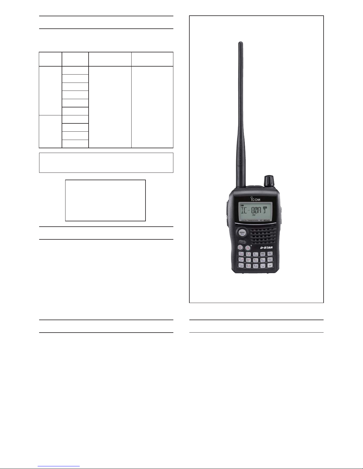
This service manual describes the latest technical
information for the IC-80AD and IC-E80D VHF/UHF
DIGITAL TRANSCEIVER at the time of publication.
NEVER connect the transceiver to an AC outlet or to a DC
power supply that uses more than specified. This will ruin
the transceiver.
DO NOT expose the transceiver to rain, snow or any liquids.
DO NOT reverse the polarities of the power supply when
connecting the transceiver.
DO NOT apply an RF signal of more than 20 dBm (100 mW) to
the antenna connector. This could damage the transceiver’s
front-end.
To upgrade quality, any electrical or mechanical parts
and internal circuits are subject to change without notice
or obligation.
MODEL VERSION
TYPE OF
EMISSION
Max. TX POWER
(VHF/UHF)
IC-80AD
[USA]
F2D, F3E, F7W 5 W/5 W
[SEA]
[CHN]
[KOR]
[AUS]
[EXP]
IC-E80D
[EUR]
[UK]
[ITR]
[FRA]
Be sure to include the following four points when ordering
replacement parts:
1. 10-digit Icom parts numbers
2. Component name
3. Equipment model name and unit name
4. Quantity required
<ORDER EXAMPLE>
1110003491 S.IC TA31136FNG IC-E80D/80AD MAIN UNIT 5 pieces
8820001210 Screw 2438 screw IC-E80D/80AD Top cover 10 pieces
Addresses are provided on the inside back cover for your
convenience.
Icom, Icom Inc. and ICOM logo are registered trademarks of Icom Incorporated (Japan) in the United States, the United
Kingdom, Germany, France, Spain, Russia and/or other countries.
ORDERING PARTS
1. Make sure that the problem is internal before
disassembling the transceiver.
2. DO NOT open the transceiver until the transceiver is
disconnected from its power source.
3. DO NOT force any of the variable components. Turn
them slowly and smoothly.
4. DO NOT short any circuits or electronic parts. An
insulated tuning tool MUST be used for all adjustments.
5. DO NOT keep power ON for a long time when the
transceiver is defective.
6. DO NOT transmit power into a Standard Signal
Generator or a Sweep Generator.
7. ALWAYS connect a 50 dB to 60 dB attenuator between
the transceiver and a Deviation Meter or Spectrum
Analyzer when using such test equipment.
8. READ the instructions of test equipment throughly
before connecting a test equipment to the transceiver.
REPAIR NOTES
INTRODUCTION
CAUTION
(IC-80AD)
UNIT ABBREVIATIONS:
F=FRONT UNIT
L=LOGIC UNIT
M=MAIN UNIT
V=VCO UNIT
R=RF UNIT
Page 3

TABLE OF CONTENTS
SECTION 1 SPECIFICATIONS
SECTION 2 INSIDE VIEWS
SECTION 3 DISASSEMBLY INSTRUCTION
SECTION 4 CIRCUIT DESCRIPITON
4-1 RECEIVER CIRCUITS. . . . . . . . . . . . . . . . . . . . . . . . . . . . . . . . . . . . . . . . . . . . . . . . . . . . . . . . 4-1
4-2 TRANSMITTER CIRCUITS . . . . . . . . . . . . . . . . . . . . . . . . . . . . . . . . . . . . . . . . . . . . . . . . . . . . 4-4
4-3 FREQUENCY SYNTHESIZER CIRCUITS . . . . . . . . . . . . . . . . . . . . . . . . . . . . . . . . . . . . . . . . 4-5
4-4 CPU (LOGIC UNIT: IC1) PORT ALLOCATION . . . . . . . . . . . . . . . . . . . . . . . . . . . . . . . . . . . . . 4-6
4-5 VOLTAGE BLOCK DIAGRAM . . . . . . . . . . . . . . . . . . . . . . . . . . . . . . . . . . . . . . . . . . . . . . . . . . 4-7
SECTION 5 ADJUSTMENT PROCEDURE
5-1 PREPARATION . . . . . . . . . . . . . . . . . . . . . . . . . . . . . . . . . . . . . . . . . . . . . . . . . . . . . . . . . . . . . 5-1
5-2 FREQUENCY ADJUSTMENT . . . . . . . . . . . . . . . . . . . . . . . . . . . . . . . . . . . . . . . . . . . . . . . . . . 5-3
5-3 IDLING CURRENT ADJUSTMENT (at 5.0 V) . . . . . . . . . . . . . . . . . . . . . . . . . . . . . . . . . . . . . . 5-3
5-4 IDLING CURRENT ADJUSTMENT (at 7.4 V) . . . . . . . . . . . . . . . . . . . . . . . . . . . . . . . . . . . . . . 5-4
5-5 IDLING CURRENT ADJUSTMENT (at 13.5 V) . . . . . . . . . . . . . . . . . . . . . . . . . . . . . . . . . . . . . 5-5
5-6 TRANSMIT POWER ADJUSTMENT (at 5.0 V). . . . . . . . . . . . . . . . . . . . . . . . . . . . . . . . . . . . . 5-6
5-7 TRANSMIT POWER ADJUSTMENT (at 7.4 V). . . . . . . . . . . . . . . . . . . . . . . . . . . . . . . . . . . . . 5-6
5-8 TRANSMIT POWER ADJUSTMENT (at 13.5 V). . . . . . . . . . . . . . . . . . . . . . . . . . . . . . . . . . . . 5-7
5-9 DEVIATION ADJUSTMENTS . . . . . . . . . . . . . . . . . . . . . . . . . . . . . . . . . . . . . . . . . . . . . . . . . . 5-8
5-10 TONE DEVIATION ADJUSTMENTS . . . . . . . . . . . . . . . . . . . . . . . . . . . . . . . . . . . . . . . . . . . . . 5-9
5-11 RECEIVE SENSITIVITY ADJUSTMENT . . . . . . . . . . . . . . . . . . . . . . . . . . . . . . . . . . . . . . . . . . 5-10
5-12 S-METER ADJUSTMENT . . . . . . . . . . . . . . . . . . . . . . . . . . . . . . . . . . . . . . . . . . . . . . . . . . . . . 5-12
SECTION 6 PARTS LIST
SECTION 7 MECHANICAL PARTS
SECTION 8 BOARD LAYOUTS
SECTION 9 BLOCK DIAGRAM
SECTION 10 VOLTAGE DIAGRAM
LOGIC UNIT . . . . . . . . . . . . . . . . . . . . . . . . . . . . . . . . . . . . . . . . . . . . . . . . . . . . . . . . . . . . . . . 10-1
MAIN UNIT. . . . . . . . . . . . . . . . . . . . . . . . . . . . . . . . . . . . . . . . . . . . . . . . . . . . . . . . . . . . . . . . . 10-3
RF UNIT. . . . . . . . . . . . . . . . . . . . . . . . . . . . . . . . . . . . . . . . . . . . . . . . . . . . . . . . . . . . . . . . . . . 10-5
VCO UNIT . . . . . . . . . . . . . . . . . . . . . . . . . . . . . . . . . . . . . . . . . . . . . . . . . . . . . . . . . . . . . . . . . 10-7
Page 4

1 - 1
SECTION 1. SPECIFICATIONS
Version
TX RX
U.S.A. 144–148, 420–450*
1
0.495–823.990,
849–868.990,
894–999.990
S.E.A.
CHN
EXP
137–174*
2
, 400–470*2 0.495–999.990
KOR 144–146, 430–440 144–146, 430–440
AUS 144–148, 420–450*
2
0.495–999.990
*
1
Guaranteed 440–450 MHz only, *2Guaranteed 430–440 MHz only
• Mode :
FM, FN-N, AM (Rx only), WFM (Rx only), DV
• No. of memory channels : 1052
(incl. 50 scan edges and 2 call channels)
• Usable temp. range : –20°C to +60°C; –4°F to +140°F
• Tuning steps : 5‡, 6.25‡, 8.33‡, 9‡, 10, 12.5, 15‡, 20,
25, 30, 50, 100, 125 and 200 kHz
D General
Version
TX RX
U.S.A. 144–148, 420–450*
1
0.495–823.990,
849–868.990,
894–999.990
S.E.A.
CHN
EXP
137–174*
2
, 400–470*2 0.495–999.990
KOR 144–146, 430–440 144–146, 430–440
AUS 144–148, 420–450*
2
0.495–999.990
*
1
Guaranteed 440–450 MHz only, *2Guaranteed 430–440 MHz only
All stated specifications are subject to change without notice or obligation.
• Frequency stability : ±2.5 ppm
(–20°C to +60°C; –4°F to +140°F)
• Power supply : 10.0–16.0 V DC for external DC power,
or specified Icom’s battery pack
• Digital transmission speed : 4.8 kbps
• Voice coding speed : 2.4 kbps
• Current drain (at 7.4 V DC) :
Tx High 144 MHz 1.8 A typical
430/440 MHz 2.1 A typical
Tx Mid. 144 MHz 1.2 A typical
430/440 MHz 1.5 A typical
Tx Low 144 MHz 0.6 A typical
430/440 MHz 0.7 A typical
Tx S-Low 144 MHz 0.4 A typical
Rx Rated output 170 mA typical
(FM)
215 mA typical (DV)
Power save 30 mA typical (FM)
(Duty 1:4)
38 mA typical (DV)
standby 62 mA typical (FM)
106 mA typical (DV)
• Antenna connector : SMA (50 Ω)
• Dimensions : 58.4(W)×103(H)×34.2(D) mm;
(projections not included) 25⁄16(W)×41⁄16(H)×111⁄32(D) in
• Weight (approx.) : 290 g; 10.3 oz (with antenna and BP-217)
D Transmitter
• Modulation system :
FM Variable reactance freq. modulation
DV (Digital) GMSK reactance freq. modulation
• Output power (at 7.4 V DC)
(Typical) : High 5.0 W, Mid. 2.5 W, Low 0.5 W,
S-Low 0.1 W
• Max. frequency deviation : ±5.0 kHz (FM wide: approx.)
±2.5 kHz (FM narrow: approx.)
• Spurious emissions : Less than –60 dBc at High/Mid.
Less than –13 dBm at Low/Slow
• Ext. mic. impedance : 2 kΩ
D Receiver
• Receive system :
Except WFM Double-conversion superheterodyne
WFM Triple-conversion superheterodyne
• Intermediate frequencies :
1st 61.65 MHz/59.25 MHz
(WFM only)
2nd 450 kHz/13.35 MHz (WFM only)
3rd 1.95 MHz (WFM only)
• Sensitivity (except spurious points):
FM
(1 kHz/3.5 kHz Dev.; 12 dB SINAD)
1.625–29.995 MHz 0.4 μV typ.
30.000–75.995 MHz 0.25 μV typ.
76.000–117.995 MHz 0.25 μV typ.
118.000–173.995 MHz 0.14 μV typ.
174.000–259.995 MHz 0.32 μV typ.
260.000–349.995 MHz 0.32 μV typ.
350.000–469.995 MHz 0.16 μV typ.
470.000–599.995 MHz 0.32 μV typ.
600.000–999.990 MHz 0.56 μV typ.
WFM
(1 kHz/52.5 kHz Dev.; 12 dB SINAD)
76.000–108.000 MHz 1 μV typ.
175.000–221.995 MHz 1.8 μV typ.
470.000–770.000 MHz 2.5 μV typ.
AM
(1 kHz/30% Mod.; 10 dB S/N)
0.495–4.995 MHz 1.3 μV typ.
5.000–29.995 MHz 0.56 μV typ.
118.000–137.000 MHz 0.5 μV typ.
222.000–246.995 MHz 0.79 μV typ.
247.000–329.995 MHz 1 μV typ.
DV
(PN9/GMSK 4.8ksps; BER 1%)
VHF (Amateur band only) 0.22 μV typ.
UHF
(Amateur band only) 0.22 μV typ.
• A
udio output power : More than 300 mW at 10% distortion
(at 7.4 V DC) with an 8 Ω load
• Selectivity :
FM
(Wide), AM More than 50 dB
FM (Narrow), DV More than 45 dB
WFM More than 300 kHz/–3 dB
Less than 700 kHz/–20 dB
• Ext. speaker connector : 3-conductor 3.5(d) mm; (1⁄8˝)/8 Ω
• Spurious and image rejection ratio :
VHF More than 60 dB
UHF More than 50 dB
(Intermediate freq.; More than 60 dB)
• Squelch Sensitivity (except spurious points):
FM (1 kHz/3.5 kHz Dev.)
1.625–29.995 MHz 0.4 μV typ.
30.000–75.995 MHz 0.25 μV typ.
76.000–117.995 MHz 0.25 μV typ.
118.000–173.995 MHz 0.14 μV typ.
174.000–259.995 MHz 0.32 μV typ.
260.000–349.995 MHz 0.32 μV typ.
350.000–469.995 MHz 0.16 μV typ.
470.000–599.995 MHz 0.32 μV typ.
600.000–999.990 MHz 0.56 μV typ.
WFM
(1 kHz/52.5 kHz Dev.)
76.000–108.000 MHz 1 μV typ.
175.000–221.995 MHz 1.8 μV typ.
470.000–770.000 MHz 2.5 μV typ.
AM (1 kHz/30% Mod.)
0.495–4.995 MHz 1.3 μV typ.
5.000–29.995 MHz 0.56 μV typ.
118.000–137.000 MHz 0.5 μV typ.
222.000–246.995 MHz 0.79 μV typ.
247.000–329.995 MHz 1 μV typ.
<For IC-80AD>
<F
or IC-E80D>
‡
Selectable depending on the operating
frequency band.
(unit: MHz)
(unit: MHz)
Page 5
2 - 1
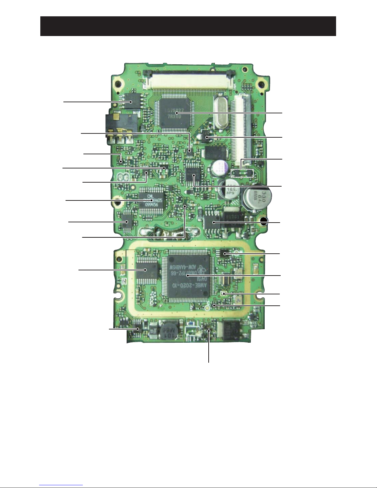
SECTION 2. INSIDE VIEWS
• LOGIC UNIT
VCC LINE SWITCH
(IC104)
EEPROM
(IC51)
ALC AMP
(IC300)
DIGITAL/ANALOG
MODE SWITCH
(IC303)
AF FILTER
(IC501 )
AF BUFERF
(IC504)
LINEAR CODEC
(IC503)
+5 V SWITCHING REGULATOR
(IC102)
AF MUTE SWITCHES
(Q403, 404)
IDC
(IC302)
3.3V REGULATOR
(Q507)
MIC GAIN SWITCH
(Q303)
MIC LINE SWITCH
(IC301)
1/2 DIVIDER
FOR MODEM CLOCK
(IC500)
AF POWER AMP
(IC400)
CPU3V REGULATOR
(IC100)
LCD DRIVER
(IC603)
DSP CODEC
(IC506)
DSP CLOCK AMP
(IC505)
BUFFER for DSP CLOCK
(IC505)
Page 6
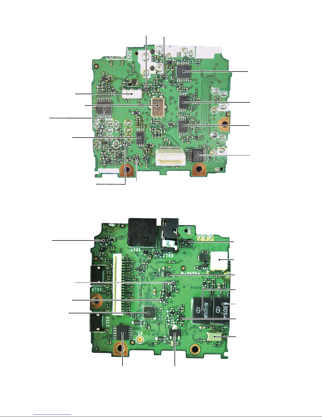
2 - 2
• MAIN UNIT
(TOP VIEW)
• MAIN UNIT
(BOTTOM VIEW)
SERIAL/PARALLEL
CONVERTER
(IC701)
AF FILTER
(IC501)
TONE FILTER
(IC150)
RX AF LINE SWITCH
(IC500)
REFERENCE FREQUENCY
SIGNAL BUFFER
(Q450)
SERIAL/PARALLEL
CONVERTER
(IC702)
T5V REGULATOR
(Q804)
2ND IF FILTER (WIDE/NARROW)
SELECTOR
(Q153)
IF IC
(IC100)
1ST IF FILTER (WFM)
(FI2)
1ST IF FILTER (FM/AM/DV)
(FI50)
CURRENT DETECT
(IC800)
2ND IF FILTER
(WIDE MODE)
(FI200)
D/A CONVERTER
(IC600)
RF AMP
(Q700)
2ND IF AMP (WFM)
(Q1)
2ND IF MIXER (WFM)
(Q2)
FM/WFM MODE SWITCH
(Q201)
DISCRIMINATOR
(X100)
T5V REGULATOR
(Q805)
REFERENCE FREQUENCY
OSCILLATOR
(X450)
2ND IF FILTER
(NARROW MODE)
(FI100)
DETECT VOLTAGE
SELETCOR
(BATTERY/DC-IN)
(IC1000)
AGC VOLTAGE DETECTOR
(Q104)
IF AMP
(Q103)
Page 7
1 - 1
TX POWER AMPLIFIER
(Q100)
VCO UNIT
• RF UNIT
R3V LINE SWITCH
(Q251, 303, 703)
HV LINE SWITCH
(Q1000)
RF CIRCUITS SHIFT SWITCH
(Q252, 302)
TX LO AMPLIFIER
(IC100)
Page 8
FLAT
CABLE
LOGIC unit
A
B
B
B
B
Front panel
E
D
B
B
B
A
C
Rear panel
A
A
A
D
D
B
B
B
RF UNIT
Rear panel
C
RF UNIT
Rear panel
MAIN UNIT
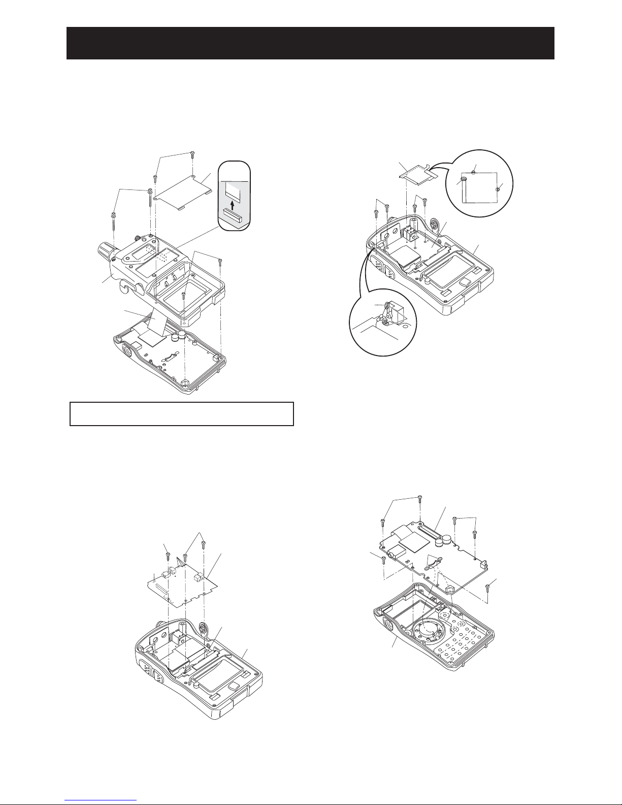
3 - 1
1. Removing the rear panel
q Unscrew 2 screws A and remove the plate B.
w Unscrew 2 screws C and 2 screws D.
e Disconnect the flat cable E from MAIN UNIT.
r Remove the rear panel.
3. Removing the RF UNIT
q Unsolder 2 points A.
w Unsolder 3 points B and remove the shield plate C.
e Unscrew 4 screws D and remove the RF UNIT from the
rear panel.
2. Removing the MAIN UNIT
q Unsolder 5 points A.
w Unscrew 3 screws B.
e Remove the MAIN UNIT from the rear panel.
4. Removing the LOGIC UNIT
1 Unsolder 2 points A.
2 Unscrew 6 screws B and remove the LOGIC UNIT
from the front panel.
SECTION 3. DISASSEMBLY INSTRUCTION
BE CAREFUL about the fl at cable and connector when
separating the CHASSIS UNIT from the FRONT UNIT.
Page 9

4 - 1
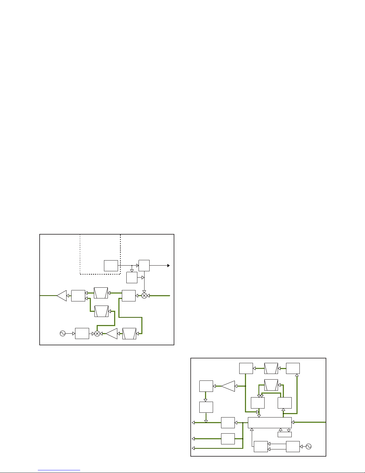
SECTION 4. CIRCUIT DESCRIPTION
4-1 RECEIVER CIRCUITS
RF CIRCUITS (RF UNIT)
RX signals from the antenna are sorted by its frequency by
the filters and gone through RF circuits for each bands.
• 76 MHz and below
The RX signals are passed through two LPFs, ANT SW,
band SW and LPF. The RX signals are sorted by its
frequency by band SWs.
• 0.495–29.995 MHz
The RX signals are passed through the band SW (D201)
and LPF, and applied to tuned RF AMP (Q200). The
amplified RX signals are applied to the 1st mixer (IC900) via
two band SWs (D203 and D707).
• 30–75.995 MHz
The RX signals are passed through the band SW (D250) and
tuned BPF, and applied to the RF AMP (Q250). The amplified
RX signals are passed through tuned BPF, then applied to
the 1st IF mixer (IC900) via two band SWs (D256 and D707).
• 76–117.995 MHz
The RX signals are passed through two LPFs, ANT SW, band
SW (D300), LPF and another band SW (D301) in sequence,
then applied to the RF AMP (Q300) via the tuned BPF. The
amplified RX signals are passed through another tuned BPF,
then applied to another RF AMP (Q301). The amplified RX
signals are applied to the 1st mixer (IC900) via two band SWs
(D311
and D707
).
• 118–173.995 MHz
The RX signals are passed through two LPFs, ANT SW, and
band SW (D400), then applied to the RF AMP (Q400). The
amplified RX signals are passed through the tuned BPF, and
applied to another RF AMP (Q401). The amplified RX signals
are passed through tuned BPF, then applied to the 1st IF
mixer (IC900) via two band SWs (D405 and D509).
• 174–259.995 MHz
The RX signals are passed through the LPF, HPF, ANT
SW, ATT, band SW (D302), HPF and another band SW in
sequence, then applied to the RF AMP (Q300) via the tuned
BPF. The amplified RX signals are passed through another
tuned BPF, then applied to another RF AMP (Q301). The
amplified RX signals are applied to the 1st mixer (IC900) via
two band SWs (D311 and D707).
• 260–349.995 MHz and 470–599.995 MHz
The RX signals are passed through the LPF, HPFANT SW,
ATT, BAND SW and tuned BPF in sequence, then applied to
the RF AMP (Q500). The amplified RX signals are passed
through another 2-pole tuned BPF, and applied to another
RF AMP (Q501). The amplified RX signals are then applied
to the 1st mixer (IC900) via two band SWs
(D508 and
D707)
.
• 350–469.995 MHz
The RX signals are passed through the LPF, HPF, ANT
SW, ATT, band SW and HPF in sequence, then applied to
the RF AMP (Q600). The amplified RX signals are passed
through the tuned BPF, and applied to the RF AMP (Q601).
The amplified RX signals are passed through the BPF, then
applied to the 1st mixer (IC900) via two band SWs (D606
and D707).
• 600–999.990 MHz
The RX signals are passed through the HPF, ATT and
applied to the RF AMP (Q700). The amplified RX signals
are passed through the tuned BPF, and applied to another
RF AMP (Q701). The amplified RX signals are applied to
the 1st mixer (IC900) via the band SWs (D706 and D707).
The RF attenuation which reduces RX signal level to –10 dB is
carried out by D5, D9 and D701, by turning these PIN diodes
ON using "ATT" signal.
RF
AMP
ANT
SW
RF
AMP
RF
AMP
LPF
BAND
SW
BPF
BAND
SW
RF
SW
RF
AMP
RF
SW
LPF
BAND
SW
BPF
RF
AMP
HPF
BPF
HPF
BPF
BAND
SW
RF
AMP
LPF
BANDSWRF
AMP
RF
AMP
BPF
LPF
RF
AMP
BAND
SW
ATT
LPF
BAND
SW
BPF
BPF
BAND
SW
RF
AMP
ANT
SW
BAND
SW
BAND
SW
BAND
SW
BAND
SW
BPF
BAND
SW
BAND
SW
BPF
BAND
SW
BPF
RF
AMP
RF
AMP
HPF
BPF
Q1,2,150
D1,3,4,10,151,160
Q1,3,D6-8
RF UNIT
D304,305
Q601
D604,605
D606
D400
Q401
Q701
D402,403
D405
D200
D250
D254,255
D508
D253
D705
D603
D311
Q400
Q700
D201
Q500
D252
D600
D300
Q300
D302
D401
D703,704
D404
D706
D500
Q200
D503
D251
D256
Q600
D301
D306-309
Q301
D303
D 700
D501,502
D203
BAND
SW
D203
D504,507
Q250
Q501
D202
D601,602
To 1st mixer
(IC900)
for A BAND
From the VHF TX
circuits
From the UHF TX
circuits
D310
0.5−30 MHz
30−76 MHz
Tx: 430.000−450.000 MHz
Tx: 144.000−148.000 MHz
174−260 MHz
76−118 MHz
118−174MHz
470−600 MHz
260−350 MHz
350−470 MHz
600−1000MHz
HPF
L1-3
C1-6
L4,C7-9
L200,201
C201-204
L300,301
C301-305
L600,608
C600-602,630,631
L8,9
C18-20
L302,303
C306-310
L202,203
C205-9
L5-7
C10-14
• RF CIRCUITS
Page 10
4 - 2
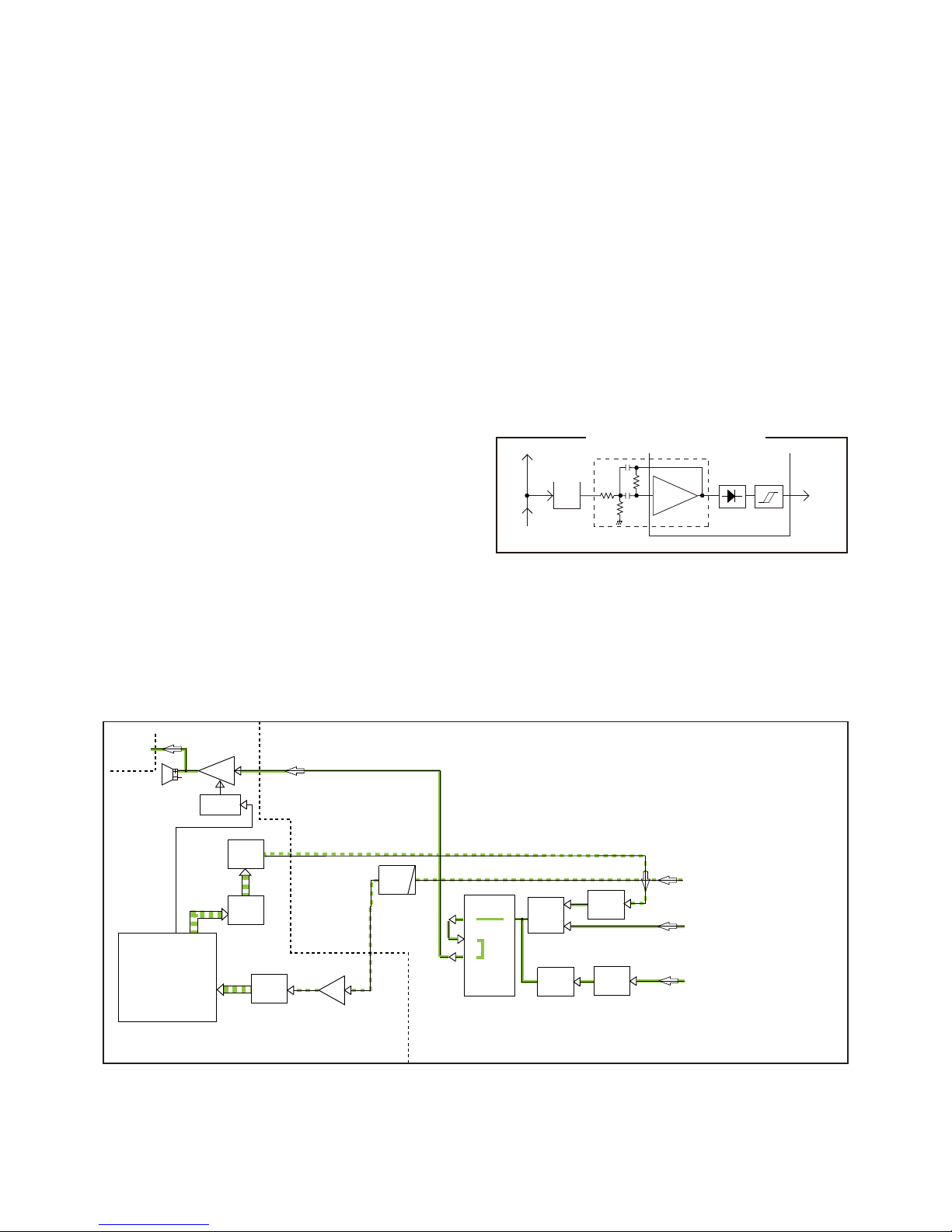
1ST IF CIRCUIT (MAIN UNIT)
The RX signals from the RF circuits are applied to the 1st
mixer (RF: IC900) to be converted into the 1st IF signal,
by being mixed with the 1st Local Oscillator (LO) signals
from the VCO UNIT. The 1st LO signals from the VCO UNIT
are applied to the 1st mixer via the LO SW, or doubler (in
receiving of 600 MHz and above).
The converted 1st IF signal is passed through the IF SW (D2)
which toggles the path of the 1st IF signal: WFM mode or
other than WFM mode.
• FM/AM/DV MODE
The 1st IF signal from the 1st mixer (RF: IC900) is entered
to the MAIN UNIT, and passed through the 1st IF filter (FI50)
via IF SWs (D2, 3) to remove unwanted signals. The filtered
1st IF signals are applied to the 1st IF AMP (Q100), and the
amplified 1st signal is applied to the 2nd IF circuit.
• WFM MODE (Incl. 2nd IF circuit)
When receiving in WFM mode, the 1st IF signal from the 1st
mixer (RF: IC900) is entered to the MAIN UNIT and passed
through the IF SW (D2) and BPF, then applied to the 1st IF
AMP (Q1). The amplified 1st IF signal is applied to the 2nd
mixer (Q2) to converted into the 13.35 MHz 2nd IF signal,
by being mixed with the 45.9 MHz 2nd LO signal (generated
by X450, tripled by Q451). The converted 2nd IF signal is
passed through the 2nd IF filter (FI2) to remove sideband
noise, then applied to the 2nd IF AMP (Q100) via the IF SW
(D3). The amplified 2nd IF signal is applied to the 3rd IF
circuit.
2ND IF AND DEMODULATOR CIRCUITS (MAIN UNIT)
<For FM, AM and DV mode>
The 1st IF signal from the 1st IF AMP (Q100) is applied to
the IF IC (IC100). The applied 1st IF signal is mixed with
the 61.2 MHz 2nd LO signal (generated by X450, buffered
by Q452) at the internal 2nd mixer, to be converted into the
450 kHz 2nd IF signal. The converted 2nd IF signal is output
from pin 3.
• FM MODE
The 2nd IF signal from the IF IC is passed through the 2nd
IF filter (FI100) via IF SWs (D102, 103). The filtered 2nd
IF signal is backed to the IF IC from pin 5, and saturationamplified by the internal limit AMP. The amplified 2nd IF
signal is FM-demodulated by the discriminator (X100), and
the recovered AF signals (RX AF signals) are output from
pin 9, then applied to the AF circuits via the FM mode SW
(IC500D, pins 8, 9).
• AM MODE
The 2nd IF signal from the IF IC is passed through the 2nd
IF filter (FI200) via IF SWs (D150, 151). The filtered 2nd IF
signal is amplified by 2nd IF AMP (Q103), then applied to
the AM demodulator circuit (Q104) to be recovered to the
AF signals. The demodulated AF signals are applied to the
AF circuits via the AM mode SW (IC500A).
• DV MODE
The 2nd IF signal from the IF IC is passed through the 2nd
IF filter (FI100) via IF SWs (D102, 103). The filtered 2nd
IF signal is backed to the IF IC from pin 5, then saturationamplified by the internal limit AMP. The amplified 2nd IF
signal is FM-demodulated by the discriminator (X200), and
the recovered AF signals (RX AF signals) are output from
pin 9, then applied to the AF circuits via the AF mute SW
(IC500, pins 4, 3).
• 3RD IF CIRCUIT (MAIN UNIT)
<For WFM mode only>
The 2nd IF signal from the 2nd IF AMP (Q100) is applied to
the IF IC.
The applied 2nd IF signal is mixed with the 15.3 MHz 3rd
LO signal (generated by X450, buffered by Q452), to be
converted into the 1.95 MHz 3rd IF signal by the internal 3rd
mixer. The converted 3rd IF signal is output from pin 3, and
passed through the IF SWs (D105, 106), then backed to the
IF IC (bypassing FI100). The 3rd IF signal is FM-demodulated
by the discriminator (X100), and the recovered AF signals
(RX AF signals) are output from pin 9, then applied to the AF
circuits via the WFM mode SW (IC500C, pins 8, 9).
X2
BPF
XTAL
LO
SW
BPF
CERAMIC
IF
AMP
VCOs
From the RF
circuits
IF
AM
P
BPF
SW
MODE
MAIN UNIT
SW
MODE
15.3MHz
Reference frequency
oscillator
FM/AM/DV:61.65 MH
z
WFM:13.35 MH
z
TX circuits
D100
Q850
IC900
1st IF mixer
D2
FI2
FI50
D3
Q100
To the IF IC
(IC100)
X450
VCO UNIT
D850
BC BAND; Q1,2,D1-3,5,6
VHF BAND; Q51,52,D51-55
UHF BAND; Q101,102,D100-104
X3
Q451
Q2
BPF
CERAMIC
BPF
CERAMIC
IF
AMP
AM
DET
SW
MODE
FM
DET
DISCRI
MODE
MAIN UNIT
SW
MODE
SW
FM61.2MHz
WFM15.3MHz
From the IF AMP (Q100)
X1
or
X4
Q452D450
FI200
FI100
SW
MODE
SW
MODE
D150D151
D102
Q103
Q104
SW
MODE
IC500A
To the AF filter
(IC501)
To the mode Sw
(IC501)
To the buffer
(IC504B)
SW
MODE
IC500D
SW
MODE
IC500C
AM
FM
WFM
IC100
X100
15.3MHz
X450
D105
D106
D103
• 1ST IF CIRCUIT
• 2ND IF AND DEMODULATOR CIRCUITS
Page 11
4 - 3
RX AF CIRCUITS (LOGIC UNIT)
• FM/W-FM/AM MODE
The AF signals from the FM/AM demodulator circuits are
passed through the mode SW (MAIN UNIT: IC500D/C/A)
and one of the AF filters whose audio frequency response
is set as stable for each RX mode (FM/AM or WFM).
FM/AM-demodulated AF signals are filtered by IC501, and
FM-demodulated AF signals (W-FM mode) are filtered by
Q552.
The filtered AF signals are passed through the D/A
converter (MAIN UNIT: IC600, pins 15, 14; 16, 17) for level
adjustment. The level-adjusted AF signals are entered to the
LOGIC UNIT, and applied to the AF power AMP (IC400) to
obtain audio output power. The power-amplified AF signals
are applied to the internal speaker or output from the [SP]
jack.
• DV MODE
The FM-demodulated signals from the IF IC (MAIN UNIT:
IC100) are applied to the modem (IC501) via the LPF and
buffer (IC504B), to be converted into the DV data. The DV
data is applied to the CPU (IC1), and converted into the
AMBE signals. The AMBE signal is then applied to the DSP
CODEC IC (IC506) and decoded. The decoded AMBE
signals are converted into the analog audio signal by liner
CODEC IC (IC503). The converted AF signals are passed
through the mode SW (MAIN UNIT: IC500B) and AF filter
(MAIN UNIT: IC501A).
The filtered AF signals are passed through the D/A
converter (MAIN UNIT: IC600, pins 15, 14; 16, 17) for level
adjustment. The level-adjusted AF signals are entered to the
LOGIC UNIT, and applied to the AF power AMP (IC400) to
obtain audio output power. The power-amplified AF signals
are applied to the internal speaker or output from the [SP]
jack.
SP
AF
AMP
BUFF
LPF
CPU
Q400-402
POWER AMP
CONTROLLER
MODEM
DSP
CODEC
LINEAR
CODEC
IC600
IC400
LOGIC UNIT MAIN UNIT
CHASSIS
[SP]
IC503
IC506
IC504B
IC501
IC1
IC501
SW
SW
FIL
IC500A
MODE
IC500D
MODE
<FM/AM/ MODE>
AM/FM-demodulated AF signals from
AM mode SW (IC500A)/FM mode SW (IC500D)
<WFM MODE>
FM-demodulated AF signals from
WFM mode SW (IC500C)
<DV MODE>
FM-demodulated AF signals from
IF IC (IC100)
AF
D/A
AFON
AF
FIL
Q552
15
4
3
8
11
2
6
1
14
6711
20,21
16
17
2
6
DAC
Noise
AMP
Noise filter
From IF IC
(IC100, Pin16)
To RX AF circuits
Noise
detector
Com-
parator
NOISE SQUELCH DIAGRAM
“NOIS”
IC600
IC100
9
8
7
13
10
SQUELCH CIRCUIT
The squelch circuit cuts off the AF output signals when
no RF signals are received. Detecting noise components
(approx. 30 kHz signals) in the demodulated AF signals, the
squelch circuit stops audio signals being emitted.
A portion of FM-demodulated AF signal from the IF IC (MAIN
UNIT: IC100) is passed through the DAC (MAIN UNIT:
IC600) for level (=threshold) adjustment. The level-adjusted
AF signals are passed through the noise filter (IC100, pins 7,
8 and R111–113, C121, 122) to filter the noise components
(approx. 30 kHz signals) only. The noise components are
rectified to produce DC voltage corresponding to the noise
level.
If the noise level is higher than the preset one, the internal
comparator set the "NOISE" signal to the CPU to "High",
then the CPU turns the "AFON" signal which controlls the
AF power AMP (L: IC400) to "Low," to inactivate the AF
power AMP (L: IC400). At the same time, the CPU turns the
"RMUTE" signal which controlls the AF mute SW (L: Q403,
404) to "Low," to cut-off the RX AF line.
• RX AF CIRCUITS
Page 12
4 - 4
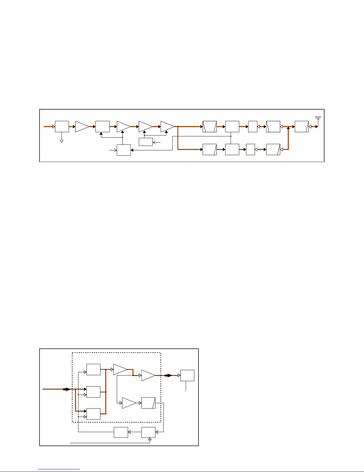
4-2 TRANSMITTER CIRCUITS
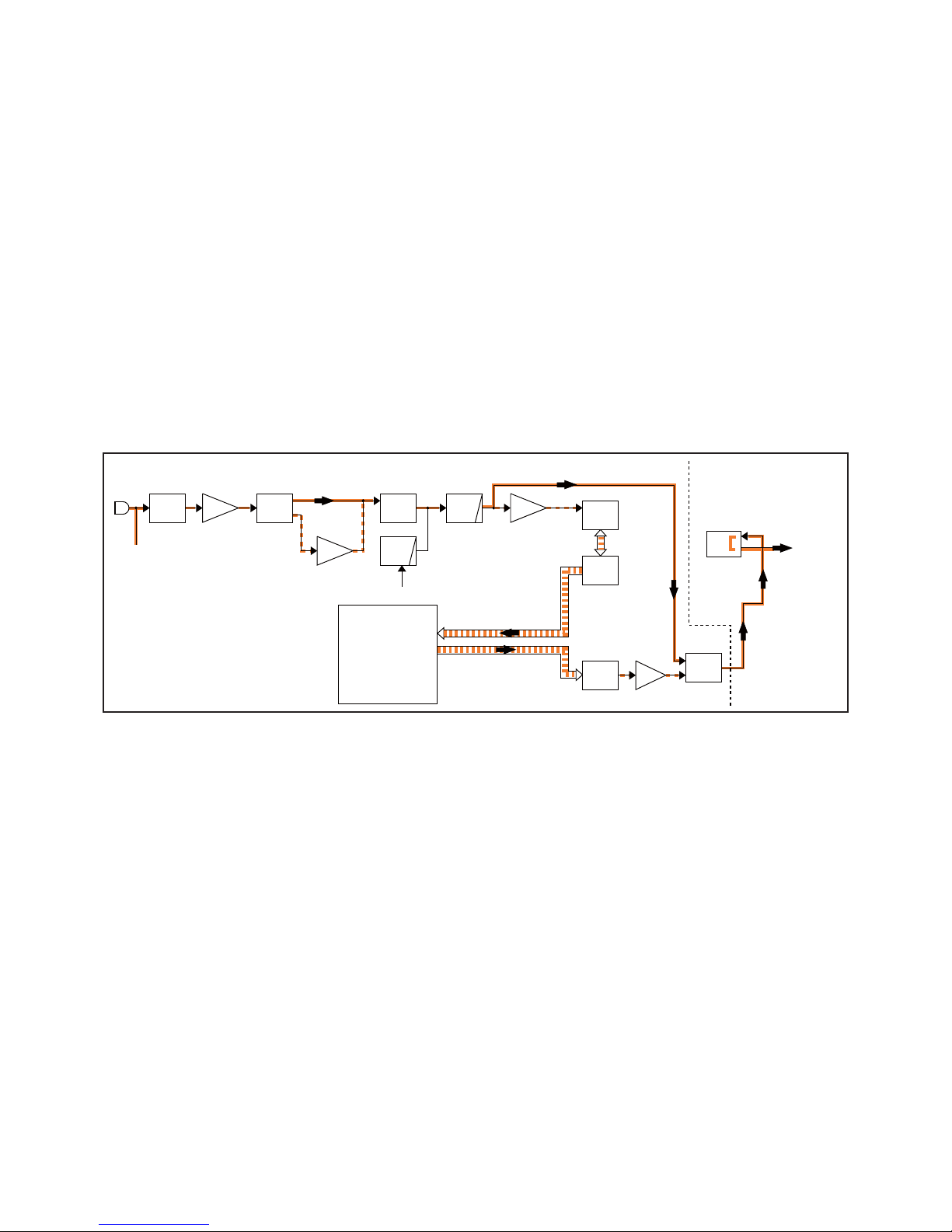
TX AF CIRCUITS (LOGIC UNIT)
• FM MODE
MIC signals from the internal/external microphone (MIC
signals) are passed through the MIC gain SW (Q303),
and applied to the MIC AMP (Q302, 304). The amplified
MIC signals are passed through the mode SW (IC301)
which toggles the MIC line according to the operating
mode; FM or DV. The MIC signals are applied to the IDC
(Instance Deviation Controller; IC302B) circuit which limits
the amplitude of MIC signals (=deviation) to prevent over
deviation.
The amplitude-limited MIC signals are passed through
the splatter filter (IC302C) which cuts off the 3 kHz and
higher audio signals. The frequency-limited MIC signals are
entered to the MAIN UNIT via the mode SW (IC303), then
applied to the DAC (MAIN UNIT: IC600) for level (=deviation)
adjustment. The level-adjusted MIC signals are applied to
the modulation circuits.
• DV MODE
The MIC signals from the microphone (MC300) are passed
through the MIC gain SW (Q303) and applied to the MIC
AMP (Q302, 304). The amplified MIC signals are applied
to the ALC AMP (IC300) which automatically adjusts the
level of MIC signals to stable for digital processing, via
the mode SW (IC301). The level-adjusted MIC signals are
applied to the IDC circuit (IC302B) for amplitude-limiting.
The amplitude-limited MIC signals are passed through the
splatter filter (IC302C) which cuts off the 3 kHz and higher
audio signals.
The frequency-limited MIC signals are applied to the liner
CODEC IC (IC503) via the buffer (IC504A), and encoded
into the digital audio signal. The digital audio signal is then
applied to the DSP CODEC IC (IC506) and converted into
the AMBE signal. The AMBE signal is applied to the modem
IC (IC501) via the CPU (IC1). The modem IC converts the
AMBE signal into the analog signal, and output to the DAC
(IC600, pin 1) via the buffer (IC302D) and the mode SW
(IC303). The tone signal is level-adjusted by DAC (MAIN
UNIT: IC600), then applied to the modulation circuits as the
modulation signals.
MODULATION CIRCUITS (VCO UNIT)
The modulation signals from the DAC (MAIN UNIT: IC600,
pin 2) are entered to the VCO UNIT, and applied to the
variable capacitors of VCOs.
• OPERATING ON VHF BAND
The modulation signals are applied to the D55 of the VHF
VCO (Q51, 52, D51–55) to obtain FM modulation. The
FM-modulated VCO output is buffer-amplified by Q200,
amplified by Q201 then entered to the RF UNIT as TX
signal.
• OPERATING ON UHF BAND
The modulation signals are applied to the D100 of the UHF
VCO (Q101, 102, D100–104) to obtain FM modulation. The
FM-modulated VCO output is buffer-amplified by Q200,
amplified by Q201 then entered to the RF UNIT as TX
signal.
TX AMPLIFIERS (RF UNIT)
TX signal from VCO UNIT is applied to the LO AMP
(IC100) via the LO SW (D100). The amplified TX signal is
passed through the ATT (D101, 102) which is a port of the
APC circuit. The level-adjusted TX signal is amplified by
YGR (Q102), drive (Q101) and power (Q100) amplifiers in
sequence, to obtain TX output power. The power-amplified
TX signal is passed through the TX filters, power detector
and ANT SWs.
• OPERATION ON VHF BAND
The power-amplified TX signal from the power AMP (Q100)
is passed through the LPF, ANT SW (D9, 61, 62), power
detector (D59, 60) and two LPFs (as a harmonic filter), then
applied to the antenna via ANT connector (CHASSIS; J1).
• OPERATION ON UHF BAND
The power-amplified TX signal from the power AMP (Q100)
is passed through the BPF, power detector (D50, 53), ANT
SW, HPF and LPF (as a harmonic filter), then applied to the
antenna via ANT connector (CHASSIS; J1).
Modulation signals
to the VCO UNIT
MC300
MIC
AMP
BUFF
BUFF
LPF
IDC
LPF
SPLATTER
ALC
AMP
CPU
MODEM
DSP
CODEC
LINEAR
CODEC
SW
MODE
IC302B
IC302C
IC302D
IC600
Q306,307
Q309
LOGIC UNIT
IC503
IC504A
IC506
IC501,502
IC3
MAIN UNIT
D/A
Q302,304
MODE
SW
IC301
IC300
CTCSS
SW
GAIN
IC303
Q303
From ext. microphone
1
6
7
1
2
1
6
5
7
98
5
21
?
?
12
14
7
• TX AF CIRCUITS
Page 13
4 - 5
ATT
ANT
SW
PWR
DET
PWR
AMP
LPF
LPF
APC
CTRL
YGR
AMP
DRIVE
AMP
LPF
GATE
CTRL
HPF
TX/RX
SW
PWR
DET
ANT
SW
LO
AMP
BPF
D101,102
IC150B
PSET
D59,60
Q100Q102
D50,53
Q101
IC100
D100,850
IC150A
Q152
L1-3
C1-6
L100.101.153
C100-103,192
L102,103
C106,107
L5-7
C10-14
L4,C7-9
ANT
Q153
D154-156
D150,152,153
DSET
VHF TX signal
UHF TX signal
FILTER
LOOP
VCO
BUFF
BUFF
TX/RX
SW
PLL
IC
VCO
LO
AMP
VCO
LPF
RF UNIT
Q201
D850
IC800
UHF BAND:
319.175-538.345 MHz
VCO UNIT
Q101,102,D100-104
Q1,2,D1-3,5,6
Q51,52,D51-55
Q200
BC BAND: 62.145−131.645 MHz
Q202
1st LO signals
(A BAND)
D100
VHF BAND:
131.350-235.645 MHz
15.3MHz reference frequency
Modulation signals
APC CIRCUIT (RF UNIT)
The APC (Automatic Power Control) circuit stabilizes
transmit output power to prevent transmit output power level
change which is caused by load mismatching or heat effect,
etc.
TX signal is passed through the power detector (VHF; D59,
60/UHF; D50, 53). The power detector rectifies a portion
of the TX signal and converts it into DC voltage which is in
proportion to the transmit output power. The detected voltage
is applied to the APC controller (IC150B). The TX power
setting voltage “PSET” is applied to another input terminal as
the reference voltage.
The output voltage is applied to the ATT (D101, 102) to control the attenuation level, to adjust the input level of the YGR
AMP (Q102) so that the TX output power is stable.
The setting of TX power is carried out by applying voltage
“PSET” to the APC controller (IC150B).
The output voltage of
the controller controls the bias of the drive and power AMPs
to reduce/increase the gain of these amplifi ers to set the TX
output power to High, Mid., Low and S-Low.
4-3 FREQUENCY SYNTHESIZER CIRCUITS
VCOs
This transceiver has total of five VCOs; one RX VCO and
RX/TX VCOs on the VCO UNIT, and two RX VCOs on the
MAIN UNIT.
• BC BAND VCO (VCO UNIT; Q1, D1, 3, 5, 6)
The BC BAND VCO generates the 1st LO for BC band
(0.495–75.995 MHz) RX.
• VHF BAND VCO (VCO UNIT; Q51, D51, 54)
The VHF BAND VCO generates the 1st LO for VHF band
(76–173.995 MHz) RX, and also TX signal for the operation
on the VHF band.
• UHF BAND VCO (VCO UNIT; Q101, D101–104)
The UHF BAND VCO generates the LO for UHF band (174–
599.995 MHz) RX, and also TX signal for the operation on
the UHF band.
When receiving 600 MHz and higher signals, the UHF BAND
VCO oscillates 269.175–469.17 MHz 1st LO signals, and the
output signal is doubled by the doubler (MAIN UNIT; Q850,
D851) before being applied to the mixer (MAIN UNIT; IC900).
PLL (VCO AND MAIN UNITS)
The PLL circuit provides stable oscillation for both of the
transmit and 1st LO frequencies. By comparing the fedback
VCO output and the reference frequency signal, the oscillating
frequency is stabilized. The PLL output frequency is controlled
by the serial data including divide ratio from the CPU.
A portion of output signals from each VCO are fedback
to the PLL IC (MAIN UNIT: IC800) via buffers (VCO:
Q200, 202) and LPF. The applied VCO outputs are divided
by the prescaler and programmable divider, then phasecompared with divided reference frequency from X450
(MAIN). The phase difference is output via the charge pump,
and applied to the VCOs as lock voltage via the loop filter.
When the oscillation frequency drifts, its phase changes
from that of the reference frequency, causing a lock voltage
change to compensate for the drift in the VCO oscillating
frequency.
• TX AMPLIFIERS AND APC CIRCUIT
• FREQUENCY SYNTHESIZER CIRCUITS
Page 14

4 - 6
PIN
No.
LINE
NAME
DESCRIPTION
IN/
OUT
STATUS CONDITION
3 PCON
Transceiver power control.
OUT H
While the transceiver power is
ON.
4 AFMUTE AF mute signal to the AF mute SW (LOGIC UNIT: Q403, 404). OUT H AF mute.
5 MUTE TX mute signal. OUT H TX mute.
6 MICC
MIC AMP (LOGIC UNIT: Q304) control signal to the MIC AMP controller
(LOGI UNIT: Q302).
OUT L MIC AMP is activated.
7 AFON
Control signal to the AF power AMP controller (LOGIC UNIT: Q400–402).
OUT H
AF power AMP (L: IC400) is
activated (Squelch open).
9BATT
Power supply select signal to the power supply selector (LOGIC UNIT:
IC1000).
OUT H/L
H= Operated by the battery
pack.
L= Operated by an external
power source.
10,
11
MIC1, MIC2
MIC gain control signals to the MIC gain controller (LOGIC UNIT: Q303).
OUT – –
12 ACQ ACQ signal to the modem (LOGIC UNIT: IC501). OUT H Synchronized.
14 RXDT RX data to the modem (LOGIC UNIT: IC501). IN – –
15 TXDT TX data to the modem (LOGIC UNIT: IC501). OUT – –
16 AMBEC DSP IC power line regulator (LOGIC: IC508) control signal. OUT H In DV mode operation.
18 DVC
Liner CODEC IC power line regulator (LOGIC UNIT: Q503, 504) control
signal.
OUT H In DV mode operation.
20 PTT [PTT] key input. (Pull-down) IN H The key is pushed.
21 DASTB2 Strobe signal to the DAC (MAIN UNIT: IC600). OUT – –
26 BTDET Battery attach detect. IN L A battery is attached.
27 RXCK RX clock to the modem (LOGIC UNIT: IC501). IN – –
28 TXCK TX clock to the modem (LOGIC UNIT: IC501). IN – –
34 LINH LCD driver (LOGIC UNIT: IC603) chip-enable signal. OUT L LCD display OFF.
35 LCE Strobe signal to the LCD driver (LOGIC UNIT: IC603). OUT – –
36 LDI Serial data to the LCD driver (LOGIC UNIT: IC603). OUT – –
37 LCL Clock to the LCD driver (LOGIC UNIT: IC603). OUT – –
38 BLED
[BUSY] LED driver (LOGIC UNIT: Q201) control signal.
OUT H
While receiving (Squelch
open).
39 TXLED TX LED control signal. OUT H Lights ON. (While transmitting)
40 LLIGHT LCD backlight control signal. OUT L Backlight ON.
41 KLIGHT LCD/Key backlight driver (LOGIC UNIT: Q201) control signal. OUT L Lights ON.
42 AMBECLK AMBE clock signal to the DSP CODEC IC (LOGIC UNIT: IC506). OUT – –
43 AMBERXD AMBE RX data to the DSP CODEC IC (LOGIC UNIT: IC506). IN – –
44 AMBETXD AMBE TX data to the DSP CODEC IC (LOGIC UNIT: IC506). OUT – –
45 AMBESTB AMBE strobe signal to the DSP CODEC IC (LOGIC UNIT: IC506). OUT – –
46 NOIS Noise detect signal from the IF IC (MAIN UNIT: IC100). IN – –
47 AMBERES
Reset signal to the liner CODEC IC and DSP CODEC IC (LOGIC UNIT:
IC503 and IC506).
OUT – –
49 AMBEEPR AMBEEPR signal to the DSP CODEC IC (LOGIC UNIT: IC506). IN – –
50 DTCS Tone fi lter response switching signal. OUT H DTCS signals is in use.
51–
55
KR0–KR4
Key detect signal.
(Pushed button is detected according to the input voltage.)
IN – –
56 SQL [SQL] key input. (Pull-up) IN L The key is pushed.
57 DIUD [DIAL] input (Phase B). IN – –
59 DICK [DIAL] input (Phase A). IN – –
61–
64
KS0–KS3
Key matrix ports.
OUT – –
69 IOSTB Strobe signal to the expander (RF UNIT: IC951). OUT – –
70 IOSTB1 Strobe signal to the expanders (MAIN UNIT: IC701, 702). OUT – –
71 IOEN Output enable signal to the expanders (MAIN UNIT: IC701, 702). OUT – –
72 DASTB1 Strobe signal to the DAC (RF UNIT: IC950). OUT – –
73 PLLSTB Strobe signal to the PLL IC (MAIN UNIT: IC800). OUT – –
7 4 DATA
Common serial data to the PLL ICs and DAC (LMX2313/ME15E03SL/
M62352AGP).
OUT – –
75 CK
Common clock signal to the the PLL ICs and DAC (LMX2313/
ME15E03SL/M62352AGP).
OUT – –
4-4 CPU (LOGIC UNIT: IC1) PORT ALLOCATION
Page 15
4 - 7
4-4 CPU PORT ALLOCATION (continued)
4-5 VOLTAGE BLOCK DIAGRAM
Voltage from the power supply is routed to the whole of the transceiver via regulators and switches.
DC-IN VCC +5V +3CPU
DC
SW
SW
REG
V3+
T
Q1000,
D1000, 1001
IC102
Q803−805
Q400−402
IC100
Q800, 801
IC103
Q150−153
D150, 151
TAB
Battery pack
T5
NOCP
CHGH CHGC
TXC
VCO UNIT
BCVCOC
VVCOC
UVCOC
AF PWR AMP
(IC400)
AFON
AMBEC
CHG
T5
AF AMP
REG
REG
3.3V
REG
3.2V
REG
+5V
SW
+3V
3.2V
5V
DVC
+5V
REG
+3V
REG
VCO3V
SW
V5.5+
IC125
DC-DC
PIN
No.
LINE
NAME
DESCRIPTION
IN/
OUT
STATUS CONDITION
77 RESET
Reset signal from the reset IC (LOGIC UNIT: IC100).
IN H –
79 UNLK Unlock signal from the PLL IC (MAIN UNIT: IC800). IN H PLL is locked.
85 RX232 RS-232 data (RXD). IN – –
86 TX232 RS-232 data (TXD). OUT – –
89 CLSFT
Clock frequency shift signal to the clock oscillator (LOGIC UNIT: X1,
D13).
OUT H –
90 PPS Power save mode control signal to theD PLL IC (MAIN UNIT: IC800). OUT L In power save mode.
91 CHGC
Charging control signal to the charge circuit (LOGIC UNIT: Q150–153,
D150, 151)
OUT H While charging.
92 CHGH
Charging current control signal to the charging controller (LOGIC UNIT:
Q150, 152).
OUT H Charging current increase.
97 TEMP
The voltage in proportion to the internal temperature.
The voltage divided by R66 (thermistor; LOGIC UNIT) and R67 (LOGIC
UNIT).
IN – –
98 RTONE Weather alert signals. IN – –
96 VIN
DC voltage divided by the voltage detect resisters (LOGIC UNIT: R159
and R160). (Remaining battery capacity detection.)
IN – –
99 CTONE CTCSS signals. IN – –
100 RSSI RSSI voltage from the IF IC (MAIN UNIT: IC100). IN – –
101 TX-V
• While operated by batteryRSSI voltage from the IF IC (MAIN UNIT:
IC100).
• While perated by external power supplyCurrent in TX from the I-V
converter (MAIN UNIT: IC800).
IN – –
102 TTEMP
The voltage in proportion to the TX power AMP (RF UNIT: Q100)
temperature.The voltage divided by R161 (thermistor; RF UNIT) and
R162 (RF UNIT).
IN – –
103 CTCOUT CTCSS/DTCS signals. OUT – –
104 DTMF Tone (DTMF, european tone: IC-E80D only) signals. OUT – –
109 CPUHV
External power supply detection.
IN L
External power supply is
connected.
110 POWER [POWER] key input. (Pull-up) IN L The key is pushed.
111 D_AS Analog/Digital mode switching signal. IN H Analog mode.
113 ECK Clock to the EEPROM (LOGIC UNIT: IC51). OUT – –
114 ESIO
Serial data to the EEPROM (LOGIC UNIT: IC51). IN/
OUT
––
116 CLIN Key detect signal. (Pushed button is detected by refering input voltage.) IN – –
118 CLOUT Cloning data. OUT – –
Page 16
5 - 1
SECTION 5. ADJUSTMENT PROCEDURE
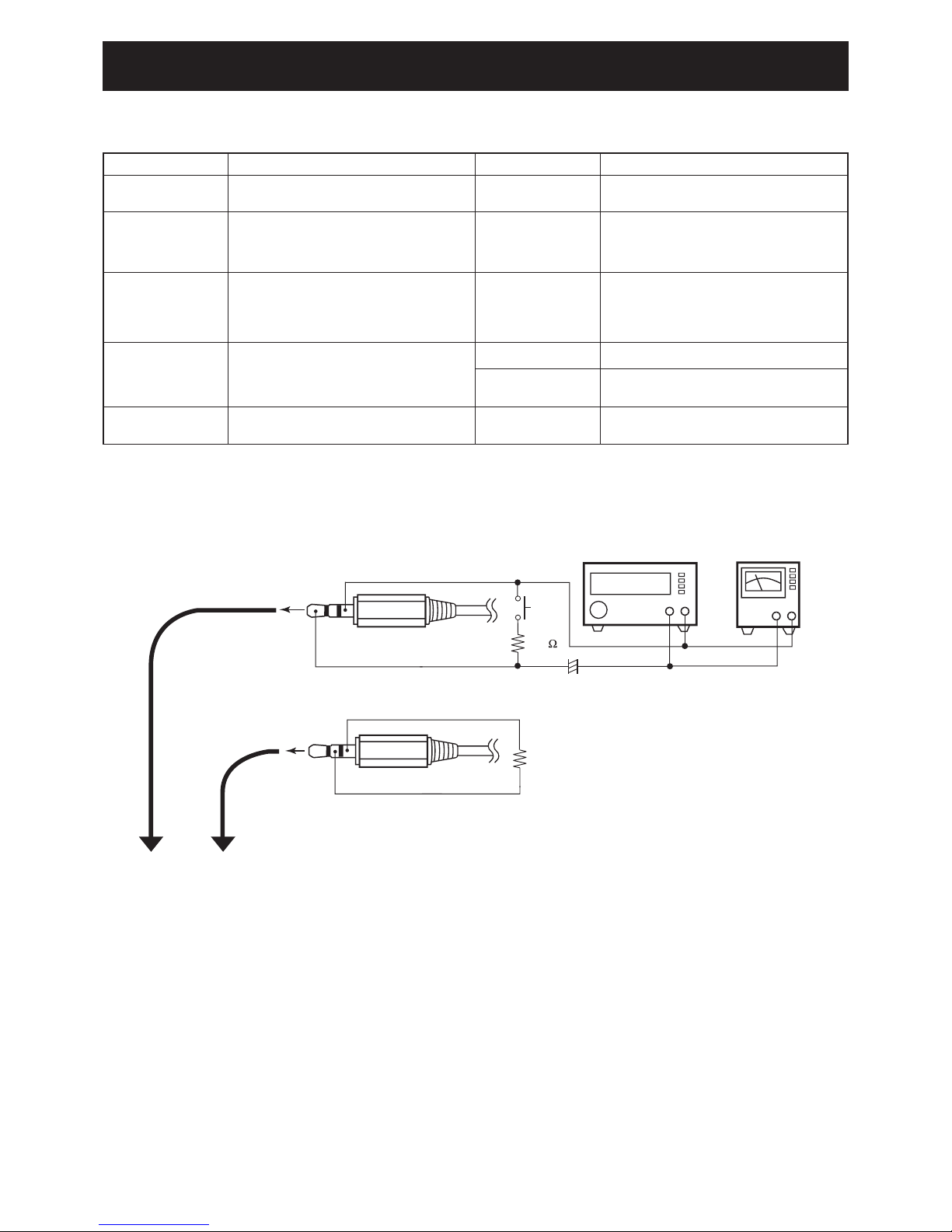
5-1 PREPARATION
¤ REQUIRED INSTRUMENTS
INSTRUMENTS SPECIFICATION INSTRUMENTS SPECIFICATION
DC Cables
• OPC-254L (Optional product)
• Connects to battery terminals
JIG cables
(See the illust below)
Power Supply
Output voltages : 13.5 V DC
7.4 V DC
5.0 V DC
Current capacity : More than 3 A
Multimeter
Input impedance : 50 kΩ
Measuring range : 0.1–10V/0.01–5 A
RF Power Meter
(terminated type)
Measuring range : 0.1–10 W
Frequency range : 100–500 MHz
Impedance : 50
Ω
SWR : Less than 1.2 : 1
Standard Signal
Generator (SSG)
Frequency range : 0.1–1200 MHz
Output level : –20 to 90 dBµ
(–127 to 90 dBm)
Frequency Counter
Frequency range : 0.1–600 MHz
Frequency accuracy : ±1 ppm or better
Input level : Less than 1 mW
AC Millivoltmeter Measuring range : 10 mV to 10 V
Attenuator
Power attenuation : 30 dB
Capacity : More than 10 W
Modulation
Analyzer
Frequency range : 30–600 MHz
Measuring range : 0 to ±10 kHz
Audio Generator
Frequency range : 300–3000 Hz
Output level : 1–500 mV
3-conductor 2.5 (d) mm
[MIC]
To [MIC] jack
[SP]
plug
(MIC)
(GND)
33 k
+−
AC
MILLIVOLTMETER
(10 mV to 10 V)
AUDIO GENERATOR
(300–3000 Hz/1–500 mV)
+−
PTT
+
4.7 µF
3-conductor 3.5 (d) mm plug
(CLONE)
(GND)
68 kΩ
To [SP] jack
M JIG CABLES
Page 17

5 - 2
Frequency
Adjustment item
Transmit power
Mode
Selects next adjustment item
Stores the value for the adjustment
Selects previous adjustment item
Adjusts the value for the item
JIG cables
(See the page 5-1)
To the [DC IN] jack
OPC-254L
:etihW
:kcalB
DC power supply
13.5 V/3 A
DC power supply
5.0 or 7.4 V/3 A
Be sure the polarity.
• Adjustments at 5.0 V and 7.4 V
• Adjustments at 13.5 V
POWER SUPPLY
JIG cables
(See the page 5-1)
Modulation analyzer
(DC measurable)
Attenuator
30 dB or 40 dB
to the antenna connector
Standard signal generator
–20 to 90 dBµ
(–127 to –17 dBm)
CAUTION:
DO NOT transmit while
SSG is connected to
the antenna connector.
RF power meter
6 W
Frequency
counter
Oscilloscope
M ENTERING ADJUSTMENT MODE
q Turn the transceiver power OFF.
w Connect
JIG cables (See the page 5-1) to the [MIC] and [SP] jacks.
e Push and [SQL] and [8], turn the transceiver power ON.
Entering adjustment mode, the function display shows the adjustment item and conditions as below.
M CONNECTION
M
QUITTING ADJUSTMENT MODE
q Turn the transceiver power OFF.
w Disconnect the JIG cable, then turn the power OFF.
Page 18

5 - 3
5-2 FREQUENCY ADJUSTMENT
Select an adjustment item using [2] / [8], then set the adjustment value as specifi ed using [DIAL].
ADJUSTMENT
ADJUSTMENT
ITEM
OPERATION VALUE
REFERENCE
FREQUENCY
[FR]
1 1) Set the power supply voltage to 7.4 V.
2) Connect an RF power meter to the antenna connector.
3) Loose couple a frequency counter to the antenna connector.
4) While transmitting, adjust the frequency using [DIAL], then push
[BAND] to store the adjustment value.
440.0000
MHz
(±200 Hz)
5-3 IDLING CURRENT ADJUSTMENT (at 5.0 V)
Select an adjustment item using [2] / [8], then set the adjustment value as specifi ed using [DIAL].
ADJUSTMENT
ADJUSTMENT
ITEM
OPERATION VALUE
DRIVE AMP
IDLING CURRENT
[ID5]
1 1) Set the power supply voltage to 5.0 V.
2) Connect an RF power meter to the antenna connector.
3) Connect a multimeter between the power supply and transceiver.
4) Set the item [IP5] to "00."
–
[VHF BAND]
2• While transmitting, adjust the idling current using [DIAL], then
push [BAND] to store the adjustment value.
180–230
mA
[UHF BAND]
3 150–200
mA
FINAL AMP
IDLING CURRENT
[IP5]
1 1) Set the power supply voltage to 5.0 V.
2) Connect an RF power meter to the antenna connector.
3) Connect a multimeter between the power supply and transceiver.
–
[VHF BAND]
2• While transmitting, adjust the idling current using [DIAL], then
push [BAND] to store the adjustment value.
200–300
mA
[UHF BAND]
3
NOTE: When "IDLING CURRENT" is adjusted, "TRANSMIT POWER" must be re-adjusted too.
Page 19

5 - 4
5-4 IDLING CURRENT ADJUSTMENT (at 7.4 V)
Select an adjustment item using [2] / [8], then set the adjustment value as specifi ed using [DIAL].
ADJUSTMENT
ADJUSTMENT
ITEM
OPERATION VALUE
DRIVE AMP
IDLING CURRENT
[ID7]
1 1) Set the power supply voltage to 7.4 V.
2) Connect an RF power meter to the antenna connector.
3) Connect a multimeter between the power supply and transceiver.
4) Set the item [IP7] to "00."
–
[VHF BAND]
(Hi power)
2• While transmitting, adjust the idling current using [DIAL], then
push [BAND] to store the adjustment value.
180–230
mA
(Mid power)
3
(Low power)
4
(S-Low power)
5
[UHF BAND]
(Hi power)
6
150–200
mA
(Mid power)
7
(Low power)
8
(S-Low power)
9
FINAL AMP
IDLING CURRENT
[IP7]
1 1) Set the power supply voltage to 7.4 V.
2) Connect an RF power meter to the antenna connector.
3) Connect a multimeter between the power supply and transceiver.
–
[VHF BAND]
(Hi power)
2• While transmitting, adjust the idling current using [DIAL], then
push [BAND] to store the adjustment value.
1.15 A
(Mid power)
3
650 mA
(Low power)
4
250 mA
(S-Low power)
5
[UHF BAND]
(Hi power)
6
1.15 A
(Mid power)
7 650 mA
(Low power)
8
250 mA
(S-Low power)
9
NOTE: When "IDLING CURRENT" is adjusted, "TRANSMIT POWER" must be re-adjusted too.
Page 20

5 - 5
5-5 IDLING CURRENT ADJUSTMENT (at 13.5 V)
Select an adjustment item using [2] / [8], then set the adjustment value as specifi ed using [DIAL].
ADJUSTMENT
ADJUSTMENT
ITEM
OPERATION VALUE
DRIVE AMP
IDLING CURRENT
[ID1]
1 1) Set the power supply voltage to 13.5 V.
(supplying from [DC IN])
2) Connect an RF power meter to the antenna connector.
3) Connect a multimeter between the power supply and transceiver.
4) Set the item [IP1] to "00."
–
[VHF BAND]
(Hi power)
2• While transmitting, adjust the idling current using [DIAL], then
push [BAND] to store the adjustment value.
180–230
mA
(Mid power)
3
(Low power)
4
(S-Low power)
5
[UHF BAND]
(Hi power)
6
150–200
mA
(Mid power)
7
(Low power)
8
(S-Low power)
9
FINAL AMP
IDLING CURRENT
[IP1]
1 1) Set the power supply voltage to 13.5 V.
(supplying from [DC IN])
2) Connect an RF power meter to the antenna connector.
3) Connect a multimeter between the power supply and transceiver.
–
[VHF BAND]
(Hi power)
2• While transmitting, adjust the idling current using [DIAL], then
push [BAND] to store the adjustment value.
700 mA
(Mid power)
3
400 mA
(Low power)
4
250 mA
(S-Low power)
5
[UHF BAND]
(Hi power)
6
900 mA
(Mid power)
7 400 mA
(Low power)
8
250 mA
(S-Low power)
9
NOTE: When "IDLING CURRENT" is adjusted, "TRANSMIT POWER" must be re-adjusted too.
Page 21

5 - 6
5-6 TRANSMIT POWER ADJUSTMENT (at 5.0 V)
Select an adjustment item using [2] / [8], then set the adjustment value as specifi ed using [DIAL].
ADJUSTMENT
ADJUSTMENT
ITEM
OPERATION VALUE
TRANSMIT
POWER
[PO5]
1 1) Set the power supply voltage to 5.0 V.
2) Connect an RF power meter to the antenna connector.
3) While transmitting, adjust the TX power using [DIAL], then push
[BAND] to store the adjustment value.
80–120
mW
[VHF (BAND LOW)] 2
[VHF (BAND HIGH)] 3
[UHF (BAND LOW)] 4
[UHF (BAND HIGH)] 5
5-7 TRANSMIT POWER ADJUSTMENT (at 7.4 V)
Select an adjustment item using [2] / [8], then set the adjustment value as specifi ed using [DIAL].
ADJUSTMENT
ADJUSTMENT
ITEM
OPERATION VALUE
TRANSMIT POWER
[PO7]
1 1) Set the power supply voltage to 7.4 V.
2) Connect an RF power meter to the antenna connector.
–
(Hi power)
[VHF (BAND LOW)]
2• While transmitting, adjust the TX power using [DIAL], then push
[BAND] to store the adjustment value.
4.8–5.2 W
[VHF (BAND HIGH)]
(Hi power)
[UHF (BAND LOW)]
3
5.0–5.4 W
[UHF (BAND HIGH)]
4.6–5.0 W
(Mid power)
[VHF (BAND LOW)]
4
2.3–2.7 W
[VHF (BAND HIGH)]
(Mid power)
[UHF (BAND LOW)]
5
[UHF (BAND HIGH)]
(Low power)
[VHF (BAND LOW)]
6
0.4–0.6 W
[VHF (BAND HIGH)]
(Low power)
[UHF (BAND LOW)]
7
[UHF (BAND HIGH)]
(S-Low power)
[VHF (BAND LOW)]
8
80–120
mW
[VHF (BAND HIGH)]
(S-Low power)
[UHF (BAND LOW)]
9
[UHF (BAND HIGH)]
Page 22

5 - 7
5-8 TRANSMIT POWER ADJUSTMENT (at 13.5 V)
Select an adjustment item using [2] / [8], then set the adjustment value as specifi ed using [DIAL].
ADJUSTMENT
ADJUSTMENT
ITEM
OPERATION VALUE
TRANSMIT POWER
–
1 1) Set the power supply voltage to 13.5 V.
(supplying from [DC IN])
2) Connect an RF power meter to the antenna connector.
–
(Hi power)
[VHF (BAND LOW)]
[PO1]
2• While transmitting, adjust the TX power using [DIAL], then push
[BAND] to store the adjustment value.
4.8–5.2 W
[VHF (BAND HIGH)]
3
(Hi power)
[UHF (BAND LOW)]
4
5.0–5.4 W
[UHF (BAND HIGH)]
5 4.6–5.0 W
(Mid power)
[VHF (BAND LOW)]
6
2.3–2.7 W
[VHF (BAND HIGH)]
7
(Mid power)
[UHF (BAND LOW)]
8
[UHF (BAND HIGH)]
9
(Low power)
[VHF (BAND LOW)]
10
0.4–0.6 W
[VHF (BAND HIGH)]
11
(Low power)
[UHF (BAND LOW)]
12
[UHF (BAND HIGH)]
13
(S-Low power)
[VHF (BAND LOW)]
14
80–120
mW
[VHF (BAND HIGH)]
15
(S-Low power)
[UHF (BAND LOW)]
16
[UHF (BAND HIGH)]
17
Page 23

5 - 8
5-9 DEVIATION ADJUSTMENTS
Select an adjustment item using [2] / [8], then set the adjustment value as specifi ed using [DIAL].
ADJUSTMENT
ADJUSTMENT
ITEM
OPERATION VALUE
FM DEVIATION
[FMV]
1 1) Set the power supply voltage to 7.4 V.
1) Connect a modulation analyzer to the antenna connector through
an attenuator, and set is as;
HPF : OFF
LPF : 20 kHz
De-emphasis : OFF
Detector : (P-P)/2
2) Connect an audio generator to the JIG cable (See the page 5-1).
–
(Mod. Freq. =1 kHz)
[VHF (BAND LOW)]
2 1) Set the audio generator as;
Frequency : 1 kHz
Level : 90 mVrms
2) While transmitting, adjust the deviation using [DIAL], then push
[BAND] to store the adjustment value.
4.1–4.3 kHz
[VHF (BAND HIGH)]
3
[UHF (BAND LOW)]
4
[UHF (BAND HIGH)]
5
(Mod. Freq. =300 Hz)
[VHF (BAND LOW)]
[FMR]
1 1) Set the audio generator as;
Frequency : 300 Hz
Level : 90 mVrms
2) While transmitting, adjust the deviation using [DIAL], then push
[BAND] to store the adjustment value.
3.5–3.6 kHz
[VHF (BAND HIGH)]
2
[UHF (BAND LOW)]
3
3.7–3.8 kHz
[UHF (BAND HIGH)]
4
DV DEVIATION
–
1 1) Set the power supply voltage to 7.4 V.
1) Connect a modulation analyzer to the antenna connector through
an attenuator, and set is as;
HPF : OFF
LPF : 20 kHz
De-emphasis : OFF
Detector : (P-P)/2
2) Connect an audio generator to the JIG cable (See the page 5-1),
and set it as;
Frequency : 1 kHz
Level : 90 mVrms.
–
(VCO MODULATION)
[VHF (BAND LOW)]
[DVV]
2• While transmitting, adjust the deviation using [DIAL], then push
[BAND] to store the adjustment value.
1.1–1.3 kHz
[VHF (BAND HIGH)]
3
[UHF (BAND LOW)]
4
[UHF (BAND HIGH)]
5
(REF. MODULATION)
[VHF (BAND LOW)]
[DVR]
6
Minimum
deviation
[VHF (BAND HIGH)]
7
[UHF (BAND LOW)]
8
[UHF (BAND HIGH)]
9
Page 24

5 - 9
5-10 TONE DEVIATION ADJUSTMENTS
Select an adjustment item using [2] / [8], then set the adjustment value as specifi ed using [DIAL].
ADJUSTMENT
ADJUSTMENT
ITEM
OPERATION VALUE
TONES DEVIATION
[DT]
1 1) Set the power supply voltage to 7.4 V.
2) Connect a modulation analyzer to the antenna connector through
an attenuator, and set is as;
HPF : OFF
LPF : 20 kHz
De-emphasis : OFF
Detector : (P-P)/2
3) No audio signals are applied.
–
[DTMF]
(VHF)
2• While transmitting, adjust the deviation using [DIAL], then push
[BAND] to store the adjustment value.
3.4–3.6 kHz
(UHF)
[EUROPEAN TONE]
(VHF)
[EUR]
3
(UHF)
[CTCSS]
(VHF)
[CT]
4
0.75–0.85
kHz
(UHF)
[DTCS]
(VHF)
[DTC]
5
0.7–0.8 kHz
(UHF)
Page 25

5 - 10
5-11 RECEIVE SENSITIVITY ADJUSTMENTS
1) Select an adjustment item (band) using [2] / [8].
2) Set the SSG as specifi ed (frequency, deviation and output level).
3) Push the [BAND] to adjust (automatic) and store the adjustment value.
ADJUSTMENT
ADJUSTMENT
ITEM
OPERATION VALUE
RECEIVE
SENSITIVITY
NOTE:
“RECEIVE SENSITIVITY” must be adjusted before “S-METER.” Otherwise, “S-METER” will
not be adjusted properly.
[Tr]
1 1) Set the power supply voltage to 7.4 V.
2) Connect an SSG to the antenna connector and set as;
Modulation : 1 kHz
Deviation : 3.5 kHz
Push
[BAND].
(Automatic
adjustment)
[30.1 MHz*]
2 • Set the SSG as;
Frequency : (Displayed on the function display)
Level : 0 dBµ (–107 dBm)
†
[49.9 MHz*]
3 • Set the SSG as;
Frequency : (Displayed on the function display)
Level : 0 dBµ (–107 dBm)
†
[50.1 MHz*]
4 • Set the SSG as;
Frequency : (Displayed on the function display)
Level : 0 dBµ (–107 dBm)
†
[75.9 MHz*]
5 • Set the SSG as;
Frequency : (Displayed on the function display)
Level : 0 dBµ (–107 dBm)
†
[76.1 MHz*]
6 • Set the SSG as;
Frequency : (Displayed on the function display)
Level : 0 dBµ (–107 dBm)
†
[90.2 MHz*]
7 • Set the SSG as;
Frequency : (Displayed on the function display)
Level : 0 dBµ (–107 dBm)
†
[117.9 MHz*]
8 • Set the SSG as;
Frequency : (Displayed on the function display)
Level : 0 dBµ (–107 dBm)
†
[118.1 MHz*]
9 • Set the SSG as;
Frequency : (Displayed on the function display)
Level : –3 dBµ (–110 dBm)
†
[146.1 MHz*]
10 • Set the SSG as;
Frequency : (Displayed on the function display)
Level : –3 dBµ (–110 dBm)
†
[173.9 MHz*]
11 • Set the SSG as;
Frequency : (Displayed on the function display)
Level : –3 dBµ (–110 dBm)
†
[174.1 MHz*]
12 • Set the SSG as;
Frequency : (Displayed on the function display)
Level : 0 dBµ (–107 dBm)
†
[222.1 MHz*]
13 • Set the SSG as;
Frequency : (Displayed on the function display)
Level : 0 dBµ (–107 dBm)
†
[259.9 MHz*]
14 • Set the SSG as;
Frequency : (Displayed on the function display)
Level : 0 dBµ (–107 dBm)
†
[260.2 MHz*]
15 • Set the SSG as;
Frequency : (Displayed on the function display)
Level : 0 dBµ (–107 dBm)
†
[305.2 MHz*]
16 • Set the SSG as;
Frequency : (Displayed on the function display)
Level : 0 dBµ (–107 dBm)
†
[349.9 MHz*]
17 • Set the SSG as;
Frequency : (Displayed on the function display)
Level : 0 dBµ (–107 dBm)
†
[350.1 MHz*]
18 • Set the SSG as;
Frequency : (Displayed on the function display)
Level : –3 dBµ (–110 dBm)
†
[440.1 MHz*]
19 • Set the SSG as;
Frequency : (Displayed on the function display)
Level : –3 dBµ (–110 dBm)
†
†
; This output level of a standard signal generator (SSG) is indicated as SSG’s open circuit.
*; This frequency is an example only, and may differ from the actual frequency displayed on the function display.
Page 26

5 - 11
5-11 RECEIVE SENSITIVITY ADJUSTMENT (continued)
1) Select an adjustment item (band) using [2] / [8].
2) Set the SSG as specifi ed (frequency, deviation and output level).
3) Push the [BAND] to adjust (automatic) and store the adjustment value.
ADJUSTMENT
ADJUSTMENT
ITEM
OPERATION VALUE
[469.9 MHz*]
[Tr]
20 • Set the SSG as;
Frequency : 469.9 MHz
Level : –3 dBµ (–110 dBm)
†
Push
[BAND].
(Automatic
adjustment)
[470.1 MHz*]
21 • Set the SSG as;
Frequency : 470.1 MHz
Level : 0 dBµ (–107 dBm)
†
[535.1 MHz*]
22 • Set the SSG as;
Frequency : 535.1 MHz
Level : 0 dBµ (–107 dBm)
†
[599.9 MHz*]
23 • Set the SSG as;
Frequency : 599.9 MHz
Level : 0 dBµ (–107 dBm)
†
[600.1 MHz*]
24 • Set the SSG as;
Frequency : 600.1 MHz
Level : 0 dBµ (–107 dBm)
†
[780.1 MHz*]
25 • Set the SSG as;
Frequency : 780.1 MHz
Level : 0 dBµ (–107 dBm)
†
[999.9 MHz*]
26 • Set the SSG as;
Frequency : 999.9 MHz
Level : 0 dBµ (–107 dBm)
†
†
; This output level of a standard signal generator (SSG) is indicated as SSG’s open circuit.
*; This frequency is an example only, and may differ from the actual frequency displayed on the function display.
Page 27

5 - 12
5-12 S-METER ADJUSTMENT
1) Select an adjustment item using [2] / [8].
2) Set the SSG as specifi ed (frequency, deviation and output level).
3) Push the [BAND] to adjust (automatic) and store the adjustment value.
ADJUSTMENT
ADJUSTMENT
ITEM
OPERATION VALUE
S-METER CURVE
NOTE:
“RECEIVE SENSITIVITY” must be adjusted before “S-METER CURVE” and “S-METER S3 LEVLE.”
Otherwise, “S-METER CURVE” and “S-METER S3 LEVLE will not be adjusted properly.
–
1 1) Set the power supply voltage to 7.4 V.
2) Connect an SSG to the antenna connector and set as;
Modulation : 1 kHz
Deviation : 3.5 kHz
–
[145.1 MHz* (S0 level)]
[S0]
2 • Set the SSG as;
Frequency : (Displayed on the function display)
Level : –8 dBµ (–115 dBm)
†
Push
[BAND].
(Automatic
adjustment)
[145.1 MHz* (S3 level)]
[S3]
• Set the SSG as;
Level : –6 dBµ (–113 dBm)
†
[145.1 MHz* (Full scale)]
[SF]
• Set the SSG as;
Level : –2 dBµ (–109 dBm)
†
[87.5 MHz* (S0 level)]
[S0]
3 • Set the SSG as;
Frequency : (Displayed on the function display)
Deviation : 52.5 kHz
Level : 2 dBµ (–105 dBm)
†
[87.5 MHz* (S3 level)]
[S3]
• Set the SSG as;
Level : 5 dBµ (–102 dBm)
†
[
87.5
MHz* (Full scale)]
[SF]
• Set the SSG as;
Level : 25 dBµ (–82 dBm)
†
S-METER S3 LEVEL
(FM)
[S3]
1 1) Set the power supply voltage to 7.4 V.
2) Connect an SSG to the antenna connector and set as;
Modulation : 1 kHz
Deviation : 3.5 kHz
–
[1.01 MHz*]
2 • Set the SSG as;
Frequency : (Displayed on the function display)
Level : –6 dBµ (–113 dBm)
†
Push
[BAND].
(Automatic
adjustment)
[15.1 MHz*]
3 • Set the SSG as;
Frequency : (Displayed on the function display)
Level : –8 dBµ (–115 dBm)
†
[40.1 MHz*]
4 • Set the SSG as;
Frequency : (Displayed on the function display)
Level : –6 dBµ (–113 dBm)
†
[60.1 MHz*]
5 • Set the SSG as;
Frequency : (Displayed on the function display)
Level : –6 dBµ (–113 dBm)
†
[220.1 MHz*]
6 • Set the SSG as;
Frequency : (Displayed on the function display)
Level : –6 dBµ (–113 dBm)
†
[305.2 MHz*]
7 • Set the SSG as;
Frequency : (Displayed on the function display)
Level : –6 dBµ (–113 dBm)
†
[435.1 MHz*]
8 • Set the SSG as;
Frequency : (Displayed on the function display)
Level : –6 dBµ (–113 dBm)
†
[535.1 MHz*]
9 • Set the SSG as;
Frequency : (Displayed on the function display)
Level : –6 dBµ (–113 dBm)
†
[800.1 MHz*]
10 • Set the SSG as;
Frequency : (Displayed on the function display)
Level : 0 dBµ (–107 dBm)
†
†
; This output level of a standard signal generator (SSG) is indicated as SSG’s open circuit.
*; This frequency is an example only, and may differ from the actual frequency displayed on the function display.
Page 28

5 - 13
5-12 S-METER ADJUSTMENT (continued)
1) Select an adjustment item using [2] / [8].
2) Set the SSG as specifi ed (frequency, deviation and output level).
3) Push the [BAND] to adjust (automatic) and store the adjustment value.
ADJUSTMENT
ADJUSTMENT
ITEM
OPERATION VALUE
S-METER S3 LEVEL
(WFM)
[1.01 MHz*]
[S3]
1 • Set the SSG as;
Frequency : (Displayed on the function display)
Deviation : 52.5 kHz
Level : 5 dBµ (–102 dBm)
†
Push
[BAND].
(Automatic
adjustment)
[15.1 MHz*]
2 • Set the SSG as;
Frequency : (Displayed on the function display)
Level : 3 dBµ (–104 dBm)
†
[40.1 MHz*]
3 • Set the SSG as;
Frequency : (Displayed on the function display)
Level : 5 dBµ (–102 dBm)
†
[60.1 MHz*]
4 • Set the SSG as;
Frequency : (Displayed on the function display)
Level : 5 dBµ (–102 dBm)
†
[220.1 MHz*]
5 • Set the SSG as;
Frequency : (Displayed on the function display)
Level : 5 dBµ (–102 dBm)
†
[305.2 MHz*]
6 • Set the SSG as;
Frequency : (Displayed on the function display)
Level : 5 dBµ (–102 dBm)
†
[435.1 MHz*]
7 • Set the SSG as;
Frequency : (Displayed on the function display)
Level : 5 dBµ (–102 dBm)
†
[535.1 MHz*]
8 • Set the SSG as;
Frequency : (Displayed on the function display)
Level : 5 dBµ (–102 dBm)
†
[800.1 MHz*]
9 • Set the SSG as;
Frequency : (Displayed on the function display)
Level : 11 dBµ (–96 dBm)
†
†
; This output level of a standard signal generator (SSG) is indicated as SSG’s open circuit.
*; This frequency may differ from the actual frequency displayed on the function display.
Page 29

6 - 1
SECTION 6. PARTS LIST
M.=Mounted side (T: Mounted on the Top side, B: Mounted on the Bottom side)
[RF UNIT]
REF PARTS
DESCRIPTION
M.
H/V
NO. NO.
LOCATION
IC100 1110006870 S.IC UPC2709TB-E3 T 34/14.3
IC150 1110006380 S.IC LM2904PWR T 43.8/34.7
IC151 1130013240 S.IC TC75S51FU(TE85L,F) B 45.2/18
IC152 1190001830 S.IC BH2220FVM-TR T 15.7/31.8
IC800 1130011671 S.IC MB15E03SLPFV1-G-ER-6E1 T 20.1/25.8
IC900 1110005230 S.IC UPC2757TB-E3 B 14.9/9.6
IC951 1130011760 S.IC CD4094BPWR B 6.8/8.9
IC952 1110006380 S.IC LM2904PWR T 8.5/28.8
Q2 1590002010 S.TRA XP1114(TX) T 30.5/32.5
Q3 1590003281 S.TRA UNR9211G0L T 29.7/27.3
Q4 1590003281 S.TRA UNR9211G0L T 29.7/29.3
Q50 1590003281 S.TRA UNR9211G0L B 33.6/36.7
Q100 1560001151 S.FET 2SK3476(TE12L,Q) T 39/27.7
Q101 1560001161 S.FET 2SK3475(TE12L,F) T 46.6/20.4
Q102 1530000371 S.TRA 2SC3356-T1B S (R25) T 41.4/17.3
Q200 1530002601 S.TRA 2SC4215-O(TE85R,F) B 12.5/36.1
Q250 1530003260 S.TRA 2SC5006-T1 B 10.4/26.6
Q251 1590002380 S.TRA XP1115(TX) T 8.9/7.2
Q252 1590003251 S.TRA UNR9115G0L T 3.3/8.2
Q300 1530003260 S.TRA 2SC5006-T1 T 10.4/37
Q301 1530003260 S.TRA 2SC5006-T1 T 2.9/29
Q302 1590003251 S.TRA UNR9115G0L B 28.9/11.5
Q303 1590002380 S.TRA XP1115(TX) T 6.9/10.1
Q304 1590003251 S.TRA UNR9115G0L T 3.8/10.5
Q400 1580000790 S.FET 3SK318YB-TL-E B 19.1/38.5
Q401 1530003260 S.TRA 2SC5006-T1 B 17.2/31.4
Q451 1590002380 S.TRA XP1115(TX) B 24.7/6.1
Q500 1530003560 S.TRA 2SC5195-T1 B 29.3/23.9
Q501 1530003560 S.TRA 2SC5195-T1 B 32.2/15.7
Q600 1580000790 S.FET 3SK318YB-TL-E B 21.9/28.2
Q601 1530003260 S.TRA 2SC5006-T1 B 21.9/16.6
Q700 1530003781 S.TRA 2SC5624VH-TL-E B 3.4/26.5
Q701 1530003260 S.TRA 2SC5006-T1 B 10.3/13.8
Q703 1590003251 S.TRA UNR9115G0L T 9.2/11.6
Q800 1590002380 S.TRA XP1115(TX) B 35.2/8.8
Q801 1590003261 S.TRA UNR911NG0L B 37.6/16.7
Q802 1560000541 S.FET 2SK880-Y(T5RICOM,F) T 21.8/17.7
Q803 1590001650 S.TRA XP4601(TX) B 39.2/14.4
Q850 1530003260 S.TRA 2SC5006-T1 T 13/9.1
Q1000 1550000220 S.FET TPCF8104(TE85L,F) T 31.8/8.7
D9 1790001621 S.DIO 1SV308(TPL3,F) B 24/43.9
D11 1750000531 S.DIO 1SV271(TPH3,F) B 29.9/36.6
D50 1790000980 S.DIO MA742(TX) B 30.7/43.3
D51 1750000531 S.DIO 1SV271(TPH3,F) B 27.5/41.5
D52 1750000531 S.DIO 1SV271(TPH3,F) B 30.5/38.4
D53 1790000980 S.DIO MA742(TX) B 33/41.9
D54 1750000581 S.DIO 1SV307(TPH3,F) T 30.4/38.5
D55 1750000581 S.DIO 1SV307(TPH3,F) T 25.2/39.3
D56 1790001621 S.DIO 1SV308(TPL3,F) B 26.2/37.3
D58 1790001621 S.DIO 1SV308(TPL3,F) B 27.8/35.4
D59 1790000980 S.DIO MA742(TX) B 26.9/47.2
D60 1790000980 S.DIO MA742(TX) B 30.1/46.5
D61 1790001621 S.DIO 1SV308(TPL3,F) T 30.9/44.9
D62 1790001621 S.DIO 1SV308(TPL3,F) T 30.9/43.7
D100 1790001621 S.DIO 1SV308(TPL3,F) T 30.5/14.1
D101 1750001620 S.DIO JDP2S04E(TPH3) T 37.8/14.4
D102 1750001620 S.DIO JDP2S04E(TPH3) T 39/14.4
D200 1790001621 S.DIO 1SV308(TPL3,F) B 18.3/43.1
D201 1790001261 S.DIO MA2S077G0L B 10.4/42.5
D202 1790001241 S.DIO MA2S7280GL B 10.8/30.7
D203 1790001621 S.DIO 1SV308(TPL3,F) B 12/30.7
D250 1790001261 S.DIO MA2S077G0L B 9.2/42.5
D251 1790001261 S.DIO MA2S077G0L B 7.9/27.3
D252 1750001270 S.VAR 1SV325(TPH3,F) B 6.1/31.9
D253 1790001251 S.DIO MA2S1110GL B 9/23
D254 1790001261 S.DIO MA2S077G0L B 12.4/19.5
D255 1750001270 S.VAR 1SV325(TPH3,F) B 11.4/21.3
D256 1790001621 S.DIO 1SV308(TPL3,F) B 11.4/17.9
D300 1790001621 S.DIO 1SV308(TPL3,F) T 19.9/40.7
D301 1790001261 S.DIO MA2S077G0L T 20.3/36.8
D302 1790001621 S.DIO 1SV308(TPL3,F) T 27.8/36.5
D303 1790001621 S.DIO 1SV308(TPL3,F) T 21.1/35.6
D304 1790001261 S.DIO MA2S077G0L T 14.9/36.5
D305 1750000721 S.VAR HVC375BTRF-E T 13.1/36.4
D306 1790001261 S.DIO MA2S077G0L T 4.4/38.3
D307 1750000721 S.VAR HVC375BTRF-E T 3.6/37.1
D308 1750000721 S.VAR HVC375BTRF-E T 3.8/33.9
D309 1790001261 S.DIO MA2S077G0L T 3.2/31.6
D310 1790001241 S.DIO MA2S7280GL T 4.1/26.3
D311 1790001621 S.DIO 1SV308(TPL3,F) T 2.7/24.5
D400 1790001621 S.DIO 1SV308(TPL3,F) B 20.5/41.6
D401 1750000771 S.VAR HVC376BTRF-E B 16.9/33.8
D402 1750000771 S.VAR HVC376BTRF-E B 16.9/27.1
D403 1750000771 S.VAR HVC376BTRF-E B 15.6/23.4
D404 1790001241 S.DIO MA2S7280GL B 15.1/27.3
D405 1790001621 S.DIO 1SV308(TPL3,F) B 17.3/20.8
D500 1790001621 S.DIO 1SV308(TPL3,F) B 29.7/33
D501 1790001261 S.DIO MA2S077G0L B 28/31.7
D502 1750000721 S.VAR HVC375BTRF-E B 28/27.2
D503 1790001251 S.DIO MA2S1110GL B 31.9/17.4
D504 1790001261 S.DIO MA2S077G0L B 27.7/24
D505 1750000721 S.VAR HVC375BTRF-E B 28.5/20.6
D506 1750000721 S.VAR HVC375BTRF-E B 29.4/17.6
D507 1790001261 S.DIO MA2S077G0L B 28.2/15.5
S.=Surface mount
[RF UNIT]
REF PARTS
DESCRIPTION
M.
H/V
NO. NO.
LOCATION
D508 1790001621 S.DIO 1SV308(TPL3,F) B 28.9/13.1
D509 1790001621 S.DIO 1SV308(TPL3,F) B 14.6/12.1
D600 1790001621 S.DIO 1SV308(TPL3,F) B 23.6/35.7
D601 1750000771 S.VAR HVC376BTRF-E B 23.9/22.7
D602 1750000771 S.VAR HVC376BTRF-E B 23/20.9
D603 1790001251 S.DIO MA2S1110GL B 25.2/13.6
D604 1750000771 S.VAR HVC376BTRF-E B 20/13.9
D605 1750000771 S.VAR HVC376BTRF-E B 18.2/13.5
D606 1790001621 S.DIO 1SV308(TPL3,F) B 14.9/14.9
D700 1790001621 S.DIO 1SV308(TPL3,F) B 3.6/36.2
D701 1790001621 S.DIO 1SV308(TPL3,F) B 2.4/32.4
D702 1750000721 S.VAR HVC375BTRF-E B 3.2/28.9
D703 1750000721 S.VAR HVC375BTRF-E B 7.6/21
D704 1750000721 S.VAR HVC375BTRF-E B 8.4/18.1
D705 1790001251 S.DIO MA2S1110GL B 6.2/24.8
D706 1790001621 S.DIO 1SV308(TPL3,F) B 13/13.6
D707 1790001621 S.DIO 1SV308(TPL3,F) B 13.1/15.2
D800 1790001251 S.DIO MA2S1110GL T 24.6/27.7
D850 1790001621 S.DIO 1SV308(TPL3,F) T 15.6/10.6
D851 1790001251 S.DIO MA2S1110GL T 12.4/12.4
D1000 1790001241 S.DIO MA2S7280GL T 37.9/7.8
D1001 1750001690 S.DIO RB050LA-40 T 40.1/8.7
L1 6200012660 S.COI 0.30-1.0-4TR 9.1N <COMO> T 10.4/42.3
L2 6200012490 S.COI 0.30-0.9-6TR 13.6N <COMO> T 12.7/41.7
L3 6200012490 S.COI 0.30-0.9-6TR 13.6N <COMO> T 15.5/42.3
L4 6200012470 S.COI 0.30-1.7-7TL 45.3N <COMO> T 25.6/41.9
L5 6200012910 S.COI 0.35-1.6-8TL 45.5N <COMO> T 18.7/43.4
L6 6200012900 S.COI 0.30-2.0-7TL 57.2N <COMO> T 19.6/47.1
L7 6200012460 S.COI 0.30-1.7-8TL 54N <COMO> T 22.8/46.5
L8 6200007921 S.COI ELJRF 15NJFB B 3.2/40.3
L9 6200007921 S.COI ELJRF 15NJFB B 3.2/39.4
L10 6200004480 S.COI MLF1608D R82K-T B 24.6/41.4
L12 6200004480 S.COI MLF1608D R82K-T T 31.3/35.7
L14 6200004480 S.COI MLF1608D R82K-T T 31.3/46.1
L15 6200010910 S.COI LQW18AN56NG00D B 26.7/43.1
L50 6200013090 S.COI 0.26-1.1-5TR 16N <COMO> T 28.4/39.8
L52 6200009070 S.COI LQW18AN18NG00D
(LQW1608A18NG00) B 24.4/37.5
L53 6200009070 S.COI LQW18AN18NG00D
(LQW1608A18NG00) B 25.7/35.4
L55 6200012470 S.COI 0.30-1.7-7TL 45.3N <COMO> T 27/45.9
L100 6200013090 S.COI 0.26-1.1-5TR 16N <COMO> T 34.1/36.9
L101 6200012850 S.COI 0.40-0.8-2TL 2.5N <COMO> T 33.6/33.7
L103 6200013010 S.COI 0.30-0.9-5TL 10.3N <COMO> T 35.3/39.8
L104 6200012800 S.COI 0.40-1.5-5TL 20N <COMO> T 36.1/22.6
L105 6200008031 S.COI ELJRF 1N8DFB T 42.6/23.9
L106 6200007961 S.COI ELJRF 6N8JFB (6.8) T 46/24.8
L107 6200008570 S.COI LQW2BHN6N8D03L T 41/21.5
L108 6200007921 S.COI ELJRF 15NJFB T 48.2/17
L109 6200011650 S.COI LQW18AN68NG00D T 43.9/17
L111 6200011031 S.COI ELJRF R10JFB T 35.9/13.9
L200 6200006981 S.COI ELJRE R10GFA B 15.8/43.1
L201 6200009571 S.COI ELJRE R12GFA B 13.2/43.1
L202 6200005140 S.COI MLF1608D R33K-T B 11.4/40.7
L203 6200005140 S.COI MLF1608D R33K-T B 12.3/38.8
L204 6200002041 S.COI NLV25T-101J B 11.6/33.1
L250 6200004470 S.COI MLF1608D R12K-T B 9/30.3
L251 6200004590 S.COI MLF1608D R18K-T B 8.6/29.1
L252 6200003960 S.COI MLF1608A 1R0K-T B 10.1/24.8
L253 6200004600 S.COI MLF1608D R15K-T B 11.4/22.5
L254 6200004600 S.COI MLF1608D R15K-T B 12.7/23.7
L300 6200011001 S.COI ELJRF 56NJFB T 18.6/39.4
L301 6200011021 S.COI ELJRF 82NJFB T 18.6/37.8
L302 6200010991 S.COI ELJRF 47NJFB T 26.4/36.4
L303 6200007871 S.COI ELJRF 39NJFB T 26.4/35.5
L304 6200007881 S.COI ELJRF 33NJFB T 18.1/36.6
L305 6200009571 S.COI ELJRE R12GFA T 16.7/37.4
L306 6200006981 S.COI ELJRE R10GFA T 7.8/36.7
L307 6200011001 S.COI ELJRF 56NJFB T 8.8/37.7
L308 6200011001 S.COI ELJRF 56NJFB T 4.2/32.8
L309 6200009101 S.COI ELJRE R18GFA T 2.1/32.8
L310 6200011031 S.COI ELJRF R10JFB T 2.6/27.5
L400 6200013400 S.COI LQW15ANR12J00D B 21.9/36.4
L401 6200009250 S.COI LQW18ANR22G00D
(LQW1608AR22G00) B 17.4/36.6
L402 6200011670 S.COI LQW18AN82NG00D B 14.8/33.8
L403 6200011670 S.COI LQW18AN82NG00D B 17.5/29.7
L404 6200011650 S.COI LQW18AN68NG00D B 15.6/24.6
L405 6200011660 S.COI LQW18ANR15G00D B 22.6/38.9
L500 6200007971 S.COI ELJRF 5N6DFB B 28.8/28.5
L501 6200007921 S.COI ELJRF 15NJFB B 28.7/30.6
L502 6200007951 S.COI ELJRF 8N2JFB (8.2) B 29.3/21.9
L503 6200007921 S.COI ELJRF 15NJFB B 30.5/21.3
L504 6200007961 S.COI ELJRF 6N8JFB (6.8) B 28.7/16.5
L505 6200007921 S.COI ELJRF 15NJFB B 27.1/16.5
L506 6200007901 S.COI ELJRF 22NJFB B 31.4/13.8
L508 6200011031 S.COI ELJRF R10JFB B 28.4/32.7
L600 6200010850 S.COI LQW18AN22NG00D
(LQW1608A22NG00) B 24/31
L601 6200010910 S.COI LQW18AN56NG00D B 21.2/30.9
L602 6200011590 S.COI LQW18AN39NG00D B 21.2/25.4
L603 6200009220 S.COI LQW18AN15NG00D
(LQW1608A15NG00) B 23.9/23.9
L604 6200009220 S.COI LQW18AN15NG00D
(LQW1608A15NG00) B 23.1/19.7
Page 30

6 - 2
M.=Mounted side (T: Mounted on the Top side, B: Mounted on the Bottom side)
[RF UNIT]
REF PARTS
DESCRIPTION
M.
H/V
NO. NO.
LOCATION
L605 6200009290 S.COI LQW18AN47NG00D
(LQW1608A47NG00) B 20.2/16.9
L606 6200009220 S.COI LQW18AN15NG00D
(LQW1608A15NG00) B 20/15.1
L607 6200009220 S.COI LQW18AN15NG00D
(LQW1608A15NG00) B 17/13.5
L608 6200009280 S.COI LQW18AN27NG00D
(LQW1608A27NG00) B 24.4/32.9
L610 6200005180 S.COI MLF1608D R39K-T B 21.2/33.5
L700 6200008001 S.COI ELJRF 3N3DFB (3.3) B 2.1/30.8
L701 6200011031 S.COI ELJRF R10JFB B 5.1/25.3
L702 6200008001 S.COI ELJRF 3N3DFB (3.3) B 5.6/21.6
L703 6200008001 S.COI ELJRF 3N3DFB (3.3) B 8.7/17.1
L704 6200007941 S.COI ELJRF 10NJFB B 10.3/12.2
L850 6200007941 S.COI ELJRF 10NJFB T 14.3/9.9
L851 6200007981 S.COI ELJRF 4N7DFB (4.7) T 14.3/7.4
L900 6200011031 S.COI ELJRF R10JFB T 22.5/4
L901 6200009351 S.COI ELJRE R22GFA B 16.9/9.7
R1 7030009280 S.RES ERJ2GEJ 391 X B 30/41.2
R3 7030004980 S.RES ERJ2GEJ 101 X (100) T 29.9/34.4
R4 7030005120 S.RES ERJ2GEJ 102 X (1K) T 28.5/33.6
R5 7030004980 S.RES ERJ2GEJ 101 X (100) T 31.3/47.1
R6 7030005120 S.RES ERJ2GEJ 102 X (1K) T 28.8/31.2
R7 7030007300 S.RES ERJ2GEJ 332 X (3.3K) B 28.4/33.6
R8 7030007290 S.RES ERJ2GEJ 222 X (2.2K) B 31/34.3
R9 7030007300 S.RES ERJ2GEJ 332 X (3.3K) B 22.9/43.5
R10 7030005080 S.RES ERJ2GEJ 823 X (82K) T 4.9/39.6
R14 7030007270 S.RES ERJ2GEJ 151 X (150) B 24.3/39.6
R15 7030007270 S.RES ERJ2GEJ 151 X (150) B 32/37
R41 7030007290 S.RES ERJ2GEJ 222 X (2.2K) B 18.7/44.2
R50 7030005240 S.RES ERJ2GEJ 473 X (47K) B 32.5/44.5
R51 7030005040 S.RES ERJ2GEJ 472 X (4.7K) B 35.3/43.6
R52 7030009280 S.RES ERJ2GEJ 391 X B 33.7/38.2
R53 7030005240 S.RES ERJ2GEJ 473 X (47K) B 34.9/42.4
R58 7030005240 S.RES ERJ2GEJ 473 X (47K) B 32.1/46.7
R59 7030005240 S.RES ERJ2GEJ 473 X (47K) B 32.1/45.7
R100 7030007250 S.RES ERJ2GEJ 220 X (22) T 45.3/30.1
R101 7030007340 S.RES ERJ2GEJ 153 X (15K) T 45.3/31
R102 7030004980 S.RES ERJ2GEJ 101 X (100) T 49.1/31.9
R103 7030004980 S.RES ERJ2GEJ 101 X (100) T 43/21
R104 7030009200 S.RES ERJ2GEJ 390 X (39) B 48.3/19.7
R105 7030005240 S.RES ERJ2GEJ 473 X (47K) B 48.3/22.4
R106 7030009280 S.RES ERJ2GEJ 391 X B 47.9/18.5
R108 7030005210 S.RES ERJ2GEJ 822 X (8.2K) T 40.5/14.9
R109 7030007300 S.RES ERJ2GEJ 332 X (3.3K) T 39.2/18.1
R111 7030005120 S.RES ERJ2GEJ 102 X (1K) T 40.2/13.3
R113 7030005580 S.RES ERJ2GEJ 560 X (56) T 43.7/15.3
R114 7030005580 S.RES ERJ2GEJ 560 X (56) T 44.9/15.4
R115 7030005120 S.RES ERJ2GEJ 102 X (1K) T 37.4/11.8
R116 7030005120 S.RES ERJ2GEJ 102 X (1K) T 38.3/17.4
R118 7030004980 S.RES ERJ2GEJ 101 X (100) T 31.1/13
R119 7030007290 S.RES ERJ2GEJ 222 X (2.2K) T 31.1/12.1
R120 7030010040 S.RES ERJ2GEJ-JPW T 36.8/15.8
R146 7030005220 S.RES ERJ2GEJ 223 X (22K) B 43.5/19.4
R147 7030005060 S.RES ERJ2GEJ 333 X (33K) B 44.7/21.1
R148 7030005230 S.RES ERJ2GEJ 334 X (330K) B 45.8/21.1
R149 7030005160 S.RES ERJ2GEJ 105 X (1M) B 47/18.5
R150 7030005050 S.RES ERJ2GEJ 103 X (10K) T 39.1/36
R151 7030008310 S.RES ERJ2GEJ 564 X (560K) T 39.5/34.7
R152 7030007300 S.RES ERJ2GEJ 332 X (3.3K) T 49.1/33.5
R153 7030004980 S.RES ERJ2GEJ 101 X (100) T 43.6/32.3
R154 7030007290 S.RES ERJ2GEJ 222 X (2.2K) T 37.4/12.7
R155 7030005160 S.RES ERJ2GEJ 105 X (1M) T 49.1/35.1
R156 7030005230 S.RES ERJ2GEJ 334 X (330K) T 49.1/36.7
R157 7030007340 S.RES ERJ2GEJ 153 X (15K) T 40.8/37
R158 7030005060 S.RES ERJ2GEJ 333 X (33K) T 48.2/36.7
R159 7030005220 S.RES ERJ2GEJ 223 X (22K) T 47/36.5
R160 7030007340 S.RES ERJ2GEJ 153 X (15K) T 42/37.5
R161 7510001770 S.THE NTCG10 4LH 473JT B 47.5/30.6
R162 7030005220 S.RES ERJ2GEJ 223 X (22K) B 48.7/31
R163 7030007290 S.RES ERJ2GEJ 222 X (2.2K) T 37.7/10.6
R200 7030007290 S.RES ERJ2GEJ 222 X (2.2K) B 9.2/32.8
R201 7030005240 S.RES ERJ2GEJ 473 X (47K) B 10.8/35.1
R202 7030005050 S.RES ERJ2GEJ 103 X (10K) B 10.8/36.7
R203 7030005010 S.RES ERJ2GEJ 681 X (680) B 14.5/37.6
R250 7030007290 S.RES ERJ2GEJ 222 X (2.2K) B 7.2/32.2
R251 7030005040 S.RES ERJ2GEJ 472 X (4.7K) B 7.5/25.7
R252 7030005240 S.RES ERJ2GEJ 473 X (47K) B 5/32.9
R253 7030005220 S.RES ERJ2GEJ 223 X (22K) B 9/27.8
R254 7030005050 S.RES ERJ2GEJ 103 X (10K) B 9/26.2
R255 7030007280 S.RES ERJ2GEJ 331 X (330) B 11.5/29.1
R256 7030005050 S.RES ERJ2GEJ 103 X (10K) B 12.4/17.5
R257 7030005240 S.RES ERJ2GEJ 473 X (47K) B 13.1/22.4
R258 7030007290 S.RES ERJ2GEJ 222 X (2.2K) B 10/20.1
R259 7030005050 S.RES ERJ2GEJ 103 X (10K) B 13.6/18.1
R300 7030007290 S.RES ERJ2GEJ 222 X (2.2K) T 17.9/40.7
R301 7030007290 S.RES ERJ2GEJ 222 X (2.2K) T 24.6/37.9
R302 7030005120 S.RES ERJ2GEJ 102 X (1K) T 23.4/36.7
R303 7030007290 S.RES ERJ2GEJ 222 X (2.2K) T 21.9/37.2
R304 7030005050 S.RES ERJ2GEJ 103 X (10K) T 8.5/38.9
R305 7030005240 S.RES ERJ2GEJ 473 X (47K) T 15.2/38.5
R306 7030005050 S.RES ERJ2GEJ 103 X (10K) T 9.2/35.5
R307 7030005050 S.RES ERJ2GEJ 103 X (10K) T 10.8/35.5
R308 7030008370 S.RES ERJ2GEJ 561 X (560) T 10.6/38.8
R309 7030008410 S.RES ERJ2GEJ 392 X (3.9K) T 6.4/38.5
R310 7030008410 S.RES ERJ2GEJ 392 X (3.9K) T 2.7/39.6
R311 7030005240 S.RES ERJ2GEJ 473 X (47K) T 5.2/36.8
R312 7030005240 S.RES ERJ2GEJ 473 X (47K) T 3.6/34.9
R313 7030005050 S.RES ERJ2GEJ 103 X (10K) T 1.5/34.2
R314 7030005220 S.RES ERJ2GEJ 223 X (22K) T 4.2/28
R315 7030005530 S.RES ERJ2GEJ 100 X (10) T 1.2/27.7
R316 7030009280 S.RES ERJ2GEJ 391 X T 1.2/30.7
S.=Surface mount
[RF UNIT]
REF PARTS
DESCRIPTION
M.
H/V
NO. NO.
LOCATION
R317 7030007290 S.RES ERJ2GEJ 222 X (2.2K) T 2.1/26.3
R318 7030007290 S.RES ERJ2GEJ 222 X (2.2K) T 15.6/39.8
R321 7030005720 S.RES ERJ2GEJ 563 X (56K) T 12.4/38.8
R322 7030005720 S.RES ERJ2GEJ 563 X (56K) T 4.4/29.2
R323 7030005050 S.RES ERJ2GEJ 103 X (10K) B 8.2/40
R325 7030005050 S.RES ERJ2GEJ 103 X (10K) B 26.3/22.8
R400 7030007300 S.RES ERJ2GEJ 332 X (3.3K) B 19.2/42.1
R401 7030008300 S.RES ERJ2GEJ 184 X (180K) B 19.2/40.3
R402 7030005110 S.RES ERJ2GEJ 224 X (220K) B 20.9/36.4
R403 7030005240 S.RES ERJ2GEJ 473 X (47K) B 19.2/41.2
R404 7030005110 S.RES ERJ2GEJ 224 X (220K) B 20/36.5
R405 7030005120 S.RES ERJ2GEJ 102 X (1K) B 16.9/35.6
R406 7030004980 S.RES ERJ2GEJ 101 X (100) B 18/41.2
R409 7030004990 S.RES ERJ2GEJ 221 X (220) B 18.3/33.9
R411 7030005240 S.RES ERJ2GEJ 473 X (47K) B 15.7/35.6
R414 7030007350 S.RES ERJ2GEJ 393 X (39K) B 15.2/29
R415 7030005040 S.RES ERJ2GEJ 472 X (4.7K) B 15.7/30.2
R417 7030005120 S.RES ERJ2GEJ 102 X (1K) B 16.9/28.2
R418 7030004990 S.RES ERJ2GEJ 221 X (220) B 13.5/30.9
R419 7030005090 S.RES ERJ2GEJ 104 X (100K) B 15.8/25.7
R420 7030005530 S.RES ERJ2GEJ 100 X (10) B 13.8/26.4
R421 7030005240 S.RES ERJ2GEJ 473 X (47K) B 16.2/21.2
R422 7030005240 S.RES ERJ2GEJ 473 X (47K) B 15.3/21.2
R423 7030009270 S.RES ERJ2GEJ 821 X (820) B 17.5/22.4
R459 7030005120 S.RES ERJ2GEJ 102 X (1K) T 19.8/30.5
R501 7030005050 S.RES ERJ2GEJ 103 X (10K) B 26.8/33.6
R502 7030005240 S.RES ERJ2GEJ 473 X (47K) B 27.6/26.1
R503 7030005060 S.RES ERJ2GEJ 333 X (33K) B 31.7/22.5
R504 7030005050 S.RES ERJ2GEJ 103 X (10K) B 30.8/23.4
R506 7030004990 S.RES ERJ2GEJ 221 X (220) B 30.3/26.3
R507 7030008410 S.RES ERJ2GEJ 392 X (3.9K) B 26.4/24.8
R508 7030008410 S.RES ERJ2GEJ 392 X (3.9K) B 27.5/21.9
R509 7030005240 S.RES ERJ2GEJ 473 X (47K) B 29.8/19.5
R510 7030005240 S.RES ERJ2GEJ 473 X (47K) B 29.2/18.6
R511 7030005050 S.RES ERJ2GEJ 103 X (10K) B 27.3/13.2
R512 7030005720 S.RES ERJ2GEJ 563 X (56K) B 30.8/15.6
R513 7030005530 S.RES ERJ2GEJ 100 X (10) B 32.4/12.2
R514 7030004990 S.RES ERJ2GEJ 221 X (220) B 34/16.4
R515 7030007290 S.RES ERJ2GEJ 222 X (2.2K) B 31/12.6
R516 7030005240 S.RES ERJ2GEJ 473 X (47K) B 15.7/11.7
R519 7030008280 S.RES ERJ2GEJ 271 X (270) B 32.4/13.8
R602 7030008300 S.RES ERJ2GEJ 184 X (180K) B 19.9/30.9
R603 7030005110 S.RES ERJ2GEJ 224 X (220K) B 19.9/30
R604 7030005240 S.RES ERJ2GEJ 473 X (47K) B 22.3/30.4
R605 7030005110 S.RES ERJ2GEJ 224 X (220K) B 23.9/30
R607 7030004980 S.RES ERJ2GEJ 101 X (100) B 19.9/27.3
R608 7030005030 S.RES ERJ2GEJ 152 X (1.5K) B 21.5/26.4
R610 7030004970 S.RES ERJ2GEJ 470 X (47) B 23.8/25.2
R612 7030005240 S.RES ERJ2GEJ 473 X (47K) B 20.1/23.2
R613 7030005240 S.RES ERJ2GEJ 473 X (47K) B 21/22.3
R616 7030005220 S.RES ERJ2GEJ 223 X (22K) B 23.8/14.2
R617 7030005220 S.RES ERJ2GEJ 223 X (22K) B 23.7/15.4
R619 7030005120 S.RES ERJ2GEJ 102 X (1K) B 18.3/17.1
R620 7030004990 S.RES ERJ2GEJ 221 X (220) B 20.5/19
R621 7030005530 S.RES ERJ2GEJ 100 X (10) B 17.1/17
R622 7030005240 S.RES ERJ2GEJ 473 X (47K) B 20.9/11.6
R623 7030005240 S.RES ERJ2GEJ 473 X (47K) B 19.7/10.6
R624 7030009270 S.RES ERJ2GEJ 821 X (820) B 16.3/16.1
R700 7030007290 S.RES ERJ2GEJ 222 X (2.2K) B 2.9/34.5
R701 7030007290 S.RES ERJ2GEJ 222 X (2.2K) B 2.5/36.6
R702 7030005120 S.RES ERJ2GEJ 102 X (1K) B 2.9/33.4
R703 7030008290 S.RES ERJ2GEJ 183 X (18K) B 5.6/26.5
R704 7030008290 S.RES ERJ2GEJ 183 X (18K) B 5.6/27.4
R705 7030004970 S.RES ERJ2GEJ 470 X (47) B 7.9/22.5
R706 7030007250 S.RES ERJ2GEJ 220 X (22) B 5.1/23.7
R707 7030005240 S.RES ERJ2GEJ 473 X (47K) B 2/29.9
R708 7030005240 S.RES ERJ2GEJ 473 X (47K) B 6.6/17
R709 7030005240 S.RES ERJ2GEJ 473 X (47K) B 5.7/17
R710 7030007250 S.RES ERJ2GEJ 220 X (22) B 10.3/15.3
R711 7030005220 S.RES ERJ2GEJ 223 X (22K) B 9.1/15.9
R712 7030007280 S.RES ERJ2GEJ 331 X (330) B 9.1/12.5
R713 7030004990 S.RES ERJ2GEJ 221 X (220) B 8.6/14.6
R714 7030007290 S.RES ERJ2GEJ 222 X (2.2K) B 11.9/12.1
R715 7030005240 S.RES ERJ2GEJ 473 X (47K) B 12.7/16.3
R800 7030005220 S.RES ERJ2GEJ 223 X (22K) T 23.1/21.5
R802 7030005120 S.RES ERJ2GEJ 102 X (1K) T 20.7/30.5
R803 7030005120 S.RES ERJ2GEJ 102 X (1K) T 21.6/30.5
R804 7030005120 S.RES ERJ2GEJ 102 X (1K) T 22.5/30.5
R805 7030005120 S.RES ERJ2GEJ 102 X (1K) T 24.5/24
R806 7030010040 S.RES ERJ2GEJ-JPW T 9.5/18.5
R807 7030009190 S.RES RR0510P-332-D (3.3K) T 11.2/22.9
R808 7030005990 S.RES RR0510P-122-D (1.2K) T 9.5/19.4
R810 7030010040 S.RES ERJ2GEJ-JPW T 24.1/26.1
R818 7030004980 S.RES ERJ2GEJ 101 X (100) T 24.6/16.3
R820 7030005050 S.RES ERJ2GEJ 103 X (10K) T 19.6/18.4
R821 7030005720 S.RES ERJ2GEJ 563 X (56K) T 22.4/16
R822 7030005080 S.RES ERJ2GEJ 823 X (82K) T 21.2/15.7
R824 7030005030 S.RES ERJ2GEJ 152 X (1.5K) B 41.5/15.6
R825 7030005050 S.RES ERJ2GEJ 103 X (10K) B 41.5/14.7
R826 7030000010 S.RES MCR10EZHJ JPW (000) T 15.1/22.7
R850 7030004970 S.RES ERJ2GEJ 470 X (47) T 13.7/11.1
R851 7030005070 S.RES ERJ2GEJ 683 X (68K) T 12.8/10.8
R852 7030007570 S.RES ERJ2GEJ 122 X (1.2K) T 14.5/12.3
R853 7030007290 S.RES ERJ2GEJ 222 X (2.2K) T 16.1/12.3
R854 7030007300 S.RES ERJ2GEJ 332 X (3.3K) T 15.8/7
R855 7030007290 S.RES ERJ2GEJ 222 X (2.2K) T 15.8/5.3
R900 7030007290 S.RES ERJ2GEJ 222 X (2.2K) B 13/10
R950 7030005090 S.RES ERJ2GEJ 104 X (100K) T 9.1/33
R951 7030005100 S.RES ERJ2GEJ 154 X (150K) T 7.5/33
R952 7030007270 S.RES ERJ2GEJ 151 X (150) T 12/31.9
R953 7030005090 S.RES ERJ2GEJ 104 X (100K) T 10.8/27.2
R954 7030005100 S.RES ERJ2GEJ 154 X (150K) T 7.4/24.5
R955 7030007270 S.RES ERJ2GEJ 151 X (150) T 10.8/28.8
R1001 7030005090 S.RES ERJ2GEJ 104 X (100K) T 32.8/6.5
Page 31

6 - 3
M.=Mounted side (T: Mounted on the Top side, B: Mounted on the Bottom side)
[RF UNIT]
REF PARTS
DESCRIPTION
M.
H/V
NO. NO.
LOCATION
R1002 7030011870 S.RES ERJ2BSFR18X (0.18) B 38.4/18.8
R1003 7030011870 S.RES ERJ2BSFR18X (0.18) B 38.4/19.7
R1004 7030011870 S.RES ERJ2BSFR18X (0.18) B 38.4/20.6
C1 4030017570 S.CER ECJ0EC1H040B T 10.1/43.8
C2 4030017570 S.CER ECJ0EC1H040B T 11.3/44.1
C3 4030017350 S.CER ECJ0EC1H020B T 14.5/40.7
C4 4030017580 S.CER ECJ0EC1H060C T 12.2/44.1
C5 4030017550 S.CER ECJ0EC1H1R5B T 16.1/40.7
C6 4030017340 S.CER ECJ0EC1H010B T 16.3/43.8
C7 4030017400 S.CER ECJ0EC1H220J T 21.8/41.5
C8 4030017410 S.CER ECJ0EC1H240J T 23.4/41.6
C9 4030017390 S.CER ECJ0EC1H180J T 22.8/40.5
C10 4030017550 S.CER ECJ0EC1H1R5B T 20.6/42.3
C11 4030017660 S.CER ECJ0EC1H330J T 21.8/42.4
C12 4030017580 S.CER ECJ0EC1H060C T 20.6/43.9
C13 4030017400 S.CER ECJ0EC1H220J T 21.8/43.3
C14 4030017550 S.CER ECJ0EC1H1R5B T 21.8/44.2
C17 4030017340 S.CER ECJ0EC1H010B B 5.3/39.2
C18 4030017550 S.CER ECJ0EC1H1R5B B 4.8/40.1
C19 4030017550 S.CER ECJ0EC1H1R5B B 4.2/38.2
C20 4030017380 S.CER ECJ0EC1H050B B 3.3/38.2
C23 4030016790 S.CER ECJ0EB1C103K B 28.6/39.9
C26 4030017460 S.CER ECJ0EB1E102K T 28.3/34.5
C27 4030017460 S.CER ECJ0EB1E102K T 28.2/27.4
C32 4030017460 S.CER ECJ0EB1E102K B 29.1/34.6
C34 4030017460 S.CER ECJ0EB1E102K T 28.5/32.7
C36 4030017460 S.CER ECJ0EB1E102K T 28.2/29.5
C37 4030017400 S.CER ECJ0EC1H220J B 28.4/43.5
C38 4030017390 S.CER ECJ0EC1H180J B 25/43.5
C41 4030018860 S.CER ECJ0EB0J105K B 21.7/43.1
C43 4030017330 S.CER ECJ0EF1C104Z T 24.7/46.1
C44 4030017460 S.CER ECJ0EB1E102K T 29.8/35.3
C45 4030017460 S.CER ECJ0EB1E102K T 30.1/47.4
C46 4030016790 S.CER ECJ0EB1C103K B 26.4/40.1
C47 4030017460 S.CER ECJ0EB1E102K B 25.2/39.6
C48 4030017460 S.CER ECJ0EB1E102K B 31.7/33.2
C49 4030017460 S.CER ECJ0EB1E102K B 21.8/44.5
C50 4030017340 S.CER ECJ0EC1H010B T 28.7/42.1
C51 4030017460 S.CER ECJ0EB1E102K B 33.7/43.6
C52 4030017600 S.CER ECJ0EC1H080C T 27.5/42.1
C54 4030017590 S.CER ECJ0EC1H070C T 30.3/41
C55 4030017440 S.CER ECJ0EC1H221J B 31/35.2
C56 4030017460 S.CER ECJ0EB1E102K B 34/35.3
C57 4030017460 S.CER ECJ0EB1E102K B 30.4/40
C58 4030017440 S.CER ECJ0EC1H221J B 33.7/39.1
C59 4030017340 S.CER ECJ0EC1H010B T 31.4/40.5
C62 4030017380 S.CER ECJ0EC1H050B B 26.4/39.2
C63 4030017600 S.CER ECJ0EC1H080C B 25.8/38.3
C65 4030017570 S.CER ECJ0EC1H040B B 26.7/35.4
C66 4030017340 S.CER ECJ0EC1H010B T 25.9/47.8
C67 4030017620 S.CER ECJ0EC1H100C T 24.7/44.5
C68 4030017640 S.CER ECJ0EC1H150J T 28.3/43.7
C69 4030017340 S.CER ECJ0EC1H010B T 28.3/47.8
C70 4030017460 S.CER ECJ0EB1E102K B 27.4/45.1
C71 4030017460 S.CER ECJ0EB1E102K B 28.3/45.1
C72 4030017330 S.CER ECJ0EF1C104Z T 29.2/44.9
C100 4030017430 S.CER ECJ0EC1H101J T 32.3/37.7
C101 4030017610 S.CER ECJ0EC1H090C [EUR] T 33.8/35.2
4030017610 S.CER ECJ0EC1H090C [UK]
4030017610 S.CER ECJ0EC1H090C [ITR]
4030017620 S.CER ECJ0EC1H100C [USA]
4030017610 S.CER ECJ0EC1H090C [FRA]
4030017610 S.CER ECJ0EC1H090C [SEA]
4030017610 S.CER ECJ0EC1H090C [CHN]
4030017610 S.CER ECJ0EC1H090C [KOR]
4030017610 S.CER ECJ0EC1H090C [AUS]
4030017610 S.CER ECJ0EC1H090C [EXP]
C102 4030011530 S.CER C1608 CH 1H 110J-T T 35.9/34
C103 4030007030 S.CER C1608 CH 1H 150J-T T 35.9/35.2
C104 4030007080 S.CER C1608 CH 1H 390J-T T 37.4/32.8
C106 4030011540 S.CER C1608 CH 1H 750J-T T 33.6/41.2
C108 4030017460 S.CER ECJ0EB1E102K T 32.5/42.9
C109 4550007650 S.TAN F931V105MAABMA T 33.7/23.1
C111 4030017460 S.CER ECJ0EB1E102K T 32.3/20.1
C112 4030017500 S.CER ECJ0EC1H560J T 44.1/24.9
C114 4030017680 S.CER ECJ0EC1H820J T 48.1/24.8
C117 4030017460 S.CER ECJ0EB1E102K T 41/19.7
C119 4030017460 S.CER ECJ0EB1E102K T 48.2/30.2
C121 4030017460 S.CER ECJ0EB1E102K T 45.8/17
C122 4030017460 S.CER ECJ0EB1E102K T 41.4/14.9
C123 4030017330 S.CER ECJ0EF1C104Z T 42.3/14.9
C124 4030017460 S.CER ECJ0EB1E102K T 39.2/16.5
C125 4030017430 S.CER ECJ0EC1H101J T 35.9/15.5
C126 4030017460 S.CER ECJ0EB1E102K T 34.3/12.5
C127 4030016930 S.CER ECJ0EB1A104K B 48.3/21.5
C128 4030017460 S.CER ECJ0EB1E102K B 48.3/20.6
C129 4030017430 S.CER ECJ0EC1H101J T 32.2/14
C131 4030017460 S.CER ECJ0EB1E102K T 38/23.2
C132 4030017460 S.CER ECJ0EB1E102K T 44.7/37.1
C133 4030017460 S.CER ECJ0EB1E102K T 29.9/12.7
C135 4030017340 S.CER ECJ0EC1H010B T 29/12.9
C136 4030017330 S.CER ECJ0EF1C104Z T 41.9/19.7
C137 4030017460 S.CER ECJ0EB1E102K T 47/16.5
C138 4030017460 S.CER ECJ0EB1E102K T 38/16.2
C142 4030017330 S.CER ECJ0EF1C104Z T 39.2/19.7
C143 4030017330 S.CER ECJ0EF1C104Z T 40.1/19.7
C144 4030017620 S.CER ECJ0EC1H100C T 48.2/15.6
C145 4030017460 S.CER ECJ0EB1E102K T 38.1/19
C146 4030016790 S.CER ECJ0EB1C103K T 12/31
C147 4030016790 S.CER ECJ0EB1C103K T 12/32.8
C148 4030016790 S.CER ECJ0EB1C103K T 13/29
C149 4030016790 S.CER ECJ0EB1C103K T 12/30.1
S.=Surface mount
[RF UNIT]
REF PARTS
DESCRIPTION
M.
H/V
NO. NO.
LOCATION
C150 4030016790 S.CER ECJ0EB1C103K T 38.6/34.7
C151 4030016930 S.CER ECJ0EB1A104K T 40.8/37.9
C152 4030016790 S.CER ECJ0EB1C103K T 40.4/32.3
C156 4030017460 S.CER ECJ0EB1E102K T 32.3/12.4
C157 4030017460 S.CER ECJ0EB1E102K T 46.9/31.1
C158 4030019460 S.CER C1608 JB 0J 106M-T T 47.3/32.1
C159 4030016790 S.CER ECJ0EB1C103K T 45.2/32.3
C160 4030016930 S.CER ECJ0EB1A104K T 36.5/10.9
C161 4030016790 S.CER ECJ0EB1C103K B 44.5/16.2
C166 4030019460 S.CER C1608 JB 0J 106M-T B 48.4/23.4
C172 4030017460 S.CER ECJ0EB1E102K B 35.2/41.2
C181 4030017460 S.CER ECJ0EB1E102K B 48.7/30.1
C201 4030017630 S.CER ECJ0EC1H120J B 14.4/42
C202 4030017500 S.CER ECJ0EC1H560J B 14.7/40.8
C203 4030017580 S.CER ECJ0EC1H060C B 11.5/43.5
C204 4030017660 S.CER ECJ0EC1H330J B 13.2/41.7
C205 4030017500 S.CER ECJ0EC1H560J B 11.9/41.7
C206 4030017400 S.CER ECJ0EC1H220J B 10.9/39.6
C207 4030017710 S.CER ECJ0EC1H181J B 13.5/40.4
C208 4030017600 S.CER ECJ0EC1H080C B 11.2/38.4
C209 4030017430 S.CER ECJ0EC1H101J B 13.3/38.5
C210 4030018860 S.CER ECJ0EB0J105K B 10.3/38.3
C211 4030016930 S.CER ECJ0EB1A104K B 14.5/35.8
C212 4030016930 S.CER ECJ0EB1A104K B 14.5/38.5
C250 4030017400 S.CER ECJ0EC1H220J B 8.1/31.7
C251 4030016790 S.CER ECJ0EB1C103K B 6.8/27
C252 4030017460 S.CER ECJ0EB1E102K B 5/31.2
C253 4030017640 S.CER ECJ0EC1H150J B 10.3/28.7
C254 4030016790 S.CER ECJ0EB1C103K B 11.5/28.2
C255 4030016790 S.CER ECJ0EB1C103K B 12.2/26.6
C256 4030016930 S.CER ECJ0EB1A104K B 12.2/25.7
C257 4030017620 S.CER ECJ0EC1H100C B 10.6/23.7
C258 4030016790 S.CER ECJ0EB1C103K B 13.7/19.2
C259 4030017460 S.CER ECJ0EB1E102K B 13.4/21.2
C260 4030017400 S.CER ECJ0EC1H220J B 10.9/20
C261 4030017420 S.CER ECJ0EC1H470J B 13.6/17.2
C262 4030017460 S.CER ECJ0EB1E102K T 6.6/6.6
C263 4030017420 S.CER ECJ0EC1H470J B 12.9/24.8
C264 4030017460 S.CER ECJ0EB1E102K T 9.6/9
C300 4030017460 S.CER ECJ0EB1E102K T 16.8/39.5
C301 4030017390 S.CER ECJ0EC1H180J T 19.9/39.7
C302 4030017640 S.CER ECJ0EC1H150J T 17.7/39.4
C303 4030017670 S.CER ECJ0EC1H390J T 19.9/38.8
C304 4030017380 S.CER ECJ0EC1H050B T 17.7/37.8
C305 4030017400 S.CER ECJ0EC1H220J T 19.9/37.9
C306 4030017650 S.CER ECJ0EC1H270J T 26.4/37.3
C307 4030017420 S.CER ECJ0EC1H470J T 25.2/36.7
C308 4030017630 S.CER ECJ0EC1H120J T 24.3/36.7
C309 4030017690 S.CER ECJ0EC1H121J T 24.8/35.5
C310 4030017400 S.CER ECJ0EC1H220J T 23.2/35.5
C311 4030017460 S.CER ECJ0EB1E102K T 22.8/39.2
C312 4030017620 S.CER ECJ0EC1H100C T 19/35.7
C313 4030016790 S.CER ECJ0EB1C103K T 13.4/38.5
C314 4030017430 S.CER ECJ0EC1H101J T 14.3/38.5
C315 4030017630 S.CER ECJ0EC1H120J T 12/36
C316 4030016790 S.CER ECJ0EB1C103K T 11.5/38.8
C317 4030017460 S.CER ECJ0EB1E102K T 6.4/37.6
C318 4030016790 S.CER ECJ0EB1C103K T 9.7/38.8
C319 4030016790 S.CER ECJ0EB1C103K T 3.6/39.6
C320 4030017430 S.CER ECJ0EC1H101J T 6.4/36.7
C321 4030017550 S.CER ECJ0EC1H1R5B T 6.4/35.8
C322 4030017460 S.CER ECJ0EB1E102K T 2.3/35.5
C323 4030017460 S.CER ECJ0EB1E102K T 3.5/36
C324 4030017460 S.CER ECJ0EB1E102K T 1.1/31.6
C325 4030017360 S.CER ECJ0EC1H030B T 3.9/30.6
C326 4030017460 S.CER ECJ0EB1E102K T 1.2/28.9
C327 4030016790 S.CER ECJ0EB1C103K T 1.2/29.8
C328 4030017730 S.CER ECJ0EB1E471K T 3/26.3
C329 4030017460 S.CER ECJ0EB1E102K T 5.3/12.1
C330 4030017460 S.CER ECJ0EB1E102K B 28.9/9.7
C331 4030017460 S.CER ECJ0EB1E102K T 6.1/7.8
C332 4030017460 S.CER ECJ0EB1E102K B 3.9/5.5
C337 4030017460 S.CER ECJ0EB1E102K B 7.3/40
C339 4030017440 S.CER ECJ0EC1H221J B 27/12
C340 4030017460 S.CER ECJ0EB1E102K T 21.6/38.6
C341 4030017460 S.CER ECJ0EB1E102K T 3.6/12.1
C343 4030017460 S.CER ECJ0EB1E102K T 5/7.2
C400 4030017440 S.CER ECJ0EC1H221J B 20.9/38.8
C401 4030017370 S.CER ECJ0EC1H3R5B B 21.4/37.6
C402 4030018860 S.CER ECJ0EB0J105K B 16.9/38.9
C403 4030017460 S.CER ECJ0EB1E102K B 19.1/36.5
C404 4030016790 S.CER ECJ0EB1C103K B 16.8/40.7
C405 4030017460 S.CER ECJ0EB1E102K B 16.8/39.8
C407 4030017600 S.CER ECJ0EC1H080C B 18.1/35.1
C408 4030017550 S.CER ECJ0EC1H1R5B B 18.3/33
C409 4030017430 S.CER ECJ0EC1H101J B 14.5/34.9
C410 4030017460 S.CER ECJ0EB1E102K B 15.7/38.4
C411 4030017380 S.CER ECJ0EC1H050B B 15.8/32.5
C412 4030018860 S.CER ECJ0EB0J105K B 14/32.1
C414 4030016790 S.CER ECJ0EB1C103K B 13.5/29.1
C415 4030017460 S.CER ECJ0EB1E102K B 13.5/30
C417 4030017460 S.CER ECJ0EB1E102K B 18.1/28.4
C418 4030017460 S.CER ECJ0EB1E102K B 13.6/28.2
C419 4030017430 S.CER ECJ0EC1H101J B 13.6/27.3
C420 4030017530 S.CER ECJ0EC1H0R5B B 17.3/25.8
C421 4030017660 S.CER ECJ0EC1H330J B 15.9/22.4
C422 4030017430 S.CER ECJ0EC1H101J B 14.3/22.4
C423 4030017580 S.CER ECJ0EC1H060C B 17.3/24.2
C424 4030017460 S.CER ECJ0EB1E102K B 16.2/19.6
C425 4030017460 S.CER ECJ0EB1E102K B 18.3/21.2
C426 4030017460 S.CER ECJ0EB1E102K B 21.1/40
C427 4030017460 S.CER ECJ0EB1E102K B 22.7/40
C457 4030017460 S.CER ECJ0EB1E102K T 23.5/29
C462 4030017420 S.CER ECJ0EC1H470J T 23.5/27.4
Page 32

6 - 4
M.=Mounted side (T: Mounted on the Top side, B: Mounted on the Bottom side)
[RF UNIT]
REF PARTS
DESCRIPTION
M.
H/V
NO. NO.
LOCATION
C463 4030016930 S.CER ECJ0EB1A104K T 24.1/25.2
C467 4030017420 S.CER ECJ0EC1H470J B 24.6/10.6
C469 4030017420 S.CER ECJ0EC1H470J B 25.5/10.6
C470 4030017420 S.CER ECJ0EC1H470J B 26.9/5.3
C471 4030017420 S.CER ECJ0EC1H470J B 26.7/9
C472 4030017460 S.CER ECJ0EB1E102K T 23.4/24
C500 4030017380 S.CER ECJ0EC1H050B B 29.7/28.5
C501 4030017460 S.CER ECJ0EB1E102K B 26/31.8
C502 4030017610 S.CER ECJ0EC1H090C B 26/27.2
C503 4030017460 S.CER ECJ0EB1E102K B 26/26.1
C504 4030017590 S.CER ECJ0EC1H070C B 28.8/25.8
C505 4030017460 S.CER ECJ0EB1E102K B 30.3/25.4
C506 4030017460 S.CER ECJ0EB1E102K B 32.1/21.3
C507 4030017460 S.CER ECJ0EB1E102K B 28.4/21.9
C508 4030017460 S.CER ECJ0EB1E102K B 26.4/23.9
C509 4030017390 S.CER ECJ0EC1H180J B 30.5/20.4
C510 4030017550 S.CER ECJ0EC1H1R5B B 31/18.9
C511 4030017400 S.CER ECJ0EC1H220J B 27.4/17.4
C512 4030017440 S.CER ECJ0EC1H221J B 32/19.7
C513 4030017460 S.CER ECJ0EB1E102K B 27/14.4
C514 4030017630 S.CER ECJ0EC1H120J B 29.9/16.1
C515 4030017460 S.CER ECJ0EB1E102K B 33.6/13.5
C516 4030017460 S.CER ECJ0EB1E102K B 34/15.5
C517 4030017620 S.CER ECJ0EC1H100C B 30.2/14.2
C523 4030017460 S.CER ECJ0EB1E102K B 26.8/32.7
C524 4030017460 S.CER ECJ0EB1E102K T 30.1/21.9
C600 4030017380 S.CER ECJ0EC1H050B B 22.7/33.7
C601 4030017650 S.CER ECJ0EC1H270J B 23.4/32.4
C602 4030017630 S.CER ECJ0EC1H120J B 22.3/32.5
C603 4030018860 S.CER ECJ0EB0J105K B 19.9/26.4
C604 4030017460 S.CER ECJ0EB1E102K B 23.9/29.1
C608 4030017350 S.CER ECJ0EC1H020B B 22.9/25.5
C609 4030017350 S.CER ECJ0EC1H020B B 24.7/25.2
C610 4030017390 S.CER ECJ0EC1H180J B 21.3/23.5
C611 4030017340 S.CER ECJ0EC1H010B B 24.7/21.4
C613 4030017640 S.CER ECJ0EC1H150J B 21/20.8
C614 4030017460 S.CER ECJ0EB1E102K B 19.4/22.3
C615 4030017350 S.CER ECJ0EC1H020B B 23.9/17.1
C616 4030018860 S.CER ECJ0EB0J105K B 22.6/14.6
C618 4030016790 S.CER ECJ0EB1C103K B 21.4/18.3
C619 4030017460 S.CER ECJ0EB1E102K B 22.3/18.3
C620 4030017460 S.CER ECJ0EB1E102K B 23.2/18.3
C621 4030017350 S.CER ECJ0EC1H020B B 19.2/16.4
C622 4030017640 S.CER ECJ0EC1H150J B 21.3/12.8
C623 4030017340 S.CER ECJ0EC1H010B B 17.9/15.2
C625 4030017640 S.CER ECJ0EC1H150J B 17.8/11.8
C626 4030017460 S.CER ECJ0EB1E102K B 21.8/10.8
C627 4030017350 S.CER ECJ0EC1H020B B 16.3/15.2
C630 4030017630 S.CER ECJ0EC1H120J B 22.7/34.6
C631 4030017390 S.CER ECJ0EC1H180J B 24.3/34.6
C633 4030016790 S.CER ECJ0EB1C103K B 23.9/28.2
C634 4030017460 S.CER ECJ0EB1E102K B 23.9/27.3
C674 4030017460 S.CER ECJ0EB1E102K B 19.9/32.7
C701 4030017580 S.CER ECJ0EC1H060C B 3.5/31.1
C702 4030017380 S.CER ECJ0EC1H050B B 4.1/33.6
C703 4030017460 S.CER ECJ0EB1E102K B 1.7/35
C704 4030017660 S.CER ECJ0EC1H330J B 1.1/29
C705 4030017380 S.CER ECJ0EC1H050B B 1.6/27.6
C706 4030017460 S.CER ECJ0EB1E102K B 3.6/29.9
C707 4030017460 S.CER ECJ0EB1E102K B 1.6/26
C708 4030017680 S.CER ECJ0EC1H820J B 5.6/22.5
C709 4030017460 S.CER ECJ0EB1E102K B 6.8/22.5
C710 4030017660 S.CER ECJ0EC1H330J B 4.5/17.5
C711 4030017550 S.CER ECJ0EC1H1R5B B 8.6/19.6
C713 4030017400 S.CER ECJ0EC1H220J B 7.5/16.7
C714 4030017460 S.CER ECJ0EB1E102K B 4.5/16.6
C715 4030017640 S.CER ECJ0EC1H150J B 10.2/16.7
C716 4030017460 S.CER ECJ0EB1E102K B 8.6/13.7
C717 4030017460 S.CER ECJ0EB1E102K B 8/12.5
C718 4030017620 S.CER ECJ0EC1H100C B 11.8/13.6
C724 4030017460 S.CER ECJ0EB1E102K T 11/10.8
C725 4030017730 S.CER ECJ0EB1E471K B 1.3/33.8
C802 4030017460 S.CER ECJ0EB1E102K B 32.9/8.1
C803 4030017460 S.CER ECJ0EB1E102K B 32.9/9
C804 4030017460 S.CER ECJ0EB1E102K B 37/8.8
C806 4030017460 S.CER ECJ0EB1E102K B 35.6/16.7
C813 4030017730 S.CER ECJ0EB1E471K T 19.8/20
C819 4030017460 S.CER ECJ0EB1E102K T 21.5/19.5
C820 4550006910 S.TAN TEESVP 1C 334M8R T 9.5/21.8
C821 4550007760 S.TAN TEESVP 1A 335M8R T 7.7/21.8
C822 4340000260 S.MYL ECPU1C104MA5 T 11.8/21.5
C826 4030017420 S.CER ECJ0EC1H470J B 15.6/17.8
C827 4030018860 S.CER ECJ0EB0J105K B 38.5/12.4
C830 4030017440 S.CER ECJ0EC1H221J T 24.4/17.5
C831 4030017460 S.CER ECJ0EB1E102K T 20.3/15.7
C832 4550007940 S.TAN TCP0J226M8R B 41.3/17.6
C833 4030018860 S.CER ECJ0EB0J105K B 41.5/12.9
C834 4030017460 S.CER ECJ0EB1E102K B 41.4/13.8
C835 4550007940 S.TAN TCP0J226M8R B 36.2/14.6
C836 4030017460 S.CER ECJ0EB1E102K B 39.6/16.2
C837 4030017460 S.CER ECJ0EB1E102K T 19.6/17.5
C838 4030017730 S.CER ECJ0EB1E471K B 15.3/19.6
C839 4030017440 S.CER ECJ0EC1H221J B 18.4/19.3
C840 4030017420 S.CER ECJ0EC1H470J B 33.1/19.6
C841 4030017730 S.CER ECJ0EB1E471K T 21.5/21.6
C842 4030017730 S.CER ECJ0EB1E471K T 16.7/28.7
C843 4030017730 S.CER ECJ0EB1E471K T 16.7/29.6
C850 4030017460 S.CER ECJ0EB1E102K T 10.7/12
C851 4030017460 S.CER ECJ0EB1E102K T 12.7/7.6
C852 4030017380 S.CER ECJ0EC1H050B T 14.6/11.1
C853 4030017350 S.CER ECJ0EC1H020B T 14.9/8.6
C854 4030017460 S.CER ECJ0EB1E102K T 15.8/8.6
C856 4030017360 S.CER ECJ0EC1H030B B 13.4/7.7
C857 4030017350 S.CER ECJ0EC1H020B T 14.3/6.5
S.=Surface mount
[RF UNIT]
REF PARTS
DESCRIPTION
M.
H/V
NO. NO.
LOCATION
C858 4030016790 S.CER ECJ0EB1C103K T 14.8/25.3
C859 4030018890 S.CER ECJ0EB0J224K T 14.8/27.1
C860 4030017460 S.CER ECJ0EB1E102K T 14.8/26.2
C862 4030018890 S.CER ECJ0EB0J224K T 16.8/25.3
C900 4030016930 S.CER ECJ0EB1A104K B 13.6/11.6
C901 4030017460 S.CER ECJ0EB1E102K B 15.6/7.9
C906 4030017440 S.CER ECJ0EC1H221J B 22.4/6.1
C907 4030017440 S.CER ECJ0EC1H221J B 23.1/13.3
C908 4030017730 S.CER ECJ0EB1E471K T 20.9/4
C909 4030017650 S.CER ECJ0EC1H270J B 18/9.5
C910 4030017420 S.CER ECJ0EC1H470J B 25.4/11.9
C911 4030017420 S.CER ECJ0EC1H470J B 23.1/11.9
C914 4030017730 S.CER ECJ0EB1E471K T 23.1/20.4
C919 4030017460 S.CER ECJ0EB1E102K T 17.7/5.2
C920 4030017460 S.CER ECJ0EB1E102K T 26.5/12.3
C921 4030017460 S.CER ECJ0EB1E102K B 17.9/7.9
C951 4030017460 S.CER ECJ0EB1E102K B 2.1/11.2
C952 4030017460 S.CER ECJ0EB1E102K T 10.4/25.4
C1000 4030017460 S.CER ECJ0EB1E102K B 41.2/9
C1002 4030017460 S.CER ECJ0EB1E102K B 38.1/7
C1004 4030017460 S.CER ECJ0EB1E102K T 24.2/2.8
C1005 4030017460 S.CER ECJ0EB1E102K T 31.1/5.5
C1006 4030017460 S.CER ECJ0EB1E102K T 36.5/7
C1007 4510009990 S.ELE EEEHA1C100R T 44.7/12.2
C1008 4030017460 S.CER ECJ0EB1E102K T 34.3/8.1
J800 6510025371 S.CON AXK816145WG T 15.9/18
J1000 6450000870 CON HEC2711-01-020
J1001 6510022861 S.CON AXK6S30447YG T 21.9/9.1
W1 9021295001 WIR 23/00/030/W01/W01
EP100 6910019100 S.BEA MPZ1608S101AT T 34.4/20
EP102 6910018460 S.BEA MMZ1005Y102C-T T 30.9/30.7
EP103 6910018460 S.BEA MMZ1005Y102C-T T 36.8/13.9
EP105 6910012350 S.BEA MMZ1608Y 102BT T 38.2/21.1
EP150 6910018460 S.BEA MMZ1005Y102C-T T 42/32.3
EP151 6910018460 S.BEA MMZ1005Y102C-T B 43.2/17.1
EP152 6910018460 S.BEA MMZ1005Y102C-T T 13.9/29.2
EP801 6910018460 S.BEA MMZ1005Y102C-T T 21.5/20.4
EP802 6910018460 S.BEA MMZ1005Y102C-T T 15.1/28.3
EP900 6910018460 S.BEA MMZ1005Y102C-T B 15.7/7
EP1000 6910014730 S.BEA MPZ2012S331A-T B 46.5/10.4
EP1001 6910019100 S.BEA MPZ1608S101AT B 40.1/7.4
EP1002 6910019100 S.BEA MPZ1608S101AT T 29/6
MP1 8510019530 PLA 3155 ANT PLATE Y1158
MP100 8410002610 S.HEA 2888 PA HEATSINK Y835 B 39/27.7
MP101 8510017610 S.PLA OG-542925 B 4/13.9
MP200 8510017610 S.PLA OG-542925 B 46.6/14
MP201 6910014760 S.PLA OG-503040 B 20.8/46.7
Page 33

6 - 5
M.=Mounted side (T: Mounted on the Top side, B: Mounted on the Bottom side)
[MAIN UNIT]
REF PARTS
DESCRIPTION
M.
H/V
NO. NO.
LOCATION
IC100 1110003201 S.IC TA31136FNG(EL) B 47.3/27.4
IC150 1110006380 S.IC LM2904PWR B 18.3/29.3
IC500 1130011770 S.IC CD4066BPWR B 18.4/40.5
IC501 1110003800 S.IC NJM2904V-TE1-#FMZB B 18.3/20.3
IC600 1190002930 S.IC BU2502MUV-E2 T 22.2/16.8
IC701 1130011760 S.IC CD4094BPWR B 12.5/9
IC702 1130011760 S.IC CD4094BPWR T 12.5/9.1
IC800 1110006380 S.IC LM2904PWR B 34/15.9
IC1000 1130009981 S.IC TC7W53FK(TE85L,F) T 28.6/30.9
Q1 1530002601 S.TRA 2SC4215-O(TE85R,F) T 27/21.6
Q2 1530002601 S.TRA 2SC4215-O(TE85R,F) T 31/27.4
Q100 1530002601 S.TRA 2SC4215-O(TE85R,F) B 47.2/37.9
Q101 1590003291 S.TRA UNR9213G0L T 40.4/33.4
Q102 1590002010 S.TRA XP1114(TX) T 42.7/34.2
Q103 1590001190 S.TRA XP6501-(TX).AB B 31.8/34.1
Q104 1590001190 S.TRA XP6501-(TX).AB B 25.5/38.9
Q105 1590003251 S.TRA UNR9115G0L T 24.7/38.4
Q150 1590003251 S.TRA UNR9115G0L T 20.3/38.9
Q152 1590003291 S.TRA UNR9213G0L B 44/33.6
Q153 1590003251 S.TRA UNR9115G0L B 39.9/13.9
Q154 1590003431 S.TRA UNR911HG0L B 23/20.9
Q159 1590003291 S.TRA UNR9213G0L T 42.4/27.7
Q200 1590003291 S.TRA UNR9213G0L T 33.9/43.4
Q201 1590002010 S.TRA XP1114(TX) T 36.5/42.8
Q450 1530002601 S.TRA 2SC4215-O(TE85R,F) B 35.4/8.2
Q451 1530002601 S.TRA 2SC4215-O(TE85R,F) B 41.7/9.2
Q452 1530003630 S.TRA 2SC4617 TLS B 45.7/7.1
Q500 1590003281 S.TRA UNR9211G0L B 13/15.9
Q552 1530004000 S.TRA 2SC4738-GR(TE85L,F) T 18.6/32.3
Q700 1550000160 S.FET CPH3313-TL-E T 4.8/43.1
Q701 1590003291 S.TRA UNR9213G0L T 4.6/39.4
Q800 1510001100 S.TRA 2SA1832-GR(TE85R,F) B 32.3/8.2
Q801 1590003291 S.TRA UNR9213G0L B 30.9/13.1
Q803 1590003281 S.TRA UNR9211G0L T 30.7/16.7
Q804 1520000460 S.TRA 2SB1132 T100 R T 31.8/9.4
Q805 1590001170 S.TRA XP1501-(TX).AB T 33.8/15
D2 1750001070 S.DIO DAN235ETL B 25.8/20.1
D3 1750001070 S.DIO DAN235ETL B 37.8/35.9
D4 1790000980 S.DIO MA742(TX) B 35.6/36.8
D10 1750001210 S.DIO HSB88ASTR-E T 29.3/23.4
D100 1790001241 S.DIO MA2S7280GL T 30.3/35.3
D102 1790001251 S.DIO MA2S1110GL B 48.8/15.7
D103 1790001251 S.DIO MA2S1110GL B 48.8/19.1
D104 1790001241 S.DIO MA2S7280GL B 26.4/35.3
D105 1790001251 S.DIO MA2S1110GL B 47.6/15.7
D106 1790001251 S.DIO MA2S1110GL B 47.6/19.1
D150 1790001251 S.DIO MA2S1110GL B 42.2/15.6
D151 1790001251 S.DIO MA2S1110GL B 42.2/19
D450 1750001070 S.DIO DAN235ETL B 48/13.3
D700 1790001241 S.DIO MA2S7280GL T 8.1/43.6
D800 1730002261 S.ZEN MAZ8030GHL B 35.6/25.3
FI2 2020001800 S.CER SFECV13M3DA0001-R0
(SFECV13.35M) B 37.1/32.5
FI50 2030000720 S.MON FL-429 MFT61.6M 61.650 MHz B 27.6/27.6
FI100 2020002490 CER LTM450EW <JJE>
FI200 2020002570 CER LTM450HW <JJE>
X100 6070000300 S.DIS JTBM450CX24 <JJE> T 47.5/35.8
X450 6050012830 S.XTA CR-875 TTS14VSB-A4 15.3 MHz T 46.4/8.3
L1 6200005140 S.COI MLF1608D R33K-T T 27.3/24.5
L10 6200010381 S.COI ELJRE R15JFA B 27.2/17
L30 6200009181 S.COI ELJRE R10JFA B 28.4/17
L100 6200007170 S.COI MLF1608A 3R3K-T B 48.7/35.1
L101 6200003131 S.COI NLV32T-120J T 41.8/37
L450 6200005190 S.COI MLF1608D R56K-T B 43.7/8.2
L451 6200005190 S.COI MLF1608D R56K-T B 45.2/10.8
L452 6200003540 S.COI MLF1608D R22K-T B 47.4/6.2
L453 6200003630 S.COI MLF1608D R68K-T B 48.5/9.8
L454 6200003630 S.COI MLF1608D R68K-T B 47.4/8.1
R6 7030007290 S.RES ERJ2GEJ 222 X (2.2K) B 26.6/22
R7 7030007290 S.RES ERJ2GEJ 222 X (2.2K) B 28.7/20.8
R8 7030004990 S.RES ERJ2GEJ 221 X (220) B 29/22.2
R9 7030004990 S.RES ERJ2GEJ 221 X (220) B 27.5/32.5
R10 7030007290 S.RES ERJ2GEJ 222 X (2.2K) B 29.3/33.4
R11 7030007290 S.RES ERJ2GEJ 222 X (2.2K) B 38.7/37.2
R14 7030009200 S.RES ERJ2GEJ 390 X (39) B 29.5/19.2
R15 7030005170 S.RES ERJ2GEJ 474 X (470K) T 28.7/20.5
R16 7030004980 S.RES ERJ2GEJ 101 X (100) T 27.8/26.3
R17 7030005170 S.RES ERJ2GEJ 474 X (470K) [EUR] T 28.3/27.5
7030005170 S.RES ERJ2GEJ 474 X (470K) [UK]
7030005170 S.RES ERJ2GEJ 474 X (470K) [ITR]
7030005090 S.RES ERJ2GEJ 104 X (100K) [USA]
7030005170 S.RES ERJ2GEJ 474 X (470K) [FRA]
7030005170 S.RES ERJ2GEJ 474 X (470K) [SEA]
7030005170 S.RES ERJ2GEJ 474 X (470K) [CHN]
7030005170 S.RES ERJ2GEJ 474 X (470K) [KOR]
7030005170 S.RES ERJ2GEJ 474 X (470K) [AUS]
7030005170 S.RES ERJ2GEJ 474 X (470K) [EXP]
R18 7030007280 S.RES ERJ2GEJ 331 X (330) [EUR] T 27.4/27.5
7030007280 S.RES ERJ2GEJ 331 X (330) [UK]
7030007280 S.RES ERJ2GEJ 331 X (330) [ITR]
7030007570 S.RES ERJ2GEJ 122 X (1.2K) [USA]
7030007280 S.RES ERJ2GEJ 331 X (330) [FRA]
S.=Surface mount
[MAIN UNIT]
REF PARTS
DESCRIPTION
M.
H/V
NO. NO.
LOCATION
R18 7030007280 S.RES ERJ2GEJ 331 X (330) [SEA] T 27.4/27.5
7030007280 S.RES ERJ2GEJ 331 X (330) [CHN]
7030007280 S.RES ERJ2GEJ 331 X (330) [KOR]
7030007280 S.RES ERJ2GEJ 331 X (330) [AUS]
7030007280 S.RES ERJ2GEJ 331 X (330) [EXP]
R19 7030007290 S.RES ERJ2GEJ 222 X (2.2K) B 36.5/40.4
R23 7030010040 S.RES ERJ2GEJ-JPW B 34.5/29.4
R24 7030007280 S.RES ERJ2GEJ 331 X (330) B 38.7/29.8
R25 7030005290 S.RES ERJ2GEJ 682 X (6.8K) [EUR] T 31.5/25.5
7030005290 S.RES ERJ2GEJ 682 X (6.8K) [UK]
7030005290 S.RES ERJ2GEJ 682 X (6.8K) [ITR]
7030005050 S.RES ERJ2GEJ 103 X (10K) [USA]
7030005290 S.RES ERJ2GEJ 682 X (6.8K) [FRA]
7030005290 S.RES ERJ2GEJ 682 X (6.8K) [SEA]
7030005290 S.RES ERJ2GEJ 682 X (6.8K) [CHN]
7030005290 S.RES ERJ2GEJ 682 X (6.8K) [KOR]
7030005290 S.RES ERJ2GEJ 682 X (6.8K) [AUS]
7030005290 S.RES ERJ2GEJ 682 X (6.8K) [EXP]
R55 7030005120 S.RES ERJ2GEJ 102 X (1K) B 27.7/5.4
R100 7030008290 S.RES ERJ2GEJ 183 X (18K) B 46.8/33.9
R101 7030008410 S.RES ERJ2GEJ 392 X (3.9K) B 46.3/35.2
R102 7030004990 S.RES ERJ2GEJ 221 X (220) B 44.9/38.1
R104 7030004990 S.RES ERJ2GEJ 221 X (220) B 45.4/36
R105 7030007570 S.RES ERJ2GEJ 122 X (1.2K) T 42.6/39.3
R106 7030007570 S.RES ERJ2GEJ 122 X (1.2K) T 51.3/34.8
R107 7030005240 S.RES ERJ2GEJ 473 X (47K) B 48.7/32.7
R108 7030005030 S.RES ERJ2GEJ 152 X (1.5K) B 48.3/23.1
R109 7030005720 S.RES ERJ2GEJ 563 X (56K) T 45.7/28.3
R110 7030007340 S.RES ERJ2GEJ 153 X (15K) T 44.1/27.4
R111 7030005100 S.RES ERJ2GEJ 154 X (150K) T 45.7/26.5
R112 7030005120 S.RES ERJ2GEJ 102 X (1K) T 44.1/26.5
R113 7030005310 S.RES ERJ2GEJ 124 X (120K) T 45/24.1
R114 7030008010 S.RES ERJ2GEJ 123 X (12K) T 48.2/23.2
R115 7030005050 S.RES ERJ2GEJ 103 X (10K) B 50.1/17.4
R116 7030005050 S.RES ERJ2GEJ 103 X (10K) B 50.1/18.3
R117 7030009290 S.RES ERJ2GEJ 562 X (5.6K) B 48.4/17.4
R119 7030008010 S.RES ERJ2GEJ 123 X (12K) B 47.7/20.7
R120 7030005030 S.RES ERJ2GEJ 152 X (1.5K) B 28.4/36
R121 7030005120 S.RES ERJ2GEJ 102 X (1K) B 28.4/36.9
R122 7030005240 S.RES ERJ2GEJ 473 X (47K) B 32.2/36
R123 7030005100 S.RES ERJ2GEJ 154 X (150K) B 29.9/34.7
R124 7030005170 S.RES ERJ2GEJ 474 X (470K) B 26.1/36.3
R125 7030005600 S.RES ERJ2GEJ 273 X (27K) B 23.9/42.3
R126 7030005060 S.RES ERJ2GEJ 333 X (33K) B 22.2/42.3
R127 7030005040 S.RES ERJ2GEJ 472 X (4.7K) B 22.2/40.4
R129 7030004980 S.RES ERJ2GEJ 101 X (100) T 26.2/37.8
R130 7030007340 S.RES ERJ2GEJ 153 X (15K) B 29/34.6
R133 7030007350 S.RES ERJ2GEJ 393 X (39K) B 18.4/44.8
R150 7030005050 S.RES ERJ2GEJ 103 X (10K) B 20.7/35.9
R151 7030005090 S.RES ERJ2GEJ 104 X (100K) B 21.9/36.6
R152 7030005080 S.RES ERJ2GEJ 823 X (82K) B 19.5/35.8
R153 7030005080 S.RES ERJ2GEJ 823 X (82K) B 19.1/34.6
R154 7030005080 S.RES ERJ2GEJ 823 X (82K) B 17.8/34.1
R155 7030005230 S.RES ERJ2GEJ 334 X (330K) B 15.5/27.3
R156 7030005100 S.RES ERJ2GEJ 154 X (150K) B 14/31.6
R157 7030005070 S.RES ERJ2GEJ 683 X (68K) B 14.9/31.6
R158 7030005240 S.RES ERJ2GEJ 473 X (47K) B 14.8/30.4
R159 7030005160 S.RES ERJ2GEJ 105 X (1M) B 13.7/29.2
R161 7030005090 S.RES ERJ2GEJ 104 X (100K) B 12.5/28.7
R162 7030005050 S.RES ERJ2GEJ 103 X (10K) B 41/17.9
R163 7030005050 S.RES ERJ2GEJ 103 X (10K) B 41/16.6
R164 7030005060 S.RES ERJ2GEJ 333 X (33K) T 43.4/29.2
R165 7030005030 S.RES ERJ2GEJ 152 X (1.5K) B 45.4/34.3
R166 7030005050 S.RES ERJ2GEJ 103 X (10K) T 51.3/23.7
R190 7030005090 S.RES ERJ2GEJ 104 X (100K) T 23.9/37.1
R210 7030007290 S.RES ERJ2GEJ 222 X (2.2K) B 17.4/15.2
R217 7030005050 S.RES ERJ2GEJ 103 X (10K) T 18.9/23.1
R218 7030009140 S.RES ERJ2GEJ 272 X (2.7K) B 12.9/44.8
R219 7030005120 S.RES ERJ2GEJ 102 X (1K) B 13.4/43.6
R260 7030005090 S.RES ERJ2GEJ 104 X (100K) B 22.1/38.7
R450 7030007060 S.RES ERJ2GEJ 684X (680K) T 50/8.3
R451 7030007340 S.RES ERJ2GEJ 153 X (15K) T 44/11.7
R452 7030008300 S.RES ERJ2GEJ 184 X (180K) T 46.1/11.3
R453 7030005090 S.RES ERJ2GEJ 104 X (100K) T 49.4/11.3
R455 7030004980 S.RES ERJ2GEJ 101 X (100) B 37.6/8.4
R456 7030005070 S.RES ERJ2GEJ 683 X (68K) B 38.1/7.2
R457 7030005080 S.RES ERJ2GEJ 823 X (82K) B 36.1/5.9
R458 7030005120 S.RES ERJ2GEJ 102 X (1K) B 35.2/5.9
R459 7030005000 S.RES ERJ2GEJ 471 X (470) [EUR] B 42.5/6.6
7030005000 S.RES ERJ2GEJ 471 X (470) [UK]
7030005000 S.RES ERJ2GEJ 471 X (470) [ITR]
7030007290 S.RES ERJ2GEJ 222 X (2.2K) [USA]
7030005000 S.RES ERJ2GEJ 471 X (470) [FRA]
7030005000 S.RES ERJ2GEJ 471 X (470) [SEA]
7030005000 S.RES ERJ2GEJ 471 X (470) [CHN]
7030005000 S.RES ERJ2GEJ 471 X (470) [KOR]
7030005000 S.RES ERJ2GEJ 471 X (470) [AUS]
7030005000 S.RES ERJ2GEJ 471 X (470) [EXP]
R460 7030005090 S.RES ERJ2GEJ 104 X (100K) B 41.3/7.5
R470 7030008280 S.RES ERJ2GEJ 271 X (270) B 48.5/5.1
R471 7030008300 S.RES ERJ2GEJ 184 X (180K) B 45.3/5.5
R473 7030005050 S.RES ERJ2GEJ 103 X (10K) B 45.7/12.7
R474 7030005040 S.RES ERJ2GEJ 472 X (4.7K) B 45.7/14.2
R475 7030005050 S.RES ERJ2GEJ 103 X (10K) B 49.2/11.3
R500 7030005090 S.RES ERJ2GEJ 104 X (100K) B 12.1/19.4
R501 7030005120 S.RES ERJ2GEJ 102 X (1K) B 12.5/20.7
R502 7030008010 S.RES ERJ2GEJ 123 X (12K) B 12.2/22
R503 7030007340 S.RES ERJ2GEJ 153 X (15K) B 15/23.8
R504 7030007060 S.RES ERJ2GEJ 684X (680K) B 18.2/24.6
R505 7030005110 S.RES ERJ2GEJ 224 X (220K) B 14.6/20.8
R506 7030005090 S.RES ERJ2GEJ 104 X (100K) B 14.6/19
R507 7030005220 S.RES ERJ2GEJ 223 X (22K) B 15.5/17.8
R508 7030005220 S.RES ERJ2GEJ 223 X (22K) B 15.5/16.2
R509 7030005220 S.RES ERJ2GEJ 223 X (22K) B 15.9/14.9
Page 34

6 - 6
M.=Mounted side (T: Mounted on the Top side, B: Mounted on the Bottom side)
[MAIN UNIT]
REF PARTS
DESCRIPTION
M.
H/V
NO. NO.
LOCATION
R559 7030007290 S.RES ERJ2GEJ 222 X (2.2K) T 19.5/29.5
R560 7030005100 S.RES ERJ2GEJ 154 X (150K) T 21.4/35.2
R561 7030005240 S.RES ERJ2GEJ 473 X (47K) T 20.1/35.7
R562 7030005160 S.RES ERJ2GEJ 105 X (1M) T 18.8/33.9
R564 7030005170 S.RES ERJ2GEJ 474 X (470K) T 20.1/31.9
R565 7030008280 S.RES ERJ2GEJ 271 X (270) T 17.2/32.5
R603 7030005220 S.RES ERJ2GEJ 223 X (22K) T 14.4/16.5
R604 7030005050 S.RES ERJ2GEJ 103 X (10K) T 16.8/15.6
R605 7030005120 S.RES ERJ2GEJ 102 X (1K) T 21.8/12.3
R606 7030009270 S.RES ERJ2GEJ 821 X (820) T 21.2/11.1
R607 7030010040 S.RES ERJ2GEJ-JPW T 25.7/12.7
R700 7030005120 S.RES ERJ2GEJ 102 X (1K) B 5.2/30.5
R701 7030005000 S.RES ERJ2GEJ 471 X (470) T 7/43.1
R702 7030005090 S.RES ERJ2GEJ 104 X (100K) T 5.6/40.9
R703 7030005000 S.RES ERJ2GEJ 471 X (470) T 4/40.9
R704 7030005050 S.RES ERJ2GEJ 103 X (10K) T 3.1/38.5
R705 7030005240 S.RES ERJ2GEJ 473 X (47K) B 9/12.5
R706 7030005240 S.RES ERJ2GEJ 473 X (47K) T 4.7/37.8
R800 7030005050 S.RES ERJ2GEJ 103 X (10K) B 32.3/6.7
R801 7030005050 S.RES ERJ2GEJ 103 X (10K) B 32.3/9.8
R802 7030005050 S.RES ERJ2GEJ 103 X (10K) B 32.9/21.5
R803 7030012250 S.RES ERJ2RKD 1004X (1M) B 33.2/20.3
R804 7030012260 S.RES ERJ2RKD 4703X (470K) B 34.8/23
R805 7030012270 S.RES ERJ2RKD 1203X (120K) B 31.3/11.6
R806 7030012270 S.RES ERJ2RKD 1203X (120K) B 31.3/10.7
R807 7030012250 S.RES ERJ2RKD 1004X (1M) B 34.8/21.2
R808 7030012260 S.RES ERJ2RKD 4703X (470K) B 34.8/22.1
R811 7030005040 S.RES ERJ2GEJ 472 X (4.7K) T 32.7/13.2
R812 7030005050 S.RES ERJ2GEJ 103 X (10K) T 34.4/12.3
R813 7030005000 S.RES ERJ2GEJ 471 X (470) T 32.5/16.8
R814 7030005050 S.RES ERJ2GEJ 103 X (10K) T 33.2/18
R815 7030005160 S.RES ERJ2GEJ 105 X (1M) T 34.4/19.4
R1004 7030010010 S.RES ERJ2RKF 334 X (330K) T 24.9/30.3
R1005 7030007610 S.RES RR0510P-683-D (68K) T 27.3/33.1
R1006 7030010010 S.RES ERJ2RKF 334 X (330K) T 24/31.3
R1007 7030007610 S.RES RR0510P-683-D (68K) T 25.8/32.5
C3 4030016790 S.CER ECJ0EB1C103K B 25.1/18.4
C4 4030016790 S.CER ECJ0EB1C103K B 27.8/21.7
C5 4030017580 S.CER ECJ0EC1H060C B 27.8/22.6
C6 4030017400 S.CER ECJ0EC1H220J B 30.9/29.4
C7 4030017590 S.CER ECJ0EC1H070C B 25.8/32.5
C8 4030016790 S.CER ECJ0EB1C103K B 29.3/32.5
C9 4030016790 S.CER ECJ0EB1C103K B 39.9/36.6
C10 4030017620 S.CER ECJ0EC1H100C B 28.6/19.2
C12 4030016790 S.CER ECJ0EB1C103K T 26.2/24
C13 4030017430 S.CER ECJ0EC1H101J T 30.3/25.1
C14 4030017460 S.CER ECJ0EB1E102K T 32.4/24.6
C15 4030016790 S.CER ECJ0EB1C103K T 29.2/27.5
C16 4030016930 S.CER ECJ0EB1A104K B 34.1/28.2
C17 4030016930 S.CER ECJ0EB1A104K B 39.9/35.7
C18 4030017380 S.CER ECJ0EC1H050B B 27.4/18.7
C19 4030017510 S.CER ECJ0EC1H680J B 29.5/16.7
C20 4030017510 S.CER ECJ0EC1H680J B 26.2/16.7
C24 4030017780 S.CER ECJ0EB1E472K B 27.5/33.9
C25 4030017780 S.CER ECJ0EB1E472K B 36.5/42.6
C26 4030017780 S.CER ECJ0EB1E472K B 30.4/19.2
C29 4030017780 S.CER ECJ0EB1E472K B 29.9/22.2
C30 4030016790 S.CER ECJ0EB1C103K B 26.2/18.3
C31 4030017460 S.CER ECJ0EB1E102K B 37.3/37.7
C61 4030017620 S.CER ECJ0EC1H100C B 27.7/6.3
C102 4030016790 S.CER ECJ0EB1C103K B 44.9/39
C104 4030017460 S.CER ECJ0EB1E102K B 47.2/39.9
C105 4030016790 S.CER ECJ0EB1C103K B 49.6/33.7
C106 4030017460 S.CER ECJ0EB1E102K T 38.8/33.4
C108 4030017510 S.CER ECJ0EC1H680J T 41.7/39.3
C109 4030018140 S.CER ECJ0EB1H391K T 43.5/39.3
C110 4030019460 S.CER C1608 JB 0J 106M-T T 43.6/31.4
C111 4030017680 S.CER ECJ0EC1H820J T 45.7/30.8
C112 4030017430 S.CER ECJ0EC1H101J T 47.8/30.4
C113 4030016790 S.CER ECJ0EB1C103K T 49.3/27.6
C114 4030019460 S.CER C1608 JB 0J 106M-T T 47.8/26.8
C115 4030016930 S.CER ECJ0EB1A104K B 50.9/26.8
C116 4030016930 S.CER ECJ0EB1A104K T 50.2/27.6
C117 4030017040 S.CER ECJ0EB1A333K T 46.9/30.4
C118 4030017460 S.CER ECJ0EB1E102K T 44.1/28.3
C119 4030017460 S.CER ECJ0EB1E102K T 45.7/29.2
C120 4030017460 S.CER ECJ0EB1E102K T 45.7/27.4
C121 4030017730 S.CER ECJ0EB1E471K T 44.6/25.3
C122 4030017730 S.CER ECJ0EB1E471K T 45.5/25.3
C123 4030016930 S.CER ECJ0EB1A104K T 48.5/24.5
C124 4030016930 S.CER ECJ0EB1A104K B 47.6/21.9
C125 4030016930 S.CER ECJ0EB1A104K B 50.9/27.7
C126 4030017430 S.CER ECJ0EC1H101J B 48.6/21.9
C127 4030018900 S.CER ECJ0EB0J474K B 28.4/38.1
C128 4030016790 S.CER ECJ0EB1C103K B 30.4/36
C130 4550007940 S.TAN TCP0J226M8R B 23.5/43.8
C131 4030016930 S.CER ECJ0EB1A104K T 23.3/38.7
C133 4030017460 S.CER ECJ0EB1E102K B 23.9/41.4
C134 4030016790 S.CER ECJ0EB1C103K B 22.2/41.3
C136 4030016930 S.CER ECJ0EB1A104K B 50.1/16.5
C137 4030016930 S.CER ECJ0EB1A104K B 50.1/19.2
C142 4030017430 S.CER ECJ0EC1H101J B 30.5/31.9
C143 4030018860 S.CER ECJ0EB0J105K B 21.1/44.3
C144 4030016930 S.CER ECJ0EB1A104K B 45.4/32.7
C150 4030017770 S.CER ECJ0EB1E332K B 23.1/36.2
C151 4030017720 S.CER ECJ0EB1H331K B 22.1/37.8
C152 4030016940 S.CER ECJ0EB1A393K B 20.4/34.2
C153 4030017910 S.CER ECJ0EB1H152K B 19.1/33.7
C154 4030016930 S.CER ECJ0EB1A104K B 16.8/34.1
C155 4030018860 S.CER ECJ0EB0J105K B 12.5/30.6
C156 4030016930 S.CER ECJ0EB1A104K B 15.2/26.1
C157 4030016930 S.CER ECJ0EB1A104K B 12.5/29.6
S.=Surface mount
[MAIN UNIT]
REF PARTS
DESCRIPTION
M.
H/V
NO. NO.
LOCATION
C158 4030017430 S.CER ECJ0EC1H101J B 14.6/29.2
C161 4030017460 S.CER ECJ0EB1E102K T 42.3/26.1
C170 4030017460 S.CER ECJ0EB1E102K B 38/14.5
C171 4030016930 S.CER ECJ0EB1A104K B 41.4/14.2
C172 4030016930 S.CER ECJ0EB1A104K B 41.4/20.4
C173 4030017460 S.CER ECJ0EB1E102K B 50.1/15.3
C182 4030016790 S.CER ECJ0EB1C103K B 28.4/39
C192 4030017460 S.CER ECJ0EB1E102K B 38/12.7
C193 4030017460 S.CER ECJ0EB1E102K B 21.6/21.4
C194 4030017460 S.CER ECJ0EB1E102K T 22.5/37.1
C405 4030016790 S.CER ECJ0EB1C103K B 39/7.2
C450 4030016930 S.CER ECJ0EB1A104K T 46.3/5
C451 4030017460 S.CER ECJ0EB1E102K T 42.7/6.8
C452 4030019460 S.CER C1608 JB 0J 106M-T T 41.9/11.6
C453 4030017460 S.CER ECJ0EB1E102K T 45.2/11.3
C454 4030017460 S.CER ECJ0EB1E102K T 50.6/11.8
C455 4030016790 S.CER ECJ0EB1C103K B 37.1/7.2
C456 4030016790 S.CER ECJ0EB1C103K B 34.3/5.9
C457 4030017460 S.CER ECJ0EB1E102K B 43.4/5.3
C458 4030016790 S.CER ECJ0EB1C103K B 40.7/11
C459 4030017430 S.CER ECJ0EC1H101J B 39.9/8.1
C460 4030017390 S.CER ECJ0EC1H180J B 45/9.7
C461 4030017360 S.CER ECJ0EC1H030B B 43.5/10.3
C462 4030017630 S.CER ECJ0EC1H120J B 45.7/11.8
C463 4030017570 S.CER ECJ0EC1H040B B 42.3/11
C464 4030017460 S.CER ECJ0EB1E102K B 48.5/6.7
C465 4030016790 S.CER ECJ0EB1C103K B 45.3/8.6
C466 4030017460 S.CER ECJ0EB1E102K B 41.3/6.6
C468 4030017570 S.CER ECJ0EC1H040B B 46.8/9.5
C470 4030017380 S.CER ECJ0EC1H050B B 46.9/11.3
C471 4030017710 S.CER ECJ0EC1H181J B 49.1/8.4
C472 4030016790 S.CER ECJ0EB1C103K B 47.8/11.3
C473 4030016790 S.CER ECJ0EB1C103K B 46.6/14.2
C500 4030016930 S.CER ECJ0EB1A104K B 15.6/37.1
C504 4030016930 S.CER ECJ0EB1A104K B 13.4/21.6
C505 4030016790 S.CER ECJ0EB1C103K B 14.6/22.6
C506 4030017770 S.CER ECJ0EB1E332K B 15.8/22.2
C507 4030018090 S.CER ECJ0EB1C822K B 16.6/24.6
C508 4030016930 S.CER ECJ0EB1A104K B 14.6/19.9
C509 4030016930 S.CER ECJ0EB1A104K B 19.8/24.8
C510 4030016790 S.CER ECJ0EB1C103K B 14.6/16.2
C512 4030017790 S.CER ECJ0EB1E682K B 15.9/14
C513 4030017910 S.CER ECJ0EB1H152K B 16.4/16.2
C514 4030016930 S.CER ECJ0EB1A104K B 18.3/14.9
C558 4030016930 S.CER ECJ0EB1A104K T 18/30.7
C559 4030017460 S.CER ECJ0EB1E102K T 20.1/34.8
C560 4030018390 S.CER ECJ0EB1A563K T 21/33.6
C561 4030017330 S.CER ECJ0EF1C104Z T 20.1/33.6
C562 4030016930 S.CER ECJ0EB1A104K T 18.9/26
C600 4030017460 S.CER ECJ0EB1E102K T 26.7/18.3
C601 4030019460 S.CER C1608 JB 0J 106M-T T 24.1/24.3
C602 4030017460 S.CER ECJ0EB1E102K T 22.4/11.1
C605 4030018860 S.CER ECJ0EB0J105K T 14.4/15.6
C608 4030017460 S.CER ECJ0EB1E102K T 7/5.5
C610 4550006970 S.TAN TEESVA0G476M8R T 18.2/12.9
C701 4030017460 S.CER ECJ0EB1E102K B 9.9/12.5
C702 4030017460 S.CER ECJ0EB1E102K B 8.1/11.7
C703 4030017460 S.CER ECJ0EB1E102K T 7.9/5.5
C704 4030017460 S.CER ECJ0EB1E102K B 4.8/13.2
C705 4030017460 S.CER ECJ0EB1E102K B 4.8/29.2
C706 4030017460 S.CER ECJ0EB1E102K B 4.3/30.5
C707 4030017420 S.CER ECJ0EC1H470J B 27.7/45.7
C708 4030017420 S.CER ECJ0EC1H470J B 28.6/45.7
C710 4030017420 S.CER ECJ0EC1H470J B 19.9/46.6
C712 4030017460 S.CER ECJ0EB1E102K T 9.2/43.6
C713 4030017460 S.CER ECJ0EB1E102K T 8.8/40.5
C714 4030017420 S.CER ECJ0EC1H470J T 6.9/40.5
C715 4030017460 S.CER ECJ0EB1E102K T 7.9/40.5
C719 4030017460 S.CER ECJ0EB1E102K B 25.7/45.4
C720 4030017420 S.CER ECJ0EC1H470J B 40.5/43.3
C721 4030017420 S.CER ECJ0EC1H470J B 44.5/43.3
C724 4030017420 S.CER ECJ0EC1H470J B 31.3/37.8
C730 4030017460 S.CER ECJ0EB1E102K B 24/15.3
C731 4030017460 S.CER ECJ0EB1E102K B 24.9/15.3
C732 4030017460 S.CER ECJ0EB1E102K B 29.2/9.8
C733 4030017460 S.CER ECJ0EB1E102K B 20.1/4.3
C734 4030017460 S.CER ECJ0EB1E102K T 24.8/5.4
C735 4030017460 S.CER ECJ0EB1E102K B 23.1/14.2
C752 4030017460 S.CER ECJ0EB1E102K T 16/35.4
C754 4030017460 S.CER ECJ0EB1E102K T 14.4/33.4
C755 4030017460 S.CER ECJ0EB1E102K T 14.4/32.4
C756 4030017460 S.CER ECJ0EB1E102K T 14.4/31.4
C758 4030017460 S.CER ECJ0EB1E102K T 16.5/28.8
C759 4030017460 S.CER ECJ0EB1E102K T 14.4/27.9
C760 4030017460 S.CER ECJ0EB1E102K T 14.4/27
C761 4030017460 S.CER ECJ0EB1E102K T 15.6/26.1
C763 4030017460 S.CER ECJ0EB1E102K T 15.4/24.6
C765 4030017460 S.CER ECJ0EB1E102K T 15.4/22.2
C766 4030017460 S.CER ECJ0EB1E102K T 14.4/20.3
C767 4030017460 S.CER ECJ0EB1E102K T 14.4/19.4
C768 4030017460 S.CER ECJ0EB1E102K T 14.4/18.4
C777 4030017460 S.CER ECJ0EB1E102K T 7.1/29.9
C779 4030017460 S.CER ECJ0EB1E102K T 7.1/28.9
C780 4030017460 S.CER ECJ0EB1E102K T 7.1/27.9
C781 4030017460 S.CER ECJ0EB1E102K T 5.4/24.3
C789 4030017460 S.CER ECJ0EB1E102K T 7.1/18.5
C790 4030017460 S.CER ECJ0EB1E102K B 6.4/30.8
C792 4030017400 S.CER ECJ0EC1H220J T 28.4/25
C800 4030017460 S.CER ECJ0EB1E102K B 34.8/23.9
C801 4030017460 S.CER ECJ0EB1E102K B 34.8/20.3
C802 4030017460 S.CER ECJ0EB1E102K B 33.5/11.6
C803 4030017460 S.CER ECJ0EB1E102K B 29.4/13
C804 4030017460 S.CER ECJ0EB1E102K B 31.8/4.8
C805 4030018910 S.CER C1608 JB 0J 475K-T T 30.8/5.4
Page 35

6 - 7
M.=Mounted side (T: Mounted on the Top side, B: Mounted on the Bottom side)
[MAIN UNIT]
[LOGIC UNIT]
REF PARTS
DESCRIPTION
M.
H/V
NO. NO.
LOCATION
REF PARTS
DESCRIPTION
M.
H/V
NO. NO.
LOCATION
C808 4030017460 S.CER ECJ0EB1E102K T 30.7/18.4
C810 4550006250 S.TAN TEESVA 1A 106M8R T 27/7.1
C812 4030017460 S.CER ECJ0EB1E102K T 34.4/13.2
C813 4030017460 S.CER ECJ0EB1E102K T 34.4/17.6
C814 4030017460 S.CER ECJ0EB1E102K T 34.4/18.5
C815 4030017460 S.CER ECJ0EB1E102K T 32.8/5.4
C816 4030017430 S.CER ECJ0EC1H101J
C1010 4030017460 S.CER ECJ0EB1E102K T 29.7/33.6
J700 6510025880 CON TC38-108-01 <CFE>
J701 6450000131 CON HSJ1102-018540
J702 6510022472 S.CON 40FLT-SM2-TB(LF)(SN)(M) T 10.7/26.6
J703 6510022881 S.CON AXK5S30347YG B 23.1/9.4
S700 2260002840 SWI SKHLLFA010
S701 2260002840 SWI SKHLLFA010
EP100 6910018460 S.BEA MMZ1005Y102C-T T 49.8/26.4
EP450 6910018460 S.BEA MMZ1005Y102C-T T 48.5/5.3
EP500 6910018460 S.BEA MMZ1005Y102C-T B 43.7/6.5
EP701 6910018460 S.BEA MMZ1005Y102C-T B 29.5/45.3
EP702 6910014680 S.BEA MMZ1608Y 121BT B 26/46.5
EP704 6910018460 S.BEA MMZ1005Y102C-T B 17.6/46.3
EP705 6910018460 S.BEA MMZ1005Y102C-T B 19.9/47.5
EP706 6910018460 S.BEA MMZ1005Y102C-T T 6.4/44.6
EP707 6910014680 S.BEA MMZ1608Y 121BT B 27.2/44.3
EP750 6910018460 S.BEA MMZ1005Y102C-T T 13.7/35.4
EP751 6910018460 S.BEA MMZ1005Y102C-T T 14.1/29.7
EP752 6910018460 S.BEA MMZ1005Y102C-T T 14.1/28.8
EP755 6910018460 S.BEA MMZ1005Y102C-T T 15.7/33.6
EP756 6910018460 S.BEA MMZ1005Y102C-T T 8.1/33.8
EP757 6910018460 S.BEA MMZ1005Y102C-T T 6.6/31.4
EP758 6910018460 S.BEA MMZ1005Y102C-T T 7.5/31.4
EP759 6910018460 S.BEA MMZ1005Y102C-T T 8.2/25.8
EP760 6910018460 S.BEA MMZ1005Y102C-T T 7.1/23.7
IC1 1140015090 S.IC HD64F2364VTE34V T 20.6/29.2
IC3 1130014260 S.IC SN74LVC2GU04DCKR T 20.7/12.1
IC51 1140012950 S.IC 24LC512T-I/SM B 13.3/45.5
IC52 1120003020 S.IC MAX3221IPWR T 16.6/42.8
IC100 1110007430 S.IC S-812C33AUA-C2N-T2 G B 24.7/21.7
IC101 1110007440 S.IC S-80929CNMC-G8Z-T2 G T 13/11.9
IC102 1190002120 S.IC XC9201D09AKR B 87.2/44
IC103 1180002590 S.REG XC6204B332MR T 54.8/43.4
IC104 1110006520 S.IC LMV331IDCKR B 86.8/21.1
IC125 1110006930 S.IC XC6371A551PR T 37/33.6
IC300 1110005310 S.IC AN6123MS B 34.8/35.4
IC301 1130009981 S.IC TC7W53FK(TE85L,F) B 36.4/41.4
IC302 1110006470 S.IC LMV324IPWR B 37.2/26.1
IC303 1130009981 S.IC TC7W53FK(TE85L,F) B 29.9/27
IC400 1110001811 S.IC TA7368FG(5,ER) B 52.7/19.6
IC500 1130013440 S.IC SN74LVC2G74DCTR B 62.9/15.8
IC501 1110005430 S.IC CMX589AD5/TR B 45.8/39.5
IC502 1130007021 S.IC TC7S66FU(TE85L,F) B 41.7/33.3
IC503 1130011631 S.IC AD73311ARSZ B 68.4/40.9
IC504 1110005290 S.IC NJM2115V-TE1-#ZZZB B 52.5/47.3
IC505 1130011930 S.IC SN74LVC1G04DCKR B 79.8/19.1
IC506 1130010920 S.IC AMBE-2020 B 70.2/27.5
IC507 1110006090 S.IC XC6202P502PR T 65.2/42.2
IC508 1180002590 S.REG XC6204B332MR T 65.5/32.9
IC603 1130014930 S.IC LC75827W-E B 17.2/32
Q50 1530004000 S.TRA 2SC4738-GR(TE85L,F) T 17.7/9.7
Q51 1540000661 S.TRA 2SD2216GSL T 25.1/12.9
Q52 1540000661 S.TRA 2SD2216GSL T 27.1/43.6
Q53 1510001100 S.TRA 2SA1832-GR(TE85R,F) T 22.3/15.9
Q101 1550000090 S.FET RSQ035P03TR B 85.3/48.3
Q102 1590003231 S.TRA UNR9113G0L B 88.4/25.1
Q103 1590003291 S.TRA UNR9213G0L B 90.5/25.1
Q150 1510000671 S.TRA 2SA1588-GR(TE85R, F) B 83.6/6.5
Q151 1520000651 S.TRA 2SB1201S-TL-E B 87.7/11.9
Q152 1590003291 S.TRA UNR9213G0L T 47.7/21.1
Q153 1590001170 S.TRA XP1501-(TX).AB T 43.4/22
Q200 1590003291 S.TRA UNR9213G0L T 37.8/10.9
Q201 1590003291 S.TRA UNR9213G0L T 35.8/10.9
Q202 1590003431 S.TRA UNR911HG0L T 52.6/50
Q203 1510001100 S.TRA 2SA1832-GR(TE85R,F) T 3.1/28.8
Q300 1510001100 S.TRA 2SA1832-GR(TE85R,F) B 28.9/45.7
Q301 1590003291 S.TRA UNR9213G0L B 41.1/49.3
Q302 1590003231 S.TRA UNR9113G0L B 30.7/43.1
Q303 1590001410 S.TRA XP1215(TX) B 33.2/49.4
Q304 1530004000 S.TRA 2SC4738-GR(TE85L,F) B 36.5/44.3
Q305 1590003291 S.TRA UNR9213G0L B 29/38.4
Q306 1590001770 S.TRA XP1213(TX) B 44.4/22
Q309 1590003291 S.TRA UNR9213G0L B 29.5/31.5
Q400 1520000651 S.TRA 2SB1201S-TL-E B 53.6/13.2
Q401 1590001170 S.TRA XP1501-(TX).AB B 33.4/3.6
Q402 1510000671 S.TRA 2SA1588-GR(TE85R, F) B 57.1/8.6
Q403 1560001330 S.FET RSR025N03 B 36.6/11.6
Q404 1560001330 S.FET RSR025N03 B 36.6/7.4
Q500 1530004000 S.TRA 2SC4738-GR(TE85L,F) B 64.8/12.7
Q501 1590003291 S.TRA UNR9213G0L B 48.5/44.9
S.=Surface mount
[LOGIC UNIT]
REF PARTS
DESCRIPTION
M.
H/V
NO. NO.
LOCATION
Q502 1590003291 S.TRA UNR9213G0L B 45.1/30.4
Q503 1590003291 S.TRA UNR9213G0L B 50.6/26.4
Q504 1510001100 S.TRA 2SA1832-GR(TE85R,F) B 49.9/31.8
Q505 1530004000 S.TRA 2SC4738-GR(TE85L,F) B 79.3/15.6
Q506 1510001100 S.TRA 2SA1832-GR(TE85R,F) B 47.5/31.1
Q507 1590001170 S.TRA XP1501-(TX).AB B 47.5/28.7
D1 1790001200 S.DIO MA6S121(TX) T 64.5/26.4
D2 1790001251 S.DIO MA2S1110GL [EUR] T 58.4/18.9
1790001251 S.DIO MA2S1110GL [USA]
1790001251 S.DIO MA2S1110GL [FRA]
1790001251 S.DIO MA2S1110GL [SEA]
1790001251 S.DIO MA2S1110GL [CHN]
1790001251 S.DIO MA2S1110GL [KOR]
1790001251 S.DIO MA2S1110GL [EXP]
D3 1790001251 S.DIO MA2S1110GL [UK] T 59.7/18.9
1790001251 S.DIO MA2S1110GL [FRA]
1790001251 S.DIO MA2S1110GL [SEA]
1790001251 S.DIO MA2S1110GL [CHN]
1790001251 S.DIO MA2S1110GL [AUS]
1790001251 S.DIO MA2S1110GL [EXP]
D4 1790000850 S.DIO MA132WK(TX) [EUR] B 76.1/38.8
1790000850 S.DIO MA132WK(TX) [UK]
1790000850 S.DIO MA132WK(TX) [ITR]
1790000850 S.DIO MA132WK(TX) [USA]
1790000850 S.DIO MA132WK(TX) [FRA]
1790000850 S.DIO MA132WK(TX) [KOR]
1790000850 S.DIO MA132WK(TX) [AUS]
D6 1790001251 S.DIO MA2S1110GL [ITR] B 79/38.8
1790001251 S.DIO MA2S1110GL [FRA]
1790001251 S.DIO MA2S1110GL [KOR]
D11 1790001251 S.DIO MA2S1110GL [ITR] T 56.8/23.8
1790001251 S.DIO MA2S1110GL [USA]
1790001251 S.DIO MA2S1110GL [SEA]
1790001251 S.DIO MA2S1110GL [CHN]
1790001251 S.DIO MA2S1110GL [AUS]
1790001251 S.DIO MA2S1110GL [EXP]
D12 1790001251 S.DIO MA2S1110GL [FRA] T 55.6/23.8
1790001251 S.DIO MA2S1110GL [KOR]
D13 1790001261 S.DIO MA2S077G0L T 17.3/17.9
D50 1790001241 S.DIO MA2S7280GL T 17.5/12.8
D51 1790001251 S.DIO MA2S1110GL T 20.3/17.3
D53 1730002301 S.ZEN MAZ8082GML T 29.9/11.8
D54 1790001251 S.DIO MA2S1110GL T 27.9/10.9
D100 1790001251 S.DIO MA2S1110GL B 21/20.1
D102 1750001630 S.DIO RB161VA-20TR B 85.8/41.2
D103 1790001241 S.DIO MA2S7280GL B 85.7/24.5
D125 1750000880 S.DIO RB551V-30TE-17 T 37.8/37
D150 1790000860 S.DIO MA133(TX) T 42/18.1
D151 1790000671 S.DIO SB07-03C-TB-E T 38.7/17.3
D200 1790001251 S.DIO MA2S1110GL T 37.1/13.5
D300 1790001810 S.VAR AVR-M1005C080MTABB B 40.3/47.4
D500 1790001241 S.DIO MA2S7280GL B 80.7/25.7
X1 6050012730 S.XTA CR-864(SMD-49/12.288 MHz)
<JJE> B 16.8/16.6
X500 6050012850 S.XTA CR-877
TTS18NSE-A11 9.8304 MHz B 69.4/11
X501 6050012840 S.XTA CR-876
TTS18NSE-A11 16.384 MHz B 78.2/11
L100 6190001561 S.COI CDRH5D18NP-101NC T 41.3/41
L101 6190001571 S.COI CDRH5D28NP-101NC 100U B 87.6/33.8
R1 7410001130 S.ARR EXB28V102JX T 26.8/21
R2 7410001130 S.ARR EXB28V102JX T 25.1/19.2
R4 7030009160 S.RES ERJ2GEJ 181 X (180) T 11.4/19.6
R8 7030005240 S.RES ERJ2GEJ 473 X (47K) T 29.6/24.4
R9 7030005530 S.RES ERJ2GEJ 100 X (10) T 15.9/20.6
R10 7030005160 S.RES ERJ2GEJ 105 X (1M) T 15.9/19.7
R11 7030008010 S.RES ERJ2GEJ 123 X (12K) T 16.4/15.6
R12 7030005530 S.RES ERJ2GEJ 100 X (10) T 11.5/14.1
R14 7030008010 S.RES ERJ2GEJ 123 X (12K) T 15.9/17.9
R16 7030008010 S.RES ERJ2GEJ 123 X (12K) T 30.6/34
R20 7030005040 S.RES ERJ2GEJ 472 X (4.7K) T 16.7/39.2
R21 7410001250 S.ARR EXB28V472JX T 30/22.6
R22 7030010040 S.RES ERJ2GEJ-JPW T 12.5/18
R26 7030004980 S.RES ERJ2GEJ 101 X (100) T 18.6/17.5
R28 7030010040 S.RES ERJ2GEJ-JPW T 14.3/39
R50 7030005120 S.RES ERJ2GEJ 102 X (1K) T 18.9/15.5
R51 7030005090 S.RES ERJ2GEJ 104 X (100K) T 19.5/10.2
R52 7030005090 S.RES ERJ2GEJ 104 X (100K) T 18.8/12.4
R53 7030005240 S.RES ERJ2GEJ 473 X (47K) B 9.9/45.3
R54 7030005040 S.RES ERJ2GEJ 472 X (4.7K) B 9/45.3
R55 7030005240 S.RES ERJ2GEJ 473 X (47K) T 23.5/17.4
R56 7030005120 S.RES ERJ2GEJ 102 X (1K) T 24.4/15.1
R57 7030005240 S.RES ERJ2GEJ 473 X (47K) T 27.6/12.7
R58 7030005050 S.RES ERJ2GEJ 103 X (10K) T 28.5/12.7
R60 7030005090 S.RES ERJ2GEJ 104 X (100K) T 29.4/43.6
R62 7030004980 S.RES ERJ2GEJ 101 X (100) T 23/48.5
R63 7030004980 S.RES ERJ2GEJ 101 X (100) T 12.1/43.1
R66 7510001770 S.THE NTCG10 4LH 473JT T 17.7/15.1
R67 7030005840 S.RES RR0510P-473-D (47K) T 17.7/16
R68 7030005050 S.RES ERJ2GEJ 103 X (10K) T 20.7/16
R69 7030008010 S.RES ERJ2GEJ 123 X (12K) T 18.7/11.2
R70 7030008290 S.RES ERJ2GEJ 183 X (18K) T 19.8/16
R71 7030005240 S.RES ERJ2GEJ 473 X (47K) T 22.4/13.2
R100 7030005090 S.RES ERJ2GEJ 104 X (100K) T 13.2/14.1
R101 7030011930 S.RES RP1005S-R56-F (0.56) B 82.6/49.6
R102 7030011930 S.RES RP1005S-R56-F (0.56) B 82.6/48.7
Page 36

6 - 8
M.=Mounted side (T: Mounted on the Top side, B: Mounted on the Bottom side)
[LOGIC UNIT]
REF PARTS
DESCRIPTION
M.
H/V
NO. NO.
LOCATION
R105 7030005050 S.RES ERJ2GEJ 103 X (10K) B 90/46.1
R107 7030007340 S.RES ERJ2GEJ 153 X (15K) B 80.9/48.5
R108 7030010040 S.RES ERJ2GEJ-JPW B 88.6/22.3
R110 7030005240 S.RES ERJ2GEJ 473 X (47K) B 89.6/19
R111 7030007320 S.RES ERJ2GEJ 225 X (2.2M) B 87.4/22.8
R112 7030005230 S.RES ERJ2GEJ 334 X (330K) B 85.8/22.8
R113 7030007320 S.RES ERJ2GEJ 225 X (2.2M) B 86.3/19.1
R114 7030005160 S.RES ERJ2GEJ 105 X (1M) B 84.8/18.6
R115 7030008270 S.RES RR0510P-104-D (100K) B 88.6/40.8
R116 7030005830 S.RES RR0510P-223-D (22K) B 89.8/41.3
R117 7030007310 S.RES ERJ2GEJ 155 X (1.5M) B 84.8/19.5
R136 7030007250 S.RES ERJ2GEJ 220 X (22) T 49.5/43.7
R150 7030003210 S.RES ERJ3GEYJ 120 V (12) B 85.5/5.9
R151 7030003220 S.RES ERJ3GEYJ 150 V (15) B 86.7/5.9
R152 7030003210 S.RES ERJ3GEYJ 120 V (12) B 80.4/4.8
R153 7030003210 S.RES ERJ3GEYJ 120 V (12) B 81.6/4.8
R154 7030005120 S.RES ERJ2GEJ 102 X (1K) B 84.2/4.6
R155 7030005120 S.RES ERJ2GEJ 102 X (1K) T 45.4/22.4
R156 7030010990 S.RES RR0510P-272-D (2.7K) T 41.7/21.9
R157 7030006000 S.RES RR0510P-222-D (2.2K) T 41.5/23.1
R158 7030007280 S.RES ERJ2GEJ 331 X (330) T 43.1/23.9
R161 7030005820 S.RES RR0510P-103-D (10K) T 41.5/24
R203 7030007280 S.RES ERJ2GEJ 331 X (330) T 38.8/13
R204 7030007280 S.RES ERJ2GEJ 331 X (330) T 39.7/12.3
R205 7030008280 S.RES ERJ2GEJ 271 X (270) T 56.2/47.5
R206 7030004990 S.RES ERJ2GEJ 221 X (220) T 58/46.6
R207 7030007280 S.RES ERJ2GEJ 331 X (330) T 59.9/46.6
R208 7030008280 S.RES ERJ2GEJ 271 X (270) T 61.1/47
R209 7030008280 S.RES ERJ2GEJ 271 X (270) T 59/46.6
R210 7030007280 S.RES ERJ2GEJ 331 X (330) T 62.8/47.5
R211 7030007280 S.RES ERJ2GEJ 331 X (330) T 67.5/48.4
R212 7030007280 S.RES ERJ2GEJ 331 X (330) T 57.1/46.9
R213 7030007260 S.RES ERJ2GEJ 330 X (33) T 3.7/24.8
R214 7030007260 S.RES ERJ2GEJ 330 X (33) T 3.7/26.7
R215 7030007260 S.RES ERJ2GEJ 330 X (33) T 3.8/32.4
R217 7030005050 S.RES ERJ2GEJ 103 X (10K) T 3.3/30.7
R218 7030005120 S.RES ERJ2GEJ 102 X (1K) T 2.4/30.7
R219 7030005530 S.RES ERJ2GEJ 100 X (10) T 52.9/48.5
R300 7030005000 S.RES ERJ2GEJ 471 X (470) B 28.3/42.6
R301 7030005050 S.RES ERJ2GEJ 103 X (10K) B 30.3/46.6
R302 7030005120 S.RES ERJ2GEJ 102 X (1K) B 28.7/49.1
R303 7030005110 S.RES ERJ2GEJ 224 X (220K) B 26.3/43.8
R304 7030007290 S.RES ERJ2GEJ 222 X (2.2K) B 28.8/50.6
R305 7030005060 S.RES ERJ2GEJ 333 X (33K) B 41.2/47.4
R306 7030005120 S.RES ERJ2GEJ 102 X (1K) B 42.1/47.4
R307 7030005040 S.RES ERJ2GEJ 472 X (4.7K) B 34.6/45.9
R308 7030008400 S.RES ERJ2GEJ 182 X (1.8K) B 33.8/47.1
R309 7030008400 S.RES ERJ2GEJ 182 X (1.8K) B 32.9/47.1
R310 7030004980 S.RES ERJ2GEJ 101 X (100) B 32.5/44.5
R311 7030007300 S.RES ERJ2GEJ 332 X (3.3K) B 33.4/44.5
R312 7030005080 S.RES ERJ2GEJ 823 X (82K) B 34.6/44.1
R314 7030005120 S.RES ERJ2GEJ 102 X (1K) B 37.9/45.5
R315 7030010040 S.RES ERJ2GEJ-JPW B 38/43.9
R316 7030005030 S.RES ERJ2GEJ 152 X (1.5K) B 34.7/38.7
R317 7030008410 S.RES ERJ2GEJ 392 X (3.9K) B 33.5/39.2
R318 7030005070 S.RES ERJ2GEJ 683 X (68K) B 36.3/39.6
R319 7030005050 S.RES ERJ2GEJ 103 X (10K) B 27.9/35.5
R320 7030007340 S.RES ERJ2GEJ 153 X (15K) B 28.3/34.3
R321 7030005010 S.RES ERJ2GEJ 681 X (680) B 31/35.2
R322 7030005040 S.RES ERJ2GEJ 472 X (4.7K) B 29.7/34
R323 7030010040 S.RES ERJ2GEJ-JPW B 37.1/32.8
R325 7030005240 S.RES ERJ2GEJ 473 X (47K) B 31.5/38.6
R326 7030008300 S.RES ERJ2GEJ 184 X (180K) B 35.9/32.3
R327 7030005160 S.RES ERJ2GEJ 105 X (1M) B 37/36.4
R328 7030007340 S.RES ERJ2GEJ 153 X (15K) B 34.7/31
R329 7030005100 S.RES ERJ2GEJ 154 X (150K) B 42.4/24.4
R330 7030005000 S.RES ERJ2GEJ 471 X (470) B 40.3/22.8
R331 7030009140 S.RES ERJ2GEJ 272 X (2.7K) B 40.3/21.8
R333 7030005080 S.RES ERJ2GEJ 823 X (82K) B 38.7/22.8
R334 7030005070 S.RES ERJ2GEJ 683 X (68K) B 35.5/22.8
R335 7030007350 S.RES ERJ2GEJ 393 X (39K) B 37.1/22.8
R336 7030005080 S.RES ERJ2GEJ 823 X (82K) B 39.5/20.9
R337 7030007350 S.RES ERJ2GEJ 393 X (39K) B 39.3/19.4
R338 7030005050 S.RES ERJ2GEJ 103 X (10K) B 31.7/30.1
R339 7030007350 S.RES ERJ2GEJ 393 X (39K) B 32.1/32
R340 7030008410 S.RES ERJ2GEJ 392 X (3.9K) B 33/32
R341 7030007290 S.RES ERJ2GEJ 222 X (2.2K) B 32.5/24.6
R342 7030007290 S.RES ERJ2GEJ 222 X (2.2K) B 32.5/23.7
R343 7030005030 S.RES ERJ2GEJ 152 X (1.5K) B 29.2/24.1
R344 7030008300 S.RES ERJ2GEJ 184 X (180K) B 32.8/27.5
R345 7030005090 S.RES ERJ2GEJ 104 X (100K) B 34/28.7
R346 7030005090 S.RES ERJ2GEJ 104 X (100K) B 37/29.6
R347 7030005090 S.RES ERJ2GEJ 104 X (100K) B 47.7/34.6
R348 7030005110 S.RES ERJ2GEJ 224 X (220K) B 37.9/29.6
R349 7030007340 S.RES ERJ2GEJ 153 X (15K) B 39.7/29.6
R350 7030007340 S.RES ERJ2GEJ 153 X (15K) B 38.8/29.6
R351 7030004980 S.RES ERJ2GEJ 101 X (100) B 43.6/24.2
R352 7030005120 S.RES ERJ2GEJ 102 X (1K) B 26.7/42.6
R353 7030005240 S.RES ERJ2GEJ 473 X (47K) B 30.6/36.4
R400 7030000170 S.RES MCR10EZHJ 18 (180) B 52/6.7
R401 7030000040 S.RES MCR10EZHJ 1.5 (1R5) B 55.3/6.4
R402 7030005040 S.RES ERJ2GEJ 472 X (4.7K) B 55.1/7.8
R403 7030005160 S.RES ERJ2GEJ 105 X (1M) B 26.3/3.9
R404 7030005600 S.RES ERJ2GEJ 273 X (27K) B 26.3/3
R405 7030005120 S.RES ERJ2GEJ 102 X (1K) B 30.5/3.4
R406 7030005220 S.RES ERJ2GEJ 223 X (22K) B 32.3/5.6
R407 7030009710 S.RES ERJ2GEJ 203 X (20K) B 33.5/5.3
R408 7030005030 S.RES ERJ2GEJ 152 X (1.5K) B 32.2/34.7
R409 7030005050 S.RES ERJ2GEJ 103 X (10K) B 31.8/37
R410 7030005220 S.RES ERJ2GEJ 223 X (22K) B 48.4/19.5
R412 7030007260 S.RES ERJ2GEJ 330 X (33) B 57.3/21.1
R413 7030005530 S.RES ERJ2GEJ 100 X (10) B 57.3/17
R414 7030005120 S.RES ERJ2GEJ 102 X (1K) B 34.2/12.9
R415 7030000170 S.RES MCR10EZHJ 18 (180) B 52/8.4
S.=Surface mount
[LOGIC UNIT]
REF PARTS
DESCRIPTION
M.
H/V
NO. NO.
LOCATION
R416 7030005120 S.RES ERJ2GEJ 102 X (1K) B 37.6/5.3
R501 7030005120 S.RES ERJ2GEJ 102 X (1K) B 65.3/15.1
R502 7030005090 S.RES ERJ2GEJ 104 X (100K) B 65.3/14.2
R503 7030004990 S.RES ERJ2GEJ 221 X (220) B 64.9/11.2
R504 7030004980 S.RES ERJ2GEJ 101 X (100) B 66/17.3
R505 7030010040 S.RES ERJ2GEJ-JPW B 61.4/12.2
R506 7410001140 S.ARR EXB28V104JX B 51.4/40.2
R510 7030005090 S.RES ERJ2GEJ 104 X (100K) B 51.5/42
R511 7030005090 S.RES ERJ2GEJ 104 X (100K) B 44.1/44.4
R512 7030005090 S.RES ERJ2GEJ 104 X (100K) B 43.8/46.8
R513 7030006610 S.RES ERJ2GEJ 394 X (390K) B 40.8/36.1
R514 7030005240 S.RES ERJ2GEJ 473 X (47K) B 42.8/31.4
R515 7030005220 S.RES ERJ2GEJ 223 X (22K) B 45/34.6
R516 7030005050 S.RES ERJ2GEJ 103 X (10K) B 51.7/30.7
R517 7030005050 S.RES ERJ2GEJ 103 X (10K) B 50/30.2
R518 7030005530 S.RES ERJ2GEJ 100 X (10) B 50.8/33.1
R519 7030005240 S.RES ERJ2GEJ 473 X (47K) B 75.7/42.9
R520 7030005090 S.RES ERJ2GEJ 104 X (100K) B 46.4/44.6
R521 7030005170 S.RES ERJ2GEJ 474 X (470K) B 48.2/47.1
R522 7030005240 S.RES ERJ2GEJ 473 X (47K) B 47/46.9
R523 7030005240 S.RES ERJ2GEJ 473 X (47K) B 53.5/44.6
R524 7030005090 S.RES ERJ2GEJ 104 X (100K) B 57.8/47.1
R525 7030004980 S.RES ERJ2GEJ 101 X (100) B 54.7/49.8
R526 7030005240 S.RES ERJ2GEJ 473 X (47K) B 57.8/46
R527 7030005010 S.RES ERJ2GEJ 681 X (680) B 62.1/38.5
R528 7030005120 S.RES ERJ2GEJ 102 X (1K) B 63.3/38.2
R530 7030004980 S.RES ERJ2GEJ 101 X (100) B 75.8/12.8
R531 7030005120 S.RES ERJ2GEJ 102 X (1K) B 77.8/15.2
R532 7030005090 S.RES ERJ2GEJ 104 X (100K) B 78.7/17.3
R533 7030004990 S.RES ERJ2GEJ 221 X (220) B 78/13.6
R534 7030007280 S.RES ERJ2GEJ 331 X (330) B 80.4/22.5
R535 7030005120 S.RES ERJ2GEJ 102 X (1K) B 80.7/23.7
R536 7030005240 S.RES ERJ2GEJ 473 X (47K) B 79.2/23.3
R537 7030005040 S.RES ERJ2GEJ 472 X (4.7K) B 48.2/26
R538 7030000180 S.RES MCR10EZHJ 22 (220) T 64.3/36.2
R539 7030005240 S.RES ERJ2GEJ 473 X (47K) T 64.8/29.6
R540 7030005090 S.RES ERJ2GEJ 104 X (100K) B 71.6/50.1
R601 7030005120 S.RES ERJ2GEJ 102 X (1K) B 24/5.4
R602 7030005120 S.RES ERJ2GEJ 102 X (1K) B 8.4/9.2
R603 7030005120 S.RES ERJ2GEJ 102 X (1K) B 8.4/8.3
R604 7030008370 S.RES ERJ2GEJ 561 X (560) B 8.4/6.5
R605 7030004980 S.RES ERJ2GEJ 101 X (100) B 20.9/5.9
R606 7030005120 S.RES ERJ2GEJ 102 X (1K) B 8.4/7.4
R608 7030010040 S.RES ERJ2GEJ-JPW B 49.6/29
R609 7030004980 S.RES ERJ2GEJ 101 X (100) B 20.9/5
R615 7030007350 S.RES ERJ2GEJ 393 X (39K) B 21.2/40.7
R616 7030005240 S.RES ERJ2GEJ 473 X (47K) B 17.1/39.4
R617 7030005240 S.RES ERJ2GEJ 473 X (47K) B 18.2/40.3
R618 7030005240 S.RES ERJ2GEJ 473 X (47K) B 19.8/41.6
R619 7030005240 S.RES ERJ2GEJ 473 X (47K) B 20.3/39.7
R620 7030005050 S.RES ERJ2GEJ 103 X (10K) B 16.6/40.3
R621 7030005070 S.RES ERJ2GEJ 683 X (68K) B 23.9/37.1
R622 7030005310 S.RES ERJ2GEJ 124 X (120K) B 23/37.1
R624 7030010040 S.RES ERJ2GEJ-JPW B 23/39.5
C1 4030016930 S.CER ECJ0EB1A104K T 12.7/20.1
C2 4030016930 S.CER ECJ0EB1A104K T 15.5/15.6
C3 4030016930 S.CER ECJ0EB1A104K B 22.1/40.7
C4 4030016930 S.CER ECJ0EB1A104K T 22.3/18.4
C5 4030017460 S.CER ECJ0EB1E102K T 29.1/14.7
C6 4030017460 S.CER ECJ0EB1E102K T 29.1/15.6
C7 4030017460 S.CER ECJ0EB1E102K T 29.1/19.4
C8 4030017460 S.CER ECJ0EB1E102K T 29.1/18.3
C9 4030017460 S.CER ECJ0EB1E102K T 29.1/17.4
C10 4030017460 S.CER ECJ0EB1E102K T 29.1/16.5
C11 4030016930 S.CER ECJ0EB1A104K T 29.1/20.3
C12 4030016930 S.CER ECJ0EB1A104K T 30.6/35.6
C13 4030017390 S.CER ECJ0EC1H180J T 14.3/19.7
C14 4030017630 S.CER ECJ0EC1H120J T 14.3/18.8
C15 4030017650 S.CER ECJ0EC1H270J T 15.9/18.8
C16 4030016930 S.CER ECJ0EB1A104K T 15.9/16.9
C32 4550007720 S.TAN TEESVP 0G 476M8R B 22/42.3
C33 4030016930 S.CER ECJ0EB1A104K T 15.5/38.3
C50 4030016930 S.CER ECJ0EB1A104K T 19.5/9.3
C52 4030017460 S.CER ECJ0EB1E102K B 10.6/40.9
C53 4030017460 S.CER ECJ0EB1E102K T 25.6/15.5
C54 4030017460 S.CER ECJ0EB1E102K T 25.6/14.6
C55 4030017460 S.CER ECJ0EB1E102K T 26.7/12.7
C56 4030017460 S.CER ECJ0EB1E102K T 24.3/10.7
C57 4030016930 S.CER ECJ0EB1A104K T 12.1/41
C58 4030017460 S.CER ECJ0EB1E102K T 27.2/45.1
C60 4030011810 S.CER C1608 JB 1A 224K-T T 21.5/41.8
C61 4030011810 S.CER C1608 JB 1A 224K-T T 22.8/41.8
C62 4030011810 S.CER C1608 JB 1A 224K-T T 21.5/44.5
C63 4030011810 S.CER C1608 JB 1A 224K-T T 22.8/44.5
C67 4030017620 S.CER ECJ0EC1H100C T 19.2/49.9
C68 4030017620 S.CER ECJ0EC1H100C T 23.9/50.1
C100 4030011600 S.CER C1608 JB 1E 104K-T B 26.8/24.5
C101 4030017030 S.CER ECJ0EB1A273K T 14.4/9.7
C102 4030016930 S.CER ECJ0EB1A104K B 25.5/17.3
C103 4030019460 S.CER C1608 JB 0J 106M-T B 25.1/18.5
C104 4550007940 S.TAN TCP0J226M8R T 47.8/43.7
C105 4550007940 S.TAN TCP0J226M8R T 46/43.7
C106 4550007940 S.TAN TCP0J226M8R T 37.8/29.8
C107 4550007940 S.TAN TCP0J226M8R T 39.4/26
C108 4030019320 S.CER C1608 X7R 1C 105K-T B 80.7/50.4
C109 4510007980 S.ELE 16SVP22M-AIC B 35.6/17.7
C110 4030017440 S.CER ECJ0EC1H221J B 88.8/46.2
C111 4550007880 S.TAN TEESVB2 1A 686M8R B 87.9/38.7
C112 4030018560 S.CER C2012 JB 1A 475K-T B 85.8/29.7
C113 4030018860 S.CER ECJ0EB0J105K T 52.4/45.4
C114 4030017460 S.CER ECJ0EB1E102K T 52.4/46.3
C115 4030017460 S.CER ECJ0EB1E102K B 90.8/18.6
Page 37

6 - 9
M.=Mounted side (T: Mounted on the Top side, B: Mounted on the Bottom side)
[LOGIC UNIT]
REF PARTS
DESCRIPTION
M.
H/V
NO. NO.
LOCATION
C116 4030017490 S.CER C1608 JB 1A 105K-T T 52.5/43.6
C117 4030017460 S.CER ECJ0EB1E102K T 51.1/43.7
C118 4030016930 S.CER ECJ0EB1A104K B 80.9/49.4
C119 4030017400 S.CER ECJ0EC1H220J B 86.9/50.6
C120 4030017700 S.CER ECJ0EC1H151J B 88.6/41.7
C121 4030016790 S.CER ECJ0EB1C103K B 88.6/20.5
C123 4030017460 S.CER ECJ0EB1E102K B 90.3/29.7
C124 4030016930 S.CER ECJ0EB1A104K B 89.4/29.7
C150 4030017460 S.CER ECJ0EB1E102K B 86.4/3.8
C151 4030017460 S.CER ECJ0EB1E102K T 49.3/21.2
C152 4030017460 S.CER ECJ0EB1E102K T 45.4/23.3
C214 4030017460 S.CER ECJ0EB1E102K T 37.6/12.4
C215 4030017460 S.CER ECJ0EB1E102K T 35.9/12.4
C216 4030017460 S.CER ECJ0EB1E102K T 38.3/14.6
C217 4030017460 S.CER ECJ0EB1E102K T 51.1/50.1
C219 4030017460 S.CER ECJ0EB1E102K T 56/49.1
C220 4030017460 S.CER ECJ0EB1E102K T 2.8/24.8
C221 4030017460 S.CER ECJ0EB1E102K T 2.4/32.4
C222 4030017460 S.CER ECJ0EB1E102K T 2.3/26.5
C223 4550007940 S.TAN TCP0J226M8R T 54.6/49.7
C300 4030018860 S.CER ECJ0EB0J105K B 28.2/43.8
C301 4030017460 S.CER ECJ0EB1E102K B 28.7/47.3
C302 4030017460 S.CER ECJ0EB1E102K B 28.7/48.2
C303 4030016950 S.CER ECJ0EB1A473K B 27.3/43.8
C304 4030017460 S.CER ECJ0EB1E102K B 32.1/42
C305 4030016790 S.CER ECJ0EB1C103K B 31.6/44.5
C306 4030018860 S.CER ECJ0EB0J105K B 34.7/47.1
C307 4030017460 S.CER ECJ0EB1E102K B 35.6/47.1
C308 4030019460 S.CER C1608 JB 0J 106M-T B 31.9/46.6
C309 4030016930 S.CER ECJ0EB1A104K B 34.6/45
C310 4030019460 S.CER C1608 JB 0J 106M-T B 39/45.2
C311 4030016930 S.CER ECJ0EB1A104K B 34.3/42.8
C312 4030016930 S.CER ECJ0EB1A104K B 34.7/39.6
C313 4030018860 S.CER ECJ0EB0J105K B 37.9/39.6
C314 4030016930 S.CER ECJ0EB1A104K B 30.6/34
C315 4030017770 S.CER ECJ0EB1E332K B 28.8/35.5
C316 4030016790 S.CER ECJ0EB1C103K B 29.7/36.3
C317 4030016930 S.CER ECJ0EB1A104K B 33.9/37.8
C318 4030017460 S.CER ECJ0EB1E102K B 30.6/38.6
C319 4030016930 S.CER ECJ0EB1A104K B 34.7/32.8
C320 4030016790 S.CER ECJ0EB1C103K B 36.2/37.6
C321 4030019460 S.CER C1608 JB 0J 106M-T B 38/35.9
C322 4030017460 S.CER ECJ0EB1E102K B 43.8/19.1
C324 4030017460 S.CER ECJ0EB1E102K B 44.7/19.1
C325 4030016950 S.CER ECJ0EB1A473K B 37.1/31.9
C326 4030018390 S.CER ECJ0EB1A563K B 35.9/30.5
C327 4030017920 S.CER ECJ0EB1A683K B 41.9/22.8
C328 4030018860 S.CER ECJ0EB0J105K B 41.9/21.8
C329 4030017710 S.CER ECJ0EC1H181J B 41.5/24.4
C330 4030017460 S.CER ECJ0EB1E102K B 43.6/25.1
C331 4030018860 S.CER ECJ0EB0J105K B 40.6/29.1
C332 4030016790 S.CER ECJ0EB1C103K B 41.5/26.5
C333 4550007940 S.TAN TCP0J226M8R B 42.9/27.2
C334 4030018110 S.CER ECJ0EB1H272K B 37.3/21.7
C335 4030018140 S.CER ECJ0EB1H391K B 34.3/22.9
C336 4030019460 S.CER C1608 JB 0J 106M-T B 41.6/20.5
C337 4030017920 S.CER ECJ0EB1A683K B 31.2/31.3
C338 4030017040 S.CER ECJ0EB1A333K B 30.9/32.5
C339 4030017460 S.CER ECJ0EB1E102K B 28/32.2
C340 4030017040 S.CER ECJ0EB1A333K B 32.8/25.8
C341 4030016960 S.CER ECJ0EB1C183K B 30.1/24.1
C342 4030017460 S.CER ECJ0EB1E102K B 29.4/28.8
C343 4030018860 S.CER ECJ0EB0J105K B 32.8/29.1
C344 4030017460 S.CER ECJ0EB1E102K B 30.6/25.3
C347 4030017460 S.CER ECJ0EB1E102K B 37/34.7
C400 4030017460 S.CER ECJ0EB1E102K B 38.1/10.1
C401 4030017460 S.CER ECJ0EB1E102K B 55.5/5
C403 4030017460 S.CER ECJ0EB1E102K B 26.3/4.9
C404 4030017460 S.CER ECJ0EB1E102K B 28.7/3.4
C405 4030018860 S.CER ECJ0EB0J105K B 29.6/3.4
C408 4030017460 S.CER ECJ0EB1E102K B 46.4/14.3
C409 4030016930 S.CER ECJ0EB1A104K B 31.8/36.1
C412 4550006250 S.TAN TEESVA 1A 106M8R B 50/23.6
C413 4030016930 S.CER ECJ0EB1A104K B 46.4/15.2
C414 4510009340 S.ELE EEEHA1C101WP B 42.1/14.6
C415 4030016950 S.CER ECJ0EB1A473K B 57.4/18.2
C416 4510009020 S.ELE EEE0JA331P B 44.8/5.6
C417 4030017460 S.CER ECJ0EB1E102K B 38.8/5
C418 4030017460 S.CER ECJ0EB1E102K B 53.6/34.4
C420 4510008040 S.ELE EEFCD 0K 330R B 30.3/18.6
C421 4030018520 S.CER C1608 JB 0J 225M-T B 27.7/3.9
C422 4030017420 S.CER ECJ0EC1H470J B 57.3/20.2
C423 4030016930 S.CER ECJ0EB1A104K B 47.5/18.6
C500 4030016930 S.CER ECJ0EB1A104K B 71.9/10.5
C501 4030017460 S.CER ECJ0EB1E102K B 66.5/11.4
C503 4030017460 S.CER ECJ0EB1E102K B 66.3/12.8
C504 4030016930 S.CER ECJ0EB1A104K B 64.9/10.3
C505 4030016930 S.CER ECJ0EB1A104K B 65.3/16.1
C506 4030017460 S.CER ECJ0EB1E102K B 65.1/17.3
C507 4030017400 S.CER ECJ0EC1H220J B 44.1/45.3
C508 4030018860 S.CER ECJ0EB0J105K B 50.8/38.2
C509 4030017460 S.CER ECJ0EB1E102K B 50.1/44.6
C510 4030016930 S.CER ECJ0EB1A104K B 44.4/32.9
C511 4030016930 S.CER ECJ0EB1A104K B 43.5/34.4
C512 4030017030 S.CER ECJ0EB1A273K B 42.1/35.2
C513 4030017030 S.CER ECJ0EB1A273K B 40.5/37.7
C514 4030017460 S.CER ECJ0EB1E102K B 43.5/32.8
C515 4030016930 S.CER ECJ0EB1A104K B 41/31.4
C516 4030017760 S.CER ECJ0EB1H222K B 46.5/33.7
C517 4030016930 S.CER ECJ0EB1A104K B 77.8/43.7
C518 4030016930 S.CER ECJ0EB1A104K B 73.4/43.7
C519 4030018520 S.CER C1608 JB 0J 225M-T B 75.2/44
C520 4030017420 S.CER ECJ0EC1H470J B 79/43.7
C521 4030019460 S.CER C1608 JB 0J 106M-T B 61.6/40.9
S.=Surface mount
[LOGIC UNIT]
REF PARTS
DESCRIPTION
M.
H/V
NO. NO.
LOCATION
C522 4030016930 S.CER ECJ0EB1A104K B 63/41.1
C523 4030016930 S.CER ECJ0EB1A104K B 63.5/43.8
C524 4030016970 S.CER ECJ0EB1C223K B 62.1/37.6
C525 4030016950 S.CER ECJ0EB1A473K B 63.3/39.9
C526 4030016930 S.CER ECJ0EB1A104K B 63.6/37
C527 4030016930 S.CER ECJ0EB1A104K B 50.9/50
C528 4030018860 S.CER ECJ0EB0J105K B 45.4/46.9
C529 4030016930 S.CER ECJ0EB1A104K B 52.6/44.6
C530 4030016930 S.CER ECJ0EB1A104K B 75.8/10.1
C531 4030016930 S.CER ECJ0EB1A104K B 77.1/13.6
C532 4030017460 S.CER ECJ0EB1E102K B 80.7/11
C534 4030017460 S.CER ECJ0EB1E102K B 80.7/14.5
C535 4030016930 S.CER ECJ0EB1A104K B 78.9/13.6
C536 4030016930 S.CER ECJ0EB1A104K B 80.5/17.3
C537 4030016930 S.CER ECJ0EB1A104K B 75.7/18.4
C538 4030016930 S.CER ECJ0EB1A104K B 71.7/18.4
C539 4030016930 S.CER ECJ0EB1A104K B 70.1/18.4
C540 4030016930 S.CER ECJ0EB1A104K B 62.5/20.6
C541 4030016930 S.CER ECJ0EB1A104K B 62.2/34.4
C542 4030016930 S.CER ECJ0EB1A104K B 68.7/36.5
C543 4030016930 S.CER ECJ0EB1A104K B 78.2/35.3
C544 4030016930 S.CER ECJ0EB1A104K B 77/35.5
C545 4030016930 S.CER ECJ0EB1A104K B 78.2/34.4
C546 4030017420 S.CER ECJ0EC1H470J B 79.6/26.2
C547 4030017460 S.CER ECJ0EB1E102K B 49.1/26
C548 4030018520 S.CER C1608 JB 0J 225M-T B 47.1/26
C549 4030017460 S.CER ECJ0EB1E102K B 46/26.4
C550 4030017460 S.CER ECJ0EB1E102K B 50.8/29.3
C551 4030012610 S.CER C2012 JB 1C 474K-T T 66.3/38.6
C552 4030018860 S.CER ECJ0EB0J105K T 63.8/39.1
C553 4030018860 S.CER ECJ0EB0J105K T 63.8/38.2
C554 4030018860 S.CER ECJ0EB0J105K T 65.9/35.1
C555 4030018860 S.CER ECJ0EB0J105K T 66.9/30.6
C556 4030016930 S.CER ECJ0EB1A104K T 66/30.5
C557 4550007940 S.TAN TCP0J226M8R T 66.8/36.5
C558 4030019460 S.CER C1608 JB 0J 106M-T T 67.8/34.5
C603 4030017460 S.CER ECJ0EB1E102K B 41.5/51.1
C606 4030017460 S.CER ECJ0EB1E102K B 19.4/39.7
C607 4030016930 S.CER ECJ0EB1A104K B 17.1/41.6
C608 4030016930 S.CER ECJ0EB1A104K B 18/41.6
C609 4030016930 S.CER ECJ0EB1A104K B 18.9/41.6
C610 4030016930 S.CER ECJ0EB1A104K B 16.2/41.6
J1 6510025371 S.CON AXK816145WG B 71.2/15.2
J2 6510027160 S.CON IMSA-9631S-48Y923 B 6.8/27
J50 6510024580 S.CON HSJ1621-019011 B 21.6/53.3
J600 6510024132 S.CON IMSA-9637S-40Y905 B 22.7/9.4
DS1 5030003210 LCD A01B010X 3155 LCD
DS201 5040002670 S.LED CL-165HR/YG T 36.5/5.1
DS202 5040003480 S.LED VFY1111C-4BX-4C-TR T 54.1/11.1
DS203 5040003480 S.LED VFY1111C-4BX-4C-TR T 69.1/13.1
DS204 5040003480 S.LED VFY1111C-4BX-4C-TR T 77.5/22.7
DS205 5040003480 S.LED VFY1111C-4BX-4C-TR T 77.3/39.9
DS206 5040003480 S.LED VFY1111C-4BX-4C-TR T 84.3/14.1
DS207 5040003480 S.LED VFY1111C-4BX-4C-TR T 84.8/31.3
DS208 5040003480 S.LED VFY1111C-4BX-4C-TR T 83.8/48.5
DS209 5040003480 S.LED VFY1111C-4BX-4C-TR T 42.6/5.1
DS210 5040003480 S.LED VFY1111C-4BX-4C-TR T 5.6/39.5
DS211 5040003480 S.LED VFY1111C-4BX-4C-TR T 5.6/26.7
DS212 5040003480 S.LED VFY1111C-4BX-4C-TR T 5.6/14
MC300 7700002850 MIC EM6022P-65B-G <HOR>
SP1 2510001420 SPE PSC-2849PA <PRI>
W1 7120000470 JUM ERDS2T0
W2 8900007682 CAB OPC-741A-1(P0.5,N40,L55)
<TJM>
EP50 6910018460 S.BEA MMZ1005Y102C-T T 11.2/41
EP51 6910018460 S.BEA MMZ1005Y102C-T T 23.9/48.5
EP52 6910018460 S.BEA MMZ1005Y102C-T T 18.8/48.7
EP53 6910018460 S.BEA MMZ1005Y102C-T T 23.5/51.7
EP100 6910018460 S.BEA MMZ1005Y102C-T T 37.6/27.6
EP101 6910018460 S.BEA MMZ1005Y102C-T T 46.9/45.7
EP102 6910018460 S.BEA MMZ1005Y102C-T B 88.2/29.4
EP500 6910018460 S.BEA MMZ1005Y102C-T B 72.4/11.7
EP501 6910018460 S.BEA MMZ1005Y102C-T B 66.5/15.6
EP502 6910018460 S.BEA MMZ1005Y102C-T B 45.6/32.6
EP503 6910018460 S.BEA MMZ1005Y102C-T B 42.8/30.5
EP504 6910018460 S.BEA MMZ1005Y102C-T B 76.9/43.7
EP505 6910018460 S.BEA MMZ1005Y102C-T B 77.8/42
EP506 6910018460 S.BEA MMZ1005Y102C-T B 62.7/42.5
EP507 6910018460 S.BEA MMZ1005Y102C-T B 49.7/50.1
EP508 6910018460 S.BEA MMZ1005Y102C-T B 74.1/11.7
EP509 6910018460 S.BEA MMZ1005Y102C-T T 64.8/30.5
MP500 8510017840 S.PLA OG-321610G B 68.1/48.7
MP510 8510017840 S.PLA OG-321610G B 68.1/5.3
Page 38

6 - 10
M.=Mounted side (T: Mounted on the Top side, B: Mounted on the Bottom side)
[VCO UNIT]
REF PARTS
DESCRIPTION
M.
H/V
NO. NO.
LOCATION
Q1 1530003560 S.TRA 2SC5195-T1 T 10.4/16.5
Q2 1590003281 S.TRA UNR9211G0L T 4.6/15.1
Q51 1530003560 S.TRA 2SC5195-T1 T 14/9.6
Q52 1590003281 S.TRA UNR9211G0L T 18.1/17.4
Q101 1530003260 S.TRA 2SC5006-T1 T 9/2.5
Q102 1590003281 S.TRA UNR9211G0L T 19/1.8
Q200 1530003260 S.TRA 2SC5006-T1 T 8.8/10.9
Q201 1530003260 S.TRA 2SC5006-T1 T 3.8/3.5
Q202 1530003260 S.TRA 2SC5006-T1 T 5.6/11.4
D1 1750001270 S.VAR 1SV325(TPH3,F) T 3.2/18
D2 1790001621 S.DIO 1SV308(TPL3,F) T 7.1/16.3
D3 1750001270 S.VAR 1SV325(TPH3,F) T 12.2/15.5
D4 1790001251 S.DIO MA2S1110GL T 12.8/18.9
D5 1750001270 S.VAR 1SV325(TPH3,F) T 4.4/17.3
D6 1750001270 S.VAR 1SV325(TPH3,F) T 12.2/14.3
D51 1750000771 S.VAR HVC376BTRF-E T 16.5/14.2
D52 1790001261 S.DIO MA2S077G0L T 14.6/17.7
D53 1790001251 S.DIO MA2S1110GL T 12.4/7.4
D54 1750001270 S.VAR 1SV325(TPH3,F) T 15.6/12.4
D55 1720000651 S.VAR 1SV286(TPH3,F) T 17.4/10.6
D100 1720000651 S.VAR 1SV286(TPH3,F) T 17.4/1.6
D101 1750000721 S.VAR HVC375BTRF-E T 12.2/2.2
D102 1790001261 S.DIO MA2S077G0L T 16.8/5.4
D103 1790001251 S.DIO MA2S1110GL T 7.4/1.6
D104 1750000721 S.VAR HVC375BTRF-E T 13.9/3.1
L2 6200011650 S.COI LQW18AN68NG00D T 6.8/18.3
L3 6200011660 S.COI LQW18ANR15G00D T 5/19.1
L52 6200010850 S.COI LQW18AN22NG00D
(LQW1608A22NG00) T 14.7/13.9
L53 6200012050 S.COI LQW18AN24NG00D T 14.7/15.1
L101 6200011031 S.COI ELJRF R10JFB T 7.6/3.5
L102 6200010120 S.COI LQW18AN5N6C00D T 12.3/4.7
L103 6200012060 S.COI LQW18AN9N1D00D T 14.1/5.4
L104 6200013430 S.COI MLG1005S R15J-T
L200 6200010991 S.COI ELJRF 47NJFB T 2.3/1.5
L202 6200007951 S.COI ELJRF 8N2JFB (8.2) T 3.6/10.1
L203 6200007931 S.COI ELJRF 12NJFB T 4.1/1.5
L204 6200007961 S.COI ELJRF 6N8JFB (6.8) T 6.3/5
R1 7030005240 S.RES ERJ2GEJ 473 X (47K) T 6.2/15
R2 7030007290 S.RES ERJ2GEJ 222 X (2.2K) T 8/15
R3 7030004970 S.RES ERJ2GEJ 470 X (47) T 10.7/18.8
R4 7030005050 S.RES ERJ2GEJ 103 X (10K) T 10.7/17.9
R5 7030005050 S.RES ERJ2GEJ 103 X (10K) T 9.1/18.8
R6 7030005710 S.RES ERJ2GEJ 121 X (120) T 10/13.8
R7 7030005090 S.RES ERJ2GEJ 104 X (100K) T 11.6/12.4
R8 7030005120 S.RES ERJ2GEJ 102 X (1K) T 2.8/16.4
R9 7030010040 S.RES ERJ2GEJ-JPW T 11.6/13.3
R10 7030007290 S.RES ERJ2GEJ 222 X (2.2K) T 7.1/15
R50 7030005120 S.RES ERJ2GEJ 102 X (1K) T 17.5/13.9
R51 7030005240 S.RES ERJ2GEJ 473 X (47K) T 16.5/17.2
R52 7030007290 S.RES ERJ2GEJ 222 X (2.2K) T 15.6/16.4
R53 7030004970 S.RES ERJ2GEJ 470 X (47) T 12.8/8.4
R54 7030005210 S.RES ERJ2GEJ 822 X (8.2K) T 15.5/9.5
R55 7030005050 S.RES ERJ2GEJ 103 X (10K) T 16.4/9.5
R56 7030007270 S.RES ERJ2GEJ 151 X (150) T 12.3/10.2
R58 7030005600 S.RES ERJ2GEJ 273 X (27K) T 18.9/11.8
R59 7030005600 S.RES ERJ2GEJ 273 X (27K) T 19.8/10.2
R60 7030007290 S.RES ERJ2GEJ 222 X (2.2K) T 13.8/16.4
R61 7030007320 S.RES ERJ2GEJ 225 X (2.2M) T 19.8/13.4
R62 7030005090 S.RES ERJ2GEJ 104 X (100K) T 17.7/12.7
R101 7030005240 S.RES ERJ2GEJ 473 X (47K) T 17.9/6.5
R102 7030007290 S.RES ERJ2GEJ 222 X (2.2K) T 15.6/6.5
R104 7030007300 S.RES ERJ2GEJ 332 X (3.3K) T 9.2/1
R105 7030005050 S.RES ERJ2GEJ 103 X (10K) T 9/4.7
R106 7030004990 S.RES ERJ2GEJ 221 X (220) T 10.2/5.6
R107 7030005090 S.RES ERJ2GEJ 104 X (100K) T 18.2/7.4
R108 7030007320 S.RES ERJ2GEJ 225 X (2.2M) T 16.6/7.4
R109 7030008410 S.RES ERJ2GEJ 392 X (3.9K) T 16.6/8.3
R110 7030007340 S.RES ERJ2GEJ 153 X (15K) T 18.9/10.2
R111 7030005120 S.RES ERJ2GEJ 102 X (1K) T 15.2/3.3
R112 7030007290 S.RES ERJ2GEJ 222 X (2.2K) T 16.6/4.1
R113 7030005040 S.RES ERJ2GEJ 472 X (4.7K) T 20.2/16.2
R114 7030010040 S.RES ERJ2GEJ-JPW T 19.4/3.4
R115 7030010040 S.RES ERJ2GEJ-JPW T 17.8/3.4
R116 7030004980 S.RES ERJ2GEJ 101 X (100) T 10/8.2
R200 7030009160 S.RES ERJ2GEJ 181 X (180) T 7.5/13.2
R201 7030005070 S.RES ERJ2GEJ 683 X (68K) T 9.5/9.4
R202 7030005300 S.RES ERJ2GEJ 150 X (15) T 8.9/7
R203 7030004970 S.RES ERJ2GEJ 470 X (47) T 7.7/8.2
R204 7030005570 S.RES ERJ2GEJ 820 X (82) T 7.3/7
R205 7030004970 S.RES ERJ2GEJ 470 X (47) T 2.1/2.7
R206 7030005060 S.RES ERJ2GEJ 333 X (33K) T 5.3/3.9
R207 7030004970 S.RES ERJ2GEJ 470 X (47) T 5.9/8.1
R208 7030005070 S.RES ERJ2GEJ 683 X (68K) T 5.9/9
R209 7030004990 S.RES ERJ2GEJ 221 X (220)
C1 4030017460 S.CER ECJ0EB1E102K T 3.1/13.6
C3 4030017690 S.CER ECJ0EC1H121J T 9.1/17.9
C4 4030016790 S.CER ECJ0EB1C103K T 7.9/17.6
C5 4030016790 S.CER ECJ0EB1C103K T 5.5/17
C6 4030017460 S.CER ECJ0EB1E102K T 3.1/15.2
C7 4030017460 S.CER ECJ0EB1E102K T 12.8/17.5
C8 4030016790 S.CER ECJ0EB1C103K T 11.9/17.5
C9 4030017680 S.CER ECJ0EC1H820J T 8.8/16.6
C10 4030017460 S.CER ECJ0EB1E102K T 10/14.7
C11 4030017530 S.CER ECJ0EC1H0R5B T 10.3/11.9
C51 4030017460 S.CER ECJ0EB1E102K T 18.9/13.8
S.=Surface mount
[VCO UNIT]
REF PARTS
DESCRIPTION
M.
H/V
NO. NO.
LOCATION
C53 4030018070 S.CER ECJ0EC1H300J T 15.5/11.1
C54 4030017460 S.CER ECJ0EB1E102K T 14.7/16.4
C55 4030017460 S.CER ECJ0EB1E102K T 17.5/15.7
C56 4030017460 S.CER ECJ0EB1E102K T 19.6/17.7
C57 4030017460 S.CER ECJ0EB1E102K T 12.3/9.3
C58 4030017460 S.CER ECJ0EB1E102K T 14.9/8
C59 4030017650 S.CER ECJ0EC1H270J T 13.9/11.1
C60 4030017420 S.CER ECJ0EC1H470J T 13.4/12.3
C61 4030017540 S.CER ECJ0EC1HR75B T 12.3/11.1
C62 4030016930 S.CER ECJ0EB1A104K T 19.8/11.8
C63 4030017530 S.CER ECJ0EC1H0R5B T 16.4/11.1
C101 4030017460 S.CER ECJ0EB1E102K T 15.9/1.5
C102 4030017500 S.CER ECJ0EC1H560J T 15.9/2.4
C103 4030017620 S.CER ECJ0EC1H100C T 10.8/1.1
C104 4030017460 S.CER ECJ0EB1E102K T 14/6.5
C105 4030017460 S.CER ECJ0EB1E102K T 17.8/4.4
C106 4030017460 S.CER ECJ0EB1E102K T 19.8/4.5
C107 4030017460 S.CER ECJ0EB1E102K T 7.2/4.7
C108 4030017460 S.CER ECJ0EB1E102K T 8.1/4.7
C109 4030017390 S.CER ECJ0EC1H180J T 10.5/2.5
C110 4030017380 S.CER ECJ0EC1H050B T 10.2/4.7
C111 4030017350 S.CER ECJ0EC1H020B T 10.7/6.8
C112 4030017530 S.CER ECJ0EC1H0R5B T 12.5/1.1
C114 4030017460 S.CER ECJ0EB1E102K T 18/8.6
C115 4030016930 S.CER ECJ0EB1A104K T 18.9/8.6
C116 4030017460 S.CER ECJ0EB1E102K T 19.8/7.7
C117 4030018860 S.CER ECJ0EB0J105K T 19.8/15
C118 4030017640 S.CER ECJ0EC1H150J T 10.2/3.8
C200 4030017460 S.CER ECJ0EB1E102K T 8.4/12.9
C201 4030017460 S.CER ECJ0EB1E102K T 9.1/8.2
C202 4030017460 S.CER ECJ0EB1E102K T 2.4/5.6
C203 4030017460 S.CER ECJ0EB1E102K T 2.3/4.4
C204 4030017460 S.CER ECJ0EB1E102K T 5.3/5.5
C205 4030017460 S.CER ECJ0EB1E102K T 3.2/1.5
C206 4030017460 S.CER ECJ0EB1E102K T 5.6/12.9
C207 4030017460 S.CER ECJ0EB1E102K T 7.2/10.5
C208 4030017460 S.CER ECJ0EB1E102K T 3.1/11.9
C209 4030017380 S.CER ECJ0EC1H050B T 3.3/8.3
C210 4030017380 S.CER ECJ0EC1H050B T 2.4/8.3
C211 4030017360 S.CER ECJ0EC1H030B T 2.7/10.1
C213 4030017590 S.CER ECJ0EC1H070C T 5.5/2.7
J1 6510025380 S.CON AXK716147G B 4.8/10
Page 39

7 - 1
[CHASSIS PARTS]
REF ORDER
DESCRIPTION
QTY.
NO. N O.
J1 6510022671 SMA-R235-1 1
S702 7600000210 TP70N00E2015F-1903 1
W1* 7120000470 ERDS2T0 1
MP1 8210025280 2888 REAR PANEL (A)-1 1
MP2 8930068280 2888 D-CAP 1
MP3 8930068290 2888 JACK CAP 1
MP4 8930068300 2888 PTT RUBBER 1
MP5 8930068350 2888 PTT PLATE 1
MP6 8930068360 2888 BP PLATE 1
MP7 8860001410 2888 ANT RUG 1
MP8 8930054580 O-RING (AM) 1
MP9 8930056310 2507 TERMINAL HOLDER 1
MP10 8930054371 2372 TERMINAL SPRING-1 2
MP11 8310050391 2372 LOCK PLATE-1 1
MP12 8930054490 2372 SHAFT 1
MP13 8830001551 STEP NUT (J)-1 1
MP14 8830000881 VR NUT (I)-1 1
MP15 8930053590 O-RING (AG) 1
MP16 8930039850 SEALING WASHER (J) 3
MP17 8610007510 KNOB SPRING NO.7800 1
MP18 8810008971 0TAP 1FLAT WASHERB0 2X3.5NI-ZC3 (BT) 4
MP19 8810009511 SCREW BT B0 2X4 NI-ZC3 (BT) 1
MP20 8810008621 SCREW BT B0 2X20NI-ZK3 (BT) 2
MP21 8810009561 SCREW BT B0 2X6 NI-ZK3 (BT) 4
MP22 8810010091 SCREW BT B0 2X12NI-ZK3 (BT) 2
MP23 8810000101 SCREW PH M2X4 ZK3 1
MP24 8610013910 KNOB N-382 (Incl. MP17) 1
MP25 8930057022 THERMALLY SHEET (AE)-2 1
MP26 8930077480 3155 VR RUBBER 1
MP31 8510017990 2888 PA-A COVER 1
MP32 8860001420 2888 PA PLATE 1
MP33 8930058620 INSULATION SHEET (HE) 1
MP34 8930069680 FERRITE SHEET (P) [EUR], [UK], [ITR], [FRA] only 1
MP35 8930079410 3155 SPRING [EUR], [UK], [ITR], [FRA] only 1
[LOGIC UNIT]
[ACCESSORIES]
[MAIN UNIT]
REF ORDER
DESCRIPTION
QTY.
NO. N O.
J1* 6510025371 AXK816145WG 1
J2* 6510027160 IMSA-9631S-48Y923 1
J50* 6510024580 HSJ1621-019011 1
J600* 6510024132 IMSA-9637S-40Y910 1
DS1 5030003210 A01B010X 1
MC300 7700002850 EM6022P-65B-G 1
SP1 2510001420 PSC-2849PA 1
W1 7120000470 ERDS2T0 1
W2 8900007682 OPC-741A-1 1
MP1 8210025320 2888 FRONT PANEL (B)-1 (Incl. MP7)
[EUR], [UK], [ITR], [FRA] 1
8210022571 2888 FRONT PANEL-1 (Incl. MP7)
[USA], [SEA], [CHN], [KOR], [AUS], [EXP] 1
MP2 8310073140 2888 WINDOW PLATE (F) [EUR], [UK], [ITR], [FRA] 1
8310073130 2888 WINDOW PLATE (E)
[USA], [SEA], [CHN], [KOR], [AUS], [EXP] 1
MP3 8310073100 2888 PLATE (A) 1
MP4 8210025210 3155 REFLECTOR 1
MP5 8930078480 2888 KEY (A) 1
MP6 8930068320 2888 MAIN SEAL 1
MP7 8930054570 870 SARAN NET (A) 1
MP8 8930048840 2135 MIC SPONGE 1
MP9 8930070610 2888 SPRING 1
MP10 8930074790 3066 LCD SPONGE 1
MP11 8930068881 2888 WINDOW SHEET-1 1
MP12 8930054221 2372 LENS-1 1
MP13 8930046020 1123 SHEET (A)-1 1
MP14 8930069550 2888 RUBBER SHEET 2
MP15 8810009511 SCREW BT B0 2X4 NI-ZC3 (BT) 6
MP16 8930070610 2888 SPRING 1
MP17 8930077920 3155 WHITE SHEET 1
MP28 8930062970 DOUBLE SIDE TAPE (AN) 1
MP29 8930049770 SPONGE (GF) 1
MP500* 8510017840 OG-321610G 1
MP510* 8510017840 OG-321610G 1
REF ORDER
DESCRIPTION
QTY.
NO. N O.
J700 6510025880 TC38-108-01 1
J701 6450000131 HSJ1102-018540 1
J702* 6510022472 40FLT-SM2-TB (LF) (SN) (M) 1
J703* 6510022881 AXK5S30347YG 1
S700 2260002840 SKHLLFA010 1
S701 2260002840 SKHLLFA010 1
[RF UNIT]
[VCO UNIT]
REF ORDER
DESCRIPTION
QTY.
NO. N O.
REF ORDER
DESCRIPTION
QTY.
NO. N O.
J800* 6510025371 AXK816145WG 1
J1000 6450000870 HEC2711-01-020 1
J1001* 6510022861 AXK6S30447YG 1
W1* 9021295001 23/00/030/W01/W01 1
MP1 8510019530 3155 ANT PLATE 1
MP100* 8410002610 2888 PA HEATSINK 1
MP101* 8510017610 OG-542925 1
MP200* 8510017610 OG-542925 1
MP201* 6910014760 OG-503040 1
J1* 6510025380 AXK716147G 1
MP1 8510017470 2888 VCO CASE 1
MP2 8930069680 FERRITE SHEET (P) 1
REF ORDER
DESCRIPTION
QTY.
NO. N O.
EP1 3310002150 FA-S270C 1
EP2 (Optional) BP-217 1
EP3 (Optional) BC-167ND [EUR], [ITR], [FRA], [SEA], [KOR] 1
(Optional) BC-167SA [USA], [EXP] 1
(Optional) BC-167SC [CHN] 1
(Optional) BC-167SV [AUS] 1
EP4 6910018620 BLACK HANDY STRAP 1
MP1 8930068840 2933 BELT CLIP 1
MP2 8810010470 SCREW TRUSS M3X4 SUS SSBC 2
SECTION 7. MECHANICAL PARTS
*: Refer to “BOARD LAYOUTS” for the location.
Screw abbreviations A, B0, BT: Self-tapping PH: Pan head ZK: Black NI-ZU: Nickel-Zinc SUS: Stainless
EP3
EP2
EP4
MP1
MP2
EP1
Page 40

MP4 (L)
MP17 (L)
Unit abbreviations
(C): CHASSIS PARTS
(L): LOGIC UNIT
(M): MAIN UNIT
(R): RF UNIT
(V): VCO UNIT
MP1 (L)
MP11 (L)
MP2 (L)
MP6 (L )
MP3 (L)
MP12 (L)
MP29 (L)
SP1 (L)
W1 (L)
MP7 (L)
MP10 (L)
MP28 (L)
MP15 (L)
MP15 (L)
MP15 (L)
MP9 (L)
MP16 (L)
MP15 (L)
MP15 (L)
MP14 (L)
S701 (M)
J701 (M)
J700 (M)
MP35 (C)
S702 (C)
MP33 (C)
MP8 (C)
MP10 (C)
J1 (C)
MP7 (C)
MP18 (C)
MP31 (C)
MP32 (C)
MP2 (V)
MP34 (C)
MP1 (V)
MP1 (R)
MP18 (C)
MP15 (C)
MP13 (C)
MP26 (C)
MP24 (C)
MP23 (C)
MP2 (C)
MP4 (C)
MP5 (C)
MP16
(C)
MP1 (C)
MP14 (C)
J1000 (R)
MP9 (C)
MP11 (C)
MP12 (C)
MP21 (C)
MP21 (C)
MP20 (C)
MP20 (C)
MP16 (C)
MP16 (C)
MP6 (C)
MP21 (C)
MP21 (C)
MP3 (C)
MP22 (C)
MP22 (C)
MP19 (C)
S700 (M)
MP14 (L)
MP15 (L)
MC300
(L)
DS1 (L)
MP8 (L)
MP13 (L)
W2 (L)
MP5 (L)
MP25 (C)
LOGIC UNIT
VCO UNIT
RF UNIT
MAIN UNIT
A
A
7 - 2
Page 41

8 - 1
SECTION 8. BOARD LAYOUTS
C1
C2
C4
C5
C6
C7C8C9
C10
C11
C12
C13
C14 C15
C16
C33
C50
C53
C54
C55
C56
C57
C58
C60
C61
C62
C63
C67
C68
C101
C104
C105
C106
C107
C113
C114
C116
C117
C151
C152
C214C215
C216
C217
C219
C220
C221
C222
C223
C551
C552
C553
C554
C555
C556
C557
C558
D1
D2
D3
D11
D12
D13
D50
D51
D53
D54
D125
D150
D151
D200
DS201
DS202
DS203
DS204
DS205
DS206
DS207
DS208
DS209
DS210
DS211
DS212
EP50
EP51
EP52
EP53
EP100
EP101
EP509
IC1
IC3
IC52
IC101
IC103
IC125
IC507
IC508
L100
MC300
Q50
Q51
Q52
Q53
Q152
Q153
Q200Q201
Q202
Q203
R1
R2
R4
R8
R9
R10
R11
R12
R14
R16
R20
R21
R22
R26
R28
R50
R51
R52
R55
R56
R57
R58
R60
R62
R63
R66
R67
R68
R69
R70
R71
R100
R136
R155
R156
R157
R158
R161
R203
R204
R205
R206
R207
R208
R209
R210
R211
R212
R213 R214
R215
R217
R218
R219
R538
R539
B-7071C
H0H5H10H15H20H25H30H35H40H45H50H55H60H65H70H75H80H85H90
V0 V5 V10 V15 V20 V25 V30 V35 V40 V45 V50
• LOGIC UNIT
(TOP VIEW)
• RF UNIT
(TOP VIEW)
[DC IN]
[PTT]
[MIC] [SP]
[SQL]
J1 (CHASSIS)
• VCO UNIT
(TOP VIEW)
• MAIN UNIT
(TOP VIEW)
The combination of top side and bottom side of this
page shows the actual configuration of P.C. board.
+5.5V
+5V
PPS
PLLSTB
DASTB2
VCC
IOEN
INTPTT
CLONE
INTSP
SPE
GND
GND
GND
DIUD
NOISE
DASTB1
+3CPU
CHG
HV
RTONE
BEEP
CK
+3V
VOLOUT
EXTMIC
UNLK
IOSTB
SQL
MOD
CTONE
TTEMP
TX-V
DATA
DAFOUT
VIN
BATT
IOSTB1
RSSI
DICK
DATA
BCVCOC
VVCOC
UVCOC
PLLSTB
+5.5V
CK
R3V
+3V
AGC
IF
ATT
VSHIFT
GND
GND
UNLK
VMOD
PPS
TTEMP
REF
+5V
DASTB2
IOSTB
HV
CHG
T5
VCC
LV
VCC-I
GND
C1
C2
C4
C5
C6
C7
C8
C9
C10
C11
C12
C13
C14 C15
C16
C33
C50
C53
C54
C55
C56
C57
C58
C60
C61
C62
C63
C67
C68
C101
C104
C105
C106
C107
C113
C114
C116
C117
C151
C152
C214C215
C216
C217
C219
C220
C221
C222
C223
C551
C552
C553
C554
C555
C556
C557
C558
D1
D2
D3
D11
D12
D13
D50
D51
D53
D54
D125
D150
D151
D200
DS201
DS202
DS203
DS204
DS205
DS206
DS207
DS208
DS209
DS210
DS211
DS212
EP50
EP51
EP52
EP53
EP100
EP101
EP509
IC1
IC3
IC52
IC101
IC103
IC125
IC507
IC508
L100
MC300
Q50
Q51
Q52
Q53
Q152
Q153
Q200Q201
Q202
Q203
R1
R2
R4
R8
R9
R10
R11
R12
R14
R16
R20
R21
R22
R26
R28
R50
R51
R52
R55
R56
R57
R58
R60
R62
R63
R66
R67
R68
R69
R70
R71
R100
R136
R155
R156
R157
R158
R161
R203
R204
R205
R206
R207
R208
R209
R210
R211
R212
R213 R214
R215
R217
R218
R219
R538
R539
B-7071C
H0H5H10H15H20H25H30H35H40H45H50H55H60H65H70H75H80H85H90
V0 V5 V10 V15 V20 V25 V30 V35 V40 V45 V50
C12
C13
C14
C15
C106
C108
C109
C110
C111
C112
C113
C114
C116
C117
C118
C119
C120
C121
C122
C123
C131
C161
C194
C450
C451
C452
C453
C454
C558
C559
C560
C561
C562
C600
C601
C602
C605
C608
C610
C703
C712
C713
C714
C715
C734
C752
C754
C755
C756
C758
C759
C760
C761
C763
C765
C766
C767
C768
C777
C779
C780
C781
C789
C792
C805
C808
C810
C812
C813
C814
C815
C1010
D10
D100
D700
EP100
EP450
EP706
EP750
EP751
EP752
EP755
EP756
EP757
EP758
EP759
EP760
FI100
FI100
FI200
FI200
IC600
IC702
IC1000
J700
J701
J702
L1
L101
Q1
Q2
Q101
Q102
Q105
Q150
Q159
Q200
Q201
Q552
Q700
Q701
Q803
Q804
Q805
R15
R16
R17
R18
R25
R105
R106
R109
R110
R111R112
R113
R114
R129
R164
R166
R190
R217
R450
R451
R452
R453
R559
R560
R561
R562
R564
R565
R603
R604
R605
R606
R607
R701
R702R703
R704
R706
R811
R812
R813
R814
R815
R1004
R1005
R1006
R1007
S700
S701
X100
X450
LV
B-7070B
H0H5H10H15H20H25H30H35H40H45H50
V0 V5 V10 V15 V20 V25 V30 V35 V40 V45 V50
C1
C2C3C4
C5
C6
C7
C8
C9
C10
C11
C12
C13
C14
C26
C27
C34
C36
C43
C44
C45
C50
C52
C54
C59
C66
C67
C68
C69
C72
C100
C101
C102
C103
C104
C106
C108
C109
C111
C112
C114
C117
C119
C121
C122
C123
C124
C125
C126
C129
C131
C132
C133
C135
C136
C137
C138
C142
C143
C144
C145
C146
C147
C148
C149
C150
C151
C152
C156
C157
C158
C159
C160
C165
C262
C264
C300
C301
C302
C303
C304
C305
C306
C307
C308
C309C310
C311
C312
C313
C314
C315
C316
C317
C318
C319
C320
C321
C322
C323
C324
C325
C326
C327
C328
C329
C331
C340
C341
C343
C457C462
C463
C472
C524
C724
C813
C819
C820
C821
C822
C830
C831
C837
C841
C842
C843
C850
C851
C852
C853
C854
C857
C858
C859
C860
C862
C908
C914
C919
C920
C952
C1004
C1005
C1006
C1007
C1008
D54
D55
D61
D62
D100
D101
D102
D300
D301
D302
D303
D304
D305
D306
D307
D308
D309
D310
D311
D800
D850
D851
D1000
D1001
EP100
EP102
EP103
EP105
EP150
EP152
EP801
EP802
EP1002
IC100
IC150
IC152
IC800
IC952
J800
J1000
J1001
L1
L2
L3
L4
L5
L6
L7
L12
L14
L50
L55
L100
L101
L103
L104
L105
L106
L107
L108
L109
L111
L300L301
L302
L303
L304
L305
L306
L307
L308
L309
L310
L850
L851
L900
Q2
Q3 Q4
Q100
Q101
Q102
Q251
Q252
Q300
Q301
Q303
Q304
Q703
Q802
Q850
Q1000
R3
R4
R5
R6
R10
R100
R101
R102
R103
R108
R109
R111
R113
R114
R115
R116
R118
R119
R120
R150
R151
R152
R153
R154
R155 R156
R157
R158
R159
R160
R163
R300
R301
R302
R303
R304
R305
R306 R307
R308
R309
R310
R311
R312
R313
R314
R315
R316
R317
R318
R321
R322
R459
R800
R802
R803
R804
R805
R806
R807
R808
R810
R818
R820
R821
R822
R826
R850
R851
R852 R853
R854R855
R950R951
R952
R953
R954
R955
R1001
B-7069C
H0H5H10H15H20H25H30H35H40H45H50
V0 V5 V10 V15 V20 V25 V30 V35 V40 V45
C1
C3
C4
C5
C6
C7
C8
C9
C10
C11
C51
C53
C54
C55
C56
C57
C58
C59
C60
C61
C62
C63
C101
C102
C103
C104
C105
C106
C107
C108
C109
C110
C111
C112
C114
C115
C116
C117
C118
C200
C201
C202
C203
C204
C205
C206
C207
C208
C209
C210
C211
C213
D1
D2
D3
D4
D5
D6
D51
D52
D53
D54
D55
D100
D101
D102
D103
D104
L2
L3
L52
L53
L101
L102
L103
L200
L201
L202
L203
L204
Q1
Q2
Q51
Q52
Q101
Q102
Q200
Q201
Q202
R1
R2
R3R4R5
R6
R7
R8
R9
R10
R50
R51
R52
R53
R54
R55
R56
R58
R59
R60
R61
R62
R100
R101R102
R104
R105
R106
R107R108
R109
R110
R111
R112
R113
R114R115
R116
R200
R201
R202
R203
R204
R205
R206
R207
R208
V0 V5 V10 V15 V20
Page 42

8 - 2
• LOGIC UNIT
(BOTTOM VIEW)
• RF UNIT
(BOTTOM VIEW)
• VCO UNIT
(BOTTOM VIEW)
• MAIN UNIT
(BOTTOM VIEW)
SP1
CLOUT
EXTMIC
MICGND
OPT5V
AFOUT
SPG
J700
J701
MIC
MC300
MICE
The combination of top side and bottom side of this
page shows the actual configuration of P.C. board.
REF
GND
VVCOC
BCVCOC
+5.5V
PLLSTB
VSHIFT
UVCOC
AGC
GND
+3V
R3V
CK
DATA
ATT
VCC-I
+5V
VCCHVVMOD
PPS
CHG
T5
LV
UNLK
IOSTB
DASTB2
TTEMP
RSSI
NOISE
+3CPU
VIN
DAFOUT
CHG
TX-V
VCC
TTEMP
HV
CTONE
RTONE
MOD
BEEP
SQL
INTPTT
IOSTB
+5V
+5.5V
IOSTB1
DASTB1
DATA
CK
CLONE
AFO
IOEN
PPS
EXTMIC
VCC
INTSP
GND
GND
BATT
UNLK
PLLSTB
DIUD
DICK
VOLOUT
+3V
DASTB2
SEG1
SEG2
SEG3
SEG4
SEG5
SEG6
SEG7
SEG8
SEG9
SEG10
SEG11
SEG12
SEG13
SEG14
SEG15
SEG16
SEG17
SEG18
SEG19
SEG20
SEG21
SEG22
SEG23
SEG24
SEG25
SEG26
SEG27
SEG28
SEG29
SEG30
SEG31
SEG32
SEG33
SEG34
SEG35
SEG36
SEG37
SEG38
SEG39
SEG40
SEG41
SEG42
SEG43
SEG44
COM4
COM3
COM2
COM1
[DC IN]
BCVCO3
VSHIFT
BCLV
GND
GND
GND
GND
GND
GND
VLV
VVCO3
UVCO3
LOOUT
ULV
PLLOUT
VMOD
[DIAL]
[SP]
[MIC]
UP
EDN
C3
C32
C52
C100
C102
C103
C108
C109
C110
C111
C112
C115
C118
C119
C120
C121
C123
C124
C150
C300
C301
C302
C303
C304
C305
C306
C307
C308
C309
C310
C311
C312C313
C314
C315
C316
C317
C318
C319
C320
C321
C322
C324
C325
C326
C327
C328
C329
C330
C331
C332
C333
C334
C335
C336
C337
C338
C339
C340
C341
C342
C343
C344
C347
C400
C401
C403
C404
C405
C408
C409
C412
C413
C414
C415
C416
C417
C418
C420
C421
C422
C423
C500
C501
C503
C504
C505
C506
C507
C508
C509
C510
C511
C512
C513
C514
C515
C516
C517
C518
C519
C520
C521
C522
C523
C524
C525
C526
C527
C528
C529
C530
C531
C532C534
C535
C536
C537 C538 C539
C540
C541
C542
C543
C544
C545
C546
C547
C548
C549
C550
C603
C606
C607
C608
C609
C610
D4
D6
D100
D102
D103
D300
D500
EP102
EP500
EP501
EP502
EP503
EP504
EP505
EP506
EP507
EP508
IC51
IC100
IC102
IC104
IC300
IC301
IC302
IC303
IC400
IC500
IC501
IC502
IC503
IC504
IC505
IC506
IC603
J1
J2
J50
J600
L101
MP500
MP510
Q101
Q102Q103
Q150
Q151
Q300
Q301
Q302
Q303
Q304
Q305
Q306
Q309
Q400
Q401
Q402
Q403
Q404
Q500
Q501
Q502
Q503
Q504
Q505
Q506
Q507
R53
R54
R101
R102
R105
R107
R108
R110
R111 R112
R113
R114
R115
R116
R117
R150
R151
R152
R153
R154
R300
R301
R302
R303
R304
R305
R306
R307
R308
R309
R310
R311
R312
R314
R315
R316
R317
R318
R319
R320
R321
R322
R323
R325
R326
R327
R328
R329
R330
R331
R333 R334R335
R336
R337
R338
R339
R340
R341
R342
R343
R344
R345
R346
R347
R348
R349
R350
R351
R352
R353
R400
R401
R402
R403
R404
R405
R406
R407
R408
R409
R410
R412
R413
R414
R415
R416
R501
R502
R503
R504
R505
R506
R510
R511
R512
R513
R514
R515
R516
R517
R518
R519
R520
R521
R522
R523
R524
R525
R526
R527
R528
R530
R531
R532
R533
R534
R535
R536
R537
R540
R601
R602
R603
R604
R605
R606
R608
R609
R615
R616
R617
R618
R619
R620
R621
R622
R624
X1
X500
X501
C
M
DCG
H0 H5 H10 H15 H20 H25 H30 H35 H40 H45 H50 H55 H60 H65 H70 H75 H80 H85 H90
V0V5V10V15V20V25V30V35V40V45V50
J1
B6415D
H0 H5 H10 H15 H20
V0V5V10V15V20
C3
C4
C5
C6
C7C8
C9
C10
C16
C17
C18
C19
C20
C24
C25
C26
C29
C30
C31
C61
C102
C104
C105
C115
C124
C125
C126
C127
C128
C130
C133
C134
C136
C137
C142
C143
C144
C150
C151
C152
C153
C154
C155
C156
C157
C158
C170
C171
C172
C173
C182
C192
C193
C405
C455
C456
C457
C458
C459
C460
C461
C462
C463
C464
C465
C466
C468
C470
C471
C472
C473
C500
C504
C505
C506
C507
C508
C509
C510
C512
C513
C514
C701
C702
C704
C705
C706
C707
C708
C710
C719
C720
C721
C724
C730
C731
C732
C733
C735
C790
C800
C801
C802
C803
C804
D2
D3
D4
D102
D103
D104
D105
D106
D150
D151
D450
D800
EP500
EP701
EP702
EP704
EP705
EP707
FI2
FI50
IC100
IC150
IC500
IC501
IC701
IC800
J703
L10
L30
L100
L450
L451
L452
L453
L454
Q100
Q103
Q104
Q152
Q153
Q154
Q450
Q451
Q452
Q500
Q800
Q801
R6
R7
R8
R9
R10
R11
R14
R19
R23
R24
R55
R100
R101
R102
R104
R107
R108
R115
R116
R117
R119
R120
R121
R122
R123
R124
R125 R126
R127
R130
R133
R150
R151
R152
R153
R154
R155
R156
R157
R158
R159
R161
R162
R163
R165
R210
R218
R219
R260
R455
R456
R457
R458
R459
R460
R470
R471
R473
R474
R475
R500
R501
R502
R503
R504
R505
R506
R507 R508
R509
R700
R705
R800
R801
R802
R803
R804
R805
R806
R807
R808
S702
H0 H5 H10 H15 H20 H25 H30 H35 H40 H45 H50
V0V5V10V15V20V25V30V35V40V45V50
C17
C18
C19
C20
C23
C32
C37
C38
C41
C46
C47
C48
C49
C51
C55
C56
C57
C58
C62
C63
C65
C70
C71
C127
C128
C161
C166
C172
C181
C201
C202
C203
C204
C205
C206
C207
C208
C209
C210
C211
C212
C250
C251
C252
C253
C254
C255
C256
C257
C258
C259
C260
C261
C263
C330
C332
C337
C339
C400
C401
C402
C403
C404
C405
C407
C408
C409
C410
C411
C412
C414
C415
C417
C418
C419
C420
C421 C422
C423
C424
C425
C426C427
C467
C469
C470
C471
C500
C501
C502
C503
C504
C505
C506
C507
C508
C509
C510
C511
C512
C513
C514
C515
C516
C517
C523
C600
C601
C602
C603
C604
C608
C609
C610
C611
C613
C614
C615
C616
C618
C619
C620
C621
C622
C623
C625
C626
C627
C630
C631
C633
C634
C674
C701
C702
C703
C704
C705
C706
C707
C708
C709
C710
C711
C713
C714
C715
C716
C717
C718
C725
C802
C803
C804
C806
C826
C827
C832
C833
C834
C835
C836
C838
C839
C840
C856
C900
C901
C906
C907
C909
C910 C911
C921
C951
C1000
C1002
D9
D11
D50
D51
D52
D53
D56
D58
D59
D60
D200
D201
D202
D203
D250
D251
D252
D253
D254
D255
D256
D400
D401
D402
D403
D404
D405
D500
D501
D502
D503
D504
D505
D506
D507
D508
D509
D600
D601
D602
D603
D604
D605
D606
D700
D701
D702
D703
D704
D705
D706
D707
EP151
EP900
EP1000
EP1001
IC151
IC900
IC951
L8
L9
L10
L15
L52
L53
L200 L201
L202
L203
L204
L250
L251
L252
L253
L254
L400
L401
L402
L403
L404
L405
L500
L501
L502
L503
L504 L505
L506
L508
L600
L601
L602
L603
L604
L605
L606
L607
L608
L610
L700
L701
L702
L703
L704
L901
MP100
MP101
MP200
MP201
Q50
Q200
Q250
Q302
Q400
Q401
Q451
Q500
Q501
Q600
Q601
Q700
Q701
Q800
Q801
Q803
R1
R7
R8
R9
R14
R15
R41
R50
R51
R52
R53
R58
R59
R104
R105
R106
R146
R147
R148
R149
R161
R162
R200
R201R202
R203
R250
R251
R252
R253 R254
R255
R256
R257
R258
R259
R323
R325
R400
R401
R402
R403
R404
R405
R406
R409
R411
R414
R415
R417
R418
R419
R420
R421
R422
R423
R501
R502
R503
R504
R506
R507
R508
R509
R510
R511
R512
R513
R514
R515
R516
R519
R602
R603
R604
R605
R607
R608
R610
R612
R613
R616
R617
R619
R620
R621
R622
R623
R624
R700
R701
R702
R703
R704
R705
R706
R707
R708
R709
R710
R711 R712
R713
R714
R715
R824
R825
R900
R1002
R1003
R1004
H0 H5 H10 H15 H20 H25 H30 H35 H40 H45 H50
V0V5V10V15V20V25V30V35V40V45
Page 43

9 - 1
SECTION 9. BLOCK DIAGRAM
BUFF
AMP
MC300
EM6022P
LPF
MIC
AMP
EEPROM
BUFF
MATRIX
DC-DC
1/2
LPF
J700
[DATA]
[SP]
[MIC]
J701
J50
LCD
DRIVER
BUFF
AMP
TX
SW
+3
REG
LCD
KEYBOARD
LPF
LPF
AF
AMP
SP
Int.SPEAKER
IDC
BUFF
TP70N00E2015F
S702
E
UP
DN
SKHLLFA010
S701
SKHLLFA010
S700
ALC
AMP
GAIN
5V
VCC
LIGHT
SHIFT
MODEM
T-R
TONE
CHG
MODE
RX232
SQL
REG
LIGHT
REG
3.2V
KEY
CPU3
CPUHV
I/O
+3V
CLONE
FIL
CODEC
CLK
DET
LIGHT
VCC
DSP
LCD
SW
REG
REG
LOGIC UNIT
3.3V
232C
TXLED
CHGH,CHGC
+5V
SW
+5V
MAIN UNIT
SW
REG
MODE
SW
SW
TEMP
DATA
5V
CTCSS
TX232
+5V
3.2V
POWER
+3V
PTT
CPU
RS-
VCC
+5.5V
REG
DET
HV
DTMF
AFON
CODEC
+3V
LINEAR
BLED
RESET
D/A
SW
AF
FIL
DASTB1
CK
DATA
VOLOUT
MOD
MODMOD
VMOD
REFC
RMOD
AF
FIL
HV
VCC
SW
MODE
IC500B:CD4066
DV
DVAF
IC501A:NJM2904
Q500:UNR9211
AFS
Q552:2SC4738
CTONE
RTONE
RTONERTONE
IC150B:LM2904
Q150:UNR9115
IC600:BU2502
BEEP
DAFOUT
DAFOUT
VOLOUT
AF AMP
Q400:2SB120
1
Q401:XP1501
VCC
SPE
INTSP
AFO
AFO
CLONE
SPE
INTSP
AFO
CLONE
EXITMIC
CLONE
Q700:CPH3313
+5
CTRL
+5V
+5SW
Q701:UNR9213
D700:MA2S728
IC400:TA7368F
MIC1
MIC2
Q303
XP1215
Q304:2SC4738
MICC
UNR9113
Q302
MIC
CTRL
IC301:TC7W53F
D/AS
MUTE
IC300:AN6123
DVC
Q305:UNR9213
IC302B:LMV324
Q306:XP1213
D/AS
DVC
Q309:UNR9213
DTCS
IC302C:LMV324 IC504A:NJM2115
IC503:AD73311
X501:CR-876
X500:CR-877
16.384MHz
9.8304 MHz
Q505:2SC4738 SN74LVC1G04
IC505IC507:XC6202P502
Q300:2SA1832
Q301
UNR9213
IC508:XC6204B332
AMBEC Q506:2SA1832
Q507:XP1501
DVC Q503:UNR9213
Q504:2SA1832
Q500:2SC4738 SN74LVC2G74
IC500
IC501
CMX589
IC504B:NJM2115
IC506:AMBE-2020
D500:MA2S728
ACQ
CTRL
ACQ
Q501:UNR9213
CTRL
DSEL
IC502:TC7S66
DSEL
Q502:UNR9213
IC302D:LMV324
IC303:TC7W53
INTPTT
DICK
DIUD
Q51:2SD2216
D53:MA8082
D54:MA2S111
CHG
Q150:2SA1588
Q151:2SB1201
Q152:UNR9213
D150:MA133
D151:SB07-03C
Q153:XP1501
IC102:XC9201D09
Q101:RSQ035P03
D102:RB161
Q103:UNR9213
Q102:UNR9113
D103:MA2S728
IC104:LMV331
IC100:S-812C33
D100:MA2SD100
IC103:XC6204B332
IC125:XC6371A
D125:RB551V
IC51:24LC512
IC603
LC75827
DS210:VFY1111C
DS211:VFY1111C
VFY1111C
DS202-209
KLIGHT
Q202:UNR911H
CLOUT
Q50:2SC4738
IC3:SN74LVC2GU04DCKR
D50:MA2S728
D51:MA2S111
IC52:MAX3221
D200:MA2S111
Q200:UNR9213
Q201:UNR9213
DS201:CL-165
D13:MA2S077
X1:CR-864
12.288MHz
IC1:HD64F2364
SQL
CK
IOSTB1
IOEN
BCVCOC
VVCOC
UVCOC
VSHIFT
FMAF
AM
WFM
W/N
SQLSW
CT
DVAF
R3C
AFS
+5SW
IC701:CD4094
IC702:CD4094
TTEMP
TX-V
TEMP
DET
TTEMP
TX-V
AMBERXD
AMBETXD
AMBESTB
AMBECLK
AMBEEPR
AMBERES TXDT
TXCK
RXDT
RXCK
AMBERES
SEN
SO
SCLK
SI
UNLK
FLASH
AMBEGND
MD2
FLASHTXD
FLASHRXD
UNLK
RSSI
RSSI
DS212:VFY1111C
CLIN
(CHASSIS)
Q203:2SA1832
Q
402:2SA1588
VCCSW
AF
MUTE
Q404:RSR025N03
VIN
VIN
BATT
BATT
RESET
IC101:S-80929
LLIGHT
Q403:RSR025N03
AFMUTE
C5V
DVC
CT
Q53:2SA1832
DET
BAT
Q52:2SD2216
BTDET
PCON
CLSFT
VCCSW
ATT
NOISE
p
o
n
m
l
k
j
i
h
g
f
e
d
c
b
a
[PTT]
[SQL]
[DIAL]
• BLOCK (1/2)
Page 44

9 - 2
RF
AMP
X2
BPF
XTAL
RF
AMP
BUFF
LPF
VCO
ATT
VCO
LPF
BPF
CERAMIC
CP2
YGR
AMP
PWR
AMP
AMP
J1000
BPF
CERAMIC
LPF
GATE
CTRL
BUFF
LPF
PLL
IC
BPF
ANT
SW
APC
CTRL
TX/RX
SW
ANT
SW
HPF
BAND
SW
ATT
SW
BPF
CERAMIC
IF
AMP
AGC
DET
PWR
DET
IF
AMP
DRIVE
AMP
SW
RF
AMP
LO
AM
P
SW
LPF
HPF
FIL
LOOP
PWR
DET
LPF
SW
HPF
VCO
CP
1
AM
DET
BPF
RF
AMP
BPF LPF
SW
RF
AMP SW SW
BPF
SW
BPFBPF
RF
SW
RF
AMP
RF
AMP
HPF
SWSW
SW
RF
AMP SW
RF
AMP
BPF
BPF
SW
RF
AMP
BPF HPFBPF
RF
AMP
SW
RF
AMPSW
BPF
GATE
CTRL
SW
SW
IF
AM
P
BPF
BUFF
SW
+3V
R3C
SW
VCO3V
R3V
SEL
MODE
FM
DET
MODE
DISCRI
VCC
MODE
RF UNIT
MODE
MAIN UNIT
SW
IDET
Tx:430.000M~450.000MHz
VCC-I
Tx:144.000M~148.000MHz
MODE
600M~1000MHz
SW
REG
0.5M-30MHz
30M-76MHz
MODE
DC
SW
SW
SW
TO BATT
+5V
HV
VCC
TTEMP
T5
VCC-I
VCO3VSWVCO3V
BCVCO3
BCVCOC
VVCOC
UVCOC
VVCO3
UVCO3
VHFC
UHFC
R3V
SW
R3V
SHIFT
SW
+3V
15.3MHz
Reference frequency oscillator
RMOD
REFC
FM
W-FM
W/N
W-FM
FM:61.2MHz
WFM:15.3MHz
FM:61.65MHz
WFM:13.35MH
z
FM
W-FM
FM
W-FM
W/N
W-FM
D50:MA742
D53:MA742
D
59:MA742
D
60:MA742
Q50:UNR9211
D51:1SV271
D52:1SV271
D54:1SV307
D9:1SV308
D61:1SV308
D62:1SV308
D200:1SV308D201:MA2S077
D250:MA2S077D252:1SV325
Q200:2SC4215
D202:MA2S728D203:1SV308
D701:1SV308
Q700:2SC5624D703:HVC375B
D704:HVC375B
Q701:2SC5006
D705:MA2S111D706:1SV308
DATA,CK,IOSTB
I/O
BCC,80MC,300MC,SHIFTC
800MC,50MC,UHFC,VHFC
+3V
IC951:CD4094BPWR
Q100:2SK3476Q101:2SK3475
IC150A:LM2904
Q102:2SC3356
D101:JDP2S04E
D102:JDP2S04EIC100:UPC2709
LOOUT
IC150B:LM2904
ISET2
PSET
SW
T5V VT5V
UT5V
T5
TXC
IC800:LM2904
Q800:2SA1832
Q801:UNR9213
D800:MAZ8030
Q2:XP1114
Q3:UNR9211
Q4:UNR9211
TUNE
IC952:LM2904
CTRL
PSET,ISET2
+5.5V TUNE1,TUNE2
VI
N
CHG
HV
VCC
Q154:UNR911H
D100:1SV308
Q850:2SC5006
D851:MA2S111
IC900
UPC2757
Q201:2SC5006
Q200:2SC5006
IC800:MB15E03
D800:MA2S111
Q202:2SC5006
Q801:UNR911N
Q800:XP1115
VSHIFT
Q803:XP4601
D2:DAN235
FL-429
FI2
SFECV13.35M
A
FI50
D3:DAN235
Q100:2SC4215
D100:MA2S728
X1
or
X4
Q452:2SC4617D450:DAN235E
FI200:LTM450HW
FI100:LTM450EW
SW
MODE
SW
MODE
D150:MA2S111D151:MA2S111
D102:
MA2S111
Q103:XP6501
D104:MA2S728Q104:XP6501
Q104:XP6501
SW
MODE
IC500A:CD4066
SEL
AM
AM
R3V
Q105
UNR9115
SEL
W/N
W/N
Q153:UNR9115
SW
MODE
IC500D:CD4066
FMAF
SW
MODE
W-FM
IC500C:CD4066
AM
FM
WFM
IC100:TA31136
Q101:UNR9213
Q102:XP1114
Q152:UNR9213
SQL
SW
SQLSW
Q159
UNR9213
X100
JTBM450
X450
CR-875
FM
W-FM
WFM
FM
WFM
SW
Q200:UNR9213
Q201:XP1114
+
-
Q1000:TPCF8104
D1000:MA2S728
D1001:RB050
CHG
TTEMP
VMOD
RMOD
REFC
CK
PLLSTB DATA
PPS
UNLK
RSSI
D305:HVC375B
D308:HVC375B
D311:1SV308 D300:1SV308
Q300:2SC5006
D309:MA2S077 D310:MA2S728 D301:MA2S077
D306:MA2S077
Q301:2SC5006
76M-118MHz
D304:MA2S077
D307:HVC375B
D403:HVC376B
D402:HVC376B
D401:HVC376BD405:1SV308 D400:1SV308Q400:3SK318
118M-174MHz
D404:MA2S111
Q401:2SC5006
174M-260MHz
D303:1SV308 D302:1SV308
Q500:2SC5195
D506:HVC375B
D500:1SV308D503:MA2S111
D507:MA2S077
D501:MA2S077
D504:MA2S077
Q501:2SC5195
260M-350MHz
470M-600MHz
D502:HVC375B
D505:HVC375B
D508:1SV308
D606:1SV308 Q600:3SK318
D600:1SV308
D603:MA2S111
Q601:2SC5006 D601:HVC376B
350M~470MHz
D605:HVC376B D602:HVC376B
D604:HVC376B
D251:MA2S077D254:MA2S077 Q250:2SC5006
D255:1SV325D256:1SV308 D253:MA2S111
Q251:XP1115
BCC,50MC,80MC,300MC
VHFC,UHFC,800MC
BCR3,50MR3,80MR3,300MR3
VR3,UR3,800MR3
Q303:XP1115
Q451:XP1115
Q703:UNR9115
50MR3,80MR3,300MR3
SHIFTC
RFSHIFT
Q302:UNR9115
Q304:UNR9115
Q252:UNR9115
VIN
VDET
SEL
IC1000:TC7W53
BATT
BATT
VCO UNIT
ISET1
IC151:TC75S51FU
D/A
IC152:BH2220FVM
DATA,CK
DASTB2
PSET,ISET1
ISET2
D55:1SV307
D850:1SV308
D58:1SV308
D56:1SV308
D707:1SV308
D509:1SV308
+3V
TXC
Q804:2SB1132
Q803:UNR9211
T5
REG
T5
LV DET
Q802:2SK880
VCOLVLV
Q2:UNR9211
Q52:UNR9211
D1:1SV325
D5:1SV325
D2:1SV308
D3:1SV325
D6:1SV325
D4:MA2S111
Q1:2SC5195
D52:MA2S077
D51:HVC376B
D53:MA2S111
D54:1SV325
D55:1SV286
Q51:2SC5195
D103:MA2S111
D100:1SV286
Q102:UNR9211
D102:MA2S077
Q101:2SC5006
D104:HVC375B
D101:HVC375B
Q805:XP1501
D105:
MA2S111M A2S111
D106:
D103:
MA2S111
X3
Q451:2SC4215
Q450:2SC4215
Q1:2SC4215
D10:HSB88A
Q2:2SC4215
D4:MA742
D11:1SV271
D700:1SV308
TTEMP
DET
TEMP
TX-V
+3V
D705:MA2S111
NOISE
p
o
n
m
l
k
j
i
h
g
f
e
d
c
b
a
BAND
BAND
BAND
BAND
BAND
BAND
BAND
BAND
BAND
BAND
BAND
BAND
BAND
BAND
BAND
BAND
BAND
• BLOCK (2/2)
Page 45

10 - 1
SECTION 10. VOLTAGE DIAGRAM
*; Refer to “PARTS LIST.”
0.001
C8
0.22
C63
8
S16
47K
R619
10
C103
0.001
C54
POWER
S1
4.7
C112
24LC512T
IC51
1
A0
2
A1
3
A2
4
VSS5SDA
6
SCL
7
WP
8
VCC
0.1
C124
47K
R110
5
S11
330
R210
4.7k
R21
0.001
C58
33
0
R158
1
S5
10
R9
0.001
C7
7
S15
2SA1832
Q203
22
C109
CR-864
X1
0.1
C57
NTCG10
R66
LMV331IDCKR
IC104
1
IN+
2
GND
3
IN-4OUT
5
VCC+
68
C111
MMZ1005Y102CT
EP102
0.001
C152
2.2K
R157
330
R204
0.1
C100
0
R22
10P
C68
0.001
C151
150P
C120
100K
R52
68K
R621
1M
R114
0.027
C101
4
S10
0.001
C55
47
C32
0.1
C16
0.001
C52
47K
R71
S2
100
R63
47K
R67
47K
R618
1
C116
0.01
C121
1
C113
6
S12
0.001
C220
HR
YG
CL-165HR
DS201
1k
R2
0.001
C214
100K
R51
22K
R116
MMZ1005Y102CT
EP52
2.2M
R111
100
R62
MMZ1005Y102CT
EP51
10K
R161
XP1501
Q153
1234
5
0.001
C123
10P
C67
100U
L101
2SA1832
Q53
2.7k
R156
0.22
C62
CALL
S19
MR
S14
12
R150
0.1
C610
33
C420
1k
R218
12P
C14
10K
R68
10K
R620
*
S8
D102
RB161VA
0.001
C115
120K
R622
J50
0.1
C2
0.001
C5
0.56
R102
0.001
C9
0.1
C3
12K
R14
0.001
C150
RSQ035P03TR
Q101
1
2
3
4
5
6
2SB1201
Q151
0.1
C102
0.001
C53
0.1
C50
S-812C33AUA
I
C100
IO
G
0
S13
0.1
C118
SN74LVC2GU04DCKR
IC3
1
1A
2
GND
32A4
2Y
5
VCC
6
1Y
1M
R10
15K
R107
15
R151
VFO
S9
MAX3221IPWRIC52
1
EN
2
C1+
3
V+
4
C1-
5
C2+
6
C2-
7
V-
8
RIN9ROUT
10
INVALID
11
DIN
12
FORCEON
13
COUT
14
GND
15
VCC
16
FORCEOFF
1k
R154
#
S18
0.001
C215
1k
R1
0.001
C117
100K
R100
0.1
C608
22PC119
0.001
C10
0.001
C219
47K
R53
9
S17
1k
R155
47K
R617
47K
R57
4.7K
R20
0.56
R101
10K
R217
0.001
C6
12K
R69
12K
R16
47K
R8
0.1
C609
XC6204B332M
IC103
1
VI
N
2
VSS
3CE4
NC
5
VOUT
220P
C110
0.001
C221
MA132WK
D4
2
S6
2SC4738
Q50
100K
R115
0.001
C606
0
R28
0.1
C607
0.001
C222
12
R153
27P
C15
1k
R50
1.5M
R117
12
R152
MMZ1005Y102CT
EP50
LC75827W
LOGIC UNIT (1/2)
IC603
1
P1/S1
2
P2/S2
3
P3/S3
4
P4/S4
5
P5/S5
6
P6/S6
7
P7/S7
8
P8/S8
9
P9/S9
10
P10/S10
11
P11/S11
12
P12/S12
13
S13
14
S14
15
S15
16
S16
17
S1718S1819S1920S2021S2122S2223S2324S2425S2526S2627S2728S2829S2930S3031S3132S32
33
S33
34
S34
35
S35
36
S36
37
S37
38
S38
39
S39
40
S40
41
S41
42
S42
43
S43
44
S44
45
S45
46
S46
47
S47
48
S48
49
S4950S50
51
S51/COM4
52
COM353COM254COM1
55
VDD
56
VLCD
57
VLCD158VLCD2
59
VSS
60
OSC
61
INH
62CE63CL64
DI
0.001
C217
0.001
C114
1k
R56
10K
R105
12K
R11
3
S7
180
R4
S-80929CNMC
IC101
1
OUT
2
VDD
3
VSS
4
NC
5
CD
J2
1
2
3
4
5
6
7
8
9
10
11
12
13
14
15
16
17
18
19
20
21
22
23
24
25
26
27
28
29
30
31
32
33
34
35
36
37
38
39
40
41
42
43
44
45
46
47
48
49
50
S3
0.22
C61
100R26
47K
R616
0.1
C33
100K
R60
18P
C13
39K
R615
0
R624
0.1
C12
XC9201D09AKRN
IC102
1
EXT
2
LSEN
3
VIN
4
CE/SS5CLK
6
CC/GAIN
7
VOUT/FB
8
VSS
MENU
S4
0.22
C60
SHORTLAND
CP502
330
R212
MMZ1005Y102CT
EP53
A
10K
R58
4.7K
R54
SB07-03C
D151
0.001
C216
MA6S121
D1
47K
R55
0.1
C1
MA133
D150
0.1
C4
0.001
C56
10
R12
330
R203
18K
R70
2SA1588
Q150
MA2S1110G
D2
MA2S1110G
D6
MA2S1110G
D51
MA2S1110G
D54
MA2S1110G
D200
MA2S077G0
D13
MA2S7280G
D50
MAZ8082GM
D53
2SD2216GS
Q51
2SD2216GS
Q52
UNR9113G0
Q102
UNR9213G0
Q152
UNR9213G0
Q200
UNR9213G0
Q201
UNR911HG0
Q202
J1
1 2
3 4
5 6
7 8
9 10
11 12
13 14
15 16
VFY1111C
DS210
VFY1111C
DS211
VFY1111C
DS212
RB551V
D125
MMZ1005Y102CT
EP100
XC6371A551PR
IC125
1
VSS
2
VOUT
3
LX
MMZ1005Y102CT
EP101
L100
100U
22
R136
22
C104
22
C105
22
C106
22
C107
22
C223
10
R219
0.1
C11
33
R215
33
R21433R213
VFY1111C
DS208
VFY1111C
DS207
VFY1111C
DS205
VFY1111C
DS206
VFY1111C
DS209
VFY1111C
DS203
VFY1111C
DS202
VFY1111C
DS204
330K
R112
2.2M
R113
HD64F2364VTE
IC1
1
2
3
4
5
6
7
8
9
10
11
12
13
14
15
16
17
18
19
20
21
22
23
24
25
26
27
28
29
30
3132333435363738394041424314445464748495051525354555657585960
61
62
63
64
65
66
67
68
69
70
71
72
73
74
75
76
77
78
79
80
81
82
83
84
85
86
87
88
89
90
919293949596979899
100
101
102
103
104
105
106
107
108
109
110
111
112
113
114
115
116
117
118
119
120
270
R205
220
R206
330
R207
270
R208
270
R209
330
R211
0
R108
UNR9213G0
Q103
MA2S7280G
D103
1
C108
MA2SD100G
D100
KR1
KS0
KS2
KR4
KS3
I0
KS1
KR2
KR0
KR3
SEG12
SEG13
SEG14
SEG15
SEG16
SEG17
SEG18
SEG19
SEG20
SEG21
SEG22
SEG23
SEG24
SEG25
SEG26
SEG27
SEG28
SEG29
SEG30
SEG31
SEG32
SEG33
SEG34
SEG35
SEG36
SEG37
SEG38
SEG39
SEG40
SEG41
SEG42
SEG43
COM1
COM2
COM3
COM4
SEG44
TEMP
LDI
LCL
LCE
ESIO
ECK
RTONE
CTONE
HV
TEMP
CPUHV
+5.5V
CHGH
CHGC
TXLED
BLED
KLIGHT
+3V
TX232
RX232
TTEMP
+5V
+3V
LLIGHT
RSSI
TX-V
RESET
UNLK
CTCOUT
DTMF
AMBESTB
NOISE
CPUHV
MD2
IOSTB
IOSTB1
IOEN
DASTB1
PLLSTB
DATA
SEG1
SEG2
SEG3
SEG4
SEG5
SEG6
SEG7
SEG8
SEG9
SEG10
SEG11
SEG12
SEG13
SEG14
SEG15
SEG16
SEG17
SEG18
SEG19
SEG20
SEG21
SEG22
SEG23
SEG24
SEG25
SEG26
SEG27
SEG28
SEG29
SEG30
SEG31
SEG32
SEG33
SEG34
SEG35
SEG36
SEG37
SEG38
SEG39
SEG40
SEG41
SEG42
SEG43
SEG44
COM4
COM3
COM2
COM1
DVC
PTT
RXCK
TXCK
LINH
LCE
LDI
LCL
BLED
TXLED
LLIGHT
KLIGHT
AMBECLK
AMBERXD
AMBETXD
AMBERES
AMBEEPR
DTCS
DIUD
SQL
CHGC
CHGH
ECK
ESIO
FLASHRXD
FLASHTXD
DICK
D_AS
ACQ
DCEL
RXDT
TXDT
AMBEC
PCON
AFMUTE
MUTE
MICC
AFON
MIC1
MIC2
CK
CLSFT
PPS
TX232
RX232
KS0
KS1
KS2
KS3
LINH
FLASHTXD
FLASHRXD
MD2
KR4
I3
I2
I1
I0
KR3
KR2
KR1
KR0
WDTOVF
PG5
PG6
PG4
P53
CONT0
CONT1
BTDET
VIN
CLIN
CLONE
+3V
CLOUT
CHG
BATT
SEG11
SEG10
SEG9
SEG8
SEG7
SEG6
SEG5
SEG4
SEG3
SEG2
SEG1
CONT1
CONT0
DASTB2
VCC
VCCSW
PCONPCON
+3CPU
BTDET
I2
I3
CPU3V
RESET
11.91V
8.33V
CHG ON:
CHG ON:
3.31V
CHG ON:3.24V
1.84V
11.29V
11.26V
0.38V
11.89V
3.29V
DC13.5V:0.07V
DC7.4V:3.29V
3.31V
6.80V
LIGHT ON:2.57V
LIGHT OFF:0.60V
3.24V
Page 46

10 - 2
*; Refer to “PARTS LIST.”
10
R518
68K
R334
10K
R517
EM6022P
MC300
0.1
C517
10K
R301
100K
R520
0.001
C506
AD73311ARSZ
IC503
1
V
OUT
P
2
VOUTN
3
AVDD1
4
AGND1
5
VINP
6
VINN
7
REFOU
T
8
REFCAP
9
AVDD2
10
AGND211DGND
12
DVDD
13
RESET
14
SCLK
15
MCLK
16
SDO
17
SDOFS
18
SDIFS
19
SDI
20
SE
0
R315
0.1
C423
0.001
C532
2.2
C519
TC7W53FK
IC303
1
COM
2
INH
3
VEE
4
GND5A
6
CH1
7
CH0
8
VCC
MMZ1005Y102CT
EP503
18
R400
0.1
C537
1k
R606
0.047
C303
10
C310
2SA1588
Q402
15K
R320
47K
R522
0.001
C401
0.01
C332
0.001
C322
4.7K
R322
SN74LVC1G04DCK
IC505
1
NC
2
A
3
GND4Y
5
VCC
0.068
C327
0.1
C544
0.00
(FM path)
(DV path)
1
C344
22K
R515
470
R300
0.027
C512
220
R533
0.00 1
C304
AN6123MS
IC300
1
VCC
2
DET3INPUT
4
GND
5
OUTPUT
IC507
I O
G
2SA1832
Q300
MMZ1005Y102CT
EP500
4.7K
R537
0.001
C408
0.1
C529
100K
R346
470
R330
0.1
C535
22
C333
0.0033
C315
0.1
C314
47K
R536
0.1
C510
0.1
C543
MMZ1005Y102CT
EP507
0.1
C530
1M
R403
1k
R414
0.001
C307
0.001
C549
0.1
C505
18
R415
0.001
C547
1
C528
0.047
C415
0.1
C515
100K
R511
10
R413
180P
C329
0.47
C551
1
C313
1k
R531
LMV324IPW
IC302
1
2
3
4
5
6
7 8
9
10
11
12
13
14
47K
R539
0.00 1
C418
0.018
C341
390K
R513
XP1215
Q303
1
2
34
5
0.001
C347
1.5K
R343
0.01
C305
0
R323
100K
R510
1.8K
R308
0.1
C312
0.1
C319
22
R538
0.001
C302
470K
R521
33
R412
0.056
C326
180K
R344
0.1
C317
1
C343
0.001
C400
390P
C335
0.0027
C334
Q504
2SA1832
CR-876
X501
1
GND2GND
3
OUT4VCC
0.1
C531
0.001
C404
2.2
C421
XP1213
Q306
1
2
3 4
5
3.9K
R317
560
R604
MMZ1005Y102CT
EP502
2.2
C548
0.1
C511
68K
R318
2SB1201
Q400
1k
R602
39K
R335
1k
R352
100K
R347
1.5
R401
10 MSVA
C412
220K
R303
10K
R319
100K
R512
1.5K
R408
100
R310
100R605
0.1
C540
1k
R601
100
R525
CMX589AD5
IC501
1
XTAL
2
XTAL/CLK_RX
3
CLKDIVA
4
CLKDIVB
5
RX_HOLD
6
RXDCACQ
7
PLLACQ
8
RX_PSAVE
9
VBIAS
10
RXFB
11
RX_SIG_IN
12
VSS
13
DOC2
14
DOC1
15
BT
16
TXO
17
TXE
18
TXP
19
TXD
20
RXD
21
RXC
22
TXC
23
S/N
24
VDD
1
C300
680
R527
2.2K
R304
1
C328
CP400
To the internal speaker
47P
C422
10
C336
CR-877
X500
1
GND2GND
3
OUT4VCC
4.7K
R402
1.8K
R309
0.1
C311
22K
R406
82K
R333
0.047
C525
XP1501
Q401
1234
5
0.1
C526
10K
R409
0.001
C403
0.001
C339
MMZ1005Y102CT
EP501
15K
R350
0.01
C316
0.001
C301
0.001
C330
3.9K
R340
1k
R603
MMZ1005Y102CT
EP508
47K
R526
AVR-M1005C080MT
D300
22PC507
1k
R535
1k
R528
0.1
C309
33K
R305
MMZ1005Y102CT
EP505
0.001
C550
1
C554
220
R503
0.1
C523
22K
R410
0.1
C504
39K
R337
0.001
C501
100K
R502
47K
R514
680
R321
XP1501
Q507
1
2
34
5
47K
R519
1k
R306
0.001
C318
82K
R336
0.033
C340
100
R351
0.022
C524
0.001
C534
0.1
C536
0.1
C556
100K
R524
TA7368FG
IC400
1
NC
2
VCC
3
NC
4
VIN
5
RIPPLE6NF
7
PHASE
8
PREGND
9
PWGND
10
POUT
LOGIC UNIT (2/2)
15K
R349
1
C331
15K
R328
39K
R339
NJM2115V
IC504
123
4
567
8
10K
R516
0.1
C542
100
R530
82K
R312
TC7W53FK
IC301
1
COM
2
INH
3
VEE
4
GND5A
6
CH1
7
CH0
8
VCC
0.001
C503
0.001
C509
0
R608
0
R505
4.7K
R307
2SC4738
Q500
2SC4738
Q505
100K
R532
330
C416
180K
R326
0.1
C545
330
R534
0.1
C527
47P
C546
1k
R501
1
C508
1.5K
R316
10
C308
47K
R325
0.1
C538
0.1
C539
MMZ1005Y102CT
EP509
10
C321
2.2K
R342
2.2K
R341
0.1
C500
0.001
C342
0.1
C413
0.027
C513
0.001
C324
2SC4738
Q304
0.033
C338
0.01
C320
100
R504
A
100k
R506
0.047
C325
10K
R338
IC500
SN74LVC2G74DCTR
1
CLK
2
D
3
Q
4
GND5Q
6
CLR
7
PRE
8
VCC
0.1
C409
CP10S
CP500
MMZ1005Y102CT
EP504
100K
R345
0.0022
C516
0.001
C417
10
C521
47K
R523
XC6204B332M
IC508
1
VIN
2
VSS
3CE4
NC
5
VOUT
2SA1832
Q506
1
C552
3.3K
R311
0.001
C603
TC7S66FU
IC502
1
2
3
4
5
1k
R405
MMZ1005Y102CT
EP506
0.068
C337
0.1
C518
220K
R348
1M
R327
0.1
C541
1k
R314
20K
R407
47P
C520
1
C553
AMBE-2020
IC506
1
GND
2
NC
3
NC
4
NC
5
NC
6
NC
7
NC
8
VDD
9
GND
10
GND
11
VDD
12
VDD
13
NC
14
NC
15
NC
16
NC
17
NC
18
NC
19
NC
20
EPR
21
NC
22
NC
23
VDD
24
ENCODER_EN
25
GND
26
GND27CODEC_RX_CLK28CHAN_RX_CLK29CODEC_RX_STRB30CHAN_RX_STRB31CODEC_RX_DATA32CHAN_RX_DATA33CODEC_TX_CLK34CHAN_TX_CLK35GND36VDD37CODEC_TX_STRB38CHAN_TX_STRB39VDD40GND41CODEC_TX_DATA42CHAN_TX_DATA43NC44VDD45VDD46VDD47VDD48VDD49VDD50GND
51
CLOCK_MODE
52
GND
53
GND
54
VDD
55
NC
56
GND
57
VDD
58
NC
59
NC
60
NC
61
NC
62
NC
63
GND
64
VDD
65
GND
66
NC
67
X1
68
X2/CLKIN
69
RESETN
70
RATE_SEL0
71
RATE_SEL1
72
RATE_SEL2
73
RATE_SEL3
74
RATE_SEL4
75
CHANN_SEL0
76
VDD
77
CHANN_SEL1
78NC79
SOFT_EN
80
BAUD_SEL081BAUD_SEL1
82
SLIP_EN
83
SLEEP_EN
84
CODEC_SLE085CODEC_SEL1
86
VAD_EN
87
VDD
88
GND
89
GND
90
VDD
91NC92NC93NC94NC95NC96
NC
97NC98NC99
NC
100
NC
150K
R329
0.1
C522
1k
R302
47K
R353
2.7K
R331
CP401
0.001
C514
CP10S
CP501
1
C306
1
C405
MA2S7280G
D500
UNR9213G0
Q301
UNR9113G0
Q302
UNR9213G0
Q305
UNR9213G0
Q309
Q501
UNR9213G0
UNR9213G0
Q502
Q503
UNR9213G0
RSR025N03
Q403
27K
R404
100
R609
10
C558
22
C557
SHORTLAND
CP550
RSR025N03
Q404
1k
R416
OG-321610G
MP500
OG-321610G
MP510
100K
R540
1
C555
100
C414
CP06S
CP551
CP06S
CP552
J600
1
2
3
4
5
6
7
8
9
10
11
12
13
14
15
16
17
18
19
20
21
22
23
24
25
26
27
28
29
30
31
32
33
34
35
36
37
38
39
40
41
42
AMBECLK
VCC
AMBESTBSOAMBETXD
SCLK
SEN
AFON
SI
+5V
TXDT
AMBERXD
SCLK
SO
PTT
TXCK
SEN
D_AS
DVC
INTPTT
DVC
D_AS
ACQ
AMBEC
DCEL
MICC
RTONE
AMBEEPR
DAFOUTAMBERES
BEEP
DVC
DTCS
CTCOUT
MIC1
MIC2
MUTE
RSSI
NOISE
+3CPU
VIN
DAFOUT
CHG
TX-V
VCC
TTEMP
HV
CTONE
RTONE
MOD
BEEP
SQL
INTPTT
IOSTB
+5V
+5.5V
IOSTB1
DASTB1
DATA
CK
MOD
CLONE
AFO
IOEN
PPS
EXTMIC
INTSP
VCCSW
VOLOUT
VCC
BATT
DTMF
UNLK
PLLSTB
DIUD
DICK
VOLOUT
+3V
SI
DASTB2
AFO
AFMUTE
RXDT
RXCK
AF ON:6.44V
7.25V
RX:0.23V
TX:3.24V
DV:4.62V
FM:0.37V
FM:3.23V
DV:0V
3.20V 3.30V
XC6202P502PR7.38V
4.99V
4.52V
FM:0.263V
DV:3.29V
FM:0V
DV:3.30V
FM,DV:4.38V
FM:0V
DV:3.25V
Page 47

10 - 3
*; Refer to “PARTS LIST.”
47K
R561
220K
R505
R562
1M
33K
R164
0.1
C125
470
R703
330P
C151
MMZ1005Y102CT
EP706
0.001
C193
47K
R158
0.001
C161
1k
R219
0.001
C702
10K
R150
CD4066BPWR
IC500
1
I/O12O/I13O/I24I/O2
5
CONT2
6
CONT37VSS
8
I/O3
9
O/I310O/I4
11
I/O
4
12
CONT4
13
CONT1
14
VDD
0.001
C704
0.1
C136
0.47
C127
47P
C710
XP6501
Q104
123
456
0.1
C144
22K
R507
MMZ1608Y121BT
EP707
0.001
C600
0.1
C124
0.001
C170
100P
C112
2SC4738
Q552
1k
R501
0.0068
C512
CD4094BPWR
IC701
MAIN UNIT (1/2)
1
STR
2
D
3
CLK
4
Q1
5
Q2
6
Q3
7
Q4
8
GND9QS
10
Q’S
11
Q8
12
Q7
13
Q6
14
Q5
15
OE
16
V+
1
C143
TA31136FNG
IC100
1
OSCIN
2
OSCOUT
3
MIXOUT
4
VCC
5
IFIN
6
DEC
7
FILOUT
8
FILIN9AFOUT
10
QUAD
11
IFOUT
12
RSSI
13
N-DET
14
N-REC
15
GND
16
MIXIN
0.1
C137
0.001
C703
1k
R112
SKHLLFA010
S700
330K
R155
0.1
C514
0.01
C113
56K
R109
150K
R111
47K
R122
0.1
C558
R123
150K
39K
R133
MMZ1005Y102CT
EP100
68K
R157
0.001
C608
0.001
C719
LM2904PWR
IC150
123
4
567
8
0.01
C510
SKHLLFA010
S701
0.1
C171
10
C601
MMZ1005Y102CT
EP705
10K
R217
0.1
C115
0.1
C172
22K
R508
CD4094BPWR
IC702
1
STR
2
D
3
CLK
4
Q1
5
Q2
6
Q3
7
Q4
8
GND9QS
10
Q’S
11
Q8
12
Q7
13
Q6
14
Q5
15
OE
16
V+
R117
5.6K
0.01
C505
0.1
C131
0.001
C705
1M
R159
470K
R564
15K
R503
82K
R153
390P
C109
1.5K
R108
0.0015
C153
0.1
C508
0.1
C154
0.1
C509
0.01
C134
1.5K
R120
0.039
C152
0.1
C116
100K
R506
2.7K
R218
47P
C724
J700
0.001
C133
MMZ1608Y121BT
EP702
12K
R502
270
R565
0.001
C559
0.001
C715
0.033
C117
XP1114
Q201
1
2
34
5
0.001
C173
0.0015
C513
10
C114
12U
L101
0.001
C192
0.001
C602
0.001
C194
22K
R509
100P
C158
0.1
C123
0.1
C500
82K
R154
1
C155
0.001
C118
10K
R604
150K
R560
0.1
C561
0.001
C701
0.001
C706
47P
C708
0.01
C128
100K
R151
1k
R121
680K
R504
XP6501
Q103
123
456
0.056
C560
0.01
C182
47P
C707
100K
R500
15K
R130
82K
R152
82P
C111
1k
R700
2.2K
R559
120K
R113
47P
C714
0.001
C712
MMZ1005Y102CT
EP704
XP1114
Q102
1
2
34
5
0.001
C106
0.001
C713
10K
R704
1.2K
R105
100K
R702
68P
C108
1
C605
MMZ1005Y102CT
EP701
150K
R156
0.1
C157
10K
R163
J701
4.7K
R127
0.1
C562
10K
R162
0.0033
C150
0.1
C156
470
R701
CPH3313
Q700
BU2502MUV
IC600
1
VOUT7
2
VOUT8
3
VIN8
4
VIN1
5
VOUT1
6
VOUT2
7
VIN2
8
VDD
9
LD
10
CLK
11DI12
VIN3
13
VOUT3
14
VOUT4
15
VIN4
16
VIN5
17
VOUT5
18
VOUT6
19
VIN6
20DO21
VDAREF
22
RESET
23
GND
24
VIN7
25
47K
R705
100K
R260
100K
R161
1k
R605
1.2K
R106
1.5K
R165
2.2K
R210
0.0033
C506
0.0082
C507
47 MSVA
C610
0.001
C1010
330K
R1006
TC7W53FK
IC1000
1
COM
2
INH
3
VEE
4
GND5A
6
CH1
7
CH0
8
VCC
330K
R1004
68K
R1005
68K
R1007
J702
12
34
56
78
91 0
11 12
13 14
15 16
17 18
19 20
21 22
23 24
25 26
27 28
29 30
31 32
33 34
35 36
37 38
39 40
MMZ1005Y102CT
EP755
MMZ1005Y102CT
EP756
MMZ1005Y102CT
EP757
MMZ1005Y102CT
EP758
MMZ1005Y102CT
EP759
MMZ1005Y102CT
EP760
MMZ1005Y102CT
EP750
MMZ1005Y102CT
EP751
MMZ1005Y102CT
EP752
0.001
C777
0.001
C779
0.001
C780
0.001
C781
0.001
C789
0.001C790
0.001
C752
0.001
C754
0.001
C755
0.001
C756
0.001
C758
0.001
C759
0.001
C760
0.001
C761
0.001
C763
0.001
C765
0.001
C766
0.001
C767
0.001
C768
LTM450EW
FI100
IO
LTM450HW
FI200
IO
100
R129
0.001
C119
0.001
C120
470P
C121
470P
C122
100P
(FM/DV path)
(AM path)
C126
100P
C142
0.1
C504
47P
C720
47P
C721
15K
R110
R114
12K
R119
12K
470K
R124
JTBM450CX24
X100
R166
10K
MA2S7280G
D104
MA2S7280G
D700
NJM2904V
IC501
1
2
3
4
5
6
7
8
10
C110
22K
R603
UNR9213G0
Q101
UNR9213G0
Q152
UNR9213G0
Q159
UNR9213G0
Q200
UNR9211G0
Q500
UNR9213G0
Q701
47K
R107
UNR911HG0
Q154
MA2S1110G
D103
MA2S1110G
D106
MA2S1110G
D102
MA2S1110G
D105
MA2S1110G
D151
MA2S1110G
D150
0
R607
TP70N00E2015F
S702
E
UP
DN
47K
R706
UNR9115G0
Q105
UNR9115G0
Q153
UNR9115G0
Q150
100K
R190
R116
10K
R115
10K
820
R606
33K
R126
27K
R125
22
C130
0.001
C716
0.001
C717
DASTB1CKDATA
RTONE
MOD
BEEP
WFM
SQL
INTPTT
+3V
RSSI
DIUD
DICK
AM
DVAF
FMAF
W/N
DAFOUT
W/N
R3C
AFS
BCVCOC
VVCOC
UVCOC
VSHIFT
FMAF
AM
W/N
WFM
VOLOUT
AFS
R3C
DVAF
CT
CK
NOISE
DET
(DV path)
(FM path)
SQLSW
+5SW
DATA
IOSTB1
TXC
ATT
IOEN
CTONE
+3V
+3CPU
VIN
HV
CHG
BATT
CK
+5.5V
+5V
PPS
PLLSTB
DASTB2
VCC
IOEN
INTPTT
+3V
+3V
EXTMIC
+3V
VOLOUT
UNLK
IOSTB
SQL
MOD
CTONE
TTEMP
TX-V
DATA
DAFOUT
VIN
BATT
IOSTB1
RSSI
DICK
CLONE
INTSP
SPE
DIUD
NOISE
DASTB1
+3CPU
CHG
HV
RTONE
BEEP
RMOD
RMOD
REFC
REFC
R3V
R3V
2LO
+5V
+3V
CT
I
K
J
H
G
F
E
D
C
B
A
CTCSS ON:3.06V
CTCSS OFF:0.55V
C:4.92V
RX:3.08V
Other:0.00V
FM,AM:3.04V
FM-N,DV:3.02V
Other:0.08 V
FM_N:0V
FM:3.04V
C:3.29V
WFM:0V
Other:3.03
ther:0V
WFM:2.95V
AM:3.06V
Other: 0VV
O
Page 48

10 - 4
*; Refer to “PARTS LIST.”
270
R470
0.01
C465
DAN235E
D3
180K
R471
0.1
C17
330
R24
0.68U
L453
MAIN UNIT (2/2)
0.01
C3
0.01
C472
10K
R475
0.1
C16
0.001
C453
0.001
C464
0.1
C450
180P
C471
0.01
C9
3.3U
L100
MMZ1005Y102CT
EP500
10
C452
6P
C5
0.68U
L454
10K
R473
2SC4617
Q452
4.7K
R474
0.001
C451
0.001
C466
0.001
C104
0.001
C454
MMZ1005Y102CT
EP450
DAN235E
D2
0.22U
L452
15K
R451
CR-875
X450
VCON12GND
3
OUT4VCC
R8
220
R9
220
22P
C6
7P
C7
4P
C468
5P
C470
CP10S
CP1
0.0047
C26
100
R16
470K
R15
HSB88AS
D10
330
R18
5P
C18
470K
R17
0.01
C12
2SC4215
Q1
22P
C792
0.15U
L10
0.33U
L1
0.01
C30
10P
C10
2SC4215
Q2
0.1U
L30
68P
C20
0.001
C14
68P
C19
100P
C13
6.8K
R25
2.2K
R6
2.2K
R11
0.001
C457
2SC4215
Q451
100P
C459
0.56U
L450
12P
C462
100K
R460
18P
C460
0.01
C458
470
R459
3P
C4614PC463
0.56U
L451
0.01
C455
2SC4215
Q450
82K
R457
100
R455
68K
R456
0.01
C456
1k
R458
0.01
C405
10P
C61
1k
R55
4.7K
R811
0.001
C808
0.001
C813
10K
R814
0.001
C803
XP1501
Q805
1
2
3
4
5
0.001
C802
470
R813
0.001
C804
10K
R801
2SA1832
Q800
10K
R802
10K
R812
1M
R815
2SB1132
Q804
0.001
C814
0.001
C815
0.001
C801
10 MSVA
C810
10K
R800
0.001
C812
0.001
C800
4.7
C805
LM2904PWR
IC800
1
2
3
4
5
6
7
8
0.001
C735
0.001
C730
0.001
C731
0.001
C734
0.001
C732
0.001
C733
FL-429
FI50
1
I
2
OUT3GND
4
GND
56
J703
1
2
3
4
5
6
7
8
9
10
11
12
13
14
15 16
17
18
19
20
21
22
23
24
25
26
27
28
29
30
0.01
C4
0.01
C8
0.0047
C25
0.01
C15
0.0047
C24
0.0047
C29
0.01
C102
0.01
C105
2SC4215
Q100
R7
2.2K
R10
2.2K
39
R14
R19
2.2K
0
R23
0.01
C473
DAN235E
D450
MAZ8030GH
D800
UNR9213G0
Q801
UNR9211G0
Q803
MA742D4
220
R104
220
R102
MA2S7280G
D100
SFECV13.35MAS
FI2
1I2
O
680K
R450
180K
R452
100K
R453
120k
R805
470k
R804
1m
R803
120k
R806
1m
R807
470k
R808
0.001
C31
18K
R100
3.9K
R101
100P
C816
47P
C736
47P
C737
PLLSTB
DATA
CK
DASTB2
IOSTB
CHG
HV
VCC
LV
VSHIFT
REF
+3V
BCVCOC
VVCOC
UVCOC
VCC-
I
VCC
+3V
TXC
TX-V
PPS
VMOD
+5.5V
+3V
AGC
VCC-I
+5V
RMOD
REFC
T5
TTEMP
T5
R3V
R3V
UNLK
ATT
I
K
J
H
G
F
E
D
C
B
A
WFM:0.00V
Other:3.05V
Other:0
WFM:2.11V
Other:2.15V
FM_N,AM:0V
V
RX:2.25V
Other:0V
WFM:2.78V
Other:0V
WFM:2.91V
RX:0.69 V
TX:7.25V
TX:3.04V
RX:0.00V
RX:0V
TX:5.03V
RX:2.98 V
TX:2.71V
TX:3.37V
RX:0.00 V
3.20V
Other:0.00V
WFM:2.98V
Page 49

10 - 5
*; Refer to “PARTS LIST.”
2SC5006
Q601
39P
C303
15N
L9
0.01
C327
HVC375B
D506
22K
R314
390
R316
5.6N
L500
HVC376B
D604
0
.12
U
L305
47P
C307
3.3N
L702
0.001
C1004
12P
C308
0.01
C618
10
R315
220
R514
HVC375B
D505
1SV308
D606
470P
C725
3.9K
R507
10K
R323
CP701
BATT -
HVC375B
D702
HVC375B
D502
HVC375B
D703
3.9K
R309
15N
L503
47K
R312
0.001
C32
22K
R617
1SV308
D303
LQW18AN56NG00
L601
47K
R305
0.001
C501
0.39U
L610
1SV308
D701
220
R620
2P
C609
15N
L604
XP1115
Q303
1
2
3 4
5
3.9K
R310
22
R710
12P
C315
0.001
C709
2P
C608
10K
R306
15N
L501
1
C603
22N
L600
47K
R613
2.2K
R714
5P
C20
12P
C630
0.001
C717
9P
C502
47K
R623
0.001
C614
0.001
C508
0.001
C322
0.001
C506
0.001
C329
1.5P
C711
22K
R616
10K
R307
82N
L301
0.01
C319
0.001
C505
220P
C512
2.2K
R318
820
R624
BATT +
CP700
47K
R709
47K
R604
0.001
C341
180K
R602
5P
C600
10K
R511
0.001
C503
10K
R304
470P
C328
3SK318
Q600
0.001
C330
MPZ1608S101A
EP1001
1P
C623
0.1U
L508
2SC5195
Q500
MPZ1608S101A
EP1002
0.001
C1005
15N
L607
1
C616
1SV308
D706
0.001
C324
22
R706
HVC375B
D308
1SV308
D500
2.2K
R303
0.001
C620
120P
C309
0.001
C513
47N
L605
47K
R311
0.001
C1002
3.3N
L700
0.001
C340
22P
C305
1k
R702
5P
C500
0.001
C523
0.001
C326
0.001
C515
15N
L603
18P
C301
2SC5006
Q701
3.3N
L703
HVC375B
D305
47K
R622
15N
L505
7P
C504
47K
R509
1SV308
D600
560
R308
100
R607
220P
C339
2SC5624
Q700
J1000
0.001
C343
15P
C302
0.001
C516
0.01
C316
56K
R322
HVC375B
D307
220K
R605
10K
R504
2.2K
R8
56N
L300
15N
L8
47K
R502
10K
R501
2.2K
R515
27N
L608
1SV308
D311
0.001
C604
56N
L308
0.001
C724
2.2K
R300
HVC376B
D602
2.2K
R317
0.001
C300
27P
C306
3.3K
R7
0.001
C706
3.9K
R508
0.001
C331
2SC5006
Q300
15P
C625
HVC376B
D605
10K
R313
22P
C310
47N
L302
10N
L704
47K
R510
2.2K
R301
10P
C718
5P
C705
2SC5195
Q501
22K
R711
0.001
C311
0.001
C1000
15P
C622
1SV308
D302
0.001
C507
0.001
C707
220
R713
0.001
C337
27P
C601
HVC376B
D601
3P
C325
1k
R619
0.001
C716
0.1U
L306
1.5P
C19
0.001
C714
0.01
C313
56K
R512
18K
R703
0.001
C1006
1SV308
D508
39N
L303
0.1U
L701
47K
R708
47K
R707
220K
R603
33K
R503
5P
C304
0.001
C1001
12P
C514
D1001
RB050LA
0.01
C318
6P
C701
10K
R325
220
R506
0.18U
L309
330
R712
12P
C602
1k
R302
47
R705
15P
C715
0.001
C332
18K
R704
TPCF8104
Q1000
123
45
678
1P
C17
10P
C312
HVC375B
D704
100K
R1001
2SC5006
Q301
10
R513
0.001
C323
1SV308
D300
0.001
C626
0.001
C619
0.1U
L310
0.001
C48
6.8N
L504
56K
R321
18P
C631
0.001
C317
82P
C708
47K
R612
10
R621
0.001
C674
2P
C615
15N
L606
2P
C627
33N
L304
56N
L307
1.5P
C321
100P
C314
100P
C320
8.2N
L502
18P
C509
22P
C511
22N
L506
10P
C517
270
R519
33P
C704
33P
C710
22P
C713
0.001
C472
10K
R820
0.001
C802
47P
C818
1KR802
0.001
C806
1KR804
1K
R805
220P
C830
47P
C817
1KR803
470P
C838
MP101
OG-542925
220P
C839
47P
C826
OG-542925
MP200
XP1115
Q800
1
2
3 4
5
MB15E03SLPFV1
IC800
1
OSCI
2
OSCO
3
VP
4
VCC
5
DO
6
GND
7
XFIN
8
FIN9CLK
10
DAT
11
LE
12
PS
13
ZC
14
L/F
15
P
16
R
1kR459
47P
C466
0.1
C463
47PC462
0.001
C457
22K
R800
0.001
C860
1.2K
R852
0.001
C850
3.3K
R854
0.001
C901
2P
C857
0.001
C854
2SC5006
Q850
2.2K
R853
5P
C852
47
R850
0.001
C851
UPC2757TB
IC900
1
RFI
2
GND
3
LO
4
PS
5
VCC
6
IFO
68K
R851
2.2K
R855
2P
C853
J1001
1
2
3
4
5
6
7
8
9
10
11
12
13
14
1516
17
18
19
20
21
22
23
24
25
26
27
28
29
30
47P
C911
47P
C910
220P
C907
220P
C906
0.1U
L900
470P
C908
CD4094BPWR
I
C951
1
STR
2
D
3
CLK
4
Q1
5
Q2
6
Q3
7
Q4
8
GND9QS
10
Q’S
11
Q8
12
Q7
13
Q6
14
Q5
15
OE
16
V+
0.001
C951
3P
C856
27P
C909
2.2K
R900
0.1
C900
3.3K
R807
0.33 SVSP
C820
3.3
C821
0.1
C822
1.2K
R808
0.001
C837
100
R818
0.001
C819
10K
R825
22
C835
XP4601
Q803
1
2
3
4
5
6
0.001
C834
1.5K
R824
1
C827
22
C832
1
C833
0.001
C836
47P
C840
0.001
C803
0.001
C804
0.001
C831
82K
R822
56K
R821
0.18
R1002
0.18
R1004
0.18
R1003
0.001
C1008
2SK880
Q802
1SV308
D850
10N
L850
4.7N
L851
0.22U
L901
0.22
C859
MMZ1005Y102CT
EP801
MMZ1005Y102CT
EP802
MMZ1005Y102CT
EP900
1SV308
D707
47K
R715
1SV308
D509
47K
R516
MA2S077G0
D301
MA2S077G0
D304
MA2S077G0
D306
MA2S077G0
D309
MA2S077G0
D501
MA2S077G0
D504
MA2S077G0
D507
MA2S7280G
D310
MA2S7280G
D1000
MA2S1110G
D503
MA2S1110G
D603
MA2S1110G
D705
MA2S1110G
D800
MA2S1110G
D851
J800
12
34
56
78
910
1112
1314
1516
0
R806
2P
C621
1.5K
R608
39N
L602
47
R610
18P
C610
1P
C611
15P
C613
1SV308
D700
5P
C702
2.2K
R701
2.2K
R700
0.001
C703
0.01
C633
0.001
C634
1.5P
C18
0.01
C858
0.22
C862
0
R810
UNR9115G0
Q302
UNR9115G0
Q304
UNR9115G0
Q703
470P
C813
470P
C841
470P
C842
470P
C843
470P
C914
0
R826
0.001
C919
0.001
C920
0.001
C921
MPZ2012S331A
EP1000
0.001
C524
10
C1007
UNR911NG0
Q801
1.5P
C510
ATT
SHIFTC
300MC
R3V
80MC
800MC
BCVCO3
UNLK
VMOD
PPS
TTEMP
DATA
REF
+5V
DASTB2
I
OSTB
BCVCOC
VVCOC
UVCOC
PLLSTB
+5.5V
CK
R3V
+3V
AGC
DATA
CK
SHIFTC
800MC
50MC
UHFC
VHFC
BCC
+3V
300MC
80MC
IOSTB
HV
HV
R3V
IF
PLLOUT
VCOLV
VCOLV
UVCO3
VVCO3
BCVCOC
VCO3V
CHG
UVCOC
VVCOC
+5.5V
+5V
VSHIFT
VSHIFT
RF UNIT (1/2)
CK
DATA
PLLSTB
PPS
UNLK
REF
+5.5V
LV
LOOUT
T5
VCC
VCC
+3V
TUNE1
TUNE2
LV
ATT
VSHIFT
AGC
VCC-I
VMOD
800MHz
Rx:0.51V
300MHz
Rx:0.3V
G
F
E
D
C
B
A
H
Rx:2.64V
800MHz
Rx:2.91V
800MHz
UHF
Rx:2.89V
UHF
Rx:0.91V
Rx:3.04V
800MHz
76MHz
Rx:3.06V
C:7.43V
C:5.55V
76MHz
Rx:0.64V
76MHz
Rx:1.01V
UHF
Rx:0.45V
300MHz
Rx:2.98V
300MHz
Rx:0.65V
C:
COMMON
Tx-H:
TX HIGH POWER
Tx-L:
TX LOW POWER
Tx-M
:
TX MIDDLE POWER
Tx-sL:
TX sLOW POWER
Page 50

10 - 6
1
C210
820
R423
220
R418
56P
C205
MMZ1005Y102CT
EP103
82K
R10
JDP2S04E
D102
3.3K
R109
3.5P
C401
39
R104
0.1
C212
100
R118
0.15U
L254
1.5P
C14
XP1115
Q251
1
2
3 4
5
10
R420
0.001
C122
15K
R160
0.001
C108
6.8N
L107
MA742
D53
10K
R256
MMZ1005Y102CT
EP150
0.001
C117
2.5N
L101
0.001
C111
100
R103
6P
C423
2.2K
R258
0.01
C414
18N
L52
3.3K
R400
0.01
C152
0.01
C159
3SK318
Q400
HVC376B
D401
LQW18AN82NG00D
L402
82P
C114
1P
C50
1
C402
UPC2709TB
IC100
1
IN
2
GND
3
GND4OUT
5
GND
6
VCC
39P
C104
47P
C470
1P
C66
8P
C407
0.001
C128
0.001
C424
MA742
D59
47P
C469
15N
L108
0.82U
L12
2SK3476
Q100
2.2K
R200
0.001
C418
100
R5
16.0N
L100
0.001
C427
0.33U
L202
220
R409
0.001
C172
10K
R259
1U
L252
2SC5006
Q250
10K
R254
22
R100
22P
C206
0.001
C417
JDP2S04E
D101
47P
C261
1SV308
D62
1SV325
D252
0.001
C49
0.001
C57
8P
C208
0.001
C36
0.001
C156
2SC5006
Q401
2P
C3
10P
C257
2.2K
R154
0.01
C255
0.001
C27
45.3N
L55
0.001
C133
0.001
C121
0.001
C45
LQW18AN56NG00
L15
330K
R156
1SV307
D54
0.1
C142
47K
R421
220K
R404
0.001
C264
1.5P
C408
22P
C37
10K
R202
LQW18AN82NG00D
L403
1P
C59
0.1
C256
0.001
C415
2888
MP100
XP1115
Q451
1
2
3 4
5
1k
R417
0.001
C131
1SV271
D52
22K
R159
LQW18AN68NG00D
L109
0.001
C44
MMZ1608Y102BT
EP105
22P
C7
0.001
C181
2.2K
R119
1P
C6
18P
C9
47K
R403
0.001
C119
HVC376B
D402
0.001
C56
390
R106
0.1
C43
LM2904PWR
IC150
1
2
3
4
5
6
7
8
0.1
C136
47K
R422
0.1
C211
220P
C55
47K
R257
2SK3475
Q101
220K
R402
10P
C144
100P
C209
1SV308
D9
180K
R401
5P
C411
0.22U
L401
33K
R158
0.82U
L14
0.001
C262
100U
L204
15K
R157
0.5P
C420
0.001
C252
1SV308
D61
0.001
C259
LQW18AN68NG00D
L404
100P
C100
0.1
C151
1SV308
D58
15P
C103
100
R153
0.001
C403
1SV308
D256
1.5P
C10
MA742
D60
2.2K
R163
1SV308
D56
0.33U
L203
1k
R111
1SV308
D405
0.001
C157
100P
C125
47P
C467
560K
R151
2.2K
R250
0.001
C26
0.01
C404
1k
R116
22P
C13
0.1U
L200
0.1U
L111
100K
R419
6P
C203
100
R406
47K
R252
0.12U
L201
20.0N
L104
1k
R6
47P
C263
47P
C471
0.1
C160
22K
R162
100P
C409
0.01
C
254
LQW18ANR15G00D
L405
56P
C202
100P
C422
47K
R411
0.001
C124
1SV308
D203
4.7K
R251
100P
C419
47K
R105
J1(CHASSIS)
1
2
0.001
C34
1k
R115
100P
C129
MPZ1608S101A
EP100
3.3K
R9
1SV307
D55
0.1
C127
NTCG10
R161
2SC4215
Q200
0.001
C71
220P
C400
0.15U
L253
180P
C207
0.001
C425
0.1
C143
1SV308
D400
2SC3356
Q
102
18N
L53
0.001
C126
22K
R253
1
C109
0.01
C251
0.01
C258
330
R255
33P
C421
HVC376B
D403
1k
R405
1k
R4
1SV325
D255
0.001
C137
0.001
C405
1
C412
0.001
C426
10K
R150
33P
C11
33P
C204
0.001
C70
MA742
D50
0.001
C145
2.2K
R41
1
C41
MMZ1005Y102CT
EP102
1M
R155
10
C158
1SV271
D51
0.001
C132
0.1
C123
1P
C69
220P
C58
1SV308
D200
12P
C201
390
R52
100
R3
9.1N
L1
13.6N
L2
13.6N
L3
45.5N
L5
57.2N
L6
54N
L7
0.12U
L400
TC75S51FU
IC151
1
2
3
4
5
22K
R146
33K
R147
330K
R148
1M
R149
MMZ1005Y102CT
EP151
0.01
C161
BH2220FVM
IC152
1
AO1
2
AO2
3
AO3
4
VCC5GND
6
DI
7
CLK
8
LD
22P
C250
0.12U
L250
0.18U
L251
15P
C253
22P
C260
0.001
C51
4P
C1
4P
C2
6P
C4
1.5P
C5
24P
C8
5P
C62
0.1
C72
18P
C38
56
R113
56
R114
8.2K
R108
47K
R50
47K
R53
47K
R58
47K
R59
4.7K
R51
15K
R101
150
R952
150
R955
100K
R953
150K
R951
100K
R950
0.001
C952
150K
R954
LM2904PWR
IC952
1
2
3
4
5
6
7
8
1P
C135
MMZ1005Y102CT
EP152
0.01
C148
0.01
C149
0.01
C146
0.01
C147
1SV308
D100
XP1114
Q2
1
2
3 4
5
10.3N
L103
75P
C106
0.001
C138
0
R120
0.82U
L10
150
R15
150
R14
0.01
C46
0.01
C23
0.001
C47
MA2S077G0
D201
MA2S077G0
D250
MA2S077G0
D251
MA2S077G0
D254
MA2S7280G
D202
MA2S1110G
D253
UNR9211G0
Q3
UNR9211G0
Q4
UNR9211G0
Q50
1.8N
L105
8P
C63
4P
C65
1SV271
D11
15P
C68
8P
C52
7P
C54
16.0N
L50
C101
9P
56P
C112
6.8N
L106
10
C166 OG-503040
MP201
3.3K
R152
100
R102
11P
C102
0.001
C410
UNR9115G0
Q252
39K
R414
4.7K
R415
MA2S7280G
D404
47K
R201
680
R203
0.01
C150
150
R1
47N
L4
5P
C12
12P
C67
T5
T5
TTEMP
UHFC
R3V
50MC
BCC
SHIFTC
ATT
TUNE1
AGC
TUNE2
DASTB2
CK
DATA
TUNE1
TUNE2
+5.5V
VCC-I
RF UNIT (2/2)
LOOUT
+3V
ISET1
ISET2
ISET2
PSET
PSET
PSET
VHFC
50MHz
G
F
E
D
C
B
A
H
Rx:3.06V
15MHz
Rx:3.03V
50MHz
Rx:2.89V
VHF
Tx:0V
Rx:3.06V
UHF
Rx:0.44V
VHF
Tx:4.40V
VHF
Tx-sL:7.34V
Tx-L:7.32V
Tx-M:7.23V
Tx-H:7.12V
7.4V
(BATT)
Rx:0V
Tx:4.00V
Rx:0V
Tx:4.96V
Tx:5.03V
C:3.30V
Rx:2.98V
VHF
C:5.55V
Tx:0.18V
Rx:3.09V
Rx:1.31V
Rx:0.86V
VHF
Tx:4.98V
Tx:0V
Rx:3.05V
VHF
C:
COMMON
Tx-H:
TX HIGH POWER
Tx-L:
TX LOW POWER
Tx-M
:
TX MIDDLE POWER
Tx-sL:
TX sLOW POWER
Rx:0V
Tx:5.02V
*; Refer to “PARTS LIST.”
Page 51

10 - 7
LQW18AN5N6C00
L102
2SC5006
Q101
10K
R4
2SC5006
Q202
47
R205
47K
R51
5P
C110
0.001
C205
47K
R101
0.001
C1
0.001
C57
0.001
C51
2.2K
R10
0.001
C114
0.001
C10
2.2M
R61
47K
R1
LQW18ANR15G00D
L3
1k
R8
1SV325
D1
0.5P
C63
2.2K
R2
47
R207
10K
R105
100K
R62
18P
C109
0.001
C106
0.01
C8
0.001
C7
100K
R7
1SV325
D5
0.001
C108
8.2N
L202
22N
L52
J1
12
34
56
78
910
1112
1314
1516
0.001
C204
2.2K
R60
LQW18AN68NG00D
L2
2.2K
R52
12N
L203
10P
C103
0.001
C206
1SV308
D2
8.2K
R54
6.8N
L204
27P
C59
4.7K
R113
0.001
C208
0.1U
L101
47P
C60
HVC376B
D51
3.3K
R104
1
C117
2SC5006
Q200
30P
C53
0.001
C107
0.001
C201
2SC5195
Q51
10K
R55
0.001
C58
56P
C102
1SV325
D54
100K
R107
0.001
C56
220
R106
0.1
C62
1SV325
D3
15
R202
7P
C213
2SC5195
Q1
180
R200
0.01
C5
120P
C3
1k
R111
HVC375B
D104
5P
C209
47
R53
LQW18AN9N1D00
L103
27K
R59
0.001
C202
1SV286
D55
82P
C9
2.2M
R108
0.001
C200
15K
R110
0.001
C203
HVC375B
D101
10K
R5
5P
C210
150
R56
0.001
C101
0.1
C115
0.001
C104
2SC5006
Q201
120
R6
0.01
C4
3P
C211
0.5P
C112
1SV286
D100
0.001
C116
2.2K
R112
0
R9
2.2K
R102
0.001
C54
0.001
C105
1k
R50
1SV325
D6
15P
C118
3.9K
R109
LQW18AN24NG00D
L53
27K
R58
68K
R208
68K
R201
0.001
C6
0.001
C55
0.75P
C61
47N
L200
100
R116
82
R204
0.15U
L104
33K
R206
MA2S1110G
D4
MA2S1110G
D53
MA2S1110G
D103
MA2S077G0
D52
MA2S077G0
D102
UNR9211G0
Q2
UNR9211G0
Q52
UNR9211G0
Q102
220
R209
0.001
C207
47
R203
0.5P
C11
47
R3
1P
C111
BCVCO3
VSHIFT
BCLV
VLV
VVCO3
UVCO3
ULV
VCO UNIT
PLLOUT
VMOD
LOOUT
B:3.14V
A:0.70
:3.17VA
V
B:0.92V
C:3.40V
C:1.83V
C:2.18V
A:2.21V
B:2.20V
C:2.36V
A:2.40V
B:2.39V
A:1.80V
B:1.81V
C:1.79V
B:145MHz RX
A:50MHz RX
C:435MHz RX
*; Refer to “PARTS LIST.”
Page 52

6F No.68, Sec. 1 Cheng-Teh Road, Taipei, Taiwan, R.O.C.
Phone : +886 (02) 2559 1899 Fax : +886 (02) 2559 1874
URL : http://www.asia-icom.com
E-mail : sales@asia-icom.com
Zac de la Plaine
1 Rue Brindejonc des Moulinais BP 5804
31505 Toulouse Cedex, France
Phone : +33 (5) 61 36 03 03 Fax : +33 (5) 61 36 03 00
URL : http://www.icom-france.com
E-mail : icom@icom-france.com
Unit 9, Sea St., Herne Bay, Kent, CT6 8LD, U.K.
Phone : +44 (01227) 741741 Fax : +44 (01227) 741742
URL : http://www.icomuk.co.uk
E-mail : info@icomuk.co.uk
Ctra. Rubi, No. 88 Bajos A 08174, Sant Cugat del Valles, Barcelona, Spain
Phone : +34 (93) 590 26 70 Fax : +34 (93) 589 04 46
URL : http://www.icomspain.com
E-mail : icom@icomspain.com
<Co r po r ate Headqua r ters>
2380 116th A v e n ue N.E., Bell e vu e , W A 98004, U . S .A.
Phone : +1 (425) 454-8155 F ax : +1 (425) 454-1509
URL : http://ww w .icomame r ica.com
E-mail : sales@icomame r ica.com
<Customer Se r vice>
Phone : +1 (425) 454-7619
Glen w ood Centre #150-6165
High w a y 17 Delta, B . C ., V4K 5B8, Canada
Phone : +1 (604) 952-4266 F ax : +1 (604) 952-0090
URL : http://ww w .icomcanada.com
E-mail : in f o@icomcanada.com
Unit 1 / 103 Garden Road, Cl a yton VIC 3168 A ust r alia
Phone : +61 (03) 9549-7500 F ax : +61 (03) 9549-7505
URL : http://ww w .icom.net.au
E-mail : sales@icom.net.au
146A Har r is Road, East T amaki,
A u c kland, N e w Zealand
Phone : +64 (09) 274 4062 F ax : +64 (09) 274 4708
URL : http://ww w .icom.c o .nz
E-mail : inqui r ies@icom.c o .nz
10C07, Long silver Mansion, No.88, Yong Ding
Road, Haidian Dist r ict, Beijing, 100039, China
Phone : +86 (010) 5889 5391/5392/5393
F ax : +86 (010) 5889 5395
URL : http://ww w .bjicom.com
E-mail : bjicom@bjicom.com
81-850 Sopot, ul. 3 Maja 54, Poland
Phone : +48 (58) 550 7135 Fax : +48 (58) 551 0484
E-mail : icompolska@icompolska.com.pl
1-1-32, Kamiminami, Hi r ano-ku, Osaka 547-0003, J apan
Phone : +81 (06) 6793 5302
F ax : +81 (06) 6793 0013
URL : http://ww w .icom.c o .jp/ w o r ld/ind e x.html
Communication Equipment
Auf der Krautweide 24
65812 Bad Soden am Taunus, Germany
Phone : +49 (6196) 76685-0
Fax : +49 (6196) 76685-50
URL
: http://www.icomeurope.com
E-mail : info@icomeurope.com
Page 53

1-1-32, Kamiminami, Hirano-ku, Osaka 547-0003, Japan
S-14528XZ-C1
© 2009 Icom Inc.
 Loading...