


HF/ 50MHz ALL MODE TRANSCEIVER
i703
SERVICE
MANUAL

INTRODUCTION
This service manual describes the latest service information
for the IC-703 HF/50MHz ALL MODE TRANSCEIVER.
DANGER
NEVER connect the transceiver to an AC outlet or to a DC
power supply that uses more than 16 V. This will ruin the
transceiver.
DO NOT expose the transceiver to rain, snow or any liquids.
DO NOTreverse the polarities of the power supply when con-
necting the transceiver.
DO NOT apply an RF signal of more than 20 dBm (100 mW)
to the antenna connector. This could damage the transceiver’s front end.
ORDERING PARTS
Be sure to include the following four points when ordering
replacement parts:
1. 10-digit order numbers
2. Component part number and name
3. Equipment model name and unit name
4. Quantity required
<SAMPLE ORDER>
1110004080 S.IC µPC2709T IC-703 MAIN UNIT 5 pieces
8810009610 Screw FH M2.6×6 ZKIC-703 Top cover 10 pieces
Addresses are provided on the inside back cover for your
convenience.
REPAIR NOTES
1. Make sure a problem is internal before disassembling the
transceiver.
2. DO NOT open the transceiver until the transceiver is
disconnected from its power source.
3. DO NOT force any of the variable components. Turn
them slowly and smoothly.
4. DO NOT short any circuits or electronic parts. An insu-
lated tuning tool MUST be used for all adjustments.
5. DO NOT keep power ON for a long time when the trans-
ceiver is defective.
6. DO NOT transmit power into a signal generator or a
sweep generator.
7. ALW AYS connect a 50 dB to 60 dB attenuator between
the transceiver and a deviation meter or spectrum analyzer when using such test equipment.
8. READ the instructions of test equipment thoroughly
before connecting equipment to the transceiver.
To upgrade quality, any electrical or mechanical parts and
internal circuits are subject to change without notice or
obligation.
SYMBOL
EUR-1
FRA-1
ESP-1
USA-1
KOR-1
OTH-1
ITR-1
UT-106 equipped
UT-106 option
FRA
ESP
USA
KOR
OTH
ITR
EUREurope
France
Spain
U.S.A.
Korea
Other
Italy
VERSION
MODEL
IC-703

TABLE OF CONTENTS
SECTION 1 SPECIFICATIONS
SECTION 2 INSIDE VIEWS
SECTION 3 CIRCUIT DESCRIPTION
3 - 1 RECEIVER CIRCUITS . . . . . . . . . . . . . . . . . . . . . . . . . . . . . . . . . . . . . . . . . . . . . . . . . . . . . . . . . . . .3 - 1
3 - 2 TRANSMITTER CIRCUITS . . . . . . . . . . . . . . . . . . . . . . . . . . . . . . . . . . . . . . . . . . . . . . . . . . . . . . . . .3 - 4
3 - 3 PLL CIRCUITS . . . . . . . . . . . . . . . . . . . . . . . . . . . . . . . . . . . . . . . . . . . . . . . . . . . . . . . . . . . . . . . . . .3 - 7
3 - 4 ANTENNA TUNER CIRCUITS . . . . . . . . . . . . . . . . . . . . . . . . . . . . . . . . . . . . . . . . . . . . . . . . . . . . . .3 - 7
3 - 5 POWER SUPPLY CIRCUITS . . . . . . . . . . . . . . . . . . . . . . . . . . . . . . . . . . . . . . . . . . . . . . . . . . . . . . .3 - 9
3 - 6 CPU PORT ALLOCATIONS . . . . . . . . . . . . . . . . . . . . . . . . . . . . . . . . . . . . . . . . . . . . . . . . . . . . . . . .3 - 9
SECTION 4 ADJUSTMENT PROCEDURES
4 - 1 PREPARATION BEFORE SERVICING . . . . . . . . . . . . . . . . . . . . . . . . . . . . . . . . . . . . . . . . . . . . . . . .4 - 1
4 - 2 PLL ADJUSTMENTS . . . . . . . . . . . . . . . . . . . . . . . . . . . . . . . . . . . . . . . . . . . . . . . . . . . . . . . . . . . . .4 - 2
4 - 3 TRANSMITTER ADJUSTMENTS . . . . . . . . . . . . . . . . . . . . . . . . . . . . . . . . . . . . . . . . . . . . . . . . . . . .4 - 4
4 - 4 RECEIVER ADJUSTMENTS . . . . . . . . . . . . . . . . . . . . . . . . . . . . . . . . . . . . . . . . . . . . . . . . . . . . . . . .4 - 8
4 - 5 SET MODE ADJUSTMENTS (No.1) . . . . . . . . . . . . . . . . . . . . . . . . . . . . . . . . . . . . . . . . . . . . . . . . .4 - 10
4 - 6 PA UNIT ADJUSTMENTS . . . . . . . . . . . . . . . . . . . . . . . . . . . . . . . . . . . . . . . . . . . . . . . . . . . . . . . . .4 - 12
4 - 7 SET MODE ADJUSTMENTS (No.2) . . . . . . . . . . . . . . . . . . . . . . . . . . . . . . . . . . . . . . . . . . . . . . . . .4 - 14
SECTION 5 PARTS LIST
SECTION 6 MECHANICAL PARTS
SECTION 7 SEMI-CONDUCTOR INFORMATION
SECTION 8 BOARD LAYOUTS
8 - 1 DISPLAY BOARD . . . . . . . . . . . . . . . . . . . . . . . . . . . . . . . . . . . . . . . . . . . . . . . . . . . . . . . . . . . . . . . .8 - 1
8 - 2 JACK BOARD . . . . . . . . . . . . . . . . . . . . . . . . . . . . . . . . . . . . . . . . . . . . . . . . . . . . . . . . . . . . . . . . . . .8 - 1
8 - 3 VR BOARD . . . . . . . . . . . . . . . . . . . . . . . . . . . . . . . . . . . . . . . . . . . . . . . . . . . . . . . . . . . . . . . . . . . . .8 - 2
8 - 4 MAIN UNIT . . . . . . . . . . . . . . . . . . . . . . . . . . . . . . . . . . . . . . . . . . . . . . . . . . . . . . . . . . . . . . . . . . . . .8 - 3
8 - 5 PA UNIT . . . . . . . . . . . . . . . . . . . . . . . . . . . . . . . . . . . . . . . . . . . . . . . . . . . . . . . . . . . . . . . . . . . . . . .8 - 5
SECTION 9 BLOCK DIAGRAM
SECTION 10 WIRING DIAGRAM
SECTION 11 VOLTAGE DIAGRAMS
11 - 1 FRONT UNIT . . . . . . . . . . . . . . . . . . . . . . . . . . . . . . . . . . . . . . . . . . . . . . . . . . . . . . . . . . . . . . . . . .11 - 1
11 - 2 MAIN UNIT . . . . . . . . . . . . . . . . . . . . . . . . . . . . . . . . . . . . . . . . . . . . . . . . . . . . . . . . . . . . . . . . . . . .11 - 2
11 - 3 PA UNIT . . . . . . . . . . . . . . . . . . . . . . . . . . . . . . . . . . . . . . . . . . . . . . . . . . . . . . . . . . . . . . . . . . . . . .11 - 7

1 - 1
SECTION 1 SPECIFICATIONS
■ GENERAL
• Frequency coverage :
Receive 0.030 – 60.000 MHz*
Transmit 1.800 – 1.999 MHz*
3.500 – 3.999 MHz*
7.000 – 7.300 MHz*
10.100 – 10.150 MHz
14.000 – 14.350 MHz
18.068 – 18.168 MHz
21.000 – 21.450 MHz
24.890 – 24.990 MHz
28.000 – 29.700 MHz
50.000 – 54.000 MHz*
*Depending on version.
• Mode : USB, LSB, CW, RTTY (FSK), AM, FM
• Number of memory ch. : 105 (99 regular, 6 scan edges)
• Antenna connector : SO-239
/50 Ω(at antenna tuner off)
• Power supply requirement : 13.8 V DC ±15% (negative ground)
• Frequency stability : • Temp. fluctuations 0˚C to +50˚C
(+32˚F to +122˚F)
Less than ± 0.5 ppm.
• Temp. fluctuations –10˚C to +60˚C
(+14˚F to +140˚F)
Less than ± 2.5 ppm.
• Frequency resolution : General 10 kHz shift
Automatic 50 kHz shifit
Fine Less than 2 Hz shift
• Current consumption :
Transmit 10 W : 3.0 A (at 13.8 V DC)
5 W : 2.0 A (at 9.6 V DC)
Receive Standby : 300 mA (at 9.6 V DC)
AF output : 450 mA (at 9.6 V DC)*
1
AF output : 1.2 A (at 13.8 V DC)*
1
*1with 10 % distortion
• Usable temperature range : –10˚C to +60˚C (+14˚F to +140˚F)
• Dimensions : 167(W)
✕ 58(H) ✕ 200(D) mm
(projections not included) 6
9
⁄16(W) ✕ 29⁄32(H) ✕ 77⁄8(D) inch
• Weight : 2.0 kg (4 lb 7 oz)
• CI-V connector : 2-conductor 3.5 (d) mm (
1
/8")/8 Ω
• ACC connector : 13-pin
■ TRANSMITTER
• Output power :
1.8–50 MHz band SSB/CW/RTTY/FM 0.1–10 W*
1
0.1–5 W*
2
AM 0.1–4 W*
1
0.1–2 W*
2
*1at 13.8 V DC power supply, *2at 9.6 V DC power supply
• Modulation system :
SSB Balanced modulation
AM Low level modulation
FM Variable reactance modulation
• Spurious emissions :
Below 30 MHz Less than –50 dB
Above 30 MHz Less than –60 dB
• Carrier suppression : More than 40 dB
• Unwanted sideband supp. : More than 50 dB
• Microphone connector : 8-pin modular jack (600 Ω)
• KEY connector : 3-conductor 6.35 (d) mm (
1
/4")
• RTTY connector : 3-conductor 3.5 (d) mm (
1
/8")
■ RECEIVER
• Receive system : Double superheterodyne
• Intermediate frequencies : 1st IF; 64.455 kHz, 2nd IF; 455 kHz
• Receive sensitivity : (Pre-amp. is ON.)
Note: SSB, CW and AM modes are measured at 10 dB S/N.
FM mode are measured at 12 dB SINAD.
*
1
Except 4–4.5 MHz, 8–9 MHz. *2Pre-amp. is OFF.
• Squelch Sensitivity : (Pre-amp. is ON.)
AM, SSB, CW, RTTY Less than 5.6 µV
FM Less than 0.32 µV
• Selectivity* (Typical) :
SSB, CW, RTTY More than 2.4 kHz/–6 dB
Less than 4.0 kHz/–60 dB
AM, FM-N More than 9.0 kHz/–6 dB
Less than 20 kHz/–50 dB
FM More than 15 kHz/–6 dB
Less than 30 kHz/–50 dB
*Without an optional filter unit and with mid bandwidth selected.
• Spurious and image rejection ratio:
HF band More than 70 dB
50 MHz band More than 65 dB (except IF through)
• Audio output power : More than 1.0 W at 10% distortion
with an 8 Ω load, 13.8 V DC
More than 5.0 W at 10% distortion
with an 8 Ω load, 9.6 V DC
• RIT variable range : ± 9.99 kHz
• PHONES connector : 3-conductor 3.5 (d) mm (
1
/8")/8 Ω
• EXT SP connector : 2-conductor 3.5 (d) mm (
1
/8")/8 Ω
FM
—
—
0.5 µV
0.25 µV
FREQUENCY
0.5 – 1.8 MHz
1.8 – 28 MHz*
1
28 – 29.999 MHz
50 MHz band
SSB/CW/RTTY
—
0.16 µV
0.16 µV
0.13 µV
AM
13 µV*
2
2 µV
2 µV
1 µV
All stated specifications are subject to change without notice or obligation.

2 - 1
SECTION 2 INSIDE VIEWS
• DISPLAY BOARD
Sub CPU
(IC6: HD6473847RH)
+5V regulator
Main dial
Reset IC
(IC4: S-80945CLMC-G7F)
SW LED dimmer
Q50: 2SB1132
Q51: 2SC4081
LCD driver
(IC2: SED1522F0C)
VR board
Back light dimmer
Q2: 2SB1132
Q3: 2SC4081
Key dimmer
Q13: 2SB1132
Q14: 2SC4081
Sub CPU
(IC6: HD6433842RB27H)
+5V regulator
Main dial
Reset IC
(IC4: S-80945CLMC-G7F)
SW LED dimmer
Q50: 2SB1132
Q51: 2SC4081
LCD driver
(IC2: SED1522F0C)
VR board
Back light dimmer
Q2: 2SB1132
Q3: 2SC4081
Key dimmer
Q13: 2SB1132
Q14: 2SC4081
• PA UNIT
Expand IC
(IC600: ISPLSI2064VE)
Buffer
(IC560: NJM2904M)
Comparator
(IC640: TA75393)
Low-pass filter
TX/ RX switch
(RL250: ATN207)
Drive amplifier
(Q150: RD01MUS1)
Pre drive amplifier
(Q101: 2SK3074)
Power amplifier
(Q200, Q201:(Q200, Q201: RD07MVS1) RD07MVS1)
Expand IC
(IC600: ISPLSI2064VE)
Buffer
(IC560: NJM2904M)
Comparator
(IC640: TA75393)
Low-pass filter
TX/ RX switch
(RL250: ATN207)
Drive amplifier
(Q150: RD01MUS1)
Pre drive amplifier
(Q101: 2SK3074)
Power amplifier
(Q200, Q201: RD07MVS1)

• MAIN UNIT
YGR amplifier
(IC101: µPC2709T)
1st mixer
(D701: HSB88WS)
1st IF amplifier
(Q811: 2SK508)
1st IF filter
(FI851: FL-348)
2nd mixer
(D901: HSB88WS)
2nd IF filter
(FI1501: CFWS455E)
2nd IF amplifier
(Q1401: 3SK294)
Noise blancer circuit
VCO circuit
PLL IC
(IC9101: MC145170D2R2)
PLL IC
(IC9601: LC7153M)
A/D converter
(IC5601: BU4052BCF)
AF power amplifier
(IC7301: TDA7233D)
UT-106
Main CPU
(IC5901: M30620FCMGP)
Reset IC
(IC5981: R3112N281A)
DDS IC
(IC9001: AD9833BRM)
D/A converter
(IC6501: M62364FP)
Balanced modulator
(IC1801: TA4107F)
Automatic gain
control circuit
YGR amplifier
(IC101: µPC2709T)
1st mixer
(D701: HSB88WS)
1st IF amplifier
(Q811: 2SK508)
1st IF filter
(FI851: FL-348)
2nd mixer
(D901: HSB88WS)
2nd IF filter
(FI1501: CFWS455E)
2nd IF amplifier
(Q1401: 3SK294)
Noise blancer circuit
VCO circuit
PLL IC *
(IC9101: MC145170D2R2)
PLL IC *
(IC9601: LC7153M)
A/D converter *
(IC5601: BU4052BCF)
AF power amplifier *
(IC7301: TDA7233D)
UT-106
Main CPU
(IC5901:
M30620MCM-1W4GP
)
Reset IC
(IC5981: R3112N281A)
* Located under side of the point
DDS IC
(IC9001: AD9833BRM)
D/A converter
(IC6501: M62364FP)
Balanced modulator
(IC1801: TA4107F)
Automatic gain
control circuit
2 - 2
3 - 1
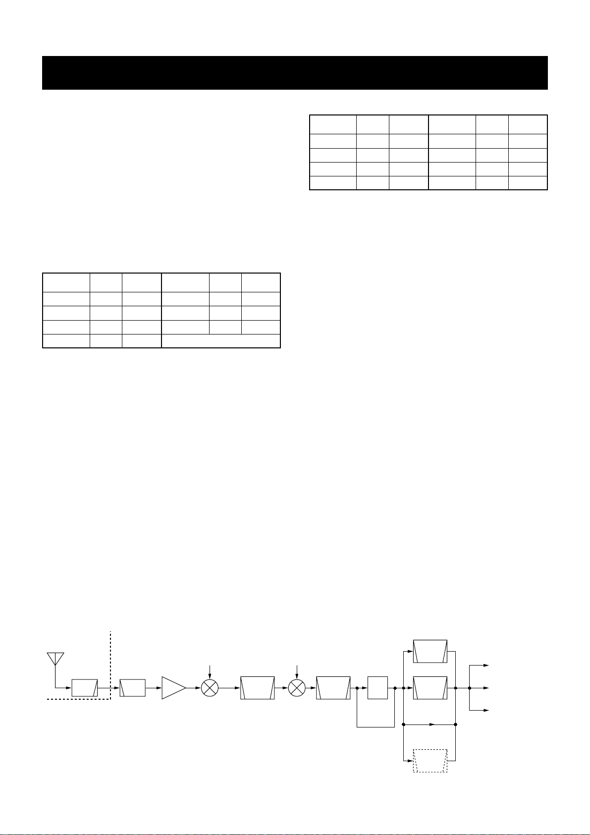
3-1 RECEIVER CIRCUITS
3-1-1 RF CIRCUIT (PA AND MAIN UNITS)
HF/50 MHz RF filters pass only the desired band signals
and suppress any undesired band signals. The HF/50 MHz
RF circuit has 7 low-pass filters and 6 high-pass filters for
specified band use.
HF/50 MHz RF signals from the [ANT] connector, pass
through one of 7 low-pass filters as below, the transmit/
receive switching relay (PA unit; RL250) and low-pass filter
(PA unit; L300, L301, C304–C308), and are then applied to
the MAIN unit via J300 (PA unit).
The signals from the PA unit are applied to or bypass the 20
dB attenuator (MAIN unit; R2, R3). The signals pass through
the high-pass filter (MAIN unit; L301–L303, C301–C303) to
suppress strong signals above 1.6 MHz and are then
applied to the HPF section.
(1) 0.03–2 MHz and 30–40 MHz
The signals pass through a low-pass filter (L304, L305,
C306–C310), and then applied to the preamplifier circuit on
the MAIN unit.
(2) 2–30 MHz
The signals from the low-pass filter (L304, L305,
C306–C310) are applied to one of 5 high-pass filters as at
right above and are then applied to the preamplifier circuit
on the MAIN unit.
(3) 40–60 MHz
The signals pass through the high-pass filter (L502–L504,
C501–C505) and the low-pass filter (L501, L506–L508
C506–C513), and are then applied to the preamplifier circuit
on the MAIN unit.
3-1-2 PREAMPLIFIER CIRCUIT (MAIN UNIT)
The preamplifier circuit in the IC-703 has approx. 15dB gain
over a wide-band frequency range.
When the preamplifier is turned ON, the signals from the RF
circuit are applied to the preamplifier (Q651) via D622 or
D632. Amplified or bypassed (passes through the D601 and
D602 when bypassed) signals are applied to the 1st mixer
circuit (D701).
3-1-3 1ST MIXER CIRCUIT (MAIN UNIT)
The 1st mixer circuit mixes the receive signals with the 1st
LO signal to convert the receive signal frequencies to a
64.455 MHz 1st IF signal.
The signals from the preamplifier circuit, or signals which
bypass the preamplifier, are passed through a low-pass filter (L681–L683, C681–C687) and then applied to the 1st
mixer (D701).
The 1st LO signal (one of the 64.485–124.455 MHz) is
amplified at Q751, filtered by a low-pass filter (L753,
C756–C759), passed through the attenuator (R771–R773),
and then applied to the 1st mixer.
3-1-4 1ST IF CIRCUIT (MAIN UNIT)
The 1st IF circuit filters and amplifies the 1st IF signals. The
1st IF signals are applied to a Crystal Filter (FI851) to suppress out-of-band signals.
The 64.445 MHz 1st IF signals pass through the crystal filter (FI851). Then the filtered signals are applied to the IF
amplifier (Q881).
The AGC voltage is supplied to the Q881’s gate to obtain
stable signal for AGC operation.
• Used RF high-pass filter (MAIN unit)
• Used RF low-pass filter (MAIN unit)
SECTION 3 CIRCUIT DESCRIPTION
Frequency
(MHz)
0.03–2 MHz
2–4 MHz
4–8 MHz
8–15 MHz
Frequency
(MHz)
15–22 MHz
22–30 MHz
30–60 MHz
Control
signal
F5
F6
F7
Control
signal
F1
F2
F3
F4
Entrance
coil
RL401
RL421
RL441
RL461
Entrance
coil
RL481
RL501
RL521
Frequency
(MHz)
0.03–2 MHz
2–4 MHz
4–8 MHz
8–15 MHz
Frequency
(MHz)
15–22 MHz
22–30 MHz
30–40 MHz
40–60 MHz
Control
signal
B5H
B6H
BTHH
B7RH
Control
signal
BTHH
B2H
B3H
B4H
Entrance
coil
D541
D551
D561
D571
Entrance
coil
D581
D591
D541
D501
• 2ND IF AND DEMODULATOR CIRCUIT
PA UNIT
[ANT]
0.03—60 MHz
LPFs
MAIN UNIT
HPFs
Pre-amp.
Q651
amp.
1st mixer
D701
1st LO:
69.0415 MHz—
530.0115 MHz
Crystal
64.455 MHz
FI851
filter
2nd LO:
60.0 MHz
2nd
mixer
D901
FI1501
Ceramic
filter
9.0115MHz
NB
Det.
FI1301
SSB, CW
filter
FI1341
AM, FM-N
filter
FM mode
Optional
filter
to AM demod.
circuit (D2001)
to BFO circuit
(IC1901)
to FM demod.
circuit (IC2101)
3 - 2
The amplified signals are then applied to the 2nd mixer circuit (D901).
3-1-5 2ND MIXER CIRCUIT (MAIN UNIT)
The 2nd mixer circuit mixes the 1st IF signals and 2nd LO
signal (64 MHz) to convert the 1st IF to a 2nd IF.
The 1st IF signals from the 1st amplifier (Q881) are converted to 455 kHz 2nd IF signals at the 2nd mixer circuit (D901).
The 2nd IF signals are applied to the bandpass filter
(FI1501) to suppress undesired signals, such as the 2nd LO
signal, and are then applied to the noise amplifier (Q1053).
3-1-6 NOISE BLANKER CIRCUIT (MAIN UNIT)
The noise blanker circuit detects pulse type noise, and turns
OFF the signal line when noise appears.
A portion of the signals from FI1501 are amplified at the
noise amplifiers (Q1051–Q1053), then detected at the noise
detector (D1002) to convert the noise components to DC
voltages.
The converted voltages are then applied to the noise
blanker gate (Q1002, Q1003, Q1402) by applying reversebiased voltage.
The detected voltage from Q1002 is also applied to the
noise blanker AGC circuit (Q1004, Q1005) and is then fed
back to the noise amplifier (Q1051–Q1053) as a bias voltage. The noise AGC circuit prevents closure of the noise
blanker gate for long periods by non-pulse-type noise.
The 2nd IF signals from the noise blanker gate are then
applied to the 2nd IF circuit.
3-1-7 2ND IF CIRCUIT (MAIN UNIT)
The 2nd IF circuit amplifies and filters the 2nd IF signals.
The 2nd IF signals from the ceramic bandpass filter (FI1501)
are amplified at the IF amplifier (IC1401) and applied to a
2nd IF filter as shown right column via the Tx/Rx switch
(D1402).
The filtered or bypassed signals are applied to the 2 amplifiers (Q1101, Q1201) and buffer amplifier (Q1251) to obtain
a detectable level at the demodulator circuit
The amplified signals from the buffer amplifier (Q1251) are
shared between the SSB/CW/RTTY detector (IC1901), AM
detector (D2001), FM detector (IC2101) and AGC detector
(D2501).
3-1-8 IF SHIFT CIRCUIT (MAIN UNIT)
The IF shift circuit shifts the center frequency of IF signals to
electronically shift the center frequency.
The IF shift circuit shifts the 1st LO and BFO within ±1.2 kHz
in SSB/CW/RTTY modes or ±250 Hz in CW-N/RTTY-N
modes. As a result, the 2nd IF (also 1st IF) is shifted from
the center frequency of the 2nd IF filter (FI1301, FI1341 or
optional IF filters). This means 2nd IF signals do not pass
through the center of the 2nd IF filter. Therefore, the higher
or lower frequency components of the IF are cut out. Since
the BFO frequency is also shifted the same value as the 1st
IF, frequency is corrected at the detector.
In the IC-703, the 1st LO frequency is shifted to change the
2nd IF because a fixed 2nd LO frequency (64 MHz) is used.
The 1st IF filter (FI1301) and 2nd IF filter (FI1501) have 15
kHz pass-band widths, and do not affect IF shift operation.
• Used 2nd IF filter
Mode Used filter Control signal
SSB, CW, RTTY
AM nar.
AM, FM nar.
FM
SSB nar.
CW nar., RTTY nar.
SSB wide
FL-65 (FI1301)
FL-94 (FI1341)
Bypassed
Optional FL-222
Optional FL-52A,
FL-53A
Optional FL-257
2F23
2F80
2FTH
2FOP
2FOP
2FOP
D1403
IC1401
Q1053
Q1401
NB DET.
2nd IF signal
to the detector circuits
"ALCL" signal
"AGC" signal
"T8V" signal
"NBS" signal
AGC
Amp.
IF
Q1052
Amp.
Q1051
D1002
Q1004
Q1005
Q1002
Q1003
Q1402
"NBLV" signal
Amp.
NB SWITCH
Q1001
Q1006
NB GATE
• NOISE BLANKER CIRCUIT

3 - 3
3-1-9 AGC CIRCUIT (MAIN UNIT)
The AGC (Automatic Gain Control) circuit reduces IF amplifier gain to keep the audio output at a constant level. The
receiver gain is determined by the voltage on the AGC line
(Q2503).
The 2nd IF signal from the buffer amplifier (Q1251) is detected at the AGC detector (D2501) and applied to the AGC
amplifier (Q2501). Q2501 sets the receiver gain with the
[RF/SQL] control via the “RFGV” signal line.
When receiving strong signals, the detected voltage increases and the AGC voltage decreases via the DC amplifier
(Q2503). The AGC voltage is used for IF amplifiers (Q881,
Q1401) to attenuate the received signals.
When AGC slow is selected, C2505 and R2506 are connected in parallel to obtain appropriate AGC characteristics.
The AGC signal is also applied to the meter amplifier
(IC2401), and is then applied to the main CPU (IC5901) to
use the S-meter as “SML” signal.
3-1-10 S-METER CIRCUIT (MAIN UNIT)
The S-meter circuit indicates the relative received signal
strength while receiving by utilizing the AGC voltage which
changes depending on the received signal strength.
The output voltage of the meter amplifier (IC2401, pin 7) is
applied to the main CPU (IC5901) as an S-meter signal via
the A/D converter (IC5601) as the “SML” signal.
The S-meter signal from the main CPU (IC5901) is applied
to the sub CPU, and is then displayed on the S-meter readout.
3-1-11 SQUELCH CIRCUIT (MAIN UNIT)
The squelch circuit mutes audio output when the S-meter
signal is lower than the [RF/SQL] control setting level.
In SSB/CW/RTTY modes, the S-meter signal is applied to
the main CPU (IC5901, pin 36) and is compared with the
threshold level set by the [RF/SQL] control. The [RF/SQL]
setting is picked up at the sub CPU (DISPLAY board; IC6,
pin 97). The main CPU compares the S-meter signal and
[RF/SQL] setting, and controls the AF selector switch
(IC2301) to cut out AF signals.
In FM mode, a portion of the AF signals from the FM IF IC
(IC2101, pin 9) are applied to the active filter section (pin 8)
where noise components above 20 kHz are amplified. The
signals are rectified at the noise detector section and then
output from pin 14. The noise squelch signal from pin 14 is
applied to the main CPU (IC5901, pin 31) via the A/D converter (IC5601, pin 11) as the “NSQL” signal. The CPU then
controls the AF selector switch (IC2301).
3-1-12 DEMODULATOR CIRCUITS (MAIN UNIT)
(1) SSB/CW/RTTY modes
The 2nd IF signals from the buffer amplifier (Q1251) are
mixed with the BFO signal from the PLL circuit at the SSB
detector (IC1901, pins 3, 6). The detected AF signals from
IC1901 (pin 1) are applied to the AF selector switch (IC2301,
pin 12) via the “SSAF” signal.
(2) AM mode
The 2nd IF signals from the buffer amplifier (Q1251) are
detected at the AM detector (D2001). The detected AF signal is applied to the AF selector switch (IC2301, pin 12) via
the “AMAF” signal.
(3) FM/FM NARROW modes
The 2nd IF signals from the buffer amplifier (Q1251) are
applied to the FM IF IC (IC2101, pin 5) where the IF signals
are converted into 455 kHz IF signals. The signals are
applied to the quadrature detector section. X2101 is used for
quadrature detector. The detected AF signals from pin 9
pass through the de-emphasis circuit (IC2401), and are then
applied to the AF selector switch (IC2301, pin 14) via the
“FMAF” signal.
• AGC CIRCUIT
RFGV
(RF gain control)
2nd IF
signal
C2501
8 V
R2507
AGC det.
D2502
R2508
D2501
C2502
R2502
Q2501
R2504
C2503
R2503
R2505
C2504
Q2502
R2506
C2505
Q2503
IC2401
Amp.
SML
S-meter signal

3 - 4
3-1-13 AF SELECTOR SWITCH (MAIN UNIT)
The AF signals from one of the detector circuits are applied
to the AF selector switch (IC2301). IC2301 consists of dual
3-channel analog switches which are selected with a mode
signal and the squelch control signal.
3-1-14 AF AMPLIFIER CIRCUIT (MAIN UNIT)
The AF amplifier amplifies the demodulated signal to a suitable driving level for the speaker.
The AF signals from the AF selector switch (MAIN unit;
IC2301) pass through the 3 kHz low-pass filter (IC2401),
and are then applied to the DSP switch (IC2461, pin 6)
which mute the beep sound when DSP unit’s power ON or
OFF.
The AF signals are applied to the VCA (Voltage Controlled
Amplifier) circuit (IC7201). The AF gain setting from the main
CPU is converted to DC voltage at the D/A converter
(IC6501) and applied to the VCA control terminal (IC7201)
via the “AFGV” signal line.
The CW side tone/beep tone (“BEEP” signal from the buffer
amplifier IC7001, pin 8) and optional synthesized voice
(“SPCH” signal from the UT102) are also applied to the VCA
circuit.
The output AF signals from IC7201 (pin 9) are power-amplified at IC7301 to drive the speaker, and are then applied to
the speaker (CHASSIS unit; SP1) via J7372.
3-2 TRANSMITTER CIRCUITS
3-2-1 MICROPHONE AMPLIFIER CIRCUIT
(MAIN UNIT)
The microphone amplifier circuit amplifies microphone input
signals and outputs the amplified signals to the balanced
modulator or FM modulation circuit.
Audio signals from the front or rear panel [MIC] connector
enter the microphone amplifier IC (IC1621, pin 12) and are
then amplified at the microphone amplifier or speech compressor section via the R1621.
The amplified or compressed signals are applied to the VCA
section of IC1601. The microphone gain setting from the D/A
converter (IC6501, pin 11) is applied to the VCA control terminal (IC1601, pin 8). The resulting signals from pin 9 are
then applied to the buffer amplifier (Q1721) via the analog
switch (IC1701). External modulation input from the [ACC]
socket (J6951, pin 11) is also applied to Q1721.
While in SSB mode, the amplified signals from the buffer
amplifier (Q1721) are passed through the AF selector switch
(IC1751) and are then applied to the balanced modulator
(IC1801).
While in AM/FM mode, the amplified signals from the buffer
amplifier (Q1721) are applied to the IDC amplifier (IC2201).
The signals are then applied to the AF selector switch
(IC1751) via the AM depth controller (R2618) in AM mode or
to the varactor diode (D9622) via the FM max deviation controller (R2621) and AF selector switch (IC2651) in FM mode.
3-2-2 VOX CIRCUIT (MAIN UNIT)
The VOX (Voice-Operated-Transmission) circuit sets transmitting conditions according to voice input.
When the VOX function is activated, the microphone signals
are amplified at microphone amplifier (IC1621, pin 10), and
are then applied to the VOX comparator section in the main
CPU (IC5901, pin 93) via the “VOXL” line.
A portion of the power amplified AF signals from the AF
power amplifier (IC7301) are amplified at the buffer amplifier (IC7001, pin 13) and applied to the anti-VOX comparator
section in the main CPU (IC5901, pin 92) via the “AVXL”
line.
Then the main CPU compares these and controls the transmitter circuit.
3-2-3 BALANCED MODULATOR (MAIN UNIT)
The balanced modulator converts the AF signals from the
microphone amplifier to a 9 MHz IF signal with a BFO (Beat
Frequency Oscillator) signal.
Microphone signals from the AF selector switch (IC1751) are
applied to the balanced modulator (IC1801, pin 3). The BFO
signal is applied to IC1801 (pin 1) as a carrier signal.
e
• AF SELECTOR SWITCH
• MICROPHONE AMPLIFIER CIRCUIT
IC2301
SSB/CW/
RTTY
AM
FM
12
X0
15
X2
14
X1
13
X
AF signal
to the AF amplifi
INH
6
AFS1, AFS2
SQL
9, 10
IC1621
AF signals from
the microphone
"VOXL" signal
12
10
Amp.
Comp.
Amp.
14
7
8
"COMS" signal
IC1601
VCA
IC1602
"VOXL" signal
IC1701
SW
to the modulation circuit

3 - 5
IC1801 is a double balanced mixer IC and outputs a double
side band (DSB) signal with –40 dB of carrier suppression.
R1803 and R1807 adjust the balanced level of IC1801 for
maximum carrier suppression. The resulting signal passes
through a 9 MHz IF filter (FI1301 in SSB/CW/RTTY modes)
to suppress unwanted side-band signals.
In AM mode, R1811 is connected to upset the balance of
IC1801 via Q1803 for leaking the BFO signal as a carrier
signal. The CW keying/RTTY TX signal is applied to IC1801
pin 3.
3-2-4 FM MODULATION CIRCUIT (MAIN UNIT)
The microphone signals from Q1721 are applied to the IDC
amplifier (IC2201, pin 5). The sub-audible tone signal
(67.0–254.1 Hz) from the main CPU (IC5901, pin 2) is also
applied to the same amplifier (IC2201, pin 2) for repeater
use.
The resulting signals are applied to the VCO circuit (Q9621,
D9621) via IC2651 to change the reactance of the varactor
diode (D9622) for FM modulation. The modulated signal is
amplified at the buffer amplifier (Q9651).
3-2-5 TRANSMITTER IF CIRCUIT (MAIN UNIT)
The 9 MHz IF signal from the modulation circuit passes
through the 9 MHz IF filter (FI1301 in SSB/CW/RTTY
modes; FI1341 in AM/FM-N modes; through in FM mode).
The signal is amplified at Q1401, and then passes through
the crystal filter (FI1501). The signal is then applied to the
2nd mixer (D901).
The signal is mixed with the 2nd LO signal (60 MHz) and
converted to a 69 MHz IF signal at the 2nd mixer (D901).
The 69 MHz IF signal passes through a bandpass
filter(FI851), IF amplifier (Q831), and is then converted to
the displayed frequency at the 1st mixer (D701) with the 1st
LO signal. The mixers (D701) and bandpass filter (FI851)
are used commonly for both receiving and transmitting.
3-2-6 RF CIRCUIT (MAIN AND PA UNITS)
The RF circuit amplifies the displayed frequency signal to
obtain 10 W of RF output power for HF/50 MHz bands.
The HF/50 MHz RF signals from the 1st mixer (D701) via the
low-pass filter pass through one of 8 high-pass filters (Refer
to page 3-1 for used RF high-pass filter). The 50 MHz RF
signals pass through a low-pass filter additionally. The filtered signals pass through the low-pass filter (except 50
MHz), are then amplified at the YGR amplifier (IC101) after
being passed through the high-pass filter to cut the unwanted signal below 1.6 MHz, and are then applied to the PA
unit.
The signals from IC101 enter the PA unit and is amplified at
the pre drive and power amplifiers (Q101, Q150, Q200 and
Q201) to obtain a stable 10 W of RF output power in
sequence. The amplified signals are applied to the band
switch (RL250).
The power-amplified signals from the band switch (RL250)
are then applied to the [ANT] connector via one of the 7 lowpass filters.
3-2-7 ALC CIRCUIT (PA AND MAIN UNITS)
The ALC (Automatic Level Control) circuit reduces the gain
of IF amplifiers in order for the transceiver to output a constant RF power set by the RF power setting even when the
supplied voltage shifts, etc.
The HF/50 MHz RF power signal level is detected at the
power detector (D562, D563), buffer-amplified at IC560 and
applied to the MAIN unit as the “FORL” voltage.
The “FORL” voltage is applied to the ALC amplifier (MAIN
unit; IC2701, pin 2). The “POCV” voltage from the D/A converter (MAIN unit; IC6501, pin 23), determined by the RF
power setting, is applied to the same amplifier (MAIN unit;
IC2701, pin 3) as the reference voltage.
2nd
mixer
1st
mixer
FM tone
D901
D701
Q9621
D9621
IC1621
IC2201
Crystal
filter
FI671, FI681,
or optional filter
MIC
FI854
Crystal
filter
BPFs
LPF
Amp.
IC1621
IF
Q1401 FI501
Amp.
Q9651
Amp.
IDC
FM, AM
AM
FM
SSB
BPF
HPF
HPF
HPF
50 MHz
¥
¥
¥
LPF
LPF
LPF
¥
¥
¥
IC101
YGR
Q501
Antenna
Pre.
Q150
Drive
Q200,
Q201
Power
LPF LPF
• TRANSMITTER CONSTRUCTION

3 - 6
When the “FORL” voltage exceeds the “POCV” voltage, ALC
bias voltage from IC2701 (pin 1) controls 1st and 2nd IF
amplifiers (Q831, Q1401). This adjusts the output power to
the level determined by the RF power setting until the
“FORL” and “POCV” voltages are equalized.
In AM mode, IC2701 operates as an averaging ALC amplifier with Q2703. Q2703 turns ON and the “POCV” voltage is
shifted for 4 W AM output power.
The ALC bias voltage from IC2701 is also applied to the
main CPU (IC5901) via the A/D converter (IC5601) as the
“ALCL” voltage for ALC meter indication.
An external ALC input (minus voltage) from the [ACC] socket (pin 6) is shifted to plus voltage at D2781 and is applied
to the buffer amplifier (Q2781). External ALC operation is
identical to that of the internal ALC.
3-2-8 APC CIRCUIT (MAIN UNIT)
The APC (Automatic Power Control) circuit protects the
power amplifiers on the PA unit from high SWR and excessive current for the HF/50 MHz band.
The reflected wave signal appears and increases on the
antenna connector when the antenna is mismatched. The
HF/50 MHz reflected signal level is detected at D561 (PA
unit), and is amplified at the APC amplifier (IC2701) and
applied to the ALC circuit as the reference voltage.
For the current APC, the driving current at the power amplifier is detected in the voltages (“IDH” and “IDL”) which
appear at both terminals of a 0.012 Ω resistor (R216) on the
PA unit. The detected voltages are applied to the differential
amplifier (IC2701, pins 9, 10). When the current of the power
amplifier exceeds allowed current, IC2701 controls the ALC
line via IC2701 to prevent excessive current flow.
3-2-9 RF, ALC, SWR METER CIRCUITS
(MAIN UNIT)
While transmitting, RF, ALC or SWR meter readings are
available and can be selected with the [MET] switch.
(1) Power meter
The “FORL” voltage is applied to the main CPU (IC5901) via
the A/D converter (IC5601, pin 12) for indicating the output
power.
• FREQUENCY CONSTRUCTION
(0.03—60 MHz)
Antenna
1st IF signal
(64.455 MHz)
1st mixer
D701
1st LO signal
(64.4850—124.4550 MHz)
ATT3 dB
LPF
Ref Oscillator
X9501
Q811 Q881
IF
1
*
Oscillates 64.4850—94.454999 MHz
2
*
Oscillates 94.4550—124.454999 MHz
LO
Q751
69.0115 MHz
(WFM: 70.7 MHz)
Crystal
BPF
HPF LPF
Amp.
IC9521 IC9001 IC9101
DDS
2nd IF signal
(455 kHz)
2nd mixer
D901
IF
2nd LO signal
(64.0 MHz)
1
*
( for HF bands)
Amp.
Q9301
2
*
( for 50 MHz band)
PLL IC
to each detector circuits
Q9201
D9201
Q9621
D9621
MAIN LOOP CIRCUIT
PLL IC
IC9601
Q9621
D9621
(Oscillates 64.0 MHz)
SINGLE LOOP CIRCUIT
Amp.
Q9651
LPF
ATT
3 dB

3 - 7
(2) ALC meter
The ALC bias voltage from IC2701 pin 14 is applied to the
main CPU (IC5901) via the “ALCV” signal line for indicating
the ALC level.
(3) SWR meter
The “FORL” and “REFL” voltages are applied to the main
CPU (IC5901) via the A/D converter (IC5601, pins 12 and 1)
respectively. The main CPU compares the ratio of “FORV” to
“REFV” voltage and indicates the SWR for the [ANT] connector.
3-3 PLL CIRCUITS
3-3-1 GENERAL
The PLL circuits generates a 1st LO frequency
(64.485–124.455 MHz), a 2nd LO frequency (64 MHz), a
BFO frequency (455 kHz).
The 1st LO PLL circuit adopts a mixer-less dual loop PLL
system and has 2 VCO circuits. The BFO uses a DDS and
the 2nd LO uses a 64 MHz fixed frequency.
3-3-2 1ST LO PLL CIRCUIT (MAIN UNIT)
The 1st LO PLL contains a main loop and reference loop
forming a dual loop system.
The reference loop generates a 6.5 MHz frequency using a
DDS circuit, and the main loop generates a 64.485 to
124.455 MHz frequency using the reference loop frequency.
(1) REFERENCE LOOP PLL
The oscillated signal at the reference passes through the
low-pass filter (L9521, L9523, C9521–C9526), and is then
amplified at the amplifier (IC9521). The amplified signal is
applied to the DDS IC (IC9001, pin 5) via the low-pass filters
(L9524, L9525, C9528–C9530, L9021, L9022,
C9023–C9025). The signal is then divided and detected on
phase with the DDS generated frequency.
The detected signals output from IC9001 (pin 10) are amplified at the buffer amplifier (Q9051), and then pass through
the band-pass filter (L9051–L9053, C9053–C9056) to suppress spurious components. The signal is applied to the PLL
IC (IC9101, pin 1) as PLL lock voltage.
(2) MAIN LOOP PLL
The oscillated signal at one of the main loop VCOs (HF:
Q9201, 50 MHz: Q9251) is amplified at the buffer amplifier
(Q9301) and is then applied to the PLL IC (IC9101, pin 4).
The signal is then divided and detected on phase with the
reference loop output frequency.
The detected signal output from the PLL IC (IC9101, pin 13)
is converted into a DC voltage (lock voltage) at the active
loop filter and then fed back to one of the varactor diodes
(D9201, D9251) in the VCO circuits
The oscillated signal passes through a low-pass and highpass filters, and is then applied to the 1st mixer (D701) as a
1st LO signal.
3-3-3 2ND LO AND REFERENCE OSCILLATOR
CIRCUITS (MAIN UNIT)
The reference oscillator (IC9601, Q9621, X9501) generates
a 64 MHz frequency used for the 2nd LO signal.
The oscillated signal is amplified at the buffer amplifier
(Q9651), and is then passed through the low-pass filter
(L9672, C9673, C9675) to suppress the high harmonics
components. The filtered 64 MHz signal is applied to the 2nd
mixer (D901) via the 3 dB attenuator (R9672–R9674) as a
2nd LO signal.
3-3-4 BFO CIRCUIT (MAIN UNIT)
The DDS IC (IC9701) generates a 455 kHz BFO signal. The
signa is passed through the low-pass filter (L9751, C9753,
C9754, C9756) to suppress high harmonics suprious components. The 455 kHz BFO signal is then applied to the SSB
detector (IC1901, pin 3) and SSB modulator (IC1801, pin 1)
via the “BFO” signal line.
While transmitting in RTTY mode, the RTTY keying signal is
applied to IC9701 to shift the generated frequency and to
obtain 2 frequencies for FSK operation.
CW receiving pitch control, RTTY receiving tone, RTTY
transmitting mark are controled by changing BFO frequency.
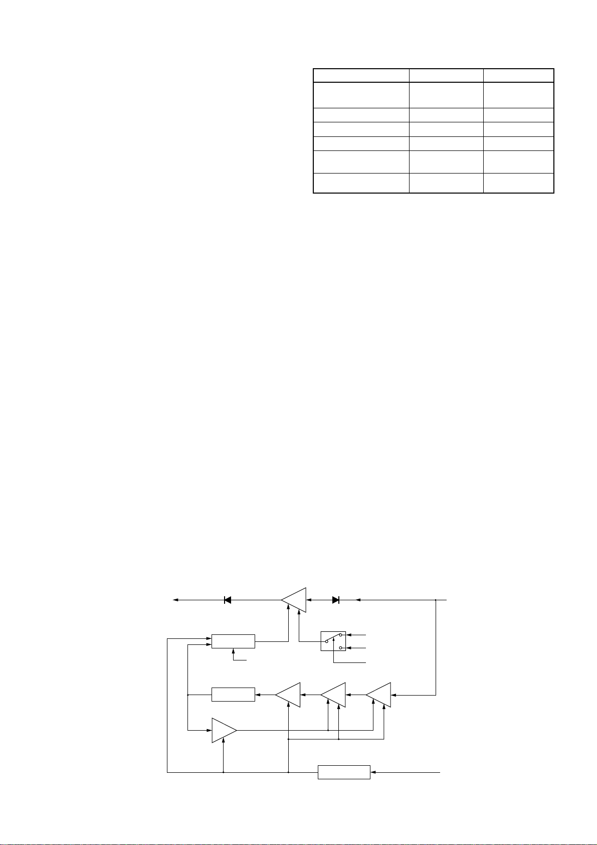
3-4 ANTENNA TUNER CIRCUITS
3-4-1 ANTENNA MATCHING NETWORK CIRCUIT
(PA UNIT)
The antenna tuner circuit consists of the antenna matching
network circuit, SWR detector circuit, impedance detector
circuit, phase detector circuit, etc.
When antenna tuning is ON, the antenna matching network
circuit switches ON via the RL640 and RL641.
The attenuator’s impedance is set to 50 Ω which is same as
power amplifier’s output impedance. The attenuator’s input
impedance is about SWR 1, however its output impedance
changes variably. Therefore, attenuator’s output impedance
is matched to the antenna to become about SWR 1, then
impedance matching is depended on input impedance. The
antenna matching network circuit switches OFF via the
RL640 and RL641 when the impedance is matched between
the output impedance and antenna.
The antenna matching network circuit is composed between
RL640 and RL641. Therefore, each detecting circuits work
when antenna tuning is ON only. Thus, There isn’t influence
about loss of each detecting circuits when antenna tuning is
OFF. In addition, the output power from the power amplifier
(Q200, Q201) is applied to the this circuit as low power via
the attenuator. Therefore, the output power doesn’t effect to
interference while impedance tuning.

3 - 8
3-4-2 OUTPUT POWER DETECTING CIRCUIT
(PA UNIT)
The output power from the power amplifier (Q200, Q201) is
divided at the C640 and C641. The divided voltage is
applied to the power detecting circuit (D640) as detecting
voltage. The detected voltage is applied to the main CPU
(MAIN unit; IC5901) via the A/D convertor (MAIN unit;
IC5601) as “TPZL” signal after being passed through the
switch circuit (IC641, Q646).
3-4-3 IMPEDANCE DETECTING CIRCUIT
(PA UNIT)
The output power from the power amplifier (Q200, Q201) is
applied to the RL640. The signal is applied to the power
detector (D640), and is then applied to the main CPU (MAIN
unit; IC5901) as the reference voltage. The voltage is also
used for power detecting voltage when the antenna tuning is
ON.
The attenuator’s output voltage is depended on the condition between power amplifier’s output impedance and the
antenna (For example, the voltage becomes high when the
impedance is high, the votage becomes low when the
impedance is low). The voltage is amplified at the Q641, and
is then detected at the impedance detector (D646). The signal is applied to the main CPU (MAIN unit; IC5901) to analyze whether the impedance is more than 1.1 or not.
3-4-4 PHASE DETECTING CIRCUIT (PA UNIT)
The phase detecting circuit is composed D643, L640 and
L641.
The input side signal passes through the C646 to shift the its
phase for +90 degrees. The signal is applied to the phase
detecting circuit (L640).
The output side signal is applied to the amplifiers (Q643,
Q811). The amplified signal is applied to the phase detecting circuit (L641).
The detected signal is applied to the comparator circuit
(IC640, pin 2), and is then applied to the main CPU (MAIN
unit; IC5901, pin 75) via the “TPHK” signal.
3-4-5 SWR DETECTING CIRCUIT (PA UNIT)
The SWR detecting circuit employs return loss bridge circuit
(L642, R662–R665) which is also composed as 6 dB attenuator (input-output impedance is 50 Ω).
The output power from the power amplifier (Q200, Q201)
passes through the attenuator, and is then applied to the
SWR detecting circuit (D645). The signal is applied to the
main CPU (MAIN unit; IC5901) via the A/D convertor (MAIN
unit; IC5601) as “TSWL” signal.
The main CPU is analyzed SWR to use the “TSWL” signal
from the SWL detecting circuit and “TPZL” signal from the
power detecting circuit.
• ANTENNA TUNER CONSTRUCTION
"TDTS" signal from the
main CPU
(MAIN unit; IC5901, pin 44)
The signal from the
power/SWR detector
(D560, D561)
RL640 RL641
ATT
"TPZL" signal to the A/D
convertor
(MAIN unit; IC5601, pin 15)
"TPZS" signal to the main
CPU
(MAIN unit; IC5901, pin 74)
IC641
Q646
Switch
D646
Impedance
detector
D643
Phase
detector
D640
Power
detector
D645
SWR
detector
Q641
Amp.
Q643
Q811
Amp.
IC640
Comparator
to the antena
"TSWL" signal to the A/D
convertor
(MAIN unit; IC5601, pin 2)
"TPHK" signal to the main
CPU
(MAIN unit; IC5901, pin 75)

3 - 9
Description
Common 3 V converted from the HV line by the
+3 regulator circuit (IC9901).
Common 3 V converted from the 14V line by the
+3 regulator circuit (IC9921).
Common 5 V converted from the 14V line by the
+5 regulator circuit (IC9941).
The same voltage as the 5V line which is controlled by the switching circuit (Q9964, Q9966).
The circuit is controlled by the “PSS” signal from
the CPU (IC5901, pin 90).
Common 8 V converted from the 14V line by the
+8 regulator circuit (IC9961).
The same voltage as the 8V line which is controlled by the switching circuit (Q9963, Q9965).
The circuit is controlled by the “PSS” signal from
the CPU (IC5901, pin 90).
Receive 8 V which is the same voltage as the 8V
line controlled by the switching circuit (Q6322,
Q6323) using the “RXS” signal from the CPU
(IC5901, pin 36).
Transmit 8 V which is the same voltage as the 8V
line controlled by the switching circuit (Q6342,
Q6343) using the “TXS” signal from the CPU
(IC5901, pin 35).
Line
H3V
3V
5V
P5V
8V
P8V
R8V
T8V
3-5 POWER SUPPLY CIRCUITS
3-5-1 VOLTAGE LINES (MAIN UNIT)
Description
The voltage from a DC power supply.
The same voltage as the HV line which is controlled by the power switching circuit (Q80, Q81).
When the [POWER] switch is pushed, the CPU
outputs the “POWS” control signal to the power
switching circuit to turn the circuit ON.
Line
HV
14V
3-5-2 PA UNIT VOLTAGE LINES
Description
Common 8 V line from the +8 regulator circuit
(MAIN unit; IC9961). The voltage is applied to the
microphone via the J1, pin 1.
Common 5 V converted from the 5V line by the
+5 regulator circuit (IC5, Q10, Q11, D9). The output voltage is applied to the SUB-CPU (IC6),
LCD driver (IC2), etc.
Line
8V
5V
3-5-3 VOLTAGE LINES (DISPLAY BOARD)
1
2
3
4
5
8
9
16
18
19
20
21
22
23
25
26
27
28
31
33
34
39
Outputs beep audio and CW side tone
signals.
Outputs CTCSS tone signal.
Outputs the serial data to the PLL IC
(IC9601).
Input port for transmitting signals from
the microphone or ACC connector.
Outputs the serial clock to the PLL IC
(IC9601).
Outputs control signal for the optional
2nd IF filter.
High : While the filter is selected.
Outputs control signal for the 2nd IF filter.
High : While the filter is bypassed.
Input port for the shock detecting signal.
Input port for the [POWER] swtich on
the front panel.
Low : While the [POWER] is
pushed.
Outputs control signal for the 2nd IF filter.
High : While the 8 kHz filter is ON.
Outputs control signal for the 2nd IF filter.
High : While the 2.3 kHz filter is ON.
Input port for the PLL unlock signal.
Low : While the PLL is unlocked.
Outputs tuner data signal.
Outputs CW key down signal.
High : While transmitting on CW or
RTTY modes.
Output SSB modulation prohibitive signal.
High : While transmitting on CW, FM
or RTTY modes.
Input port for the PTT signal from the
data terminal (J6851, pin 3).
High : While data are transmitting.
Input port for the data signal from the
front unit.
Outputs data signal to the front unit.
Outputs LO level control signal.
Outputs CI-V signals.
Input port for the CI-V signals.
Outputs strobe signal to the PLL IC
(IC9601) for the 2nd LO signal.
3-6 CPU PORT ALLOCATIONS
3-6-1 MAIN CPU PORT ALLOCATIONS
(MAIN UNIT; IC5901)
BEEP
TONE
PDT
SNDK
PCK
2NOP
2NTH
TGK
PWRK
2N80
2N23
UNLK
TDAT
KDS
MINH
DPTK
LRXD
LTXD
SLOS
CTXD
CRXD
P2ST
Pin Port
Description
number name

3 - 10
40
41
42
43
46
47
49
50
51
52
53
55
56
57
58
59
61
65
66
67
72
73
80
Outputs strobe signal to the BFO’s
DDS IC (IC9701).
Outputs strobe signal to the DDS IC
(IC9001) for main loop.
Outputs strobe signal to the PLL IC
(IC9101) for main loop.
Outputs strobe signal to the D/A convertor (IC6501).
Input port for the RTTY keying signal.
High : While marking.
Low : While spacing.
Outputs AGC first control signal.
Low : While AGC first is ON.
Outputs FM mode select signal.
High : While FM or FM-N is selected.
Outputs AM mode select signal.
High : While AM or AM-N is selected.
Outputs noise blanker control signal.
High : While noise blanker is ON.
Outputs detecting output select signal.
High : While AM or AM-N is selected.
Outputs detecting output select signal.
High : While FM or FM-N is selected.
Outputs attenuator control signal.
High : While attenuator is ON.
Outputs the pre-amplifier ON/OFF
control signal.
High : While the pre-amplifier is OFF.
Outputs the pre-amplifier ON/OFF
control signal.
High : While the pre-amplifier is ON.
Outputs the speech compressor control signal.
High : While the speech compressor
is ON.
Outputs 9600 bps packet mode control
signal.
High : While 9600bps packet mode
is ON.
Outputs optional DSP unit control signal.
High : While the DSP unit is ON.
Outputs the EEPROM clock signal.
I/O port for the EEPROM data signal.
Outputs reset signal.
Input port for the external paddle dash
signal.
Input port for the external paddle dot
signal.
Outputs AF mute control signal.
Low : While AF is muting.
SBST
PDST
PMST
DSTB
FSKK
AGFS
FMS
ANS
NBS
AFS2
AFS1
ATTS
PROS
PRES
COMS
D96S
DSPS
ECK
EDT
DRES
DASK
DOTK
AFMS
(MAIN unit; IC5901)–Continued
Pin Port
Description
number name
85
89
90
91
95
98
99
100
Outputs the speaker switching signal.
High : The speaker is ON.
Input port for supplied voltage detecting signal.
Outputs power save control signal.
Low : While power save is ON.
Input port for the microphone
[UP]/[DWON] signal from the rear
panel.
Input port for the CTCSS signal.
Outputs strobe signal to the expander
IC (IC6101, pin 1).
Outputs serial data to the D/A convertor (IC6501, pin 8) and expander IC
(PA unit; IC600, pin 8).
Outputs serial clock to the D/A convertor (IC6501, pin 7) and expander IC
(PA unit; IC600, pin 7).
SPS
VCCL
PSS
MUDL
CTCL
MSTB
MDT
MCK
Pin Port
Description
number name
(MAIN unit; IC5901)–Continued

3 - 11
85
86
88
89
90
91
92
93
94
95
96
97
99
Outputs the communicating signal with
the main unit.
Input port for the sub-dial’s B phase
signal.
Input port for [P.AMP/ATT] and
[TUNER/CALL] keys.
Input port for [MENU] and [F-1] keys.
Input port for [F-2] and [F-3] keys.
Input port for [DISPLAY] and [LOCK]
keys.
Input port for [MODE] and [TS] keys.
Input port for [BAND UP] and
[BAND DN] keys.
Input port for the microphone PTT signal.
Input port for the microphone
UP/DOWN signal.
Input port for the AF volume control
signal.
Input port for the RS/SQL volume control signal.
input port for the SHIFT volume control
signal.
LTXD
SDBK
PRAK/
TUNK
MENK/
F1K
F2K/F3K
DISK/
LCKK
MODK/
TSK
BUPK/
BDNK
PTTL
FUDL
AFGL
SQLL
SFTL
(DISPLAY BOARD; IC6)–Continued
Pin Port
Description
number name
2
3
4
5
6
7
8
16
17
18
19
20
21
22
24
25
26
29
30
31
39–42
44–50
51–82
83
84
Output key backlight control signals.
Input port for the phone plug insert
detecting signal.
High : While the phone plug is insert-
ed.
Input port for the [RIT/SUB] key.
Input port for the main dial’s A phase
signal.
Input port for the main dial’s B phase
signal.
Input port for the sub dial’s A phase
signal.
Outputs the “P.AMP” LED control signal.
Outputs the “ATT ” LED control signal.
Outputs the “TUNER” LED control signal.
Outputs the “RIT” LED control signal.
Outputs the “LOCK” LED control signal.
Outputs the “RX” LED control signal.
Outputs the “TX” LED control signal.
Output the LCD backlight control signals.
Outputs sub-dial’s LED control signal.
Output the LCD driver (IC2) control
signals.
Output LCD common signals.
I/O port for LCD driver’s data signals.
Output LCD segment signals.
Outputs the LCD driver reset signal.
Low : While the LCD driver is reset.
Input port for the communicating signal with the main unit.
3-6-2 SUB CPU PORT ALLOCATIONS
(DISPLAY BOARD; IC6)
KL1S
KL2S
PHNK
RSK
MDAK
MDBK
SDAK
PRED
ATTD
TUND
RITD
LCKD
RXD
TXD
BL1S
BL2S
SUBD
WR
RD
A0
COM4–
COM1
DB7–
DB0
SEG1–
SEG32
LRES
LRXD
Pin Port
Description
number name
KL1S KL2S Lights
Low Low OFF
High Low Low
High High High
BL1S BL2S Lights
Low Low OFF
High Low Low
High High High

4 - 1
4-1 PREPARATION BEFORE SERVICING
■ REQUIRED TEST EQUIPMENT
DC power supply
RF power meter
(terminated type)
Frequency counter
RF voltmeter
Standard signal
generator (SSG)
FM deviation meter
Modulation analyzer
Distortion meter
Oscilloscope
Digital multimeter
AC millivoltmeter
DC voltmeter
DC ammeter
Audio generator
Spectram analyzer
Attenuator
External speaker
EQUIPMENT GREDE AND RANGE EQUIPMENT GREDE AND RENGE
SECTION 4 ADJUSTMENT PROCEDURES
Output voltage : 13.8 V DC
Current capacity : 5 A or more
Measuring range : 0.1–50 W
Frequency range : 1.8–100 MHz
Impedance : 50 Ω
SWR : Less than 1.2 : 1
Frequency range : 0.1–100 MHz
Frequency accuracy : ±1 ppm or better
Sensitivity : 100 mV or better
Frequency range : 0.1–100 MHz
Measuring range : 0.01–10 V
Frequency range : 0.1–100 MHz
Output level : 0.1 µV–32 mV
(–127 to –17 dBm)
Frequency range : 0–100 MHz
Measuring range : 0 to ±5 kHz
Frequency range : At least 100 MHz
Measuring range : 0–100 %
Frequency range : 1 kHz ±10 %
Measuring range : 1–100 %
Frequency range : DC–100 MHz
Measuring range : 0.01–10 V
Imput impeadance : 10 MΩ/DC or beter
Measuring range : 10 mV–10 V
Input impedance :
50 kΩ/V DC or better
Measurement capability: 1 A/50 A
Frequency range : 300–3000 Hz
Measuring range : 1–500 mV
Frequency range : At least 1000 MHz
Spectraum bandwidth : 100 kHz or more
Power attenuation : 50 or 60 dB
Capacity : 150 W or more
Input impedance : 8 Ω
Capacity : 5 W or more
‘‘
CONNECTIONS
Microphone connector
¥ (Rear panel view)
Pin 5
MIC GND
Pin 6
MIC INPUT
18
DC power supply
AA13.8 V/3 A
Keyer
Pin 7
GND
—
+
generator
Pin 4
PTT
AM meter
1 A, 10 A
Audio
to [MIC]
to [DC 13.8 V]
to [ELEC KEY]
to [EXT SP]
to [ANT]
AC
millivoltmeter
Speaker
Attenuator
50 or 60 dB
RF power meter
A200 W/50
Standard signal
aagenerator
Spectrum
analyzer
FM deviation
AAmeter
Modulation
aanalyzer
Frequency counter
i703
CAUTION:
DO NOT connect the
standard signal generator
while transmitting.

4 - 2
4-2 PLL ADJUSTMENTS
REFERENCE
FREQUENCY
VCO1 LOCK
VOLTAGE
VCO2 LOCK
VOLTAGE
ADJUSTMENT
ADJUSTMENT ADJUSTMENT CONDITION
MEASUREMENT
VALUE
POINT
UNIT LOCATION UNIT ADJUST
1
2
1
1
• Display frequency: Any
• Receiving
• Display frequency: 29.99999 MHz
• Mode : USB
• Receiving
• Display frequency
: 60.00000 MHz
• Mode : USB
• Receiving
MAIN
MAIN
MAIN
Connect an RF voltmeter to check point
CP9611.
Connect a frequency
counter to check
point CP9671.
Connect a digital
multimeter or oscilloscope to check point
CP9151.
Connect a digital
multimeter or oscilloscope to check point
CP9151.
1.5–3.5 V
64.000000 MHz
4.0 V
4.0 V
MAIN
MAIN
MAIN
Verify
R9552
C9202
C9252

4 - 3
• MAIN UNIT TOP VIEW
CP9671
CP9611
Reference frequency
check point
R9552
Reference frequency
adjustment
C9202
VCO1 lock voltage
adjustment
C9252
VCO2 lock voltage
adjustment
CP9151
VCO1 and VCO2
lock voltage check point

4 - 4
4-3 TRANSMITTER ADJUSTMENTS
TRANSMIT
PEAK
POWER
CARRIER
SUPPRESSION
TRANSMIT
TOTAL GAIN
OUTPUT
POWER
Id APC
ADJUSTMENT
ADJUSTMENT ADJUSTMENT CONDITION
MEASUREMENT
VALUE
POINT
UNIT LOCATION UNIT ADJUST
1
1
2
1
1
2
1
• Display frequency: 14.10000 MHz
• Mode : USB
• [RF POWER] : H
• [MIC GAIN] : 5
• Pre-set R2765 to 3 o’clock position.
• Pre-set R1803, R1807 and R2705
to center position.
• Connect an audio generator to
[MIC] connector and set as:
1.5 kHz/3 mV
• Transmitting
• Display frequency
: 14.10000 MHz
• Mode : USB
• Apply no signal to [MIC] connector.
• Transmitting
• Transmitting
• Display frequency: 14.10000 MHz
• Mode : USB
• [MIC GAIN] : 5
• Connect an audio generator to
[MIC] connector and set as:
1.5 kHz/3 mV
• Transmitting
• Display frequency: 14.10000 MHz
• Mode : USB
• [MIC GAIN] : 5
• Connect an audio generator to
[MIC] connector and set as:
1.5 kHz/30 mV
• Transmitting
• Display frequency
: 52.00000 MHz
• Transmitting
• Pre-set R2765 to 9 o’clock posi-
tion.
• Display frequency
: 3.8000 MHz
• Mode : LSB
• Connect CP2711 to ground.
• Connect an audio generator to
[MIC] connector and set as:
1.5 kHz/30 mV
• Transmitting
Rear
Panel
Rear
Panel
Rear
Panel
Rear
Panel
Rear
panel
Connect an RF
power meter to [ANT]
connector.
Connect a spectrum
analyzer to [ANT]
connector via an
attenuator.
Connect an RF
power meter to [ANT]
connector.
Connect an RF
power meter to [ANT]
connector.
Connect an ammeter
between the IC-703
and the power supply.
Maximum RF power
NULL point
Minimum carrier level
5 W
9.7 W
10 W
3.0 A
MAIN
MAIN
MAIN
MAIN
MAIN
L831,
L832
R1803
R1807
R833
R2705
R2706
R2765

4 - 5
• MAIN UNIT TOP VIEW
R833
Transmit total gain
adjustment
R2765
Id APC adjustment
R1203
R1203
Transmit peak power
adjustment
R1807
R1803
Carrier suppression
adjustment
R2705
R2706
Output power
adjustment

4 - 6
TRANSMITTER ADJUSTMENTS (continued)
FM
DEVIATION
AM
MODULATION
CW
CARRIER
LEVEL
ADJUSTMENT
ADJUSTMENT ADJUSTMENT CONDITION
MEASUREMENT
VALUE
POINT
UNIT LOCATION UNIT ADJUST
1
1
2
3
1
• Display frequency: 29.10000 MHz
• Mode : FM
• [RF POWER] : H
• [TON] : OFF
• [MIC GAIN] : 5
• Connect an audio generator to
[MIC] connector and set as:
1 kHz/30 mV
• Transmitting
• Display frequency
: 14.10000 MHz
• Mode : AM
• [RF POWER] : H
• [MIC GAIN] : 5
• Disconnect the plug from J2 on the
MAIN unit.
• Apply no signal to [MIC] connector.
• Transmitting
• Connect the plug to J2 on the MAIN
unit.
• Apply no signal to [MIC] connector.
• Transmitting
• Pre-set R2618 to 9 o’clock position.
• Connect an audio generator to
[MIC] connector and set as:
1 kHz/30 mV
• Transmitting
• Display frequency: 14.10000 MHz
• Mode : CW
• [RF POWER] : H
• [KEY SPEED] : 60
• [BRK] : BK
(semi break-in)
• CW paddle : n
• Connect an RF power meter to
[ANT] connector.
• Transmit dots for a while using a
paddle.
Rear
Panel
MAIN
Rear
Panel
Connect an FM deviation meter to [ANT]
connector via an
attenuator.
Connect an osilloscope to check point
CP1302.
Connect an RF
power meter to [ANT]
connector.
Connect a modulation analyzer to [ANT]
connector via an
attenuator.
Connect an osilloscope to check point
CP1851 and [ANT]
connector.
±4.5 kHz
400 mVp-p
3.5 W
90 % (–peak) modulation
At the point where the
CW carrier completely
comes up in a 10
msec. delay after
CP1851 voltage comes
up.
MAIN
MAIN
MAIN
R2621
R1811
R2707
R2618
R1853
Keying (CP1851)
10 msec.

4 - 7
• MAIN UNIT TOP VIEW
R2707
R2618
R1811
AM modulation
adjustment
R2621
FM deviation
adjustment
R1853
CW carrier level
adjustment
 Loading...