


查询GMS81508B K供应商
HYUNDAI MICRO ELECTRONICS
8-BIT SINGLE-CHIP MICROCONTROLLERS
GMS81508B
GMS81516B
GMS81524B
User’s Manual (Ver. 1.04)
+<81'$,
Semiconductor Group of Hyundai Electronics Industrial Co., Ltd.
MicroElectronics

Version 1.04
Published by
MCU Application Team
1999 HYUNDAI Micro Electronics All right reserved.
Additional information of this manual may be served by HYUNDAI Micro Electronics offices in Korea or Distributors and
Representatives listed at address directory.
HYUNDAI Micro Electronics reserves the right to make changes to any information here in at any time without notice.
The information, diagrams and other data in this manual are co rrect and reliable; ho wever, HYUNDAI Micro Electronics is
in no way responsible for any violations of patents or other rights of the third party generated by the use of this manual.

HYUNDAI MicroElectronics GMS81508B/16B/24B
Table of Contents
1. OVERVIEW............................................1
Description .........................................................1
Features ............................... ..............................1
Development Tools ............................................2
Ordering Information ..........................................2
2. BLOCK DIAGRAM.................................3
3. PIN ASSIGNMENT ................................4
4. PACKAGE DIAGRAM............................6
5. PIN FUNCTION......................................8
6. PORT STRUCTURES..........................10
7. ELECTRICAL CHARACTERISTICS....12
Absolute Maximum Ratings .............................12
Recommended Operating Conditions ..............12
A/D Converter Characteristics .........................12
DC Electrical Characteristics ............ ...... ....... ..1 3
AC Characteristics ...........................................14
Serial Interface Timing Characteristics ............15
Typical Characteristic Curves ..........................16
8. MEMORY ORGANIZATION.................18
Registers ....................... ...................................18
Program Memory ....................... ....... ...............21
Data Memory ...................................................24
Addressing Mode .............................................27
9. I/O PORTS...........................................31
10. BASIC INTERVAL TIMER..................34
11. TIMER/EVENT COUNTER................36
8-bit Timer / Counter Mode ..............................38
16-bit Timer / Counter Mode ............................42
8-bit Capture Mode ..........................................43
16-bit Capture Mode .................. ....... ...... ....... ..4 4
12. ANALOG DIGITAL CONVERTER......46
13. SERIAL COMMUNICATION..............48
Transmission/Recei vi ng Timi ng ........... ........... 50
The Serial I/O operation by SRDY pin ............ 50
The method of Serial I/O ................................. 51
The Method to Test Correct Transmission ...... 51
14. PWM OUTPUT ..................................52
15. BUZZER FUNCTION.........................55
16. INTERRUPTS....................................57
Interrupt Sequence .......................................... 59
BRK Interrupt .................................................. 60
Multi Interrupt .................................................. 61
External Interrupt ............................................. 61
17. WATCHDOG TIMER .........................64
18. POWER DOWN OPERATION...........66
STOP Mode .................................................... 66
Minimizing Current Consumption .................... 67
19. OSCILLATOR CIRCUIT.....................69
20. RESET...............................................70
External Reset Input ........................................ 70
Watchdog Timer Reset ................................... 70
21. POWER FAIL PROCESSOR.............71
22. OTP PROGRAMMING.......................73
How to Program .............................................. 73
Pin Function .................................................... 73
Programming Specification ............................. 76
A. CONTROL REGISTER LIST..................i
B. SOFTWARE EXAMPLE....................... iii
7-segment LED display ....................................iii
C. INSTRUCTION....................................viii
Terminology List ..............................................viii
Instruction Map ..................................................ix
Instruction Set ....................................................x
D. MASK ORDER SHEET......................xvi
DEC. 1999 Ver 1.04

HYUNDAI MicroElectronics GMS81508B/16B/24B
GMS81508B/16B/24B
CMOS SINGLE-CHIP 8-BIT MICROCONTROLLER
WITH A/D CONVERTER
1. OVERVIEW
1.1 Description
The GMS81508B/16B/24B are advanced CMOS 8-bi t microcon trollers with 8K/16K/24K byt es of ROM. The device is on e
of GMS800 family. This device using the GMS800 family CPU includes several peripheral functions such as Timer, A/D
converter, Programmable buzzer driver, Serial I/O communication, Pulse Width Mod ulation function, etc. The RAM, ROM,
and I/O are placed on the same memory map in addition to simple instruction set.
The GMS815xxB is functi onall y 10 0% com pati ble wit h earie r GMS81508/16 or GMS81508A/16A, h owever bet t er characteristics have such as strong EMS, wide operating voltage, temperature, frequency and fast programming time for the OTP.
Device name ROM Size RAM Size OTP Package
GMS81508B 8K bytes 448 bytes GMS81516BT
GMS81516B 16K bytes 448 bytes GMS81516BT
GMS81524B 24K bytes 448 bytes GMS81524BT
64SDIP, 64MQFP,
64LQFP
1.2 Features
• 8K/16K/24K Bytes On-chip Program Memory
• 448 Bytes of On-chip Data RAM
(Included stack memory)
• Minimum Instruction Execution Time
0.5
s at 8MHz
µµµµ
• One 8-bit Basic Interval Timer
• Four 8-bit Timer/Event counter
or Two 16-bit Timer/Event counter
• One 6-bit Watchdog timer
• Eight channel 8-bit A/D converter
• Two channel 8-bit PWM
• One 8-bit Serial Communication Interface
• Four External Interrupt input ports
• Buzzer Driving port
- 500Hz ~ 250kHz@8MHz
• 52 I/O Ports, 4 Input Ports
• Twelve Interrupt sources
- Basic Interval Timer: 1
- External input: 4
- Timer/Event counter: 4
- ADC: 1
- Serial Interface: 1
- WDT: 1
• Built in Noise Immunity Circuit
- Noise filter
- Power fail processor
• Power Down Mode
- STOP mode
• 2.2V to 5.5V Wide Operating Range
• 1~10MHz Wide Operating Frequency
• 64SDIP, 64MQFP, 64LQFP package types
• Available 16K, 24K bytes OTP version
DEC. 1999 Ver 1.04 1
GMS81508B/16B/24B HYUNDAI MicroElectronics
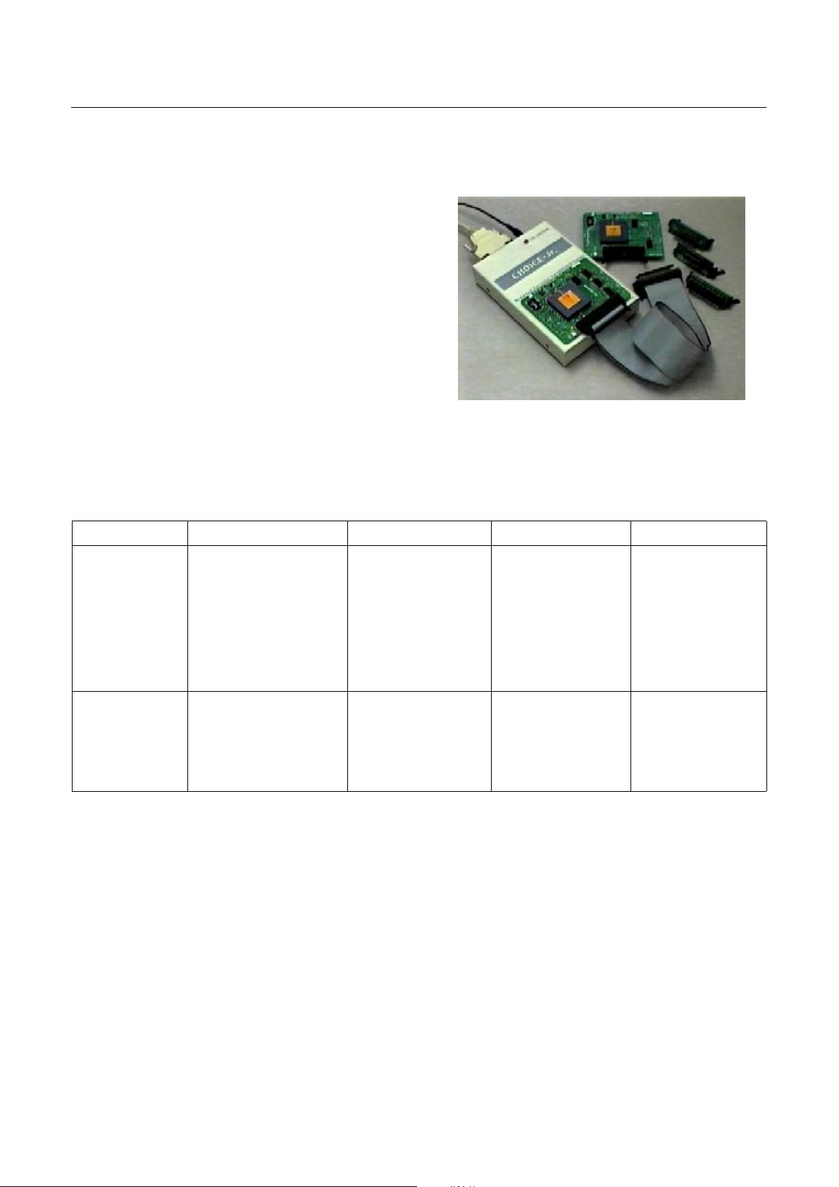
1.3 Development Tools
The GMS815xxB are supported by a full-featured macro
assembler, an in-circuit emulator CHOICE-Jr.
TM
and OTP
programmers. There are third different type programmers
such as emulator add-on board type, single type, gang
type. For mode detail, Refer to “22. OTP PROGRAMMING” on page 73. Macro assembler operates under the
MS-Windows 95/98
TM
.
Please contact sales part of Hyundai MicroElectronics.
1.4 Ordering Information
Device name ROM Size RAM size Package
Mask version
OTP version
GMS81508B K
GMS81508B Q
GMS81508B LQ
GMS81516B K
GMS81516B Q
GMS81516B LQ
GMS81524B K
GMS81524B Q
GMS81524B LQ
GMS81516BT K
GMS81516BT Q
GMS81516BT LQ
GMS81524BT K
GMS81524BT Q
GMS81524BT LQ
8K bytes
8K bytes
8K bytes
16K bytes
16K bytes
16K bytes
24K bytes
24K bytes
24K bytes
16K bytes OTP
16K bytes OTP
16K bytes OTP
24K bytes OTP
24K bytes OTP
24K bytes OTP
448 bytes
448 bytes
448 bytes
448 bytes
448 bytes
448 bytes
448 bytes
448 bytes
448 bytes
448 bytes
448 bytes
448 bytes
448 bytes
448 bytes
448 bytes
64SDIP
64MQFP
64LQFP
64SDIP
64MQFP
64LQFP
64SDIP
64MQFP
64LQFP
64SDIP
64MQFP
64LQFP
64SDIP
64MQFP
64LQFP
2 DEC. 1999 Ver 1.04
HYUNDAI MicroElectronics GMS81508B/16B/24B
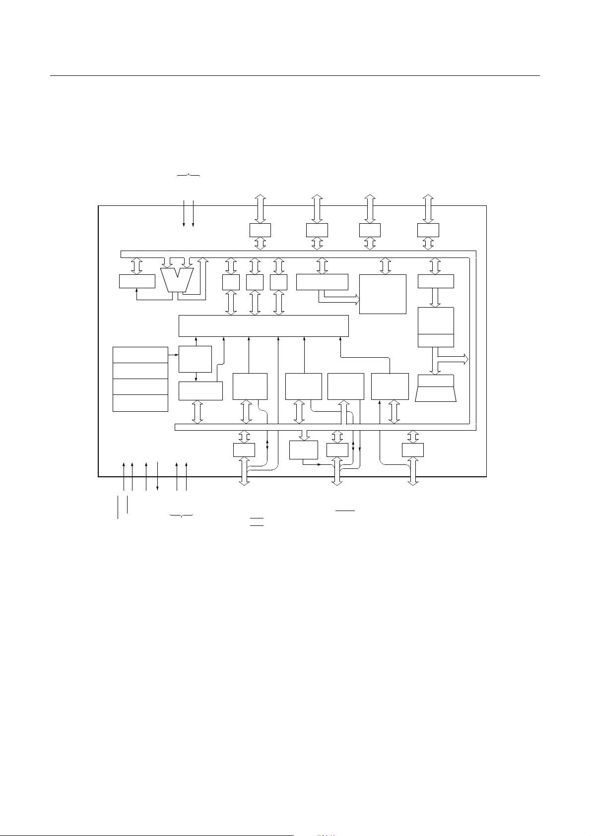
2. BLOCK DIAGRAM
ADC Power
Supply
PSW
System controller
System
Clock Controller
Timing generator
Clock
Generator
AVDDAV
ALU
8-bit Basic
Interval
Watchdog
Timer
Timer
SS
R00~R07
R0
A
X Y
Interrupt Controller
8-bit
Timer/
Counter
R4 R5
R10~R17
Stack Pointer
8-bit serial
Interface
Buzzer
Driver
R1
8-bit PWM
R20~R27
R2
Data Memor y
(448 bytes)
8-bit
ADC
R30~R37
R3
PC
Program
Memory
Data Table
PC
R6
TEST
RESET
IN
X
X
OUT
DD
V
Power
Supply
SS
V
R40 / INT0
R41 / INT1
R42 / INT2
R43 / INT3
R44 / EC0
R45 / EC2
R46 / T1O
R47 / T3O
R50 / SIN
R51 / SOUT
R52 / SCLK
R53 / SRDY
R54 / WDTO
R55 / BUZ
R56 / PWM0
R57 / PWM1
R60 / AN0
R61 / AN1
R62 / AN2
R63 / AN3
R64 / AN4
R65 / AN5
R66 / AN6
R67 / AN7
DEC. 1999 Ver 1.04 3

GMS81508B/16B/24B HYUNDAI MicroElectronics
3. PIN ASSIGNMENT
64SDIP
(Top View)
AN7
AN6
AN5
AN4
AN3
AN2
AN1
AN0
PWM1
PWM0
BUZ
WDTO
SRDY
SCLK
SOUT
SIN
T3O
T1O
EC2
EC0
INT3
INT2
INT1
INT0
V
DD
TEST
AV
SS
AV
DD
R67
R66
R65
R64
R63
R62
R61
R60
R57
R56
R55
R54
R53
R52
R51
R50
R47
R46
R45
R44
R43
R42
R41
R40
RESET
XIN
XOUT
V
SS
1
2
3
4
5
6
7
8
9
10
11
12
13
14
15
16
17
18
19
20
21
22
23
24
25
26
27
28
29
30
31
32
64
63
62
61
60
59
58
57
56
55
54
GMS81508B/16B/24B
53
52
51
50
49
48
47
46
45
44
43
42
41
40
39
38
37
36
35
34
33
R30
R31
R32
R33
R34
R35
R36
R37
R00
R01
R02
R03
R04
R05
R06
R07
R10
R11
R12
R13
R14
R15
R16
R17
R20
R21
R22
R23
R24
R25
R26
R27
64MQFP
(Top View)
AN7
AN6
R36
R35
R34
R33
R32
R31
R30
V
DD
TEST
AV
SS
AV
DD
R67
R66
R37
R01
R02
R03
R00
515049
52
53
54
55
56
57
58
59
60
61
62
63
64
484746
123456789
R65
R63
R62
R61
R64
AN5
AN3
AN2
AN1
AN4
R04
R05
R06
R07
R10
R11
R12
R13
45
4443424140
GMS81508B/16B/24B
R60
R57
R56
R55
AN0
PWM1
PWM0
BUZ
39
101112131415161718
R54
R53
R52
R51
SCLK
SOUT
SRDY
WDTO
R14
R15
R16
R17
3837363534
R50
R47
R46
R45
SIN
T3O
T1O
EC2
R20
R44
EC0
R21
33
R22
32
R23
31
R24
30
R25
29
R26
28
R27
27
V
26
SS
XOUT
25
XIN
24
23
RESET
R40
22
21
20
19
R43
INT3
R41
R42
INT0
INT1
INT2
4 DEC. 1999 Ver 1.04

HYUNDAI MicroElectronics GMS81508B/16B/24B
64LQFP
(Top View)
R00
R01
R02
R03
R04
R05
R06
R07
R10
R11
R12
R13
R14
R15
R16
R17
AN7
AN6
AN5
AN4
R37
R36
R35
R34
R33
R32
R31
R30
V
DD
TEST
AV
SS
AV
DD
R67
R66
R65
R64
484746454443424140393837363534
49
50
51
52
53
54
55
56
57
58
59
60
61
62
63
64
GMS81508B/16B/24B
123456789
R63
R62
R61
R60
R57
R56
R55
R54
AN3
AN2
AN1
AN0
PWM1
PWM0
BUZ
WDTO
10111213141516
R53
R52
SRDY
SCLK
R51
SOUT
33
32
R20
31
R21
30
R22
29
R23
28
R24
27
R25
26
R26
25
R27
24
V
SS
23
XOUT
XIN
22
21
RESET
20
R40
19
R41
18
R42
17
R43
R50
R47
R46
R45
R44
SIN
T3O
T1O
EC2
EC0
INT0
INT1
INT2
INT3
DEC. 1999 Ver 1.04 5
GMS81508B/16B/24B HYUNDAI MicroElectronics
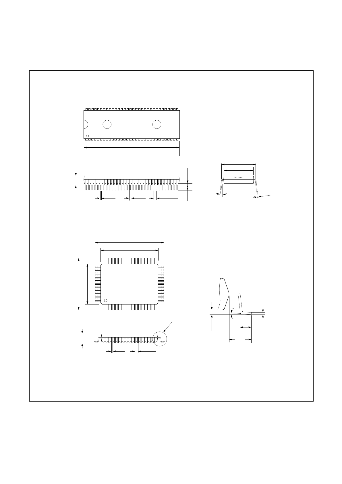
4. PACKAGE DIAGRAM
64SDIP
UNIT: INCH
2.280
2.260
0.750 Typ.
0.680
0-15
0.660
2
1
.0
0
8
0
.0
°
0
0.205 max.
min. 0.015
0.022
0.016
0.050
0.030
0.070 Typ.
0.140
0.120
64MQFP
18.15
17.65
3.18 max.
24.15
23.65
20.10
19.90
14.10
13.90
SEE DETAIL “A”
0.50
0.35
1.00 Typ.
0.36
0.10
UNIT: MM
0-7
°
1.95
REF
DETAIL “A”
1.03
0.73
0.23
0.13
6 DEC. 1999 Ver 1.04
HYUNDAI MicroElectronics GMS81508B/16B/24B
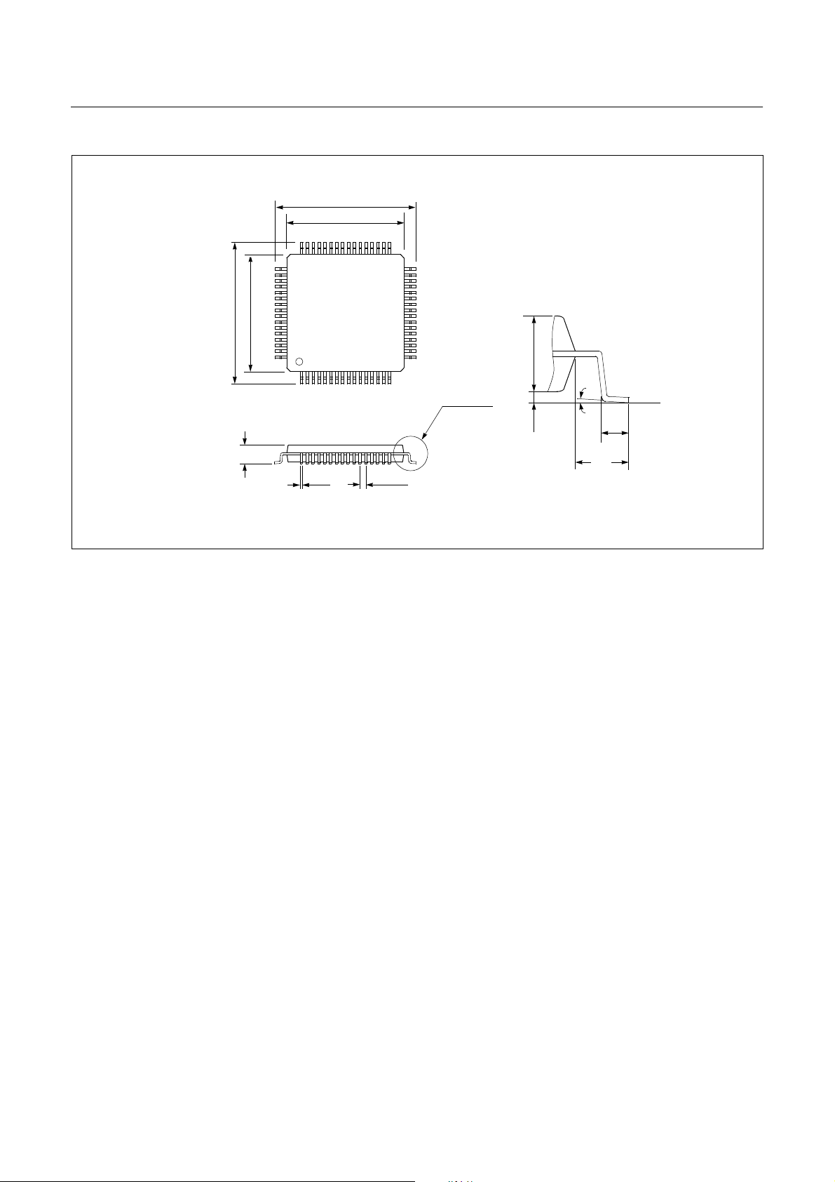
64LQFP
12.00 Typ.
10.00 Typ.
1.60 max.
12.00 Typ.
10.00 Typ.
0.38
0.22
0.50 Typ.
SEE DETAIL “A”
1.45
1.35
0.15
0.05
UNIT: MM
0-7
°
1.00
REF
DETAIL “A”
0.75
0.45
DEC. 1999 Ver 1.04 7

GMS81508B/16B/24B HYUNDAI MicroElectronics
5. PIN FUNCTION
V
: Supply voltage.
DD
V
: Circuit ground.
SS
TEST
: Used for Test Mode. For normal operation, it
should be connected to V
RESET
X
: Reset the MCU.
: Input to the inverting oscillator amplifier and input to
IN
DD
.
the internal main clock operating circuit.
X
: Output from the inverting oscillator amplifier.
OUT
R00~R07
: R0 is an 8-bit CMOS bidirectional I/O port. R0
pins 1 or 0 written to the Port Direction Register can be
used as output s or inputs.
R10~R17
: R1 is an 8-bit CMOS bidirectional I/O port. R1
pins 1 or 0 written to the Port Direction Register can be
used as output s or inputs.
R20~R27
: R2 is an 8-bit CMOS bidirectional I/O port. R2
pins 1 or 0 written to the Port Direction Register can be
used as output s or inputs.
R30~R37
: R3 is an 8-bit CMOS bidirectional I/O port. R3
pins 1 or 0 written to the Port Direction Register can be
used as output s or inputs.
R40~R47
: R4 is an 8-bit CMOS bidirectional I/O port. R4
pins 1 or 0 written to the Port Direction Register can be
used as output s or inputs.
In addition, R4 serves the functions of the various following special features.
used as outputs or inputs.
In addition, R5 serves the functions of the various follow -
ing special features.
Port pin Alternate function
R50
R51
R52
R53
R54
R55
R56
R57
R60~R67
SIN (Serial data input)
SOUT (Serial data output)
SCLK (Serial clock)
SRDY (Serial ready)
WDTO (Watchdog Timer output)
BUZ (Buzzer driver output)
PWM0 (PWM output 0)
PWM1 (PWM output 1)
: R6 is an 8-bit CMOS bidirectional I/O port. R6
pins 1 or 0 written to the Port Direction Register can be
used as outputs or inputs.
In addition, R6 is shared with the ADC input.
Port pin Alternate function
R60
R61
R62
R63
R64
R66
R66
R67
AN0 (Analog Input 0)
AN1 (Analog Input 1)
AN2 (Analog Input 2)
AN3 (Analog Input 3)
AN4 (Analog Input 4)
AN5 (Analog Input 5)
AN6 (Analog Input 6)
AN7 (Analog Input 7)
Port pin Alternate function
R40
R41
R42
R43
R44
R45
R46
R47
R50~R57
: R5 is an 8-bit CMOS bidirectional I/O port. R5
INT0 (External interrupt 0)
INT1 (External interrupt 1)
INT2 (External interrupt 2)
INT3 (External interrupt 3)
EC0
(Event counter input 0)
(Event counter input 2)
EC2
T1O (Timer/Counter 1 output)
T3O (Timer/Counter 3 output)
Note: On the MDS Ch oice, when the M CU is RESET, R60
can not be used digital input port. For more detail, refer to
"9. I/O PORTS" on page 31.
AV
: Supply voltage to the ladder resistor o f ADC cir-
DD
cuit. To enhance the resolution of analog to digital converter, use independent power source as well as possible, other
than digital power source.
AV
: ADC circuit ground.
SS
pins 1 or 0 written to the Port Direction Register can be
8 DEC. 1999 Ver 1.04

HYUNDAI MicroElectronics GMS81508B/16B/24B
PIN NAME In/Out
Function
Basic Alternate
V
DD
V
SS
TEST
- Supply voltage
- Circuit ground
I
Controls test mode of the chip,
For normal operation, it should be connected at VDD.
RESET I Reset signal input
X
X
IN
OUT
I Oscillation input
O Oscillation output
R00~R07 I/O 8-bit general I/O ports
R10~R17 I/O 8-bit general I/O ports
R20~R27 I/O 8-bit general I/O ports
R30~R37 I/O 8-bit general I/O ports
R40 (INT0) I/O (I)
External interrupt 0 input
R41 (INT1) I/O (I) External interrupt 1 input
R42 (INT2) I/O (I) External interrupt 2 input
R43 (INT3) I/O (I) External interrupt 3 input
R44 (EC0
R45 (EC2
) I/O (I) Timer/Counter 0 external input
) I/O (I) Timer/Counter 2 external input
8-bit general I/O ports
R46 (T1O) I/O (O) Timer/Counter 1 output
R47 (T3O) I/O (O) Timer/Counter 3 output
R50 (SIN) I/O (I)
Serial data input
R51 (SOUT) I/O (O) Serial data output
R52 (SCLK) I/O (I/O) Serial clock I/O
R53 (SRDY) I/O (I/O) Receive enable I/O
8-bit general I/O ports
R54 (WDTO) I/O (O) Watchdog timer overflow output
R55 (BUZ) I/O (O) Buzzer driving output
R56 (PWM0) I/O (O)
PWM pulse output
R57 (PWM1) I/O (O)
R60~R63 (AN0~AN3) I (I) General input ports
Analog voltage input
R64~R67 (AN4~AN7) I/O (I) General I/O ports
AV
AV
SS
DD
- Groun d level input pin for ADC
- Supply voltage input pin for ADC
Table 5-1 Port Function Description
DEC. 1999 Ver 1.04 9
GMS81508B/16B/24B HYUNDAI MicroElectronics
MUX
Data Bus
V
DD
V
SS
Pin
Data Reg.
Direction
Reg.
Rd
MUX
Selection
SCK Output
MUX
SCK Input
exck
MUX
Data Bus
V
DD
V
SS
Pin
Data Reg.
Direction
Reg.
Rd
MUX
Selection
SRDY Output
SRDY Input
SRDY
6. PORT STRUCTURES
R00~R07, R10~R17, R20~R27, R30~37
V
DD
Data Reg.
Dir.
Reg.
Data Bus
MUX
Rd
VSS
Pin
R40/INT0, R41/INT1, R42/INT2, R43/INT3, R44/
, R45/EC2, R50/SIN
EC0
Data Bus
Data Reg.
Direction
Reg.
PMR Selection
MUX
V
DD
Pin
V
SS
R52/SCLK
S53/SRDY
Rd
EX) INT0
Alternate Function
R46/T1O, R47/T3O, R51/SOUT, R54/WDTO
R55BUZ, R56/PWM0, R57/PWM1
Selection
Secondary function
MUX
Data Reg.
Data Bus
Direction
Reg.
MUX
Rd
V
DD
Pin
V
SS
10 DEC. 1999 Ver 1.04

HYUNDAI MicroElectronics GMS81508B/16B/24B
RESET
V
DD
V
SS
TEST
V
DD
V
SS
OTP version: disconnected
Mask version: connected
R60/AN0 ~ R63/AN3
Data bus
To A/D converter
R64/AN7 ~ R67/AN7
Data Reg.
Dir.
Reg.
Data Bus
MUX
Rd
Rd
RESET
V
DD
V
SS
TEST
V
DD
Pin
V
SS
X
, X
IN
XIN
XOUT
To A/D converter
OUT
V
DD
V
V
SS
SS
Stop
DEC. 1999 Ver 1.04 11
GMS81508B/16B/24B HYUNDAI MicroElectronics
7. ELECTRICAL CHARACTERISTICS
7.1 Absolute Maximum Ratings
Supply voltage.............................................-0.3 to +7.0 V
Storage Temperature ..................................-40 to +125 °C
Voltage on any pin with respect to Ground (V
................................ ..................................-0.3 to V
Maximum current out of V
Maximum current into V
Maximum current sunk by (I
Maximum output current sourced by (I
pin..........................150 mA
SS
pin ..............................80 mA
DD
per I/O Pin) ..........20 mA
OL
OH
)
SS
DD
per I/O Pin)
+0.3
...................................................................................8 mA
7.2 Recommended Operating Conditions
Parameter Symbol Condition
f
=1 ~ 10 MHz
XIN
f
Supply Voltage
Operating Frequency
V
f
DD
XIN
=1 ~ 8 MHz
XIN
f
=1 ~ 4 MHz
XIN
VDD=4.5~5.5V
VDD=2.7~5.5V
VDD=2.2~5.5V
Maximum current (ΣI
Maximum current (ΣI
)......................................100 mA
OL
)........................................50 mA
OH
Note: Stresses above those listed under “Absolute Maximum Ratings” may cause per manent damage to the d evice. This is a stress ra ting only and functional ope r ati on of
the device at any oth er c ond iti ons ab ov e tho se ind ic ated in
the oper ati o na l se c ti ons of this s pecificatio n i s no t i mp l ie d .
Exposure to absolute maximum rating conditions for extended periods may affect device reliability.
Specifications
Unit
Min. Max.
4.5
2.7
2.2
1
1
1
5.5
5.5
5.5
10
8
4
V
MHz
Operating Temperature
T
OPR
7.3 A/D Converter Characteristics
(TA=25°C, VSS=0V, VDD=5.12V@f
Parameter Symbol
Analog Input Voltage Range
Non-linearity Error
Differential Non-linearity Error
Zero Offset Error
Full Scale Error
Gain Error
Overall Accuracy
AV
Input Current I
DD
Conversion Time
=8MHz, VDD=3.072V@f
XIN
Normal Version
Temperature Extention Version
=4MHz)
XIN
Min.
V
N
N
N
N
N
N
T
CONV
AIN
NLE
DNLE
ZOE
FSE
GE
ACC
REF
V
SS
-
-
-
-
-
-
-0.51.01.0 mA
- - 40 20
-20
-40
85
85
Specifications
1
Typ.
f
XIN
-
1.0 ±1.5 ±1.5 LSB
±
1.0 ±1.5 ±1.5 LSB
±
0.5 ±1.5 ±1.5 LSB
±
0.35 ±0.5 ±0.5 LSB
±
1.0 ±1.5 ±1.5 LSB
±
1.0 ±1.5 ±1.5 LSB
±
Max.
=4MHz f
AV
DD
XIN
AV
=8MHz
DD
C
°
Unit
V
s
µ
12 DEC. 1999 Ver 1.04
HYUNDAI MicroElectronics GMS81508B/16B/24B
Specifications
Parameter Symbol
Min.
Analog Power Supply Input Range
1. Data in “Typ” column is at 25°C unless otherwise stated. These parameters are for design guidance only and are not tested.
AV
DD
0.9V
DD
Typ.
V
DD
1
f
XIN
Max.
=4MHz f
1.1V
XIN
DD
Unit
=8MHz
V
7.4 DC Electrical Characteristics
(TA=-20~85°C, VDD=2.7~5.5V, Ta= -20~85°C, f
=8MHz, VSS=0V)
XIN
Parameter Symbol Condition
, RESET,
X
IN
R4, R5, R6
R0, R1, R2, R3
, RESET,
X
IN
R4, R5, R6
R0, R1, R2, R3 -
R0,R1,R2,R3,R4,R5
R6
R0,R1,R2,R3,R4,R5
R6
@ T
=25°C0.9V
A
All input pins -5.0 - 5.0
All input pins -5.0 - 5.0
RESET, EC0, EC2,
SIN, SCLK, INT0~INT3
SS
Input High Voltage
Input Low Voltage
Output High Voltage
Output Low Voltage
Power Fail Detect
Voltage
Input High
Leakage Current
Input Low
Leakage Current
Hysteresis
V
IH1
V
IH2
V
IL1
V
IL2
V
OH
V
OL
V
PFD
I
IH1
I
IL
, V
V
T+
T-
I
DD1fXIN
VDD=4.5
VDD=2.7
VDD=4.5
V
=2.7
DD
VDD=4.5
VDD=2.7
I
=-2mA
OH1
VDD=4.5
VDD=2.7
I
=5mA
OL1
V
=3.0V
PFD
V
=2.4V
PFD
VIN=V
DD
VIN=V
SS
= 8 MHz A ll inp ut = V
C ry s ta l Oscilla tor ,
Power Current
1. Data in “Typ.” column is at 4.5V, 25°C unless otherwise stated. These parameters are for design guidance only and are not tested.
I
DD2fXIN
I
STOP
=4MHz
L1=CL2
=30pF
C
A ll inp ut = V
SS
,
Specifications
Min.
0.8V
0.7V
DD
DD
Typ.
-
-
1
-
-1.0
V
DD
-
PFD
--V
-1.0V
0.3 0.8 V
-820mA
410mA
-110µA
Max.
V
DD
V
DD
0.2V
0.3V
1.1V
+0.3
+0.3
DD
DD
PFD
Unit
V
V
V
A
µ
A
µ
DEC. 1999 Ver 1.04 13

GMS81508B/16B/24B HYUNDAI MicroElectronics
7.5 AC Characteristics
(TA=-20~+85°C, VDD=5V±10%, VSS=0V)
Parameter Symbol Pins
Operating Frequency
Oscillation Stabilizing
Time
External Clock Pulse
Width
External Clock Transi-
tion Time
Interrupt Pulse Width
RESET Input Width
Event Counter Input
Pulse Width
Event Counter Transi-
tion Time
f
XIN
t
ST
t
CPW
t
RCP,tFCP
t
IW
t
RST
t
ECW
t
REC,tFEC
Specifications
Min. Typ. Max.
X
XIN, X
X
X
IN
OUT
IN
IN
1.0 - 10.0 MHz
--20ms
40 - - ns
- - 20 ns
INT0, INT1, INT2, INT3 2 - -
RESET 8--
EC0, EC2 2--
EC0, EC2 - - 20 ns
Unit
t
SYS
t
SYS
t
SYS
XIN
INT0~INT3
RESET
EC1, EC2
t
0.8V
t
REC
SYS
DD
t
IW
= 1/f
t
ECW
XIN
t
FEC
t
RCP
t
t
RST
t
Figure 7-1 Timing Chart
CPW
t
ECW
t
CPW
-0.5V
V
DD
0.5V
t
FCP
IW
0.2V
DD
0.2V
DD
0.8V
DD
0.2V
DD
14 DEC. 1999 Ver 1.04
HYUNDAI MicroElectronics GMS81508B/16B/24B
7.6 Serial Interface Timing Characteristics
(TA=-20~+85°C, VDD=5V±10%, VSS=0V, f
Parameter Symbol Pins
Serial Input Clock Pulse
Serial Input Clock Pulse Width
Serial Input Clock Pulse Transition
Time
SIN Input Pulse Transition Time
SIN Input Setup Time (External SCLK)
SIN Input Setup Time (Internal SCLK)
SIN Input Hold Time
Serial Output Clock Cycle Time
Serial Output Clock Pulse Width
Serial Output Clock Pulse Transition
Time
Serial Output Delay Time
XIN
t
SCYC
t
SCKW
t
FSCK
t
RSCK
t
FSIN
t
RSIN
t
SUS
t
SUS
t
HS
t
SCYC
t
SCKW
t
FSCK
t
RSCK
s
OUT
=8MHz)
Specifications
Unit
Min. Typ. Max.
SCLK
SCLK
2t
SYS
+70
t
SYS
-8ns
-8ns
+200
SCLK - - 30 ns
SIN - - 30 n s
SIN 100 - - ns
SIN 200 - ns
SIN
SCLK
SCLK
t
SYS
t
SYS
4t
SYS
-30
-ns
-
16t
SYS
ns
ns
+70
SCLK 30 ns
SOUT 100 ns
SCLK
SIN
SOUT
t
0.8V
0.2V
FSCK
t
SCYC
t
RSCK
SUS
DD
DD
t
SCKW
t
t
FSIN
t
DS
0.8V
DD
0.2V
DD
Figure 7-2 Serial I/O Timing Chart
t
SCKW
t
HS
0.8V
DD
0.2V
DD
t
RSIN
DEC. 1999 Ver 1.04 15
GMS81508B/16B/24B HYUNDAI MicroElectronics
7.7 Typical Characteristic Curves
This graphs and tables provided in this section are for design guidance only and are not tested or guaranteed.
In some graphs or tables the data presented are outside specified operating range (e.g. outside specified
VDD range). This is for information only and devices
are guaranteed to operate properly only within the
specified range.
I
OH
(mA)
-12
-9
-6
-3
I
OH
VDD=4.5V
Ta=25°C
0
V
−
OH
0.3 0.6
R0~R6 pins
0.9 1.2
1.5
VDD-V
(V)
OH
I
OH
(mA)
-12
-9
-6
-3
I
0
V
−
OH
VDD=3.0V
Ta=25°C
0.3 0.6
OH
The data presented in this s ection is a statistical s ummary
of data collected on units from different lots over a period
of time. “Typical” represents the mean of the distribution
while “max” or “min” represents (mean + 3σ) and (mean
3σ) respectively where σ is standard deviation
R0~R6 pins
(V)
0.9 1.2
1.5
VDD-V
OH
−
V
I
OL
(mA)
20
15
10
IH1
(V)
0
I
5
0
V
4
3
2
1
V
−
OL
VDD=4.5V
Ta=25°C
0.2 0.4
V
−
DD
f
=8MHz
XIN
Ta=25°C
23
OL1
IH1
R0~R6 pins
0.6 0.8
XIN, RESET,
R4, R5, R6 pins
45
1.0
I
V
−
OL
VDD=3.0V
Ta=25°C
0.2 0.4
V
DD
f
=8MHz
XIN
Ta=25°C
1
OL2
V
−
IH2
23
I
OL
(mA)
20
15
10
5
V
OL
(V)
V
DD
(V)
6
0
V
IH2
(V)
4
3
2
1
0
R0~R6 pins
0.6 0.8
R0, R1, R2, R3 pins
45
1.0
6
V
V
(V)
(V)
OL
DD
16 DEC. 1999 Ver 1.04
HYUNDAI MicroElectronics GMS81508B/16B/24B
V
IL2
(V)
I
DD
(mA)
4
3
2
1
0
20
15
10
5
0
V
DD
f
XIN
Ta=25°C
I
−
DD
Ta=25°C
f
V
−
IL1
=8MHz
23
V
DD
= 8MHz
XIN
23
XIN, RESET
R4, R5, R6 pins
45
Normal Operation
4MHz
45
,
V
DD
(V)
6
V
DD
(V)
6
V
I
DD
(µA)
IL2
(V)
0.4
0.3
0.2
0.1
4
3
2
1
0
0
V
DD
f
XIN
Ta=25°C
1
I
STOP
V
−
IL2
=8MHz
23
V
−
DD
23
R0, R1, R2, R3 pins
45
Stop Mode
45
6
6
V
DD
(V)
85°C
25°C
-20°C
V
DD
(V)
Operating Area
f
XIN
(MHz)
Ta= -20~85°C
10
8
6
4
2
0
23
45
V
DD
(V)
6
DEC. 1999 Ver 1.04 17
GMS81508B/16B/24B HYUNDAI MicroElectronics
SP
01
H
Stack Address (100H ~ 1FEH)
Bit 15 Bit 087
Hardware fixed
00H~FE
H
8. MEMORY ORGANIZATION
The GMS81508B/16B/24B has separate address spaces
for Program memory and Data Memory. Pro gram memory
can only be read, not written to. It can be up to 24K bytes
8.1 Registers
This device has six registers that are the Program Counter
(PC), a Accumulator (A), two index registers (X, Y), the
Stack Pointer (SP), and the Program Status Word (PSW).
The Program Counter consists of 16-bit register.
A
X
Y
SP
PCH
Figure 8-1 Configuration of Registers
Accumulator:
PCL
PSW
The Accumulator is the 8-bit general purpose register, used for data operation such as transfer, temporary saving, and conditional judgement, etc.
The Accumulator can be used as a 16-bit register with Y
Register as shown below.
Y
A
Two 8-bit Registers can be used as a “YA” 16-bit Register
Figure 8-2 Configuration of YA 16-bit Register
X, Y Registers
: In the addressing mode which uses these
index registers, the register conten ts a re added to the specified address, which becomes the actual address. These
modes are extremely effective for referencing subroutine
tables and memory tables . The index regi sters also h ave increment, decrement, comparison and data transfer functions, and they can be used as simple accumulators.
Stack Pointer
: The Stack Pointer is an 8-bit register used
for occurrence interrupts and calling out subroutines. Stack
Pointer identifies the location in the stack to be accessed
(save or restore).
Generally, SP is au to mat ic ally upda t ed wh e n a s ubr outin e
ACCUMULATOR
X REGISTER
Y REGISTER
STACK POINTER
PROGRAM COUNTER
PROGRAM STATUS
WORD
Y A
of Program memory. Data memory can be read and written
to up to 448 bytes including the stack area.
call is executed or an interrupt is accepted. However, if it
is used in excess of the stack area permitted by the data
memory allocating configuration, the user-processed data
may be lost.
The stack can be located at any position within 100
1FF
of the internal data memory. The SP is not initialized
H
to
H
by hardware, requiring to write the initial v alue (the lo cation with which the use of the stack starts) by using the initialization routine. Normally, the initial value of “F E
” is
H
used.
Note: The Stack Pointer must be initialized by software because its value is undefined after RESET.
Example: To initialize the SP
LDX #0FEH
TXSP ; SP ← FEH
Address 01FFH can not be used as stack. Don not use
1FFH, or malfunction would be occurred.
Program Counter
: The Program Counter is a 16-bit wide
which consists of two 8-bit registers, PCH and PCL. This
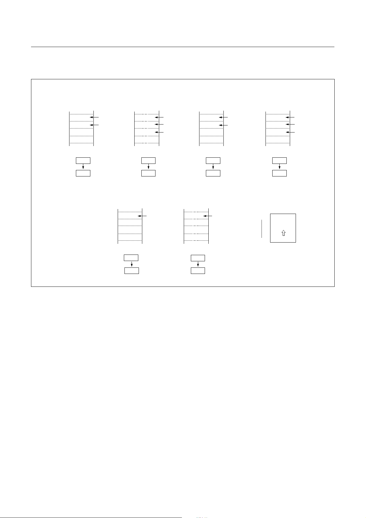
counter indicates the address of the next instruction to be
executed. In reset state, the program counter has reset routine address (PC
Program Status Word
:0FFH, PCL:0FEH).
H
: The Program Status Word (PSW)
contains several bits that reflect the current state of the
CPU. The PSW is described in Figure 8-3. It contains the
Negative flag, the Overflow flag, the Break flag the Half
Carry (for BCD operation), the Interrupt enable flag, the
Zero flag, and the Carry flag.
[Carry flag C]
This flag stores any carry or borrow from the ALU of CPU
after an arithmetic operation and is also changed by the
Shift Instruction or Rotate Instruction.
18 DEC. 1999 Ver 1.04
HYUNDAI MicroElectronics GMS81508B/16B/24B
[Zero flag Z]
This flag is set when the result of an arithmetic operat ion
MSB LSB
N
V G B H I Z C
NEGATIVE FLAG
OVERFLOW FLAG
when G=1, page is selected to “page 1”
SELECT DIRECT PAGE
BRK FLAG
PSW
Figure 8-3 PSW (Program Status Word) Register
[Interrupt disable flag I]
This flag enables/disables all interrupts except interrupt
caused by Reset or software BRK instruction. All interrupts are disabled when cleared to “0”. This flag immediately becomes “0” when an interrupt is served. It is set by
the EI instruction and cleared by the DI instruction.
or data transfer is “0” and is cleared by any other result.
RESET VALUE: 00
CARRY FLAG RECEIVES
CARRY OUT
ZERO FLAG
INTERRUPT ENABLE FLAG
HALF CARRY FLAG RECEIVES
CARRY OUT FROM BIT 1 OF
ADDITION OPERLANDS
H
This flag assigns RAM page for direct addressing mode. In
the direct addressing mode, addressing area is from zero
page 00
addressing area is assigned 100
to 0FFH when this flag is "0". If it is set to "1",
H
to 1FFH. It is set by
H
SETG instruction and cleared by CLRG.
[Overflow flag V]
[Half carry flag H]
After operation, this is set when there is a carry from bit 3
of ALU or there is no borrow from bit 4 of ALU. This bit
can not be set or cleared except CLRV instruction with
Overflow flag (V).
[Break flag B]
This flag is set by software BRK instruction to distinguish
BRK from TCALL instruction with the same vector address.
[Direct page flag G]
This flag is set to “1” when an overflow occurs as the result
of an arithmetic operation involving signs. An overflow
occurs when the result of an addition or subtraction exceeds +127(7F
) or -128(80H). The CLRV instruction
H
clears the overflow flag. There is no set instruction. When
the BIT instruction is executed, bit 6 of memory is copied
to this flag.
[Negative flag N]
This flag is set to match the sign bit (bit 7) status of the re-
sult of a data or arithmetic operation. When the BIT instruction is executed, bit 7 of memory is copied to this flag.
DEC. 1999 Ver 1.04 19
GMS81508B/16B/24B HYUNDAI MicroElectronics
At execution of
a CALL/TCALL/PCALL
01FE
01FD
01FC
01FB
SP before
execution
SP after
execution
PCH
PCL
01FE
01FC
Push
down
SP before
execution
SP after
execution
01FE
01FD
01FC
01FB
At execution
of PUSH instruction
PUSH A (X,Y,PSW)
01FE
01FD
01FC
01FB
A
01FE
01FD
At acceptance
of interrupt
PCH
PCL
PSW
01FE
01FB
Push
down
Push
down
01FE
01FD
01FC
01FB
At execution
of RET instruction
01FE
01FD
01FC
01FB
At execution
of POP instruction
POP A (X,Y,PSW)
PCH
PCL
01FC
01FE
A
01FD
01FE
Pop
up
Pop
up
At execution
of RET instruction
01FE
01FD
01FC
01FB
0100H
01FEH
PCH
PCL
PSW
01FB
01FE
Stack
depth
Pop
up
Figure 8-4 Stack Operation
20 DEC. 1999 Ver 1.04

HYUNDAI MicroElectronics GMS81508B/16B/24B
0FFE0H
E2
Address Vector Area Memory
E4
E6
E8
EA
EC
EE
F0
F2
F4
F6
F8
FA
FC
FE
-
-
Serial Communication Interface
Basic Interval Timer
-
-
-
External Interrupt 2
Timer/Counter 1 Interrupt
External Interrupt 0
-
RESET Vector Area
External Interrupt 1
Watchdog Timer Interrupt
“-” means reserved area.
NOTE:
Timer/Counter 2 Interrupt
External Interrupt 3
Timer/Counter 0 Interrupt
Timer/Counter 3 Interrupt
A/D Converter
8.2 Program Memory
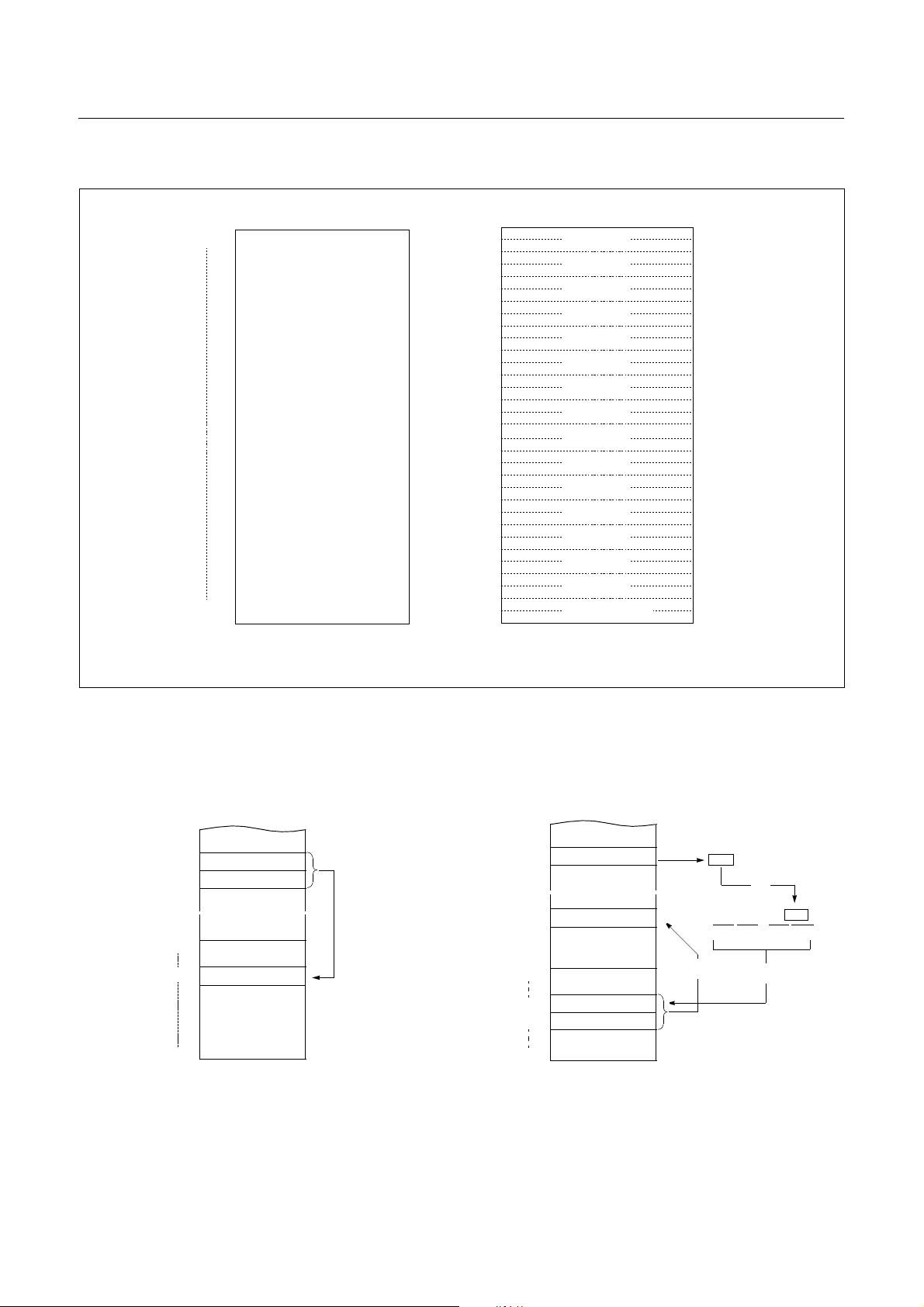
A 16-bit program counter is capable of addressing up to
64K bytes, but this device has 2 4K bytes program memory
space only physically implemented. Accessing a location
above FFFF
will cause a wrap-around to 0000H.
H
Figure 8-5, shows a map of Pr ogram Memory. After reset,
the CPU begins execution from reset vector which is stored
in address FFFE
and FFFFH as shown in Figure 8-6.
H
As shown in Figure 8-5, each area is assigned a fix ed location in Program Memory. Program Memory area contains
the user program.
A000
H
C000
H
E000
H
FEFF
H
FF00
FFC0
FFDF
FFE0
FFFF
H
H
H
H
H
TCALL area
Interrupt
Vector Area
PCALL area
GMS81508B, 8K ROM
GMS815024B, 24K ROM
GMS815016B, 16K ROM
it is more useful to save program byte length.
Table Call (TC ALL) causes the CP U to jump to each
TCALL address, where it commences the execution of the
service routine. The Table Call service area spaces 2-byte
for every TCALL: 0FFC0
for TCALL15, 0FFC2H for
H
TCALL14, etc., as shown in Figure 8-7.
Example: Usage of TCALL
The interrupt causes the CPU to jum p to specific location,
where it commences the execution of the service routine.
The External interrupt 0, for example, is assigned to location 0FFFA
interval: 0FFF8
0FFFA
Any area from 0FF00
. The interrupt service locations spaces 2-byte
H
and 0FFF9H for External Interru pt 1,
and 0FFFBH for External Interrupt 0, etc.
H
H
to 0FFFFH, if it is not going to be
H
used, its service location is available as general purpose
Program Memory.
Figure 8-5 Program Memory Map
Page Call (PCALL) area contains subroutine program to
reduce program byte length by using 2 bytes PCALL instead of 3 bytes CALL instruction. If it is frequently called,
DEC. 1999 Ver 1.04 21
Figure 8-6 Interrupt Vector Area
GMS81508B/16B/24B HYUNDAI MicroElectronics
11111111 11010110
01001010
PC:
FH FH DH 6H
4A
~
~
~
~
25
0FFD6
H
0FF00
H
0FFFF
H
D1
NEXT
0FFD7
H
➊
➋
➌
0D125
H
Reverse
Address
0FF00
0FFFF
PCALL Area Memory
H
PCALL Area
(256 Bytes)
H
Address P ro gra m Mem o r y
0FFC0
H
C1
C2
C3
C4
C5
C6
C7
C8
C9
CA
CB
CC
CD
CE
CF
D0
D1
D2
D3
D4
D5
D6
D7
D8
D9
DA
DB
DC
DD
DE
DF
NOTE:
* means that the BRK software interrupt is using
same address with TCALL0.
TCALL 15
TCALL 14
TCALL 13
TCALL 12
TCALL 11
TCALL 10
TCALL 9
TCALL 8
TCALL 7
TCALL 6
TCALL 5
TCALL 4
TCALL 3
TCALL 2
TCALL 1
TCALL 0 / BRK *
PCALL
→
→
→ →
rel
4F35 PCALL 35H
0FF00
0FF35
0FFFF
Figure 8-7 PCALL and TCALL Memory Area
TCALL
→
→
→ →
n
4A TCALL 4
4F
35
~
~
H
H
NEXT
H
~
~
22 DEC. 1999 Ver 1.04

HYUNDAI MicroElectronics GMS81508B/16B/24B
Example: The usage software example of Vector address for GMS81524B.
ORG 0FFE0H
DW NOT_USED
DW NOT_USED
DW SIO ; Serial Interface
DW BIT_TIMER ; Basic Interval Timer
DW WD_TIMER ; Watchdog Timer
DW ADC ; ADC
DW TIMER3 ; Timer-3
DW TIMER2 ; Timer-2
DW TIMER1 ; Timer-1
DW TIMER0 ; Timer-0
DW INT3 ; Int.3
DW INT2 ; Int.2
DW INT1 ; Int.1
DW INT0 ; Int.0
DW NOT_USED ; DW RESET ; Reset
; ORG 0C000H ; 16K ROM Start address
; ORG 0E000H ; 8K ROM Start address
;*******************************************
; MAIN PROGRAM *
;*******************************************
;
RESET: DI ;Disable All Interrupts
RAM_CLR: LDA #0 ;RAM Clear(!0000H->!00BFH)
;
;
ORG 0A000H ; 24K ROM Start address
CLRG
LDX #0
STA {X}+
CMPX #0C0H
BNE RAM_CLR
LDX #0FEH ;Stack Pointer Initialize
TXSP
LDM R0, #0 ;Normal Port 0
LDM R0DD,#82H ;Normal Port Direction
:
:
:
LDM TDR0,#250 ;8us x 250 = 2000us
LDM TM0,#1FH ;Start Timer0, 8us at 8MHz
LDM IRQH,#0
LDM IRQL,#0
LDM IENH,#0C8H ;Enable Timer0, INT0, INT1
LDM IENL,#0
LDM IEDS,#55H ;Select falling edge detect on INT pin
LDM PMR4,#3H ;Set external interrupt pin(INT0, INT1)
EI ;Enable master interrupt
:
:
:
:
NOT_USED:NOP
:
RETI
DEC. 1999 Ver 1.04 23

GMS81508B/16B/24B HYUNDAI MicroElectronics
8.3 Data Memory
Figure 8-8 shows the internal Data Memory space available. Data Memory is divided in to four groups, a user RAM,
control registers, Stack, and LCD memory.
0000
H
Note that unoccupied addresses may not be implemented
on the chip. Read accesses to these addresses will in general return random data, and write accesses will have an indeterminate effect.
More detailed informations of each register are explained
in each peripheral section.
User Memory
00BF
00C0
00FF
0100
01FF
H
H
H
H
H
Control
Registers
User Memory
or Stack Area
PAGE0
PAGE1
When “G-flag=0”,
this page is selected
When “G-flag=1”
Figure 8-8 Data Memory Map
User Memory
The GMS815xxB has 448 × 8 bits for th e user me mory
(RAM).
Control Registers
The control registers are used by the CPU and Peripheral
function blocks for controlling the desired operation of the
device. Therefore these registers contain control and status
bits for the interrupt system, the timer/ counters, analog to
digital converters and I/O ports. The control registers are in
address range of 0C0
to 0FFH.
H
Note: Write only registers can not be accessed by bit manipulation instruction. Do not use read-modify-write instruction. Use byte manipulation instruction, for example “LDM”.
Example; To write at CKCTLR
LDM CLCTLR,#09H
;Divide ratio(÷32)
Stack Area
The stack provides the area where the return address is
saved before a jump is performed during the processing
routine at the execution of a subroutine call instruction or
the acceptance of an interrupt.
When returning from the processing routine, execu ting the
subroutine return instruction [RET] restores the contents of
the program counter from the stack; ex ecuting the interrupt
return instruction [RETI] restores the contents of the program counter and flags.
The save/restore locations in the stack are determined by
the stack pointed (SP). The SP is automatically decreased
after the saving, and increased before the restoring. This
means the value of the SP indicates the stack location
number for the next save. Refer to Figure 8-4 on page 20.
24 DEC. 1999 Ver 1.04
HYUNDAI MicroElectronics GMS81508B/16B/24B
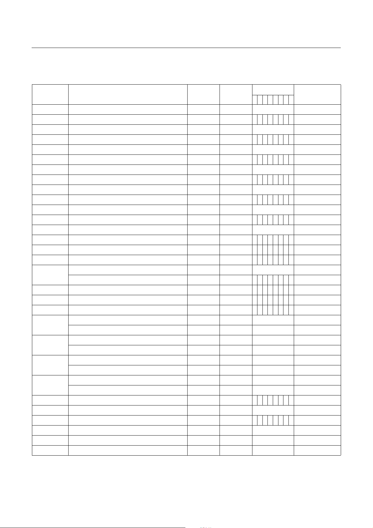
Address Register Name Symbol R/W
Initial Value
76543210
Page
00C0 R0 port data register R0 R/W Undefined page 31
00C1 R0 port I/O direction reg ister R0DD W 0 0 0 0 0 0 0 0 page 31
00C2 R1 port data register R1 R/W Undefined page 31
00C3 R1 port I/O direction reg ister R1DD W 0 0 0 0 0 0 0 0 page 31
00C4 R2 port data register R2 R/W Undefined page 31
00C5 R2 port I/O direction reg ister R2DD W 0 0 0 0 0 0 0 0 page 31
00C6 R3 port data register R3 R/W Undefined page 32
00C7 R3 port I/O direction reg ister R3DD W 0 0 0 0 0 0 0 0 page 32
00C8 R4 port data register R4 R/W Undefined page 32
00C9 R4 port I/O direction reg ister R4DD W 0 0 0 0 0 0 0 0 page 32
00CA R5 port data register R5 R/W Undefined page 33
00CB R5 port I/O direction register R5DD W 0 0 0 0 0 0 0 0 page 33
00CC R 6 port data register R6 R/W Undefined page 33
00CD R6 port I/O direction register R6DD W 0 0 0 0 - - - - page 33
00D0 R4 port mode register PMR4 W 0 0 0 0 0 0 0 0
00D1 R5 port mode register PMR5 W - - 0 0 - - - -
page 32, page 63
page 33, page 55
Basic interval timer mode register BITR R Undefined page 35
00D3
Clock contr ol register CKCTLR W - - 0 1 0 1 1 1 page 35
00E0 Watchdog Timer Register WDTR W - 0 1 1 1 1 1 1 page 64
00E2 Timer mode register 0 TM0 R/W 0 0 0 0 0 0 0 0 page 37
00E3 Timer mode register 2 TM2 R/W 0 0 0 0 0 0 0 0 page 37
Timer 0 data register TDR0 W Undefined page 37
00E4
00E5
Timer 0 counter register T0 R Undefined page 37
Timer 1 data register TDR1 W Undefined page 37
Timer 1 counter register T1 R Undefined page 37
Timer 2 data register TDR2 W Undefined page 37
00E6
Timer 2 counter register T2 R Undefined page 37
Timer 3 data register TDR3 W Undefined page 37
00E7
Timer 3 counter register T3 R Undefined page 37
00E8 A/D converter mode register ADCM R/W - - 0 0 0 0 0 1 page 47
00E9 A/D converter data register ADR R Undefined page 47
00EA Serial I/O mode register SIOM R/W - 0 0 0 0 0 0 1 page 49
00EB Serial I/O register SIOR R/W Undefined page 49
00EC Buzzer driver regi ste r BUR W Undefined page 55
00F0 PWM0 duty register PWMR0 W Undefined page 53
Table 8-1 Control Registers
DEC. 1999 Ver 1.04 25

GMS81508B/16B/24B HYUNDAI MicroElectronics
Address Register Name Symbol R/W
Initial Value
76543210
Page
00F1 PWM1 duty register PWMR1 W Undefined page 53
00F2 PWM control register PWMCR W 0 0 0 0 0 0 0 0 page 53
00F4 Interrupt enable register low IENL R/W 0 0 0 0 - - - - page 58
00F5 Interrupt request flag register low IRQL R/W 0 0 0 0 - - - - page 57
00F6 Interrupt enable register high IENH R/W 0 0 0 0 0 0 0 0 page 58
00F7 Interrupt request flag register high IRQH R/W 0 0 0 0 0 0 0 0 page57
00F8 External interrupt edge selection register IEDS W 0 0 0 0 0 0 0 0 page 63
00F9 Power fail detection register PFDR R/W - - - - 1 1 0 0 page 71
Table 8-1 Control Registers
W
R/W
- : this bit location is reserved.
Registers are controlled by byte manipulation instruction such as LDM etc., do not use bit manipulation
instruction such as SET1, CLR1 etc. If bit manipulation instruction is used on these registers,
content of other seven bits are may varied to unwanted value.
Registers are controlled by both bit and byte manipulation instruction.
26 DEC. 1999 Ver 1.04

HYUNDAI MicroElectronics GMS81508B/16B/24B
8.4 Addressing Mode
The GMS800 series MCU uses six addressing modes;
• Register addressing
• Immediate addressing
• Direct page addressing
• Absolute addressing
• Indexed addressing
• Register-indirect addressing
(1) Register Addressing
Register addressing accesses the A, X, Y, C and PSW.
(2) Immediate Addressing
→
→
→ →
#imm
In this mode, second byte (operand) is accessed as a data
immediate ly.
Example:
0435 ADC #35H
MEMORY
Example: G=1
E45535 LDM 35H,#55H
0135H
➊
0F100H
0F101H
0F102H
(3) Direct Page Addressing
data
~
~
~
~
data ¨ 55H
➋
E4
55
35
dp
→
→
→ →
In this mode, a address is specified within direct page.
Example; G=0
C535 LDA 35H ;A ←RAM[35H]
04
35
A+35H+C → A
When G-flag is 1, then RAM address is defined by 16-bit
address which is composed of 8-bit RAM paging register
(RPR) and 8-bit immediate data.
35H
0E550H
0E551H
data
➋
~
~
C5
35
~
~
data → A
➊
DEC. 1999 Ver 1.04 27
 Loading...