

Page 1
Page 2
HEWLETT-PACKARD
Technical Information from the Laboratories of Hewlett-Packard Company
JOURNAL
Contents-
processor-based
FEBRUARY 1981 Volume 32 • Number 2
A High-Purity, Fast-Switching Synthesized Signal Generator, by
phase noise and high frequency
Digital Control for a
Chisholm
Front-panel,
High-Performance
internal,
agility
are
Programmable Signal Generator, by Hamilton C.
and remote
usually
control
conflicting
of a complex instrument calls for a micro-
controller.
8662A Power-On and Self-Test Sequences, by Albert W.
Kovalick
Roland
requirements.
The ROM and RAM
Hassun
tests have some clever twists.
Low-Noise RF Signal Generator Design, by Dieter
liam J. Crilly, Jr., and Donald W.
Mathiesen
Scherer,
Bill S. Chan, Fred H.
Seven phase-locked loops and some innova-
tive techniques did the job.
A Switching Power Supply for a Low-Noise Signal Generator, by Gerald L Ainsworth
An
unusual
choice, because of switching noise, but the benefits outweighed the problems.
A High-Purity Signal Generator Output Section, by David L. Plan and Donald T.
This section
supplies
a low-noise output with unprecedented
level
accuracy.
Product Design for Precision and Purity, by Robert L DeVries Shielding and reliability
are major considerations.
Verifying High Spectral Purity and Level Accuracy in Production,
by
John W. Richardson
The question is how to test a state-of-the-art product without losing production-line efficiency.
Low
Ives,
Wil-
Borowski
In this Issue:
The quality of a precision laboratory signal generator is measured by how little noise and
spurious signals are present in its output along with the single-frequency signal that's
supposed to be there. No noise at all is an impossible ideal, but the subject of this issue, Model
| 8662A
I now available in its frequency range, which is 0.01 to 1280 megahertz.
I transmitters and receivers, and for testing this kind of equipment. In these systems, informaI tion is superimposed on a single-frequency carrier signal by modulating the carrier's
amplitude, frequency, or phase. A noisy carrier, one whose phase or amplitude jitters significantly, can severely
limit the performance of a system. Phase noise tends to be particularly troublesome, and so the measurement of
phase noise has become especially important. For phase-noise measurements, the 8662A is used as a stable
source with which to compare the equipment under test. These measurements are done in the development
laboratory, in production (where the 8662A's programmability makes automatic testing possible), and in
maintenance.
In receiver testing, an important measurement is adjacent channel selectivity, aimed at finding out how well a
receiver picks up a weak signal in one of its channels when there are strong interfering signals in adjacent
channels. A clean interfering signal is needed for this test so the performance that's measured is the receiver's
and not the signal generator's. Today, channels are being made narrower in an attempt to accommodate more
customers in an increasingly crowded electromagnetic spectrum. The narrower the channels, the cleaner the
test signal must be; hence the need for the 8662A.
Many applications lie above the 8662A's frequency range, but even in these cases, the 8662A's output can
often be multiplied to the needed frequency and still be clean enough, even though its phase noise is multiplied,
too. Our cover suggests an application like this. The 8662A feeds a step-recovery diode multiplier to provide the
transmitted signal in a pulsed Doppler radar system. (In practice, a pair of 8662As would be used to generate
both the transmitted signal and the receiver local oscillator signal). The radar scope in the foreground belongs to
the U.S. Federal Aviation Administration's Oakland TRACON (Traffic Control). This radar actually operates at
1030
MHz, within the 8662A's frequency range. We thank the FAA for letting us photograph it.
Synthesized
Signal Generator, comes as close to the ideal as any signal generator
Where are such super-clean, stable signals needed? Mostly in communications and radar
Illustrator, Nancy S. Vanderbloom • Administrative Services, Typography, Anne S. LoPresti • European Production Manager, Dick Leeksma
Editor, Richard P.
2 HEWLETT-PACKARD JOURNAL FEBRUARY 1981
Dolan
• Associate Editor, Kenneth A. Shaw • Art Director, Photographer, Arvid A. Danielson
©Hewlett-Packard
-R. P. Do/an
Company 1981 Printed in U.S.A.
Page 3
Fig. 1. Exceptionally low phase
noise and spurious output make
Model 8662A Synthesized Signal
Generator suitable for such demanding applications as receiver
adjacent channel
selectivity
measurements with closely spaced
channels and low-noise local oscil-
lator service. Fast frequency
switching and sweep capability
make the 8662A useful in
frequency-agile and swept local
oscillato applications. All functions are remotely programmable.
FEBRUARY 1981 HEWLETT-PACKARD
JOURNALS
Page 4
Spectral Purity
Spectral purity is a measure of how much the spectrum of the
output of a signal generator deviates from that of a pure sine wave.
Factors affecting spectral purity are:
• Phase noise, manifested as random fluctuations of zero crossings in the time domain and spectrum spreading in the fre-
quency domain
• AM noise, manifested as envelope fluctuations in the time domain and spectrum spreading in the frequency domain
•
Nonharmonically
called spurs
• Harmonically related sidebands caused by harmonic
distortion.
Phase noise is of particular importance in establishing the limits
of many modern communications systems. Harmonic distortion,
on the other hand, is not an important factor for the great majority
of applications in communications systems. It can be substan-
tially reduced by means of simple low-pass filtering.
AM noise levels are generally at least
levels in most signal sources. Furthermore, many operating systems rely on angle modulation (phase or frequency) and are
therefore not sensitive to AM noise.
Discrete sidebands can cause both amplitude and phase
modulation but occupy a much more restricted portion of the
spectrum than random modulation caused by random phase and
amplitude fluctuations.
The total unwanted power occupying a particular communication channel consists of the sum of the power in the discrete
sidebands plus the integral of the noise power in the channel
bandwidth. Both components therefore need to be minimized.
Phase Noise
The spectrum spreading of the carrier that is caused by the
existence of phase noise extends from less than 1 Hz offset from
the carrier to wherever the effect of additive
active device
MHz away from the carrier. Close-in phase noise is understood to
include offsets within 5 kHz of the carrier, while far-out phase
noise is understood to be that beyond 5 kHz.
Phase noise, or more generally, sideband noise (i.e., a combi-
nation of phase and AM noise), is responsible for limiting the
resolving power of heterodyne systems such as FM receivers and
spectrum analyzers. Resolving power in this case means the
ability to detect a small signal in the presence of a large one (see
Fig.
1).
Most mobile communications systems of the frequency multi-
plex kind have channel
6.25-kHz
high density of communications traffic. The system's ability to
extract a desired low-level signal from an undesired high-level
one (a nearby transmitter, for example) is limited by the sideband
noise of the receiver local oscillator and the selectivity of the IF
system. It is assumed in Fig. 1 that the received signals are
spectrally pure. In fact, any sideband noise on the undesired high-
level signal has the same effect as noise on the local oscillator.
low-noise sources to simulate the undesired high-level signal.
channel spacing is now used in some areas having a
Selectivity tests on high-quality mobile FM receivers require
related discrete sidebands, sometimes
10
dB below phase noise
noise—thermal
noise—begins
to dominate. This could be several
spacings
that exceed 5 kHz.
or
Forexample,
Close-in Phase Noise
Many modern developments have created a need for good
long-term stability and low close-in phase noise. Moving-targetindicator radars, navigation systems (e.g., Navstar), very-large-
baseline interferometry and PSK (phase-shift keying) represent
some of the applications where close-in phase noise plays a
major role.
The measurement of close-in phase noise on RF and microwave sources is becoming a very fundamental one, because
some crucial aspects of performance in the above-mentioned
systems are related to this effect.
A common application for a low-noise signal generator such as
the 8662A is as a reference source in phase-noise measurement
setups.1 The 8662A's combination of good long-term phase sta-
bility, excellent close-in phase noise and very good far-out phase
noise makes it possible to test signal sources at offsets from the
carrier ranging from fractions of a hertz to many MHz.
Frequency Agility
Several new communications networks have an additional requirement for frequency switching on the order of several milliseconds. To provide dynamic test conditions for these systems,
it is necessary for the test signal source to settle to a new frequency in somewhat under a millisecond.
The combination of this level of agility, low close-in and far-out
noise and spurious sidebands represents an unusual engineering
challenge. How these objectives were achieved in the 8662A is
discussed in the accompanying article.
Reference
1. D. Scherer, "Design Principles and Test Methods for Low Phase Noise RF and
Microwave Sources," Hewlett-Packard RF and Microwave Symposium,
-Roland
1979.
Hassun
This is accomplished by measuring the actual level with an
accuracy of ±0.5 dB at a large number of frequencies, de-
termining the proper error
4 HEWLETT-PACKARD JOURNAL FEBRUARY
correction,
'
storing this informa-
tion in ROM, and then using it to correct the errors in output
level as a function of frequency and attenuator setting. The
8662A's unprecedented level accuracy is essential for accu-
Page 5
rate receiver sensitivity measurements.
Although primarily designed for high signal purity, the
8662A's indirect-type oscillator switches frequency with a
typical 12 ms total switching time (to within 100 Hz). RF
settling time is 0.5 ms. For testing frequency-agile receiv-
ers, a special learn mode may be used with the HP-IB*
programming bus to drive frequencies directly from the
bus, with
500-ju.s
switching speed.
All other front-panel functions are programmable via the
HP-IB, which is a standard feature. The microprocessor also
provides powerful diagnostic and error routines to aid the
user and service routines to aid in maintenance.
Flexible Control
A major design objective of the front-panel layout was to
improve measurement efficiency so that engineering and
production test productivity could be increased. Key func-
tions are grouped centrally. Frequencies are key-set to 0.1
Hz (or 0.2 Hz) and levels to
0.1
dB resolution. Values can be
incremented or decremented with up/down keys or a rotary
knob after keying in the desired step size. A store/recall
function allows up to nine complete front-panel control
settings to be retained and recalled singly or in a sequence
of up to 10 steps.
Most increment and sequence steps can be triggered by
rear-panel inputs. A series of pins available on a rear-panel
connector allows certain commands to be executed when
one of the pins is connected to ground (a debounce circuit is
provided internally) or pulsed with a negative-going TTL-
compatible pulse of at least
5-/us
duration. This allows out-
puts to be tied back to inputs directly, thus creating a sequential system, or through decision-making logic. For
example, if the sweep output is tied to the step-up pin, the
whole frequency range of the 8662A can be sequentially
swept in specified increments. If a detector circuit and some
logic are also used, then the sweeping action can be stopped
whenever a signal is detected.
Powerful sweep capability that preserves synthesizer
stability, resolution, and accuracy makes the 8662A ideal
for characterizing high-stability components such as crys-
tal filters. Start/stop or span sweeps can be selected. Five
key-set markers plus linear or log sweep are available. By
using the sequence
function,
multiple sweeps can be ob-
served simultaneously.
Full signal-generator capability is provided, with high-
performance AM and FM modulation. AM rates to 40 kHz
are possible depending on modulation depth and carrier
frequency. FM deviations to 200 kHz and rates to 100 kHz
are available for external modulation inputs. A 400 or
1000-Hz
Architecture
internal source can be selected.
The architecture of the 8662A reflects the major design
goals, which included low phase noise close to the carrier
(less than 5 kHz offsets), low phase noise far from the car-
rier, submillisecond frequency switching speeds, spurious
sidebands more than 90 dB below the carrier,
0.1-Hz
fre-
quency resolution, and quality modulation capability.
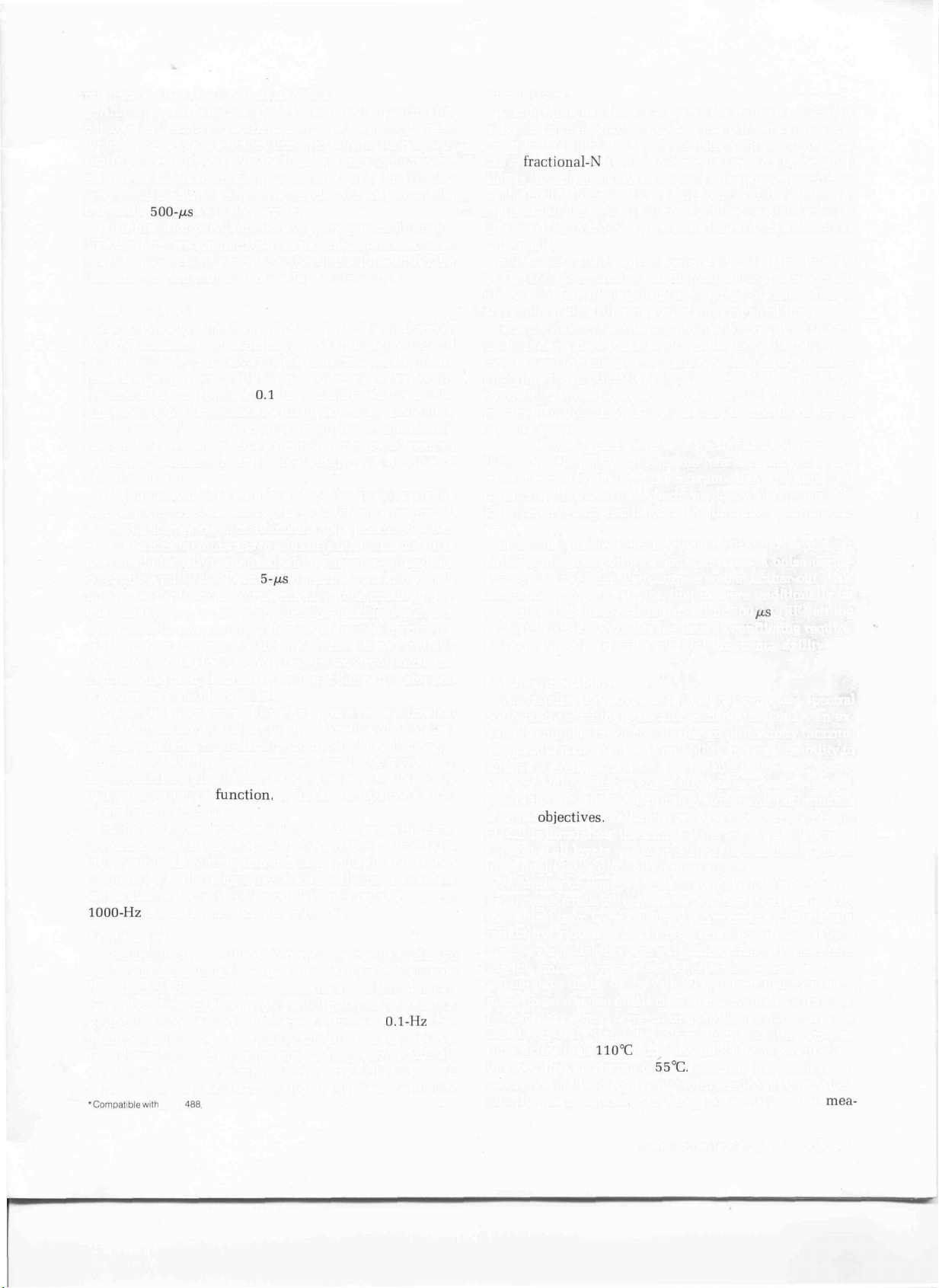
The phase-locked loop approach to frequency synthesis
was chosen because these objectives could be met with
a lower level of product complexity. Fig. 2 is the 8662A
•Compatible
with
IEEE
488
block diagram.
Divide ratios have been chosen so that noise on any of the
reference signals going into the phase detectors does not
undergo multiplication by more than 2 at the output. The
use of
fractional-N
divider techniques (see article, page 12)
allows the achievement of a specific frequency resolution
while maintaining a wider loop bandwidth (leading to
higher switching speed) than would be possible without
the use of fractional-N. At the same time, the divide ratio is
kept small.
Sidebands caused by reference signals leaking into the
VCOs (voltage-controlled oscillators) are kept below -100
dBc on the output signal in the majority of cases. This is
accomplished by filtering, isolation, and shielding.
The provision of frequency modulation required the ad-
dition of two phase-locked loops in the block diagram. One
loop is used to generate the frequency modulated signal by
applying the modulating signal to the VCO. The loop
bandwidth is less than the lowest modulating signal frequency. The other loop is used to sum the modulated signal
into the system.
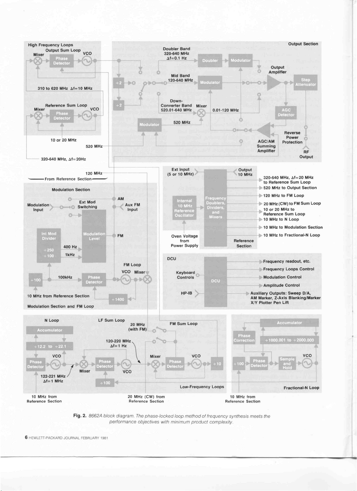
Fig. 3 shows typical 8662A single-sideband phase noise.
Below 10 kHz, phase noise of the reference section domi-
nates. From 10 to 500 kHz the reference loop and sum loop
determine the phase noise performance, while beyond 500
kHz the sum loop oscillator is the dominant phase noise
source.
This noise profile indicates that the HP 8662A is not only
an RF synthesizer with exceptional close-in noise perfor-
mance, but that it can also compete well at farther-out offset
frequencies where cavity oscillators were traditionally far
superior. With its switching speed of 500
/us
(RF settling
time), the HP 8662A meets the usually conflicting require-
ments of low phase noise and high frequency agility.
Assuring Reliability
The required improvements in signal generator spectral
purity and switching speed have made the 8662A an ex-
tremely complex product. The design philosophy for com-
plex products must include reliability and serviceability to
achieve operating cost levels acceptable to the user. There-
fore, reliability and serviceability goals were an integral
part of the early 8662A definition along with performance
and cost
objectives.
Reliability was the subject of significant
planning throughout the course of the project. Management
support at all levels was inspirational in steadfastly pursu-
ing a goal that is difficult to measure.
A number of steps were taken to make a substantial im-
provement in reliability. A series of educational sessions for
the project team were held by the corporate and divisional
reliability groups. The strong commitment of all team
members to reliability was a significant factor in maintain-
ing the emphasis over a period of several years.
The main thrust of the reliability effort in the develop-
ment phase was the creation of an environment within the
product that would favor component longevity. It was de-
cided very early to limit semiconductor junction tempera-
tures to less than
the specified maximum of
110°C
when the ambient temperature is at
55°C.
Junction temperature is a
parameter that is directly related to semiconductor failure
rate. It was measured by making body temperature
mea-
FEBRUARY 1981 HEWLETT-PACKARD JOURNAL 5
Page 6
Page 7
surements
using thermocouples on well over 100 components at several stages throughout the development cycle.
Junction temperature was then computed with the knowl-
edge of the power dissipated in the device and its published
junction-to-body thermal resistance. The goal was met with
the exception of a microwave transistor chip used in the
output amplifier, whose junction temperature can reach
125°C (computed) in the very worst case. The use of a
high-efficiency switching regulated power supply that
saves approximately 70W and a carefully planned thermal
design approach were necessities in achieving the junction
temperature goal.
Another step taken was the reduction of electrical stress
on the components used. Power dissipation, voltage and
current were checked on all transistors and passive compo-
nents. The reliability group helped establish safe derated
limits to which the designers adhered. Design margins on
such crucial parameters as phase-locked loop acquisition
ranges were made very substantial.
Humidity and condensation tests carried out in the
course of a battery of environmental tests revealed some
harmful chemical action. Growth of a clear, amorphous,
nonconducting substance gave rise to intermittent contact
between printed circuit board connector fingers and their
sockets. The microprocessor-based controller was espe-
cially vulnerable to this, since missing a single pulse can
change a legitimate instruction to an unintelligible stream
of information. A task force consisting mainly of product
assurance and printed circuit board processing groups
traced the problem to contaminants in the water used in
the wash cycle. They were eliminated and the problem
went away.
A number of assemblies containing novel designs were
put through life tests. This included prolonged periods of
operation at elevated ambient temperature
(55°C).
Two of
four switched reactance oscillators exhibited identical fail-
ure modes on the tenth and eleventh days of testing. A thin
layer of insulation was punched through causing a
mal-
function. The condition was corrected. The life tests proved
very useful in identifying a number of systematic problems
that generally only show up after lengthy periods of time
and may not be diagnosed as problems when not viewed in
the context of a disciplined test.
Furthermore, a sufficient number of prototypes were
built, operated almost continuously, and exercised
whenever possible to uncover weaknesses. This intensive
search for problems proved quite effective.
Most of the semiconductors used in the product are
burned in according to a program developed by HP's Stanford Park Division product assurance group. A 5:1 reduc-
tion in failure rate has been observed in a pilot program.
Failures detected are carefully analyzed and when systematic patterns emerge, the suppliers of the faulty devices
are notified.
Acknowledgments
The 8662A was a large project that spanned a considerable period of time. Many people have contributed to it in
various disciplines. The reliability of the product has benefitted both in planning and execution from the close involvement of the Stanford Park Division Reliability Group
under the leadership of Julius Trager, especially Randy
White and Charles Sallsey. Bill Whitney's leadership and
Gary Sprader's inputs were very valuable in the field of
serviceability. Introduction to manufacturing was planned
and organized by Bob
Ickes.
The long involvement of Marilyn Lawrence and Tom Cottrell as test technicians, together
with the assembly team of Shirley Flock and Edna Fleck,
was much appreciated by the R&D team. Marketing activity
was managed by Mike Gallagher. Original product defini-
tion benefited from the inputs of Ned Barnholt, Marc Saun-
ders and
Wally
Rasmussen. The development project took
place in the Stanford Park Division R&D lab managed by
John Page and was part of Brian Unter's R&D section re-
sponsibility. I also wish to acknowledge John Hasen's many
contributions as a member of the design team, especially in
the later stages of the project.
Roland Hassun
Roily
Hassun received his BSEE degree
from the Politecnico di
and his
MSEE
State University at San Jose in 1963.
He's also done graduate work at Stanford University.
he worked on the
studies on transistor noise, designed
synthesizers, and ultimately served as
project manager for the 8662A Signal
Generator. He's lectured on synthesizers and spectral purity on three
continents in three languages. This arti-
cle is his third contribution to the HP
Journal. A member
Computer Society, and
committee
nis, bridge and spy novels. He's interested in world affairs and has
served as an officer of a large philanthropic organization, receiving its
leadership award.
for
the IEEE's 1981 western convention. Roily enjoys ten-
AFCEA,
FEBRUARY
he's vice chairman of the program
1981
HEWLETT-PACKARD
Milano
degree from California
After
joining
41OC
of
the IEEE, the IEEE
in 1960
HP
in
1961,
Voltmeter, did
JOURNAL?
Page 8
Digital Control for a
High-Performance
Programmable Signal Generator
by Hamilton C. Chisholm
CURRENT PRODUCTION INSTRUMENT, the
Hewlett-Packard 8660A Synthesized Signal Gen-
A
erator, successfully demonstrates the concept of
keyboard control of a signal generator. By means of the
Hewlett-Packard Interface Bus
means of solving many instrumentation problems calling
for remote control. This previous development served as a
guide in the planning of the 8662A Synthesized Signal
Generator. Many enhancements were developed to pro-
vide full control of all parameters. The panel arrangement
provides the operator with easily understood parameter
control. Interaction with a responding parameter display
reinforces the learning of short key sequences. Where func-
tion control is not obvious from the front panel, a pullout
card beneath the instrument quickly provides assistance.
The
8662A
is basically a signal source of sinusoidal fre-
quencies with exceptional purity. With the addition of
amplitude control and selectable amplitude and frequency
modulation, the source becomes a signal generator. With
step time and step frequency control, the generator is en-
(HP-IB),*
it also provides a
hanced with frequency sweeping capabilities.
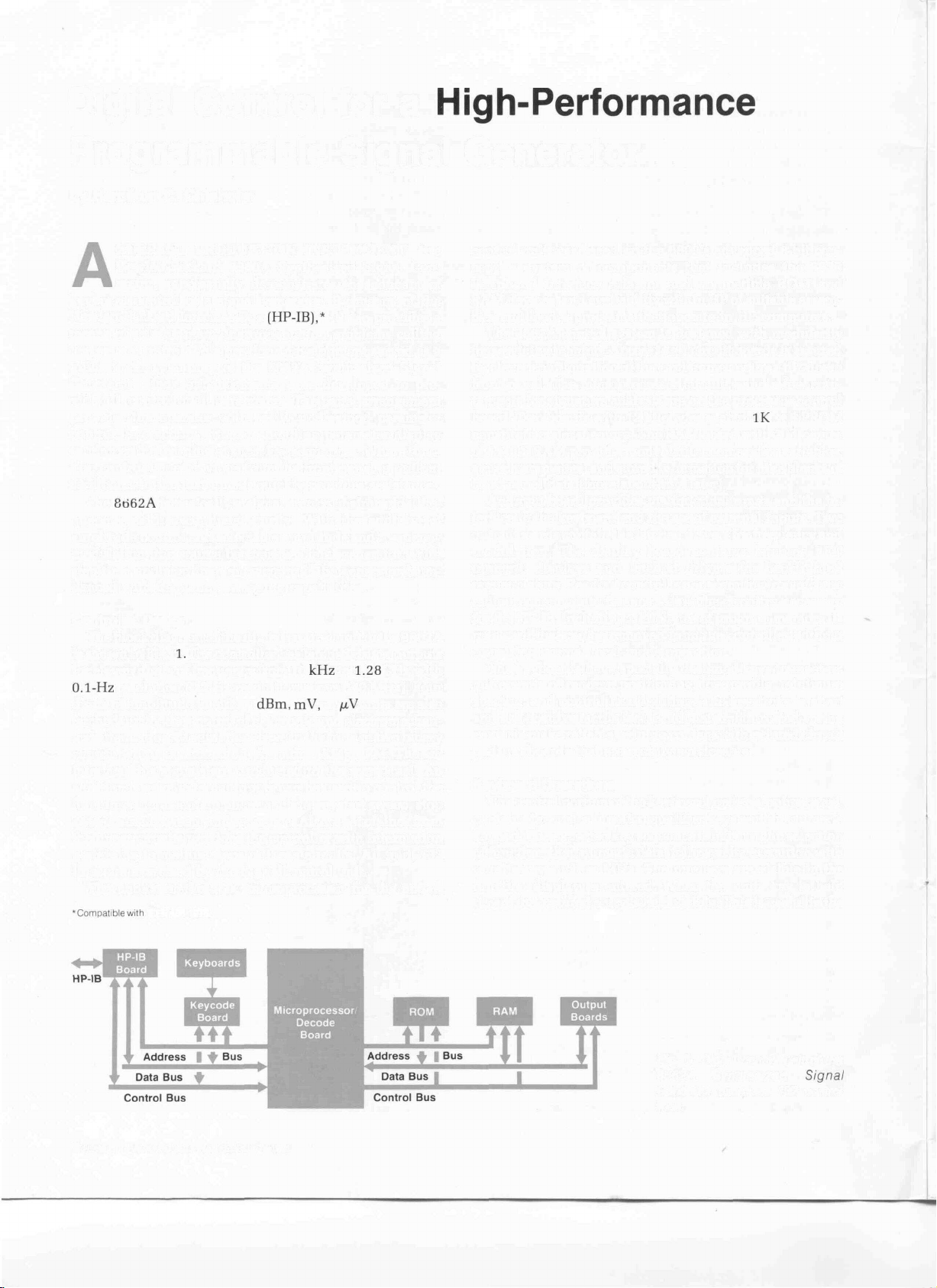
Controller Design
The block diagram of the digital control unit of the 8662A
is shown in Fig.
for eleven digits of frequency from 10
0.1-Hz
resolution (0.2-Hz resolution above 640 MHz). Four
digits of amplitude in either
latched out for the control of electronic and electromechan-
ical attenuation. Modulation drive in the form of two binary
control words is latched out for either AM or FM. The HP
Interface Bus signals are conducted to the rear panel. An
additional set of external inputs can be used to control the
functions increment up, increment down, start sweep, stop
sweep, single sweep, and sequence. Also, a set of lines from
1.
The controller has latched driver outputs
kHz
to
1.28
GHz with
dBm,
mV,
or
fj,V
units are also
the linear circuits provides the controller with information
pertaining to malfunctions of these circuits. All told, 132
lines are exercised by the digital control unit.
The choice of the 6800 microprocessor for the 8662A
•Compatible
with
IEEE 488-1978.
control unit was based on the 6800's advanced 8-bit concept, a system of components that includes the 6820
Peripheral Interface Adaptor and compatible ROM and
RAM devices, and availability within HP of suitable assem-
bler and loader programs that operate in HP computers.
The 8662A control system is designed with modularity
for servicing in mind. Access to all circuit boards is assured
by clever configuration of the card frame and by a tilt-down
front panel. The microprocessor circuitry and a few com-
ponents for signature analysis are on the processor control
board. Two boards with 12 kilobytes each of
constitute major memory. The RAM board with 2 kilobytes
of CMOS RAM provides nonvolatile memory for variables,
stored parameters, and stored information for nine blocks of
front-panel data (more about this later).
An input board provides malfunction inputs and the in-
terface to the keyboard and the set of external inputs. Two
output boards contain the latched drivers for frequency and
modulation. The display board contains latching LED
numeric displays and latched drivers for backlighted
nomenclature. Readout control is nonscanning to avoid any
radio frequency interference. All of the circuitry necessary
for the HP-IB, including 2 kilobytes of program memory, is
on a card that can be removed from the controller without
impairing normal local-mode operation.
The keyboards have specially designed keys to meet re-
quirements of random positioning, low profile, minimum
spacing, and control LED lighting. The keystroke is short
and has positive tactile feel. Gold plated, bifurcated spring
contacts make reliable, wiping contact with printed circuit
pads on boards that are readily serviceable.
Keyboard Operations
The central portion of the keyboard, on the sloping panel,
contains the major function qualifier keys and the numeric
keypad. The expected key sequence is left to right: selection
of function, then numeric data, followed by execution with
a units key such as MHz. The numbers are visible in the
function display as entered. When the units key is held
down, the justified entry is held visible. This is useful in the
IK
x 8 PROM
8 HEWLETT-PACKARD JOURNAL FEBRUARY 1981
Fig. 1. Digital control unit of the
8662A Synthesized
Generator exercises 132 control
lines.
Signal
Page 9
8662A Power-On and Self-Test
Sequences
by Albert W. Kovalick
With the introduction of microprocessor-based "smart" instruments, many conveniences were gained. However, some features of worth were lost. A typical instrument without a smart
controller has the ability to remember user settings by virtue of its
front-panel mechanical switches and dial settings. Most smart
instruments, on the other hand, require the user to key in most
front-panel settings each time power is switched on. An alternative is to use the HP-IB and program the instrument externally. For
simple stand-alone applications, however, manual initialization of
the instrument is a drawback.
The 8662A Synthesized Signal Generator solves this problem
by using a CMOS RAM powered by a battery to keep a record of
all front-panel settings. When the user turns off the synthesizer or
the power fails, the existing front-panel setting is saved. When
power is restored the last saved front-panel setting is restored.
Power-on Sequence
When the 8662A is switched on, a hardware power-on circuit
resets all hardware functions and causes the controller program
to begin. Before the settings are restored a checksum is com-
puted from the saved front-panel data. This is compared to a
reference checksum. If both checksums match, a software
routine restores all frequency, modulation, and amplitude settings. If the checksums disagree, RAM data has been altered.
This is unlikely, but it can occur if the battery discharges. In this
event, the first valid front-panel setting from the store/recall memory is recalled. If all nine settings contain altered data then a
default setting of 100 MHz and
RAM Testing
Testing of the entire 2K bytes of RAM is performed each time the
instrument is switched on. This power-on RAM test checks for
stuck bits in every RAM location without destroying any RAM data.
Before the test can begin, a small section or kernel of RAM is
tested. This kernel is needed to perform the larger 2K-byte test.
Each bit of RAM is now tested for the ability to
found faulty, a user code is displayed to indicate this. By use of a
special function code, a user may access this same test and run it
when desired.
A second, more extensive test is accessible by calling a routine
in the diagnostics ROM. It is different from the simpler test in three
ways. First, it checks for the case of multiple chips enabled.
Second, it tests for CMOS memory fade problems. Last, it tests for
row/column decoding errors internal to the chips. This test is
exhaustive. It runs for about
chips.
The test for multiple chips enabled must be performed before
decoding problems can be detected. If more than one RAM chip
is enabled, a read or write will affect more than the desired RAM.
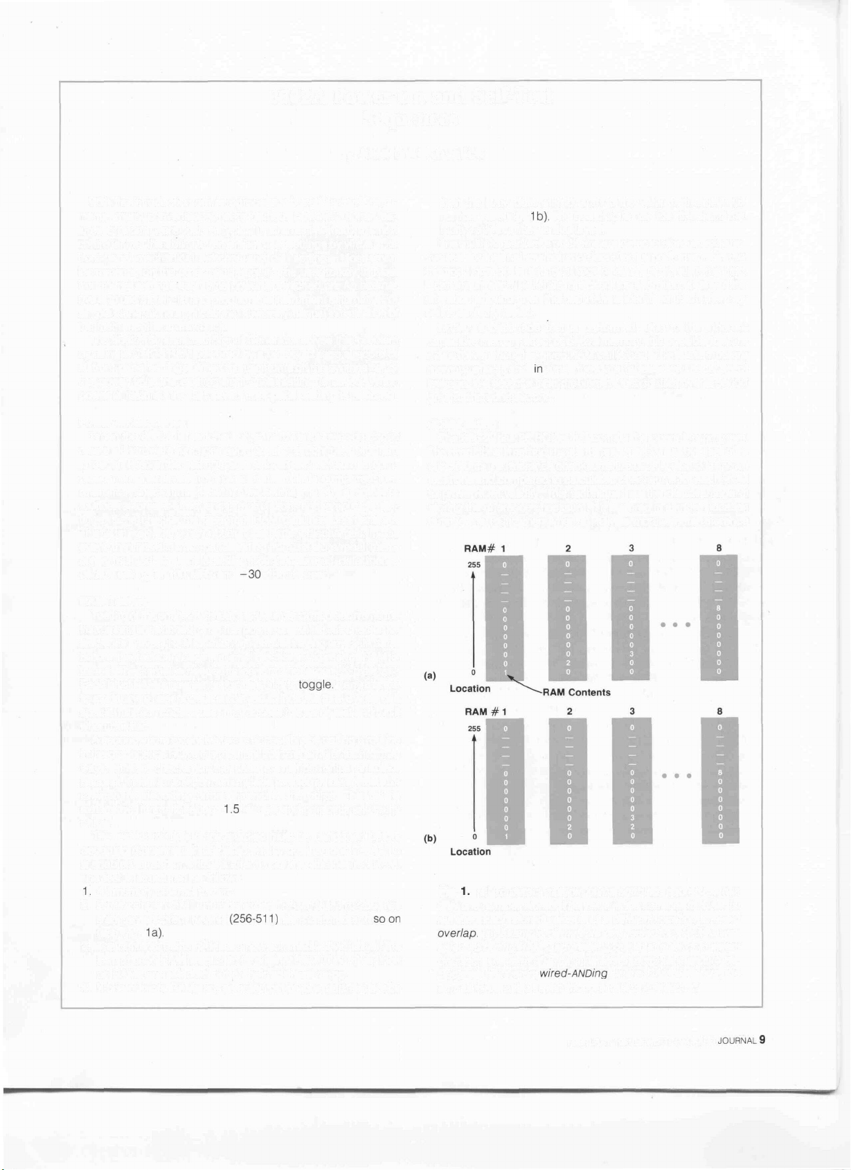
The test is structured as follows.
1.
All memory cleared to zero
2. Store a single RAM ID number in each RAM. RAM 1 (0-255) has
a solitary 1 stored. RAM 2
(see
Fig.
3. The contents of the RAMs are now summed individually. If the
sum of each RAM is equal to its original RAM ID number, then
no RAMs are selected out of their address range.
4. If one or more RAMs are selected out of their address space
1a).
-30
dBm is used.
toggle.
If any bits are
1.5
minutes and pinpoints any faulty
(256-511)
has a 2 stored and
soon
then the RAM data will not sum to the value of the RAM ID
number (see Fig.
faulty RAM number is displayed.
If no multiple read/write problems are detected then an exhaustive test for internal row/column decoding is performed. First, a
memory location is set to a known value. Next, all remaining
locations in each RAM are checked for alteration. If any data
alteration is found, then the bad RAM is identified. Each memory
1b).
The bad chip is now identified and the
cell is similarly tested.
Finally, a data fade test is performed. Due to the inherent
capacitive memory effect of CMOS memory, it is possible to store
a 1 or 0 even though a given RAM cell is bad. This is a temporary
memory effect, and
leakage. We detect a fade problem by testing data over a period
greater than one second.
ROM Testing
The 8662A has 26 ROMs that contain the operating program.
The traditional method used to test a ROM is by use of a
checksum. The reference checksums are usually stored in known
locations and compared to calculated checksums for each ROM
to prove ROM validity. This technique has the disadvantage of
storing the reference checksum. If it is stored in a known location
outside the ROM, then when a ROM is modified, its reference
Fig.
1.
(a) To detect multiple chips enabled, each RAM has
only one number stored. The value is the same as its RAM ID
number. Each stored value is at a different location to avoid
overlap,
(b) Example of multiple chip selection. RAM 3 was
selected during RAM 2 addressing due to a faulty chip select
decoder. The sum of RAM 3 data is 5, not 3 as it should be.
Because of inherent
sum of RAM 2 is 2, even though RAM 3 is selected.
in
time, the data fades away because of
wired-ANDing
on the RAM data bus, the
FEBRUARY 1981 HEWLETT-PACKARD
JOURNALS
Page 10
checksum must also be changed. Hence, two ROMs may need
changing. On the other hand, if each ROM has its checksum
stored within it, then an exact location is required and this may
interrupt the program code.
We have chosen to allocate the negative value of the checksum
dynamically. Suppose a sequence of assembly language code
could be produced that would not affect program operation and
would rarely, if ever, be produced by a programmer. A branch
around a
Once the program development is almost complete, this two-line
code segment
After assembly is complete the machine code is run through a
second program to locate the two-line segment. Next, this program computes the checksum of all ROM data excluding the NOP.
The NOP is then replaced by the two's complement of the
checksum. The controller program is not affected by this change
MOP
(no operation) falls into this category.
PROGRAM CODE
BRA +3
NOP
PROGRAM CODE
is
inserted roughly into the middle of each ROM.
due to the branch. Computing the checksum of a given ROM
yields zero as a result if all data is valid. The programmer never
needs to worry about the value of the checksum or the
location. To allow for easy ROM identification the actual value of
the total computed checksum can be one for ROM
ROM #2, and so on. This allows for easy detection of
ROMs.
Albert W. Kovalick
Al
Kovalick joined HP in
receiving his MSEE degree from the
University
He's designed printer drive circuitry
for handheld and desktop cal-
culators and contributed to the design of the controller software and
power supply of the 8662A Signal
Generator. He's named as an inven-
tor on two patents and three pend-
ing patents. Al was born
Francisco and now lives in Santa
Clara, California. His wife, who
works in HP's R&D labs as a programmer, has also contributed an
article to the HP Journal. Al is active in his church and enjoys read-
ing, woodworking, racquetball, and recreational mathematics.
of California at Berkeley.
MOP
#1,
two for
misloaded
1974
after
in
San
frequency mode where the display may be configured for
sweep display while a new parameter is entered. Should the
operator begin an entry but not complete
it,
the display can
be restored by striking any function select key.
The
INCR
SET key is
common
to all
function
keys
and a
function key qualifies its use in entering increment values.
The justified value may be viewed on entry by holding the
units key down. An increment value may be viewed at any
time
by
selecting
the
function,
then
holding
the
INCR
SET
key down.
The right-hand position of the keyboard contains mod-
ifiers in the form of increment up and down keys and a
rotary control for manual tuning. The increment up and
down keys are qualified by the selected function. Holding
either key down will cause a succession of increments at a
rate
of two per
second.
The
rotary
RESOLUTION
control
is
enabled for every new function by pressing either the x 10 or
-MO
key. Holding either of these down will enable blinking
of a digit that denotes the resolution digit to which the
rotary control will apply. The digit may be moved by re-
peatedly keying
x10
or
-MO
to get ten times more or less
resolution.
The
increment
value
previously
entered
via the
INCR
SET
key may be used by the rotary control as its entry value. This
mode is enabled by pressing the blue key and then the
key,
which
has the
shifted
function
INCR
printed
beside
-MO
it.
Another useful mode is the separation of rotary control
operation from the increment key operation with respect to
function. For example, while in the amplitude mode, the
blue
key and
shift
key
HOLD
(x 10) are
pressed
in
succession.
Then when frequency is selected as the operating function,
the amplitude may be adjusted with the rotary control and
the frequency incremented with the increment up and
down keys.
Sweep Control
The left-hand keyboard contains all the sweep parameter
keys. Either a start/stop sweep or a span-type sweep may be
selected. Parameters are entered, for instance, by keying
START
FREQ,
numerics
and
units.
The start/stop sweep may be reversed by giving start a
larger frequency value than stop. The sweep step size and
step time keys indicate the selected value with integral
LEDs. Once selected, the values are remembered. A change
from span to start/stop sweep, with different step size and
time values, will be indicated by the LEDs in the keytops.
Execution
of
AUTO
or
SINGLE
sweep
will
cause a split
dis-
play in the frequency window, five digits for each of the two
frequency
parameters.
When
MANUAL
sweep
is
selected,
full eleven-digit sweep frequency display is presented.
Control of the sweep is provided by dedicated use of the
rotary knob in the right-hand portion of the keyboard. Any
signal generator parameter value may be changed while in
the sweeping mode.
Up to five digital sweep frequency markers are selectable.
Each marker is entered as a frequency. The rear-panel out-
put for sweep markers provides Z-axis beam intensifying
potential to give a bright CRT spot on an oscilloscope. Each
spot may be identified on the CRT by holding the selected
marker key down. Each marker may be moved on the CRT
by means of the increment keys or the rotary control. When
a marker key is held down, its frequency value is displayed.
Front-Panel Storage
To ease user operation of the 8662A, nine front-panel
configurations can be stored in memory. Each stored con-
figuration includes every parameter set on the front panel.
Thus at any time, any of several totally different panel
configurations can be recalled. This helps to reduce test
setup time.
a
10 HEWLETT-PACKARD JOURNAL FEBRUARY 1981
Page 11

Coupled with the store/recall feature is a sequence opera-
tion. A sequence is the order in which the user desires to
recall previously stored settings. For example, assume there
is a linear sweep in store 1, a logarithmic sweep in store 3
and a frequency modulated carrier in store 7. These may be
useful for a given series of tests. The sequence 137 can now
be stored in the sequence memory, and each time the SEQ
key is pressed the next front panel, as ordered by the sequence memory, will be recalled.
Status Indication
The 8662A features a STATUS key, which is
LED-lighted
to signal the operator. Whenever it lights up and the key is
pressed and held, a double-digit code appears in the frequency window. The code can be interpreted by referring to
the pullout card beneath the instrument. Status messages
may concern the condition of the crystal oven temperature,
or indicate that an external oscillator standard is being
used. Operator guidance messages are typically concerned
with parameters out of range for the operating conditions.
The status indicator flashes for malfunctions detected
internally. Examples are a loop unlock condition or a fault
detected by a circuit monitoring a set of interface lines. The
latter provide extensive information about approximately
80 lines passing between controller and mainframe circuits.
These give early indications of circuit or cabling failures.
Servicing
The operator may call for a check on ROM or RAM with a
special function key sequence. The ROM test (see page 9) is
based on checksum routines and responds in case of a ROM
1C
failure with a double-digit code in the
display,
defining
the failed part. The RAM test will do the same for some
bit-type failures. More subtle failures require more detailed
testing, which is available in servicing routines. The latter
are part of a switch selectable set, which also includes rou-
tines for signature analysis testing with the HP 5004A Signal
Analyzer. Basically, control unit servicing is performed
using signature analysis. For extreme conditions where the
instrument does not respond to power-on, a fundamental
free-run test permits checks of the microprocessor board,
which is the key to further operation. This can be done
without any other boards in the system, thus aiding discov-
ery of stuck address and data buses and control lines. With a
correctly operating processor board, the special diagnostics
ROM and a program select switch on the board are used to
select a routine to stimulate the other system boards. Signatures at significant circuit points quickly give direction to
the service person and lead to discovery of the offending
component on the failed system board.
Production Testing
Production testing of the 8662A control unit uses signature analysis techniques almost exclusively. These
techniques are aided by using an HP 9825 Computer as
memory for all the circuit mode signatures and as a testing
guide. The technician instructs the computer with inputs
defining the system board and the integrated circuit under
test. As the device pins are probed, the computer reads the
input signature via the HP 5004A with a special modification. A comparison is made with the known good signature
in memory. An audible beep announces that the signature is
good and the technician can proceed to the next node without looking away from the circuit. When an errant signature
is encountered, the computer prints out the node location
on its paper tape.
A further testing development uses the computer with a
special multiplexer that can select any one of over 200 lines.
Suitable cabling connects all the control output interface
lines into the multiplexer. Computer programs are accessed
for a series of tests that automatically monitor all the cabled
lines and record information on any failures. This test has
special merit, since it tests driving
circuits,
connectors, and
cables in the signal path, any of which can experience
difficulties in the assembly operations.
Acknowledgments
Many people contributed to the concept and design of the
control unit, which includes the front-panel display and
keyboard arrangement. The key members of the design staff
and their contributions were: Walt Jimison for
major
portions of the hardware design and associated software, Han
Park for major software contributions to the control of the
display, frequency sweeping, and sweep markers, Dan
Derby and Jim Stewart, industrial designers, for their important contributions to the subtleties of panel design, Bill
Thomas, production engineer, for a major effort in applying
signature analysis with calculator control to production
testing, and Lloyd
Marrugg,
production engineer, for devoted effort in the transfer of the controller from engineering to production, effectively coping with the training of
personnel. To Bill West goes a special thanks for a superlative effort in designing the
keyswitches
now used exten-
sively in Hewlett-Packard instruments.
Hamilton C. Chisholm
Ham Chisholm received his BEE degree in
1948
from the University of Minnesota. He designed some of the first
solid-state counters in
of the first integrated circuit counters in
1968.
He's
and is named inventor on several patents. With HP since
the 5590A Nuclear Sealer and served
as project leader
sections of the 8660A, 8660C, and
8662A Signal Generators. He has
served in the U.S. Air Force as a flight
navigator and is a member of the IEEE.
Ham enjoys gardening, photography,
camping, and skiing. A native of Minneapolis, Minnesota, he now
lives in Los Altos, California. He and his wife have a son and a
grandson.
published several papers
1954
and some
1966,
he worked on
for
the digital control
FEBRUARY 1981 HEWLETT-PACKARD JOURNAL 11
Page 12

Low-Noise RF Signal Generator Design
by
Dieter
Scherer,
Bill
S. Chan, Fred H.
Ives,
William J. Crilly, Jr., and Donald W. Mathiesen
N THE RF DESIGN of the 8662A Synthesized Signal
Generator, novel techniques had to be developed to
combine low phase noise and low spurious signals with
I
the usually conflicting goal of high frequency agility. The
design was governed by the following objectives:
• Excellent spectral purity. Phase noise and spurious
,
nals
were to be low enough to allow, for example, re-
ceiver
out-of-channel
with very pure cavity-tuned signal generators.
• High frequency agility. RF settling was to occur in less
than 500
• Economic frequency resolution.
be achieved with a minimum number of loops and
minimum parts count.
Fig. 2 on page 6 shows the basic blocks of the resulting RF
design. These include the following functional blocks:
• The reference section
• The reference sum loop
• The output sum loop
• The low-frequency loops
• The
• The doubler, dividers and down-converter of the output
section.
All frequencies are directly or indirectly generated from a
10-MHz crystal oscillator or an external 5 or 10-MHz refer-
ence source. The reference section transforms the 10-MHz
reference signal into an RF reference signal that can step
from 320 to 640 MHz in 20-MHz steps.
In the reference loop this spectrum is filtered and ex-
panded into a 310-to-620-MHz range with 10-MHz steps.
The output sum loop combines this with a 10-to-20-MHz
signal with
loops, yielding the 320-to-640-MHz baseband with 0.1-Hz
resolution. This band is then heterodyned, divided down
and doubled to produce the 10-kHz-to-1280-MHz output of
the synthesizer (see article, page 22).
/xs.
fractional-N
0.1-Hz
testing previously only possible
0.1-Hz
resolution was to
loop
steps generated in the low-frequency
sig-
Direct Synthesis Reference Section
The reference section provides the following group of
frequencies:
1. 320 to 640 MHz every 20 MHz.
2. A switched 520 MHz to the output section down-
converter.
3. Switched 20 and 120 MHz to the FM sum loop.
Fig.
1.
The reference section directly synthesizes low-noise
reference signals for the 8662A's phase-locked loops. The
320-to-640 MHz band is generated with a mixer and eight
frequencies, as shown.
12 HEWLETT-PACKARD JOURNAL FEBRUARY 1981
Fig. 2. 8662A reference section derives various frequencies
by multiplying, dividing, and mixing the output of the internal
crystal
reference oscillator or an external standard.
Page 13

4. A selectable 10 or 20 MHz to the reference sum loop.
5. 10 MHz distributed to five other sections.
It was considered important that these frequencies be obtained with as low a noise contribution as achievable and
with undesired signals down 40 dB at the 320-to-640-MHz
reference output.
As Fig. 1 shows, the 320-to-640-MHz band may be generated with a mixer and eight frequencies. Using dc allows
the 320, 480, or 640-MHz signal to pass through the mixer.
Otherwise, two RF frequencies are generated
fir),
and the undesired frequency is eliminated by the refer-
(f^y = fLo
—
ence sum loop. Fig. 2 explains the generation of reference
signals in more detail.
Noise and Undesired Signals
Particular care was exercised in the design of the
amplifier and multiplier stages immediately following the
crystal oscillator to keep from degrading its noise performance. The amplifiers and doublers at higher frequencies
are not so critical since the phase noise of the 10-MHz
standard is increased by 6 dB each time the frequency is
doubled.
The multiplier selected is essentially a full-wave rectifier
circuit using Schottky diodes. This arrangement was
selected for the repeatability of low-noise performance, inherent rejection of the driving frequency (alleviating some
filtering problems), and convenience in generating a frequency at every octave of 10 MHz.
The amplifiers operate with low currents and high
voltages to keep the
1/f
noise current of the device low.
RF emitter degeneration decreases device nonlinearity,
which partly prevents 1/f noise from being converted to the
signal frequency.
The reference block has two stages of crystal filtering at
40 and 160 MHz. The filters serve the dual purpose of
removing 10 and 20-MHz sidebands not
rejected
by the
doublers and filtering the multiplied noise of the frequency
standard beyond approximately ±0.008% of center frequency. Multiplying 10 MHz to 640 MHz would result in a
36-dB phase-noise increase. The crystal filters must suppress the 10 and 20-MHz sidebands such that these
sidebands on the 520-MHz output are 90 dB below the
carrier, since they would be translated directly to the output
in the heterodyne band. Two-pole monolithic quartz filters
were chosen for their compactness and low cost.
A problem associated with the use of these narrow-band
filters is their high susceptibility to vibration. To combat
this problem, the filters are shock mounted on a separate,
small circuit board.
Sources of noise that contribute to the residual noise of
the reference section include the following:
Additive noise and 1/f noise in transistors, most prominently in the first stages of multiplication
• Leakage currents in capacitors and Schottky diodes
• Thermal effects on various materials
• Phase changes caused by cables and connectors
• Crystal filter noise and microphonic noise.
Noise of the reference section is typically
—110
dB below
the carrier at 10 Hz offset with the noise floor approximately
•148
dBc at 10 kHz and farther out.
Output
Fig. 3. The higher frequencies in the reference section are
switched by a form of ECL multiplexer using several monolithic
differential pairs connected to a common collector resistor.
Switching
It was necessary to find ways of switching frequencies
with a minimum of complexity since the reference section
uses direct synthesis. ECL multiplexers were found to have
inadequate pin-to-pin isolation. Discrete forms of PIN diode
switches require multiple diodes and drivers all properly
shielded. A form of ECL multiplexing using several
FEBRUARY 1981 HEWLETT-PACKARD JOURNAL 13
Page 14

r
Fig. 4. Simplified block diagram of the output sum loop, high-frequency voltage-controlled
oscillator (HF VCO), and ROM controller.
monolithic differential pairs connected to a common col-
lector resistor was found to be the most effective solution at
the highest frequencies. The schematic for this switch is
given in Fig. 3.
Isolation in the off state is approximately 35 dB for fre-
quencies up to 1 GHz. A switch is turned off by removing
the current from a differential pair, causing the transcon-
ductance to drop to a low value.
Inexpensive PIN diodes are used for the low-frequency
switches, since there is less off-state leakage due to
shunt capacitance. The driving circuit is a simple TTL
demultiplexer.
Reference and Output Sum Loops
The output signal of the reference section contains un-
wanted sidebands, multiples of 10
dBc. The reference loop acts as a narrow-band tracking
filter, cleaning up this spectrum with minimum degradation of its low-phase-noise quality. Summing 10 or
20 MHz also adds 10-MHz steps to the 310-to-620-MHz
output signal.
The output sum loop has similar input signals. It com-
bines the 310-to-620-MHz reference loop output with the
10-to-20-MHz signal stepping in
quirements on phase noise and switching speed are identi-
cal for both loops. Therefore, it was possible to use interchangeable phase-lock circuits and oscillators for both
MHz,
0.1-Hz
as high as -40
steps. The re-
14
HEWLETT-PACKARD JOURNAL FEBRUARY
1981
Fig. 5. The VCO in the output sum
loop is this
switched reactance oscillator. It
meets requirements of low phase
noise and low tuning sensitivity.
320-to-640-MHz
Page 15

loops. Fig. 4 shows a simplified block diagram of the output
sum loop including the VCO with its ROM control.
Starting with the high-frequency VCO, the output sum
loop is designed with two paramount
objectives.
First, low
phase noise of the free running oscillator is essential. In
phase-locked operation the phase noise of the VCO is sup-
pressed by the loop gain. Close to the band edge, where the
loop gain approaches zero, and outside the bandwidth,
VCO noise dominates. Second, low tuning sensitivity is
required to minimize the effect of unavoidable noise on
the tuning line of the VCO. These two
objectives
led to
the concept of the switched reactance oscillator pictured
in
Fig.
5.
The resonator consists of five inductor arrays. Switched
by a ROM in binary fashion, they provide 32 frequency
steps. A varactor tunes between the frequency intervals to
give continuous frequency coverage. Compared to a con-
ventional VCO with a varactor covering the entire
310-to-
640-MHz range, this switched scheme results in drastically
reduced tuning sensitivity. It also allows operating the varactor at high bias levels where its Q is maximal.
High Q of the total resonator, a prime requirement for low
phase noise, was further achieved by realizing the inductor
arrays as shorted transmission lines in a low-loss stripline
structure and by switching them with low-resistance PIN
diodes. Q varies between 150 and 250 over the frequency
range. The nature of the resonator also allows high RF
signal levels (±10V peak), fast switching, and precise pre-
tuning. The active circuit consists of a source follower feed-
ing a common-gate FET stage.
Single-sideband phase noise of the free running VCO in
a
1-Hz
bandwidth was measured as -120 to -130 dBc at
20 kHz offset, and -138 to 145 dBc at 100 kHz offset.
Lock Acquisition
Fig. 6 shows the working of the output sum loop in more
detail. The circuitry is divided into two major blocks which
relate to the two operating modes of the loop, lock acquisition and locked operation. The function of achieving lock
will be discussed before the locked loop circuitry.
The two phase detector references are limited in ECL
Fig. 6. Functional diagram of the output sum
loop.
FEBRUARY 1981 HEWLETT-PACKARD JOURNAL 15
Page 16

limiters to remove amplitude differences. These limiters
drive a phase detector consisting of a high-level mixer; they
also drive the frequency detector circuitry.
With the loop out of lock, the phase detector produces an
output containing a beat note at the difference between the
two input frequencies. This signal is filtered by a sevenMHz low-pass filter and an active
150-kHz
high-pass filter
to remove components other than the difference frequency.
It is then converted to TTL levels in a high-speed com-
parator circuit to trigger the
out-of-lock
digital dis-
criminator, diagrammed in Fig. 7.
The out-of-lock digital discriminator signals are derived
from the period of the beat note. Assume the D flip-flop is
reset. The beat note will clock monostable Ml on a rising
edge. Monostable Ml will go high one gate delay after the
rising edge of the beat note. Since this signal is also timing
the D flip-flop and monostable M2, they both stay in the
reset state. If the next rising edge comes after a time delay of
5
fj.s,
Ml will have already reset and the same state will
result. This case happens when the loop is within 200 kHz
of lock.
If the beat note happens with a period of less than 5
/AS
the
D flip-flop is set and the out-of-lock signal is produced by
the next rising edge of the beat note. The out-of-lock signal
controls several functions, one of which is to enable
monostable M2 to act as a digital discriminator, producing a
pulse of 400-ns width at the rate of the beat signal. At a rate
of
2.5
MHz (400-ns period) and higher, M2
will
be on all the
time. Below 2.5 MHz the duty cycle of the pulse signal out
of M2 will decrease proportionally with the period of the
beat signal. The average output voltage of the digital dis-
criminator is diagrammed in Fig. 8. This discriminator sig-
nal provides the magnitude of the feedback to steer the loop
into lock.
By digitally AND-gating the out-of-lock and dis-
criminator signals, a signal is produced to control a current
source and sink that rapidly charges or discharges the integrator capacitor to steer the loop into lock. With the loop
more than 2.5 MHz from lock the correction current is fully
on. The magnitude of the correction current decreases
proportionally as the loop approaches lock. With the loop
closer than 200 kHz, the out-of-lock signal disappears and
the entire block of lock acquisition circuitry is switched
off.
The phase-locked loop now rapidly completes lock acquisi-
tion, since the beat note is well within its capture range.
With the proportional feedback from the digital dis-
Fig. 7. The out-of-lock digital discriminator generates the
out-of-lock signal (OL) that controls several functions in the
output sum
the difference between the loop input and output frequencies.
loop.
It also produces a signal (D) that represents
.2 1 2 2.5
Beat Signal Frequency (MHz)
Fig. 8. Average value of the digital
a function of the beat or difference frequency between the
input and output of the output sum loop. This signal provides
the magnitude of the feedback to steer the loop into lock.
discriminator's
D output is
criminator the loop is able to acquire lock very rapidly for
any size frequency step. Total lock acquisition time is less
than 75
/us.
Locked Operation
Below the dotted line in Fig. 6 is the circuitry that is
active in locked operation. The phase detector output is
low-pass filtered and sent to the integrator. The output of
the integrator is summed with the pretune voltage in a
nonlinear shaper to compensate for the varactor tuning
curve of the VCO. This signal is sent through the loop gain
adjust circuit, which compensates for oscillator gain
changes caused by inductor changes when switching oscillator bands. The signal is then low-pass filtered again and
buffered to drive the VCO tune line.
With a locked loop there is no beat note from the phase
detector and the entire lock acquisition circuitry is put in a
static mode to eliminate spurious signals from this source.
The low-pass filtering of the phase detector signal is ac-
complished in three distinct filters. This allows an op-
timum balance between bandwidth and rejection to get
maximum suppression of spurious reference sidebands. All
spurious responses in the loop are below
-100
dBc.
The action of the pretune circuit, nonlinear shaper, and
loop gain adjust circuit allows precise control of the oscil-
lator. A loop bandwidth of 250 to 500 kHz can be main-
tained. To take advantage of this high loop bandwidth to
suppress close-in oscillator noise, each of the circuits in the
loop gain path had to be designed for low noise. An exam-
ple is the discrete integrating amplifier, which has two
low-noise transistors in its front end. Also, because of the
variation in VCO tuning sensitivity when switching inductor bands, the loop gain adjust circuitry serves a dual role. It
attenuates pretune circuit and shaper noise as well as controlling loop gain. The pretune circuit switches are designed with low-noise JFETs and the shaper is designed for
low noise.
The result of these design considerations is an extremely
low phase-noise floor in the locked system. Excluding re-
ference phase noise, the phase-locked loop achieves a noise
floor of -140 to -143 dBc as close as 1 kHz to the carrier.
16 HEWLETT-PACKARD JOURNAL FEBRUARY 1981
Page 17

Fig. 9.
8662A
low-frequency section
has
four phase-locked loops and produces a signal from 10
to 20 MHz in
0.1-Hz
steps.
Low-Frequency Section
The
fine frequency steps
of
the
8662A
are synthesized
in
multiple loop system that produces a signal covering 10 to
20 MHz in
0.1-Hz
steps. Fig. 9 is the block diagram of the
low-frequency section.
The
10-to-20-MHz
signal is summed directly into the
output sum loop, so the spectral purity and frequency
switching time requirements are the same as those of the
320-to-640-MHz sum loop output. A well known tradeoff in
synthesizer design is between frequency resolution on the
one hand and spectral purity and frequency switching time
on the other. For indirect, or phase-locked loop synthesiz-
ers, this tradeoff occurs because the need to filter spurious
sidebands that are offset from the carrier by the frequency
resolution limits the maximum loop bandwidth. The
maximum loop bandwidth then limits the loop gain avail-
able to reduce oscillator noise sidebands. The frequency
switching speed is also determined by the loop bandwidth.
In the 8662A, a significant improvement to this tradeoff is
achieved by using a
fractional-N
loop with correction cir-
cuits that effectively cancel the spurious sidebands, rather
than filtering them with a phase-locked loop. By setting a
loop bandwidth that exceeds the minimum frequency resolution and employing digital-to-analog converters to cancel spurious signals at the phase detector, high resolution
and good spectral purity are achieved simultaneously.
At present, fractional-N loop technology is capable of
good spectral purity and switching speed. However, to ex-
ceed the signal quality of the output sum and reference
loops and reference section, the output of the fractional-N
loop must be divided down to 100 to 200 kHz, referred to the
output. As a signal's frequency is divided, phase noise
modulation is reduced by the divide number. As a result, a
100-to-200-MHz
a
1000 exhibits excellent spectral purity.
fractional-N loop signal after division by
Since the output sum loop requires 10 to 20 MHz and the
fractional-N loop provides only 100 to 200 kHz, a system of
two phase-locked loops is used to synthesize the increased
frequency range. This synthesis is accomplished with a first
loop that generates 122 to 221 MHz in 1-MHz steps and a
second loop that sums the fractional-N loop, after division
by 100, with the first loop. The result is a frequency cover-
ing 120 to 220 MHz in
1-Hz
steps. A third phase-locked loop
subtracts a 20-MHz signal that can have frequency mod-
ulation. The output of this loop is then 100 to 200 MHz in
1-Hz steps with frequency modulation capability. This
100-to-200-MHz signal is divided by ten, providing 10 to 20
MHz in
0.1-Hz
steps, with FM capability and excellent
spectral purity. By generating a signal at 100 to 200 MHz
and then dividing it by
ten,
a high loop bandwidth can be
maintained for these loops. Compared to a set of loops
operating at 10 to 20 MHz, the frequency switching time of
the higher-frequency loops is reduced by a factor of ten
because phase or frequency settling time is inversely pro-
portional to loop bandwidth.
Fractional-N Loop
The fractional-N loop of the 8662A provides the lower
six decades of frequency resolution. The fractional-N
technique1'2 is able to meet noise and switching speed
performance requirements that would otherwise require
three phase-locked loops. The output of the fractional-N
loop has a frequency of 100.0001 MHz to 200 MHz in
100-Hz
steps. This is divided by 1000, giving 0.1 Hz steps at
the output of the 8662A.
The loop has a bandwidth of approximately 9 kHz.
FEBRUARY 1981 HEWLETT-PACKARD JOURNAL 17
Page 18

DO,
D1,
Fig.
10.
Fractional-N loop provides the lower six decades of frequency
a frequency of
100.0001
to 200 MHz in 100-Hz steps. This is divided by 1000 to give
at the 8662A output.
D2 From DCU D3, D4, D5
resolution.
Its output has
0.1-Hz
steps
Worst-case switching transient time to within 1 MHz (1 kHz
at the 8662A output) of the final frequency is 250
/us.
Set-
tling occurs at a rate of about one decade reduction in offset
per 150
fractional-N
/us.
The single-sideband phase noise of the
loop is more than 10 dB below the instrument's
noise at its output, making the noise contribution of the
fractional-N loop less than 1 dB.
Although the fractional-N loop block diagram, Fig. 10, is
similar to conventional divide-by-N phase-locked loops,
there are many differences. The output frequency
phase-locked loop is N times the reference frequency
The fractional-N divider allows
than
fr.
A fractional-N divider is an integer frequency di-
f0 to have a step size less
(f0)
of a
(fr).
vider whose divide number (N) can be altered by one (N,
N+l
or
N,N-1)
the average divide number (M) for an
at a desired duty cycle (D). This makes
N.N-1
divider
a non-integer.
D = (Number of VCO cycles counted with
•^
(Total number of VCO cycles counted per base period)
M = N - D
The average output frequency is M times
also has spurs because the
instantaneous
N-l
per base period)
fr.
The output
frequency varies.
These spurs are caused by the phase shifting of the divider
output by changing N. The phase shifting results in ripple
on the output of the phase detector. The ripple can be
reduced by filtering, but this approach requires that the
loop bandwidth be less than the minimum step size. To
maintain fast switching in the 8662A, the ripple is reduced
by the following method, which does not require a narrow
loop bandwidth.
The time and amount of phase shift is determined by the
accumulator that generates the divider modulus control
signal at the desired duty cycle. The deviation of the
fractional-N divider output phase from a reference 100 kHz
that is due to the fractional-N process is known and is
corrected for. A correction circuit generates a signal that is
equal and opposite to this deviation. This is added to the
output of the phase detector. The resultant signal is sam-
pled once per reference period and is used to control the
voltage-controlled oscillator (VCO). This VCO control sig-
nal contains feedback information that removes the spuri-
ous ripple.
Fast switching speed is an important performance
characteristic of the 8662A. The fractional-N loop has
specific circuitry to address this need. Three major speedup circuit functions are performed: pretuning the VCO con-
trol voltage, phase detector transient reduction, and loop
gain (bandwidth) control.
A voltage-dependent variable-gain amplifier is used to
linearize the VCO tuning characteristic. The VCO is set in
4-MHz increments (4-kHz at 8662A output) by the digital
control unit by means of a digital-to-analog converter
(DAC). The DAC output is filtered for noise reduction.
When a DAC output change is detected the filter output is
speeded up by turning on a FET that is in shunt with the
series resistor of the filter.
18
HEWLETT-PACKARD
JOURNAL FEBRUARY
'
Page 19

To minimize the transient applied to the phase detector
filter (loop compensation) the phase detector is disabled,
the current summing amplifier offset bias is removed, and
the reference divider and fractional-N divider are halted in
a reset state. This is done while the pretune transient is
settling (20
/us,
two reference periods). After the pretune
settling time, the fractional-N loop is returned to normal
operation. The reference and fractional-N dividers are
started in phase. This insures that the first output of the
phase detector compares full reference and fractional-N
counter periods. This output then reflects the necessary
correction needed to lock the loop.
For fractional-N loop output frequencies 160 MHz and
higher, an attenuator in the phase detector is switched out.
This increases the loop gain and partially compensates for
the loop gain reduction that results from an increasing
divide
number.The
loop settling time is reduced as the loop
gain is increased.
122-to-221-MHz
Loop (N Loop)
The phase-locked loop that synthesizes 122 to 221 MHz
in 1-MHz steps with good spectral purity presented a
number of design challenges. The conventional approach
for such a loop is to lock a voltage-controlled oscillator to a
1-MHz reference. A programmable divider that covers 122
to
221
would then be required. Within the bandwidth of the
phase-locked
loop,
the output phase would follow the reference phase, multiplied by 221. This represents a degradation of reference phase noise sidebands of about 47 dB.
Even with the lowest-phase-noise dividers and phase detec-
tors available, excellent spectral purity cannot be achieved
with such a high divide number. The solution to this problem was to use a fractional-N divider that has divide numbers of 12.2 to
22.1
in steps of
0.1.
The reference frequency is
changed to 10 MHz and the output frequency steps are 0.1
times 10 MHz or 1 MHz. A phase noise enhancement
of
only
22.1 or 27 dB preserves excellent output spectral purity.
The spurious signals at multiples of 1 MHz are reduced by
placing a series of notch filters in the loop between the
phase detector and the VCO control voltage.
Fig.
12.
The low-frequency sum loop combines the output of
the
122-to-221-MHz
loop which, after division by 100, has a frequency of 1 to 2
MHz.
loop with the output of the fractional-N
The programmable divider in this loop is made up of a
12-to-23 integer divider and a separate circuit that controls
a fractional digit, so that a total divide number of 12.2 to
22.1 is obtained. This 12-to-23 integer divider presented a
substantial design challenge. Not only are MSI ECL count-
ers unable to operate at such a high frequency, but ECL
-MO/11
prescalers do not allow divide numbers of 12 to 23.
A variable-ratio prescale divider was developed using
SSI
and MSI ECL devices (Fig. 11).
The design is split into two parts, a variable-ratio pre-
scaler and a control for the modulus of the prescaler. Since
the lowest overall divide number is 12, and a relatively
simple prescaler was desired, division by 3 or 4 was
selected. For example, to divide by 13, the prescaler is
programmed to divide the input by 3 for three cycles of the
output of the prescaler and by 4 for one cycle of the output of
the prescaler. A total of 3
X34-4X l or 13 pulses are input
for every output pulse, and a division by 13 results. The
control circuit that selects the modulus of the divider is
critical because of the short time available to change the
modulus, about 10 nanoseconds. The control circuit uses a
shift register as a ring counter. The last flip-flop in the shift
register is used to detect a terminal state and load the shift
register from its parallel data inputs. One of the outputs
of the shift register is connected to the modulus of the
3-or-4 divider by a selector. The output of the selector is a
signal with programmable duty cycle and pulse length that
controls the number of divide-by-three or divide-by-four
cycles.
Fig. 11. This 12-to-23 integer divider is used in the phase-
locked
loop
that generates 122 to 221 MHz in
A separate circuit controls a fractional digit to give divide
numbers of 12.2 to
22.1.
1-MHz
steps.
Sum Loop
To combine the output of the 122-to-221-MHz loop, also
called the N loop, with the
l-to-2-MHz
fractional-N signal, a
sum loop is employed (Fig. 12). The oscillator output signal
is mixed with the N loop output to an IF equal to the
frequency of the fractional-N loop VCO divided by 100.
During frequency switching the IF can be well outside the
loop bandwidth, leaving the loop unable to lock. Two solu-
tions to this problem are required. One is a frequency detec-
tor that drives the VCO towards the desired frequency for
initial offsets of about 1 MHz. The second part of the phase
lock problem is more subtle and difficult to deal with. When
the sum loop VCO is properly locked, it is always lower in
frequency than the N loop VCO. However, if during frequency switching the sum loop VCO is driven above the
sum of the N loop frequency and the phase detector input
frequency, the frequency detector operation inverts and
FEBRUARY 1981 HEWLETT-PACKARD JOURNAL 19
Page 20

A Switching Power Supply for a
Low-Noise Signal Generator
by Gerald L.
The use of switching regulated power supplies in signal
generators has not been the usual practice, perhaps because
these supplies are relatively new, but more likely because of the
line-related and switching ripple voltages present in these
supplies. Certainly one does not want switching transients in a
low-noise signal generator like the 8662A. However, in an instrument made up of more than 5000 components, with the reliability
of each component decreasing exponentially with increasing
temperature, there is powerful incentive to minimize the operating
temperature. The efficiency
heat it generates, causing its own components to remain cool and
helping keep the other components cool as well. Other benefits of
this type of supply are compactness, the ability to operate over a
wide range of input voltages and frequencies, and the ability to
supply the substantial power requirements of the 8662A while the
power supply components are loafing in a derated environment.
8662A Supply Characteristics
In the 8662A's switching regulated supply, switching transients
are minimized by using very high-quality filter components, keeping switching current loops tight, and minimizing areas with large
voltage rates of change. To minimize line-related spurs, we use an
extremely high-gain "slow loop" that suppresses multiples of 60
Hz out to a frequency of about 2 kHz. Line-related ripple components are all less than 100
than 300
preregulated outputs).
synthesizer and the supply. The line inputs are protected against
high and low voltages. A high-temperature shutdown system is
included.
high-power switching components are isolated from the case.
/W
rms (10 dB lower on the linear switching-
All outputs are limited in voltage and current to protect both the
For good
EMI
(electromagnetic interference) performance, the
of
the switching supply minimizes the
/jM
rms, and switching ripple is less
Ainsworth
Torture Tests
One of the prototypes, affectionately known as "Bismarck,"
operated eight days at
environmental chamber. These tests terminated when the
chamber—not
erated at 30% overload for nine months, 24 hours per day. They
were subjected to high line and low line voltages with shorts and
opens applied regularly at the outputs. The temperature varied
between
Acknowledgments
I would like to thank Marilyn Lawrence, who nelped build, test,
and stress the supply.
has three children and lives in
interests are tennis, classical music, and "wood-butchering."
25°C
the
and 55°C.
80°C
and three days at -20°C
supply—failed.
Gerald L. Ainsworth
Jerry Ainsworth has been with
14
years. He has designed a variety
of circuits and served as project
leader, project manager, and section manager at various times. He's
a member of the IEEE and is named
inventor on three U.S. patents. He
designed the power supply for the
8662A Signal Generator. Jerry
graduated from Stanford University
in 1956 with a BSEE degree. He
served in the U.S. Navy until 1958,
then returned to Stanford and re-
ceived his MSEE degree in
native of Omaha, Nebraska, he
Palo
Five pilot-production units op-
1961.
Alto,
California. Among his
in
HP
an
for
A
drives the sum loop
VCO
to a frequency determined by a
latched amplifier. To prevent this condition, the N loop
VCO and sum loop VCO frequencies are divided by 10 and
compared in a frequency detector. If the sum loop VCO is
above the N loop VCO, it is driven by the frequency detector
to the lower side of the N loop VCO where it can lock
properly. Accurately tuned VCOs are therefore not required
and there is no degradation of frequency switching speed.
To improve frequency
switching
speed the oscillators in the
loops are tuned by digital-to-analog converters to frequencies close to their desired lock frequencies (pretuning). To
reduce the sensitivity of the VCO tuning voltage to noise
from this source, an attenuator, Fig. 13, is placed in series
with the tuning voltage line. To reduce the time required to
charge the
0.33-/U.F
capacitor, a switch bypasses the normal
path to the VCO and then opens before acquisition begins.
Frequency Modulation
Frequency modultion is translated to the carrier in the
8662A by means of a wide-bandwidth phase-locked loop. A
20-MHz signal with the desired
20 HEWLETT-PACKARD JOURNAL FEBRUARY
FM
is subtracted from the
120-to-220-MHz sum loop output in a 2-MHz-bandwidth
loop. The FM signal at the 20-MHz reference to this FM sum
loop has equivalent peak phase modulation of 10 radians at
a
100-kHz
rate, corresponding to an FM deviation of ± 1
MHz. The mixer used as a phase detector in this loop is
capable of handling about ± 1 radian of phase modulation at
its input. By having adequate loop gain at 100 kHz
than 10), feedback reduces the
10-radian
input phase mod-
(greater
ulation to less than 1 radian of phase difference between the
phase detector inputs. All of these phase differences are
peak deviations at a 100-kHz rate.
Spurious Evaluation and Optimization
A major 8662A design task was the elimination of spurious signals on the output of the signal generator. With eight
oscillators and seven phase-locked loops, it was immediately realized that troubleshooting spurious problems
would be a tedious process. Several innovative approaches
were taken that simplified the task. First, as an aid to rapid
troubleshooting and servicing, all important RF signals and
interconnects are available on coaxial cable lines between
Page 21

Fig. 13. An ac
low-frequency section oscillators reduces sensitivity to noise
from the digital-to-analog converters used for
attenuator
in the tuning voltage lines of the
pretuning.
RF modules. The inspection of signals and replacement of
entire modules is rapid and straightforward. Second, the
generation of spurious signals was treated on the instru-
ment level as a myriad of internal communication paths.
Basically, almost all spurs result from the unwanted coupling of a signal from one area to another. For example, a
VCO signal can couple into a phase detector, which senses
an equivalent phase modulation that possibly cannot be
filtered. A matrix of possible couplings was constructed
assuming that VCOs and reference frequencies represent
spur transmitters, and VCOs and phase detectors are spur
receivers. Once the system of phase-locked loops was as-
sembled,
each of the elements of the matrix was analyzed
for potential spur coupling and measured level of coupling.
Based on the results of this study, isolation, filtering and
required shielding were determined.
In addition to these coupling mechanisms for spur gener-
ation, some other potential problems are signal harmonics,
mixer intermodulation spurs, and the conversion of spurs at
one offset from the carrier to another by sampling
mechanisms. Each of these areas required careful design
attention.
A third significant development in the troubleshooting of
spurs was a high-dynamic-range programmable spectrum
analyzer system, assembled from a 21.4-MHz spectrum
analyzer IF and an 8662A as a swept local oscillator. Spur
Vertical
Output
Fig.
14.
System to measure the spurious output of the
uses a 21.4-MHz spectrum analyzer IF section and a second
8662A
as a swept local oscillator. The second
the analyzer's phase noise.
8662A
8662A
improves
measurements to -105 dB at greater than 40 kHz from the
carrier can be made rapidly on this system.
Fig. 14 is a diagram of the spurious signal
measurement
system. Previous solutions to this problem involved the use
of narrow-bandwidth (less than 10 Hz) receivers, carefully
tuned to the spur frequencies. Narrow bandwidths were
required to be able to measure spurs below the phase noise
Fred H.
Ives
Fred Ives received his BSEE degree in
1972 from Massachusetts Institute of
Technology. Joining HP in
he designed the reference sum loop
and the output sum loop for the 8662A
Signal Generator. He's now involved
with high-speed
of Cupertino, California, Fred enjoys re-
storing his 1970 Jaguar XKE and re-
modeling older homes. He is to be married this coming spring, and next summer will transfer to HP's division in
Spokane, Washington, where he's
building a new hillside home.
1C
Dieter Scherer
Dieter Scherer was born in Bad Re-
schenhall,
Diplom Ingenieur from the Technical
University of Munich in 1967. After half a
; year with a German firm, he joined HP's
Microwave Division in
quired his MSEE degree from Stanford
University in 1972. Dieter has designed
| thin-film microcircuits for the
86602A Signal Generator and the HF
VCO for the 8662A Signal Generator.
He had overall responsibility for the
8662A HF section design. A senior
member of IEEE, he's the author of a
sources. Dieter is married, has two sons, and lives in Palo Alto,
California. His interests include photography, cabinet
ing, and coaching youth soccer.
terests. The rest of the list includes horseback riding, skiing, the
securities market, personal
diving.
paper on low-phase-noise microwave
Donald W.
Don Mathiesen was born in Renton,
Washington and attended the University of Washington at Seattle, receiving
his BSEE and MSEE degrees in 1971
and 1972. With HP since 1972, he's
done noise investigation and microprocessor development system sup-
jort,
loop and other circuits for the 8662A
Signal Generator. Currently project
manager for an RF test system, he's a
member of the IEEE and the IEEE Computer Society. Don is married, lives in
Cupertino, California, and has a one-
year-old son who heads his list of in-
computing,
Bavaria and received his
Mathiesen
and he designed the
fishing, sailing, and scuba
July
of 1972,
design. A resident
Palo
Alto. He ac-
8660C/
making,
camp-
fractional-N
FEBRUARY 1981 HEWLETT-PACKARD JOURNAL 21
Page 22

William J. Crilly, Jr.
Skip Crilly designed the N, LF sum,
and
FM
sum loops, and was also
responsible for spurious signal evalua-
ftion
and optimization in the 8662A Signal Generator. He received his BSEE
degree in 1973 from Case Western
Reserve University. Born in Chicago,
Illinois, Skip lives in Spokane, Washington and enjoys skiing, backpacking,
amateur astronomy and amateur radio.
iKttlMSIta
Bill S. Chan
Bill Chan attended the University of
Washington at Seattle, received his
BSEE degree in 1970 and his
degree in 1972, and joined
He designed the reference section of
the 8662A Signal
Portland, Oregon, Bill lives
California.
photographer, and an amateur radio
operator for the past 15 years.
He's
Generator
a member
MSEE
HP
in 1973.
Born in
in
Los Altos,
of
the IEEE, a
of the unit under test and the spectrum analyzer's local
oscillators. Since the 8662A has an extremely low sideband
noise level, it became possible to use wider bandwidths up
to 1
kHz.
The second 8662A is used as an LO to improve the spec-
trum analyzer's LO phase noise. Spurious signals on the LO
generally are suppressed if the offset of the spur changes as
the LO is swept. This is because the spur itself is swept in
frequency through the 21.4-MHz filter faster than the IF is
designed to respond. It is therefore reduced in level before
being detected. By stepping the frequency of the 8662A
under test many spur mechanisms can be quickly measured
without tedious calculations to uncover their exact offset
frequencies. A high level of measurement confidence is
thus obtained for this important specification.
Acknowledgments
In addition to those acknowledged in Roily Hassun's
article, the following colleagues have contributed signifi-
cantly to the development of the HP 8662A:
the original design of the FM driver and FM oscillator
circuit, achieving a low-phase-noise FM source. Paul Zander and John Hasen completed the FM circuit design and in
particular perfected FM linearity and accuracy.
References
1.
K.
Jennsen
Hewlett-Packard Bench Briefs, May-August 1977.
2. D.D. Danielson and S.E. Forseth, "A Synthesized Signal Source
with Function Generator Capabilities," Hewlett-Packard
January 1979.
"Fractional N Simplifies Frequency Synthesis,"
A High-Purity Signal Generator
Output Section
Gory
Boyan did
Journal,
by David L.
T
to the full range of 10 kHz to 1280 MHz is the function
of the output section. Amplitude modulation capability
and leveling are also provided by this section. The fre-
quency conversion is done by forming three separate
bands: 10 kHz to 120 MHz, 120 to 640 MHz, and 640 to
1280 MHz (see Fig. 1). All three bands converge at the in-
put of the final wideband output amplifier. Each band
has a separate level modulator and separate signal han-
dling circuits to maintain a high signal-to-noise ratio and
freedom from spurious signals.
Special design consideration was given to the reduction
of AM noise introduced by the output section. If the AM
noise is not sufficiently below the phase noise floor of the
instrument, it will increase the broadband noise floor and
degrade the sensitivity of adjacent-channel tests on receiv-
22 HEWLETT-PACKARD JOURNAL FEBRUARY 1981
Platt
and Donald T. Borowski
HE TASK OF CONVERTING the 320-to-640-MHz
range of frequencies synthesized by the 8662A
Synthesized Signal Generator's phase-locked loops
ers. Furthermore, AM noise can be converted to phase noise
by a variety of mechanisms.
AM noise can be classified into two categories: multi-
plicative and additive. The multiplicative component re-
sults from AM modulation of the carrier by the leveling
loop. The sources of this modulation can be the drive circuits or the internally generated noise of the modulator
control diodes. The additive component occurs if the level
of the carrier is allowed to drop too close to the thermal
noise floor.
Throughout the design of the output section, a Schottky
barrier peak detector using a low-impedance video load
was used to monitor the level of the AM noise on various
signal paths. The low-impedance loading on the detector
minimized the noise contribution of the detector diode,
allowing AM noise measurements to
cal AM noise measurement system is shown in Fig. 2. The
system is calibrated by summing the outputs of two
-158dBm/Hz.
Atypi-
sources,
Page 23

Fig.
1.
8662A
output section converts the
the full range of
320-to-640-MHz
TO
kHz to 1280 MHz. It does this by forming three bands of frequencies that
converge at the input of the wideband output amplifier.
signal from the phase-locked loops to
with one output 60 dB below the other. This simulates a
single source with AM sidebands at -66 dBc.
Output Section Operation
As shown in Fig. 1, the signal from the high-frequency
phase-locked loops is passed through two ECL limiters to
minimize power fluctuations. Following the limiters the
signal can be selectively applied to two ECL dividers to
obtain frequencies between 80 and 640 MHz. Since the
dividers also divide the FM deviation previously introduced, only frequencies down to 120 MHz are used. The
heterodyne band produces frequencies below 120 MHz.
Because the dividers produce approximately squarewave output signals, low-pass filtering is used to remove
harmonics. Because of the lack of flatness of the dividers
and filters, there is a local leveling loop to flatten the output.
This is important because power fluctuations would cause
loop gain variations in the leveling loop that follows.
The 120-to-640-MHz signal is amplified to
+12
dBm
before application to the AM and leveling modulator. This
prevents the output signal of the modulator from being
degraded by the broadband noise floor when the instrument
is in its low-power vernier setting.
The level modulator uses PIN diodes because of their low
Fig. 2. Schottky barrier peak detector with a low-impedance
video load was used during the design phase to measure AM
noise down to
-158
dBm/Hz.
parasitics. These low parasitics allow the 40-dB dynamic
range needed for 95% AM and power leveling from
5.1
dBm
to 16 dBm. The low parasitics also reduce AM-to-PM conversion. However, there is one main disadvantage to PIN
diodes and this is their high sensitivity. When the AM
modulator is very
sensitive,
thermal noise sources can
cause incidental modulation. Noise sources can include the
modulator drive circuits and shot noise generation in the
diode junctions. The 8662A's AM bandwidth is controlled
by an integrator immediately preceding the modulator's
input. This stage rolls off any noise contributions of the
drive circuits. Also, the modulator's low-frequency circuit
shunts some of its shot noise current away from its junction.
Since PIN modulators produce RF harmonic distortion, a
switchable low-pass filter follows the modulator.
The Heterodyne Band
The heterodyne range of 10
kHz
to 120 MHz is developed
by mixing a 520-to-640-MHz portion of the local leveling
loop's output with a fixed 520-MHz signal from the reference section. Extreme care was taken to adjust signal levels
going to the double balanced mixer to keep the in-band
spurious mixing products from becoming objectionably
large. The principal spurious is the
5X4
mixing product
which crosses the carrier at 104 MHz output.
The local oscillator
(LO)
signal is harmonic filtered,
padded to improve the LO match, and applied to the mixer
at 17 dBm. In general, the lower the RF level going to the
mixer, the lower the spurious level with respect to the
desired output. However, too low an input level will cause
the output signal to be degraded by noise.
In the 8662A the level modulator that gives vernier power
control and AM capability is placed ahead of the mixer in
the RF line since this input is at a single frequency (520
MHz).
If the RF level to the mixer had been varied to obtain
the vernier range of 10.9 dB, the output signal-to-noise ratio
would have become unacceptable. Instead, a switchable set
of attenuators preceded by a low-noise amplifier is placed
after the mixer. When a change of power levels is programmed, these attenuators change, and the modulatormixer level changes very little. This keeps the output level
of the mixer at -16 dBm ±1 dB with no modulation
FEBRUARY 1981 HEWLETT-PACKARD JOURNAL 23
Page 24

Fig. 3.
8662A
output amplifier is a two-stage feedback amplifier realized as a thin-film
cuit on a sapphire substrate. It provides 17
dB
gain from 10 kHz to
1280
microcir-
MHz.
applied. Since the switchable attenuators are inside the
leveling loop, the loop gain and therefore the AM
bandwidth are affected by them. This effect is compensated
by a gain switching circuit in the dc control portion of the
loop.
The low-pass filter following the mixer is designed to
terminate IF sum products (1040-1160 MHz) instead of reflecting them back into the mixer. This further reduces
spurious generation.
The Output Amplifiers
The three frequency bands converge at a PIN diode mul-
tiplexer. Multiplexing before the single output amplifier
maintains fast frequency switching speed with low-level
switching. Using only one output amplifier makes it easier
to keep RF radiation low and junction temperatures down
for high reliability.
The
17-dB
gain, 10-kHz-to-1280-MHz output amplifier is
a two-stage feedback amplifier using interstage mismatch-
ing realized on a sapphire thin-film substrate (Fig. 3). The
substrate is mounted in an aluminum package which is
attached to the
instrument's
frame for removal of heat from
the transistor junctions.
Since the use of negative supplies with emitter bypassing
is difficult over such a wide
band,
a single power supply
(+20V) is used. A special bias supply stage was developed
to keep the bias points stable without appreciably loading
the signal line. This stage is shown in Fig. 3 as bias supply
#2. Bias supply #1 in Fig. 3 is the same circuit without the
noise shunt.
The bias stage operation is as follows. Emitter follower
Q2 monitors the heavily filtered dc voltage at point A. This
voltage is compared with the base bias voltage of Q3 causing the collector current of Q3 (which is the base current of
Fig. 4. Frequency
the 8662A frequency range.
doubter
system provides the top octave of
24 HEWLETT-PACKARD JOURNAL FEBRUARY 1981
Page 25

Fig. 5. When a full-wave diode rectifier is used as a frequency
doubler, mismatches between the positive and negative sides
of the circuit can cause an imbalance (dotted line) and subharmonic components in the output.
the RF transistor) to vary. The varying RF transistor base
bias causes the collector current to change, resulting in a
change of voltage at point A. The negative feedback of this
loop causes the collector voltage of the RF transistor to be
stabilized and determined by a resistor divider.
The RF choke inside the microcircuit cannot remain a
high enough impedance for output frequencies below 20
MHz. For this reason, a quasi-choke is formed using Ql. At
dc the circuit is an emitter follower and causes the dc
collector current of the RF device to be fixed by the base bias
voltage of Ql and the stabilized voltage at point A. At
frequencies where capacitor
Cl
has a low reactance, the
emitter and base voltages are driven in phase by any voltage
applied at the emitter. This causes the impedance seen
looking into the emitter to be high and determined by the
base biasing resistors of Ql.
The level of the RF is monitored by a peak detector
formed by
Dl
and C2. However, a peak detector sampling
the output of a broadband amplifier can cause a problem.
The
1/f
noise corner of high-performance RF transistors can
extend to 100 kHz. When the peak detector samples the RF
carrier, it also samples the 1/f noise. The noise in the output
of the detector is then modulated onto the RF carrier by the
leveling loop. For output frequencies above 1 MHz this
problem is greatly reduced by switchable noise shunts,
which short the 1/f noise to ground, preventing its being
sampled by the detector.
Frequency Doubler System
The top octave of the output frequency range of the 8662 A
is provided by an internal doubler. The complete doubler
system is illustrated in Fig. 4.
The first stage is an active frequency doubler driven at a
constant level. Two voltage-tunable bandpass filters follow,
separated by an amplifier. The filters reject the harmonics
and subharmonics present at the output of the doubler. A
modulator (current-controlled attenuator) is next, con-
trolled by the AGC loop to provide AM and leveled RF at the
output. The final amplifier compensates for the loss of the
modulator.
The read-only memory (ROM) contains the tuning
voltage-versus-frequency
data for the voltage-tuned filters.
This information is sent to the digital-to-analog converter
(DAC) which in turn provides the tuning voltage to the
filters.
Active Frequency Doubler
Diodes connected as a full-wave rectifier are commonly
used as frequency doublers. The positive and negative half
cycles of the doubler's input waveform appear at the output
with the same polarity (see Fig. 5).
If the diodes or the sections of the drive transformer in the
conduction paths of the positive and negative half cycles are
not matched, the output cycles caused by the positive input
half cycles will not match those caused by the negative
input half cycles (dotted line in Fig. 5). This introduces in
the output a signal whose fundamental is one-half the out-
put frequency and contains harmonics at three
halves,
etc. of the output frequency, that is, subharmonics
halves,
five
of the output frequency. Typically, the lower-order subharmonics are 20 dB below the output frequency in a
diode doubler.
An input signal with even-order harmonic distortion will
cause similar effects at the output. For example, the ratio of
the one-half
subharmonic
to the doubled frequency is six
dB higher than the ratio of the second harmonic to the
fundamental at the input.
In a lossless doubler, the power at the doubled frequency
is 7.4 dB below the input power, with the rest of the power
appearing at dc and harmonics of the doubled frequency.
To obtain better balance (therefore lower
subharmonics),
and gain rather than loss, an active doubler circuit using
Fig. 6. Active doubler provides
better balance and lower subharmonics than a diode rectifier. It
also provides gain instead of loss.
FEBRUARY 1981 HEWLETT-PACKARD JOURNAL 25
Page 26

Microstrip
Transmission
Lines
Tune Voltage
Microstrip
Transmission
Lines
tuning voltage to the diodes. Thus they are not RF circuit
elements.
Acknowledgments
We wish to thank Roger Graeber who contributed greatly
to the realization of the RF circuits and development of
individual components in the output section.
Fig. 7. Voltage-tunable bandpass filter consists of two res-
onators coupled by a shunt capacitance. The tuning voltage
changes the capacitance of the diodes.
monolithic transistor pairs was designed (Fig. 6).
The input transformer provides balanced differential
drive to the differential transistor pair on the left. This pair,
along with the adjustable base bias, provides a well bal-
anced drive to the second pair, connected as a push-push
doubler. The adjustable emitter bias corrects any residual
imbalance. The subharmonic is typically 30 dB below the
doubled frequency. The output power is about 5
1-dBm
input.
dBm
for a
Voltage-Tunable Bandpass Filter
The voltage-tuned bandpass filter consists of two res-
onators coupled by a shunt capacitance (Fig. 7). The filter is
a thin-film circuit on sapphire. The transmission lines at the
input and output are
90-ohm
microstrip lines.
The capacitance of the diodes changes by a factor of four
over the range of the tuning voltage, allowing the filter to
tune over an octave. The shunt diodes keep the coupling
constant between the two resonators such that bandwidth is
proportional to the center frequency.
The inductance in series with the shunt coupling diodes
is selected to series-resonate at
1.5
times the center frequency.
This produces a notch that tracks the three-halves subhar-
monic and hence increases rejection at that frequency.
RF voltage across the tuning diodes modulates the
capacitance and can result in harmonic generation. To
minimize this effect, the diodes are used in pairs and placed
in opposite directions. The RF voltage appearing across
each diode pair tends to cause one diode to increase in
capacitance and the other to decrease. The net effect is a
much smaller variation in capacitance compared to a single
diode, thereby minimizing harmonics.
Note that all of the resistors in Fig. 7 are for providing the
Donald T. Borowski
Don Borowski was born in Pulaski, Wisconsin. He attended the University of
Wisconsin at Madison for two years,
spent a year at the
y de Estudios Superiores de Monterrey,
Mexico, and then returned to the University of Wisconsin, receiving his BSEE
degree in 1973 and his MSEE in 1975.
For his master's research project, he
spent two months in Antarctica. He
joined HP in 1975 and did RF and
analog design for the 8662A Signal
Generator output section. Now with
HP's Spokane, Washington Division,
interests include vocal performance, mainly Gregorian chant and
Renaissance polyphony, bicycling, collecting vintage electronics,
and building an Italian virginal (a harpsichord). Don says that during
his five years in California he never owned an automobile, but now in
Spokane, alas, a car has become a necessity.
I he's a member of IEEE and NSPE. His
David L.
Dave Platt is a native of Madison, Wisconsin. He attended the University of
Wisconsin, receiving his BSEE degree
in 1971 and his MSEE degree in 1972.
With HP since 1972, he's served as a
design engineer for the 8542B Auto-
matic Network Analyzer and as project
engineer for the output section of the
8662A Signal Generator. He's now a
project manager with HP's Spokane,
Washington Division. Dave is married,
has two sons and lives in Veradale,
Washington. His interests include home
computing, amateur radio, and building
radio-controlled cars.
Platt
Institute
Tecnologico
26 HEWLETT-PACKARD JOURNAL FEBRUARY
1981
Page 27

Page 28

Product Design for Precision and Purity
by Robert L. DeVries
N AN INSTRUMENT of the complexity of the 8662A
Synthesized Signal
I
the utmost importance in achieving a signal of precision
and purity to the degree specified. Much careful thought
and sophisticated engineering went into the circuit design
of the various modules. To provide the proper environment
for these complex circuits to perform to expectations under
various environmental conditions, a lot of care also went
into the product design of the 8662A.
Some of the items given special attention were shielding,
modularity, grounding, decoupling, reliability, power con-
/sumption,
tal testing.
Shielding and Modularity
A frequency synthesizer has the general characteristic of
having many frequencies present at one time in the various
modules. Under some conditions of modulation and/or
sweeping these many frequencies are rapidly changing.
Unless a good job of shielding, decoupling, and isolation is
achieved, there will be some unwanted frequencies at the
output along with the desired frequency.
We wanted a shielding system that would give us the
necessary shielding, low cost, and a modular approach. As
the circuit design evolved we wanted to be able to adjust the
volume of the shielded compartments to get maximum use
of space without great expenditures in tooling for die-
casting changes. As a result we designed a family of inter-
locking extrusions (Fig. 1). These include full-width,
half-width, three-thirds,
plate extrusions. These may be assembled in any combination to best suit the circuit designers' needs and optimize
board layout requirements.
serviceability, human factors, and environmen-
Generator,
one-third/two-thirds,
the circuit design is of
and end-
To seal the gaps where the extrusions interlock, we de-
signed a shearing wedge that is inserted into an opening in
the extrusion (Fig. 2). Pressure is applied to both ends of the
wedge. It shears, wedges, and seals the joint at the extrusion
interface. The shielding effectiveness at this joint is as good
as if it were cast.
The shielding is further enhanced by using a ground
plane on the extrusion side of the motherboard. On as-
semblies that have greater potential for leakage and radia-
tion the motherboards are multilayer with a ground plane
on the extrusion side, a ground plane on the other side, and
dc and logic traces sandwiched between.
Along the edges of the extrusions we have a screw every
30 mm to minimize the gap length between the screws and
reduce the possibility of leakage from the extrusions. To
further minimize leakage we have included copper waffled
gaskets at the interfaces between the extrusion covers and
the extrusions, and between the extrusions and the mother-
boards to compensate for any irregularities at these inter-
Fig. 1. Interlocking extrusions provide a low-cost modular
approach to internal shielding in the 8662A Synthesized Signal Generator.
28 HEWLETT-PACKARD JOURNAL FEBRUARY 1981
Fig. 2. Shearing wedge seals the gaps where extrusions inter-
lock.
Page 29

Fig. 3. Copper
the extrusions and the extrusion covers and motherboards.
faces
{Fig.
3).
waffled
gaskets seal the interfaces between
The motherboards and extrusions covers are extra thick
to make them stiff and eliminate any tendency to bow and
create gaps between the extrusion screws.
Grounding and Decoupling
In general, the high-frequency signals are routed by coaxial cable to the various circuits and connected at the top
cover connectors. The low-frequency or dc signals are
routed by means of multiconductor cables or motherboards.
The more critical or sensitive plug-in boards get additional
grounding by means of spring ground straps secured to two
edges of the plug-in boards, which insert into the grooves in
the extrusions (Fig. 4). These ground straps provide two
important benefits. First they give us an intimate grounding
scheme between the plug-in board ground plane and the
extrusion wall. Next, they provide a very effective thermal
path to carry the heat away from the board, to the extrusion,
and then to the outside.
The RF and dc portions of the plug-ins are shielded and
decoupled from each other by means of a beryllium-copper
shield on the connector end of the board, which covers the
decoupling network, surrounds the interface connector,
and grounds the shield to the motherboard ground plane
when the board is inserted (Fig. 4).
noise. To minimize phase noise we gave careful consideration to the vibrations caused by the fan. We shock mounted
the fan, the crystal reference, and the crystal filters that are
sensitive to vibration. We provide thermal isolation and
baffling to the reference oscillator. We intentionally do not
cool the oven, since this would waste power and make
control of the oven temperature more difficult. To reduce
the power dissipated in the 8662A we are using a
switching-regulated power supply. A thermal cutout in the
power supply turns the instrument off in case of a fan failure
or if the temperature gets too high.
Reliability is further insured by using prescreened
semiconductors and a more efficient power supply, derating of components, and careful thermal profile evaluation.
Serviceability
In addition to reliability, serviceability got special atten-
tion as the product was being developed. For such a com-
plex instrument, the 8662A is easy to service. In addition to
the error codes on the front panel and the internal loopunlocked lights, all the plug-in boards are accessible from
the top, test points are provided, extender boards are avail-
able, and the front panel pulls out and tilts down for access
to the attenuator, filter, and panel components.
The motherboards are in one plane, clearly marked, and
very accessible. The major assemblies are removable with a
minimum of effort. Each assembly is mechanically independent. The operating and service manual that accompanies the instrument is thorough, complete and comprehensive.
The rear-panel covers are easily removed for access to the
power components, fan, VCO, and reference oscillator.
Sturdy rear feet are provided for the user who wishes to
operate the instrument standing vertically.
Human Factors
The front panel is designed for ease of operation. The
sweep and marker functions are on the far left.
Function, data, and increment keys are in the center sec-
Reliability
Reliability was foremost in our minds throughout the
project. High component temperatures generally mean
high failure rates. To insure a lower operating temperature
we have a cooling system that pulls air in through the rear
panel, builds up a pressure through the center of the
8662
A
to force the air through and around the extrusions, and
exhausts out the perforated side covers. The air cooling the
power supply comes in the rear, goes past the heat sinks,
and exhausts out the perforated side cover.
To insure reliable operation at any combination of line
voltage and line frequency we selected a fan that would
provide adequate air flow with minimum vibration and
Fig. 4. Spring ground strap provides additional grounding for
sensitive or critical boards. A beryllium-copper shield de-
couples the RF and dc circuits.
FEBRUARY 1981 HEWLETT-PACKARD JOURNAL 29
Page 30

tion.
This section is used most often and is tilted to provide
a more natural feel for the user. The connectors are on the far
right to keep cables away from the keyboard area.
the operating parameters are input working from left to
right across the keyboard.
The rotary pulse generator (large knob on the right) has
been included for those users who still like to tune a signal
source by turning a knob.
Environmental Testing
The completed instrument is rugged and strong and has
gone through repeated vibration, shock, and package drop
tests. The tests have included temperature and humidity,
environmental extremes, radiated and conducted interfer-
ence, magnetic radiation and susceptibility tests and many
other tests. The switching power supply went through several hundred hours of life
operation,
each other, overvoltage and overcurrent testing. The objective of all of this testing and careful design is an instrument
that should give the user years of trouble-free service.
Acknowledgments
Throughout the development of the 8662A there have
been enthusiastic support and contributions from many
departments here at HP. While it's difficult to name all
those involved I want to thank them all for their support.
Specifically I want to thank Dan Derby, Jim Stewart, and
Lynn Beckley for their excellent front-panel marking, layout, and design, Betty Dodson and her coworkers for the
careful detailing and layout of the 78 etched circuit boards
shorted outputs to ground, shorted outputs to
tests,
on/off
cycling,
Generally,
high/low line
in the 8662A, Bill West for his well engineered, reliable
pushbutton switch which was designed for this product but
because of its size, convenience, and reliability is used on
many HP products, and Bob Guisto, John
Weightman
tool design, extrusion design, wedge design and shielding
investigations. Accurate product documentation and pre-
production part procurement are the results of efforts of
Ruby Miller,
Hans Voorby. A special thanks to Shirley Flock and Edna
Fleck who provided us with many excellent suggestions to
improve manufacturability and reliability.
and Kress Alexander for their contributions in
Myra
Slade,
Mary Richards, Bob Cirner, and
Robert L. DeVries
Bob DeVries
ment in
Force radar technician for four years
and a salesman for three more. In
he became a product designer, and in
the next 22 years helped design an impressive array of HP oscilloscopes,
tape systems, and microwave products, the latest being the 8662A
Generator. He is named inventor on a
connector switch patent. Bob was born
in Spokane, Washington. He's married,
has two children, and lives in
California. He enjoys photography,
electronics, high-fidelity systems,
woodworking, and bicycling.
joined
1956,
after serving as a U.S. Air
Ellis,
HP's
Walt
test depart-
1959
Signal.
Palo
Alto,
Verifying High Spectral Purity and Level
Accuracy in Production
by John W. Richardson
PERPLEXING SITUATION usually exists with the
introduction of a new, state-of-the-art product such
A
as the 8662A Synthesized Signal Generator. How
does one test, with sufficient margin, the various critical
performance specifications without losing production line
efficiency?
For the 8662A, two critical specifications are spectral
purity and output level accuracy. In both cases no existing
equipment is available to measure these parameters effi-
ciently with acceptable measurement error. Spectral purity
(phase noise and spurious) is difficult to measure without a
suitable low-noise receiver to resolve low-level signals near
the carrier. Output level accuracy presents a problem be-
cause of difficulty in accurately measuring RF power over a
150-dB
range. The solution to these measurement prob-
30 HEWLETT-PACKARD JOURNAL FEBRUARY 1981
lems, along with the solutions for most other signal
generator specification measurement problems, has taken
the shape of the HP-IB test system shown in Fig. 1.
Measurement of spectral purity requires a spectrally
clean, low-noise receiver or spectrum analyzer with noise
performance at least equal to that typical of the 8662A.
Existing spectrum analyzers have noise performance about
20 dB worse than the 8662A for offsets less than 100 kHz
and require a 30-Hz bandwidth to measure the 90-dB spuri-
ous specification with sufficient signal-to-noise ratio. Mea-
surement of very low output power levels also requires a
receiver or spectrum analyzer with a sensitive, low-noise
input. Such a receiver has been incorporated in the HP-IB
test system.
The heart of this distributed test system and the key to
Page 31

making spectral purity measurements is the local oscillator.
The
LO
establishes the receiver noise floor and is a potential
source of internally generated spurious signals. Another
8662A fulfills this low-noise, low-spurious need. For spec-
tral purity measurements, the receiver input is a high-level
mixer whose output can be routed through various paths to
a multiplexer, which selects one of three pieces of measurement gear. RF input signals are routed using semirigid
coaxial cable and switching is done using 8761A Micro-
wave Switches. Impedance discontinuities associated with
the input are almost insignificant. Post-mixer routing is
done with flexible triple-shielded coaxial cable and switch-
ing is done with lower-frequency coaxial relays.
Fig. 1.
8662
HP-IB (IEEE 488) test system.
A performance is tested in production by this
Fig. 2. Typical phase noise measurement results produced
by the system of Fig.
1.
The system mixer is used as a phase detector when
measuring phase noise by adjusting the relative phases of
the two inputs to a quadrature relationship. The 3495A
Scanner connects the mixer output directly to the
DVM.
Phase shifting is accomplished by incrementing the
3437A
local oscillator 0.2 Hz for an appropriate period of time
while the 3437A and the 9825A continuously monitor the
mixer output. When the mixer output approaches 0V
within acceptable limits, the computer signals the LO to
decrement 0.2 Hz, causing the mixer output to be fixed at
this voltage. (The 8662A is phase-continuous when switching the least-significant six digits.) Now the mixer output is
switched to path three and the tracking spectrum analyzer
(HP 3044A) is selected as the measurement instrument.
Phase noise is characterized at offsets from 10 Hz to 1 MHz
for each of 13 different carrier frequencies, thoroughly
checking all 8662A internal signal paths.
Measurement accuracy of this system is enhanced in sev-
eral ways. First, since phase noise is specified as a ratio with
respect to the carrier, the carrier level is measured, effec-
tively calibrating out frequency-dependent mixer conver-
sion loss and system insertion loss. Second, since analyzer
noise characteristics differ from sine wave characteristics,
calibration factors for analyzer Gaussian random noise response are loaded into the program. (These factors are discussed in HP Application Notes #207 and #150-4.) Third,
since the mean value of a random process is desired, some
amount of averaging must be done. Depending on what IF
bandwidth is used in the 3044A, enough independent
analyzer readings are taken so that there is about a 70%
confidence that the mean value is known within ±0.32 dB.
This numerical averaging results in a post-detector
bandwidth of approximately 0.4 Hz. A printout showing
the results of an actual noise measurement at a 639.9-MHz
carrier frequency is shown in Fig. 2.
A second critical aspect of spectral purity is spurious
content.*
Although some calibration factors associated
with input mixer frequency response and spectrum
analyzer nonlinearity are loaded into the computer program, the primary measurement advantage here is one of
high speed without sacrificing confidence. High speed is
achieved by using wide bandwidths and high confidence is
achieved by performing swept spectral analysis rather than
spot measurements.
•See
page 20 for further discussion of spurious measurement.
FEBRUARY 1981 HEWLETT-PACKARD JOURNAL
31-
Page 32

Fig. 3. A partial printout of an 8662A test system spurious
analysis. The far right column shows maximum spurious levels
detected by the analyzer.
Referring to the test system block diagram, post-mixer
path 3 is taken, with the analyzer vertical output digitized
by the 3437A Sampling Voltmeter. The burst of readings is
transmitted to a buffer register in the 9825 A. Various correction factors are applied and the result is checked against
specifications.
Verifying the ±
-120
dBm aptly demonstrates the leverage available with a
Part
of a spurious analysis is shown
1-dB
level accuracy specification down to
in
Fig. 3.
computer-controlled test system over separate, nonsystemized instruments. Because of the extremely wide
dynamic range involved, two different groups of instru-
ments are used. High levels are measured with an
436A Power Meter system, while low levels (<
—15
8482A/
dBm)
are measured in a variable-bandwidth receiver identical to
the
phase-noise
receiver.
Accuracy of the high-level system is enhanced using
three different techniques involving standards laboratory
calibration. First, net system insertion loss is adjusted to
0 dB at 50 MHz. This is done by inserting a known power
level and adjusting the 436A calibration control (hardware
correction). Second, system frequency response is characterized and correction factors are loaded into the computer
program. This is done by inserting a known power level
over the frequency range of 0.1 to 1300 MHz (software
correction). Third, the incremental attenuation for each
10-dB
step of a 90-dB RF attenuator bank is measured and
loaded into the computer program. These known attenua-
tion factors are used in a transfer method to calibrate the
3044A Spectrum Analyzer over most of its dynamic range
(software correction).
Absolute level calibration and frequency response for the
3044A Analyzer are determined by comparing swept read-
ings from the lowest range on the power meter
(-15
dBm) to
those taken at the same power setting on the analyzer and
computing a difference correction factor for each fre-
quency. At lower power settings, the receiver is expected to
have unchanging frequency response and the level accuracy is determined from attenuation transfer. The 9825A
generates new correction factors to compensate for the re-
ceiver's dynamic range nonlinearity before each measure-
ment sequence.
It takes about one-half hour to perform the level transfer
calibration and measure approximately 670 points for each
8662A on the production line. This process is repeated in
the quality assurance area. Root sum squared measurement
uncertainty
for
this measurement at
-120
dBm
is
±0.22dB.
Acknowledgments
This automatic test system has been conceived and im-
plemented with contributions from many people at the
Stanford Park Division. Roily Hassun and Skip Crilly
helped develop this initial concept. Bill Thomas, Lloyd
Marugg,
Greg Taylor, Charlie Sallberg and Jan Holler wrote
much of the software. Brent Palmer from the standards lab
set up periodic calibration procedures and helped derive
the measurement error analysis. John Hasen provided helpful feedback and system control during the exhaustive environmental testing. Bob DeVries designed much of the
interface box while Edna Fleck assembled many of the
interconnect cables.
John W. Richardson
John Richardson attended Kent State
University and the University of California at Santa Barbara, graduating from
the latter in 1973 with a BSEE degree.
With HP since then, he's served as production engineer for the 8640B Signal
Generator, the 436A Power Meter, and
the 8662A Signal Generator. He's now a
product marketing engineer with
Spokane, Washington Division. John is
serious about running and also enjoys
backpacking, photography, and skiing.
He was born in Akron, Ohio and now
lives in Spokane. He's married and has
three children.
HP's
 Loading...