

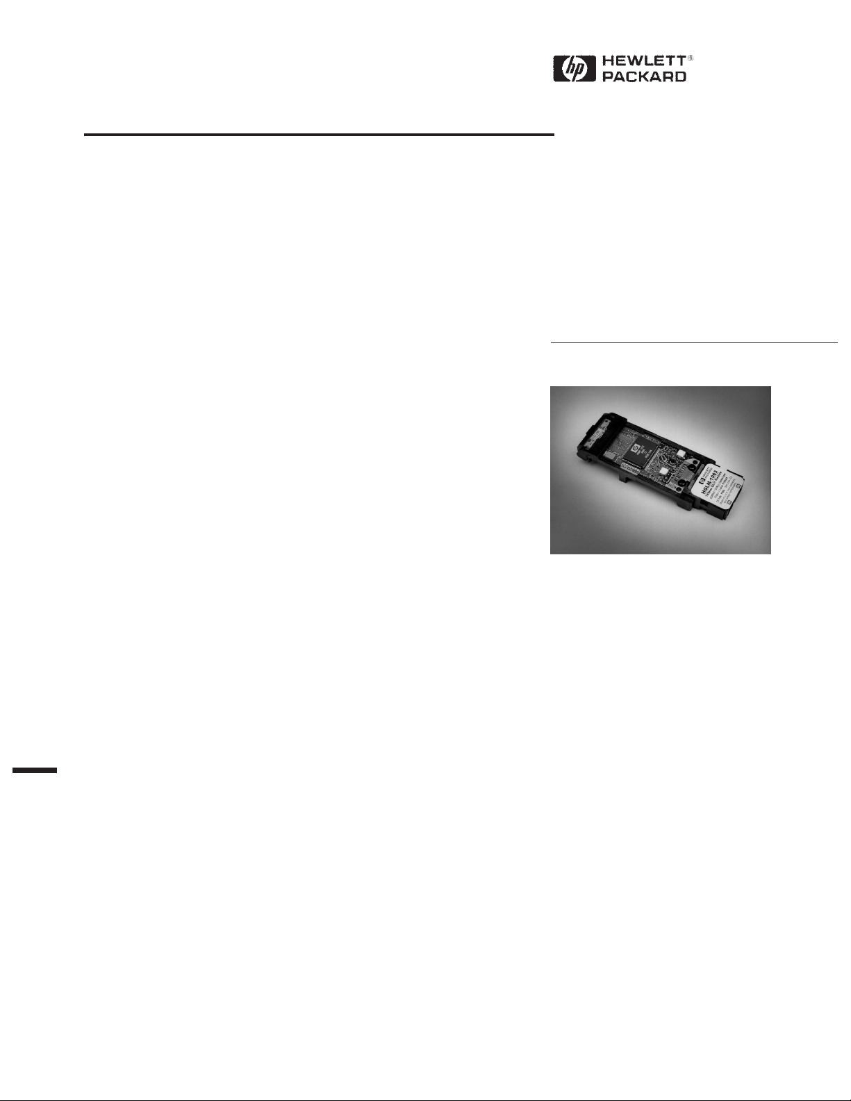
Fibre Channel GBaud Optical
Link Module
Technical Data
HGLM-1063
Features
• ANSI X3.230-1994 Fibre
Channel Standard
Compatible (FC-0)
• FCSI-301-Rev 1.0 “GBaud
Link Module Specification”
Compatible
• Standard 20 Bit (1063 MBd),
TTL Interface
• Class I Laser Safety
Certified
• Single +5.0 V Power Supply
Applications
• Mass Storage System I/O
Channel
• Computer System I/O
Channel
• High Speed Peripheral
Interface
Description
The HGLM-1063 Gigabaud
Optical Link Module, provides a
complete Fibre Channel FC-0
layer solution. The module meets
the requirements of the 100-M5-
SL-I physical link as defined by
the American National Standards
Institute (ANSI) X3.230-1994
Fibre Channel standard. The
HGLM-1063 is also compatible
with the Fibre Channel Systems
Initiative (FCSI) document
#FCSI-301-Rev 1.0 “Gigabaud
Optical Link Module”
specification.
The HGLM-1063 transmits and
receives 8b/10b encoded,
parallel, data in the 20 bit wide
format defined by the FCSI-301
document. The 20 bit wide data is
transmitted at 100MB/sec over a
serial fiber link and has the
capability to receive data at
100 MB/sec simultaneously. With
overhead, this translates to a
serial line rate of 1062.5 MBaud
transmitting and 1062.5 MBaud
receiving. The serial data link
uses a 780 nm laser transmitter
and photodiode. The optimum
fiber is 50/125 µm multimode
fiber (62.5/125 µm multimode
fiber can be used with degraded
performance) and attaches to the
HGLM-1063 via a duplex SC
connector.
As specified in the Fibre Channel
Standard, the HGLM-1063 is a
Class 1 laser safe device; the
transmitted optical signal shuts
down in the case of an open fiber
condition after a specific time
interval. The HGLM-1063
accomplishes this by monitoring
the transmitted optical power
levels, and the received optical
signal.
The HGLM-1063 is intended for
use in building adapter cards (or
equivalent devices) as shown in
Figure 1. The HGLM-1063 provides complete FC-0 functionality.
The HPFC-5000 provides the
FC-1 through FC-4 functions and
interfaces directly to the HGLM-
1063. Finally, a bus gasket is
used to connect the HPFC-5000
to the specific system bus in use.
This block diagram is meant only
to illustrate the basic Fibre
Channel functionality.
For proper operation, it is
necessary to connect the HGLM1063 to another HGLM-1063 (or
equivalent) in a full duplex
configuration as depicted in
Figure 3. This ensures proper
operation of the Open Fiber
Control circuitry and allows
proper link startup and
synchronization.
726
5964-6638E (4/96)

HPFC-5000
TACHYON
SYSTEM BUS
Figure 1. Example System Adapter Card, Block Diagram (Simplified).
BUS GASKET
HGLM-1063
GIGABAUD OPTICAL
LINK MODULE
Tx
FIBER
Rx
Functional Description
A simplified block diagram of the
HGLM-1063 module is shown in
Figure 2. This block diagram
shows the 5 key elements of the
module. These are the Transmitter I.C., the Laser Diode Assembly,
the Receiver I.C., the photodiode
assembly, and the Open Fiber
Control circuit. The high level of
integration on the HGLM-1063 is
apparent from this block
diagram. Pin assignments and
signal definitions are given on
pages 6 and 7.
In general, the HGLM-1063
utilizes a user provided Transmit
Byte Clock (TBC) of 53.125 MHz
to transmit two 8b/10b encoded
data bytes, simultaneously, by
creating a serial data stream of
1062.5 MBd and modulating a
780 nm laser diode with it. The
20 bit wide (two encoded bytes)
data input is provided to the
module through the 80 pin connector in standard TTL format.
Similarly, the HGLM-1063
receives 780 nm optical signals at
a data rate of 1062.5 MBd,
deserializes this data stream to
recover the two encoded data
bytes and provides this 20 bit
wide standard TTL data to the
receiving system via the 80 pin
connector. The receiver also
recovers the byte rate clock for
use in clocking the received 20
bit wide parallel data.
Link Acquisition and Power Up
The following discussion assumes
the HGLM-1063 is connected in a
full duplex point to point link as
shown in Figure 3. When initially
applying power to the HGLM1063, the Transmit Byte Clock
must start no later than 5 msec
after the +5 volt supply reaches
the +4 volt level. If this requirement is not met, the Open Fiber
Control (OFC) circuit may stick
in a nonfunctional state. If this
should happen, the OFC can be
put into a functional state by
holding the Enable Wrap
(EWRAP) line high for 10.5
seconds. Once the TBC is
running, and the module is
properly powered up, the following sequence should be followed
to bring the link into full
synchronization and ready to
transmit data:
1. Both Link Unusable lines will
be driven high, by the OFC,
indicating neither receiver is
detecting a signal from the link.
2. Drive the Transmit Data lines,
Tx[00:19] to a
01010101010101010101.
3. Drive the input control lines as
follows:
• Enable Wrap: low
• Tx_SI: low
• Enable Comma Detect: high
• -Lock to Reference: high
4. Assuming the link is properly
connected, and both link ends are
in the same state of readiness, the
lasers will turn on in 10.1
seconds. This will be indicated by
the Link Unusable lines going
low. This transition indicates the
OFC is operational and in
control.
5. Once the lasers have come on,
and Link Unusable is observed to
transition low, bring -Lock to
Reference low for at least
500 µsec. This forces the module
to frequency lock to the Transmit
Byte Clock.
727
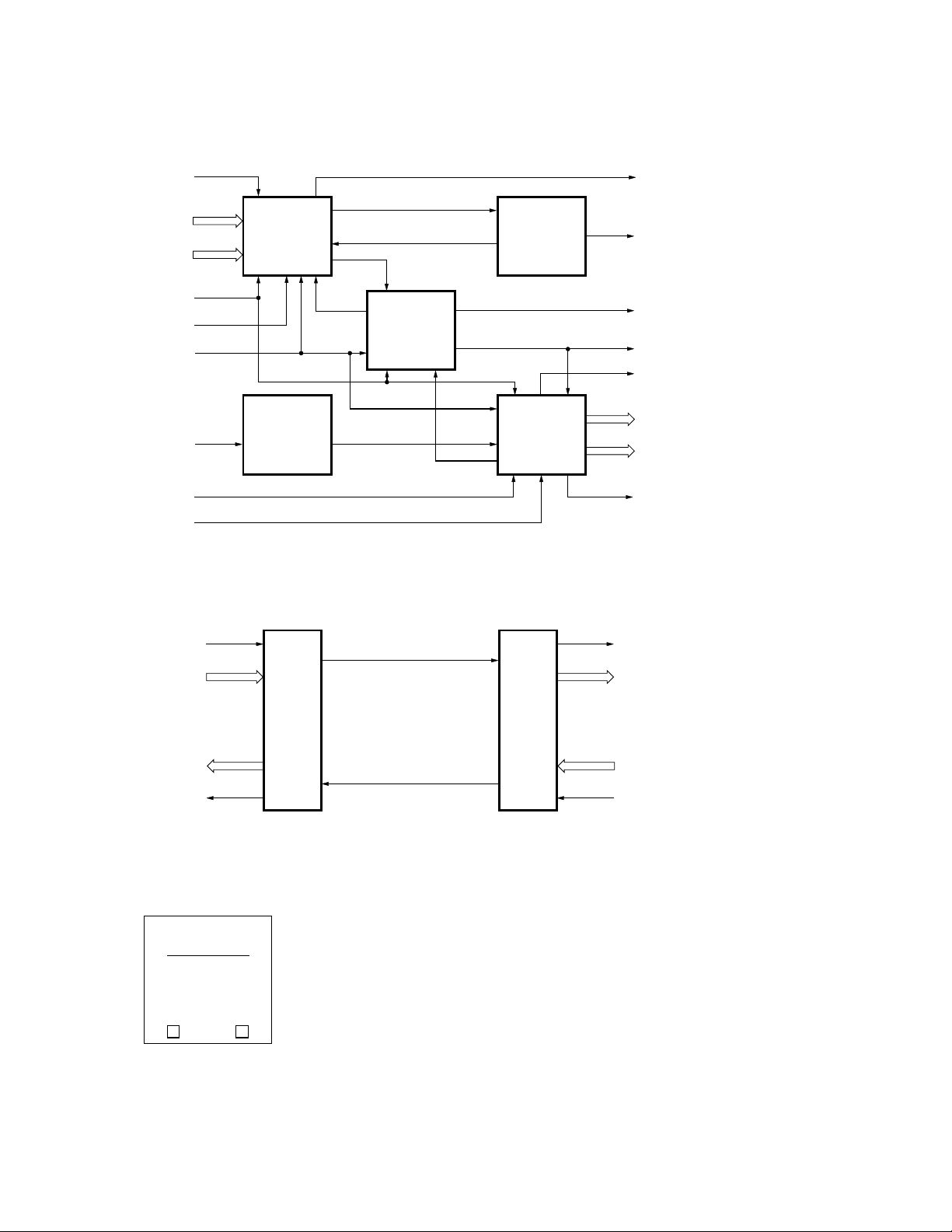
± SERIAL DATA IN
± SERIAL DATA OUT
DATA BYTE 0
Tx[00:09]
DATA BYTE 1
Tx[10:19]
EWRAP
Tx_SI
TBC
FIBER INPUT
EN_CDET
-LCK_REF
HDMP-1512
TRANSMITTER
I.C.
PHOTODIODE
ASSEMBLY
FAULT
-LZON
OPEN FIBER
CONTROL
Figure 2. HGLM-1063 Functional Block Diagram.
CLOCK (TBC)
Tx
ENCODED DATA
FIBER PATH A
I.C.
LOL A, B
LASER DIODE
ASSEMBLY
HDMP-1514
RECEIVER
I.C.
Rx
FIBER OUTPUT
FAULT
L_UNUSE
RBC[0:1]
DATA BYTE 0
Rx[00:09]
DATA BYTE 1
Rx[10:19]
COM_DET
CLOCK (RBC[0:1])
ENCODED DATA
HGLM1 HGLM2
ENCODED DATA
CLOCK (RBC[0:1])
Rx
Figure 3. Full Duplex Point to Point Link.
H
HGLM-1063
780 nm GLM Module
CDRH21 CFR(J) Compilant
Class 1 Laser Product
09 Nov. 1995 San Jose, CA
Made in U.S.A. from domestic
and foreign components.
Rx Tx
Figure 4. Typical HGLM-1063 Label.
FIBER PATH B
Tx
ENCODED DATA
CLOCK (TBC)
728

6. After holding -Lock to
Reference low for 500 µsec it
should then be driven high. This
causes the module to phase and
frequency lock onto the incoming
data stream within 2500 bit times
(2.4 µsec).
7. After 2500 bit times, the
modules should be in bit synchronization, but not yet byte
synchronization. The Receive
Byte Clock (RBC0) should be
running at 53.125 MHz.
8. Finally, drive the data lines
Tx[00:19] with a K28.5 (comma
or byte sync) character. Upon
detection of this character, the
receiver will drive the Comma
Detect line high, the clocks will
align to the byte boundary, and
the receive data lines (Rx[00:19])
will have valid data. The link is
now ready for data transmission.
TX_SI Operation
In normal operation, pin Tx_SI
should be held low. In this mode,
the data at Tx[00:19] is serialized
and driven over the fiber optic
link. With pin Tx_SI driven high,
however, the data at Tx[00:19] is
serialized and driven out the
± Serial Data Out lines and the
data applied to the ± Serial Data
In lines are driven over the fiber
optic link.
EWRAP Operation
To aid in link diagnostics, the
modules have the capability of
wrapping the local transmit data
electrically back to the local
deserializer. This feature is
enabled by driving the EWRAP
pin high. When enabled, EWRAP
causes the laser to turn off within
20 µsec. The OFC circuit goes
into its low duty cycle “on-off-on”
handshake mode. The link will
need to be stepped through the
synchronization procedure
outlined above to return to
normal operation after EWRAP is
brought low.
Enable Comma Detect
In the synchronization procedure
above, the Enable Comma Detect
(EN_CDET) signal is driven high
to allow the receiver to reset and
align its boundaries properly
when a K28.5 character is
transmitted. This line can be kept
in a high state and the receiver
will reset on every K28.5
character it detects. This feature
can be disabled, after initial
synchronization, by driving
Enable Comma Detect to a low
state.
Open Fiber Control
The purpose of the Open Fiber
Control (OFC) integrated circuit
is to ensure user safety. This
circuit uses the dual loss of light
signals from the receiver I.C. and
the laser Fault detection signal
from the transmitter I.C. to
determine if the laser and the
fiber link are properly connected
and functioning normally. Should
a Fault condition be determined,
all laser transmission is shut
down.
A safety interlock is provided by
the HGLM-1063 module. HGLM1063 modules (or equivalent)
must be connected in full pointto-point configuration as shown
in Figure 3 for proper operation.
The Open Fiber Control System
(OFCS) of the HGLM-1063
deactivates the laser signal
whenever there is an interruption
or loss of signal of either laser
drive circuit.
For example, in Figure 3, if Path
A is opened through a cut or
other physical damage to the
fiber, or if the fiber is discon-
nected at either the transmitting
port of HGLM1 or the receiving
port of HGLM2, the OFCS detects
the loss of signal. The Link
Unusable line of HGLM2 goes
high, signaling the system of an
open fiber condition. The OFCS
then shuts down the laser of
HGLM2. HGLM1 in turn detects
this loss of signal, raises its Link
Unusable line, and shuts down its
laser. The OFC pulses the laser of
HGLM2 at a very low duty cycle.
Simultaneously, the OFCS of
HGLM1 detects the low duty
cycle operation of HGLM2 and
places its laser in the same low
duty cycle pulsing mode. It takes
less than 2 msec to shut down all
laser transmission and results in a
safe (Class I) laser emission level
in Path A, the open path.
While Path A is still open,
HGLM1 launches a pulse
synchronously with the pulse it
receives on Path B from HGLM2.
However, HGLM2 receives no
pulse (because Path A is open)
and continues in an inactive
mode. HGLM2 will continue
launching “inquiry” pulses once
approximately every 10.1 seconds
along Path B.
After Path A is restored, HGLM2
will receive pulses along Path A,
synchronous with its transmit
pulses along Path B. A completed
link of Path A and Path B is
verified by both HGLM1 and
HGLM2. HGLM2 will verify its
link by deactivating its laser and
confirm that its receive signal
disappears. HGLM1 also
performs the same verification
check, deactivating its laser.
Once both HGLM modules have
729

deactivated their lasers, HGLM2
then activates its laser, sends a
signal to HGLM1 (which activates
its laser), which in turn sends a
confirming signal back to
HGLM2. This on-off-on handshake
confirms that the first synchronous pulse came from
another HGLM-1063, or
equivalent module, with an OFC
safety system. Once this
sequence is complete, the link
between HGLM1 and HGLM2
returns to normal operation, with
both in the active mode. The onoff-on timing is compatible with
the timing requirements of the
ANSI FC-PH specification for
Open Fibre Control timing of
100-M5-SL-I links. These timings
are defined as Decode 1, 2, and 3
and are given in the Timing
Specifications table later in this
document.
Laser Safety Compliance
The HGLM-1063 is designed and
certified as a Class 1 laser
product per 21 CFR (U.S. Code
of Federal Regulations),
Subchapter J. A Class 1 laser
product is safe for use and does
not pose a biological hazard if
used in accordance within the
data sheet limits and instructions.
CAUTION:
There are no user serviceable
parts nor any maintenance
required for the HGLM-1063.
All adjustments are made at
the factory before shipment to
our customers. Tampering
with, modifying or breaking
the preset trim pot seals will
result in voided product
warranty. It may also result in
improper operation of the
HGLM-1063 circuitry, and
possible overstress of the
laser source. Device degradation or product failure may
result.
Connection of the HGLM-1063
to a non-approved optical
source, operating above the
recommended absolute maximum conditions (especially
power supply) or operating
the HGLM-1063 in a manner
inconsistent with its design
and function may result in
hazardous radiation exposure
and may be considered an act
of modifying or manufacturing
a laser product. The person(s)
performing such an act is
required by law to recertify
and reidentify the laser
product under the provisions
of 21 CFR(Subchapter J).
Labeling
Each HGLM-1063 module is
labeled per 21 CFR
(Subchapter J), including the
actual date of manufacture
(Figure 4).
5.0
3.5
(0.138)
35.25
(1.388)
24.13
(0.950)
DIMENSIONS IN MILLIMETERS (INCHES).
Figure 5. HGLM-1063 Outline Drawing.
(0.197)
(2X)
74.27 (2.924)
63.53 (2.501)
730
30.8
(1.213)
37.8
(1.488)
2.5
φ
PIN
(0.098)
BOTTOM VIEW
28.35 (1.116)
27.0 (1.063)
4.8 (0.189)
RECEIVER
TRANSMITTER
2.5 mm DIAMOND PIN
2.0
φ
(0.079)
(2X)
1.25
(0.049)
11.0
(0.433)
2.0
(0.079)
11.5
(0.453)
25.4
(1.000)
28.0
(1.102)
30.0
(1.181)

SOCKET A01
ACCOMODATES
A PIN SPEC'D
φ 0.46 ± 0.05
φ
0.2 M A B M C M
4.8 MAX.
A
R1.6 TYP.
36.4 MIN.
30.2 MAX.
4.8
1.6 ± 0.25
φ 2.65 ± 0.08
φ
0.13 M A B M
C
24.5
MIN.
D
36.8 PITCH
32 ± 0.2
30
φ
0.1 M A D
OPTICAL
AXIS
B
NO ELECTRICAL TRACE
PLACEMENT
AXIS
28.85
MIN.
SOCKET A20
ACCOMODATES
A PIN SPEC'D
φ 0.46 ± 0.05
φ
0.2 M A B M C M
24.13
2.94
(2X)3.35 MIN.
63.53
(2X)64.27 MIN.
(2X)2.6 MIN.
37.2 MAX.
43.4 MIN.
7.5 MIN.
φ 2.65 ± 0.08
Figure 6. Host PCB Layout for Mounting the HGLM-1063.
HGLM-1063 Pin Assignments
Pin Name Pin Name Pin Name Pin Name
A01 +SO B01 -SO C01 gnd D01 +SI
A02 gnd B02 gnd C02 gnd D02 -SI
A03 V
CC
A04 TX[12] B04 TX[11] C04 TX[02] D04 TX[01]
A05 TX[14] B05 TX[13] C05 TX[04] D05 TX[03]
A06 TX[16] B06 TX[15] C06 TX[06] D06 TX[05]
A07 TX[18] B07 TX[17] C07 TX[08] D07 TX[07]
A08 gnd B08 TX[19] C08 TX[09] D08 gnd
A09 STROB_ID B09 gnd C09 gnd D09 V
A10 V
CC
A11 PAR_ID[1] B11 rsv C11 TX_SI D11 PAR_ID[0]
A12 RBC[0] B12 EWRAP C12 COM_DET D12 V
A13 V
CC
A14 gnd B14 RX[10] C14 RX[00] D14 gnd
A15 RX[12] B15 RX[11] C15 RX[02] D15 RX[01]
A16 RX[14] B16 RX[13] C16 RX[04] D16 RX[03]
A17 RX[16] B17 RX[15] C17 RX[06] D17 RX[05]
A18 RX[18] B18 RX[17] C18 RX[08] D18 RX[07]
A19 V
CC
A20 EN_CDET B20 gnd C20 gnd D20 -LCK_REF
B03 TX[10] C03 TX[00] D03 V
CC
CC
B10 L_UNUSE C10 FAULT D10 TBC
CC
B13 gnd C13 rsv D13 RBC[1]
B19 RX[19] C19 RX[09] D19 V
CC
731

HGLM-1063 Signal Definitions
Logic
Symbol Signal Name I/O Level Description
TX[00:19] Transmit Data Input TTL The 20-bit parallel transmit data to be serialized
and sent to the transmitter.
TBC Transmit Byte Clock Input TTL Used to operate the state machines, derive the
20X serial clocks, and latch TX[00:19].
EWRAP Enable Wrap/Enable Input TTL Causes the serialized transmit data to electrically
STROP_ID wrap back to the deserializer and disables the
laser output.
-LCKREF Lock to Reference Input TTL Causes the PLL to lock to TBC.
TX_SI Transmit SI Input TTL Selects the serial data mode.
EN_CDET Enable Comma Input TTL Enables the comma detection circuitry to
Detect/STROB_ID clock establish byte synchronization on the next
comma that is received.
± SI Serial Data In Input PECL A pair of differential signals for transmission of
serial data.
RX[00:19] Receive Data Output TTL The 20 bit decoded received data from the
receiver.
RBC[0] Receive Byte Clock 0 Output TTL Used by the system to latch RX[00:19].
RBC[1] Receive Byte Clock 1 Output TTL Not normally used.
COM_DET Comma Detect Output TTL Indicates byte synchronization has occurred.
L_UNUSE Link Unusable Output TTL Indicates the link is currently not usable.
FAULT Fault Output TTL Indicates an electrical fault has been detected
and turns the laser output off.
± SO Serial Data Out Output PECL A pair of high speed differential signals
representing the serialized data.
PAR_ID Parallel ID Output TTL A 2 bit identification of the link rate.
STROB_ID Strobed ID Output TTL Optional output used to access the serial
Strobed ID information. Not active.
rsv Reserved Reserved for future use.
Absolute Maximum Ratings
TC = 25°C, except as specified. Operation in excess of any one of these conditions may result in permanent
damage to this device.
Symbol Parameter Units Min. Max.
732
V
CC
V
IN,TTL
I
O,TTL
T
stg
T
OP
RHop Relative Humidity Operating % 8 80
RHst Relative Humidity Storage % 5 95
Supply Voltage V -0.5 6.0
TTL Data Input Voltage V -0.7 VCC + 0.7
TTL Output Source Current mA 13
Storage Temperature °C -40 +75
Ambient Operating Temperature °C 0 +60

Transmit Byte Clock Requirements
TA = 10°C to +50°C, VCC = 4.5 V to 5.5 V
Symbol Parameter Unit Min. Typ. Max.
f Nominal Frequency MHz 53.119 53.125 53.131
F
tol
Frequency Tolerance (for Fibre Channel Compliance) ppm -100 +100
Symm Symmetry (Duty Cycle) % 40 60
Jpe Positive Edge Jitter ns 0.5
t
r
t
f
Rise Time, 20% to 80% nsec 4
Fall Time, 20% to 80% nsec 4
DC Electrical Specifications
TA = 10°C to +50°C, VCC = 4.5 V to 5.5 V
Symbol Parameter Unit Min. Typ. Max.
V
IH,TTL
V
IL,TTL
V
OH,TTL
V
OL,TTL
I
CC
V
CC,noise
TTL Input High Voltage Level, Guaranteed High Signal for
All Inputs, IIH = 100 µAV25
TTL Input Low Voltage Level, Guaranteed Low Signal for
All Inputs, IIL = -1 mA V 0 0.8
TTL Output High Voltage Level, IOH = 1 mA V 2.4 5
TTL Output Low Voltage Level, IOL = -1 mA V 0 0.6
VCC Supply Current mA 1200
Peak to Peak Noise and Ripple Allowed on the VCC Input mV 100
AC Electrical Specifications
TA = 10°C to +50°C, VCC = 4.5 V to 5.5 V
Symbol Parameter Units Min. Typ. Max.
t
r,TTLin
t
f,TTLin
t
r,TTLout
t
f,TTLout
t
r,RBC
t
f,RBC
t
r, BLL
t
f,BLL
VSWR
VSWR
V
IP,H50
V
OP,BLL
o,BLL
Input TTL Rise Time, 20% to 80% nsec 2
Input TTL Fall Time, 20% to 80% nsec 2
Output TTL Rise Time, 20% to 80%, 15 pF Load nsec 2 4
Output TTL Fall Time, 20% to 80%, 15 pF Load nsec 2 4
Receive Byte Clock Rise Time, 0.8 V to 2.0 V, 15 pF Load nsec 1.5 3.0
Receive Byte Clock Fall Time, 2.0 V to 0.8 V, 15 pF Load nsec 1.5 2.4
BLL Rise Time, AC Coupled, 25 Ω Source and Load, 20% to 80% psec 150 350
BLL Fall Time, AC Coupled, 25 Ω Source and Load, 20% to 80% psec 150 350
H50 Input VSWR, AC Coupled, 50 Ω Source and Load 2.0
i,H50
BLL Output VSWR, AC Coupled, 50 Ω Source and Load 2.0
Input Peak-To-Peak Differential Voltage, AC Coupled, 50 Ω Load mV 50 1200 2000
BLL Output Peak-To-Peak Differential Voltage, AC Coupled, mV 1200 1400 2000
50 Ω Load
733

Timing Specifications
TA = 10°C to +50°C, VCC = 4.5 V to 5.5 V
Symbol Parameter Units Min. Typ. Max.
t
Dcd_1
t
Dcd_2
t
Dcd_3
Decode 1 Time µsec 154
Decode 2 Time µsec 617
Decode 3 Time µsec 154
Transmitter
t
s
t
h
Transmit Data Setup Time nsec 2.0
Transmit Data Hold Time nsec 3.3
Receiver
t
s
t
h
Receive Data Setup Time nsec 2.5
Receive Data Hold Time nsec 6.0
Optical Specifications
TA = 10°C to +50°C, VCC = 4.5 V to 5.5 V
Symbol Parameter Units Min. Typ. Max.
f
op
OPB Optical Power Budget dB 6 8
PT Transmitter Launched Optical Power, Average dBm -5.0 -2.5 1.3
P
Rx
RL Receiver Return Loss dB 12
λ Receiver Operating Wavelength nm 770 780 850
λ
C
∆λ Transmitter Spectral Width, RMS nm 4
RIN
DJ Transmitter Deterministic Jitter, peak-peak % 20
Serial Baud Rate Mbaud 1062.38 1062.5 1062.62
Optical Extinction Ratio dB 6
Receiver Input Power, Average, BER = 10
-12
dBm -13.0 1.3
Transmitter Spectral Center Wavelength nm 770 790 795
Transmitter Relative Intensity Noise dB/Hz -116
12
Transmitter Eye Opening, peak-peak, BER = 1E-12 % 57
734

TBC
ts
th
Tx[00:19]
DATADATA DATA DATA DATA
Figure 7. Transmit Byte Clock and Data Timing Relationships.
COM_DET
Rx[00:19]
RBC0
K28.5 DATA DATA
ts
th
18.8 ns
ts th
Figure 8. Receive Timing Relationships.
735
 Loading...