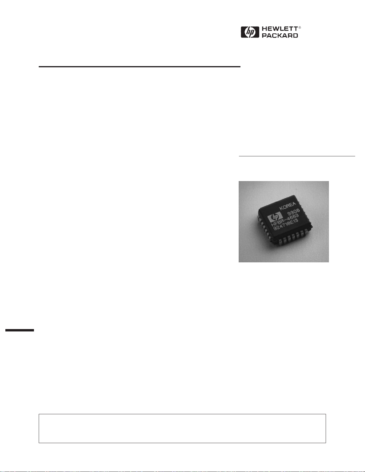
HP HFBR-4663 Datasheet

Single Chip 10BASE-FL
Transceiver
Technical Data
HFBR-4663
General Description
The HFBR-4663 Single Chip
10BASE-FL Transceiver is a
highly integrated circuit for IEEE
802.3 10Base-FL transceivers.
This product, when used with
HP’s fiber-optic transmitters and
receivers (HFBR-14X4 and
HFBR-2416), ensures
compliance to the 10Base-FL
Standard with a minimum
number of external components
and board space.
The HFBR-4663 offers a standard
IEEE 802.3 AU interface that
allows it to be directly connected
to industry standard manchester
encoder/decoder chips or an AUI
connector. The fiber-optic LED
driver offers a current drive
output that directly drives the
HFBR-14X4 transmitter. The data
quantizer section of the HFBR4663 is directly compatible with
the output of the HFBR-24X6
fiber-optic receiver and is capable
of accepting input signals as low
as 2 mVp-p with a 55 dB dynamic
range.
The transmitter automatically
inserts 1 MHz signal during idle
time and removes this signal on
reception. Low light is continuously monitored for both activity
as well as power level. Five LED
status indicators monitor error
conditions as well as transmissions, receptions, and collisions.
Features
• Single Chip Solution for
10BASE-FL Internal or
External Medium
Attachment Units (MAUs)
• Specifically Designed for Use
with HFBR-14X4 and HFBR24X6 Fiber-optic
Transmitters and Receivers
• Incorporates an AU Interface
• Highly Stable Data Quantizer
with 55 dB Input Dynamic
Range
• Input Sensitivity as Low
as 2 mV
P-P
• Current Driven Fiber Optic
LED Driver for Accurate
Launch Power
• Single +5 Volt Supply
• No Crystal or Clock
Required
• Five Network Status LED
Outputs
• Available in 28 Pin PCC
Package
• Semi-Standard Option
Available
CAUTION: The small junction sizes inherent to the design of this component increase the component's susceptibility to damage from electrostatic discharge (ESD). It is advised that normal static precautions be taken in
handling and assembly of this component to prevent damage and/or degradation which may be induced by
ESD.
5965-8597E (5/97)
77

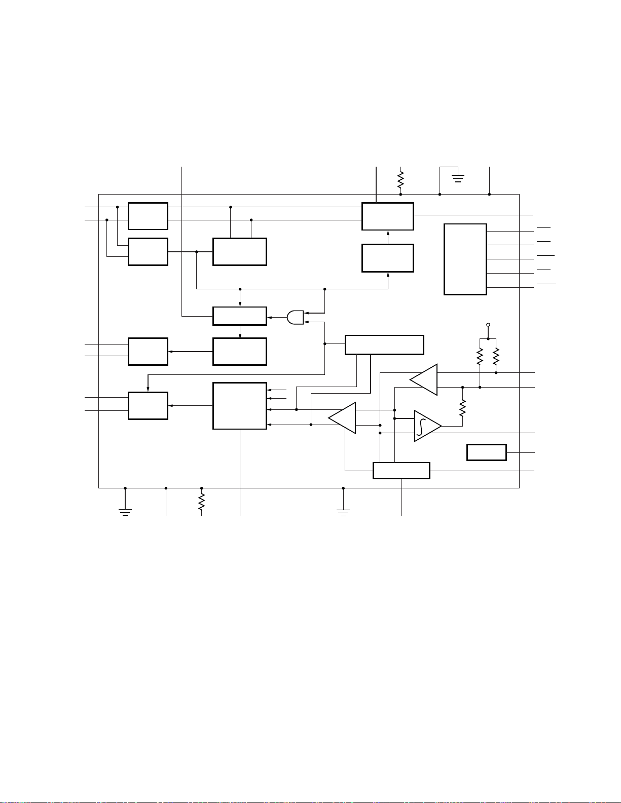
Block Diagram
SQEN/JABD
VCCTx
(+5 V)
+5 V
RTSET
GND
AV
CC
Tx+
Tx-
COL+
COL-
Rx+
Rx-
AUI
RECEIVER
Tx
SQUELCH
AUI
DRIVER
AUI
DRIVER
1 MHz IDLE
SIGNAL
SQE
10 MHz GATED
OSCILLATOR
LOOPBACK
MUX
Tx
Rx
FIBER OPTIC
DRIVER
JABBER
RECEIVE SQUELCH
CMP
LED
LINK DETECT
AMP
LED
DRIVERS
BIAS
V
REF
TxOUT
XMT
RCV
CLSN
JAB
LMON
VIN+
VIN-
V
DC
V
REF
V
THADJ
78
GND
V
CC
(+5 V)
+5 V
RRSET
LBDIS AGND
C
TIMER

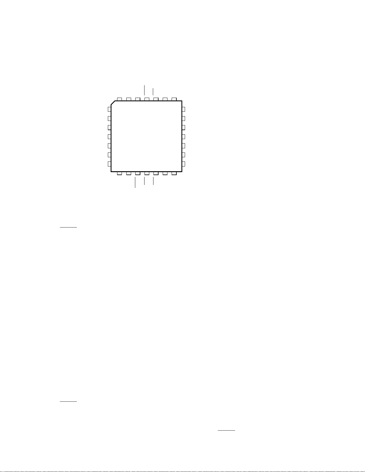
Pin Connection
28 – PIN PCC Q – 28
SQEN/JABD
Rx+
Rx-
LBDIS
V
CC
Tx+
Tx-
TIMER
C
COL-
COL+
CLSN
JAB
4321282726
5
6
7
8
9
10
11
12 13 14 15 16 17 18
XMT
RCV
RRSET
TOP VIEW
LMON
RTSET
AVCCV
Tx
CC
V
IN+
25
24
23
22
21
20
19
TxOUT
V
IN-
AGND
V
THADJ
V
REF
V
DC
GND
GND
Pin Description
Pin Name Function
1 CLSN Indicates that a collision is taking place. Active low LED driver, open collector.
Event is extended with internal timer for visibility.
2 COL+ Gated 10 MHz oscillation used to indicate a collision, SQE test, or jabber.
3 COL- Balanced differential line driver outputs that meet AUI specifications.
4C
TIMER
5 SQEN/JABD SQE Test Enable, jabber Disable. When tied low, SQE test is disabled, when tied
6 Rx+ Manchester encoded receive data output to the local device. Balanced
7 Rx- differential line driver outputs that meet AUI specifications.
8 LBDIS Loopback Disable. When this pin is tied to VCC, the AUI transmit pair data is not
9V
CC
10 Tx+ Balanced differential line receiver inputs that meet AUI specifications. These
11 Tx- inputs may be transformer or capacitively coupled. The Tx input pins are
12 RTSET Sets the current driven output of the transmitter.
13 RRSET A 1% 61.9 kΩ resistor tied from this pin to VCC sets the biasing currents for
14 LMON Link Monitor “Low Light” LED status output. This pin is pulled low when the
A capacitor from this pin to VCC determines the Link Monitor response time.
high SQE test is enabled. When tied to 2.0 V both SQE test and jabber are
disabled.
looped back to the AUI receive pair, and collision is disabled. When this pin is
tied to GND (normal operation) or left floating, the AUI transmit pair data is
looped back to the AUI receiver pair, except during collision.
+5 V power input.
internally DC biased for AC coupling.
internal nodes.
voltage on the VIN+, VIN- inputs exceed the minimum threshold set by the V
pin, and there are transitions on VIN+, VIN- indicating an idle signal or active
data. If either the voltage on the VIN+, VIN- inputs fall below the minimum
threshold or transitions cease on VIN+, VIN-, LMON will go high. Active low LED
driver, open collector.
THADJ
79

Pin Description (cont.)
Pin Name Function
1 5 XMT Indicates that transmission is taking place. Active low LED driver, open
collector. Event is extended with internal timer for visibility.
1 6 RCV Indicates that the transceiver is receiving a frame from the optical input. Active
low LED driver, open collector. Event is extended with internal timer for
visibility.
17 VCCTx +5 V supply for fiber optic LED driver.
18 TxOUT Fiber optic LED driver output.
19 GND Ground Reference.
20 GND Ground Reference.
21 V
22 V
23 V
DC
REF
THADJ
24 AGND Analog Filtered Ground.
25 VIN- This input pin should be capacitively coupled to the input source or to filtered
An external capacitor on this pin integrates an error signal which nulls the
offset of the input amplifier. If the DC feedback loop is not being used, this pin
should be connected to V
REF
.
A 2.5 V reference with respect to GND.
This input pin sets the link monitor threshold.
AVCC. (The input resistance is approximately 1.3 kΩ.)
26 VIN+ This input pin should be capacitively coupled to the input source or to filtered
AVCC. (The input resistance is approximately 1.3 kΩ.)
27 AV
CC
Analog Filtered +5 V.
28 JAB Jabber network status LED. When in the jabber state, this pin will be low and
the transmitter will be disabled. In the jabber “OK” state this pin will be high.
Active low LED, open collector.
Absolute Maximum Ratings
[1]
Parameter Symbol Min. Max. Units
Storage Temperature T
Operating Temperature T
S
A
-65 +150 C
070C
Lead Soldering Cycle 260 C
Temperature
Lead Soldering Cycle Time 10 sec
Power Supply Voltage Range V
CC
-0.3 6.0 V
Input Voltage Range Digital Inputs (SQEN, LBDIS) -0.3 6.0 V
Tx+, Tx-, VIN+, VIN- -0.3 6.0 V
Input Current RRSET, RTSET, JAB, CLSN, 60 mA
XMT, RCV, LMON
Output Current TxOUT 70 mA
80

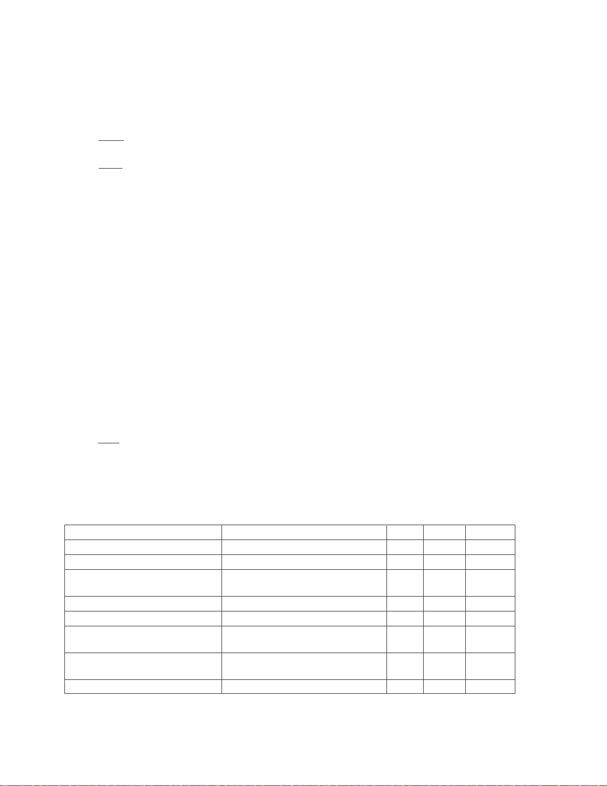
Operating Conditions
Parameter Min. Typ. Max. Units
Supply Voltage (VCC) 4.75 5.0 5.25 V
LED on Current 10 mA
RRSET 61.9 k ± 1% Ω
RTSET 140 ± 1% Ω
Electrical Characteristics
[4]
[2,3]
220 mA
0.8 V
-200 10 +200 µA
567mV
Unless otherwise specified, TA = 0°C to 70°C, VCC = VCCTx = 5 V ± 5%
Parameter Condition Min. Typ. Max. Units
Power Supply Current ICC:V
= 5 V, RTSET = 140 Ω
CC
While Transmitting
LED Drivers: V
CC
Transmit Peak Output Current
[6]
IOL = 10 mA
RTSET = 140 Ω 47 52 57 mA
[5]
Transmit Squelch Voltage Level -300 -250 -200 mV
(Tx+, Tx-)
Differential Output Voltage ± 550 ± 1200 mV
(Rx± , COL± )
Common Mode Output Voltage 4.0 V
(Rx± , COL± )
Differential Output Voltage ± 40 mV
Imbalance (Rx± , COL± )
SQE/JABD SQE Test Disable 0.3 V
Both Disabled 1.5 VCC - 2 V
Both Enabled VCC - 0.5 V
LBDIS Threshold Disabled VCC - 0.1 V
Enabled 1 V
Common Mode Voltage (Tx+, Tx-) 3.5 V
Common Mode Voltage (VIN+, VIN-) 1.65 V
Reference Voltage 2.35 2.45 2.55 V
V
Output Source Current 5 mA
REF
Amplifier Gain 100 V/V
Input Signal Range 2 1600 mV
External Voltage at V
Set V
TH
Input Offset VDC = V
to 0.5 2.7 V
THADJ
(DC loop active) 3 mV
REF
Input Referred Noise 50 MHz BW 25 µV
Input Resistance VIN+, VIN- 0.8 1.3 2.0 kΩ
Input Bias Current of V
Input Threshold Voltage V
THADJ
THADJ
= V
REF
[7]
Hysteresis 20 %
P-P
P-P
81
 Loading...