

Page 1

TM 11-6625-2820-14&P
TECHNICAL MANUAL
OPERATOR'S, ORGANIZATIONAL, DIRECT SUPPORT, AND
GENERAL SUPPORT MAINTENANCE MANUAL
INCLUDING REPAIR PARTS AND SPECIAL TOOLS LISTS
FOR
SIGNAL GENERATOR SG-735 / URM-165
(HEWLETT-PACKARD MODEL 8616A)
(NSN 6625-00-254-6671)
HEADQUARTERS, DEPARTMENT OF THE ARMY
JULY 1977
Page 2

d-
●
*
Page 3

TM 11-6625-2820-14&P
C2
CHANGE
HEADQUARTERS
DEPARTMENT OF THE ARMY
No. 2
Washington, DC, 1 January 1988
OPERATOR’S, ORGANIZATIONAL, DIRECT SUPPORT
AND GENERAL SUPPORT MAINTENANCE MANUAL
INCLUDING REPAIR PARTS AND SPECIAL TOOLS LISTS
(INCLUDING DEPOT MAINTENANCE REPAIR PARTS AND SPECIAL TOOLS)
FOR
SIGNAL GENERATOR SG-735/URM-165
(HEWLETT-PACKARD MODEL 8616A)
(NSN 6625-00-254-6671)
TM 11-6625-2820-14&P, 22 July 1977, is changed as follows:
Remove old pages and insert new pages as indicated below. New or changed material is indicated by a vertical bar
1.
in the margin of the page. Added or revised illustrations are indicated by a vertical bar adjacent to the identification
number.
Remove pages
Insert pages
iii and l-O . . . . . . . . . . . . . . . . . . . . . . . . . . . . . . . . . . ..iii and l-O
5-17 and 5-18 . . . . . . . . . . . . . . . . . . . . . . . . . . . . . . . . ..5-17 and 5-18
2. File this change sheet in the front of the publication for reference purposes.
Distribution authorized to the Department and DOD
for official use or for administration or operational purposes. This determination
was made on 1 October 1967. Other requests for this document will be referred
to Commander, US Army Communications-Electronics Command and Fort
Monmouth, ATTN: AMSE1-ME-P, Fort Monmouth, NJ 07703-5000.
contractors only
DESTRUCTION NOTICE – Destroy by any method that will prevent disclosure of
contents or reconstruction of the document.
Page 4

By Order of the Secretary of the Army:
Official:
R.L. DILWORTH
Brigadier General, United States Army
The Adjutant General
DISTRIBUTION:
To
be distributed in accordance with DA Form 12-36 literature
requirements for SG-735/URM-165.
CARL E. VUONO
General, United States Army
Chief of Staff
Page 5

TM 1 1-6425-2820-14&P
Cl
CHANGE
No. 1
HEADQUARTERS
DEPARTMENT OF THE ARMY
WASHINGTON, DC, 11 October 1978
Operator's, Organizational, Direct Support, and
General Support Maintenance Manual
Including Repair Parts and Special Tools Lists
(Including Depot Maintenance Repair Parts and Special Tools)
For
SIGNAL GENERATOR SG-735/URM-165
(HEWLETT-PACKARD MODEL 8616A)
(NSN 6626-00-254-6671)
This Changes is current as of 16 June 1978.
TM 11-6625-2820-14&P, 22 July 1977, is changed as follows:
1. The title is changed to read as shown above.
2. Remove old pages and insert new pages as indicated below.
3. New or changed material is indicated by a vertical bar in the margin of the page.
Remove Pages
i. ii, and iii
6-9 through 6-12
111-3 and III-4
IV-1 and IV-2 (unnumbered)
4.
File this change sheet in front of the publication for reference purposes.
Insert Pages
i through iv
6-9
111-3 and III-4
IV-1 through IV-31
Page 6

TM 11-6625-2820-14&P
By Order of the Secretary of the Army:
Official:
J.C. PENNINGTON
Brigadier General, United States Army
The Adjutant General
Distribution:
Active Army:
TSG (1)
USAARENBD (1)
USAINSCOM (2)
TRADOC (2)
DARCOM {2)
TECOM (2)
OS MAJ COMD (2)
USACC (2)
HISA (Ft Monmouth) (26)
Armies (1)
USASIGS (10)
Svc Colleges(1)
Ft Carson (5)
Ft Gillem (10)
Ft Huachuca (5)
Ft Richardson (CERCOM Ofc) (1)
WSMR(l]
USAERDAA (l)
USAERDAW (1)
Army Dep (1) except
LBAD (10)
SAAD (30)
SHAD (3)
(14)
TOAD
USA Dep (1)
Sig Sec USA Dep (1)
Units Org Under Fol TOE:
29-134
29-136
(1 cy each unit)
29-207
29-610
(2
copies each
unit)
BERNARD W. ROGERS
General, United States Army
Chief of Staff
ARNG:
None
USAR:
None
For explanation of abbreviations used, see AR 310-50.
U.S. GOVERNMENT PRINTING OFFICE: 1979-603-028/596
Page 7

This manual contains copyright material reproduced by permission of the Hewlett-Packard Company.
TM 11-6625-2820-14&P
ECHNICAL MANUAL
T
No. 11-6625-2820-14&P
OPERATOR’S, ORGANIZATIONAL, DIRECT SUPPORT, AND
GENERAL SUPPORT MAINTENANCE MANUAL
INCLUDING REPAIR PARTS AND SPECIAL TOOLS LISTS
(INCLUDING DEPOT MAINTENANCE REPAIR
SIGNAL GENERATOR SG-735/URM-165
HEADQUARTERS
DEPARTMENT OF THE ARMY
WASHINGTON, DC, 22 July 1977
PARTS AND SPECIAL TOOLS)
FOR
(HEWLETT-PACKARD MODEL 8616A)
( NSN 6625-00-254-6671 )
REPORTING OF ERRORS
You can improve this manual by recommending improvements using DA
Form 2028-2 located in the back of the manual. Simply tear out the self addressed form, fill it out as shown on the sample, fold it where shown, and drop
it in the mail.
If there are no blank DA Forms 2028-2 in the back of your manual, use the
standard DA Form 2028 (Recommended Changes to Publications and Blank
Forms) and forward to the Commander, US Army Communications and Electronics Materiel Readiness Command, ATTN: DRSEL-ME-MQ, Fort Monmouth, NJ 07703.
In either case a reply will be furnished direct to you.
This manual is an authentication of the manufacturer’s commercial literature which, through usage, has been
found to cover the data required to operate and maintain this equipment. Since the manual was not prepared
in accordance with military specifications, the format has not been structured to consider levels of maintenance.
Change 1 i
Page 8

TM 11-6625-2820-14&P
SECTION
0 INTRODUCTION . . . . . . . . . . . . . . . . .
I GENERAL INFORMATION . . . . . . . .
1-1.
Introduction . . . . . . . . . . . . . . . .
1-6.
Supplementary Instruments . .
Instrument Options . . . . . . . . . .
1-9.
1-11. Instrument Identification. . . . .
1-13. Klystron Warranty Claim Sheet
II INSTALLATION . . . . . . . . . . . . . . . . . .
2-1. Incoming Inspection. . . . . . . . . .
Installation . . . . . . . . . . . . . . . . .
2-3.
2-6. Conversion to Rack Mount. . .
2-7.
2-9.
Air Filter Inspection . . . . . . . .
Power Requirement . . . . . . . . . .
2-11. Three Conductor Power Cable. .
2-14. Repackaging for Shipment . . . .
III OPERATION . . . . . . . . . . . . . . . . . . . . .
3-1. Introduction . . . . . . . . . . . . . . . .
3-3. Controls and Indicators . . . . . . .
3-5. Operating Procedures. . . . . . . . .
3-7.
Stabilized Source . . . . . . . . . . . . .
IV PRINCIPLES OF OPERATION . . . . .
4-1. Introduction . . . . . . . . . . . . . . . .
4-3. RF Oscillator . . . . . . . . . . . . . . . .
4-6. Pin Diode Modulator . . . . . . . . .
4-16. Modulation Circuits. . . . . . . . . .
4-18.
4-20.
4-22.
4-25.
ExternalPulse . . . . . . . . . . . .
Internal Square Wave. . . . . . .
Extemal AM . . . . . . . . . . . . . .
Internal Meter and Automatic
Level Control (ALC) . . . . . . . .
4-36. External Leveling . . . . . . . . . .
4-37. Regulated Power Supply. . . . . .
V MAINTENANCE . . . . . . . . . . . . . . . . . .
Introduction . . . . . . . . . . . . . . . .
5-1.
Test Instruments Required. . . .
5-3.
Periodic Maintenance. . . . . . . . .
5-5.
5-6.
Cleaning the Air Filter . . . . . .
5-8. General Maintenance . . . . . . .
5-10.
Cover Removal . . . . . . . . . . . .
6-12. Troubleshooting. . . . . . . . . . . . .
5-14. Repair . . . . . . . . . . . . . . . . . . . . .
6-16. Klystron Removal and
Replacement . . . . . . . . . . . . . .
6-17.
6-18.
6-19.
Tube Removal . . . . . .. o.....
Tube Replacement . . . . . . . . .
RF Probe Removal and
Replacement . . . . . . . . . . . . .
6-20.
6-21.
6-22.
Probe Assembly Removal . . .
Probe Replacement. . . . . . . . .
Pin Modulator Removal and
Replacement . . . . . . . . . . . . . . . .
5-23.
5-25.
6-26
5-27.
Modulator Removal . . . . . . . .
Modulator Replacement. . . . .
Calibration . . . . . . . . . . . . . . . . .
Regulated Power-Supply
Adjustment . . . . . . . . . . . . . . .
6-28.
Frequency Tracking,
preliminary. . . . . . . . . . . . . . .
6-29.
Power Adjustment . . . . . . . . .
Page
0-1
1-1
1-1
1-1
1-1
1-1
1-1
2-1
2-1
2-1
2-1
2-1
2-1
2-1
2-1
3-1
3-1
3-1
3-1
3-1
4-1
4-1
4-1
4-1
4-3
4-3
4-3
4-4
4-5
4-6
4-6
5-1
6-1
5-1
5-1
6-1
6-1
5-1
6-1
5-6
5-6
6-6
6-6
5-6
5-6
6-7
5-9
5-9
5-9
6-9
6-9
5-10
5-10
Illus
Figure
S
ECTION
6-30.
RF Power Output
Adjustment . . . . . . . . . . . . . . .
5-31. Meter Amplifier . . . . . . . . . . .
5-32. Frequency Tracking, Final . . . .
6-33.
5-34.
5-35.
ALC Amplifier . . . . . . . . . . . . .
Pulse Modulation Adjust. . . .
Square-Wave Adjust . . . . . . .
5-35A. AM Adjust . . . . . . . . . . . . . . . . .
6-36. Performance Checks. . . . . . . . . .
5-38. Frequency Range and
Accuracy . . . . . . . . . . . . . . . . .
5-39. AFControl Check . . . . . . . . . .
5-40.
5-41.
6-42.
6-43.
Power Output Check. ., . . . . .
Leveled Output Check . . . . . .
Pin Diode On-Off Ratio. . . . . .
Internal Square-Wave
Check . . . . . . . . . . . . . . . . . . . .
5-44.
5-45.
External Pulse Check . . . . . . .
External AM Check . . . . . . . .
5-46. Measurement of Residual and
Incidental FM . . . . . . . . . . . . .
6-47. Cam Cable Replacement . . . . . . .
5-48.
5-49.
Tools Required . . . . . . . . . . . .
Procedure . . . . . . . . . . . . . . . .
5-51. Low Pass Filter Replacement . .
5-52.
Tools Required . . . . . . . . . . . .
5-63. Procedure . . . . . . . . . . . . . . . .
5-65. Cavity Wiper Replacement . . . .
5-57.
5-59.
Parts Required . . . . . . . . . . . .
Replacement Procedure . . . . .
5-60. Frequency Drive Gear
Replacement . . . . . . . . . . . .
VI REPLACEABLE PARTS . . . . . . . . . . .
6-1.
Introduction . . . . . . . . . . . . . . . .
6-3.
Abbreviations . . . . . . . . . . . . . . .
6-5.
Replaceable Parts List. . . . . . . .
6-7.
APP
ENDIX
Ordering Instructions . . . . . . . .
0 REFERENCES . . . . . . . . . . . . . . ..D
I MANUAL CHANGES . . . . . . . . . . . . . .
SECTION
I-1.
Introduction . . . . . . . . . . . . . . . .
I-3.
Manual Changes . . . . . . . . . . . . .
I-6
Manual Changes Instructions . .
PPENDIX
A
II Illustrated Parts Identification . . . .
III MAINTENANCE ALLOCATION ... .
IV. ORGANIZATIONAL. DIRECT SUP-
PORT, AND GENERAL SUPPORT
MAINTENANCE REPAIR
PARTS AND SPECIAL
TOOLS LIST
(INCLUDING DEPOT
MAINTENANCE REPAIR
PARTS AND SPECIAL
TOOLS)
SECTION
I Introduction . . . . . . . . . . . . . . . . . . . . . .
II Repair Parts List . . . . . . . . . . . . . . . . . . .
Group
00 Signal Generator
SC 735/URM-165 . . . . . . . . . . . . . . . . .
Page Figure
Illus
6-10
5-12
5-12
5-13
5-14
5-14
5-14
5-14
5-14
5-14
5-15
5-15
5-15
5-15
5-17
5-17
5-18
5-18
5-18
5-18
5-21
5-21
5-21
6-21
5-21
5-21
5-24
6-1
6-1
6-1
6-1
6-1
0-1
i-1
i-1
i-1
i-3
ii- 1
III-1
IV-1
IV-6
IV-5
1
ii
Change 1
Page 9

TM 11-6625-2820-14&P
SECTION
Rear Panel . . . . . . . . . . . . . . . . . . . . . . . .
HighVoltagePower Supply . . . . . . . . . .
Control Panel . . . . . . . . . . . . . . . . . . . . . .
Leveler Assembly . . . . . . . . . . . . . . . . . .
Low Pass FilterAssembly . . . . . . . . . . .
01 Circuit Card Assembly,
HighVoltagePower
Supply A100 . . . . . . . . . . . . . . . . . . . . .
02 Circuit Card Assembly,
Low Voltage and
Figure
1-1,
2-1.
3-1.
3-2.
3-3.
3-4.
3-5.
3-6.
3-7.
3-8.
4-1.
4-2.
4-3.
4-4.
4-5.
4-6.
4-7.
4-8.
4-9.
5-1.
5-2.
5-3.
5-4.
5-5.
5-6.
5-7.
5-8.
6-9.
5-10.
Table
1-1.
5-1.
5-2.
5-3.
5-4.
5-5.
5-6.
Mode 18616A SignalGenerator . . . . . . . . . . .
Conversion to RackMount . . . . . . . . . . . . . . .
Front and Rear Panel Controls
and Indicators . . . . . . . . . . . . . . . . . . . . . . .
Unleveled RF Power Output . . . . . . . . . . . . . .
Internally-Leveled RFOutput . . . . . . . . . . . .
Externally-Leveled RF Output . . . . . . . . . . . .
Internal Square-Wave Modulation . . . . . . . . .
External Pulse Modulation . . . . . . . . . . . . . . .
External FM Modulation...... . . . . . . . . . .
External AM Modulation...... . . . . . . . . . .
Circuit Block Diagram . . . . . . . . . . . . . . . . . .
Simplified Block Diagram of PIN
Modulator . . . . . . . . . . . . . . . . . . . . . . . . . . . .
RF Attenuator Unit . . . . . . . . . . . . . . . . . . . .
ALC Attenuator Unit . . . . . . . . . . . . . . . . . . .
Pulse ModulationCircuit . . . . . . . . . . . . . . . .
SquareWaveModulation Circuit . . . . . . . . . .
External AM Circuit . . . . . . . . . . . . . . . . . .
ALC and Meter Circuit . . . . . . . . . . . . . . . . . .
Series-RegulatedPower Supply . . . . . . . . . . .
Model 8616ABlock Diagram.. . . . . . . . . . . .
Cut-Away View of Klystron Cavity
and Klystron Assembly . . . . . . . . . . . . . . . .
RF Probe Assembly . . . . . . . . . . . . . . . . . . . .
PIN Modulator (Extemal View) . . . . . . . . . . .
Frequency Tracking Setup . . . . . . . . . . . . . . .
Frequency Tracking . . . . . . . . . . . . . . . . . . . .
Frequency and Power Measurement. . . . . . .
Internal Square Wave Check . . . . . . . . . . . . .
External Pulse Check........ . . . . . . . . . . .
External AM Check . . . . . . . . . . . . . . . . . . . . .
Specifications . . . . . . . . . . . . . . . . . . . . . . . . . .
Test Equipment Required . . . . . . . . . . . . . . . .
Trouble Location . . . . . . . . . . . . . . . . . . . . . . .
Power SupplyAdjust . . . . . . . . . . . . . . . . . . .
Klystron Repeller Voltages . . . . . . . . . . . . . . .
Klystron Probe Adjust . . . . . . . . . . . . . . . . . .
ALC AmplifierAdjust . . . . . . . . . . . . . . . . . .
Illus
Page
IV-7
IV-9
IV-11
IV-15
IV-17
IV-19
Figure
7
ILLUSTRATIONS
Page
1-0
2-0
3-2
3-3
3-4
3-5
3-6
3-7
3-8
3-9
4-1
4-1
4-2
4-3
4-4
4-4
4-4
4-5
4-6
5-4
5-7
5-8
5-10
5-11
5-13
5-14
5-16
5-16
5-17
TABLES
Page
1-0
5-2
5-5
5-5
5-10
5-12
5-12
2
3
4
5
6
SECTION
ALC A500 . . . . . . . . . . . . . . . . . . . . . . . IV-23
03 Cavity Assembly . . . . . . . . . . . . . . . . . . . IV-27
04 Probe Assembly (No parts authorized)
SECTION
III Special Tools List
(Nonapplicable)
IV National Stock Number
and Part Number Index. . . . . . . . . . .
Figure
5-11.
5-12.
5-13.
5-14.
5-15.
5-16.
5-17.
5-18.
5-19.
5-20.
5-21.
A-1.
A-2.
B-1.
B-2.
B-3.
B-4.
B-5.
B-6.
B-7.
B-8.
Table
6-1.
6-2.
6-3.
A-1.
A-2.
A-3.
Top View, Cover Removed . . . . . . . . . . . . . . .
Residualand IncidentalFMChwk . . . . . . . .
ExplodedView-CamAsmmbly . . . . . . . . . . .
Low Pass FilterAsaembly Drawing . . . . . . . .
FormingtheCenter Conductor Fingers . . . . .
Modulation and Klystron Circuits . . . . . . . . .
ALCBoard (A500) . . . . . . . . . . . . . . . . . . . . . .
ALCCircuit . . . . . . . . . . . . . . . . . . . . . . . . . . .
Regulated +20Voltand Filament Supplies .
HighVoltageBoard(A100). . . . . . . . . . . . . . .
HighVoltagePower Supply . . . . . . . . . . . . . .
High VoltageBoard (A100). . . . . . . . . . . . . . .
Partial Schematic of Figure 5-17
ALC Circuit (Part of Change D) .......
HP Mode1 8616A, Signal Generator,
Generator Arrangement . . . . . . . . . . . . . . .
HP Model 8616A, Signal Generator,
Control Panel . . . . . . . . . . . . . . . . . . . . . . . .
HP Mode1 8616A, Signal Generator,
Cavity Assembly . . . . . . . . . . . . . . . . . . . . .
HP Mode1 8616A, Signal Generator,
Probe Assembly . . . . . . . . . . . . . . . . . . . . . .
HP Mode1 8616A, Signal Generator,
High Voltage Power Supply
Assembly . . . . . . . . . . . . . . . . . . . . . . . . . . .
HP Mode1 8616A, Signal Generator,
Rear Panel . . . . . . . . . . . . . . . . . . . . . . . . . .
HP Mode1 8616A, Signal Generator,
Leveler Chassis . . . . . . . . . . . . . . . . . . . . . .
HP Mode1 8616A, Signal Generator,
Cabinet Assembly . . . . . . . . . . . . . . . . . . .
Reference Designations and Abbreviations .
Replaceable Parts . . . . . . . . . . . . . . . . . . . . . .
Manufacturers Code List . . . . . . . . . . . . . . . .
Manual Changes by Serial Number . . . . . . . .
Manual Changes by Assembly . . . . . . . . . . . .
8616A Recommended Changes . . . . . . . . . . .
Page
IV-28
Illus
Figure
8
9
Page
5-19
5-20
5-20
5-22
5-24
5-27
5-29
5-29
5-31
5-33
5-33
i-4
i-6
ii- 3
ii-5
ii- 7
ii-9
ii-11
ii-13
ii-15
ii-17
Page
6-2
6-4
6-9
i-2
i-2
i-7
Change 1 iii
Page 10

Page 11
TM 11-6625-2820-14&P
Figure 1-1. Model 8616A Signal Generator
Table 1-1. Specifications
Frequency Range:
4500 MHz.
Vernier:
MHz for fine tuning.
Frequency Calibration Accuracy:
Frequency Stability:
ambient temperature, less than 2500 Hz peak residual
FM, in a 10 kHz bandwidth, negligible incidental FM
in pulse and AM operation for attenuator settings below —10 dB. 0.003% change for line voltage variation
of ±10%.
RF output power:
3000 to 4500 MHz into a 50 load. Output attenuation dial directly calibrated in dBm from 0 to –127
dBm. A second uncalibrated output (approximately
0.5 mW) is provided on the front panel.
RF Output Power Accuracy (with respect to attenuation
dial:
Attenuator Accuracy:
–10 to –127 dBm: ±2 dB ±.06 dB/10 dB.
Leveled Output:
attenuation setting below 0 dB; ±l.0 dB.
Internal Impedance:
Modulation:
pulse.
Internal Square Wave:
cies available on special order.
External Pulse:
to +100V peak input.
F control has a range of approximately 1.5
±1.0 dB + attenuator accuracy (0 to –127 dBm).
direct reading within 2 MHz 1800 to
±10 MHz.
Approx. 0.005%/°C change in
+10 dBm (10 mW) +3 dBm from
for attenuation dial settings of
over entire frequency range at any
500; SWR less than 2.0.
On-off ratio at least 20 dB for square wave,
950 to 1050 Hz. Other frequen-
50 Hz to 50 kHz; 2 µsec rise time max +20
External AM:
External FM:
a. Front panel connector capacity-coupled to repeller
of klystron.
b. Four terminal rear panel connector (CinchJones
type S304AB) is DC-coupled to repeller of klystron.
Mode width between 3 dB points varies as follows: from
minimum of about 4 MHz to 5.5 MHz between 1800
and 3000 MHz to a maximum of about 8.5 MHz between 3000 and 4500 MHz; klystron sensitivities are
about 100, 50, 200 and 100 kHz/V, respectively.
Power Source:
imately 125W.
Dimensions:
Weight:
DC to 1 MHz.
115 or 230V ±l0%, 50 to 60 Hz, approx-
net 48 lb. (22 kg).
1-0
Change 2
Page 12

Page 13

SECTION I
GENERAL INFORMATION
TM 11-6625-2820-l4&P
1-1. INTRODUCTION
1-2. The Model 8616A Signal Generator provides
RF power in the 1800- to 4500-MHz range. The
instrument produces an RF power output of at
least 2 mW. Output frequency and attenuation are
read directly on digital dials, and fine frequent y
changes can be made by means of the front-panel
A F control. Complete specifications are given in
Table 1-1. The 8616A is shown in Figure 1-1.
1-3. The instrument has two power output con-
nectors which supply RF power simultaneous y.
One output provides at least 10 mW (2 mW from
3000 to 4500 MHz) of power and may be leveled.
When in the leveled output mode of operation and
the output is 0 dBm or less, the RF output is held
quite constant across the band without resetting
the attenuator or power monitor. The other output
connector provides an uncalibrated output of at
least 0.5 mW. A wave-guide-beyond-cutoff attenuator, which is referenced to the RF output, accurately attenuates the calibrated RF power output
from O to –127 dBm.
1-4. RF power output can be internally squarewave modulated. In addition, the RF power can be
externally AM, FM, or pulse modulated. An external ALC (automatic level control) input which can
be used for remote leveling loop control and an
external DC-coupled FM input which can be used
for external AFC is also provided.
1-5. PIN diode attenuators are used for leveling,
square wave, pulse, and amplitude modulation. The
PIN attenuator is an absorption device that can be
electrically controlled to attenuate RF power. A
sampling loop which includes a PIN diode attenuator compensates for changes in RF power output
to hold the RF power output nearly constant.
1-6. SUPPLEMENTARY INSTRUMENTS
1-7. Two instruments capable of extending the
operating parameters
8403A and the Model 2650A. The Model 8403A
Modulator produces output pulses with 30 to 40
of the generator are the
nanosecond rise and decay time characteristics.
Pulse outputs are accurately variable in frequency,
width, and delay. Amplitude modulation is available with frequency responses to 10 MHz for sine
waves. Square-wave frequency capability is accurately available. The modulator also provides sync
and delayed-sync outputs.
1-8. The Model 2650A Oscillator Synchronizer
may be used directly to stabilize all internal cavity
reflex klystron signal generators. Short-term stability is one part in 108/sec, and long-term stability
is one part in 106/week over 0 to 50 degrees
centigrade.
1-9. INSTRUMENT OPTIONS
1-10. In addition to the standard instrument, the
option 01 is available. The option 01 instrument
has its input connectors located on both the front
and rear panel and its output connectors located
on, the rear panel; in all other respects it is the same
as the regular signal generator.
1-11. INSTRUMENT IDENTIFICATION
1-12, Hewlett-Packard uses a ten digit serial number (on instrument rear panel) to identify instruments. The first four numbers and letter are the
serial prefix number and the last five digits are
unique to a specific instrument. If the serial prefix
on your instrument does not appear on the title
page of this manual, there are differences between
the manual and your instrument which are described in a Manual Change sheet included with the
manual. If the change sheet is missing, it may be
obtained, on request, from your nearest Hewlett-
Packard office.
1-13. KLYSTRON WARRANTY CLAIM SHEET
1-14. The klystron
klystrons purchased
guaranteed as set forth in the CONDITIONS OF
WARRANTY FOR KLYSTRON TUBES which is
found on the next to last page of this manual.
supplied and replacement
from Hewlett-Packard are
1-1
Page 14
TM 11-6625-2820-14&P
2-0
Figure 2-1. Conversion to Rack Mount
Page 15

SECTION II
INSTALLATION
TM 11-6625-2820-14&P
2-1.
INCOMING INSPECTION
2-2.
This instrument was inspected both mechani-
cally
and electrically before shipment. To confirm
this,
the instrument should be inspected for physi-
cal damage in transit.
accessories, and test the electrical performance of
the instrument, using the procedure outlined in
Paragraph 5-36. If there is damage or deficiency,
see the warranty on the inside rear cover of this
manual.
2-3. INSTALLATION
2-4. The Model 8616A is delivered as a cabinet
mount instrument. A kit is supplied with the
instrument for conversion from cabinet to rack
mount.
2-5. Whether the instrument is cabinet- or rack-
mounted, provision should be made for adequate
circulation of air around the instrument. The instrument cooling fan is located at the rear of the
instrument and louvers are located on instrument
side panels. Proper air circulation is most impor-
tant at the sides and rear of the instrument.
IF FAN IS NOT OPERATING, THE
INSTRUMENT SHOULD NOT BE
OPERATED.
2-6. Conversion to Rack Mount
a.
Remove trim strip on sides of instrument
(refer to Figure 2-1).
Also check for supplied
2-7. Air Filter Inspection
2-8. The Model 8616A uses forced-air cooling to
maintain tolerable temperature within the instrument. Incoming air is filtered through a special
filter at the rear of the instrument. The air filter
should be checked periodically and if dirty,
cleaned. Refer to Paragraph 5-6 for air filter maintenance.
2-9. POWER REQUIREMENT
2-10. The Model 8616A can be operated from a
115 or 230V, 50 to 60 Hz source. A two-position
slide switch (LINE VOLTAGE ) at the rear of the
instrument selects AC operation mode. The line
voltage at which the instrument is set to operate
appears on the slider of the switch. A 2 ampere
standard fuse is used for 115V operation; a 1
ampere standard fuse is used for 230V operation.
2-11. THREE-CONDUCTOR POWER CABLE
2-12. To protect operating personnel, the National
Electrical Manufacturer’s Association (NEMA)
recommends that the instrument panel and cabinet
be grounded. This instrument is equipped with a
three-conductor power cable which, when plugged
into an appropriate receptacle, grounds the instrument. The offset pin on the power cable threeprong connector is the ground wire.
2-13. The protection provided by grounding the
instrument cabinet may be lost if any power cable
other than the three-pronged type is used to couple
the ac line voltage to the instrument.
b. Remove tilt stand by pressing two sides of
stand toward center of instrument and lifting it
out.
c. Remove five feet at bottom of instrument. Press button in center of each foot, slide
them toward center of instrument, and lift out.
d. Place rack mounting flanges (two) where
trim strips were and secure with screws provided.
e.
Add filler strip to bottom of instrument.
f.
Rack mounting under
conditions must be supplemented with additional
support at rear.
severe vibration
2-14. REPACKAGING FOR SHIPMENT
2-15. The following list is a general guide for
repackaging an instrument for shipment. However,
if you have any questions, contact your local HP
field office.
If possible, use the original container de-
a.
signed for the instrument. If a carton and packing
materials are desired, they can be ordered from
your local HP field office.
b. The instrument is supported by four poly-
ethylene supports fitted to the instrument height:
one support located at each corner.
2-1
Page 16

TM 11-6625-2820-14&P
NOTE
If the instrument is to reshipped to the
Hewlett-Packard Company for service or
repair, attach to the instrument a tag
identifying the instrument by owner,
model, and full serial number, and indicating the service or repair to be accomplished. In any correspondence, refer to
the instrument by model number and
complete serial number.
2-2
Page 17

SECTION Ill
OPERATION
TM 11-6625-2820-14&P
3-1. INTRODUCTION
3-2. The Model 8616A can provide 1.0 mW of
leveled power across its frequency range (RF outputs leveled to within ±1.0 dB can be obtained
across the band for attenuator setting of 0 dB or
less). Output power can be attenuated to –127 dB.
When operating unleveled, attenuation reference is
the klystron power output; when operating leveled,
attenuation reference is output reference setting.
Internal square-wave modulation is available from
950 to 1050 Hz. External FM, AM, and pulse
modulation voltages also can be used. Two or three
modulation modes of operation can be applied to
the instrument simultaneously; push-button controls select the mode of operation. External modulation signal inputs are located directly below the
modulation to which they apply.
RF power in excess of approximately
125 mW should never be applied to RF
power output
damage could result.
3-3. CONTROLS AND INDICATORS
3-4. Front and rear panel controls and connectors
are shown in Figure 3-1. Each control and connector is identified with a numbered call-out, and an
explanation of the function, given in the accompanying text, is keyed to the call-out number.
connectors as internal
3-5. OPERATING PROCEDURES
3-6. The operating procedures Figures 3-2 through
3-8) give step-by-step procedures for the various
modes of operation.
obtaining the following leveled and unleveled outputs: CW, square-wave modulated (modulating
voltage supplied internally, and FM, AM, and
pulse-modulated (modulating voltage supplied
externally ). Steps of each procedure are numbered
according to the sequence in which they are to be
performed, and any control or connector used is
identified with the number of the step in which it
is used.
3-7. STABILIZED SOURCE
3-8. To use an 2650A Oscillator Synchronizer
with the Signal Generator, proceed as follows:
The rear panel connector EXT FM (J201)
a.
is a Cinch-Jones type S304AB. Connection between this jack and J5 of the 2650A must be made
as follows:
Pin 3, J201, to Pin E, J5, 2650A
Pin 4, J201, to Pin F, J5, 2650A
Pin 1, J201, to Pin G, J5, 2650A
Pin 2, J201, no connection
Connect RF output from UNCAL
b.
OUTPUT connector on Model 8616A to OSCILLATOR INPUT connector on Model 2650A. Depress EXTERNAL FM button on Model 8616A
and proceed as explained in the instruction manual
for the Model 2650.
Instructions are given for
3-1
Page 18
TM 11-6625-2820-14&P
1.
LINE. Connects primary power to instrument;
lamp glows.
RF. Applies power to RF POWER OUTPUTS.
2.
ATTENUATION (dB). Sets RF power level at
3.
CAL RF POWER OUTPUT.
4.
UNCAL RF POWER OUTPUT.
mately 0.5 mW unleveled and unattenuated RF
power.
FREQUENCY (MHz). Sets
5.
F. Permits small deviations from FREQUENCY
6.
setting (±1.5 MHz).
ZERO SET. Adjust for zero indication on dBM
7.
meter (with RF turned off).
ALC. Levels calibrated RF output; used to set a
8.
reference on dBm meter.
INTERNAL SQ WAVE.
9.
PUT. SQ WAVE control adjusts modulation frequency.
Modulates CAL RF OUT-
Provides approxi-
RF frequency.
EXTERNAL PULSE.
10.
pulse input will provide modulation voltages re-
quired to pulse modulate CAL RF OUTPUT.
Positive pulses turn RF “ON
11.
EXTERNAL FM. AC
FM input will provide frequency modulation of
both CAL and UNCAL outputs.
12.
EXTERNAL AM.
input will provide modulation voltages required to
AM modulate CAL RF OUTPUT.
13.
INPUT REMOTE LEVELING. Input jack for
external leveling loop voltage applied to level
generator CAL RF POWER OUTPUT.
14.
LINE. Male receptacle which connects to the
power cord.
LINE VOLTAGE. Arranges input power trans-
15.
former to accept either 115 or 230 volt, 50 to 60
Hz primary power input.
16.
OPTION 01.
on rear panel (input connectors also located on
front panel).
17.
EXT FM:
lystron for stabilization of output frequency.
Input and output connectors located
Four terminal connector DC-coupled to
Positive pulses to external
voltages applied to external
Signals applied to external AM
3-2
Figure 3-1. Front and Rear Panel Controls and Indicators
Page 19
TM 11-6625-2820-14&P
Depress LINE; lamp glows,
1.
Note meter pointer on dBm meter.
2.
Depress RF; there should be some deflection of dBm meter pointer.
3.
When RF button is depressed, meter pointer will fluctuate from
approximately +1 dBm at low frequency to +4 dBm or more at high
frequency.
4.
Set FREQUENCY (MHz) to desired frequency.
The ATTENUATION (dB) knob will attenuate RF power at CAL RF POWER OUTPUT.
5.
Take unleveled but attenuable RF power at CAL RF POWER OUTPUT.
6.
Take unleveled and unattenuable RF power at UNCAL RF POWER OUTPUT.
7.
8.
Use A F control when a small deviation from FREQUENCY (MHz) setting is desired.
F control should be centered when not in use.
indicating heater and high voltage are applied.
NOTE
NOTE
Figure 3-2. Unleveled RF Power Output
3-3
Page 20
TM 11-6625-2820-14&P
1.
Depress LINE.
Check that meter pointer on dBm meter is on ZERO SET mark; if not, adjust accordingly.
2.
Depress RF and INTERNAL ALC; there should be some deflection of dBm meter pointer.
3.
4.
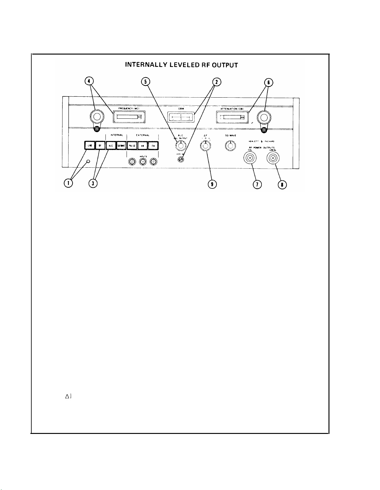
Set FREQUENCY (MHz) low frequency.
Adjust ALC CAL OUTPUT control for desired dBm reference on dBm meter. The ALC system
5.
holds RF output power across the band to within ±1.0 dB for levels of 0 dBm or less. The
most common reference used is —10 dBm because the attenuated RF output power can be read
directly from attenuator readout. Leveled RF output power can be obtained across the band;
however, ATTENUATION (dB) will not accurately calibrate above –10 dBm.
NOTE
Power may be leveled above 0 dBm over that portion of the band where
the desired power is available.
6.
Set ATTENUATION (dB) to desired attenuation. The RF power level at CAL RF POWER
OUTPUT is the algebraic sum of the dBm meter setting and of the ATTENUATION (dB)
setting.
Take leveled and attenuable RF power available at CAL RF POWER OUTPUT.
7.
Take unleveled and unattenuable RF power at UNCAL RF POWER OUTPUT.
8.
9.
Use F control when a small deviation from FREQUENCY (MHz) setting is desired.
3-4
Figure 3-3. Internally-Leveled RF Output
Page 21
TM 11-6625-2820-14&P
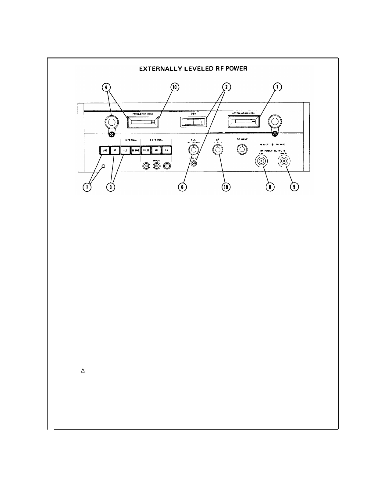
Depress LINE.
1.
Check that meter pointer on dBm meter is on ZERO SET mark.
2.
Depress RF and INTERNAL ALC.
3.
Set FREQUENCY for 1800 MHz.
4.
With a directional coupler connected between CAL output and the load, and as close to the
5.
load as possible, sample and detect incident power and apply the detected signal to INPUT
REMOTE LEVELING phone jack connection (rear panel). Approximately 40 mV but not
more than 240 mV is necessary.
Adjust ALC CAL OUTPUT for desired reference on dBm meter. This reference point may vary
6.
from that used with internal leveling due to different detector sensitivities.
Adjust ATTENUATION (dB) for desired attenuation.
7.
unless a 0 dBm reference has been set while monitoring with a power meter.
Take leveled and attenuable RF power available at CAL RF POWER OUTPUT.
8.
Take unleveled and unattenuable RF power at UNCAL RF POWER OUTPUT.
9.
Use F control when a small deviation horn FREQUENCY (MHz) setting is desired.
10.
The attenuator is not direct reading
Figure 3-4. Externally-Leveled RF Power
3-5
Page 22
TM 11-6625-2820-14&P
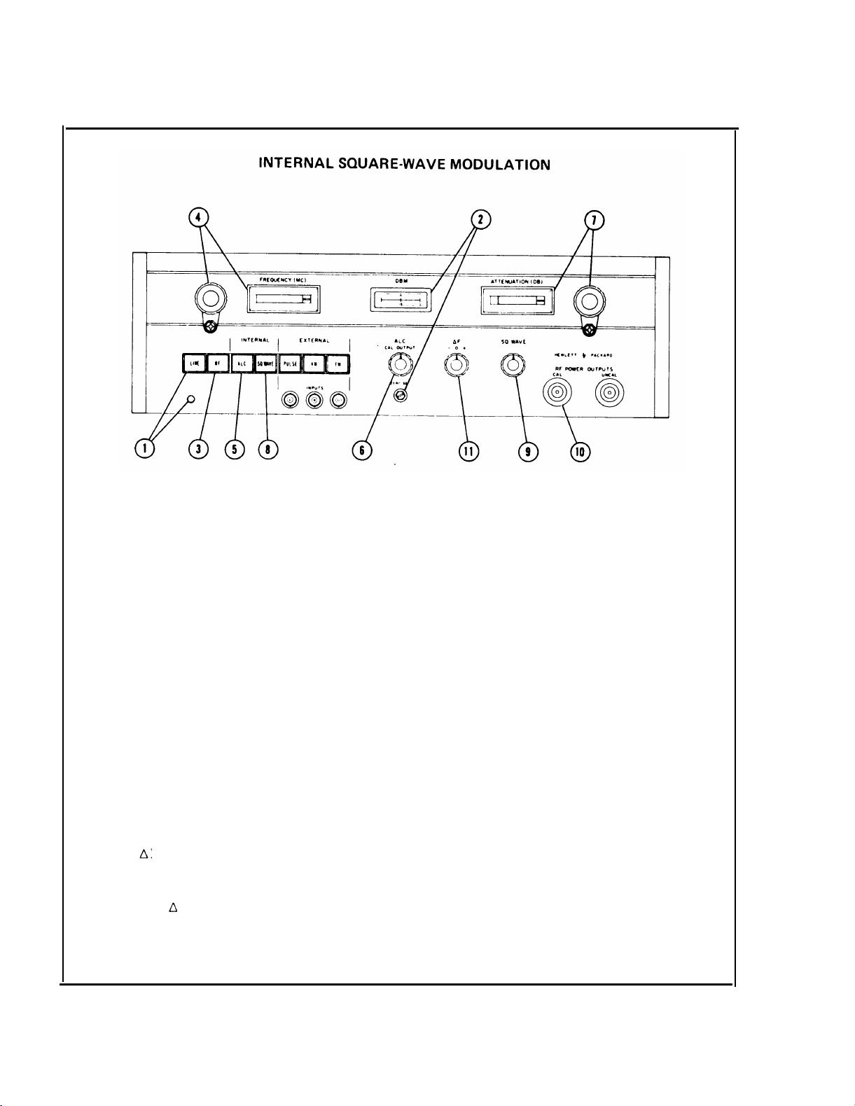
1. Depress LINE.
NOTE
When unleveled power is to be modulated, omit steps 2, 5 and 6.
2. Check that meter pointer on dBm meter is on ZERO SET mark.
3. Depress RF.
4. Set FREQUENCY (MHz).
5. Depress INTERNAL ALC.
6. Adjust ALC CAL OUTPUT for desired dBm reference on dBm meter.
7. Set ATTENUATION dB.
8. Depress SQ. WAVE.
9. Adjust SQ WAVE for desired modulation frequency.
10. Take leveled and attenuable RF power output at CAL RF POWER OUTPUT.
11. Use F control when a small deviation from FREQUENCY MHz setting is desired.
NOTE
F control should be centered when not in use.
3-6
Figure 3-5. Internal Square- Wave Modulation
Page 23
TM 11-6625-2820-14&P
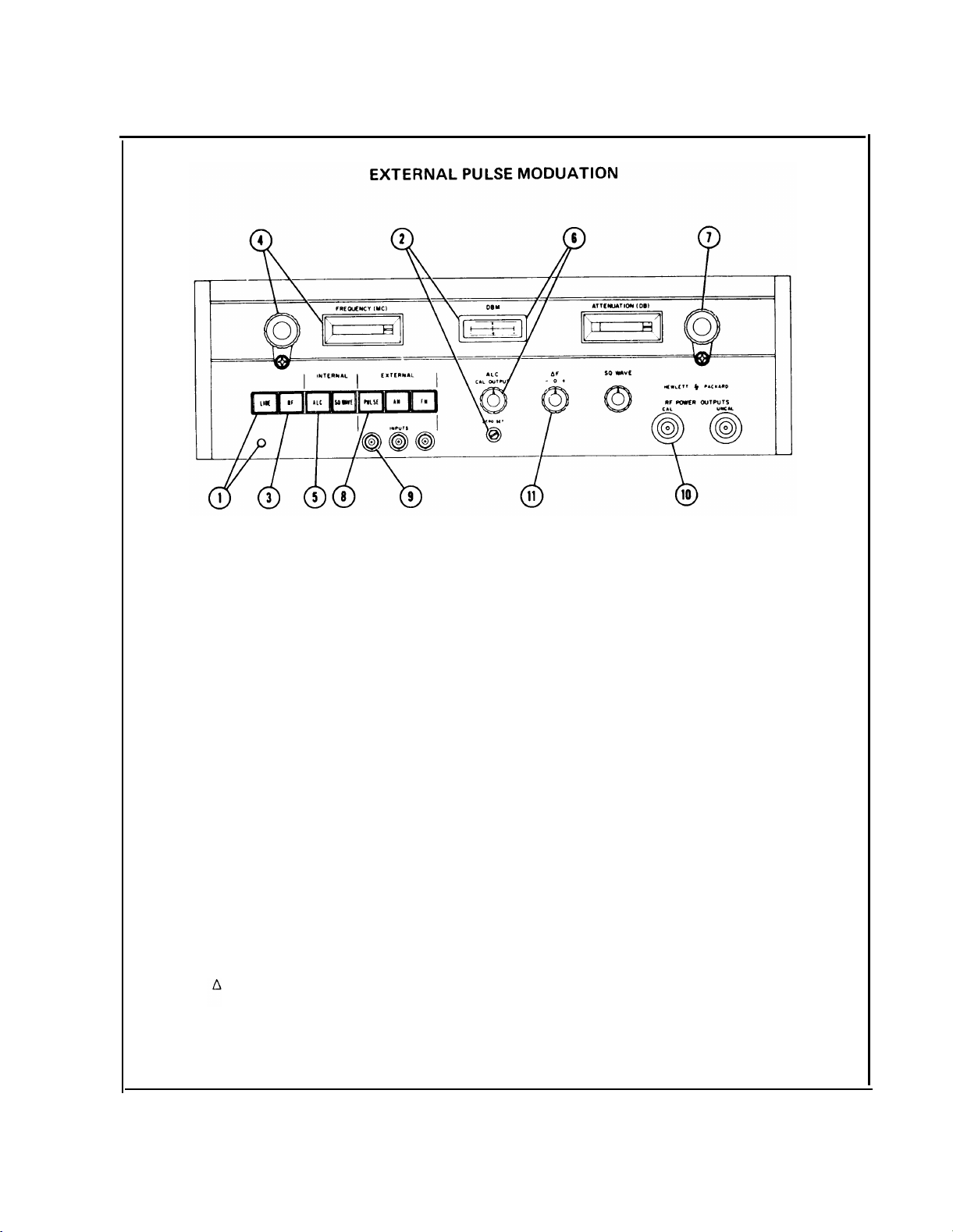
1. Depress LINE.
NOTE
If external pulse modulation of unleveled power is desired, omit steps 2,
5and6.
2. Check that meter pointer on dBm meter is on ZERO SET mark.
3. Depress RF.
4. Set FREQUENCY (MHz).
5. Depress INTERNAL ALC.
6. Adjust ALC CAL OUTPUT for desired dBm reference on dBm meter.
7. Set ATTENUATION (dB) as desired.
8. Depress EXTERNAL PULSE.
9. Apply +20 to +100V 50 Hz to 50 kHz positive pulse modulating signal to EXTERNAL PULSE
INPUT.
10. Take leveled and attenuable pulse modulated RF power output at CAL RF POWER OUTPUT.
11. Use F control when a small deviation from FREQUENCY (MHz) setting is desired.
Figure 3-6. External Pulse Modulation
3-7
Page 24
TM 11-6625-2820-14&P
Depress LINE.
1.
If external FM modulation of unleveled power is desired, omit steps 2, 5, and 6.
NOTE
Check that meter pointer on dBm meter is on ZERO SET mark.
2.
Depress RF.
3.
Set FREQUENCY (MHz).
4.
Depress INTERNAL (ALC).
5.
Adjust ALC CAL OUTPUT for desired dBm reference on dBm meter. The ALC system holds
6.
the RF output power across the band to within limits at frequencies up to 1 kHz provided the
FM voltages are small enough to maintain operation in the center of the mode. The most
common reference used is —10 dBm because the attenuator RF output power can be read
directly from attenuator readout.
NOTE
Power may be leveled above 0 dBm over that portion of the band where the desired power is available.
Set ATTENUATION (dB).
7.
Depress EXTERNAL FM.
8.
Apply modulating signal to EXTERNAL FM INPUT (front or rear panel).
9.
Take leveled and attenuable frequency modulated RF power output at CAL RF POWER
10.
OUTPUT.
Take unleveled FM-modulated RF power at UNCAL RF POWER OUTPUT.
11.
F control should be centered so that the klystron will operate in the center of the mode.
12.
3-8
Figure 3-7. External FM Modulation
Page 25
TM 11-6625-2$20-14&P
1. Depress LINE.
2. Check that meter pointer on dBm meter is on ZERO SET mark.
3. Depress RF.
4. Set FREQUENCY (MHz).
NOTE
If AM modulation of unleveled power is desired, omit steps 5 and 6 and
proceed to step 7. Also, unleveled power can be AM-modulated with a
dc coupled audio signal.
5. Depress INTERNAL ALC.
6. Adjust ALC CAL OUTPUT control for at least 3 dB of attenuation. Due to leveIing at the
frequency desired, the ALC system holds the RF output power across the band to within limits
except for variations due to an AM signal. The most common reference used is —3 dBm because
this allows AM signal to modulate the RF above (3 dB) this level.
7. Set ATTENUATION (dB).
8. Depress EXTERNAL AM.
9. Apply AM modulating signal to EXTERNAL AM INPUT (6 volts peak-to-peak).
10. Take AM-modulated and attenuable RF power output at CAL RF POWER OUTPUT.
11. Use F control when a small deviation from FREQUENCY (MHz) setting is desired.
NOTE
F control should be centered when not in use.
Figure 3-8. External AM Modulation
3-9/3-10
Page 26

Page 27
SECTION IV
PRINCIPLES OF OPERATION
TM 11-6625-2820-14&P
4-1. INTRODUCTION
4-2. Basically the intrument includes a RF
Oscillator, PIN Diode Modulator, Automatic Leveling Circuit, Modulation Circuits, and Power Supply
as shown in Figure 4-1. The RF Oscillator is a
reflex klystron which always operates CW. The PIN
diode modulator is a current-controlled device that
attenuates RF power up to 20 dB or more. The
control circuits provide the modulation currents
required by the PIN modulator. The power supply
provides the regulated dc voltages required to
operate the circuits in the instrument.
4-3. RF OSCILLATOR
4-4. The RF Oscillator, which generates the RF
power, consists of a velocity-modulated tube
operating in an external resonant cavity. The tube
is a reflex klystron operating in the 1-3/4 and 2-3/4
modes.
4-5. The RF power output from the oscillator,
which may be CW or CW with FM, is obtained
from the resonant cavity by means of pickup
probes located in
which open into the resonant cavity. One of these
probes delivers RF power directly to the UNCALIBRATED RF OUTPUT connector, the other two
deliver RF power to the PIN modulator.
small sections of waveguide
4-6. PIN DIODE MODULATOR
4-7. The PIN modulator, which is two nearly
identical units in one, is a high-speed, currentcontrolled absorption-type attenuator. One unit,
the RF attenuator unit, is shown in Figure 4-3. The
second unit, the ALC attenuator unit, is shown in
Figure 4-4. It is a comparison unit. A simplified
illustration of the modulator is shown in Figure
4-2. Each PIN diode unit includes a transmission
line, PIN diodes, low-pass filter, and high-pass
filters.
Figure 4-2. Simplified Block Diagram
of PIN Modulator
Figure 4-1. Circuit Block Diagram
4-8. The PIN diode is a slice of nearly Pure silicon
wafer in which the P and N traces are nearly equal.
P-type impurities are diffused from one side into
the wafer, and N-type impurities are diffused from
the other side, leaving a layer of intrinsic semiconductor (silicon) through the middle. Thus the
name, PIN diode. At frequencies below 100 MHz
the PIN diode rectifies the same as any other good
junction diode. However, at frequencies above 100
MHz, rectification efficiency drops rapidly because
of carrier storage in the intrinsic (I) layer.
4-9. When forward-bias current flows through the
PIN diode, holes and electrons are stored in the I
layer. The more the bias current, the larger the
amount of stored charge-carriers. When reverse bias
is applied, reverse current flows until the stored
carriers are depleted. During this period, the diode
impedance remains 10 w. Currents above several
hundred megacycles do not flow in the reverse
direction for a long enough time to remove those
charge carriers.
So, microwave currents
do not
4-1
Page 28
TM 11-6625-2820-14&P
Figure 4-3. RF Attenuator Unit
significantly change the instantaneous amount of
charge carriers stored, and there is negligible rectification.
4-10. There is, however, a resistance to microwave
current flow. This resistance is inversely
proportional to the number of charge carriers
stored in the I layer, and the number of charge
carriers, in turn, is proportional to the forward bias
current. By varying the bias on a diode from back
bias (no stored charge) to about 1/2 mA forward
bias, the resistance to microwave currents varies
from approximately 5000 ohms to 30 ohms.
4-11. Pin Diodes Mounted in a Transmission
Line.
works, consider a PIN diode mounted across a
transmission line that has a characteristic impedance of 50 ohms. When the diode is back-biased
to about 5000 ohms, the microwave signal on the
transmission line is unattenuated because 5000
ohms compared to 50-ohm line impedance has
little effect. However, when the diode is
To understand how a PIN modulator
4-2
forward-biased to about 30 ohms, most of the
microwave current will flow through the 30-ohm
diode instead of propagating down the 50-ohm
transmission line. This current through the 30-ohm
diode represents microwave energy dissipated as
heat. Consequently the diode actually absorbs
microwave energy.
4-12. Figures 4-3A and 4-4A show the schematic
of the PIN diode modulator used in the Model
8616A. The PIN modulator contains seven PIN
diodes which are placed at approximately 1/4
wavelength along each strip transmission line. The
1/4 wavelength at midband spacing results in the
lowest average SWR because reflection from one
diode will tend to be absorbed and cancelled by
the adjacent diode. The resistance in series with the
diodes reduces voltage to the diodes and thereby
protects the circuit.
4-13. Modulation input in the form of diode bias
is used to change attenuation of the PIN diodes.
Page 29
TM 11-6625-2820-14&P
Figure 4-4. ALC Attenuator Unit
Changes in diode bias produce changes in RF
output level.
4-14. Modulation circuits external to the PIN
modulator are protected by a low-pass filter (Fig-
ures 4-3 and 4-4 ) which prevents RF leakage.
Leakage, if present, could cause erratic action in
the circuits driving the PIN modulator and also
cause RF interference.
4-15. The high-pass filters (Figures 4-3 and 4-4)
permit RF energy to enter and leave the diode strip
line, while keeping the low frequency modulating
signals from entering the RF circuits preceding or
following the PIN modulator.
4-16. MODULATION CIRCUITS
4-17. The arrangement of the modulation circuits
depends on the mode of operation. Mode of
operation switching is accomplished by depressing
the appropriate front-panel button.
4-18. External Pulse
4-19. A simplified diagram of the circuits used in
the external pulse mode of operation is shown in
Figure 4-5. When the pulse button is depressed,
V401A is cut off, and V401B is conducting. The
conduction of V401 B draws current through the
PIN diodes in the REF attenuator unit; hence,
conduction of V401B forward biases the PIN
diodes causing the RF output to decrease by more
than 20 dB. A positive pulse applied to the exter-
nal pulse input turns V401A on, turns V401B off,
and allows RF power to pass through the PIN
diode attenuator with the RF output level clamped
to set level by CR403.
4-20. Internal Square Wave
4-21. A simplified diagram of the circuits used in
the internal square wave mode of operation is
shown in Figure 4-6. When V401B is conducting,
capacitor C402, is
discharging toward
4-3
Page 30
TM 11-6625-2820-14&P
Figure 4-5. Pulse Modulation Circuit
approximately
cut off. When C402 discharges sufficiently, V401 A
begins to conduct and biases V401 B off through
the common cathode resistor R408. This results in
C402 charging toward approximately –225 volts as
long as V401A conducts. When C402 charges
sufficiently however, the current in V401A becomes limited and V401B again conducts causing
V401A to cut off. The RC time constant of C402
is varied by R413, allowing frequency to be
changed from 950 to 1050 Hz. When V401B is
conducting the RF output is cut off by the PIN
diodes. The symmetry of the sqaure wave is ad-
justed by R410. R410 varies the voltage difference
across C402; by varying R410, the time for C402
to charge or discharge to a given potential is
controlled.
4-22. External AM
4-23. A simplified diagram
the external AM mode of
Figure 4-7. With the square
of operation off, V401B is cut off, causing conduction of CR403 which isolates the square wave
and pulse circuit from the AM input and the PIN
diodes. Diode CR403 does this by clamping the
–200 volts while holding V401A
of the circuits used in
operation is shown in
wave and pulse modes
Figure 4-6. Square Wave Modulation Circuit
voltage at the junction of R414 and CR404 at
approximately +0.6 volt. This back biases CR404
providing the isolation.
Figure 4-7. External AM Circuit
4-4
Page 31

TM 11-6625-2820-14&P
4-24. Since the PIN diode modulator is of the
absorption type, it is necessary to lower the average level of the RF carrier (CW power level) by an
amount equal to the peak level of the AM signal so
that the peak will not be clipped. The ALC CAL
adjust sets the power level of the RF carrier. The
external signal then increases or decreases the
attenuation to give amplitude modulation. When
the external signal goes positive, it increases the RF
out of the generator by reducing the current in the
PIN diodes. A negative signal causes an increase in
current in the PIN diodes, which causes a signal
level reduction up to approximately 20 dB on the
negative half cycle of the input depending on
peak-to-peak amplitude of the AM signal. For most
purposes this amount of signal reduction should be
sufficient since it very nearly approximates 10070
modulation. The amount of distortion, though
small, is dependent upon the percentage of modu-
lation: at 30% modulation the amount of distortion is almost unnoticeable; at 100% modulation
the distortion may be as great as 5 to 20%.
4-25. Internal Meter and Automatic Level Control
(ALC)
4-26. A simplified diagram of the ALC circuit is
shown in Figure 4-8. The meter amplifier is a dual
function circuit, performing both a leveling and/or
a power output monitoring function. RF power is
taken from the klystron cavity through the ALC
attenuator assembly (part of the PIN diode modulator) and delivered to the ALC circuit. The meter
amplifier monitors the power level and in leveled
operation with the ALC amplifier, maintains a
constant RF output.
4-27. Actual operation is as follows: RF power
from the klystron is coupled from a fixed probe in
the klystron cavity to the ALC attenuator (part of
the PIN diode modulator). The RF power is deli-
vered through a high-pass filter to the ALC diode
attenuator, then through another high-pass filter to
a crystal detector. The detected signal from CR701
is then delivered to a low-pass filter and to the
ALC circuit.
4-28. The crystal detector CR701 is arranged so
that the detected signal is negative in polarity. An
increase in RF level as the klystron is tuned across
the band will cause a more negative output. A
decrease in RF power from the klystron causes a
less negative output. The detected RF output level
from CR701 is then delivered to the base of
Q501A.
4-29. Consider the circuit operation when the RF
level from the klystron increases. An increase in
klystron output level causes a more negative signal
on the base of Q501A. The conduction of Q501A
decreases causing the collector of Q501A to go in a
positive direction. The positive signal goes through
Figure 4-8. ALC and Meter Circuit
4-5
Page 32

TM 11-6625-2820-14&P
the cathode follower, V401, and is applied to the
base of Q502, decreasing the conduction of Q502.
The collector of Q502 goes more negative.
4-30. A portion of the negative-going signal from
the collector of Q502 is applied to the base of
Q501B as negative feedback. The feedback factor
is determined by the ratio of R513 to R514. The
open loop gain of the meter amplifier (Q501 A/B,
Q502 and Q503) is sufficiently high so that the
closed loop gain is essentially a function of the
feedback factor and is, therefore, less dependent
upon the normal aging effects on the tubes and
transistors in the circuit.
4-31. The negative-going signal from Q502 is also
applied to the meter M501 for output indication.
The meter is protected against overload by the
breakdown diode CR501. If the internal ALC
switch, S601, is on, the negative-going output is
applied to the base of the differential amplifier,
Q601, causing a decrease in conduction. The
collector of Q601 will go more positive, causing an
increase in conduction of the emitter followers,
Q603 and Q604. This causes the emitter of Q604
to also become more positive. The positive-going
signal is applied to the bases of Q605 and Q606
increasing their conduction and causing both collectors to become more negative.
4-35. External Leveling
4-36. A simplified diagram of the ALC circuit is
shown in Figure 4-8. Operation of the external
leveling is the same as that described for internal
leveling with two exceptions. Operation of the
ALC circuit is such that the ALC attenuator (part
of the PIN diode modulator) will no longer be part
of the circuit; therefore, since the ALC attenuator
is removed from the overall circuit, the meter,
M501, will indicate a RF power level but not an
accurate measure of CAL RF OUTPUT power.
4-37. Regulated Power Supply
4-38. There are three regulated power supplies:
high voltage,
supplies are series-regulated types. The series regu-
lator is connected in series with the main load. The
output voltage is monitored and compared to a
reference voltage.
applied through a control amplifier to the series
regulator. This differential voltage changes the
effective resistance of the series regulator which in
turn holds the output voltage constant (see Figure
4-9).
+20 volts, and filament. All three
The voltage differential is
4-32. The collectors of Q605 and Q606 appear as
constant current sources, so the decrease in collector potential causes current to be drawn from the
PIN diodes. This increased bias current (increased
forward bias) reduces the RF power output to its
original level.
Q605 is delivered to the RF PIN diode attenuator
allowing less RF to pass through it also. The net
result is that an increase in klystron output causes
an increase of forward bias on the PIN diodes
which decreases the RF output.
4-33. Leveling Accuracy. For accurate leveling,
the ALC and RF pin diode attenuators must track
together as far as attenuation and frequency are
concerned. The adjustment of R614, R620, and
R621 provide for matching the attenuator charac-
teristics.
4-34. ALC Cal Output. The RF OUTPUT can be
controlled by adjusting the front panel ALC CAL
OUTPUT control which varies the bias on the base
of the differential amplifier, Q602, which in turn
changes the bias on the PIN diode attenuator.
The negative-going output from
Figure 4-9. Series-Regulated Power Supply
4-39. The high-voltage supply consists of two supplies which have been combined to obtain required
voltages. They are a —320 volt supply on which a
–350 volt supply has been stacked to provide a
total of -670 volts. Both supplies use voltage
doublers to drive series regulator circuits. Since this
is a combined circuit arrangement, the —320 volt
and —400 volt supplies are interdependent. There
is also a gas regulator tube, V105, connected to the
– 320 volt supply to provide a –212 volt regulated
source.
4-40. There are two low-voltage supplies. One
provides +20 volts DC for the ALC circuit, the
4-6
Page 33

TM 11-6625-2820-14&P
other 6.1 volts DC for filament operation. The +20
volt supply uses a voltage doubler and series
regulator, while the filament supply uses a halfwave rectifier and a series regulator.
4-7/4-8
Page 34

Page 35

SECTION V
MAINTENANCE
TM 11-6625-2820-14&P
5-1. INTRODUCTION
5-2. This section provides maintenance and service
information for the Model 8616A. Included in this
section is a performance check which may be used
to verify instrument operation (see Appendix II).
5-3. TEST INSTRUMENTS REQUIRED
5-4. Table 5-1 lists test equipment required for the
maintenance procedures discussed in this section.
Instruments other than those recommended may
be used, provided performance meets the basic
requirements given in Table 5-1.
5-5. PERIODIC MAINTENANCE
5-6. Cleaning the Air Filter
5-7. Inspect the air filter regularly and clean it
before it becomes dirty enough to restrict air flow.
Remove filter from instrument rear and
a.
wash it in warm water and detergent.
b. Dry filter thoroughly and
instrument.
5-8. GeneraI Maintenance
5-9. Other than periodic cleaning of
as mentioned above, the Model 8616A requires no
special preventive maintenance. We do suggest,
however, that every six months or so low pressure
air be used to blow any accumulated dust out of
the instrument.
5-10. Cover Removal
5-11. The Model 8616A is equipped with remov-
able top and bottom covers. The top cover exposes
wiring harnesses and the wired side of the powersupply circuit board.
hinged and may be opened out from the instrument when the top cover is removed. When the
power-supply circuit board is opened out from the
instrument, all of the adjustments and tests points
are accessible. The bottom cover exposes resistor
R613 and the wired side of the ALC circuit board.
The power-supply board is
remount on
the air filters
a.
Remove the four flathead screws from
cover.
b. Slide cover back and off instrument.
5-12. TROUBLESHOOTING
5-13. The following troubleshooting procedure
isolates the trouble to a stage. The procedure
should be performed generally in the sequence
given below.
When using an ohmmeter to measure
transistor forward and reverse resistance,
quite a bit of care must be used as almost
every ohmmeter has a few ranges that
supply enough current or voltage to damage a transistor. Before using any ohmmeter, measure the open-circuit voltage
(open-circuit voltage of each range should
not exceed 1.5 volts), and measure the
short-circuit current (current of each
range should not exceed 3 mA). If the
open-circuit voltage and or short-circuit
current exceeds 1.5 volts or 3 mA, respectively ON THE OHMMENTER RANGE
THAT YOU INTEND TO USE then the
ohmmeter will probably damage the transistor to be tested. For example: a DC
Multimeter cannot be used on the Rxl
and Rx10 range, but all other ranges are
perfectly safe.
POWER SUPPLIES. The high-voItage
a.
supply consists of two supplies which have been
combined to obtain the required voltages. They are
a —320 volt supply on which a —400 volt supply
has been stacked to provide a total high voltage
output of —720 volts. Both supplies use voltage
doublers to drive the regulator circuits. There is
also a gas regulator tube connected to the —320
volt supply to provide a —2.1 volt regulated source.
There are two low-voltage supplies. One provides
+20 volts DC for the ALC circuit, the other
provides 6.1 volts DC for filament operation. The
+20 volt supply uses voltage doublers; the 6.1 volt
supply uses half-wave rectifier and transistorized
series regulator circuits.
5-1
Page 36

TM 11-6625-2820-14&P
Table 5-1. Test Equipment Required
5-2
Page 37

TM 11-6625-2820-14&P
(1) LEVEL OUTPUT CHECK
“SOME OF THE MAINTENANCE AND
SERVICING OPERATIONS DESCRIBED
HEREIN ARE PERFORMED WITH
POWER SUPPLIED TO THE INSTRUMENT WHILE COVERS ARE RE-
MOVED.
PERFORMING THESE OPERATIONS.
LINE VOLTAGE IS ALWAYS PRESENT
ON TERMINALS INCLUDING THE
POWER INPUT CONNECTOR, FUSE
HOLDER, POWER SWITCH, ETC. IN
ADDITION, WHEN THE INSTRUMENT
IS ON, ENERGY AVAILABLE AT
MANY POINTS MAY RESULT IN PER-
SONAL INJURY OR DEATH WHEN
CONTACTED.”
Remove four #6 x 32 screws from top
(1)
cover and remove top cover.
Open out power-supply board by re-
(2)
moving two screws that secure board to
leveler assembly.
Connect ac power line to an ac power
(3)
source. Set slide switch at 115 volts ac or
230 volts ac as appropriate.
(4)
Connect a digital voltmeter in parallel and
make the proper measurements (see Table
5-3).
Use grounded meter for filament and
—400 volt measurement.
BE CAREFUL WHEN
(a) Set up Model 8616A as follows:
LINE . . . . . . . . . .
RF . . . . . . . . . . . depressed
ALC not depressed
ATTENUATION “ : : . . . . . 012
FREQUENCY . . . . . 1800 MHz
(b) Using a
measure voltage
Q501A (easiest access is rear
panel REMOTE LEVELING INPUT connector). Specification:
reading should equal 120 ± 2
mV. If voltage is not within
specification refer to paragraph
5-29 and adjust.
(c) With Model 8616A as in step a,
depress ALC button and set dBm
meter with ALC CAL OUTPUT
adjust to 0 dBm. Using dc millivolt meter measure voltage on
base of Q501A. Specification:
voltage should be approximately
100 mV.
(d) Set up power meter combination
for operation on the 3 mW range.
(e) Using power meter measure the
CAL RF OUTPUT of the Model
8616A across the entire fre-
quency range. Specification:
Level output should be constant
within ± 1.0 dB.
dc millivolt meter
depressed
on base of
b. TROUBLESHOOTING LOCATION
CHART. Check instrument trouble symptoms
against those listed in Table 5-2, Trouble Location.
ISOLATING TROUBLE TO A SPECIFIC
c.
CIRCUIT. Because each mode of operation uses
different circuit combinations (see Figure 5-1),
trouble can be isolated to a specific circuit by
checking the operation of each mode of operation
in logical order.
ISOLATING TROUBLE TO THE PIN
d.
MODULATOR. This procedure isolates trouble to
the PIN diode modulator box or to the instrument
circuitry.
(f) If level output is not within
specification refer to paragraph
5-28 and check and if necessary
adjust klystron repeller voltages
across frequency band.
(g) AIso, refer to paragraph 5-33 and
check and if necessary adjust the
ALC Amplifier for proper opera-
tion.
(h) Recheck signal generator leveled
output. If level output is still not
within
Table 5-2 eliminate cause of
specification refer to
5-3
Page 38

TM 11-6625-2820-14&P
5-4
Figure 5-1. Model 8616A Block Diagram
Page 39

Table 5-2. Trouble Location
TM 11-6625-2820-14&P
Table 5-3. Power Supply Adjust
5-5
Page 40

TM 11-6625-2820-14&P
trouble to either the PIN diode
modulator box or instrument circuitry.
(2) ON-OFF RATIO CHECK. Refer to
paragraph 5-42.
5-14. REPAIR
5-15. The etched circuit boards used in the 8616A
are of the plated-through type and consist of a base
board and conductor. The board does not include
funneled eyelets. The conductor material is plated
to the wall of the holes and thus the conductor is
effectively extended through the hole. This type of
board can be soldered from either the conductor or
component side of the board with equally good
results. The rules given below should be followed
when repairing a plated-through type etched circuit
board .
Avoid applying excessive heat when sol-
dering on the circuit board.
b. To remove a damaged component, clip
component leads near the component, then apply
heat, and remove the leads with a straight upward
motion.
outer truarc ring from the outer cover of the
klystron cavity (see Figure 5-2).
d. Remove outer cover. Remove inner truarc
ring holding klystron clamp housing in klystron
cavity.
Pull tube socket from klystron with a
e.
straight pull. Grasp klystron tube and remove from
cavity.
f.
Unscrew clamp nut, lift out clamp spacer,
and remove klystron (see Figure 5-2).
Remove waffle washer from cavity.
g
NOTE
Refer to paragraph 1-13
rant y claim instructions.
5-18. Tube Replacement
a. Reassemble new klystron, housing, spacer,
and nut.
b. Set klystron frequency drive at top end
(high frequency dial setting) for klystron centering.
for klystron war-
c. Use a special soldering iron tip to remove
components having multiple connections, such as
potentiometers, transformers, etc. Refer to Table
5-1 for type of soldering tip required.
d. Use a toothpick to free hole of solder
before installing a new component.
5-16. KLYSTRON REMOVAL AND REPLACE–
MENT
5-17. Tube Removal
BEFORE ATTEMPTING KLYSTRON
REMOVAL OR REPLACEMENT, BE
CERTAIN THAT LINE POWER IS COMPLETELY REMOVED FROM INSTRUMENT.
a. Remove panel cover on left (with
respect to front panel) side of instrument
(see Figure 5-2).
Set klystron frequency drive at top end
(4500 MHz frequency dial setting).
c. Using truarc pliers which are available in a
repair kit, HP Part No. 08614-800, remove the
Place waffle washer in klystron cavity.
c.
d. Insert klystron into klystron cavity.
Klystron should be inserted straight into
cavity. Insertion of klystron should require no unnecessary force; the klystron
should fit snugly but easily, into cavity.
Replace inner truarc ring on clamp hous-
e.
ing (if the klystron is properly in place the ring will
fit properly). Allow tube to be centered by center
conductor.
Install tube socket and outer cover.
f.
Place edge of truarc ring on outer cover
g.
and rotate until ring lies flat on cover and is easily
accessible with truarc pliers.
Refer to Calibration Checks (paragraph
h.
5-26) and make necessary adjustments.
5-19. RF PROBE REMOVAL AND REPLACE-
MENT
5-20. Probe Assembly Removal
5-6
Page 41

TM 11-6625-2820-14&P
Figure 5-2. Cut-A way View of Klystron Cavity and Klystron Assembly
BEFORE
ASSEMBLY REMOVAL OR REPLACEMENT,
POWER IS COMPLETELY REMOVED
FROM INSTRUMENT.
Remove top cover from instrument.
a.
b. Set FREQUENCY (MHz) drive to the
highest frequency setting (4500 MHz).
c.
Remove Attenuator access cover from
Klystron Cavity Casting and disconnect
assembly connectors from instrument.
d. Remove the cable assembly connector
from the defective RF probe cable. Be careful not
to lose any connector parts as they will be required
for reassembly.
Remove
e.
guide.
ATTEMPTING
BE CERTAIN THAT LINE
the probe cable from the cable
PROBE
cable
Remove the retaining screw holding the
f.
tuning carriage and remove the probe from the
casting.
The defective probe assembly should be
g.
returned to your local Hewlett-Packard Sales and
Service Office for repair or replacement (see list at
rear of manual).
5-21. Probe Replacement
THE
SHOULD BE HANDLED WITH CARE.
THE PROBLE SHOULD BE PLACED IN
A PROTECTIVE SHIELD WHEN HANDLING OR SHIPPING.
a.
insert the new probe into the Klystron Cavity
Casting and replace the probe retaining screw.
PROBE IS
To install a new probe assembly, carefully
FRAGILE AND
5-7
Page 42

TM
11-6625-2820-14&P
CARE MUST BE TAKEN NOT TO
DAMAGE THE RESISTIVE ELEMENT
ON THE PROBE END OR THE SPRING
WIPERS THAT MAKE CONTACT WITH
THE PROBE GUIDE TUBE.
f.
Trim the dielectric flush with the end of
the clamping body so that the center conductor is
bare.
Trim the center conductor protruding
g.
from the clamping body, then place the insulator
washer on the center conductor.
b. Insert the probe assembly through the
cable guide. Install the cable guide.
c.
Trim the insulation from the end of the
problem assembly cable (for RF UNCAL probe, 5/16
inch; for RF CAL and ALC probes, 1/4 inch).
d. Place cable assembly connector parts on
cable, with the exception of the clamping body,
and fold the braid upon the connector assembly
(see Figure 5-3).
Place the clamping body on the RF UN-
e.
CAL cable and screw the clamp nut and clamping
body together.
NOTE
After tinning center conductor the diameter may be too large to fit into the pin,
making it necessary to file the center
conductor to the proper diameter.
h. In preparing the ALC and CAL RF
probes, cut the inner conductor insulation about
1/8” from folded braid.
i.
Flatten inner conductor to approximately
1/8” wide and 1/32” thick.
Tin flattened conductor with solder and
j.
allow it to wick slightly.
5-8
Figure 5-3. RF Probe Assembly
Page 43

TM 11-6625-2820-14&P
k. Press end of inner conductor with
ensure good contact and smooth insertion
Cal.
Before connecting connector assembly in-
1.
to the instrument, connect an ohmmeter between
the probe center
measure the resistance across the range of the
attenuator. The resistance should be approximately
50 ohms ±5 ohms. If the probe is open or shorted
at any point, the probe is defective and should be
replaced.
m. Replace the connector assembly as it was
before disassembly. Connect the probe connector
to the instrument, making certain the center conductor makes good contact.
The probe installation is complete. Reas-
n.
sembly the instrument except for the front, right
side panel, which is removed when performing the
output power calibration adjustments.
5-22. PIN MODULATOR REMOVAL AND RE-
PLACEMENT
5-23. Modulator Removal
5-24. The PIN modulator CANNOT be repaired in
the field. If the PIN modulator is found to be
faulty, it should be returned for repair. Remove
the four screws holding the PIN modulator only.
Removal of screws holding the PIN diodes in place
can cause contamination of the PIN diodes, high
SWR, etc.
a. Remove power line from instrument.
b.
Remove top and bottom covers.
conductor and ground and
a file to
recepti-
f. (Referring to Figure 5-14 and paragraph
5-54) replace crystal diode body.
Disconnect ALC Bias Feed connections (1
g.
and 2 on A500 board) from ALC circuit board.
h. Remove three screws holding PIN modula-
tor in place.
i.
Remove PIN modulator from instrument.
Carefully pack PIN modulator in a con-
tainer and return to your local Hewlett-Packard
field office for repair or replacement.
5-25. Modulator Replacement
Replace three screws that hold PIN mod-
a.
ulator to instrument chassis.
b. Connect RF OUTPUT cable to J701.
Connect ALC Bias Feed connections to
ALC circuit board (A500).
d. Connect cable assembly connectors to
PIN diode modulator. (See CAUTION, paragraph
5-24).
e.
Place crystal diode into modulator; the
dark-coated side of crystal fits into the finger of
center conductor. WHEN INSTALLING CRY-
STAL, DO NOT FORCE TIP OF CRYSTAL INTO
CENTER CONDUCTOR AS FINGERS IN
MOUNT MAY BE DAMAGED OR BENT. Bending
or damaging center conductor fingers will cause
sporadic operation of the diode.
c. Place instrument on its side.
DO NOT HANDLE CRYSTAL DIODE,
CR701 NEEDLESSLY. A static charge
which builds up on a person, especially on
a cold, dry day must NEVER, be allowed
to discharge through element. When installing always touch casting first to insure
no difference in potential between hand
and casting.
d. (Referring to Figure 5-19 and paragraph
5-54) disconnect crystal diode, CR701, and crystal
diode body, P706, from PIN modulator.
e.
Disconnect cable assembly connectors
from the modulator (see Figure 5-3). Be careful
not to lose any disassembled parts as they will be
required for reassembly.
f. (Referring to Figure 5-14 and paragraph
5-54) replace crystal diode body.
5-26. CALIBRATION
5-27. Regulated Power-Supply Adjustment
Remove instrument top cover and open
out top circuit board (see paragraph 5-10).
b. Depress LINE button.
c.
Connect ac power line to an ac power
source. Set ac voltage at 115 or 230 volts as
appropriate.
d. Connect DC voltmeter digital and vacuum
tube voltmeter in parallel and make necessary
adjustments (see Table 5-3).
5-9
Page 44

TM 11-6625-2820-14&P
Use ungrounded meter for filament and
--400V measurement.
Figure 5-4. PIN Modulator (External View)
5-28. Frequency Tracking, Preliminary
tors; a fuse holder, and a power cord. Connected as
shown, this modulator provides a power line frequency modulation voltage continuously variable in
amplitude from 300 volts peak-to-peak, with phase
variable over a range of approximately 80 degrees,
plus a 6.3-volt AC output for oscilloscope sweep
control.
d. Apply external FM (60 cycles) and view
mode patterns on oscilloscope. Adjust PHASE
control of FM modulator and adjust tracking pot
(R219) for mode pattern shown in Figure 5-5.
e.
With Frequency Tracking adjustment
completed, measure klystron beam current: Using
a clip-on milliammeter, connected to wire on center feedthrough capacitor (C4), current must not
exceed 30 mA.
5-29.
Power Adjustment
a. Connect dc digital voltmeter between the
klystron repeller white/purple/yellow wire coming
from center conductor support rod past relay
switch between PIN DIODE BOX and Klystron
Cavity Casting and ground. Make sure F control
on front panel is set at zero (center of pot range),
and proceed as indicated in Table 5-4.
Table 5-4. Klystron Repeller Voltages
b. At a dial frequency of 1800 MHz set
ATTENUATOR dial for a calibrated output of
about 0 dBm.
c. To observe repeller modes of the klystron,
a FM Modulator, with adjustable phase and amplitude controls, is necessary. Such a device is shown
in Figure 5-5; it consists of a small power transformer connected with the primary and secondary
windings interchanged; two one-megohm potentiometers; a 0.01 µF capacitor; two BNC connec-
5-30. RF Power Output Adjustment.
Front Panel Settings: Have ALC button
released (OFF). Set ATTENUATION (dB) to 0.12
dB. Set FREQUENCY to 1800 MHz.
b. CAL RF Adjustment:
(1)
With a power meter, measure the
CAL RF output power. It should be
–11 dBm ±0.1 dBm.
If it is not, loosen the two set screws
(2)
in the attenuator drive shaft bevel
gear with your fingers until the output power is –11 dBm. Without disturbing the –11 dBm power setting,
turn the attenuator knob on the front
panel until the attenuator counter
reads 012 dB. Tighten the two set
screws in the bevel gear.
c. UNCAL RF Adjustment:
(1) Measure the UNCAL RF power out-
put. It should be –3 dBm ±0.3 dBm.
(2) If it does not, the RF UNCAL probe
requires adjustment. The front, right
panel should be removed, exposing
the probe assembly cable guide.
Remove the screw in the cable guide
that is in line with the UNCAL probe
retaining screw (see Figure 5-11).
Insert a long Allen wrench through
the hole left by removing the cable
guide screw into the UNCAL probe
retaining screw.
screw to adjust the UNCAL probe
Turn the retaining
5-10
Page 45

TM 11-6625-2820-14&P
Figure 5-5. Frequency Tracking Setup
5-11
Page 46

TM 11-6625-2820-14&P
penetration for –3 dBm ±0.3 dBm
output.
d. ALC Adjustment:
(1) With a dc voltmeter (HP Model
412A) measure the dc voltage at the
output of the CR701 crystal diode, or
the base of Q501A.
DO NOT USE A DIGITAL VOLTMETER
WITH AUTO-RANGING AS IT MIGHT
DAMAGE THE CRYSTAL DIODE.
(2)
The dc voltage should be 120 mV ±2
mV.
(3)
If it is not, the ALC attenuator probe
requires adjustment. The front, right
side panel should be removed, exposing the probe assembly cable guide.
Remove the screw in the cable guide
that is in line with the ALC probe
retaining screw (see Figure 5-13). Insert a long Allen wrench through the
hole left by removing the cable guide
screw into the ALC probe retaining
screw. Turn the retaining screw to
adjust the ALC probe penetration for
120 mV ±2 mV at the ALC crystal
output .
5-32. Frequency Tracking
a.
Use a frequency
actual frequency at ‘dial settings of 1800 and 4500
MHz. To eliminate backlash error, always approach
frequency settings in the same direction.
b. The difference in frequency meter readings for Model 8616A dial settings should be 2700
MHz.
c. Refer to graph, Figure 5-6. The horizontal
axis represents the measured frequency change
from step b, the vertical axis indicates the dial
corrective setting. For example, if the difference
between dial settings (step b) is 2177 MHz, the
corrective setting for the dial as found on the graph
is 1805 MHz. To make the corrective setting, set
the frequency dial to 1800 MHz, loosen the two
setscrews that clamp the dial plunger to the rack,
shift the dial to 1805 MHz, and then tighten the
two setscrews.
d. If any plunger adjustment was necessary
(step c), repeat Frequency Tracking, Preliminary
Adjustments (paragraph 5-28). Repeat this pro-
cedure until rotation from low to high frequency
corresponds to a change of 2700 MHz ±6 MHz.
e.
Set actual frequency to 1800 MHz.
Loosen spur gear on counter shaft and rotate gear
until frequency dial reads approximately 1801.5
MHz.
Final
meter to measure the
5-31. Meter Amplifier
Turn off RF power. Zero front panel
meter with front panel ZERO SET.
b. Depress RF button and measure meter
amplifier output voltage (junction of R515 and
C502). This voltage must be -6.4 ±0.3V at 1800
MHz. This corresponds to a gain of 53 ±2.
Front panel meter should read ±1.2 ±0.2
dBm.
Table 5-5. Klystron Probe Adjust
5-12
f.
Check FREQUENCY (MHz) dial settings
at both upper and lower ends of dial travel. The
respective dial end points should be less than 1800
MHz and greater than 4500 MHz. If dial travel is
not satisfactory then loosen bevel gear on frequency drive shaft and reset dial.
Check microswitch action: The micro-
g.
switch
(2988
switch
switch
should
should energize and de-energize at about
to 3012 MHz). If microswitch does not
at the proper dial settings then the microcam (located on underside of cavity casting)
be repositioned.
Page 47

Figure 5-6. Frequency Trucking
h. Being careful to approach all dial settings
from the same (either clockwise or counterclock-
wise) direction, using the procedure given in para-
graph 5-38, check the accuracy of the frequency
dial by approaching all dial settings from a clock-
wise direction and then from a
direction.
NOTE
The Frequency Meter used
brated to an accuracy of approximately
counterclockwise
must be cali-
(±0.07%).
If frequency dial reading errors are greater
i.
than ±10 MHz then shifting the dial may bring all
errors within specification. If shifting dial will not
sufficiently correct errors then it may be necessary
to shift the position of center conductor support
rod (see Figure 5-11). The center is held in place
by a notched captive screw at the end closest to
the right side of the instrument which must be
loosen to allow center conductor adjustment “in”
“out”
or
center conductor rod so that original position may
always be known.
positive, adjust center conductor toward right side
of instrument. When adjusting center conductor
position never
thousandths of an inch at a time.
of the klystron cavity. Notch or scratch
If overall frequency dial was
change by more than about 20
TM 11-6625-2820-14&P
If any adjustment of instrument was nec-
j.
essary
procedure until no adjustment is required.
5-33. ALC Amplifier
and ATTENUATION (dB) Of 012.
dBm meter to 0 dBm by means of ALC CAL
OUTPUT knob.
PUT and adjust as indicated in Table 5-6;
power meter and a thermistor mount.
repeat
Set FREQUENCY (MHz) to 1800 MHz
Depress ALC button and set front panel
b.
Track ALC amplifier at CAL RF OUT-
entire
Table 5-6. ALC Amplifier Adjust
check and adjustment
use a
NOTE
A dial reading of 1800.5 MHz when the
actual frequency was 1800 MHz is a positive error.
5-13
Page 48

TM 11-6625-2820-14&P
5-34. Pulse Modulation Adjust
a.
externally-generated 20V, 3 µsec positive pulse to
the front panel pulse BNC input.
sufficient to completely pulse modulate the CAL
RF output power. This condition is achieved when
the ON side of the detected pulse begins to exhibit
a flatness.
5-35. Square-Wave Adjust
detected square wave output from CAL RF OUTPUT on an oscilloscope.
±50 Hz,
5-35A. AM Adjust
graph 5-45).
change value of C404 by approximately 10 pF and
recheck operation.
Depress PULSE button and apply an
b. Adjust R404 so that the input pulse is just
a.
Depress SQ WAVE button and display
b. Adjust R410 for best symmetry at 1000
NOTE
The value of C402 may be 2250 pF, 2676
pF, or 3000 pF depending upon which
value will give the instrument square wave
frequent y range needed.
a.
Check AM operation at 50 Hz (see para-
b. If AM waveform is not satisfactory,
NOTE
5-36. PERFORMANCE CHECKS
5-37. The performance check procedures are used
to check the instrument against its specifications.
All checks are made from the front panel, thus the
instrument panels need not be removed. The procedure is useful in incoming or outgoing quality
control check, periodic maintenance, or afterrepair check.
paragraphs 5-38 and 5-46.
5-38. Frequency Range and Accuracy
a.
5-7.
b. Set up Model 8616A as follows:
LINE . . . . . . . . . . . . . . . . . . . . . . . .
RF . . . . . . . . . . . . . . . . . . . . . . . . . .
c.
an 1800 MHz dial indication on the Model 8616A.
d. Set frequency meter to approximately
1800 MHz and note actual signal frequency.
e.
to a frequency dial indication of 4500 MHz.
be 1800 to 4500 MHz, accuracy of dial indication
should be ±10 MHz.
Repeat above procedure every 100 MHz
f.
Frequency range of Model 8616A should
Performance checks are given in
Connect instrument as shown in Figure
depressed
depressed
Set power meter for a mid-scale reading at
Typically, undistorted AM operation is
achieved with either a 30 or a 39-pF
capacitor.
Figure 5-7. Frequency and Power Measurement
5-14
5-39. F Control Check
a. Connect instrument as shown in Figure 5-7.
Page 49

TM 11-6625-2820-14&P
b. Setup Model 8616A as follows:
LINE . . . . . . . . . . . . . . . . . . . . depressed
RF . . . . . . . . . . . . . . . . . . . . . . depressed
FREQUENCY . . .
Set power meter for amid-scale reading.
c.
d. Turn F control fully counterclockwise
and measure output frequency with power meter
and frequency meter.
e. Turn F control fully clockwise and
measure output frequency.
f. The difference between the readings, steps
d and e, should be approximately 1.5 MHz.
5-40. Power Output Check
a. Connect instruments as shown in Figure
5-7, omitting the frequency meter.
b. Set up Model 8616A as follows:
LINE . . . . . . . . . . . . . . . . . .
RF . . . . . . . . . . . . . . . . . . . .
FREQUENCY . . .
ALA . . . . . . . . . . . . . . . . .
Power output at UNCAL RF OUTPUT
c.
should be at least 0.5 mW.
d. Maximum power output at CAL RF OUT-
PUT should be at least 2 mW.
5-41. Leveled Output Check
a. Connect instruments as shown in Figure
5-7, omitting the frequency meter.
Set up Model 8616A as follows:
b.
frequencies of interest
. . depressed
. . depressed
frequencies of interest
not depressed
d. Noting power meter variation from setting
(step c), tune Model 8616A across frequency band.
The variation should not exceed ± 1.0 dB.
5-42.
Pin Diode On-Off Ratio
a. Connect instruments as shown in Figure
5-7, omitting the frequency meter.
b. Set up Model 8616A as follows:
LINE . . . . . . . . . . . . . . . . . .
RF . . . . . . . . . . . . . . . . . . . . . .
FREQUENCY . . . . . . . . . mid-frequency
EXTERNAL PULSE . . . .
ATTENUATION . . . . . . . . . . . ..+9 dB
ALA . . . . . . . . . . . . . . . . .
c. Set power meter on +10 dBm scale and
adjust Model 8616A ATTENUATION control for
convenient reference.
d. Depress EXTERNAL PULSE on Model
8616A.
e. Reference on the power meter should
change to the
off ratio must be at least 20 dB.
f. If the on-off ratio is not 20 dB or greater,
the PIN modulator may be defective. Check bias
current through R414 and R420: the current
through R414 should be approximately 6 mA, and
the current through R420 should be 3 mA. If these
bias currents are correct, the modulator is defective
(refer to paragraph 5-22) or CR403 shorted.
543. Internal Square-Wave Check
a.
5-8.
–10 dBm scale. Specification: On-
Connect instruments as shown in Figure
. . depressed
depressed
not depressed
not depressed
LINE . . . . . . . . . . . . . . . . . .
RF . . . . . . . . . . . . . . . . . . . .
FREQUENCY . . . . . . . . . . ..1800 MHz
ALA . . . . . . . . . . . . . . . . . . . .
ALC CAL OUTPUT . . . counterclockwise
NOTE
Before ALC button is depressed, dBm
meter should indicate approximately +1
dBm; depressing ALC button should cause
d13m meter indication to decrease. ALC
CAL OUTPUT: 0 dBm (dBm meter indication); ATTENUATOR (dB): --0 dB or
less.
c. Set power meter for convenient mid-scale
reading.
. . depressed
. . depressed
. depressed
b. Set up Model 8616A as follows:
LINE . . . . . . . . . . . . . . . . . . . .
RF . . . . . . . . . . . . . . . . . . . . . .
INTERNAL SQ WAVE . . . . . . depressed
ATTENUATION . . . . . . . . . . . . . .0 dB
SQ WAVE . . . . .
c.
Set oscilloscope sweep time to .1
MHz/cm.
d. Readjust rate control to display one complete square wave on oscilloscope. Square wave
symmetry should be better than 45/55%. Range
should be 950 to 1050 Hz.
fully counterclockwise
depressed
depressed
5-15
Page 50

TM 11-6625-2820-14&P
Figure 5-8. Internal Square Wave Check
5-16
Figure 5-9. External Pulse Check
Page 51

TM 11-6625-2820-14&P
544. External Pulse Check
Connect instruments as shown in Figure
a.
5-9.
b. Setup Model 8616A as follows:
LINE . . . . . . . . . . . . . . . . . . . .
RF......................
EXTERNAL PULSE . . . . . .
Set up pulse generator for a 20-volt 50 prf
c.
depressed
depressed
depressed
signal with a pulse width of 3 µsec.
d. A pulse presentation should be seen on
the oscilloscope. Specification rise time: 2 µsec max.
e.
Set up pulse generator for a 20-volt
5000-prf signal with a pulse width of 3 µsec.
A pulse presentation should be seen on
f.
the oscilloscope. Specification rise time: 2
µsecmax.
545. External AM Check
Connect instruments as shown in Figure
5-10.
b. Setup Model 8616A as follows:
LINE . . . . . . . . . . . . . . . . . . . .
RF......................
EXTERNAL AM . . . . . . . . . . .
ALC. . . . . . . . . . . . . . . . ....
depressed
depressed
depressed
depressed
ALC CAL OUTPUT –3 dBm (dBm meter)
FREQUENCY . . . . . . . . . . ..1800 MHz
ATTENUATION . . . . . . . . . 0 dB or less
Apply a 6 *0.1 volt peak-to-peak l-kHz
c.
sine wave to front panel BNC input.
d. Using ALC CAL OUTPUT to vary DC
level of detected sinusoid, center wave so there is
no peak clippings (vary input amplitude, if neces-
sary).
Figure 5-10. External AM Check
Change 2
5-17
Page 52

TM 11-6625-2820-14&P
e.
Adjust vertical sensitivity of the oscilloscope to give
detected 1 kHz signal
a 6-cm vertical display of the
and then increase signal
frequency to 1 MHz. The vertical display of the 1
MHz signal should be greater than 3.0 cm.
546. MEASUREMENT OF RESIDUAL AND IN-
CIDENTAL FM
a. Connect instruments as shown in Figure
5-12, without the test oscillator in the setup.
b. Setup Model 8616A as follows:
d. Roll of masking tape (1/2-inch or 1-inch,
width).
e.
Rubber cement.
549.
Procedure
5-50. If it is necessary to replace the cam cable,
order it by HP Stock No. 08614-299 and descrip
tion
of usage. For easier access to the cams, remove
the screws holding the High Voltage circuit board
and swing the board out of the way. Use Figures
5-11 and 5-13 as a guide and proceed as follows:
LINE . . . . . . . . . . . . . . . . . .
RF . . . . . . . . . . . . . . . . . . . .
. . depressed
. . depressed
FREQUENCY . . . . . . . . . . . . . 2.5GHz
c.
Adjust frequency meter output for 10
kHz/V. Line sync oscilloscope.
d. Adjust transfer oscillator for 125 MHz
and Harmonic of 200.
e.
Adjust frequency for 10 kHz difference
frequency reading on frequency meter.
f. Residual FM (line related components)
reading (“peak to trough”) on oscilloscope is less
than 250 mV peak (250 mV = 2500 Hz).
Set up Model 8616A as follows:
g.
INTERNAL SQ WAVE . . . . . . depressed
ATTENUATION . . . . . . . . . . . .–10dB
h. Incidental FM is negligible.
i.
Connect instruments as shown in Figure
5-12, with the test oscillator in the setup.
Set up Model 8616A as follows:
j.
a.
Remove power cord from instrument.
b. Remove instrument top cover and atten-
uator access cover.
c.
Turn FREQUENCY (MHz) to approxi-
mately the middle
d. Orient Length Cam to Frequency Cam as
of the frequency band.
shown in Figure 5-11.
e.
Using a lead pencil, mark the position of
each cam and the end of the threaded portion of
the center conductor support rod on the klystron
cavity casing.
f.
Using the hex socket wrench and a 3/8inch open-end wrench, remove both terminal
screws,
the four washers, and the two nuts
(10-32x0.375; hex nuts).
Remove both terminal screws horn cable.
g.
h. On replacement cable, place a mark half-
way between each end. Using matches apply heat
to an area approximately 1/2 to 3/4-inch on either
side of the mark to remove wire tension (heat to
nearly white hotness.
EXTERNAL FM . . . . . . . . . .
. depressed
i.
Cut 10 or 11 strips of masking tape,
approximate y 1-inch in length.
k. Adjust test oscillator for a 10 kHz, 5 to 6
volt peak modulating signal.
j.
Remove 3 retaining screws from Frequency Cam and remove cam from instrument
1.
Incidental FM is negligible.
5-47. CAM CABLE REPLACEMENT k. Slide cable through one terminal screw so
(Note: 3 retaining screws are 4-40x0.625, FH).
that cable is secured to terminal screw as shown in
5-48. Tools Required
Figure 5-13, for the Frequency Cam, and install
terminal screws on Frequency Cam.
a.
Open-end wrench (3/8-inch).
b. Hex-socket wrench and 3/8-inch socket or
equivalent tool.
Be careful not to catch cable between
c.
Book of matches.
5-18
lockwasher and cam.
PIN : 032939-002
Page 53

TM 11-6625-2820-14&P
Figure 5-11. Top View, Cover Removed
5-19
Page 54

TM 11-6625-2820-14&P
Figure 5-12. Residual and Incidental FMCheck
Figure 5-13. Exploded View – Cam Assembly
Page 55

TM 11-6625-2820-14&P
m. Slide cable onto cam just past point A and
B; the other half should pass over points C, D, and
E).
NOTE
Each cam as shown in Figure 5-13 has two
lips along which the cable should travel,
one cable must travel along the upper lip,
of both cams and one cable must travel
along the lower lip of both cams.
n.
Slide other half portion of cable onto cam
just past point D and tape to cam.
Place Frequency Cam in original position
o.
in instrument and replace retaining screws.
Turn Length Cam so that cams are not
p.
touching at point F and place cable between cams:
on cable along upper lip of cam and the other
along lower lip of lip of cam.
Turn Length Cam so that it is apparently
q.
touching Frequency Cam at point F and place two
pieces of masking tape across the two cams at
point F.
step e, the other marks made should match
appropriately.
w. Perform Frequency Tracking adjustments,
paragraph
5-28 and 5-32.
5-51. LOW PASS FILTER REPLACEMENT
5-52. Took Required
Low heat soldering iron and solder (flux)
a.
b. Small pair needle nose pliers.
c.
Small pair pliers.
5-53. Procedure
5-54. Figure 5-14 illustrates Low Pass Filter and
ALC crystal diode (CR701) parts with stock numbers. The illustration is an assembly drawing. Part
removal is the reverse of illustrated assembly in-
structions. The first step for disassembly is to
unsolder the cable to low pass filter and grounding
lug connections. The last step of assembly is to
solder the cable to Low Pass Filter and grounding
lug connections.
r.
With the cams held together, slide the
cable which passes over points C and D past point
E and the cable which passes over point A past
point B and tape each portion of cable to the cam.
NOTE
It is important that each cable portion
have as little slack between it and the
cams as possible: a loose cable causes
backlash.
s.
Slide cable ends through second terminal
screw so that cable is secured to terminal screws as
shown in Figure 5-13, for the Length Cam.
t. Install the second terminal screw on the
Length Cam and tighten both terminal screws to
remove all slack in cable.
u.
Remove masking tape from cams and
apply rubber cement to ends of cable to ensure
that cable will not unravel.
v. Turn FREQUENCY (MHz) knob to
match Frequency Cam to pencil mark made in step
Before touching CR701 refer to paragraph
5-24, step c – Caution.
5-55. CAVITY WIPER REPLACEMENT
5-56. The following procedure will enable you to
easily replace the wipers in the cavity of the 8616A
signal generators. These wipers may need to be
replaced when holes appear in the FM mode
pattern and the klystron is known to be good.
5-57. Parts Required
5-58. The correct parts to order are listed below:
HP Part Number
08616-210
08614-282
5-59. Replacement Procedure
1.
Set the attenuator to –20 dBm. This will
Description
Wiper, Cavity
Conductor, Center
prevent damage during the wiper replacement,
Quantity
2
1
5-21
Page 56

TM 11-6625-2820-14&P
5-22
Figure 5-14. Low Pass Filter Assernbly Drawing
Page 57

TM 11-6625-2820-14&P
2. Remove
bottom, and trim
3. Place instrument on left side frame and
unsolder repeller filter lead from bottom of main
deck (white, yellow, violet). There are two leads
the same color, so be sure to remove lead going to
the cavity.
4.
Remove two lower cavity retaining screws
that hold cavity halves together, and remove the
UNCAL RF probe.
5. Place instrument on right side frame;
remove klystron cover plate on left side of instrument, then remove klystron.
6. Place instrument on its bottom and remove all screws and covers from right side frame
and remove the right side frame.
7. Slide off base casting plate from ends of
cavity probe guide and center conductor support
rods.
8. Remove attenuator casting cover from top
of cavity casting.
all instrument
strips.
covers, top and
shafts to the right. Place right cavity half so that
wipers are facing upward. Right cavity half and
tuning carriage may offer some resistance during
removal. A small plastic hammer may be used to
free the two cavity halves from each other.
15. Be very careful to prevent damaging
probes and remove the three screws from center
ring of wipers that hold the wipers to the tuning
carriage.
16. Using a thin bladed screwdriver between
back of outer wiper and teflon bearing plate,
remove outer wiper.
damage probes. Remove teflon bearing plate and
three metal spacers. Note the placement of the
wipers.
17. Now remove inner wiper from the support
rods and clean any excess silver paint from probe
guide tubes.
18. Inspect new wipers for bent fingers. Carefully slide a new wiper over probe guide tubes. It
may require tapping with plastic hammer around
the wiper back plate to make wiper slide into
position.
Again be careful not to
9. Use a sharp scribe or awl and mark tuning
carriage position on its tuning rod. Also mark
position of center conductor rod at right side of
casting. Then loosen shaft clamp on center conductor.
10. Tune frequency control to high frequency
stop. Use long nose pliers to grip center conductor
and slide to left out of the cavity. A new
center conductor should also be installed when
wipers are changed. Tune to the low frequency
stop and remove the frequency tuning and attenuator knobs.
11. On left side of instrument remove the
four screws holding cavity casting and three screws
into front panel under forward trim strip.
12. Carefully slide front panel and cavity
assembly to right until left mainframe side is
disengaged from front panel. Now slide front panel
forward until tuning and attenuation shafts are
clear. Tilt panel forward as far as possible without
breaking any leads.
13. Loosen two screws in top of tuning carriage that hold carriage to its tuning shaft. Now
remove two screws from cavity top that hold
cavity halves together.
14, Using your right hand, gently slide the
right cavity half and tuning carriage off tuning
19. Place toothpicks in screw holes of support
rods. Slide metal spacers over toothpicks followed
by teflon bearing and outer wiper. Again, outer
wiper may require gentle tapping to seat fully into
position.
NOTE
Holes are not symmetrical in teflon bearing or wipers.
20. Holding the cavity upright remove one
toothpick at a time and install the wiper retaining
screws. Be careful spacer does not move when a
toothpick is removed.
21. Although not necessary, the use of a small
amount of silver paint around probe guide tubes
and the three wiper retaining screws is recom-
mended. This will help prevent RF leakage.
22. Using paper tissues, remove any excess
lubricant from inside of cavity. Use a small amount
of Moly coat on another tissue and clean inside of
cavity so that cavity walls feel lubricated, but no
grease can be seen.
23. Again, holding left cavity half in left hand
and right cavity half in right hand, slide the right
half over the tuning shafts being careful to line up
tuning carriage holes.
5-23
Page 58

TM 11-6625-2820-14&P
Be very careful not to damage wiper
fingers during assembly.
24. Slide the two halves together until the
tuning carriage can be pushed far enough forward
for wipers to enter cavity. Now slowly push tuning
carriage to the left until the wipers enter the bevel
at the edge of the left cavity half. Now carefully
slide wiper into cavity body until both wipers are
fully inside cavity.
repeller filter. Insert allen wrench into the
center conductor, alongside repeller filter
lead, and use only enough pressure to
slowly slide repeller filter out of the center conductor.
30. Slide tuning carriage back to mark pre-
viously scribed on tuning shaft during disassembly,
and tighten two screws in top of tuning carriage.
31. Now follow steps 12 through 1 disas-
sembly in reverse to re-assemble the instrument.
25. Carefully slide cavity halves together and
re-install the two upper allen retaining screws into
cavity assembly.
26. Now take new center conductor and
scribe mark on shaft in approximately the same
location as previously done on the old center
conductor.
27. Use silver polish and clean outer surface
of center conductor to remove all oxidation. Using
same procedure as on cavity walls, lightly wipe on
and wipe off Moly coat lubricant.
28. Now roll center conductor along clean
bench or table to form the fingers until they are a
firm fit over klystron grid ring. (See Figure 5-15.)
32. The instrument will need to have both the
power output and frequency re-calibrated after this
procedure (refer to paragraphs 5-28 through 5-32).
5-60. Frequency Drive Gear Replacement
5-61. The frequency drive gear HP Part Number
08614-245, has been changed to an all brass gear.
The following procedure will speed up replac-
ing the gear:
1. Tune the generator to mid-band. Use a
scribe to draw a line across the tops of the two
frequency cams marking where they touch.
2. Wrap about four inches of masking tape
around the ends of each cam to hold down the
stainless steel anti-backlash wires.
3. Remove the three 4-40x.625 inch screws
holding each cam. Very carefully lift off the cams
as a unit.
cams fold over, the stainless steel wires will have to
be restrung and the job will take about three times
as long. Place cams under something heavy enough
to hold them flat while you finish replacing gear.
Do not allow the cams to fold over. If
Figure 5-15. Forming the Center
Conductor Fingers
29. Remove the repeller filter from the old
center conductor and re-install the repeller filter in
new center conductor. Now lay center conductor
assembly aside temporarily y.
NOTE
It will be necessary to use a long, ten inch
or longer, allen wrench to remove the
5-24
4. Mark on casting, position of one of screw
holes on gear.
5. Turn signal generator upside-down. Re-
move bottom cover.
6. Remove the two 6-32x3/8 inch screws
holding 2.625 inch repeller pot cover.
7. Mark on edge of casting location of rotor
contact.
8. Loosen the two number 6 hex head set
screws holding rotor. Remove rotor.
9. Write down location and color code of 4
wires connected to repeller potentiometer. Note
location of terminal lugs and connections on inside
of repeller potentiometer.
Page 59

TM 11-6625-2820-14&P
10. Remove the four 4-40xl/2 inch screws
holding connection to repeller potentiometer.
11. Mark position of the contact lug on P.C.
board mounted under potentiometer resistor.
12. Loosen nylon screw holding contact lug.
Lift out wire wound resistor, insulator and P.C. Refer to paragraph 5-38 to check freboard.
13. Use 1/2 inch drive socket wrench and
remove nut holding gear shaft. Remove gear.
14. Install new gear. Reverse disassembly pro-
cedure and mount all necessary parts.
NOTE
quency range and accuracy.
5-25/5-26
Page 60

Page 61

Page 62

Page 63

Page 64

Page 65

Page 66

Page 67

Page 68

Page 69

SECTION VI
REPLACEABLE PARTS
TM 11-6625-2820-14&P
6-1. INTRODUCTION
6-2. This section contains information for ordering
parts. Table 6-l lists abbreviations used in the parts
list and throughout the manual. Table 6-2 lists all
replaceable parts in reference designator order.
Table 6-3 contains the names and addresses that
correspond to the manufacturer’s code number.
6-3. ABBREVIATIONS
6-4. Table 6-1 gives a list of abbreviations used in
the parts list, schematics, and throughout the
manual. In some cases, two forms of the abbreviation are given,
partial or no capitals.
abbreviations in the parts list are always all capitals. However, in the schematics and other parts of
the manual, other abbreviation forms are used with
both lower case and upper case letters.
6-5. REPLACEABLE PARTS LIST
6-6. Table 6-2 is the list of replaceable parts and is
organized as follows:
Electrical assemblies and their compo-
a.
nents in alpha-numeric order by reference designation.
b.
Chassis-mounted parts in alpha-numeric
order by reference designator.
Miscellaneous parts.
c.
one all capital letters and one
This occurs because the
d. Illustrated parts breakdown.
The information given for each part consists of
the following:
a.
The Hewlett-Packard part number.
b. The total quantity (Qty) in the instru-
ment.
c.
The description of the part.
d. Typical manufacturer of the part in a
five digit code.
e.
Manufacturer code number for the part.
The total quantity for each part is given only
once; at the first appearance of the part number in
the list.
6-7. ORDERING INSTRUCTIONS
6-8. To order a part listed in the replaceable parts
table, quote the Hewlett-Packard part number,
indicate quantity required, and address the order
to the nearest Hewlett-Packard office.
6-9. To order a part that is not listed in the
replaceable parts table, include the instrument
model number, instrument serial number, the description and function of the part, and the number
of parts required. Address the order to the nearest
Hewlett-Packard office.
6-10. Refer to table 6-4 for part
number to NSN cross-reference.
6-1
Page 70

TM 11-6625-2820-14&P
Table 6-1. Reference Designations and Abbreviations (1 of 2)
6-2
Page 71

Table 6-1. Reference Designations and Abbreviations (2 of 2)
TM 11-6625-2820-14&P
6-3
Page 72

TM 11-6625-2820-14&P
Table 6-2. Replaceable Parts
6-4
Page 73

Table 6-2. Replaceable Parts
TM 11-6625-2820-14&P
6-5
Page 74

TM 11-6625-2820-14&P
Table 6-2. Replaceable Parts
6-6
Page 75

Table 6-2. Replaceable Parts
TM 11-6625-2820-14&P
6-7
Page 76

TM 11-6625-2820-14&P
Table 6-2. Replaceable Parts
6-8
Page 77

Table 6-2. Replaceable Parts
TM 11-6625-2820-14&P
6-9
Page 78

Page 79

TM 11-6625-2820-14&P
PART NUMBER - NATIONAL STOCK NUMBER
TABLE 6-4 (Contd.)
CROSS REFERENCE INDEX
DRSEL-MA Form 6230, (1 Sep 76)
6-11
HISA-FM 1909-
Page 80

TM 11-6625-2820-14&P
PART NUMBER - NATIONAL STOCK NUMBER
Table 6-4 (Cont'd.)
CROSS REFERENCE INDEX
6-12
DRSEL-MA Form 6230, (l Sep 76)
HISA-FM 1909-
Page 81

APPENDIX O
REFERENCES
TM 11-6625-2820-J4&P
Appendix O
DA Pam 310-4
DA Pam 310-7
TM 38-750
TM
750-244-2
Index of Technical Manuals, Technical Bulletins,
Supply Manuals (Types 7, 8, and 9), SupplY
Bulletins,
US Army
Orders.
The Army Maintenance Management System (TAMMS).
Procedures for Destruction of Electronics
Materiel to Prevent Enemy Use (Electronics
Equipment Index of Modification Work
Command).
and Lubrication Orders.
0-1
Page 82

Page 83

APPENDIX I
MANUAL CHANGES
TM 11-6625-2820-14&P
I-1. INTRODUCTION
I-2. This section
adapting this manual to instruments for which the
content does not apply directly. Refer to Table A-1
Manual Changes by Serial Number. Table A-2
relates individual component changes on assemblies
to the MANUAL CHANGES. In addition,
information about recommended modifications for
improvements to the instruments is provided in
Table A-3.
contains information for
I-3. MANUAL CHANGES
I-4. To adapt this manual to your instrument,
refer to Table A-1 and make all of the manual
changes listed opposite your instrument serial
number. Perform these changes in the sequence
listed.
I-5. If your instrument serial number is not listed
on the title page of this manual or in Table A-1
below,
MANUAL CHANGES supplement.
it may be documented in a yellow
i-1
Page 84

TM 11-6625-2820-14&P
Table A-l. Manual Changes by Serial Number
Table A-2. Manual Changes by Assembly
i-2
Page 85

I-6. MANUAL CHANGE
CHANGE A
Table 6-2:
Change:
R614 and R615 to HP Part No. 2100-0409
R620 and R621 to HP Part No. 2100-0410.
CHANGE B
Figure 5-16 and Table 6-2:
Delete
R700
Figure 5-20:
Change the Component Location Diagram to the one shown in Figure 7-1.
CHANGE C
Table 6-2:
Change:
C401 to 0150-0052, C:FXD CER 0.05 µF 20% 400 VDCW, 56289, 33C17A
R402 to 0687-3931, R:FXD COMP 39K ohm 10% 1/2 W, 01121, EB 3931
R403 to 0687-4741, R:FXD COMP 470K ohm 10% 1/2 W, 01121, EB 4741
Figure 5-16.
Change the value of:
C401 to 0.05
R402
R403
to
39K
to 470K.
TM 11-6625-2t320-l4&P
CHANGE D
Table 6-2:
Add :
08614-608, CABLE ASSY: RF INPUT
08614-609, CABLE ASSY : RF OUTPUT
08614-610, FILTER: LOW PASS.
NOTE
If any of the above components in Change D fail, they must be replaced by the
components listed in paragraph 5-51. In addition, a procedure for disassembly
and assembly of the component parts is included in paragraph 5-51.
Table 6-2:
Delete:
08614-622
08614-623.
Figure 5-18:
Change the diagram with the partial schematic shown in Figure 7-2.
CHANGE E
Figure 5-19 and Table 6-2:
Delete F2
Figure 5-21 and Table 6-2:
Delete CR203.
i-3
Page 86

TM 11-6625-2820-l4+&P
i-4
Figure A-l. High Voltage Board (A1OO)
Page 87

TM 11-6625-2820-14&P
Table 6-2:
Delete under reference designation F2:
1400-0008, Fuseholder
CHANGE F
Table 6-2:
Change F2 to 2110-0029, FUSE: CARTRIDGE 3 AMP 125V SLOW BLOW, 75915, 313005
Figure 5-19:
Change the value of F2 to 4A
CHANGE G
Figure 5-16 and Table 6-2:
Delete R6
CHANGE H
Figure 5-16:
Change R700 to 0687-1031, R:FXD COMP 10K ohm 10% 1/2 W, 01121, EB 1031
Figure 5-19:
Change Cl to 0180-0128, C:FXD ELEC 2800 µF +50-10% 30 VDCW, 56289, D35718 DFP
Table 6-2:
Change the value of:
Cl to 2800
R700 to 10K
CHANGE I
Paragraph 2-10:
Change the fourth sentence to:
A 1-1/2 ampere standard fuse is used for 115 volt operation;
230 volt operation.
Table 6-2:
Change F1 to:
2110-0043, FUSE: CARTRIDGE 1.5 AMP 250V (115V operation), 75915, 31201.5
2110-0033, FUSE: 0.75 AMP 250V (230V operation), 75915, F02GR750A
Change:
J2 to 1251-0148
S2
to
3101-0033
W1 to 8120-0078
Figure
5-19:
Change F1 description:
PAtol.5A
1A to 0.75A
CHANGE J
Table 6-2:
Change:
R6 to 0757-0059, R:FXD MET FLM 1 MEGOHM 1% 1/2 W, 28480,0757-0059
Figure 5-16:
Change the value of R6 to lM
a 3/4 ampere standard fuse is used for
i-5
Page 88

TM 11-6625-2820-14&P
CHANGE K
Table 6-2:
Change:
DSI to 1450-0048, INDICATOR: GLOW LAMP
NEON-RED LENS, 08717, 859-R-5
CHANGE L
Table 6-2:
Change the HP Part Number and Manufacturer Part Number of:
S1 to 3101-0042
S3 to 3101-1153
S401, S402, S403 and S601 to 3101-0043
08616-00005 to 08616-001
CHANGE M
Table 6-2:
Change:
R620 and R621 to 2100-0898, R:VAR WW 500 ohm 5% LIN 1 W, 28480, 2100-0898
CHANGE N
Table 6-2:
Delete:
5000-8709
5000-8711
5060-8713
5060-8736
5060-8740
08616-00007
08616-00008
i-6
Figure A-2. Partial Schematic of Figure 5-17 ALC Circuit (Part of Change D)
Page 89

Table A-3. 8616A Recommended Changes
TM 11-6625-2820-l.4&P
i-7/i-8
Page 90

Page 91

APPENDIX II
ILLUSTRATED PARTS IDENTIFICATION
SIGNAL GENERATOR
TM 11-6625-2820-14&P
8616A
ii-1
Page 92

11-2
REF.
1
2
STOCK NO,
DESCRIPTION
See
Figure B-2
See
Figures B-3 & B-4
REF.
STOCK NO DESCRIPTION
QTY.
REF.
STOCK NO.
DESCRIPTION
QTY.
3
4
5
6
Figure B-5
See
Figure B-6
See
See
Figure B-7
Figure B-8
See
Page 93

ii-3
Figure B-1. HP Model 8616A, Signal Generator, General Arrangement
Page 94

ii-3
Page 95

ii-5
Figure B-2.
HP Model 8616A, Signal Generator, Control Panel
Page 96

Page 97

Page 98

Page 99

Page 100

 Loading...