

Page 1

Errata
Title & Document Type: 8562E Spectrum Analyzer Service Manual
Manual Part Number: 08562-90216
Revision Date: 1997-12-01
HP References in this Manual
This manual may contain references to HP or Hewlett-Packard. Please note that HewlettPackard's former test and measurement, semiconductor products and chemical analysis
businesses are now part of Agilent Technologies. We have made no changes to this
manual copy. The HP XXXX referred to in this document is now the Agilent XXXX.
For example, model number HP8648A is now model number Agilent 8648A.
About this Manual
We’ve added this manual to the Agilent website in an effort to help you support your
product. This manual provides the best information we could find. It may be incomplete
or contain dated information, and the scan quality may not be idea l. If we find a better
copy in the future, we will add it to the Agilent website.
Support for Your Product
Agilent no longer sells or supports this product. You will find any other available
product information on the Agilent Test & Measurement website:
www.tm.agilent.com
Search for the model number of this product, and the resulting product page will guide
you to any available information. Our service centers may be able to perform calibration
if no repair parts are needed, but no other support from Agilent is available.
Page 2

Service Guide
HP 8562E Spectrum Analyzer
HEWLETT
Fia
HP Part No. 08582-90218 Supersedes 08582-90209
Printed in USA December 1997
PACKARD
Page 3

Notice.
The information contained in this document is subject to change without notice.
Hewlett-Packard makes no warranty of any kind with regard to this material, including
but not limited to, the implied warranties of merchantability and fitness for a particular
purpose. Hewlett-Packard shall not be liable for errors contained herein or for incidental or
consequential damages in connection with the furnishing, performance, or use of this material.
@
Copyright Hewlett-Packard Company 1996
All Rights Reserved. Reproduction, adaptation, or translation without prior written
permission is prohibited, except as allowed under the copyright laws.
1400 Fountaingrove Parkway, Santa Rosa, CA 95403, USA
Page 4
Certification
Hewlett-Packard Company certifies that this product met its published specifications at the
time of shipment from the factory. Hewlett-Packard further certifies that its calibration
measurements are traceable to the United States National Institute of Standards and
Technology, to the extent allowed by the Institute’s calibration facility, and to the calibration
facilities of other International Standards Organization members.
Regulatory Information
The HP 8560 E-Series Spectrum Analyzer Calibration Guide contains regulatory information.
Warranty
This Hewlett-Packard instrument product is warranted against defects in material and
workmanship for a period of one year from date of shipment. During the warranty period,
Hewlett-Packard Company will, at its option, either repair or replace products which prove to
be defective.
For warranty service or repair, this product must be returned to a service facility designated
by Hewlett-Packard. Buyer shall prepay shipping charges to Hewlett-Packard and
Hewlett-Packard shall pay shipping charges to return the product to Buyer. However, Buyer
shall pay all shipping charges, duties, and taxes for products returned to Hewlett-Packard
from another country.
Hewlett-Packard warrants that its software and firmware designated by Hewlett-Packard for
use with an instrument will execute its programming instructions when properly installed on
that instrument. Hewlett-Packard does not warrant that the operation of the instrument, or
software, or firmware will be uninterrupted or error-free.
LIMITATION OF WARRANTY
The foregoing warranty shall not apply to defects resulting from improper or inadequate
maintenance by Buyer, Buyer-supplied software or interfacing, unauthorized modification or
misuse, operation outside of the environmental specifications for the product, or improper
site preparation or maintenance.
.
NO OTHER WARRANTY IS EXPRESSED OR IMPLIED. HEWLETT-PACKARD
SPECIFICALLY DISCLAIMS THE IMPLIED WARRANTIES OF MERCHANTABILITY
AND FITNESS FOR A PARTICULAR PURPOSE.
EXCLUSIVE REMEDIES
THE REMEDIES PROVIDED HEREIN ARE BUYER’S SOLE AND EXCLUSIVE
REMEDIES. HEWLETT-PACKARD SHALL NOT BE LIABLE FOR ANY DIRECT,
INDIRECT, SPECIAL, INCIDENTAL, OR CONSEQUENTIAL DAMAGES, WHETHER
BASED ON CONTRACT, TORT, OR ANY OTHER LEGAL THEORY.
. .
III
.
Page 5
Assistance
Product maintenance agreements and other customer assistance agreements are available for
Hewlett-Packard products. For any assistance, contact your nearest Hewlett-Packard Sales and
Service
Ofice.
Safety Notes
The following safety notes are used throughout this manual. Familiarize yourself with each of
the notes and its meaning before operating this instrument.
Caution
Warning
Instruction
Manual
Caution denotes a hazard. It calls attention to a procedure that, if not
correctly performed or adhered to, could result in damage to or destruction
of the instrument. Do not proceed beyond a caution sign until the indicated
conditions are fully understood and met.
Warning
correctly performed or adhered to, could result in injury or loss of life. Do
not proceed beyond a
understood and met.
The instruction manual symbol. The product is marked with this symbol when it is
necessary for the user to refer to the instructions in the manual.
denotes a hazard. It calls attention to a procedure which, if not
warning
note until the indicated conditions are fully
iv
Page 6
General Safety Considerations
Warning
Warning
Caution
This is a Safety Class I product (provided with a protective earthing ground
incorporated in the power cord). The mains plug shall only be inserted in a
socket outlet provided with a protective earth contact. Any interruption of the
protective conductor, inside or outside the instrument, is likely to make the
instrument dangerous. Intentional interruption is prohibited.
No operator serviceable parts inside. Refer servicing to qualified personnel. To
prevent electrical shock, do not remove covers.
Before switching on this instrument, make sure that the line voltage selector
switch is set to the voltage of the power supply and the correct fuse is
installed.
V
Page 7
How to Use This Guide
Chapter 7, “General Troubleshooting,”
can be used to identify the location of a problem to a
board or functional area in the spectrum analyzer.
Chapters 8 through 13, which cover the functional areas, can then be used to help you localize
the problem further.
Once the faulty area is identified, the adjustments and parts information located in chapters 1
through 6 is available to help you fix the problem.
This guide uses the following conventions:
Front-panel
Sof
Screen Text
tkq
Key)
This represents a key physically located on the instrument.
This indicates a “softkey,”
a key whose label is determined by the instrument
firmware.
This indicates text displayed on the spectrum analyzer screen.
Documentation Outline
HP 8560 E-Series Spectrum Analyzer Calibration Guide
n Tells you how to run verification software.
n Tells you the specifications of your spectrum analyzer.
n Tells you how to test your spectrum analyzer.
HP 8560
n Tells you how to make measurements with your spectrum analyzer.
n Tells you how to install the spectrum analyzer.
n Tells you how to program your spectrum analyzer.
HP 8560 E-Series Spectrum Analyzer Quick Reference Guide
n Is an abbreviated version of the HP 8560 E-Series Spectrum Analyzer User’s Guide.
n Provides you with a listing of all remote programming commands.
HP 8560 E-Series Spectrum Analyzer Component Level Information
n Provides schematics and parts lists for the instrument.
E-Series
Spectrum
Analyzer
User’s Guide
vi
Page 8

Contents
1. General Information
Serial Numbers and Repair Information
Instrument Variations
HP 85629B Test and Adjustment Module
Service Kit
Electrostatic Discharge
Reducing Potential for ESD Damage
Static-Safe Accessories
Returning Instruments for Service
Service Tag
Original Packaging
0 t her Packaging
Recommended Test Equipment
Sales and Service Offices
2. Adjustment Procedures
.Introduction
Safety Considerations
Which Adjustments Should Be Performed?
Test Equipment
Adjustable and Factory-Selected Components
Adjustment Tools
Instrument Service Position
Using the TAM
Test Equipment
Adjustment Indicator
Front End Cal (adjustment)
1. High Voltage Power Supply Adjustment
2. Display Adjustment
3. IF
4. IF Amplitude Adjustments
5. DC Log Amplifier Adjustments
6. Sampling Oscillator Adjustment
7. YTO Adjustment
8. LO Distribution Amplifier Adjustment
9. Frequency Response Adjustment
10. Calibrator Amplitude Adjustment
11. 10 MHz Reference Adjustment-OCXO (Non-Option 103)
12. 10 MHz Reference Adjustment-TCXO (Option 103)
13. Demodulator Adjustment
14. External Mixer Bias Adjustment (Non-Option 327)
15. External Mixer Amplitude Adjustment (Non-Option 327)
..............................
.............................
Bandpass
.................
.........................
................
........................
.................
........................
....................
............................
.........................
..........................
.....................
........................
........................
...............
...........................
..............
..........................
.....................
............................
...........................
........................
......................
...............
.......................
Adjustment
........................
.....................
....................
..................
..................
...............
..................
.................
......
........
.....................
.........
......
l-l
l-2
l-3
l-4
l-4
l-5
l-6
l-6
l-6
l-6
l-7
l-9
1-16
2-l
2-2
2-2
2-2
2-2
2-3
2-3
2-9
2-9
2-9
2-12
2-13
2-15
2-21
2-26
2-30
2-34
2-37
2-40
2-43
2-47
2-48
2-51
2-53
2-56
2-57
Contents-l
Page 9

16. YIG-Tuned Filter/Mixer (RYTHM) Adjustment
17. 16 MHz PLL Adjustment
18. 600 MHz Reference Adjustment
3.
Frequency Response Adjustment Software
Getting Started
Spectrum Analyzers
Controller (Computer)
Test Equipment
Warmup Time
............................
.........................
........................
...........................
...........................
Test Equipment Warmup
Spectrum Analyzer Warmup
Equipment Connections
Computer (Controller) Setup
.....................
..................
.....................
....................
.......................
....................
HP-IB Cables ..........................
10 MHz Reference .........................
Adjustment Setups ........................
Using Frequency Response Adjustment Software
Loading the Program
Program Operation
Conditions Menu
Test Record Header Information
System Mass Storage File Location
........................
.........................
..........................
..................
.................
Power Sensors ..........................
Setting HP-IB Addresses
......................
Storing and Loading the Conditions File
Getting to the Adjust Menu
....................
Verifying the HP-IB ........................
Querying the Spectrum Analyzer Serial Number
Exiting Frequency Response Adjustment
Dual-Bus Operation ........................
Sensor Utilities Menu
Adding a Power Sensor Data File
........................
..................
Viewing and Editing a Power Sensor Data File
Deleting a File
..........................
Changing the System Mass Storage File Location
Listing Available Power Sensor Data Files
Returning to the Conditions Menu
Adjust Menu
............................
.................
Single Test ............................
Calibrate Power Sensor
......................
List Equipment ..........................
Frequency Response Adjustment Menu Softkeys
Conditions Menu
Sensor Utilities Menu
Adjust Menu
..........................
........................
............................
Front End Cal (YIG-Tuned Filter/Mixer (RYTHM) and Frequency
Response Adjustment)
.....................
Frequency Response Adjustment Error Messages
Error Messages Beginning with Alphabetic Characters
Address must be from 0 to 30 inclusive
...........
.............
...............
...........
...............
............
...........
..............
.............
.............
..........
...............
2-60
2-63
2-66
3-2
3-2
3-2
3-3
3-3
3-3
3-3
3-4
3-4
3-4
3-4
3-4
3-5
3-5
3-5
3-6
3-6
3-6
3-6
3-7
3-7
3-8
3-8
3-8
3-8
3-8
3-9
3-9
3-10
3-10
3-10
3-10
3-10
3-10
3-11
3-11
3-11
3-12
3-12
3-12
3-13
3-14
3-16
3-16
3-16
Contents-2
Page 10
Cal Factor outside of 0 to 150% range entered
............
CONDITIONS file from system file location is not compatible! WARNING
Conditions Menu DUT ID disagrees with responding DUT ID .....
Data not accepted, check entry format ................
DUT doesn’t respond at address listed ................
File <filename> not found .....................
Insufficient equip. to do test <test number> : <test name> ......
No HP-IB address listed for DUT ..................
Non-numeric entry other than S entered, or frequency
<=O
......
No sensor file found for <sensor model> S/N <sensor serial #> ....
Power meter reads <value>
Select code
<value>
does not currently support HP-IB operations
dBm
..................
...
Sensor serial number must be from 1 to 99999 ............
System mass storage file location catalog cannot be read ........
This program does not support the current DUT ...........
Unable to load CONDITIONS file from listed system file location
....
Unable to load data from <sensor filename> .............
Unable to obtain catalog from <system mass storage file location>
Unable to reach power level of <value>
dBm
.............
...
WARNING: CONDITIONS file from system file location is not compatible!
Error Messages Beginning with Numeric Characters ...........
8481A Sensor cal data minimum frequency not <= 50 MHz ......
8481A Sensor cal data maximum frequency not >= 300 MHz ......
8485A Sensor cal data minimum frequency not = 10 MHz .......
8485A Sensor cal data maximum frequency not >= 26.5 GHz .....
Error Messages Beginning with Variables ...............
<filename> file not found .....................
<keyboard entry> is a non-numeric entry ..............
<number of instruments> instruments have HP-IB addresses of <HP-IB
address> ...........................
<power meter model number> doesn’t read signal to be in -1 +/-5
range
<source model number> signal not in +5 +/-5
<source model number> signal not in -1 +/-5
<source model number>
.............................
dBm
range ......
dBm
range ......
+lO dBm
signal not in
+lO
+/-8
dBm
range
dBm
.
<source model number> has a cold oven ...............
<source model number> is unlevelled ................
3-16
3-16
3-16
3-16
3-16
3-17
3-17
3-17
3-17
3-17
3-17
3-17
3-17
3-17
3-17
3-18
3-18
3-18
3-18
3-18
3-18
3-18
3-18
3-18
3-18
3-19
3-19
3-19
3-19
3-19
3-19
3-19
3-19
3-19
3-19
4. Assembly Replacement
Access to Internal Assemblies ......................
Cable Color Code ...........................
Procedure 1. Spectrum Analyzer Cover ................
Procedure 2. Al Front Frame/Al8 CRT ...............
Procedure 3.
Procedure 4.
Procedure 5. A2, A3, A4, and A5 Assemblies
Procedure 6. A6 Power Supply Assembly
Procedure 7.
AlAl
Keyboard/Front Panel Keys ............
AlA
RPG
......................
.............
...............
A6Al
High Voltage Assembly ..............
Procedure 8. A7 through Al3 Assemblies ...............
A7 First LO Distribution Amplifier
A8 Low Band Mixer
.........................
..................
4-2
4-3
4-4
4-5
4-13
4-14
4-15
4-21
4-25
4-28
4-30
4-31
Contents-3
Page 11

A9 Input Attenuator
A10 YIG-Tuned Filter/Mixer (RYTHM)
AllYTO
.............................
Al3 Second Converter
Procedure 9. Al4 and Al5 Assemblies
........................
................
........................
................
Procedure 10. Al6 Fast ADC and Al7 CRT Driver ...........
Procedure 11. Bl Fan
Procedure 12.
BTl
Procedure 13. Rear Frame/Rear Dress Panel
Procedure 14. W3 Line Switch Cable
Procedure 15. EEROM (A2U500)
Procedure 16. A21 OCXO
.......................
Battery
.....................
.............
.................
..................
......................
5. Replaceable Parts
Ordering Information .........................
Direct Mail-Order System ......................
Direct Phone-Order System .....................
Parts List Format ...........................
Firmware-Dependent Part Numbers ...................
6. Major Assembly and Cable Locations
Introduction . . . . . . . . . . . . . . . . . . . . . . . . . . . . .
4-32
4-34
4-35
4-36
4-37
4-40
4-42
4-43
4-44
4-48
4-55
4-56
5-l
5-l
5-2
5-2
5-2
6-l
7. General Troubleshooting
Introduction
Assembly Level Text
.............................
........................
Block Diagrams ........................... 7-l
Assembly Test Points
........................
Pad ...............................
Test Jack ............................
Ribbon Cables
...........................
Service Cal Data Softkey Menus
Troubleshooting to a Functional Section
TAM (Test and Adjustment Module)
Loading and Running the HP
Loading the software .......................
HP-IB addresses .........................
Data
files
and system mass storage files ...............
Executing a test .........................
TAM Requirements
Test Connectors
.........................
..........................
Revision Connectors ........................
Inconsistent Results
Erroneous Results
Blank Display
.........................
..........................
...........................
Automatic Fault Isolation
Display/Power Supply .......................
Controller Check .........................
ADC/Interface Check .......................
IF/LOG Check ..........................
LO Control Check ........................
...................
.................
..................
8562E/TAM
Interface Software (TAM I/F SW)
......................
7-l
7-l
7-2
7-2
7-2
7-2
7-6
7-8
7-10
7-10
7-10
7-11
7-11
7-11
7-12
7-13
7-13
7-13
7-13
7-13
7-14
7-14
7-14
7-14
7-14
7-15
Contents-4
Page 12

RF Low Band Check .......................
Manual Probe Troubleshooting ....................
RF Path Fault Isolation .......................
Calibration Oscillator Troubleshooting Mode ..............
Error Messages ............................
Viewing Multiple Messages ......................
Error Message Elimination ......................
System Analyzer Programming Errors (100 to 150) ............
ADC Errors (200 to 299) .......................
LO and RF Hardware/Firmware Failures (300 to 399) ..........
YTO Loop Errors (300 to 301) ...................
Roller PLL Errors (302 to 316) ...................
YTO Loop Errors (317 to 320) ...................
Roller Oscillator Errors (321 to 329) .................
YTO Loop Error (331) ......................
600 MHz Reference Loop (333) ...................
YTO Leveling Loop (334) .....................
Sampling Oscillator (335) .....................
10 MHz Reference (336) ......................
Fractional N PLL (337) ......................
YTO Loop Settling Errors (351 to 354) ...............
Sampling Oscillator (355) .....................
Span Accuracy Calibration Errors (356 to 361) ............
Automatic IF Errors (400 to 599) ...................
System Errors (600 to 651) ......................
Digital and Checksum Errors (700 to 799) ...............
EEROM Checksum Errors (700 to 704) ...............
Program ROM Checksum Errors (705 to 710) ............
RAM Check Errors (711 to 716) ..................
Microprocessor Error (717) .....................
Battery Problem (718) ........................
Model Number Error (719) ......................
System Errors (750 to 759) ......................
Fast ADC Error (760) ........................
Option Module Errors (800 to 899) ..................
User-Generated Errors (900 to 999) ..................
Block Diagram Description .......................
RF Section .............................
A7 SLODA ...........................
A8 Low Band Mixer ........................
A9 Input Attenuator .......................
A10 YIG-Tuned Filter/Mixer ....................
All YTO ............................
Al3 Second Converter .......................
Second IF Amplifier (part of A15) ..................
Third Converter (part of A15) ...................
Flatness Compensation Amplifiers (part of A15)
Synthesizer Section .........................
Sweeping the First LO .......................
Reference PLL (part of A15) ....................
YTO PLL (A7, All, part of A14, part of A15) ............
...........
7-15
7-15
7-16
7-16
7-17
7-17
7-18
7-18
7-19
7-20
7-20
7-20
7-23
7-24
7-25
7-26
7-26
7-26
7-26
7-26
7-27
7-27
7-27
7-28
7-37
7-37
7-37
7-38
7-39
7-39
7-39
7-39
7-40
7-40
7-40
7-41
7-42
7-43
7-43
7-43
7-44
7-44
7-44
7-44
7-44
7-45
7-45
7-46
7-46
7-46
7-46
Contents-5
Page 13

Offset Lock Loop (part of A15)
...................
Fractional N PLL (part of A14)
IF Section .............................
A4 Log Amplifier/Cal Oscillator Assembly
A5 IF Assembly .........................
ADC/Interface Section
.......................
ADC ..............................
Main ADC (part of A3 interface assembly)
Fast ADC
...........................
Log Expand/Video Functions ....................
Triggering
Controller Section
EEROM
Firmware
Display ASM
Display/Power Supply Section
............................
..........................
.............................
............................
...........................
....................
A6 Power Supply .........................
Al7 CRT Display Driver ......................
8. ADC/Interface Section
Troubleshooting Using the TAM
Automatic Fault Isolation
Keyboard/RPG Problems
Keyboard Interface
RPG Interface
...........................
.......................
.........................
....................
......................
Triggering or Video Gating Problems
Preselector Peaking Control (Real Time DAC)
Flatness Control (RF Gain DACs)
A3 Assembly Video Circuits
Log Offset/Log Expand
Video MUX
Video Filter
............................
............................
......................
.......................
Video Filter Buffer Amplifier
Positive/Negative Peak Detectors
Peak Detector Reset
Rosenfell Detector
ADC MUX.
............................
.........................
.........................
Variable Gain Amplifier (VGA)
Track and Hold
A3 Assembly ADC Circuits
ADC Control Signals
ADC Start/Stop Control
ADCASM
ADC
...............................
Ramp Counter
...........................
......................
........................
.......................
.............................
...........................
A3 Assembly Control Circuits
Analog Bus Drivers
Analog Bus Timing
Interface Strobe Select
.........................
.........................
........................
...................
.....................
...................
....................
.....................
Al6 Assembly Fast ADC Circuits (Option 007)
Video Input Scaling Amplifiers and Limiter
...................
..............
.............
..................
..............
..............
..............
7-47
7-47
7-48
7-48
7-49
7-49
7-49
7-49
7-49
7-49
7-50
7-50
7-50
7-50
7-51
7-51
7-51
7-51
8-4
8-4
8-7
8-7
8-8
8-9
8-12
8-13
8-14
8-15
8-16
8-17
8-18
8-19
S-20
8-21
8-21
8-23
8-23
8-24
8-24
8-25
8-26
8-26
8-27
8-28
8-28
8-29
S-30
8-31
8-31
Contents-6
Page 14

B-Bit Flash ADC
Peak/Pit Detection
32 K-Byte Static RAM
..........................
.........................
.......................
Al6 Assembly Fast ADC Control Circuits (Option
CPU Interface and Control Registers
Reference Clock
Clock and Sample Rate Generator
Trigger
..............................
16-Bit Post-Trigger Counter
15-Bit (32 K)
Video Trigger Comparator
9. IF Section
Troubleshooting Using the TAM
..........................
..................
.....................
C
ircular
Address Counter
......................
....................
Troubleshooting the Log Amplifier with the TAM
Troubleshooting A5 with the TAM
..................
Troubleshooting the Cal Oscillator with the TAM
Automatic IF Adjustment
Parameters Adjusted
Requirements
............................
Performance Test Failures
.......................
........................
.......................
IF Gain Uncertainty Performance Test
Scale Fidelity Performance Test
....................
Resolution Bandwidths Performance Tests
Log Amplifier (P/O A4 Assembly)
Log Amplifier
Linear Amplifiers
Video Offset
Video Output
...........................
..........................
............................
...........................
...................
Frequency Counter Prescaler/Conditioner
AM/FM Demodulator
4.8 kHz IF Filters
10.7 MHz IF Filters
4.8 kHz and 10.7 MHz IF Filters
10.6952 MHz
Input Switch
LO Switch
VCXO
............................
.............................
Synchronous Detector
Limiter
.............................
Isolation Amplifier
Detector/Mixer
Log Offset/Gain Compensation
Log Offset Compensation
Log Gain Compensation
Video MUX
A5 IF Assembly
IF Signature
............................
...........................
............................
Common IF Signature Problems
........................
..........................
.........................
...................
.........................
........................
........................
..........................
....................
.....................
......................
...................
1 MHz Resolution Bandwidth Problems
30 kHz Resolution Bandwidth Problems
3 kHz and 10 kHz Resolution Bandwidth Problems
007)
..........
.................
................
............
............
.................
...............
...............
................
................
...........
8-32
8-33
8-33
8-34
8-34
8-36
8-37
8-37
8-38
8-38
8-39
9-3
9-4
9-4
9-8
9-9
9-10
9-11
9-12
9-12
9-12
9-13
9-13
9-13
9-14
9-15
9-16
9-16
9-16
9-17
9-17
9-18
9-18
9-19
9-19
9-19
9-20
9-20
9-20
9-20
9-20
9-20
9-21
9-21
9-22
9-26
9-29
9-30
9-30
Contents-7
Page 15

Step Gains
Cal Oscillator (P/O A4 Assembly)
Cal Oscillator Unlock at Beginning of IF Adjust
Inadequate CAL OSC AMPTD Range
300 Hz to 3 kHz Resolution Bandwidth Out of Specification
Low-Pass Filter
.............................
...................
............
.................
.......
...........................
Sweep Generator ..........................
AM/FM Demodulation, Audio Amplifier, and Speaker
10. Controller Section
Troubleshooting Using the TAM
....................
..........
Blank Display ...........................
Digital Signature Analysis (DSA)
....................
Display Problems ...........................
Line Generators
..........................
Blanking ..............................
Display Jumbled or Trace Off Screen
.................
Intensity ..............................
Bad Characters or Graticule
Long Lines Dimmer Than Short Lines
Analog Zero-Span Problems (Non-Option 007)
Frequency-Count Marker Problems
Frequency Counter
..........................
State- and Trace-Storage Problems
Keyboard Problems
..........................
.....................
.................
..............
...................
...................
9-31
9-32
9-33
9-33
9-34
9-38
9-38
9-38
10-2
10-2
10-4
10-4
10-4
10-5
10-7
10-10
10-10
10-11
10-12
10-13
10-14
10-15
lo-16
11. Synthesizer Section
Troubleshooting Using the TAM
Troubleshooting Test Setup
....................
......................
Confirming a Faulty Synthesizer Section
General PLL Troubleshooting
PLL Locked at Wrong Frequency
Unlocked PLL
Unlocked Reference PLL
Operation
Troubleshooting
...........................
........................
.............................
..........................
Third LO Driver Amplifier
.....................
...................
.......................
Unlocked Offset Lock Loop (Sampling Oscillator)
Operation
Troubleshooting
.............................
..........................
Check path to phase/frequency detector (steps 14-19)
Unlocked YTO PLL
Operation
.............................
..........................
Troubleshooting an Unlocked YTO PLL
Unlocked Fractional N PLL
Operation
.............................
......................
Confirming an Unlocked Condition
Fractional N PLL
Frequency Span Accuracy Problems
Determining the First LO Span
Confirming Span Problems
..........................
...................
....................
......................
.................
.............
.........
................
..................
11-2
11-8
11-8
11-13
11-13
11-15
11-16
11-16
11-16
11-19
11-20
11-20
11-20
11-22
11-23
11-23
11-25
11-31
11-31
11-31
11-32
11-36
11-36
1 l-37
Contents-6
Page 16

YTO Main Coil Span Problems (LO Spans
YTO FM Coil Span Problems (LO Spans 2.01 MHz to 20 MHz)
Fractional N Span Problems (LO Spans 12 MHz) ............
First LO Span Problems (All Spans) .................
First LO Span Problems (Multiband Sweeps)
Phase Noise Problems
Phase Noise in Locked versus Unlocked Spans
Reference versus Reference PLL Phase Noise
Fractional N versus Offset PLL or YTO PLL Phase Noise ........
Fractional N PLL Phase Noise
Sampler and Sampler IF
Sweep Generator Circuit
A21 OCXO
12. RF Section
.............................
Troubleshooting Using the TAM
Low Band Problems
..........................
High Band Problems
Low and High Band Problems
A7 LO Distribution Amplifier
A8 Low Band Mixer
..........................
A9 Input Attenuator
Al3 Second Converter
Al4 Frequency Control Assembly
LODA Drive
.............................
Control Latch for Band-Switch Driver .................
YTF Driver Circuit
Al5 RF Assembly
...........................
Confirming a Faulty Third Converter .................
Confirming Third Converter Output
Third Converter
..........................
Flatness Compensation Control
Control Latches
...........................
SIG ID Oscillator (Option 008)
10 MHz Reference
..........................
>20
MHz)
..........
.....
..............
.........................
.............
..............
....................
........................
........................
....................
.........................
.....................
.....................
.........................
.........................
....................
.........................
..................
....................
....................
11-38
11-38
1 l-39
11-40
11-41
11-43
1 l-43
11-43
1 l-44
11-44
1 l-45
11-46
11-50
12-2
12-4
12-5
12-5
12-6
12-7
12-8
12-9
12-11
12-11
12-12
12-13
12-16
12-16
12-16
12-17
12-18
12-18
12-19
12-20
13. Display/Power Supply Section
Troubleshooting Using the TAM
Blank Display (Using the TAM)
Blank Display
Blanking Signal
Display Distortion
Focus Problems
Intensity Problems
............................
............................
..........................
............................
..........................
....................
...................
A6 Power Supply Assembly Troubleshooting ...............
Dead Power Supply
Check the Supply Voltages
Kick-start/Bias
Buck Regulator
Line Fuse Blowing
Supply Restarting Every 1.5 Seconds (Kick Start)
.........................
......................
...........................
...........................
.........................
............
13-4
13-5
13-6
13-7
13-8
13-9
13-10
13-12
13-12
13-12
13-13
13-13
13-14
13-14
Contents-9
Page 17

Low Voltage Supplies
Buck Regulator Control Loop
High Voltage Supplies
CRT Supply Dropping Out
Buck Regulator Control
DC-DC Converter Control
Power Up
A. Component-Level Information Packets
Index
.............................
........................
....................
........................
......................
.......................
......................
13-15
13-15
13-15
13-16
13-17
13-17
13-18
Contents-10
Page 18

Figures
l-l. Example of a Static-Safe Workstation
l-2. Spectrum Analyzer Shipping Container and Cushioning Materials
2-l. High Voltage Power Supply Adjustment Setup
2-2. Display Adjustment Setup
2-3. CRT Adjust Pattern
2-4. A2 Display Adjustment Locations
2-5. IF
2-6. TAM Connector Pin Locations
2-7. IF Amplitude Adjustment Setup
2-8. IF Amplitude Adjustment Locations
2-9. DC Log Adjustment Setup
2-10. DC Log Adjustment Locations
2-
11. Sampler Adjustment Setup
2-12. TAM Connector Pin Locations
2-13. YTO Adjustment Setup
2-14. YTO Adjustment Locations
2-15. First LO Distribution Amplifier Adjustment Setup
2-16. TAM Connector Pin Locations
2-17. Frequency Response Adjustment Setup
2-18. Calibrator Amplitude Adjustment Setup
2-19. 10 MHz Reference Adjustment Setup and Adjustment Location
2-20. 10 MHz Reference Adjustment Setup-TCXO
2-21. Demodulator Adjustment Setup
2-22. Demodulator Adjustment Locations
2-23. External Mixer Bias Adjustment Setup
2-24. External Mixer Amplitude Adjustment Setup
2-25. RYTHM Adjustment Setup
2-26. 16 MHz PLL Adjustment Setup
2-27. 16 MHz PLL Adjustment Location
3-l. Front End Cal Adjustment Setup
4-
1. Hinged Assemblies
4-2. Discharging High Voltage on the CRT
4-3. A9, A18, and Line-Switch Assembly Mounting Screws
4-4. front frame Mounting Screws
4-5. Installing the CRT and front frame Assemblies
4-6. Placing the CRT into the Front Frame
4-7. A2, A3, A4, and A5 Assembly Removal
4-8. Assembly Cables (1 of 2)
4-9. Coaxial Cable Clip
4-10. HP-IB and
4-l 1. A6 Power Supply Connections
4-12. Power Supply Cover
Bandpass
Adjustment Setup
.........................
.........................
AlAl Wl
Cable Placement
.........................
......................
........................
....................
....................
......................
....................
......................
....................
.......................
.....................
....................
.....................
.....................
.......................
....................
.................
.............
...................
...................
.................
...........
................
................
.............
...................
..................
................
..............
...................
..................
...................
.................
..........
.............
.................
................
................
.....
......
l-5
l-8
2-13
2-15
2-17
2-19
2-21
2-22
2-26
2-27
2-30
2-31
2-34
2-35
2-37
2-39
2-40
2-41
2-44
2-47
2-49
2-51
2-53
2-55
2-56
2-57
2-60
2-63
2-64
3-15
4-4
4-7
4-8
4-9
4-10
4-11
4-16
4-17
4-19
4-20
4-23
4-24
Contents-l 1
Page 19

4-13.
Al6 Fast ADC and Al7 CRT Driver Mounting Screws
4-14.
HP 85623 Assembly Locations
4-15.
A9 Mounting Screw at Right Side Frame
4-16.
A10 Mounting Screws
4-17.
HP 85623 All Mounting Screws at Right Side Frame
4-18.
Al4 and Al5 Assembly Removal
4-19.
Al4 and Al5 Assembly Cables
4-20.
Al6 and Al7 Mounting Screws
4-21.
Al6 Cable Routing
4-22.
Main Deck Screws
4-23.
A6 Power Supply Cover
4-24.
W3 Dress and Connection to A6 Power Supply
4-25.
Line-Switch Mounting Screw and Cable Dress
4-26
1.
W3 Cable Connector
4-27
Side Frame Mounting Screws
4-28
A21 OCXO Mounting Screws
5-l
Parts Identification, Assembly Mounting
5-2
Parts Identification, Cover Assembly
5-3
Parts Identification, Main Chassis
5-4
Parts Identification, RF Section
5-5
Parts Identification, Front Frame
5-6
Parts Identification, Rear Frame
6-l
Hinged Assemblies
/
6-2
Top View (A2 Unfolded)
6-3
Top View (A2 and A3 Unfolded)
6-4
Top View (A2, A3, A4, and A5 Unfolded)
6-5.
Bottom View (Al5 Unfolded)
Bottom View (Al5 and Al4 Unfolded)
6-6.
6-7.
Al6 Fast ADC (Option 007)
6-8.
HP 85623 Front End
Rear View
6-9.
7-l.
Assembly Test Points
7-2.
Ribbon Cable Connections (1 of 2)
7-3.
Service Cal Data Menu
7-4.
Functional Sections
7-5.
Phase Lock Loops
Simplified Block Diagram
7-6.
7-7.
Overall Block Diagram (1 of 3)
8-l.
A3 Test Connectors
8-2.
A3 Interface Assembly Block Diagram
Fast ADC (Option 007) Block Diagram
8-3.
9-l.
A4 and A5 Test Connectors
9-2.
IF Section Troubleshooting with the TAM
IF Adjust Signature
9-3.
9-4.
Detailed IF Adjust Signature (1)
Detailed IF Adjust Signature (2)
9-5.
Detailed IF Adjust Signature (3)
9-6.
9-7.
Detailed IF Adjust Signature (4)
Detailed IF Adjust Signature (5)
9-8.
Noisy Signature
9-9.
Noise with Correct Shape
9-10.
.............................
...........................
........................
.........................
.........................
.......................
........................
.........................
.......................
........................
........................
.......................
.........................
..........................
.........................
.........................
....................
...................
....................
....................
.....................
.....................
.................
...................
....................
...................
...................
...................
.....................
.....................
..................
......................
....................
.................
.....................
...................
...................
...................
...................
...................
......................
..........
................
..........
.............
.............
................
...............
................
................
...............
4-26
4-29
4-33
4-34
4-35
4-37
4-39
4-40
4-41
4-45
4-47
4-49
4-51
4-52
4-54
4-56
5-15
5-23
5-25
5-27
5-29
5-31
6-4
6-4
6-5
6-6
6-7
6-8
6-9
6-10
6-11
7-3
7-4
7-7
7-42
7-47
7-53
7-55
8-4
8-41
8-43
9-3
9-7
9-23
9-24
9-24
9-25
9-25
9-26
9-27
9-27
Contents-12
Page 20

9-11. Region B Amplitude Variation ....................
9-12. Region B Amplitude Offset ......................
9-13. Faulty Crystal Short ........................
9-14. Faulty LC Pole ...........................
9-15. Faulty Crystal Symmetry ......................
9-16. Output Waveform, 10 kHz Resolution Bandwidth ............
9-17. Output Waveform, 3 kHz Resolution Bandwidth ............
9-18. Output Waveform, 1 kHz Resolution Bandwidth ............
9-19. Output Waveform, 300 Hz Resolution Bandwidth ............
9-20.
Failed Crystal Set Symptoms .....................
9-21. A4 Log Amplifier/Cal Oscillator Block Diagram ............
9-22. A5 IF Assembly Block Diagram ....................
10-l. A2 Test Connectors .........................
10-2. Line Generator Output Waveforms ..................
10-3. Blanking Waveforms ........................
10-4. Expanded Blanking Waveforms ....................
10-5. Switch Driver Waveform LCHAR ...................
10-6. Distorted X/Y Line Generator Waveforms ...............
10-7. Expanded X/Y Line Generator Waveforms ...............
10-S. Normal X/Y Line Generator Waveforms ................
10-9.
Delta X Waveform .........................
10-10. Delta Y Waveform .........................
10-11.
10-12. A2 Controller Block Diagram
11-l. Al4 and Al5 Test Connectors
11-2. TAM Connector Pin Locations
11-3. YTO Loop Test Setup
11-4. Sampler and Sampling Oscillator Test Setup ..............
11-5. PLL Locked at Wrong Frequency
11-6. Unlocked PLL
11-7. Troubleshooting an Unlocked YTO PLL ................
11-8. VCO Bias Voltages
11-9. HP 85623 Sweep and Scan Ramps ..................
11-10. Simplified Synthesizer Section ....................
1 l-11. Simplified Al4 Assembly Block Diagram
11-12. Simplified Al5 Assembly Block Diagram
11-13. Frequency Control Block Diagram
11-14. RF Assembly Block Diagram .....................
12-1. Al4 and Al5 Test Connectors
12-2. A14J10, Solder Side of Al4 (Ig
12-3. A7 First LO Distribution Amplifier Drive
12-4. HP 85623 Rear-Panel LO SWP Output
12-5. HP 85623 Signal at A14J15 Pin 1
12-6. 10 MHz Reference at A15J302 ....................
12-7. 10 MHz TTL Reference at
12-8. Figure 12-8. RF Section, Troubleshooting Block Diagram ........
13-1. Simplified Section Block Diagram ...................
13-2. Al7 Test Connector .........................
13-3. Probe Power Socket .........................
13-4. A6 Power Supply Block Diagram ...................
13-5. Al7 CRT Driver Block Diagram
DEFl
Synchronization ........................
.....................
....................
....................
........................
...................
...........................
.........................
................
................
...................
....................
nore Pin Numbers on Mating Connector) . .
...............
................
...................
U304
Pin 13
...................
................
9-28
9-28
9-29
9-30
9-31
9-35
9-36
9-36
9-37
9-37
9-41
9-45
10-3
10-5
10-6
10-7
10-S
10-9
10-9
10-10
10-11
10-12
10-13
10-17
11-3
11-3
11-11
11-12
11-14
11-15
11-25
11-34
1 l-42
1 l-47
1 l-48
1 l-49
11-51
11-53
12-2
12-6
12-12
12-14
12-14
12-21
12-22
12-25
13-2
13-5
13-7
13-19
13-21
Contents-13
Page 21

A-l. HP 85623 Interconnect Block Diagram . . . . . . . . . . . . . . . .
A-5
Contents-14
Page 22
Tables
l-l. Instrument Variations
l-2. Service Kit Contents
l-3. Static-Safe Accessories
l-4. Recommended Test Equipment
l-5. Hewlett-Packard Sales and Service Offices
2-l. Related Adjustments
2-2. Adjustable Components
2-3. Factory Selected Components
2-4. TAM Adjustments
2-5. Required Test Equipment for TAM
2-6. Factory-Selected LC Filter Capacitors
2-7. LC Factory-Selected Capacitor Selection
2-8. Factory-Selected XTAL Filter Capacitors
2-9. XTAL Factory-Selected Capacitor Selection
2-10. Capacitor Part Numbers
2-11. Sampling Adjustments
2-12. Conversion Loss Data
3-1. Required Test Equipment Summary
4-l. Required Tools
5-l. Reference Designations, Abbreviations and Multipliers
5-2. Manufacturers Code List
5-3. Replaceable Parts
7-l. Location of Assembly Troubleshooting Text
8-l. W2 Control Cable Connections
8-2. Automatic Fault Isolation References
8-3. TAM Tests versus A3 Test Connectors
8-4. Keyboard Matrix
8-5. Counter Frequencies
8-6. Trigger MUX Truth Table
8-7. A3U102 Latch Outputs
8-8.
HMUXSELO/l
8-9. Logic Levels at A3U108
S-10. Demultiplexer A3U410 Truth Table
8-11. Demultiplexer A3U500 Truth Table
8-12.
LP/Q
Truth Table
8-13. Control Word at Primary Address (U3 and U4)
9-l. Automatic Fault Isolation References
9-2. TAM Tests versus Test Connectors
9-3. Sweep Width Settings
10-l. TAM Tests versus Test Connectors
10-2. Gate Times
11-l. Measured Signal Line Location
11-2. Automatic Fault Isolation References
...........................
versus Detector Mode
............................
........................
........................
........................
....................
...............
........................
.......................
.....................
.........................
..................
.................
................
...............
..............
.......................
........................
........................
..................
.......................
..........................
..............
....................
.................
.................
..........................
.........................
......................
.......................
................
.......................
..................
..................
.........................
.............
.................
..................
........................
..................
....................
.................
..........
l-2
l-4
l-6
l-10
1-17
2-4
2-6
2-8
2-10
2-11
2-23
2-23
2-24
2-24
2-25
2-36
2-59
3-3
4-3
5-3
5-6
5-7
7-9
8-2
8-5
8-6
8-7
8-9
8-9
8-18
S-20
8-22
S-30
S-30
8-33
8-34
9-4
9-5
9-9
10-2
10-14
11-3
11-4
Contents-15
Page 23

11-3. TAM Tests versus Test Connectors
11-4. Center Frequency Tuning Values
11-5. Sampling Oscillator Test Frequencies
11-6. Sampling Oscillator PLL Divide Numbers
11-7. Amplifier Polarities
11.8. Voltages in FM Coil and Main Loop Drivers
11-9. Main Coil Coarse and Fine DACs Voltages
11-10. Postscaler Divide Numbers
11-11. Unlocked Fractional N Troubleshooting Areas
11-12. Divider and Integrator Troubleshooting
11-13. Sweep Signal Destination versus Span
11-14. Harmonic Mixing Number versus Center Frequency ...........
11-15. Settings of Sweep Switches
11-16. Settings for Switches and Comparators
12-1. Automatic Fault Isolation References
12-2. TAM Tests versus Test Connectors
12-3. HP 85623 Attenuator Control Truth Table
12-4. Sweep + Tune Multiplier Values
12-5. RF Section Mnemonic Table
13-1. Wl Power-Cable Connections
13-2. Automatic Fault Isolation References
13-3. TAM Tests versus Test Connectors
A-l. HP 8562 Spectrum Analyzer Documented Assemblies ..........
.........................
......................
......................
.....................
..................
...................
.................
...............
..............
...............
.............
................
.................
................
.................
..................
...............
...................
....................
.................
..................
11-6
11-9
11-13
11-21
11-24
11-29
11-29
11-32
11-33
11-35
11-36
11-36
11-38
11-41
12-3
12-4
12-9
12-15
12-23
13-3
13-4
13-5
A-2
Contents-l 6
Page 24

General Information
This HP
service the HP 85623 to the assembly level.
8562E
Spectrum Analyzer Service Guide contains information required to adjust and
Serial Numbers and Repair Information
Hewlett-Packard makes frequent improvements to its products to enhance performance,
usability, or reliability. Hewlett-Packard service personnel have access to complete records of
design changes to each type of equipment, based on the equipment serial number. Whenever
you contact Hewlett-Packard about a product, have the complete serial number available to
ensure obtaining the most complete and accurate information possible.
The serial number label is usually attached to the rear of the product. The serial number has
two parts: the prefix (two letters and the first four numbers), and the suffix (the last four
numbers).
Serial Number Label Example
The two letters identify the country in which the unit was manufactured. The four numbers of
the prefix are a code identifying the date of the last major design change incorporated in your
Hewlett-Packard product. The four-digit suffix is a sequential number and, coupled with the
prefix, provides a unique identification for each unit produced. Whenever you list the serial
number or refer to it in obtaining information about your Hewlett-Packard product, be sure to
use the complete number, including the full prefix and the suffix.
Units which were produced before the serial number format was changed may also be covered
by this documentation. On earlier serial number labels, the prefix consists of the first four
numbers and a single letter. The suffix is a five-digit sequential number.
General Information
l-1
Page 25
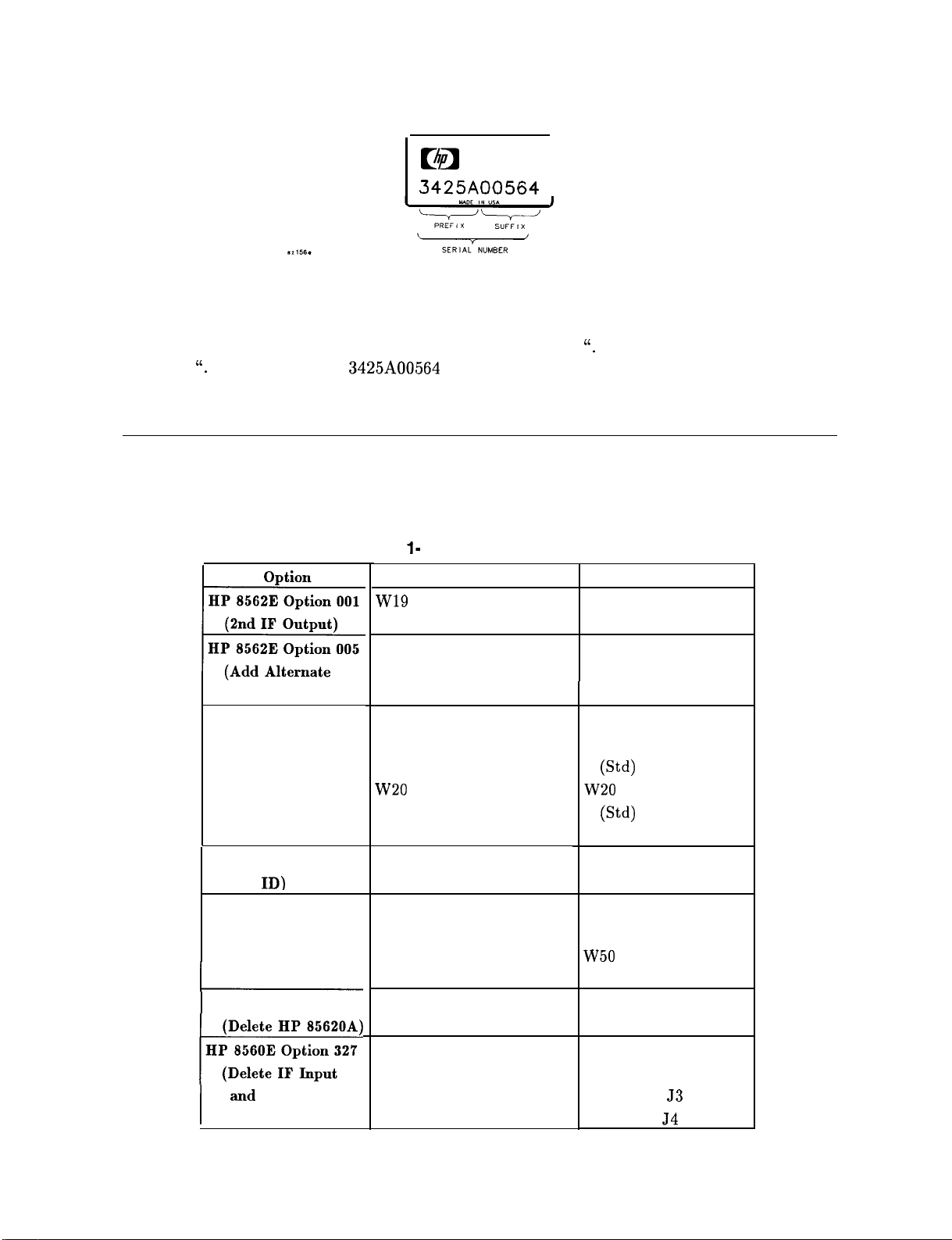
c!a
3425A00564
HEWLETT
PACKARD
I
Earlier Serial Number Label Example
The new serial number format (USOOOOOOOO) is always considered “above” the earlier format
(OOOOAOOOOO) h y
above” or “. . . .
w en ou encounter change information such as “. . . . serial prefix 3425A and
serial number
3425A00564
and above.”
Instrument Variations
There are options available to the HP 85623. The following table lists these options and
identifies the assemblies which are unique to them.
Table l- 1. Instrument Variations
Sweep Output)
HP 85623 Option 007
(Fast ADC)
HP 85623 Option 008
(SIG
ID)
HP 85623 Option 103
(Delete OCXO)
HP 85623 Option 104
and
Video Output)
Added
W19 Cable Assembly
Rear-Panel J 10
W58 Cable Assembly
Al6 Fast ADC Assembly
A3 Interface Assembly
(Opt 007)
W20 Cable Assembly
(Opt 007)
W59 Cable Assembly
Al5 RF Assembly (Opt 008)
Al5 RF Assembly (Opt 103)
Deleted
A3 Interface Assembly
Wd)
W20 Cable Assembly
(St4
Al5 RF Assembly (Std)
Al5 RF Assembly (Std)
W49 Cable Assembly
W50 Cable Assembly
A21 OCXO
HP 85620A Mass
Memory Module
W24 Cable Assembly
W36 Cable Assembly
Front-panel
Rear-panel
53
54
l-2 General Information
Page 26

HP 85629B Test and Adjustment Module
When attached to the rear panel of the spectrum
adjustment module (TAM) provides diagnostic functions for the HP 85623. The TAM is
accessed by a computer running interface software; this software is supplied with Option 915,
add Service Documentation. The TAM measures voltages at key points in the circuitry and
flags a failure whenever the voltage falls outside the limits. The TAM locates the failure
to a small functional area, which can then be examined manually. See chapter 7, “General
Troubleshooting,”
software.
for a complete description of how to use the TAM and its interface
amdyzer,
the HP 85629B test and
General Information
l-3
Page 27

Service Kit
The spectrum analyzer service kit (HP part number 08562-60021) contains service tools
required to repair the instrument. Refer to Table l-2 for a list of items in the service kit.
Table l-2. Service Kit Contents
Description
Cable Puller
PC Board Prop
Line Filter Assembly
Line Switch Cable
Extender Cable
BNC to SMB (snap-on) Cable
Connector Extractor Tool Kit
Quantity
I
1
1
1
1
1
2
I
HP Part Number
5021-6773
5021-7459
5061-9032
5062-0728
5062-0737
85680-60093
8710-1791
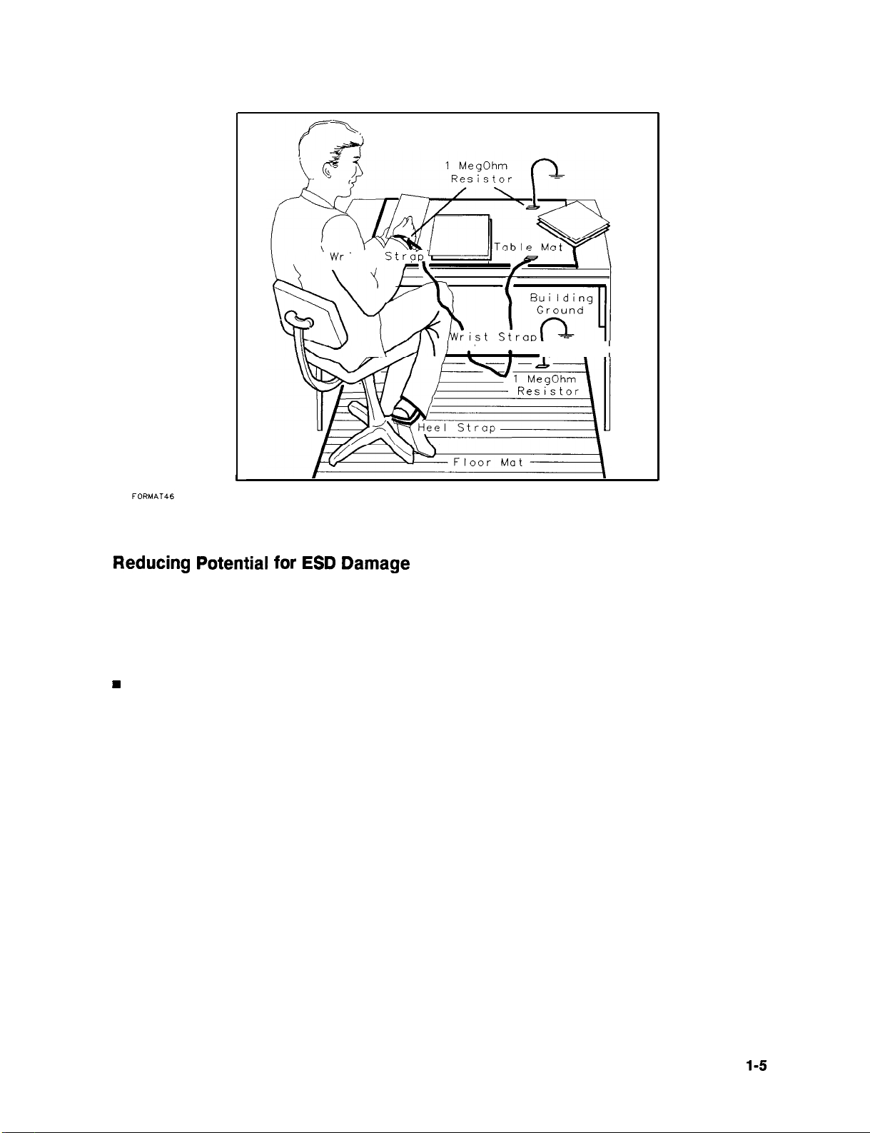
Electrostatic Discharge
Electrostatic discharge (ESD)
all work performed on assemblies consisting of electronic components should be done at a
static-free workstation. Figure l-l is an example of a static-safe workstation using two kinds
of ESD protection:
w
Conductive table mat and wrist-strap combination
n Conductive floor mat and heel-strap combination
These methods may be used together or separately.
can damage or destroy electronic components. Therefore,
l-4 General Information
Page 28
ist
Stra61
Building
Ground
w--A-
Cord
’
I-
L
II
Figure l-l. Example of a Static-Safe Workstation
Reducing Potential for ESD Damage
The suggestions that follow may help reduce ESD damage that occurs during instrument
testing and servicing.
n Before connecting any coaxial cable to an spectrum analyzer connector for the first time
each day, momentarily ground the center and outer connectors of the cable.
H
Personnel should be grounded with a resistor-isolated wrist strap before touching the center
pin of any connector and before removing any assembly from the unit.
n Be sure all instruments are properly earth-grounded to prevent build-up of static discharge.
General Information
l-5
Page 29
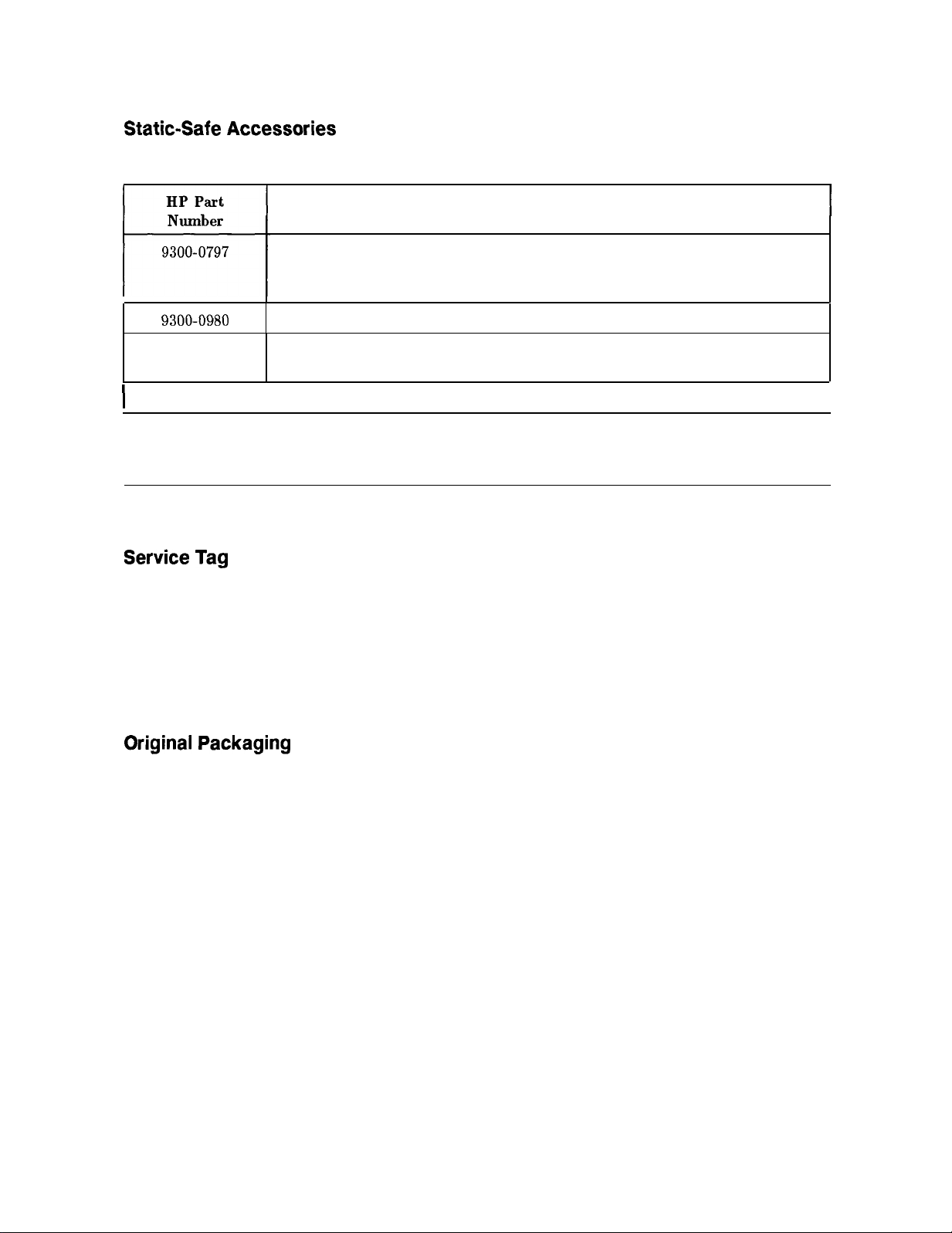
Static-Safe Accessories
Set includes: 3M static control mat 0.6 m x 1.2 m (2 ft x 4 ft) and 4.6 cm (15 ft)
ground wire. (The wrist-strap and wrist-strap cord are not included. They must
be ordered separately.)
Table 1-3. Static-Safe Accessories
Description
Wrist-strap cord, 1.5 m (5 ft).
Wrist-strap, color black, stainless steel, without cord, four adjustable links and
7 mm post-type connection.
ESD heel-strap (reusable 6 to 12 months).
I
I
9300-0980
9300-1383
9300-l 169
Returning Instruments for Service
Service Tag
If you are returning the instrument to Hewlett-Packard for servicing, fill in and attach a blue
service tag. Service tags are supplied in the back of this chapter.
Please be as specific as possible about the nature of the problem. If you have recorded any
error messages that appeared on the screen, or have completed a performance test record, or
have any other specific data on the performance of the spectrum analyzer, please send a copy
of this information with the unit.
Original Packaging
I
Before shipping, pack the unit in the original factory packaging materials if they are available.
If the original materials are unavailable, identical packaging materials may be acquired
through any Hewlett-Packard Sales and Service Office. Descriptions of the packaging materials
are listed in Figure 1-2.
1-6 General Information
Page 30

Other Packaging
Caution
Repackage the spectrum analyzer in the original packaging materials or with commercially
available materials described in steps 4 and 5, below.
1. Attach a completed service tag to the instrument.
2. Install the front-panel cover on the instrument.
3. Wrap the instrument in antistatic plastic to reduce the possibility of damage caused by
electrostatic discharge.
4. Use the original materials or a strong shipping container that is double-walled, corrugated
cardboard carton with 159 kg (350 lb) bursting strength. The carton must be both large
enough and strong enough to accommodate the spectrum analyzer and allow at least
3 to 4 inches on all sides of the spectrum analyzer for packing material.
5. Surround the equipment with at least 3 to 4 inches of packing material, or enough to
prevent the equipment from moving in the carton. If packing foam is unavailable, the best
alternative is SD-240 Air
Air Cap looks like a plastic sheet covered with
pink-colored Air Cap to reduce static electricity. Wrap the equipment several times in this
material to both protect the equipment and prevent it from moving in the carton.
Spectrum analyzer damage can result from using packaging materials other
than those specified. Never use styrene pellets in any shape as packaging
materials. They do not adequately cushion the equipment or prevent it from
shifting in the carton. They cause equipment damage by generating static
electricity and by lodging in the spectrum analyzer fan.
Cap
from Sealed Air Corporation (Commerce, CA 90001).
TM
l-1/4
inch air-filled bubbles. Use the
6. Seal the shipping container securely with strong nylon adhesive tape.
7. Mark the shipping container
handling.
8. Retain copies of all shipping papers.
“FRAGILE, HANDLE WITH CARE” to assure careful
General Information 1-7
Page 31

Item
Description
HP Part Number
I
1
2
r
Figure 1-2. Spectrum Analyzer Shipping Container and Cushioning Materials
1-6 General Information
3
9211-6969
9220-5073
9220-5072
Outer Carton
Pads (2)
Top Tray
Page 32

Recommended Test Equipment
Table l-4 lists the recommended test equipment required for operation verification,
performance tests, adjustments, troubleshooting, and the Test and Adjustment Module. Any
equipment that meets the critical specifications given in the table can be substituted for the
recommended model(s). Operation verification, and the performance tests are located in the
Calibration Guide.
General Information l-9
Page 33

Table l-4. Recommended Test Equipment
Instrument
sources
jynthesized sweeper
(two required)
;ynthesizer/level generator
iynthesized
signal generator
Critical Specifications
for Equipment Substitution
Frequency range:
10 MHz to 13.2 GHz
Frequency accuracy (CW): x
Leveling modes: Internal & External
Modulation modes: AM & Pulse
Power level range: -80 to
Frequency range: 200 Hz to 80 MHz
Frequency accuracy: 1 x
Flatness:
Attenuator accuracy:
External 10 MHz reference input
Frequency resolution: 1 Hz
Frequency range: 100
Residual SSB phase noise at 1 GHz:
<-73
<-lo7 dBc/Hz
<-124
<-124
f0.15
dBc/Hz
dBc/Hz
dBc/Hz
dB
<f0.09
at 10 Hz offset
at 1 kHz offset
at 10 kHz offset
at 100 kHz offset
+16
10e7/month
kHz
to 2.5 GHz
l0-g/day
dBm
dB
Xecommendec
Model
HP
8340A/B*
HP 83630A
opt 001, 008
HP 3335A+
HP 8663A
Use
PAT,
WV
PAT,
WV
p,v
‘&e/function generator
LM/FM signal generator
Part of microwave workstation
’ =
performance tests; A = adjustments; M = test & adjustment module; T = troubleshooting;
J =
operation verification
Frequency range: 10
Pulse width: 200 ns
3utput
amplitude: 5 V peak-to-peak
Functions: pulse & triangle
Pulse rise time: <lOO ns
I’TL sync output
Frequency range: 1 MHz to 200 MHz
Frequency modulation mode
Modulation oscillator frequency: 1 kHz
FM peak deviation: 5 kHz
kHz
to 50 MHz
HP 8116A
HP 8640B
HP 8642A
P,A
A
l-10
General Information
Page 34

Table 1-4. Recommended Test Equipment (continued)
Instrument
Counters
Frequency standard
Microwave frequency counter
Universal counter
Receivers
spectrum
analyzer Frequency range: 300 kHz to 7 GHz
Critical Specifications
for Equipment Substitution
Output frequency: 10 MHz
Accuracy: <l x
Frequency range: 9 MHz to 7 GHz HP 5343A OR
External frequency reference input HP 5350B*
Timebase accuracy (aging): <5 x
Modes: TI
Time interval measurement range: 100 ns to 120 s
Frequency count range: 400 Hz to 11 MHz
Frequency resolution: 1 mHz
Timebase accuracy (aging): <3 x
External 10 MHz reference input
Amplitude range: -70 dBm to
10-l’
lo-“/day
A+B,
frequency count HP
10m7/month
+20 dBm
Recommended
Model
HP 5061B
Option 001
5334A/B
HP 8566B*
Use
PA
PAT,
WV
P
A,T
VIeasuring
iensors
‘ower
‘ower sensor
‘ower sensor
receiver
sensor Frequency range: 10 MHz to 13.2 GHz
Compatible w/power sensors
dB relative mode
Resolution: 0.01 dB
Reference accuracy:
Maximum SWR:
1.40 (10 to 30 MHz)
1.18 (30 to 50 MHz)
1.10 (50 MHz to 2 GHz)
1.18 (2 to 13.2 GHz)
Frequency range: 250 MHz to 350 MHz
Power range: 100 nW to 10
Maximum SWR: 1.15 (250 to 350 MHz)
Frequency range: 100 kHz to 2.9 GHz
Maximum S WR:
1.1 (1 MHz to 2.0 GHz)
1.30 (2.0 GHz to 2.9 GHz)
<fl.2%
PW
HP
8902A*
HP 8481A+
HP 8481D
HP
8482A*
PAT,
WV
PAT,
WV
P,A
PAT,
WV
’
Part of microwave workstation
’ =
performance tests; A = adjustments; M = test & adjustment module; T = troubleshooting;
J =
operation verification
General Information l-l 1
Page 35

Table 1-4. Recommended Test Equipment (continued)
Instrument
Xher
Equipment
2ontroller
1scilloscope
Lmplifier
‘ower
supply Output voltage:
Required to run operation verification software.
No substitute.
Bandwidth (3
Two channels
Minimum vertical deflection factor: 55
Minimum
Digitizing display with time cursors
Delta-t cursor accuracy in 500
Frequency range: 2.0 to 8.0 GHz
Minimum output power (leveled)
2.0 to 8.0 GHz:
Output SWR (leveled):
Output voltage accuracy:
Critical Specifications
for Equipment Substitution
dB):
dc to 100 MHz
timebase
setting: <lOO ns
+16
dBm
<1.7
224
Vdc
<f0.2
ns/Div: <O.l ps
V
mV/div
Recommended
Model
HP
9816A,
HP
9836A/C,
HP 310,320
HP 332,360
HP 54501A*
HP 11975A
HP 6114A
Use
V
PAT
P
A
ignature
)igital
multimeter Clock frequency
Time interval function
voltmeter Range: -15 Vdc to
Accuracy:
Input impedance: 21 M
>lO
<fl
mV on 10 V range
MHz
+120
Vdc
D
?robes
)VM
test leads
ligh frequency probe
Part of microwave workstation
’ =
performance tests; A = adjustments; M = test & adjustment module; T = troubleshooting;
7 =
operation verification
236
inches, alligator clips, probe tips
No substitute
HP
5005A/B
HP
3456A*
HP 34118A
HP 85024A
T
A,T
A,T
T
1-12 General Information
Page 36

Table 1-4. Recommended Test Equipment (continued)
Instrument
Accessories
Directional bridge
Directional coupler
(two required)
10 dB step attenuator
1 dB step attenuator
Critical Specifications
for Equipment Substitution
Frequency range: 1 to 80 MHz
Coupling: 6 dB (nominal)
Maximum coupling deviation: <
Directivity: 40 dB minimum
Impedance: 50 R (nominal)
Frequency range: 2.0 to 8.1 GHz
Coupling: 16.0 dB (nominal)
Maximum coupling deviation: fl dB (nominal)
Directivity: 14 dB minimum
Flatness: 0.75 dB maximum
VSWR:
fnsertion
Attenuation range: 30 dB
Frequency range: dc to 80 MHz
Connectors: BNC(f)
Attenuation range: 12 dB
Frequency range: dc to 80 MHz
Connectors: BNC(f)
<1.45
loss:
<1.3
dB
1 dB (nominal)
Recommended
Model
HP 8721A
0955-0098
HP 355D
HP 355C
Use
P
P
p,v
p,v
20 dB fixed attenuator
10 dB fixed attenuator
Reference attenuator
* Part of microwave workstation
P = performance tests; A = adjustments; M = test & adjustment module; T = troubleshooting;
V = operation verification
Frequency range: dc to 13.2 GHz
Attenuation accuracy:
Maximum SWR: 1.2 (dc to 2.9 GHz)
Frequency range: dc to 13.2 GHz
Attenuation accuracy:
Maximum SWR: 1.2 (dc to 2.9 GHz)
Supplied with HP 8481D
<fl
<f0.6
dB
dB
HP 8491B
Option 020
HP 8491B
Option 010
HP 11708A
p,v
p,v
P,A
General Information
l-1
3
Page 37

Table 1-4. Recommended Test Equipment (continued)
Instrument
Termination
1
Low-pass filter
I
Jaw-pass
I
Jaw-pass
I
‘ower
s
iervice
7
Yuning
c
Zables
7
Test
C
:able, RG-214/U HP 11500A
C
:able
C
:able,
filter
(two required)
filter
(two required)
splitter
accessory kit
tool
cable
50 Sl coaxial
(jive required)
Frequency range: dc to 13.2 GHz
Impedance: 50
Maximum SWR:
Connector: Type N(m)
Cutoff frequency: 50 MHz
Rejection at 65 MHz:
Rejection at 75 MHz:
Cutoff frequency: 1.8 GHz
Rejection at >3 GHz:
0.1 dB ripple
Cutoff frequency: 4.4 GHz
Rejection at 5.5 GHz:
Frequency range: dc to 13.2 GHz
Output tracking:
insertion loss: 6 dB (nominal)
Equivalent output SWR:
No substitute
No substitute
Connectors: BNC(m)-to-SMB(f)
Length:
Connectors: Type N(m)
Length:
Connectors: SMA(m)
Length: 24 to 36 inches
?onnectors: BNC(m)
Length: 2 122 cm (48 in.)
Critical Specifications
for Equipment Substitution
52
<l.lO
>40
dB
>60
dB
>45
dB
>40
dB
<0.25
dB
<1.22
261
cm (24 in.)
291
cm (36 in.)
Recommendet
Model
HP
909A
0955-0306
0955-0491
HP 11689A
HP 11667B
08562-60021
8710-1010
85680-60093
8126-1578
HP 10503A
Use
P,M,V
P
P
A,T
A
AN
p,v
P
PAV
C
!able
(two required)
*
Part of microwave workstation
=
performance tests; A = adjustments; M = test & adjustment module; T = troubleshooting;
P
V= operation verification
rrequency
tiaximum SWR:
vlaximum
Yonuectors:
,ength: 2 61 cm (24 in.)
range: 30 Hz to 26.5 GHz
<1.4
at 26.5 GHz
insertion loss: 3 dB
APC 3.5(m), both ends
1-14 General Information
8120-4921
Page 38

Table 1-4. Recommended Test Equipment (continued)
Instrument
Cable, HP-IB
(eight required)
Adapters
Adapter
Adapter
(three required)
Adapter
Adapter
Adapter
Adapter
(two required)
Adapter
Adapter
Adapter
4dapter
(two required)
4dapter
(two required)
4dapter
4dapter
4dapter
4dapter
4dapter
4dapter
(two required)
4dapter
(two required)
4dapter
4dapter
4dapter
4dapter
4dapter
Critical Specifications
for Equipment Substitution
Required w/operation verification software
Required
Length: 2 m (6.6 ft.)
Type N(f)-to-BNC(m)
Type N(m)-to-BNC(f)
Type N(f)-to-BNC(f)
Type N(m)-to-N(m)
Type N(f)-to-APC 3.5(m)
Type N(m)-to-APC 3.5(m)
Type N(m)-to-APC 3.5(f)
Type N(m)-to-BNC(m)
Type N(m)-to-N(f)
Type N(f)-to-APC 3.5(f)
Type N(m)-to-SMA(f)
Type N(f)-to-SMA(f)
BNC(f)-to-BNC(f)
BNC tee(f)(m)(f)
BNC(f)-to-SMA(m)
BNC(f)-to-dual banana plug
APC 3.5(f)-to-APC 3.5(f)
APC 3.5(m)-to-APC 3.5(m)
2.4 mm(f)-to-2.4 mm(f)
APC 3.5(f)-to-2.4 mm(f)
APC 3.5(m)-to-2.4 mm(f)
Type N(f)-to-2.4 mm(f)
Type N(f)-to-2.4 mm(m)
w/HP
85629B test & adjustment module
Recommendec
Model
HP 10833B
1250-1477
1250-1476
125@1474
125G1475
1250-1750
1250-1743
125G1744
1250-1473
1250-1472
1250-1745
1250-1250
1250-1772
1250-0059 A
12560781
1250-1200
1251-2816
5061-5311
1250-1748
HP 11900B
HP 11901B
HP 11901D
HP 11903B
HP 11903C
Use
PAM
P,A
P,A,V
p,v
P
A
P,M,V
p,v
P
P
p,v
p,v
P
‘AM,\
PAV
A,T
P,M,V
p,v
‘,A,T,V
P
P
‘,.%T,V
P
’ Part of microwave workstation
’ =
performance tests; A = adjustments; M = test & adjustment module; T = troubleshooting;
J =
operation verification
General Information 1-15
Page 39

Sales and Service Offices
Hewlett-Packard has sales and service offices around the world providing complete support
for Hewlett-Packard products. To obtain servicing information, or to order replacement
parts, contact the nearest Hewlett-Packard Sales and Service Office listed in Table l-5. In
any correspondence, be sure to include the pertinent information about model numbers, serial
numbers, and assembly part numbers.
Note
Within the USA, a toll-free phone number is available for ordering
replacement parts. Refer to the section entitled, “Ordering Information” in
Chapter 5, “Replaceable Parts,”
for the phone number and more information.
1-16 General Information
Page 40

Table 1-5. Hewlett-Packard Sales and Service Offices
US FIELD OPERATIONS
Headquarters
Hewlett-Packard Co. Hewlett-Packard Co.
19320 Pruneridge Avenue 301 E. Evelyn
Cupertino, CA 95014 Mountain View, CA 94041
(800) 752-0900 (415) 694-2000
Colorado
Hewlett-Packard Co.
24 Inverness Place, East
Englewood, CO 80112
(303) 649-5512
New Jersey
Hewlett-Packard Co.
150 Green Pond Rd.
Rockaway, NJ 07866
(201)
5865400
California, Northern
Atlanta Annex
Hewlett-Packard Co.
2124 Barrett Park Drive
Kennesaw, GA 30144
(404) 648-0000
Texas
Hewlett-Packard Co.
930 E. Campbell Rd.
Richardson, TX 75081
(214) 231-6101
California, Southern
Hewlett-Packard Co.
1421 South Manhattan Ave.
Fullerton, CA 92631
(714) 999-6700
Illinois
Hewlett-Packard Co.
545 E. Algonquin Rd.
Arlington Heights, IL 60005
(847) 342-2000
EUROPEAN FIELD OPERATIONS
Headquarters
Hewlett-Packard S.A. Hewlett-Packard France
150, Route du Nant-d’Avri1 1 Avenue Du Canada Hewlett-Packard
1217 Meyrin 2/Geneva Zone
Switzerland
(41 22) 780.8111
France
D’Activite
F-91947 Les
France
(33 1) 69 82 60 60
UIis
De Courtaboeuf
Cedex
Germany
Hewlett-Packard GmbH
61352 Bad Homburg v.d.H
Germany
(49 6172) 16-O
Great Britain
Hewlett-Packard Ltd.
EskdaIe
Road, Winnersh Triangle
Wokingham, Berkshire RG41 5DZ
England
(44
734) 696622
Strasse
INTERCON
Headquarters
Hewlett-Packard Company
3495 Deer Creek Road
‘alo
Alto, California, USA
34304-1316
1415)
857-5027
China
China
Hewlett-Packard Company Hewlett-Packard Japan, Ltd.
$8 Bei
San Huan Xl Road
;huang Yu Shu Tokyo 192, Japan
Iai Dian District
3eijing,
China
86 1) 256-6888
Australia
Hewlett-Packard Australia Ltd.
31-41 Joseph Street
Blackburn, Victoria 3130
(61 3) 895-2895
Japan
9-l Takakura-Cho, Hachioji
(81 426) 60-2111
FIELD OPERATIONS
raiwan
Hewlett-Packard Taiwan
lth
Floor, H-P Building
137 Fu Hsing North Road
Taipei,
Taiwan
886 2) 712-0404
Canada
Hewlett-Packard (Canada) Ltd.
17500 South Service Road
Tram-Canada Highway
Kirkland, Quebec
Canada
(514) 697-4232
H9J 2X8
Singapore
Hewlett-Packard Singapore (Pte.) Ltd.
150 Beach Road
#29-00 Gateway West
Singapore 0718
(65) 291-9088
General Information 1-17
Page 41

2
Adjustment Procedures
Introduction
This chapter contains information on automated and manual adjustment procedures. Perform
the automated procedures using the HP 85629B test and adjustment module (TAM). Never
perform adjustments as routine maintenance. Adjustments should be performed after a repair
or performance test failure. Refer to Table 2-l to for which adjustments to perform.
Automated Procedures
Using the TAM
Front End Cal (adjustment)
Manual Procedures
1. High Voltage Power Supply Adjustment
2. Display Adjustment
3. IF
4. IF Amplitude Adjustments
5. DC Log Amplifier Adjustments
6. Sampling Oscillator Adjustment
7. YTO Adjustment
8. LO Distribution Amplifier Adjustment
9. Frequency Response Adjustment
10. Calibrator Amplitude Adjustment
11. 10 MHz Reference Adjustment-OCXO
12. 10 MHz Reference Adjustment-TCXO (Option 103)
13. Demodulator Adjustment
14. External Mixer Bias Adjustment
15. External Mixer Amplitude Adjustment
16. YIG-Tuned Filter/Mixer (RYTHM) Adjustment
17. 16 MHz PLL Adjustment
18. 600 MHz Reference Adjustment
Bandpass
Adjustment
Note
Before performing any adjustments, allow the spectrum analyzer to warm up
for at least 5 minutes.
Adjustment Procedures 2-1
Page 42

Safety Considerations
Although this instrument has been designed in accordance with international safety standards,
this manual contains information, cautions, and warnings which must be followed to ensure
safe operation and to prevent damage to the instrument. Service and adjustments should be
performed only by qualified service personnel.
w
Warning
Adjustments in this section are performed with power supplied to the
instrument and protective covers removed. There are voltages at many points
in the instrument which can, if contacted, cause personal injury. Be extremely
careful. Adjustments should be performed only by trained service personnel.
w
Power is still applied to this instrument with the (LINE) switch in the off
position. Before removing or installing any assembly or printed circuit board,
remove the line-power cord.
w
Capacitors inside the instrument may still be charged, even if the instrument
has been disconnected from its source of supply.
n
Use a nonmetallic adjustment tool whenever possible.
Which Adjustments Should Be Performed?
Table 2-l lists the manual adjustments that should be performed when an assembly is repaired
or changed. It is important to perform the adjustments in the order indicated to ensure that
the instrument meets its specifications.
Test Equipment
The equipment required for the manual adjustment procedures is listed in Table 1-4,
“Recommended Test Equipment
given in the table may be substituted for the preferred test equipment.
Any equipment that satisfies the critical specifications
.”
Adjustable and Factory-Selected Components
Table 2-2 lists the adjustable components by reference designation and name. For each
component, the table provides a description and lists the adjustment number.
Refer to Table 2-3 for a complete list of factory-selected components used in the instrument
along with their functions. Factory-selected components are identified with an asterisk on the
schematic diagrams.
2-2 Adjustment Procedures
Page 43

Adjustment Tools
For adjustments requiring a nonmetallic tuning tool, use fiber tuning tool, HP part number
8710-0033.
Two different tuning tools may be necessary for IF
the type of tuning slug used in the slug-tuned inductors. If the tuning slug requires a slotted
tuning tool, use HP part number 8710-1010. If the tuning slug requires a forked tuning tool,
use HP part number 8710-0772.
Never try to force an adjustment control. This is especially critical when tuning variable
capacitors or slug-tuned inductors. Required service accessories, with part numbers, are listed
under “Service Kit” in Chapter 1, “General Information.”
bandpass
adjustments, depending upon
Instrument Service Position
Refer to Chapter 4, “Assembly Replacement ,”for information on removing the spectrum
analyzer cover assembly and accessing all internal assemblies.
Adjustment Procedures 2-3
Page 44

Table 2-1. Related Adjustments
Assembly Changed
or Repaired
AlAl
keyboard
AlA
RPG
A2 controller
A3 interface
A4 log
A5 IF
A6 power supply
A6Al
A7 switched LO
amp/Cal
HV module
distribution amplifiei
osc
Perform the following related adjustments in the order listed
!Io
related adjustment
vo related adjustment
16 MHz PLL adjustment
Display adjustment
[f
EEROM from old A2 controller could not be used in
new A2 or if EEROM must be replaced, also perform
the following adjustments:
LO distribution amplifier adjustment
External mixer amplitude adjustment
YIG-tuned filter/mixer adjustment
Frequency response adjustment
Display adjustment (fast zero span)
Frequency response adjustment
Display adjustment (Fast Zero Span)
Demodulator adjustment
1F
amplitude adjustment
DC log amplifier adjustment
1F bandpass
[F
amplitude adjustment
High voltage power supply adjustment
Display adjustment
High voltage power supply adjustment
Display adjustment
LO distribution amplifier adjustment
Frequency response adjustment (or perform the
frequency response performance test in the
HP 8560 E-Series Spectrum Analyzer Calibration Guide.
The adjustment must be performed if the performance test fails.:
adjustment
4djustment
Number
17
2
8
15
16
9
2
9
2
13
4
5
3
4
1
2
1
2
8
9
2-4 Adjustment Procedures
Page 45

Table 2-1. Related Adjustments (continued)
Assembly Changed
or Repaired
A8 low band mixer
A9 input attenuator
A10 RYTHM
All YTO
Al3 2nd converter
Al4 frequency control
Al5 RF
A15UlOO
sampler
Perform the following related adjustments in the order listed
Frequency response adjustment
Frequency response adjustment (or perform the
frequency response performance test in the
HP 8560 E-Series Spectrum Analyzer Calibration Guide.
The adjustment must be performed if the performance test fails
YIG-tuned filter/mixer (RYTHM) adjustment
Frequency response adjustment
YTO adjustment
Frequency response adjustment
Display adjustment (fast zero span)
YTO adjustment
LO distribution amplifier adjustment
Frequency response adjustment
10 MHz reference adjustment (TCXO, Option 103)
600 MHz reference adjustment
Calibrator amplitude adjustment
External mixer bias adjustment
Sampling oscillator adjustment
External mixer amplitude adjustment
Frequency response adjustment
Sampling oscillator adjustment
Adjustment
Number
9
9
16
9
7
9
2
7
8
9
12
18
10
14
6
15
9
6
Al7 CRT driver
A18Vl
CRT
A19 HP-IB
A21 OCXO
Display adjustment
Display adjustment
No related adjustment
10 MHz reference adjustment (OCXO)
2
2
11
Adjustment Procedures 2-5
Page 46

Table 2-2. Adjustable Components
Reference
Designator
A2R152
A2R206
A2R209
A2R215
A2R218
A2R262
A2R263
A2R268
A2R271
A4C707
A4R445
A4R531
A4R544
A4R826
A5L300
A5L301
A5L700
A5L702
A5R343
A5T200
A5T202
Adjustment
Name
16 MHz PLL ADJ
DGTL X GAIN
SWEEP OFFSET
DGTL Y GAIN
VIDEO OFFSET
STOP BLANK
START BLANK
VIDEO GAIN
SWEEP GAIN
FM DEMOD
LIMITER PHASE
LOG AMP TOS
LIN FIDELITY BOW
CAL OSC AMPTD
LC CTR 1
LC CTR 2
LC CTR 3
LC CTR 4
15 DB ATT
XTAL CTR 1
XTAL CTR 2
Adjustment
Number
17
2
2
2
2
2
2
2
2
13
5
5
5
4
3
3
3
3
4
3
3
Description
Adjusts the free-running frequency of the
16 MHz CPU clock.
Adjusts the horizontal gain in the X line generator.
Adjusts the beginning of the trace to the leftmost
vertical graticule line in fast-analog zero-span mode.
Adjusts the vertical gain in the Y line generator.
Adjusts the vertical position in fast-analog zero
span to match the digital zero-span input.
Adjusts the blanking at the end of a vector on
the display.
Adjusts the blanking at the start of a vector on
the display.
Adjusts the vertical gain in fast-analog zero span
to match with the digital zero-span input.
Adjusts the end of the trace to the rightmost
vertical-graticule line in fast-analog
zero-span mode.
Adjusts the FM demodulation for a peak response.
Adjusts Limiter Phase for peak response.
Minimizes error to Top of Screen.
Minimizes Linearity Fidelity error.
Sets calibration oscillator output power
(nominally -35
the IF during the AUTO IF ADJUST routines.
Adjusts center frequency of first stage of LC
bandwidth filter to 10.7 MHz.
Adjusts center frequency of second stage of LC
bandwidth filter to 10.7 MHz.
Adjusts center frequency of third stage of LC
bandwidth filter to 10.7 MHZ.
Adjusts center frequency of fourth stage of LC
bandwidth filter to 10.7 MHz.
Adjusts the attenuation of the reference 15 dB
attenuator for 15 dB between minimum and
maximum attenuation.
Adjusts center frequency of first stage of crystal
bandwidth filter to 10.7 MHZ.
Adjusts center frequency of second stage of crystal
bandwidth filter to 10.7 MHZ.
dBm).
This power is injected into
2-6 Adjustment Procedures
Page 47

Table 2-2. Adjustable Components (continued)
Reference
Designator
A5T500
A5T502
A6R410
A14R42 6.01 GHz
A14R76
A14R93
A15ClOO
A15C210
A15C750 vcxo
A15C751
A15U302
A15R561
A15R926
A17R4
A17Rll
A17R21
A17R26
A17R34
A17R55
A17R57
A17R75
A17R77
A17R90
A17R92
A17R93
Adjustment
Name
XTAL CTR 3
XTAL CTR 4
HV ADJ
FM SPAN
3.2 GHz
SMPL MATCH
VCO RANGE
TRIPLER
10 MHz ADJ
CAL AMPTD
EXT BIAS ZERO
2
GAIN
CUTOFF
Z FOCUS
X FOCUS
COARSE FOCUS
X GAIN
X POSN
Y GAIN
Y POSN
TRACE ALIGN
DDD
ASTIG
Adjustment
Number
3
3
1
7
7
7
6
6
18
18
12
10
14
2
2
2
2
2
2
2
2
2
2
2
2
Description
Adjusts center frequency of third stage of crystal
bandwidth filter to 10.7 MHz.
Adjusts center frequency of fourth stage of crystal
bandwidth filter to 10.7 MHz.
Adjusts the voltage between A6TP405 and A6TP401
to the voltage marked on the
module.
Adjusts the main coil tune driver current at a
YTO frequency of 6.01 GHz (near the upper YTO
frequency limit).
Adjusts the FM span accuracy by affecting the
sensitivity of the FM coil driver.
Adjusts the main coil fixed driver current at a
YTO frequency of 3.2 GHz (near the lower
YTO frequency limit).
Transforms the sampler input impedance to 50 ohms
over the 285 to 297.2 MHz range.
Adjusts the VCO tank capacitance so that 21V
on the VCO tune line equals 298 MHz VCO frequency.
Adjusts for maximum 600 MHz reference output.
Adjusts for maximum 600 MHz reference output.
Adjusts frequency of the temperature
compensated crystal oscillator (TCXO) to 10 MHz.
Adjusts amplitude of the 300 MHz calibrator signal
to -10.0
Adjusts zero bias point of external mixer bias.
Adjusts maximum intensity.
Adjusts intensity to turn off blanked lines.
Adjusts focus for lines of different brightness.
Adjusts focus at the left and right corners of the display.
Adjusts focus at the center of the display.
Adjusts the horizontal-deflection amplifier gain.
Adjusts the CRT horizontal position.
Adjusts the vertical-deflection amplifier gain.
Adjusts the CRT vertical position.
Adjusts the display axis rotation.
Adjusts focus of the center of the display.
Adjusts for the spot roundness on the CRT display.
dBm.
A6Al
high voltage
Adjustment Procedures 2-7
Page 48

Table 2-3. Factory Selected Components
Reference
Designator
A5C204
A5C216
A5C326
A5C327
A5C505
A5C516
A5C717
A5C718
Adjustment
Number
3
3
3
3
3
Basis of Selection
Selected to optimize center frequency of LC tank that loads the crystal.
Selected to optimize center frequency of LC tank that loads the crystal.
Selected to optimize LC pole center frequency.
Selected to optimize LC pole center frequency.
Selected to optimize center frequency of LC tank that loads the crystal.
Selected to optimize center frequency of LC tank that loads the crystal.
Selected to optimize LC pole center frequency.
Selected to optimize LC pole center frequency.
2-6 Adjustment Procedures
Page 49

Using the TAM
The HP 85629B TAM, in conjunction with the HP
(TAM I/F SW), can be used to perform approximately half of the spectrum analyzer
adjustment procedures. Table 2-4 lists the TAM adjustments and their corresponding manual
adjustments. Refer to Chapter 7, “General Troubleshooting,” for information on loading and
running the TAM I/F SW.
The TAM adjustments do not include procedures for choosing factory-selected components. If
an adjustment cannot be made and a factory-selected component must be changed, refer to
the corresponding manual adjustment.
To select an adjustment, press
Position the pointer next to the desired adjustment using either the knob or step keys. Press
EXECUTE,
then follow the instructions displayed on-screen.
(m)
to display the TAM main menu, then press
8562E/TAM
Interface Software
AMUST.
Test Equipment
During the TAM adjustments, instructions for setting test equipment controls are displayed.
Table 2-5 lists the test equipment needed to perform each TAM adjustment. Required models
must be used. Substitutions may be made for recommended models. Substitute sources
must operate over the frequency ranges indicated. Recommended substitutes are listed in
the configuration menu. If you must substitute the source with a user-defined model, the
adjustments run faster using a synthesized source rather than an unsynthesized source.
Note
When connecting signals from the HP
to the adjustment, setup, use a high-frequency test cable with minimum
attenuation to 26.5 GHz. HP part number 8120-4921 is recommended for its
ruggedness, repeatability, and low insertion loss.
8340A/B
(or any microwave source)
Adjustment Indicator
To aid in making adjustments, the TAM displays an
the left-hand side of the display. A horizontal line moves inside the box to represent the
needle of an analog voltmeter. A digital readout appears below the box. Tick marks are often
displayed on the inside edges of the box indicating the desired needle position. (The tick
marks and needle are intensified when the needle is within this acceptable region.) During
some adjustments, an arrow appears along the right edge of the box. This arrow always
indicates the highest position the needle has reached. The arrow is useful when a component
must be adjusted for a peak response; if the peak is overshot, the arrow indicates where the
peak was. The component can be readjusted until the needle is at the same position as the
arrow.
“Analog Voltmeter Display Box” along
Adjustment Procedures
2-9
Page 50

Table 2-4. TAM Adjustments
TAM Adjustment
1. IF bandpass, LC poles
2. IF bandpass, crystal poles
3. IF amplitude
4. Limiter phase
5. Linear fidelity
6. Log fidelity
7. Sampling oscillator
8. YTO
9. LO distribution amplifier
10. Low band flatness*
11. High band flatness and YTF*
12. Calibrator amplitude
13. 10 MHz reference oscillator
14. External mixer bias
15. External mixer amplitude
‘These TAM adjustments are not compatible with the HP 85623.
Either perform the manual adjustment, or use the frequency response
adjustment software described in Chapter 3, “Frequency Response Adjustment Software.”
Corresponding
IF
bandpass
IF
bandpass
IF amplitude adjustment
DC log amplifier adjustments, A4 limiter phase
DC log amplifier adjustments, A4 linear fidelity
DC log amplifier adjustments, A4 log fidelity
Sampling oscillator adjustment
YTO adjustment
First LO distribution amplifier adjustment
Frequency response adjustment
Frequency response adjustment
YIG-tuned filter/mixer adjustment
Calibrator amplitude adjustment
10 MHz reference adjustment - TCXO
External mixer bias adjustment
External mixer amplitude adjustment
adjustment
adjustment
(Option 103)
Manual Adjustment
Adjustment
Number
3
3
4
5
5
5
6
7
8
9
9
16
10
12
14
15
,
2-10 Adjustment Procedures
Page 51

Table 2-5. Required Test Equipment for TAM
10. Low band flatness
11. High band flatness
12. Calibrator amplitude Power meter
13. 10 MHz reference
Oscillator (9 to 11 MHz)
14. External mixer bias
15. External mixer amplitude Power meter HP 8902A, HP 436A,
Not applicable
Power sensor (300 MHz) HP 8482A,
HP 8481A
Frequency counter
Manual probe cable
Power sensor HP 8481D, HP 8484A
(310.7 MHz, -25 to -35
Source (310.7 MHz, -30
dBm)
dBm)
5001-
8743
Not Applicable
HP 8902A, HP
HP 438A
HP 5342A, HP 5343A
HP 438A
HP
8340A/B
436A,
Adjustment Procedures
2-l
1
Page 52

Front End Cal (adjustment)
This procedure automates two manual procedures:
YIG-Tuned Filter/Mixer (RYTHM) Adjustment. This procedure is described in Chapter 3,
“Frequency Response Adjustment Software.”
Frequency Response Adjustment, and
2-12 Adjustment Procedures
Page 53

1. High Voltage Power Supply Adjustment
1. High Voltage Power Supply Adjustment
Assembly Adjusted
A6 power supply
Related Performance Test
There is no related performance test for this adjustment.
Description
The high voltage power supply is adjusted to the voltage marked on the
The
A6Al
HV module is characterized in the factory to ensure that the display filament
voltage is set to 6.0 V rms when the
+llO
Vdc (
nominal) supply is set to the voltage marked
on the HV module.
n
Warning
To minimize shock hazard, use a nonmetallic adjustment tool when adjusting
the A6 power supply.
n
The following procedure probes voltages that, if contacted, could cause
personal injury or death.
w
Note
Adjustment of the high voltage power supply should not be a routine
maintenance procedure. Any adjustments should be done only if the A6
power supply,
A6Al
HV module, or
A18Vl
CRT (display) is repaired or
replaced.
n You must perform the display adjustments after this adjustment if either the
display or HV module has been replaced.
PO%= A6TP405
A6Al
HV module.
DIGITAL VOLTMETER
fEz*-
Figure 2-1. High Voltage Power Supply Adjustment Setup
DVM TEST LEADS
SPECTRUM ANALYZER
J
SK1 1
Adjustment Procedures 2-13
Page 54

1. High Voltage Power Supply Adjustment
Equipment
Digital multimeter . . . . . . . . . . . . . . . . . . . . . . . . . . . . . . . . . . . . . . . . . . . . . . . HP 3456A
DVMtestleads
. . . . . . . . . . . . . . . . . . . . . . . . . . . . . . . . . . . . . . . . . . . . . . . . HP 34118A
Procedure
Warning
1. Turn the spectrum analyzer off by pressing
remove the spectrum analyzer cover. Fold down the A2 controller, A3 interface, A4 log
amplifier/Cal oscillator, and A5 IF assemblies. Remove the A6 power supply cover.
2. Position the spectrum analyzer as shown in Figure 2-l. Connect the positive DVM lead to
A6TP405
3. Set the HP 3456A controls as follows:
Function
Range
4. Reconnect the power cord to the spectrum analyzer and press
5. Record the voltage marked on the
6. Adjust A6R410 HV ADJ for a voltage equal to the voltage recorded in step 5.
7. Press
30 seconds for the high voltage power supply capacitors to discharge.
ILINE)
After disconnecting the ac power cord, allow capacitors in the high voltage
supply to discharge for at least 30 seconds before removing the protective
cover from the A6 power supply.
LuNE].
Disconnect the power cord and
and the negative DVM lead to
....................................................
.....................................................
A6Al
to turn the spectrum analyzer off and disconnect the power cord. Wait at least
A6TP401.
m
to the on position.
HV module.
Voltage marked on A6Al HV Module
DCVOLTS
1OOOVOLTS
=
Vdc
8. Disconnect the DVM test leads from
cover.
2-14 Adjustment Procedures
A6TP401
and
A6TP405.
Reinstall the power supply
Page 55

2. Display Adjustment
Assembly Adjusted
A2 controller
Al7 CRT driver
Related Performance Test
2. Display Adjustment
Sweep Time Accuracy (Sweep Times
<30
ms)
Description
Coarse adjustment of the deflection amplifiers, Z-axis amplifiers, and line generators is done
using the CRT adjust pattern. Fine adjustments use the graticule. The fast zero-span
amplitude adjustments correct for differences between analog and digital display modes. The
displayed sweep time accuracy is adjusted in the fast zero-span sweep adjustments.
SPECTRUM
ANALYZER
SK12
Figure 2-2. Display Adjustment Setup
Equipment
10 dB VHF step attenuator . . . . . . . . . . . . . . . . . . . . . . . . . . . . . . . . . . . . . . . . HP 355D
Adapters
Type N (m) to BNC (f) . . . . . . . . . . . . . . . . . . . . . . . . . . . . . . . . . . . . . . . . . . . 1250-1476
Cables
BNC, 122 cm (2 required)
. . . . . . . . . . . . . . . . . . . . . . . . . . . . . . . . . . . . . . . HP 10503A
Adjustment Procedures 2-15
Page 56

2. Display Adjustment
Procedure
Note
1. Turn the spectrum analyzer off by pressing (LINE). Remove the spectrum analyzer cover
and fold out the A2 controller and A3 interface assemblies as illustrated in Figure 2-2.
Connect the CAL OUTPUT to the INPUT. Adjustment locations are shown on the CRT
neck for Al7 adjustments and in Figure 2-4 for the A2 adjustments.
Perform the 16 MHz PLL Adjustment in this chapter before proceeding with
this adjustment.
Preliminary Adjustments
2. Set A17R55 X GAIN, A17R75 Y GAIN, A17R92 DDD, A17R93 ASTIG, A2R206 DGTL
X GAIN, A2R215 DGTL Y GAIN, A2R262 STOP BLANK, and A2R263 START
BLANK to midrange. Also set the rear-panel X POSN, Y POSN, and TRACE ALIGN to
midrange.
3. Set A17R21 Z FOCUS, A17R26 X FOCUS, and
4. Set A17R4 Z GAIN fully clockwise.
5. Turn the spectrum analyzer on and allow it to warm up for at least 3 minutes. Adjust
A17Rll
possible focus.
CUTOFF until the display is visible and A17R34 COARSE FOCUS for best
A17Rll
CUTOFF to midrange.
Cutoff Adjustment
6.
Press
(PRESET),
FOCUS, 127
until the retrace line between the bottom of trace A and the annunciators at the bottom
of the display just disappears.
(DISPLAY),
[ENTER),
STORE
IImNSITY
FOCTJS,
, 255
then GRAT OM OFF (OFF). Adjust
(ENTER),
STORE
IIfTEMSITY
, MORE 1 of 2,
A17Rll
CUTOFF
Deflection Adjustments
7.
Press
8. Refer to Figure 2-3 for locating the lines used for adjusting DGTL X GAIN and DGTL Y
9. Adjust A2R206 DGTL X GAIN until the two vertical lines near the left edge of the
10. Adjust A2R215 DGTL Y GAIN until the two horizontal lines near the top edge of the
11. Adjust A2R262 STOP BLANK and A2R263 START BLANK for the sharpest corners of
GRAT
ON OFF (ON),
ICAL), MO&F, I
the adjustments on the A2 controller assembly.
GAIN. Each of these lines is actually two lines adjusted for coincidence. The two lines will
form an “X” if they are not adjusted properly.
display converge to one single line.
display converge to one single line.
the outer box in the test pattern. The intensity of the corners should be the same as the
middle of the lines between the corners.
of 2 , and CRT
MORE
2 of 2 , INTENSITY, 80 (ENTER), STORE
ADJ
PATTERN . Fold up the A3 interface assembly to access
INmSITY
,
2-16 Adjustment Procedures
Page 57

2. Display Adjustment
12. Adjust the rear-panel TRACE ALIGN
until the leftmost line of the test pattern is parallel
with the CRT bezel. See Figure 2-3.
13. Adjust the rear-panel X POSN and A17R55 X GAIN until the leftmost
and the
14. Adjust the rear-panel Y POSN and A17R75 Y GAIN until the
softkey
labels appear just inside the left and right edges of the CRT bezel.
softkey
“@”
labels align with
their appropriate softkeys.
15. Press
[PRESET).
If necessary, readjust STOP BLANK and START BLANK for the
best-looking intersection of the graticule lines. This will be most noticeable along the
center vertical and horizontal graticule lines.
DEFLECTION ADJUSTMENTS
Adjust START BLANK
and STOP BLANK for
sharp corners
Adjust DGTL Y GAIN
until only one
line appears
/
/
characters
Adjust
DGTL X GAIN
until only one
line appears
Adjust TRACE ALIGN
to place this line
parallel to left
edge of CRT bezel
\ I
V
Adjust MIN
until dots in these
areas just disappear
Figure 2-3. CRT Adjust Pattern
INTEN
SOFTKEY
SOFTKEY
SOFTKEY
SOFTKEY
SOFTKEY
1
2
3
4
5
EXIT
SK13
Adjustment Procedures 2-17
Page 58

2. Display Adjustment
Intensity Adjustments
16.
Press
(AMPLITUDE)
should almost completely fill the screen with the noise floor. Press
A17R4 2 GAIN until the intensity at the center of the screen is about medium. It
should be fully illuminated, but not so bright that it burns the screen (15
photometer/radiometer).
then set the
REF LVL
to -70 dB and the LOG
d&‘DIV
(SGL).
to 1. This
Adjust
NITS
on a
17. Press (CAL), MORE I of 2 , and CRT
HP logo. Adjust A17R93 ASTIG for the smallest round dot possible.
18. Adjust A17R34 COARSE FOCUS and A17R92 DDD for the best focus of the characters
at the center of the screen.
19. Adjust A17R21 Z FOCUS for the best focus of the test pattern outside box.
20. Adjust A17R26 X FOCUS for best focus of the
pattern.
21. Repeat steps 17 through 20 to obtain the best overall focus quality.
ADJ
PATTERN. Locate the dot just below the
“0”
characters at the corners of the test
2-18 Adjustment Procedures
Page 59

2. Display Adjustment
AZR206
DGTLY GAIN
A2R215
DGTLY
GAlN
A2R263
START BLANK
AZR262 AZR268
STOP BLANK
VIDEO GAIN
SK14
Figure 2-4. A2 Display Adjustment Locations
Fast Zero Span Adjustments
22. Set A2R209 SWEEP OFFSET, A2R218 VIDEO OFFSET, and A2R268 SWEEP GAIN
to midrange. Adjustment locations are shown in Figure 2-4 for these A2 adjustments.
23. Set the HP 355D to 30 dB attenuation.
24. Press
(PRESET)
on the spectrum analyzer,
Figure 2-2. Set the spectrum analyzer controls as follows:
Centerfrequency
Span
. . . . . . . . . . . . . . . . . . . . . . . . . . . . . . . . . . . . . . . . . . . . . . . . . . . . . . . . . . . . OHz
Reference level
Resolution bandwidth
Videobandwidth
Sweep time
. . . . . . . . . . . . . . . . . . . . . . . . . . . . . . . . . . . . . . . . . . . .
. . . . . . . . . . . . . . . . . . . . . . . . . . . . . . . . . . . . . . . . . . . . . . . -40
. . . . . . . . . . . . . . . . . . . . . . . . . . . . . . . . . . . . . . . . . . . . 1 kHz
. . . . . . . . . . . . . . . . . . . . . . . . . . . . . . . . . . . . . . . . . . . . . . .
. . . . . . . . . . . . . . . . . . . . . . . . . . . . . . . . . . . . . . . . . . . . . . . . . . . . . 50ms
and connect the equipment as shown in
..300MHz
dBm
300Hz
Adjustment Procedures 2-19
Page 60

2. Display Adjustment
25. Press
26.
27. Set the sweep time to 10 ms.
(MKR), [m),
MARKER
MARKER-, REF
Press
(SAVE), SAVE STATE
LVL
again.
4
,and
REF
LYL. If the marker is not at the top graticule, press
STATE 0.
28. Press
29. Adjust A2R209 SWEEP OFFSET to place the beginning of the trace at the leftmost
30. Adjust A2R271 SWEEP GAIN to place the end of the trace at the tenth vertical graticule
31. Press
32.
33.
34.
35.
36. Adjust A2R209 and A2R271 until the start of sweep is aligned to the leftmost vertical
37. Press STATE 2 and STATE 3. The two traces should be aligned within
(SAVEI,
vertical graticule line.
line (one division from the right edge of the graticule).
Press
Set the sweep time to 50 ms. Press
Press
Switch between STATE 1 and STATE 2. Adjust A2R268 and A2R218 so that the trace in
state 1 is lined up with the top line of the graticule and the state 2 trace is lined up with
the eighth graticule down from the top (counting the top line). Repeat until the traces
align to within f0.2 divisions.
graticule line and the end of the sweep is aligned with the right most vertical graticule
line.
SAVE STATE
6-1
(SAVE),
SAVE STATE
and press the @) key seven times.
,and
,and
STATE
STATE
ISAVE),
[RECALL), RECALL STATE
,and
1.
2.
SAVE STATE, and STATE 3.
STATE
1.
4~0.1
divisions.
38.
Press STATE 0 and STATE
2-20 Adjustment Procedures
1
. The two traces should be aligned within fO.l divisions.
Page 61

3. IF
Bandpass
Adjustment
3. IF
Bandpass
Adjustment
Assembly Adjusted
A5 IF assembly
Related Performance Test
Resolution bandwidth accuracy and selectivity
Description
The center frequency of each IF
diodes and an inductor (for the LC poles) or a transformer (for the crystal poles). The
inductors and transformers are for coarse tuning and the varactors are for fine tuning by the
microprocessor. The inductors and transformers are adjusted such that the varactor diodes
are biased near the middle of their capacitance range. The varactor diode bias is measured
with the DVM.
Note
This procedure is not a routine adjustment. It should be performed only
if repairs to the A5 IF assembly are made. If the entire A5 IF assembly is
replaced, the assembly arrives pre-adjusted from the factory and requires no
further adjustment.
bandpass
filter pole is adjusted by DAC-controlled varactor
SPECTRUM
ANALYZER
5if BOARD
A3
-
A2
Figure 2-5. IF Bandpass Adjustment Setup
Equipment
Digital voltmeter
DVMtestleads
Special tuning tool (for slot-type tuning slugs)
Special tuning tool (for fork-type tuning slugs)
................................................
................................................
DVM
TEST LEADS
DIGITAL VOLTMETER
.......................
.......................
I
SK15
HP 3456A
HP 34118A
8710-1010
8710-0772
Adjustment Procedures 2-21
Page 62

3. IF
Bandpass
Procedure
Adjustment
1. Turn the spectrum analyzer off by pressing
@.
Disconnect the power cord. Remove the
spectrum analyzer cover and fold down the A2 controller, A3 interface, A4 log amp, and
A5 IF assemblies. Reconnect the power cord. Turn the spectrum analyzer on and allow it
to warm up for at least 30 minutes.
2. Connect the negative DVM lead to pin 6 of
A5J6.
See Figure 2-5 and Figure 2-6. Set the
HP 3456A controls as follows:
Function . . . . . . . . . . . . . . . . . . . . . . . . . . . . . . . . . . . . . . . . . . . . . . . . . . . DCVOLTS
Range . . . . . . . . . . . . . . . . . . . . . . . . . . . . . . . . . . . . . . . . . . . . . . . . . . . . . . . . . . . 1OV
3. On the spectrum analyzer press,
(-1,
l=),
2,
LMHz), ICAL),
and IF
AD3
IX OFF so
OFF is underlined.
PIN 2
. . l . . . . . PIN 16
PIN 1 n . . .
l .m
Figure 2-8. TAM Connector Pin Locations
LC Bandpass Adjustments
SP114E
4.
On the spectrum analyzer, press
AD3
CURR IF STATE.
message to disappear before continuing with the next step.
5. Read the voltage on
less than
+6.26
t6.06
Vdc, turn LC CTR 1 counterclockwise.
A5TP5
(thisis an empty-hole type of test point). If the voltage is
Vdc, turn A5L300 LC CTR 1 clockwise. If the voltage is greater than
6. Repeat steps 4 and 5 until the voltage reads i-6.16 Vdc
Note
If the range for the LC CTR adjustment is insufficient, replace the
appropriate factory-selected capacitor as listed in Table 2-6. To determine
the correct replacement value, center the LC CTR adjustment and press
AD3 CURR
IF STATE. After the IF ADJUST STATUS message disappears, read
the DVM display. Choose a capacitor value from Table 2-7, based on the
DVM reading and the presently loaded capacitor value. Table 2-10 lists a few
capacitor part numbers.
Caution
Turn the spectrum analyzer off by pressing luNE) to the off position before
removing or replacing any shield.
7. Move the positive DVM lead to
8. Adjust
A5L301
LC CTR 2 by repeating steps 4 through 6.
A5TP6.
Wait for the
flO0
mV.
IF ADJUST STATUS
9. Move the positive DVM test lead to
A5TP2
is is a resistor-lead type of test point).
(th
10. Adjust A5L700 LC CTR 3 by repeating steps 4 through 6.
2-22 Adjustment Procedures
Page 63

3. IF
Bandpass
Adjustment
11. Move the positive DVM test lead to
A5TPl
(this is a resistor-lead type of test point).
12. Adjust A5L702 LC CTR 4 using the procedure in steps 4 through 6.
Table 2-6. Factory-Selected LC Filter Capacitors
LC
CTR Adjustment Fixed Factory Select Capacitor
A5L300
A5L301
A5L700
A5L702
LC CTR 1
LC CTR 2
LC CTR 3
LC CTR 4
A5C326
A5C327
A5C717
A5C718
Table 2-7. LC Factory-Selected Capacitor Selection
DVM Reading (V)
0 to 1.5
1.5to2.5
2.5to3.5
3.5to4.5
4.5to5.5
Replace Replace
6.8 with: 8.2 with:
*
18 18
15 15 18 18 * *
10 12 15 15 18 *
8.2
Currently Loaded Capacitor Value (pF)
Replace Replace
10
with:
*
*
*
12
with:
*
* * *
Replace
15
with:
* *
10 12 15 18
Replace Replace
18
with:
20
with:
*
*
*
*
*
*
5.5 to 6.5
6.5 to 7.5
7.5to8.5
8.5to9.5
9.5to10 *
No change No change No change No change No change No change No change
No change No change No change No change No change No change No change
*
*
6.8 8.2
*
*
6.8 8.2
6.8
10 12 15 18
12 15 18
8.2
10 12 15
* Indicates a condition that should not, exist; suspect broken hardware.
XTAL Bandpass Adjustments
13. On the spectrum analyzer, press
14. Move the positive DVM test lead to
15. On the spectrum analyzer, press
message to disappear before continuing to the next step.
16. Read the voltage displayed on the DVM. If the voltage is less than $6.06 Vdc, turn
A5T200 XTAL CTR 1 clockwise. If the voltage is greater than i-6.26 Vdc, turn XTAL
CTR 1 counterclockwise.
17. Repeat steps 15 and 16 until the voltage reads
ISPAN),
1, (MHz), and
A5TP7.
AIIJ CVRR
ICAL).
IF STATE. Wait for the IF ADJUST STATUS
t6.16
Vdc
flO0
mV.
Adjustment Procedures 2-23
Page 64

3. IF
Bandpass
Adjustment
Note
If the range for the XTAL CTR adjustment is insufficient, replace the
appropriate factory-selected capacitor as listed in Table 2-8. To determine
the correct replacement value, center the XTAL CTR adjustment, and press
AD.?
GUM IF STATE. After the IF ADJUST STATUS message disappears, read
the DVM display. Choose a capacitor value from Table 2-9, based on the
DVM reading and the presently loaded capacitor value. Table 2-10 lists a few
capacitor part numbers.
Caution
Turn the spectrum analyzer off by pressing
LLINE)
to the off position before
removing or replacing any shield.
18. Move the positive DVM test lead to
A5TP8.
19. Adjust A5T202 XTAL CTR 2 using the procedure in steps 15 through 17.
20. Move the positive DVM test lead to
A5TP3.
21. Adjust A5T500 XTAL CTR 3 using the procedure in steps 15 through 17.
22. Move the positive DVM test lead to
A5TP4.
23. Adjust A5T502 XTAL CTR 4 using the procedure in steps 15 through 17.
Table 2-8. Factory-Selected XTAL Filter Capacitors
XTAL CTR Adjustment Fixed Factory Select Capacitor
A5T200 XTAL CTR 1
A5T202 XTAL CTR 2
A5T500 XTAL CTR 3
A5T502 XTAL CTR 4
A5C204
A5C216
A5C505
A5C516
Table 2-9. XTAL Factory-Selected Capacitor Selection
DVM Reading (V)
Replace Replace
15
with:
0 to 1.5
to
2.5
1.5
to
3.5
2.5
to
4.5
3.5
to
5.5
4.5
5.5 to 6.5
6.5 to 7.5
to
8.5
7.5
to
9.5
8.5
to
10
9.5
* Indicates a condition that should not exist; suspect broken hardware.
*
27
22
18
18
No change No change No change No change No change No change
No change No change No change No change No change No change
*
*
*
Currently Loaded Capacitor Value (pF)
Replace Replace Replace
with:
22
*
* *
* *
27 27
24 27
18
18
18
18
with:
*
*
27
22
20
15
15
*
Replace
with:
20
*
*
27
24
22
18
15
15
24
with:
*
22
20
20
27
with:
*
*
*
*
*
24
24
24
2-24 Adjustment Procedures
Page 65

Table 2-10. Capacitor Part Numbers
3. IF
Bandpass
Adjustment
I Capacito;?
~
8.2
10
12
15 18
20
22
24
27
HP Part Number
(pF)
0160-4793
0160-4792
0160-4791
0160-4790
0160-4789
0160-4788
0160-5699
0160-4787
0160-5903
0160-4786
Adjustment Procedures 2-25
Page 66

4. IF Amplitude Adjustments
The IF amplitude adjustments consist of the cal oscillator amplitude adjustment and the
reference 15 dB attenuator adjustment.
Assembly Adjusted
A4 log
amp/Cal
oscillator
A5 IF assembly
Related Performance Tests
IF Gain Uncertainty
Scale Fidelity
Description
This adjustment sets the output amplitude of the A4 log
amplitude of the reference 15 dB attenuator.
The output of the A4 log
the 10.7 MHz IF input on the A5 IF assembly
The effect of this adjustment is visible only after the
complete. ADJ
CURR
amplitude from the A4 log
amp/Cal
oscillator is adjusted so that a -55
(A5J3)
ADJ CURR
IF STATE causes the IF gain adjustment to use the “new” output
amp/Cal
oscillator.
This procedure also sets the attenuator of the reference 15 dB attenuator so that a source
amplitude change of 50 dB combined with a spectrum analyzer reference level change of 50 dB
displays an amplitude difference of 50 dB.
amp/Cal
oscillator and the absolute
dBm
signal applied to
causes a displayed signal of -60
IF STATE sequence is
dBm.
Figure 2-7. IF Amplitude Adjustment Setup
2-26 Adjustment Procedures
----------------------,
:
I
TEST CABLE
SPECTRUM I
ANALYZER
RTF?
\
’
A5 IF BOARD
// El
LoG
n4P
AMP/
’ ’ ‘LLATOR
SK16
Page 67

4. IF Amplitude Adjustments
Equipment
Frequency synthesizer . . . . . . . . . . . . . . . . . . . . . . . . . . . . . . . . . . . . . . . . . . . . HP 3335A
Adapters
Type N (m) to BNC (f) . . . . . . . . . . . . . . . . . . . . . . . . . . . . . . . . . . . . . . . . . . . 1250-1476
Cables
BNC,122cm(48in)
Test cable
. . . . . . . . . . . . . . . . . . . . . .
J9
J5
. . . . . . . . . . . . . . . . . . . . . . . . . . . . . . . . . . . . . . . . . . . HP 10503A
. . . . . .
. . . . . . . . . . . . . . . . . . . . . . . . .
85680-60093
A5 IF A4 LOG AMP/CAL OSC
c707
R445
JIO
(REVISION
Jll
R53l-
(REVIS
CONNEC
J8
ION
TOR
J7
J6
J4
J3
CONNECTOR)
Figure 2-8. IF Amplitude Adjustment Locations
Note
The 15 dB reference attenuator adjustment is preset at the factory and need
not be done if the entire A5 IF assembly is replaced.
Procedure
1. Press
place the spectrum analyzer in the service position as illustrated in Figure 2-7.
luNE)
to turn the spectrum analyzer off. Remove the spectrum analyzer cover and
J5
Jl
fd’J4
sjlle
2. Disconnect W29, violet coax cable, from
the 50 R output of the HP 3335A. Press
A5J3.
Connect the test cable between A5J3 and
m
to turn the spectrum analyzer on.
Adjustment Procedures 2-27
Page 68

4. IF Amplitude Adjustments
3. Set the spectrum analyzer controls as follows:
Center frequency
Span
.........................................................
Reference level
.............................................
...............................................
Attenuator .......................................................
dB/division
Resolution bandwidth
Videobandwidth
4. On the spectrum analyzer, press
..................................................
..........................................
...............................................
IrV1KR), ICAL),
and IF ADJ ON OFF so OFF is underlined.
5. Set the HP 3335A controls as follows:
Frequency . . . . . . . . . . . . . . . . . . . . . . . . . . . . . . . . . . . . . . . . . . . . . . . . . . .
Amplitude . . . . . . . . . . . . . . . . . . . . . . . . . . . . . . . . . . . . . . . . . . . . . . . . . . . -55dBm
6. Note the marker value. Ideally it should read -60
7. If the marker reads below -60.1
turn clockwise for every 0.1 dB below -60
dBm,
rotate A4R826 CAL OSC AMPTD one-third
dBm.
dBm
fO.l dB.
If the marker reads above -59.9
rotate A4R826 CAL OSC AMPTD one-third turn counter clockwise for every 0.1
above -60
amplitude will not be seen until ADJ
Note
dBm.
See Figure 2-8 for the location of A4R826. A change in the displayed
CURE II?
STATE is pressed.
If A4R826 has inadequate range, refer to “Inadequate CAL OSC AMPTD
Range” in Chapter 9, “IF Section.”
10.7 MHz
200kHz
-60
dBm
OdB
1
dB/DIV
300 kHz
100 Hz
10.7MHz
dBm,
dB
8. Press
ADJ CURE
IF STATE . After allowing the analyzer time to complete the
adjustments, the displayed amplitude and marker reading should change.
9. Repeat steps 7 and 8 until the marker reads -60
dBm
fO.l dB.
10. Disconnect the test cable from A5J3 and reconnect W29 to A5J3.
A5 Reference Attenuator Adjustment
11. Set the spectrum analyzer reference level to -60
(MKR)
and
MAEEEES
12. Set the HP 3335A
OFF .
(-1
to -60
dBm.
13. Connect a BNC cable between the 50 R output of the HP 3335A and the spectrum
analyzer INPUT
14. On the spectrum analyzer, press
500.
ICAL)
and
step keys to place the peak of the displayed signal 3 dB to 5 dB below the reference level.
15.
Press (PEAK SEARCH) and MARKER DELTA on the spectrum analyzer. Set the spectrum
analyzer reference level to -10
16. Change the HP 3335A
17. Press
LCAL)
on the spectrum analyzer.
[m)
dBm.
to -10
dBm.
If markers are displayed, press
EEF LVL ADJ
dBm.
. Use the front-panel knob or
2-28 Adjustment Procedures
Page 69

4. IF Amplitude Adjustments
18. Note the AMKR amplitude. Ideally, it should read 50.00 dB fO.l dB.
19. If the AMKR amplitude is less than 49.9
counterclockwise for each 0.1 dB below 50.00 dB. If the AMKR amplitude is greater than
50.1
dB,
rotate A5R343 15 dB
50.00 dB. Do not adjust A5R343 more than five turns before continuing with the next
step.
20. Press
reading.
21. Repeat steps 11 through 20 until the AMKR amplitude reading is 50.00 dB fO.l dB.
ADJ CURR
IF STATE on the spectrum analyzer. Note the AMKR amplitude
ATTEN
dB,
rotate A5R343 15 dB
one-half turn clockwise for each 0.1 dB above
ATTEN
one-half turn
A5 Adjustment Verification
22. On the spectrum analyzer, disconnect W29 from
A5J3 and the 50 R output of the HP 3335A.
23. Set the spectrum analyzer reference level to -10
24. Set the HP 3335A
25. Press
26. The MARKER amplitude should read -10
27. On the spectrum analyzer, reconnect W29 to
[MKR)
and
this range, repeat steps 4 through 21.
follows:
(m)
l4ARKER
NORMAL on the spectrum analyzer.
to -5
dBm.
dBm
A5J3.
Connect the test cable between
dBm.
f0.13 dB. If the reading is outside of
A5J3.
Press
(PRESET)
and set the controls as
Center frequency
Span
Reference level
Resolution bandwidth
28. Connect a BNC cable between the HP 85633 CAL OUTPUT and INPUT
29. On the spectrum analyzer, press
30. Use the knob or step keys to adjust the REF LEVEL CAL setting until the MKR reads
-10.00
31. On the spectrum analyzer, press STORE REF LVL .
. . . . . . . . . . . . . . . . . . . . . . . . . . . . . . . . . . . . . . . . . . . . . . . . . . . . . . . . . . . . OHz
dBm
fO.l dB.
. . . . . . . . . . . . . . . . . . . . . . . . . . . . . . . . . . . . . . . . . . . ...300 MHz
. . . . . . . . . . . . . . . . . . . . . . . . . . . . . . . . . . . . . . . . . . . . . . . -10
. . . . . . . . . . . . . . . . . . . . . . . . . . . . . . . . . . . . . . . . . . 300 kHz
[MKR) ICAL)
and
REF LVL
ADJ .
dBm
5Os1.
Adjustment Procedures 2-29
Page 70

5. DC Log Amplifier Adjustments
There are three DC log adjustments; limiter phase, linear fidelity, and log fidelity.
Assembly Adjusted
A4 log
amp/Cal
oscillator
Related Performance Tests
IF Gain Uncertainty
Scale Fidelity
Description
These three adjustment need only be done under the following conditions:
Limiter phase Only if a repair is made to blocks F, G, H, I, or J.
Linear fidelity Only if a repair is made to blocks C, D, F, G, H, I, J, K, 0, IF gain
accuracy, RBW switching, or log fidelity.
Log fidelity Only if a repair is made to blocks D, F, H, K, IF gain accuracy, RBW
switching, or log fidelity.
If multiple adjustments are required they should be done in the following order:
1. Limiter phase
2. Linear fidelity
3. Log fidelity
----------------------,
:
I
I
TEST CABLE
I
SPECTRUM
Figure 2-9. DC Log Adjustment Setup
I
SK16
2-30 Adjustment Procedures
Page 71

5. DC Log Amplifier Adjustments
Equipment
Frequency synthesizer . . . . . . . . . . . . . . . . . . . . . . . . . . . . . . . . . . . . . . . . . . . . HP 3335A
Adapters
Type N (m) to BNC (f) . . . . . . . . . . . . . . . . . . . . . . . . . . . . . . . . . . . . . . . . . . . 1250-1476
Cables
BNC,122cm(48in)
Test cable
. . . . . . . . . . . . . . . . . . . . . . . . . . . . . . . . . . . . . . . . . . . . . . . . . . ...85680-60093
. . . . . . . . . . . . . . . . . . . . . . . . . . . . . . . . . . . . . . . . . . . HP 10503A
Note
A5 IF
(REVISION
CONNECTOR)
J4
J3'
A4 LOG AMP/CAL OSC
R445
JIO
Jll
R531-
J9
J7
R826
J2
J8
J5
Jl
J4
R544
J3
sjlle
Figure 2-10. DC Log Adjustment Locations
Adjustments should be made with all of the shields on and only after allowing
at least a 20 minute warmup.
A4 Limiter Phase Adjustment
1. Press
and place the spectrum analyzer in the service position as illustrated in Figure 2-9. See
Figure 2-10 for adjustment location.
2. Connect the HP 3335A 50 R output to the spectrum analyzer 50 Q input. Press
turn the spectrum analyzer on.
(LINE]
to turn the spectrum analyzer off. Remove the spectrum analyzer cover
Adjustment Procedures 2-31
ILINE)
to
Page 72

X
Log Amplifier Adjustments
5.
Set the spectrum analyzer controls as follows:
3.
Center frequency
Span . . . . . . . . . . . . . . . . . . . . . . . . . . . . . . . . . . . . . . . . . . . . . . . . . . . . . . . . . . . . . . . ..O
Reference level . . . . . . . . . , . . . . . . . . . . . . . . . . . . . . . . . . . . . . . . . . . . . . . . -10
dB/division . . . . . . . . . . . . . . . . . . . . . . . . . . . . . . . . . . . . . . . . . . . . . . . . . . . 1 dB/DIV
Resolution bandwidth . . . . . . . . . , . . . . . . . . . . . . . . . . . . . . . . . . . . . . . . . . . 300 kHz
IFADJ . . . . . . . . . . . . . . . . . . . . . . . . . . . . . . . . . . . . . . . . . . . . . . . . . . . . . . . . . . . OFF
4.
Set up an HP 3335A as follows:
Frequency . . . . . . . . . . . . . . . . . . . . . . . . . . . . . . . . . . . . . . . . . . . . . . . . . . . ...15 MHz
Amplitude . . . . . . . . . . . . . . . . . . . . . . . . . . . . . . . . . . . . . . . . . . . . . . . . . . . . -18dBm
5.
Press (CAL),
?ress [MKR).
Adjust A4R445 for maximum on-screen amplitude. Refer to Figure 2-10 for the location of
6.
44R445.
A4
Linear Fidelity Adjustment
1.
Press (LINE) to turn the spectrum analyzer off. Remove the spectrum analyzer cover
and place the spectrum analyzer in the service position as illustrated in Figure 2-9. See
Figure 2-10 for adjustment location.
2.
Connect the HP 3335A 50 R output to the spectrum analyzer 50 fi input. Press
turn the spectrum analyzer on.
. . . . . . . . . . . . . . . . . . . . . . . . . . . . . . . . . . . . . . . . . . . . . ...15 MHz
dBm
ADJ CURR
IF STATE, wait for the analyzer to complete adjustments, then
IuNE)
to
3.
Press
IF
4.
Set the spectrum analyzer controls as follows:
5.
Set up an HP 3335A as follows:
6.
Press [PEAK SEARCH),
Reduce the HP 3335A input power to -58 dBm.
7.
If the delta marker amplitude reads -40 dB f2 dB, no adjustment is necessary.
8.
If the signal is lower on the screen than expected (delta marker amplitude reads less than
9.
-42dB),
ADJ
If the signal is higher on the screen than expected (delta marker amplitude reads greater
10.
than -38
ADJ
(-1, (m),
AD.7
ON OFF, (OFF).
Center frequency
Span . . . . . . . . . . . . . . . . . . . . . . . . . . . . . . . . . . . . . . . . . . . . . . . . . . . . . . . . .
Resolution bandwidth
Reference level
Frequency . . . . . . . . . . . . . . . . . . . . . . . . . . . . . . . . . . . . . . . . . . . . . . . . . . ...15 MHz
Amplitude . . . . . . . . . . . . . . . . . . . . . . . . . . . . . . . . . . . . . . . . . . . . . . . . . . . -10
. . . . . . . . . . . . . . . . . . . . . . . . . . . . . . . . . . . . . . . . . . . . ...15 MHz
. . . . . . . . . . . . . . . . . . . . . . . . . . . . . . . . . . . . . . . . . . . . . . . -10
MAftKER
then adjust A4R544 (see Figure 2-10) f
CURR
IF STATE . Allow sufficient time for the analyzer to complete the adjustment.
dB),
then adjust A4R544 for an even higher level signal and press
CURR
IF STATE. Allow sufficient time for the analyzer to complete the adjustment.
LINEAR, MORE I. of 3 , AMPTD UNITS
. . . . . . . . . . . . . . . . . . . . . . . . . . . . . . . . . . . . . . . . . . 300 kHz
,dBm
,
a,
..5MHz
dBm
dBm
DELTA .
or an even lower level and press (CAL],
ICAL),
2-32 Adjustment Procedures
Page 73

5. DC Log Amplifier Adjustments
11. Repeat steps 5 through 10.
A4 LOG Fidelity Adjustment
1. Press (LINE) to turn the spectrum analyzer off. Remove the spectrum analyzer cover and
place the spectrum analyzer in the service position as illustrated in Figure 2-9.
See Figure 2-10 for adjustment location.
2. Connect the HP 3335 50 0 output to the spectrum analyzer 50 fl input. Press (LINE) to
turn the spectrum analyzer on.
3.
Press
(-),a,
4. Set the spectrum analyzer controls as follows:
IF
AlI>
ON OFF
(OFF),
AD3
CURR
IF STATE.
Center frequency
Span
Resolution bandwidth
Reference level
5. Set up an HP 3335A as follows:
Frequency
Amplitude
6. ,Press
7. Decrease the HP 3335A power to -26
8. Calculate the error:
9. If the error is less than f0.2 dB, no adjustment is necessary.
10. Set the HP 3335A power to -10
11. Adjust A4R531 (
calculated error is
t1.5 dB.
12. Repeat steps 7 through 11.
. . . . . . . . . . . . . . . . . . . . . . . . . . . . . . . . . . . . . . . . . . . . . . . . . . . . . . . . . . . . . . ..O
. . . . . . . . . . . . . . . . . . . . . . . . . . . . . . . . . . . . . . . . . . . . . . . . . . .
. . . . . . . . . . . . . . . . . . . . . . . . . . . . . . . . . . . . . . . . . . . . . . . . . . . -10
(MKR),
MARKER DELTA on the spectrum analyzer.
Press (CAL),
. . . . . . . . . . . . . . . . . . . . . . . . . . . . . . . . . . . . . . . . . . . . ...15 MHz
. . . . . . . . . . . . . . . . . . . . . . . . . . . . . . . . . . . . . . . . . . 300 kHz
. . . . . . . . . . . . . . . . . . . . . . . . . . . . . . . . . . . . . . . . . . . . . . . -10
dBm.
Error = delta marker reading - 16 dB
dBm.
see Figure 2-10) to read two times the error. For example, if the
+0.75 dB,
adjust A4R531 for a delta marker amplitude reading of
ALU CUEE
IF STATE .
dBm
..15MHz
dBm
Adjustment Procedures 2-33
Page 74

6. Sampling Oscillator Adjustment
Assembly Adjusted
Al5 RF assembly
Related Performance Test
There is no related performance test for this adjustment procedure.
Description
The sampling oscillator tank circuit is adjusted for a tuning voltage of 5.05 Vdc when the
sampling oscillator is set to 297.222 MHz. The voltage monitored is actually the tuning
voltage divided by 4.05. The setting is then checked at other frequencies for the full tuning
range of the sampling oscillator.
SPECTRUM ANALYZER
DIGITAL VOLTMETER
- PC
BOARD
PROP
Figure 2-11. Sampler Adjustment Setup
Equipment
Digital voltmeter . . . . . . . . . . . . . , . . . . . . . . . . . . . . . . . . . . . . . . . . . . . . . . . . HP 3456A
DVMtestleads
. . . . . . . . . . . . . . . . . . . . . . . . . . . . . . . . . . . . . . . . . . . . . . . . HP 34118A
Procedure
1. Press
the spectrum analyzer cover and fold down the Al5 RF and Al4 frequency control
@
to turn the spectrum analyzer off and disconnect the line power cord. Remove
assemblies. Prop up the Al4 frequency control assembly. Reconnect the line power cord
and press
(LINE]
to turn the spectrum analyzer on.
Connect the equipment as illustrated in
Figure 2-11.
SK17
2-34 Adjustment Procedures
Page 75

6. Sampling Oscillator Adjustment
2. Press (PRESET) on the spectrum analyzer and set the controls as follows:
Center frequency . . . . . . . . . . . . . . . . . . . . . . . . . . . . . . . . . . . . . . . . . . .
..2126MHz
Span. . . . . . . . . . . . . . . . . . . . . . . . . . . . . . . . . . . . . . . . . . . . . . . . . . . . . . . . . . . . OHz
3. Set the HP 3456A controls as follows:
Function . . . . . . . . . . . . . . . . . . . . . . . . . . . . . . . . . . . . . . . . . . . . . . . . . . . DC VOLTS
Range . . . . . . . . . . . . . . . . . . . . . . . . . . . . . . . . . . . . . . . . . . . . . . . ..lOV.MANUAL
Sampling Oscillator Adjustment
4. Connect the negative DVM test lead to A15J200 pin 6. Connect the positive DVM lead to
A15J200 pin 13.
5. Adjust A15C210 VCO RANGE for a DVM reading of 5.05 V f0.05 V.
PIN 2 . . . l l . l
PIN 1 n . . .
l
Figure 2-12. TAM Connector Pin Locations
. PIN 16
SP114E
Sampler Match Adjustment
6. Connect the negative DVM test lead to A15J400 pin 6, and the positive DVM test lead to
A15J400 pin 1.
7. Press
(-1
sets the sampling oscillator to 291.667 MHz.
8. Adjust
A15ClOO
9. Record the displayed voltage in Table 2-11 as the displayed voltage for the sampling
oscillator frequency of 291.667 MHz.
10. Press
(-1
center frequency to the frequencies listed in Table 2-11. At each listed frequency, record
the displayed voltage in the table.
11. If the difference between the maximum and minimum voltages is less than 0.50 V, and all
voltage readings are between
12. Locate the center frequency at which the voltage is lowest. Use the keypad to set the
spectrum analyzer to this frequency.
13. Readjust SMPL MATCH to set the displayed voltage to 0.8 fO.l Vdc.
14. Set the spectrum analyzer center frequency to 2302.3 MHz and repeat steps 9 through 13.
15. Move the positive DVM test lead to A15J400 pin 3. Check that the measured voltage is
the negative of the voltage at pin 1, within fO.l Vdc.
and set the spectrum analyzer center frequency to 2302.3 MHz. This
SMPL MATCH to peak the voltage displayed on the DVM.
on the spectrum analyzer.
+.5
and
+2.5
Use the keypad to set the spectrum analyzer
Vdc, proceed to step 15.
16. Disconnect the DVM probes from A15J400.
Adjustment Procedures 2-35
Page 76

6. Sampling Oscillator Adjustment
Table
2158.3 293.478
295
2196.3
.ooo
2378.3 296.471
2422.3 297.222
2-l
1. Sampling Adjustments
2-36 Adjustment Procedures
Page 77

7. YTO Adjustment
7. YTO Adjustment
Assembly Adjusted
Al4 frequency control assembly
Related Performance Tests
Frequency Span Accuracy
Frequency Readout Accuracy and Frequency Count Marker Accuracy
Description
The YTO main coil adjustments are made with the phase-lock loops disabled. The YTO
endpoints are adjusted to bring these points within the capture range of the main loop. The
YTO FM coil is adjusted to place the 300 MHz CAL OUTPUT signal at the center vertical
graticule in a 20 MHz span.
SPECTRUM
ANALYZER
ADAPTER
500MHz-
26.5 GH
Figure 2-13. YTO Adjustment Setup
Equipment
Microwave frequency counter
Adapters
Type N (m) to BNC (f)
Type N (f) to APC 3.5 (f) (Option 026
APC 3.5 (f) to APC 3.5 (f)
Cables
BNC,122cm(48in)
SMA,61cm(24in)
. . . . . . . . . . . . . . . . . . . . . . . . . . . . . . . . . . . . . . . . . . . HP 10503A
. . . . . . . . . . . . . . . . . . . . . . . . . . . . . . . . . . . . . . . . . . . ...8120-1578
. . . . . . . . . . . . . . . . . . . . . . . . . . . . HP 5343A Option 001
...........................................
........................................
SMA CABI
Al4
FREO
only).
CONTROL
Al5 RF
........................
SK19
1250-1476
1250-1745
5061-5311
Adjustment Procedures 2-37
Page 78

7. YTO Adjustment
Procedure
Note
This adjustment cannot be performed if preselected external mixer mode is
selected.
The
SAVELOCK
ON OFF function must be OFF.
YTO Main Coil Adjustments
1.
Press (LINE) to turn the spectrum analyzer off. Remove the spectrum analyzer cover and
fold down the Al5 RF and Al4 frequency control assemblies.
2.
Disconnect the 50 R termination from the first LO OUTPUT. Connect the equipment as
shown in Figure 2-13. Press
3.
Move the jumper on A14J23 from the NORM position (pins 1 and 2 jumpered) to the
TEST position (pins 2 and 3 jumpered). See Figure 2-14 for the location on the Al4
frequency control assemblies.
4.
On the spectrum analyzer, press the following keys:
(m)
(m-,
(SPAN),
EXT NXR PRE UNPR
EXTERNAL
MIXER, LOCK HARMONIC,6 Hz
ZERO SPAN
(FREQUENCY), CENTER
SAVE
SAVE STATE, STATE
07
[@EZEkV),
SAVE
SAVE STATE, STATE 1
07
[RECALL),
35.7493
GHz
RECALL STATE, STATE 0.
luNE)
to turn the spectrum analyzer on.
, (UNPR)
FRE$,18.8893 GHz ,[mSWP)
0
5.
On the HP 5343A, press
Sample rate . . . . . . . . . . . . . . . . . . . . . . . . . . . . . . . . . . . . . . . Fully counterclockwise
10 Hz-500 MHz/500 MHz-26.5 GHz switch . . . . . . . . . . 500 MHz-26.5 GHz
Adjust A14R93 3.2 GHz for the appropriate frequency counter reading of 3.200 GHz
6.
fl
MHz.
7.
On the spectrum analyzer, press STATE
Adjust A14R42 6.01 GHz for a frequency counter reading of 6.010 GHz &l MHz.
8.
9.
On the spectrum analyzer, press STATE 0 .
Repeat steps 6 through 9 until both of these interacting adjustments meet their
10.
tolerances.
2-36 Adjustment Procedures
[SHIFT)
7 and set the controls as follows:
1
.
Page 79

Al4
R93
J23
7. YTO Adjustment
R42
R76
Figure 2-14. YTO Adjustment Locations
11. Place the jumper on A14J23 in the NORM position (pins 1 and 2 jumpered).
12. Disconnect the SMA cable from the first LO OUTPUT jack and reconnect the
termination on the first LO OUTPUT.
YTO FM Coil Adjustments
13. On the spectrum analyzer, press
Centerfrequency . . . . . . . . . . . . . . . . . . . . . . . . . . . . . . . . . . . . . . . . . . . .
Span
. . . . . . . . . . . . . . . . . . . . . . . . . . . . . . . . . . . . . . . . . . . . . . . . . . . . . . . ...20 MHz
14. Adjust A14R76 FM SPAN
center vertical graticule line.
[PRESET)
and set the controls as follows:
..300MHz
until the 300 MHz CAL OUTPUT SIGNAL is aligned with
500
SP116E
;he
I
Adjustment Procedures 2-39
Page 80

8. LO Distribution Amplifier Adjustment
Assembly Adjusted
Al4 frequency control assembly
Related Performance Test
First LO OUTPUT Amplitude
Description
The gate bias and SENSE voltages for the A7 switched LO distribution amplifier is adjusted
to the value specified on the label of A7.
MEASURING RECEIVER
MEASURING RECEIVER
\
POWER SENSOR
)R
SPECTRUMSPECTRUM
ANALYZER
DIGITAL VOLTMETER
Figure 2-15. First LO Distribution Amplifier Adjustment Setup
Equipment
DVM . . . . . . . . . . . . . . . . . . . . . . . . . . . . . . . . . . . . . . . . . . . . . . . . . . . . . . . . . . HP 3456A
DVMtestleads
. . . . . . . . . . . . . . . . . . . . . . . . . . . . . . . . . . . . . . . . . . . . . . . . HP 34118A
SK1 10
2-40 Adjustment Procedures
Page 81

8. LO Distribution Amplifier Adjustment
Procedure
1. Set the HP 85623 (LINE) switch to off and disconnect the line cord. Remove the cover and
fold down the Al5 RF and Al4 Frequency Control assemblies.
2. Move the jumper on A2J12 from the WR PROT to the WR
ENA
position. The jumper is
on the edge of the A2 board assembly and can be moved without folding the board down.
3. Reconnect the line cord and turn on the spectrum analyzer.
4. Set the HP 85623 controls as follows:
Center frequency
Span
. . . . . . . . . . . . . . . . . . . . . . . . . . . . . . . . . . . . . . . . . . . . . . . . . . . . . . . . . . . . OHz
5. On the HP 85623, press
. . . . . . . . . . . . . . . . . . . . . . . . . . . . . . . . . . . . . . . . . . . . . 1.45 GHz
ICAL),
MORE 1 OF 2, SERVICE CAL DATA, La LEVELS, and
INT LO LEVEL.
6. Use the knob or keypad to enter the value 32. This sets the LO power to a low level.
7. To set the gate bias, connect the positive lead of the DVM to A14J18 pin 15 and the
negative lead to A14J18 pin 6. See Figure 2-16 for a pin location drawing.
PIN 2
. . . . . . . . PIN 16
PIN 1 n l . .
0.0
Figure 2-18. TAM Connector Pin Locations
SP114E
8. On the HP 85623, press La
GA=
LEVEL.
9. Note the Gate Bias voltage printed on the A7 LO distribution amp label. Use the knob
or keypad to change the displayed DAC value so the DVM reading is equal to the label
voltage,
f10 mV.
10. To set the low band sense voltage, connect the positive lead of the DVM to A14J18 pin 13
and the negative lead to A14J18 pin 6.
11. On the HP 85623, press INT LO LEVEL . The message
DRIVE FOR
BAND#
0
will be
displayed.
12. Note the “BO EXT Sense” voltage printed on the A7 LO distribution amp label. Use the
knob or keypad, and press enter, to change the displayed DAC value so the DVM reading
is 6 mV more negative than the label voltage. For example, if the “BO EXT Sense”
voltage is -170
mV,
change the displayed DAC value so the DVM reading is -176 mV.
13. Record the DAC value:
DAC
value for 1.45
GHz
=
14. To set the band 1 sense voltage, set the HP 85623 center frequency to 4.60 GHz.
Adjustment Procedures 2-41
Page 82

8. LO Distribution Amplifier Adjustment
15. On
16. Note the
17. Record the DAC value:
18. To set the band 2 sense voltage, set the HP 85623 center frequency to 9.46 GHz.
19.
20. Note the “B2 INT Sense” voltage printed on the A7 LO distribution amp label. Use the
21. Set the “Sense EXT” value by pressing EXT
22. Use the knob or keypad to enter the DAC value for 1.45 GHz from the band 0 sense
the HP 85623, press
INT LO LEVEL.
“Bl
INT Sense” voltage printed on the A7 LO distribution amp label. Use the
knob or keypad, and press enter, to change the displayed DAC value so the DVM reading
is 6 mV more negative than the label voltage. For example, if the
is -170
On the HP 85623, press
mV,
change the displayed DAC value so the DVM reading is -176 mV.
INT LO LEVEL.
knob or keypad, and press enter, to change the displayed DAC value so the DVM reading
is 6 mV more negative than the label voltage. For example, if the “B2 INT Sense” voltage
is - 170
voltage adjustment above.
mV,
change the displayed DAC value so the DVM reading is - 176 mV.
LCAL),
MORE
The message
(CAL),
The message
I OF
2, SERVICE CAL DATA, LO LEVELS,
DRIVE FOR
MDRE I
OF 2, SERVICE CAL DATA,
DRIVE FOR
LO
BAND#
1
DAC value for 4.60
BAND#
2
LEVEL .
will be displayed.
“Bl
will be displayed.
and
INT Sense” voltage
GHz =
LO LEVELS, and
23. Save the adjustment values by pressing
24. Move the jumper on A2J12 from WR ENA back to the WR PROT position.
PREtV
MENU, STORE DATA, and YES.
2-42 Adjustment Procedures
Page 83

9. Frequency Response Adjustment
9. Frequency Response Adjustment
Assembly Adjusted
Al5 RF assembly
Related Performance Tests
Displayed Average Noise Level
Frequency Response
Description
A signal of the same known amplitude is applied to the spectrum analyzer at several different
frequencies. At each frequency, the DAC controlling the flatness compensation amplifiers
is adjusted to place the peak of the displayed signal at the same place on the screen. The
preselector is centered at each frequency before setting the DAC value. There are also
correction points at 2 MHz and 6 MHz, which are outside the synthesized sweeper frequency
range. The DAC values for these two points are set to a fixed offset from the DAC value at
10 MHz. The DAC values are stored in EEROM.
Automated Procedure Available
The frequency response adjustment requires making several measurements at more than
120 different frequencies over the spectrum analyzer frequency range.
takes over two hours to complete. However, an automated procedure, with software, is
provided by HP. The software can allow the adjustment to be performed in less than
20 minutes. The Automated HP 85623 “Front End Cal” adjustment performs this task, and
is described in Chapter 3,
“Frequency Response Adjustment Software.”
‘Ihis
manual procedure
Adjustment Procedures 2-43
Page 84

9. Frequency Response Adjustment
SYNTHES I
~
SWEEPER
RECE I
A
VEi
ZEO
f
FREQIJE
ISTANDI
RF
OUTPUT
:NCY
\RD
EXT
BNC CABLE
i
REF
ADAPTER
!I
POWER
SPLITTER
ADAPTER
I
Figure 2-17. Frequency Response Adjustment Setup
Equipment
Synthesized sweeper
Measuring receiver
Power sensor
................................
Power sensor ...................................................
Power splitter
Adapters
..................................................
Type N (m) to Type N (m)
Type N (m) to APC 3.5 (m)
Type N (f) to APC 3.5 (m)
Type APC 3.5 (f) to APC 3.5 (f)
Cables
BNC,122cm
APC
3.5,91cm(36in)
(48in) . . . . . . . . . . . . . . . . . . . . . . . . . . . . . . . . . . . . . . . . . . . . HP 10503A
...........................................
..............................................
................
..I
........................................
.......................................
........................................
...................................
. . . . . . . . . . . . . . . . . . . . . . . . . . . . . . . . . . . . . . . . ...8120-4921
SK112
HP
8340A/B
HP
8902A
HP 8482A
HP 8485A
.HP 11667B
1250-1475
1250-1743
1250-1750
5061-5311
\
2-44 Adjustment Procedures
Page 85

Procedure
9. Frequency Response Adjustment
Note
1. Connect the equipment as shown in Figure 2-17. Do not connect the HP 8482A power
sensor to the HP 11667B power splitter.
2. Zero and calibrate the HP
out in
3. Place the WR PROT/WR ENA jumper on the A2 controller assembly in the WR ENA
position. The jumper is on the edge of the A2 board assembly and can be moved without
folding the board down.
4. Press
Center frequency
Span
Resolution bandwidth
dB/division
5. Press (INSTR PRESET) on the HP
CWfrequency
Powerlevel
6. Set ref level cal DAC to zero. Press
to 0. Press STORE
The YIG-tuned filter/mixer slope and offset adjustment must be correct before
the high band part of the frequency response adjustment can be done.
8902A/HP
dBm)
and connect the power sensor through an adapter to the power splitter.
[PRESET)
on the HP 85623 and set the controls as follows:
. . . . . . . . . . . . . . . . . . . . . . . . . . . . . . . . . . . . . . . . . . . . . . . 10 MHz
. . . . . . . . . . . . . . . . . . . . . . . . . . . . . . . . . . . . . . . . . . . . . . . . . . . . . . . . . . . . OHz
. . . . . . . . . . . . . . . . . . . . . . . . . . . . . . . . . . . . . . . . . . 300 kHz
. . . . . . . . . . . . . . . . . . . . . . . . . . . . . . . . . . . . . . . . . . . . . . . . . . . . . . 2 dB
. . . . . . . . . . . . . . . . . . . . . . . . . . . . . . . . . . . . . . . . . . . . . . . . ..lO MHz
. . . . . . . . . . . . . . . . . . . . . . . . . . . . . . . . . . . . . . . . . . . . . . . . . . . -4dBm
REV LVL
.
8482A combination in log mode (power levels read
8340A/B
and set the controls as follows:
m),
REF LVL
ADJ and use the knob to set the value
7.
On the HP 85623, press
(MKRI,
(CAL), MORE i OF 2,
SERVICE
CAL DATA, then
FLATNESS . The current value of the RF Gain DAC should be displayed in the active
function area.
8. Enter the appropriate power sensor calibration factor into the HP 8902A.
9. Set the HP
the HP 85623 display. Adjust the HP
on the HP 8902A.
10. On the HP 85623, adjust the RF gain DAC value using the front-panel knob or keypad
until the marker reads -10
change of approximately 0.01 dB.
11. On the HP 85623, press @) to proceed to the next frequency.
12. Repeat steps 7 through 10 for all low-band frequencies
13. Press m until 10 MHz is displayed in the active function block. Record the RF gain DAC
value at 10 MHz.
8340A/B m
output to the frequency indicated in the active function area of
8340A/B
dBm
fO.10 dB. Each DAC count results in an amplitude
POWER LEVEL for a -10
210
MHz.
10 MHz RF
gain
DAC value
dBm
reading
Adjustment Procedures 2-45
Page 86

9.
Frequency‘Response
14. Add 67 to the 10 MHz RF gain DAC value and record as the 2 MHz RF gain DAC value.
Adjustment
2 MHz RF
15. Add 62 to the 10 MHz RF gain DAC value and record as the 6 MHz RF gain DAC value.
6
MHz
16. Press
17. Press @) until 6 MHz is displayed in the active function block. Use the DATA keys to
18. Press NEXT
19. Disconnect the HP 8482A and its adapter from the HP 11667B. Connect the HP 8485A
20. Enter the appropriate power sensor calibration factor into the HP 8902A.
21. Set the HP
the HP 85623 display.
22. Adjust the HP
(ID
until 2 MHz is displayed in the active function block. Use the DATA keys to
enter the 2 MHz RF gain DAC value recorded in step 14.
enter the 6 MHz RF gain DAC value recorded in step 15.
BANI)
on the HP 85623.
to the HP 8902A. Zero and calibrate the HP
HP 8485A to the HP 11667B power splitter.
8340A/B Icw)
8340A/B
display.
output to the frequency indicated in the active function area of
POWER LEVEL to place the signal midscreen on the HP 85623
8902A/HP
gain DAC value
RF gain DAC value
8485A combination. Connect the
23. On the HP 85623, press PRESEL AUTO
24. Adjust the HP
25. On the HP 85623, adjust the RF gain DAC value using the knob or keypad until the
marker reads -10
26. On the HP 85623, press m to proceed to the next frequency.
27. Repeat steps 20 through 26 for the remaining frequencies in band 1.
28. On the HP 85623, press NEXT BAND to proceed to band 2.
29. Repeat steps 20 through 26 for the remaining frequencies in band 2.
30.
Press
PFW MENU
31. Place the WR PROT/WR ENA jumper on the A2 controller assembly in the WR PROT
position.
8340A/B
dBm
fO.10 dB.
POWER LEVEL f
STORE DATA
,then
CTR.
YES
or a -10
on the HP 85623.
dBm
reading on the HP 8902A.
2-46 Adjustment Procedures
Page 87

10. Calibrator Amplitude Adjustment
Assembly Adjusted
Al5 RF assembly
Related Performance Test
Calibrator Amplitude and Frequency Accuracy
Description
10. Calibrator Amplitude Adjustment
The CAL OUTPUT amplitude is adjusted for -10.00
dBm
measured directly at the front
panel CAL OUTPUT connector.
Y
Figure 2-18. Calibrator Amplitude Adjustment Setup
Equipment
Measuring receiver
Power sensor
Adapters
Type N (f) to BNC (m) . . . . . . . . . . . . . . . . . . . . . . . . . . . . . . . . . . . . . . . . . . . 1250-1477
. . . . . . . . . . . . . . . . . . . . . . . . . . . . . . . . . . . . . . . . . . . . . . HP 8902A
. . . . . . . . . . . . . . . . . . . . . . . . . . . . . . . . . . . . . . . . . . . . . . . . . . . HP 8482A
PC
BOARD
PROP
SK113
Procedure
Note
1. Place the spectrum analyzer in the service position shown in Figure 2-18. Prop the Al4
frequency control board assembly in the service position.
2. Zero and calibrate the HP
power sensor 300 MHz cal factor into the HP 8902A.
3. Connect the HP 8482A through an adapter directly to the spectrum analyzer CAL
OUTPUT connector.
4. Adjust A15R561 CAL AMPTD for a -10.00
The spectrum analyzer should be allowed to warm up for at least 30 minutes
before performing this adjustment.
8902A/HP
8482A combination in log display mode. Enter the
dBm
reading on the HP 8902A display.
Adjustment Procedures 2-47
Page 88

11. 10 MHz Reference Adjustment-OCXO (Non-Option 103)
Assembly Adjusted
A21 OCXO assembly
Note
Replacement oscillators are factory adjusted after a complete warmup and
after the specified aging rate has been achieved. Thus, readjustment should
typically not be necessary after oscillator replacement and is generally not
recommended.
Related Performance Test
10 MHz Reference Accuracy
Description
The frequency of the internal 10 MHz frequency reference is compared to a known frequency
standard and adjusted for minimum frequency error. This procedure does not adjust the
short-term stability or long-term stability of the A21 10 MHz ovenized crystal oscillator
(OCXO). Stability is determined by the characteristics of the particular oscillator and the
environmental and warmup conditions to which it has been recently exposed. The spectrum
analyzer must be on continuously for at least 24 hours immediately prior to oscillator
adjustment to allow both the temperature and frequency of the oscillator to stabilize.
2-48 Adjustment Procedures
Page 89

SPECTRUM
ANALYZER
11. 10 MHz Reference Adjustment-OCXO (Non-Option 103)
FREQUENCY
STANDARD
FREQ
ADJ
000000
0000
00
BOTTOM-SIDE VIEW
OF MAIN DECK
-yJo
0
0 0
BNC CABLE
c
0
“0
cl
BNC CABLE
Figure 2-19. 10 MHz Reference Adjustment Setup and Adjustment Location
SK120
Equipment
Frequency counter . . . . . . . . . . . . . . . . . . . . . . . . . . . . . . . . . . . . . . . . . . . . . HP 5334A/B
Frequency standard . . . . . . . . . . . . . . . . . . . . . . . . . HP 5061B Cesium Beam Standard
(or any 10 MHz frequency standard with accuracy
<fl
X
10-l’)
Cable
BNC, 122 cm (2 required) . . . . . . . . . . . . . . . . . . . . . . . . . . . . . . . . . . . . . . . . HP 10503A
Procedure
Note
1. Connect equipment as shown in Figure 2-19 as follows:
a. Press (LINE) to turn the spectrum analyzer on. After the automatic power-on
adjustment sequence is complete, press
is set to internal.
Failure to allow a 24 hour minimum warmup time for OCXO frequency and
temperature stabilization may result in oscillator misadjustment.
[PRESET)
to ensure that the frequency reference
Adjustment Procedures 2-49
Page 90

11. 10 MHz Reference Adjustment-OCXO (Non-Option 103)
b. Allow the spectrum analyzer to remain powered on continuously for at least 24 hours
to ensure that the A21 OCXO temperature and frequency stabilize.
Note
If the reference is set to 10 MHz EXT , press 10
MHz INT
. Allow the 24 hour
warmup for the OCXO before continuing. When the 10 MHz reference is set
to 10 MHz EXT , the OCXO is not operating or warmed up.
c. Connect the frequency standard to the frequency counter rear panel
TIMEBASE
IN/OUT connector.
d. Connect a BNC cable between the spectrum analyzer rear panel 10 MHz REF
IN/OUT connector and INPUT A on the frequency counter.
2.
Set the frequency counter controls as follows:
Function/data . . . . . . . . . . . . . . . . . . . . . . . . . . . . . . . . . . . . . . . . . . . . . . . . . FREQ A
Input A:
XlOAttenuator...................................................
OFF
AC................................................. OFF(DC coupled)
50 %Z . . . . . . . . . . . . . . . , . . . . . . . . . . . . . . . . . . . . . OFF (1 MR input impedance)
AutoTrigger........................................................
ON
100 kHz filter A . . . . . . . . , . . . . . . . . . . . . . . . . . . . . . . . . . . . . . . . . . . . . . . . . . . . OFF
INT/EXT switch (rear panel) . . . . . . . . . . . . . . . . . . . . . . . . . . . . . . . . . . . . . . . . EXT
3.
Select a 1 second gate time on the HP
5334A/B
frequency counter by pressing
(GATE], 1, [TIME).
4.
To offset the displayed frequency by -10.0 MHz, press MATH (SELECT/ENTER),
10,
(CHS/EEX),
6, (SELECT/ENTER), (SELECT/ENTER). The frequency counter should now
(CHX/EEX),
display the difference between the frequency of the INPUT A signal and 10.0 MHz with a
displayed resolution of 0.010 Hz (10 MHz).
Locate the FREQ ADJ control on the spectrum analyzer. This control is accessible
5.
through the center deck of the spectrum analyzer. See Figure 2-19.
Remove the dust-cap screw.
6.
Use a nonconductive adjustment tool to adjust the FREQ ADJ control on the A21 OCXO
7.
for a frequency counter reading of 0.00 Hz.
On the HP
8.
[-TIME),
5334A/B
frequency counter, select a lo-second gate time by pressing
10, (GATE). The frequency counter should now display the difference
between the frequency of the INPUT A signal and 10.0 MHz with a resolution of 0.001 Hz
(1
mHz).
Wait at least two gate periods for the frequency counter to stabilize, then adjust the
9.
FREQ ADJ control on A21 OCXO for a stable frequency counter reading of 0.000 Hz
kO.010 Hz.
Replace the dust-cap screw to A21 OCXO.
10.
2-50 Adjustment Procedures
Page 91

12. 10 MHz Reference Adjustment-TCXO (Option 103)
12. 10 MHz Reference Adjustment-TCXO (Option 103)
Assembly Adjusted
Al5 RF assembly
Related Performance Test
10 MHz Reference Output Accuracy (Option 103)
Description
The frequency counter is connected to the analyzer CAL OUTPUT. The CAL OUTPUT
is locked to the 10 MHz frequency reference which yields better effective resolution. The
temperature-compensated crystal oscillator (TCXO)
reading of 300 MHz.
FREQUENCY
STANDARD
is adjusted for a frequency counter
FREQUENCY COUNTER
Figure 2-20. 10 MHz Reference Adjustment Setup-TCXO
Equipment
Microwave frequency counter
Frequency standard . . . . . . . . . . . . . . . . . . . . . . . . . HP 5061B Cesium Beam Standard
(or any 10 MHz frequency standard with accuracy
Cables
BNC, 122 cm (2 required)
. . . . . . . . . . . . . . . . . . . . . . . . . . . HP 5343A Option 001
<fl
X
10-l’)
. . . . . . . . . . . . . . . . . . . . . . . . . . . . . . . . . . . . . . . . HP 10503A
SPllE
Adjustment Procedures 2-51
Page 92

12. 10 MHz Reference Adjustment-TCXO (Option 103)
Procedure
Note
1. Connect the equipment as shown in Figure 2-20. Prop up the Al4 frequency control
assembly.
2. Set the frequency counter controls as follows:
Sample rate . . . . . . . . . . . . . . . . . . . . . . . . . . . . . . . . . . . . . . . . . . . . . . . . . . . Midrange
50 R-l MR switch . . . . . . . . . . . . . . . . . . . . . . . . . . . . . . . . . . . . . . . . . . . . . . . . 50
10 Hz-500 MHz/500 MHz-26.5 GHz switch
3. Press
(mCTRL) REllR PANEL.
Note
4. Remove dust cap from A15U302, TCXO. The dust cap is toward the rear of the spectrum
analyzer.
5. Adjust 10 MHz ADJ on A15U302 for a frequency counter reading of 300.000000 MHz
f30
Hz.
Allow the spectrum analyzer to warm up for at least 30 minutes before
performing this adjustment.
0
. . . . . . . . . . . . . . .10 Hz-500 MHz
Verify that the 10 MHz reference is set to 10 MHz INT .
When the 10 MHz reference is set to 10
and warmed up. If the reference is set to 10
10 MHz INT and allow 30 minutes for the TCXO to warm up.
MHz
EXT, the TCXO is not operating
MHz ENT
, set the reference to
6. Replace the
dustcap
on A15U302.
2-52 Adjustment Procedures
Page 93

13. Demodulator Adjustment
Assembly Adjusted
A4 log amplifier/Cal oscillator assembly
Related Performance Test
There is no related performance test for this adjustment.
Description
13. Demodulator Adjustment
A 5 kHz peak-deviation FM signal is applied to the INPUT
500.
The detected audio is
monitored by an oscilloscope. FM DEMOD is adjusted to peak the response displayed on the
oscilloscope.
DIGITIZING
OSCILLOSCOPE
SIGNAL GENERATOR
A3
OUTPUT
I
ADAPTER
$
ADAPTER
B
Figure 2-2 1. Demodulator Adjustment Setup
Equipment
AM/FM signal generator . . . . . . . . . . . . . . . . . . . . . . . . . . . . . . . . . . . . . . . . . . HP 8640B
Oscilloscope . . . . . . . . . . . . . . . . . . . . . . . . . . . . . . . . . . . . . . . . . . . . . . . . . . . HP 54501A
Adapters
Type N (m) to BNC (f) (2 required) . . . . . . . . . . . . . . . . . . . . . . . . . . . . . . . . 1250-1476
Type N (f) to APC 3.5 (f) (Option 026 only) . . . . . . . . . . . . . . . . . . . . . . . .
Adjustment Procedures 2-53
.1250-1745
sj150e
Page 94

13. Demodulator Adjustment
Cables
BNC,122cm
(48in)
. . . . . . . . . . . . . . . . . . . . . . . . . . . . . . . . . . . . . . . . . . . HP 10503A
Oscilloscope probe . . . . . . . . . . . . . . . . . . . . . . . . . . . . . . . . . . . . . , . . . . . . . . HP 10432A
Procedure
1. Press (LINE) to turn the spectrum analyzer off. Place the spectrum analyzer in the service
position as illustrated in Figure 2-21.
2. Connect the oscilloscope probe from the oscilloscope channel 1 input to probe A4C723
(the end closest to A4U707) as in Figure 2-22. Press
on. Connect the HP 8640B RF OUTPUT to the spectrum analyzer INPUT
3. Set the HP 8640B controls as follows:
luNE)
to turn the spectrum analyzer
500.
RangeMHz
..................................................
Frequency ................................................
Output level .................................................
RF ...............................................................
.............................................................
AM
FM ............................................................
Modulation frequency
Peak deviation
ScaleFM
..................................................
...................................................
..........................................
61to128
lOO.OOOMHz
-1OdBm
ON
OFF
..IN T
1000 Hz
5kHz
..(k/MHz)
4. Adjust the HP 8640B FM deviation vernier for a full-scale reading on the meter. Set the
FM to off.
5. Set the oscilloscope controls as follows:
Channel1
Channel2
Channel 1
.........................................................
.........................................................
..............................................
50 mV/division
Channel1 ........................................................
Channel1 ...................................................
Time base
.............................................. 1.0 ms/division
..BWli
Trigger .........................................................
Trigger source ........................................................
Trigger level ...................................................
on
off
..a c
m
..aut
..O .O V
o
.
6. On the spectrum analyzer, press
Center frequency ............................................
Span
Reference level
Resolution bandwidth
..........................................................
...............................................
..........................................
7. On the spectrum analyzer press:
PEAK SEARCH ,
(SPAN),
ZERO
(m),
MARKER
SPAN
AWlFM DEMDD
-tCE
, FM DEMDD ON OFF (ON)
[CAL), IF ADJ ON OFF (OFF)
ITRIG),
and SWEEP CONT
SGL
Set the volume control to midrange.
2-54 Adjustment Procedures
(PRESET),
(SGL).
then set the controls as follows:
..lOOMH
.5
MHZ
-10
100 kHz
z
dBm
Page 95

13. Demodulator Adjustment
8. A 1 kHz sine wave should be observed on the oscilloscope. Rotate the volume knob on the
front panel of the spectrum analyzer until the amplitude of the 1 kHz signal is at about
150 mV (3 divisions on the oscilloscope).
9. Adjust A4C707 FM DEMOD for a maximum peak-to-peak response on the oscilloscope.
10. Press (LINE) to turn the spectrum analyzer off. Disconnect the test cable from A4C723.
CONNECT HERE
SP115E
Figure 2-22. Demodulator Adjustment Locations
Adjustment Procedures 2-55
Page 96

14. External Mixer Bias Adjustment (Non-Option 327)
Assembly Adjusted
Al5 RF assembly
Related Performance Test
There is no related performance test for this adjustment.
Description
A voltmeter is connected to the spectrum analyzer IF INPUT with the external mixer bias set
to off. The bias is adjusted for a 0 Vdc output.
SPECTRUM
DIGITAL VOLTMETER
Al4
ANALYZER
Al5 RF
SK116
Figure 2-23. External Mixer Bias Adjustment Setup
Equipment
DVM . . . . .
Adapters
Type BNC (f) to SMA (m)
Type BNC (f) to dual banana plug
Cables
BNC,122cm (48in)............................................
,.....................................................
. . . . . . . . . . . . . . . . . . . . . . . . . . . . . . . . . . . . . . . . 1250-1200
. . . . . . . . . . . . . . . . . . . . . . . . . . . . . . . . . 1251-2816
HP 3456A
HP 10503A
Procedure
1. Press luNE) to turn the spectrum analyzer off, and disconnect the ac power cord. Remove
the spectrum analyzer cover and connect the equipment as illustrated in Figure 2-23. Fold
down the Al5 RF assembly. Reconnect the power cord and set the luNE) switch to on.
2. Set the HP 3456A controls as follows:
Function . . . . . . . . . . . . . . . . . . . . . . . . . . . . . . . . . . . . . . . . . . . . . . . . . . . . DC VOLTS
Range . . . . . . . . . . . . . . . . . . . . . . . . . . . . . . . . . . . . . . . . . . . . . . . . . . . . . . . . . . ..O.lV
Resolution
. . . . . . . . . . . . . . . . . . . . . . . . . . . . . . . . . . . . . . . . . . . . . . . . . . . . ..lOOmV
3. On the spectrum analyzer press
(AUXCTRL),
EXTERNAL
MIXER,
BIAS, then
BIAS
4. Adjust A15R926 EXT BIAS ZERO for a DVM reading of 0.000 Vdc f12.5 mV.
2-56 Adjustment Procedures
OFF.
Page 97

15. External Mixer Amplitude Adjustment (Non-Option 327)
15. External Mixer Amplitude Adjustment (Non-Option 327)
Assembly Adjusted
Al5 RF assembly
Related Performance Test
IF Input Amplitude Accuracy
Description
The slope of the flatness compensation amplifiers is determined. The user-loaded conversion
losses for K-band are recorded and reset to 30 dB. A 310.7 MHz signal is applied to the power
sensor and the power level of the source is adjusted for a -30
applied to the IF INPUT. The flatness compensation amplifiers are then adjusted (via DACs)
to
place the displayed signal at the reference level.
dBm
reading. The signal is then
I;’
11 0::
c)
II
BNC CABLE
SPECTRUM
ANALYZER
MEASUR I NG
RECEIVER
II
ATTENUATOR
sYNTpEEsp:;Eo
FREQUENCY
OUTPUT
I
;
( EJ,$ CABLE 1
Figure 2-24. External Mixer Amplitude Adjustment Setup
I
Adjustment Procedures 2-57
Page 98

15. External Mixer Amplitude Adjustment (Non-Option 327)
Equipment
Synthesized sweeper . . . . . . . . . . . . . . . . . . . . . . . . . . . . . . . . . . . . . . . . . . . HP
Measuring receiver . . . . . . . . . . . . . . . . . . . . . . . . . . . . . . . . . . . . . . . . . . . . . . HP 8902A
Power sensor . . . . . . . . . . . . . . . . . . . . . . . . . . . . . . . . . . . . . . . . . . . . . . . . . . . HP 8481D
50 MHz reference attenuator . . . . . . . . . . . . . . . . . . . . . . . . . . . . . . . . . . . . . HP 11708A
(supplied with HP
Adapters
Type N (f) to SMA (f) . , . . . . . . . . . . . . . . . . . . . . . . . . . . . . . . . . . . . . . . . . . . 1250-1772
Type N (m) to BNC (f) . . . . . . . . . . . . . . . . . . . . . . . . . . . . . . . . . . . . . . . . . . . 1250-1476
Type APC 3.5 (f) to APC 3.5 (f) . . . . . . . . . . . . . . . . . . . . . . . . . . . . . . . . . . . 5061-5311
Cables
BNC,122cm
SMA,61cm(24in)
(48in) . . . . . . . . . . . . . . . . . . . . . . . . . . . . . . . . . . . . . . . . . . . . HP 10503A
8481D)
. . . . . . . . . . . . . . . . . . . . . . . . . . . . . . . . . . . . . . . . . . . ...8120-1578
8340A/B
Procedure
1.
Press
LuNE)
to turn the spectrum analyzer off and disconnect the power cord. Remove the
spectrum analyzer cover and reconnect the power cord.
2.
Set up the equipment as illustrated in Figure 2-24. Do not connect the SMA cable to the
spectrum analyzer.
Move the WR PROT/WR ENA jumper on the A2 controller assembly to the WR ENA
3.
position. The jumper is on the edge of the A2 board assembly and can be moved without
folding the board down.
4.
Press [LINE) to turn the spectrum analyzer on.
EXT MXR
CNV
5.
Press @ or a to display the conversion loss value for each frequency listed in Table 2-12.
Record any conversion loss reading not equal to 30 dB in Table 2-12 at the appropriate
frequency.
If all conversion loss values equal 30 dB, skip to step 7, otherwise continue to step a.
6.
a. Refer to Table 2-12 and press m or a to select a frequency at which the conversion
loss value does not equal 30 dB.
b. Use the spectrum analyzer front-panel keys to set the conversion loss value to 30 dB.
c. Repeat steps a and b for all frequencies having a conversion loss value other than
30 dB.
Press (INSTR PRESET) on the HP
7.
CWfrequency
Power level . . . . . . . . . . . . . , . . . . . . . . . . . . . . . . . . . . . . . . . . . . . . . . . . . . -30
PRE UEFR
LDSS VS FREq
. . . . . . . . . . . . . . . . . . . . . . . . . . . . . . . . . . . . . . . . . . . . . . .
, (UNPR),
.
(mCTRL),
8340A/B
EXTERNAL MIXER ,
and set the controls as follows:
On the spectrum analyzer, press
BMPTD
CORRECT , then
310.7MHz
c-1,
dBm
2-58 Adjustment Procedures
Page 99

15. External Mixer Amplitude Adjustment (Non-Option 327)
Table 2-12. Conversion Loss Data
Frequency (GHz)
Conversion Loss
(dB)
(230
dB)
18
20
22
24
26
27
Connect the HP 8481D to the HP 11708A attenuator already connected to the HP 8902A
8.
RF power connector. Zero and calibrate the HP
mode. Enter the power sensor 50 MHz cal factor into the HP 8902A. Connect the power
sensor, through an adapter, to the SMA cable.
8902A/HP
8481D combination in log
Adjust the HP
9.
-30
dBm
On
10.
11.
12.
13.
14.
15.
the spectrum
then CAL
Wait until the message ADJUSTMENT DONE appears in the active function block and press
EXT
Disconnect the SMA cable from the power-sensor/adapter and connect the cable to the
spectrum analyzer IF INPUT.
Use the spectrum analyzer front-panel knob, step keys, or keypad to change the amplitude
of the displayed signal until the marker reads 0
Press
Place the WR
position.
3RD
MXR
PREV MEHJ
Note
16. Press
(mCTRL),
spectrum analyzer.
8340A/B
f0.05 dB.
analyzer,press
AMP
REF
CAL .
, STORE DATA, and
PROT/
The following steps should only be performed if you need to replace the 30 dB
conversion loss values to those recorded in Table 2-12.
EXTERNAL MIXER,
(POWER LEVEL) until the power displayed on the HP 8902A reads
[CAL),
MORE
I
OF 2, SERVICE CAL DATA,
3FtD
GAIN.
dBm
f0.17 dB.
y%S
on the spectrum analyzer.
WR
ENA
jumper on the A2 controller assembly in the WR PROT
AMPTD CORRECT,
then CNV LOSS VS
FREQ
IF AMP,
on the
17. Press a or a to select frequencies where the conversion loss value was recorded in
Table 2- 12.
18. Use the spectrum analyzer front panel keys to enter the conversion loss values recorded for
the frequency.
Adjustment Procedures 2-59
Page 100

15. External Mixer Amplitude Adjustment (Non-Option 327)
16. YIG-Tuned Filter/Mixer (RYTHM) Adjustment
Assembly Adjusted
Al4 frequency control assembly
Related Performance Tests
Image, Multiple, and Out-of-Band Responses
Second Harmonic Distortion
Frequency Response
Description
The slope and offset of the A10 RYTHM tuning voltage are set by DACs on the Al4
frequency control assembly. The offset DAC value is optimized at a low frequency and the
slope DAC value is optimized at a high frequency.
Automated Procedure Available
The YIG-Tuned Filter/Mixer adjustment is included in the automated HP 85623 “Front
End Cal” adjustment, which is described in Chapter 3,
Software.”
“Frequency Response Adjustment
BNC CABLE
‘EX
ADAPTER
OUTPUT
Al4 FREP CONTROL
Al5 RF
Figure 2-25. RYTHM Adjustment Setup
Equipment
Synthesized sweeper
. . . . . . . . . . . . . . . . . . . . . . . . . . . . . . . . . . . . . . . . . . . HP
Adapters
Type N (m) to APC 3.5 (f) . . . . . . . . . . . . . . . . . . . . . . . . . . . . . . . . . . . . . . . . 1250-1744
Type APC 3.5 (f) to APC 3.5 (f) . . . . . . . . . . . . . . . . . . . . . . . . . . . . . . . . . . . 5061-5311
8340A/B
H
‘R PROT
JUMPE
THIS
II
J
/WR ENA
:R IN
AREA
Sk121
Cables
APC 3.5, 91 cm (36 in)
. . . . . . . . . . . . . . . . . . . . . . . . . . . . . . . . . . . . . . . . . . . 8120-4921
2-60 Adjustment Procedures
 Loading...