

Page 1

SERVICE MANUAL
GPIB DC Power Supplies
Agilent Series 654xA, 655xA,
664xA, 665xA
For instruments with Serial Numbers:
Agilent Model 6541A: US36360101 and above *
Agilent Model 6542A: US36360101 and above *
Agilent Model 6543A: US36340101 and above *
Agilent Model 6544A: US36390101 and above *
Agilent Model 6545A: US36340101 and above *
Agilent Model 6551A: US36480101 and above *
Agilent Model 6552A: US36230101 and above *
Agilent Model 6553A: US36340101 and above *
Agilent Model 6554A: US36340101 and above *
Agilent Model 6555A: US36340101 and above *
Agilent Model 6641A: US36410101 and above *
Agilent Model 6642A: US36400101 and above *
Agilent Model 6643A: US36400101 and above *
Agilent Model 6644A: US36410101 and above *
Agilent Model 6645A: US36390101 and above *
Agilent Model 6651A: US36400101 and above *
Agilent Model 6652A: US36400101 and above *
Agilent Model 6653A: US36400101 and above *
Agilent Model 6654A: US36390101 and above *
Agilent Model 6655A: US36390101 and above *
* For instruments with higher serial numbers, a change page may be included.
For instruments with lower serial numbers, see Appendix A.
Agilent Part No. 5959-3376 Printed in USA
Microfiche Part No. 5959-3377 September, 2000
Page 2

CERTIFICATION
Agilent Technologies, Inc. certifies that this product met its published specifications at time of shipment from the factory.
Agilent Technologies, Inc. further certifies that its calibration measurements are traceable to the United States National
Bureau of Standards, to the extent allowed by the Bureau’s calibration facility, and to the calibration facilities of other
International Standards Organization members.
WARRANTY
This Agilent Technologies, Inc. hardware product is warranted against defects in material and workmanship for a period of
three years from date of delivery. Agilent Technologies, Inc. software and firmware products, which are designated by
Agilent Technologies, Inc. for use with a hardware product and when properly installed on that hardware product, are
warranted not to fail to execute their programming instructions due to defects in material and workmanship for a period of
90 days from date of delivery. During the warranty period Agilent Technologies, Inc. will, at its option, either repair or
replace products which prove to be defective. Agilent does not warrant that the operation of the software, firmware, or
hardware shall be uninterrupted or error free.
For warranty service, with the exception of warranty options, this product must be returned to a service facility designated
by Agilent Technologies, Inc. Customer shall prepay shipping charges by (and shall pay all duty and taxes) for products
returned to Agilent for warranty service. Except for products returned to Customer from another country, Agilent
Technologies, Inc. shall pay for return of products to Customer.
Warranty services outside the country of initial purchase are included in Agilent Technologies, Inc.’s product price, only if
Customer pays Agilent Technologies, Inc. international prices (defined as destination local currency price, or U.S. or
Geneva Export price).
If Agilent Technologies, Inc. is unable, within a reasonable time to repair or replace any product to condition as warranted,
the Customer shall be entitled to a refund of the purchase price upon return of the product to Agilent Technologies, Inc.
LIMITATION OF WARRANTY
The foregoing warranty shall not apply to defects resulting from improper or inadequate maintenance by the Customer,
Customer-supplied software or interfacing, unauthorized modification or misuse, operation outside of the environmental
specifications for the product, or improper site preparation and maintenance. NO OTHER WARRANTY IS EXPRESSED
OR IMPLIED. AGILENT TECHNOLOGIES, INC. SPECIFICALLY DISCLAIMS THE IMPLIED WARRANTIES OF
MERCHANTABILITY AND FITNESS FOR A PARTICULAR PURPOSE.
EXCLUSIVE REMEDIES
THE REMEDIES PROVIDED HEREIN ARE THE CUSTOMER’S SOLE AND EXCLUSIVE REMEDIES. AGILENT
SHALL NOT BE LIABLE FOR ANY DIRECT, INDIRECT, SPECIAL, INCIDENTAL, OR CONSEQUENTIAL
DAMAGES, WHETHER BASED ON CONTRACT, TORT, OR ANY OTHER LEGAL THEORY.
ASSISTANCE
The above statements apply only to the standard product warranty. Warranty options, extended support contracts, product
maintenance agreements and customer assistance agreements are also available. Contact your nearest Agilent
Technologies, Inc. Sales and Service office for further information on Agilent ’s full line of Support Programs.
2
Page 3
SAFETY CONSIDERATIONS
GENERAL. This is a Safety Class 1 instrument (provided with terminal for connection to protective earth ground).
OPERATION. BEFORE APPLYING POWER verify that the product is set to match the available line voltage, the correct
line fuse is installed, and all safety precautions (see following warnings) are taken. In addition, note the instrument’s external
markings described under "Safety Symbols".
WARNING.
• Servicing instructions are for use by service-trained personnel. To avoid dangerous electrical shock, do not perform any
servicing unless you are qualified to do so.
• BEFORE SWITCHING ON THE INSTRUMENT, the protective earth terminal of the instrument must be connected to
the protective conductor of the (mains) power cord. The mains plug shall be inserted only in an outlet socket that is
provided with a protective earth contact. This protective action must not be negated by the use of an extension cord
(power cable) that is without a protective conductor (grounding). Grounding one conductor of a two-conductor outlet is
not sufficient protection.
• If this instrument is to be energized via an auto-transformer (for voltage change), make sure the common terminal is
connected to the earth terminal of the power source.
• Any interruption of the protective (grounding) conductor (inside or outside the instrument), or d isconnecting of the
protective earth terminal will cause a potential shock hazard that could result in personal injury.
• Whenever it is likely that the protective earth connection has been impaired, this instrument must be made inoperative
and be secured against any unintended operation.
• Only fuses with the required rated current, voltage, and specified type (normal blow, time delay, etc.) should be used.
Do not use repaired fuses or short-circuited fuseholders. To do so could cause a shock or fire hazard.
• Do not operate this instrument in the presence of flammable gases or fumes.
• Do not install substitute parts or perform any unauthorized modification to this instrument.
• Some procedures described in this manual are performed with power supplied to the instrument while its protective
covers are removed. If contacted, the energy available at many points may result in personal injury.
• Any adjustment, maintenance, and repair of this instrument while it is opened and under voltage should be avoided as
much as possible. When this is unavoidable, such adjustment, maintenance, and repair should be carried out only by a
skilled person who is aware of the hazard involved.
• Capacitors inside this instrument may hold a hazardous electrical charge even if the instrument has been disconnected
from its power source.
SAFETY SYMBOLS.
Instruction manual symbol. The instrument will be marked with this symbol when it is necessary for you to refer to the
instruction manual in order to protect against damage to the instrument.
This sign indicates hazardous voltages.
This sign indicates an earth terminal (sometimes used in the manual to indicate circuit common connected to a ground
chassis).
The WARNING sign denotes a hazard. It calls attention to a procedu r e, practice, or the like, which, i f not correctly
performed or adhered to, could result in personal inju ry. Do n ot proceed beyond a WARNING sign until the
indicated conditions are fully understood and met.
The CAUTION sign denotes a hazard. It calls attention to an op erating procedure, or the like, which, if not correctly
performed or adhered to, could result in damage to or destruction of part or all of the product. Do not proceed
beyond a CAUTION sign until the indicated conditions are fully understood and met.
.
3
Page 4
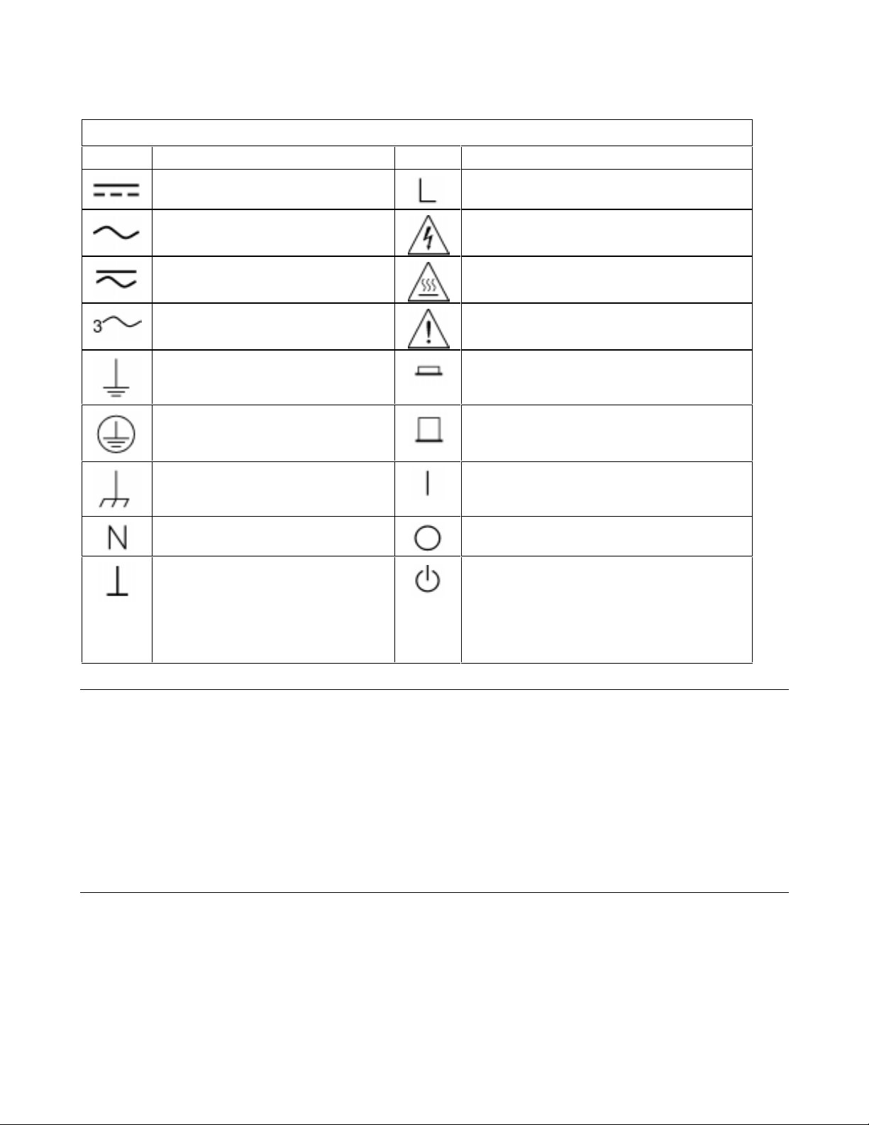
Safety Symbol Definitions
Symbol Description Symbol Description
Direct current Terminal for Line conductor on permanently
installed equipment
Alternating current Caution, risk of electric shock
Both direct and alternating current Caution, hot surface
Three-phase alternating current Caution (refer to accompanying documents)
Earth (ground) terminal In position of a bi-stable push control
Protective earth (ground) terminal
(Intended for connection to external
protective conductor.)
Frame or chassis terminal On (supply)
Terminal for Neutral conductor on
permanently installed equipment
Terminal is at earth potential
(Used for measurement and control
circuits designed to be operated with
one terminal at earth potential.)
Out position of a bi-stable push control
Off (supply)
Standby (supply)
Units with this symbol are not completely
disconnected from ac mains when this switch is
off. To completely disconnect the unit from ac
mains, either disconnect the power cord or have
a qualified electrician install an external switch.
Notice
The information contained in this document is subject to change without notice. Agilent Technologies makes no warranty of
any kind with regard to this material, including but not limited to, the implied wa rranties of merchantability, and fitness for a
particular purpose.
Agilent Technologies
connection with the furnishing, performance or use of this material.
This document contains proprietary information which is protected by copyright. All rights are reserved. No part of this
document may be photo copied, reproduced, or translated into another language without the prior written consent of Agilent
Technologies.
Copyright 1993, 2000 Agilent Technologies, Inc.
shall not be liable for errors contained herein or for incidental or consequential damages in
Printing History
The edition and current revision of this manual are indicated below. Repr ints of this manual containing minor corrections
and updates may have the same printing date. Revised editions are identified by a new printing date. A revised edition
incorporates all new or corrected material since the previous printing date.
First Edition ............July, 1993
Second Edition ...... September, 2000
4
Page 5

Table of Contents
Introduction............................................................................................................................................................................7
Scope .................................................................................................................................................................................. 7
Conventions Used In Text...................................................................................................................................................7
Manual Revisions................................................................................................................................................................8
Safety Considerations.........................................................................................................................................................8
Firmware Revisions ............................................................................................................................................................ 8
Electrostatic Discharge.......................................................................................................................................................8
Verification.............................................................................................................................................................................. 9
Introduction......................................................................................................................................................................... 9
Test Equipment Required....................................................................................................................................................9
Measurement Techniques..................................................................................................................................................11
Setup for Most Tests...................................................................................................................................................... 11
Electronic Load.............................................................................................................................................................. 11
Current-Monitoring Resistor.......................................................................................................................................... 11
Operation Verification Tests............................................................................................................................................. 11
Performance Tests.............................................................................................................................................................11
Programming..................................................................................................................................................................13
Constant Voltage (CV) Tests......................................................................................................................................... 13
CV Setup..................................................................................................................................................................... 13
Voltage Programming and Readback Accuracy.......................................................................................................... 13
CV Load Effect........................................................................................................................................................... 14
CV Source Effect........................................................................................................................................................14
CV Noise (PARD).......................................................................................................................................................14
Transient Recovery Time............................................................................................................................................ 15
Constant Current (CC) Tests.......................................................................................................................................... 15
CC Setup.....................................................................................................................................................................15
Current Programming and Readback Accuracy .......................................................................................................... 15
Current Sink (CC-) Operation.....................................................................................................................................16
CC Load and Line Regulation..................................................................................................................................... 16
CC Load Effect ........................................................................................................................................................... 16
CC Source Effect.........................................................................................................................................................17
CC Noise (PARD)....................................................................................................................................................... 17
Troubleshooting....................................................................................................................................................................31
Introduction....................................................................................................................................................................... 31
Test Equipment Required..................................................................................................................................................31
Overall Troubleshooting................................................................................................................................................... 34
Power-On Self-Test...........................................................................................................................................................34
Signature Analysis ............................................................................................................................................................ 35
Firmware Revisions (for Models 664xA & 665xA)....................................................................................................... 41
Test Headers .................................................................................................................................................................. 41
Troubleshooting Procedures.............................................................................................................................................49
Flow Charts....................................................................................................................................................................49
Bias and Reference Supplies.......................................................................................................................................... 49
CV/CC Status Annunciators Troubleshooting................................................................................................................ 49
Post Repair Calibration..................................................................................................................................................... 49
Inhibit Calibration Jumper.............................................................................................................................................49
Calibration Password.....................................................................................................................................................50
EEPROM Initialization.....................................................................................................................................................66
Transferring Calibration Constants Into Factory Preset Locations................................................................................... 66
5
Page 6

Disassembly Procedures...................................................................................................................................................72
List of Required Tools...................................................................................................................................................74
Top Cover, Removal & Replacement ............................................................................................................................ 74
A2 GPIB Board, Removal & Replacement (for 664xA & 665xA Models Only).......................................................... 74
A2 Isolator Board, Removal & Replacement (for 654xA & 655xA Only).................................................................... 75
Front Panel Assembly, Removal and Replacement........................................................................................................ 75
S1 Line Switch, Removal and Replacement...................................................................................................................76
A3 Front Panel Board, Removal and Replacement........................................................................................................ 76
A1 Main Board .............................................................................................................................................................. 77
A4 Heatsink Assembly (500 Watt Models 6x5xA Only)............................................................................................... 77
A4A1 or A4A3 Left Tunnel Board, Removal and Replacement.................................................................................... 78
A4A2 or A4A4 Right Tunnel Board..............................................................................................................................78
B1 Fan, Removal and Replacement...............................................................................................................................78
T1 Power Transformer, Removal and Replacement.......................................................................................................78
Principles of Operation........................................................................................................................................................81
Introduction....................................................................................................................................................................... 81
I/O INTERFACE SIGNALS.............................................................................................................................................81
Overall Block Diagram (Figure 4-2).................................................................................................................................83
Detailed Block Diagram Discussion.................................................................................................................................83
Secondary Interface Circuits (Figure 4-3)...................................................................................................................... 83
Output Power and Control Circuits (Figure 4-4)............................................................................................................ 86
Output Power .............................................................................................................................................................. 86
Control Circuits........................................................................................................................................................... 86
A3 Front Panel Board Circuits (Figure 4-5)................................................................................................................... 89
A2 GPIB Board Circuits For Agilent Models 664xA and 665xA Only......................................................................... 90
Isolator Board Circuits for Agilent Models 654xA and 665xA Only (Figure 4-7) ........................................................ 91
Replaceable Parts ................................................................................................................................................................. 95
Introduction....................................................................................................................................................................... 95
Chapter Organization..................................................................................................................................................... 95
Model Applicability....................................................................................................................................................... 95
How To Order Parts.......................................................................................................................................................... 95
Diagrams ............................................................................................................................................................................. 137
Introduction..................................................................................................................................................................... 137
Interconnections.............................................................................................................................................................. 137
AC Input and Transformer Connections......................................................................................................................... 137
Circuit Board Schematics................................................................................................................................................137
Component Location Diagrams ...................................................................................................................................... 137
Test Points ...................................................................................................................................................................... 139
Manual Backdating Changes............................................................................................................................................. 169
Index....................................................................................................................................................................................173
6
Page 7

Introduction
Scope
This manual contains information fo r troubleshooting and repairing four generic models of Agilent power supplies. The
different power supply models described in this manual are listed in Table 1-1.
Note The information provided in this manual applies to all Agilent models listed in Table 1-1. Where
differences exist among any of the models, these differences are explained in text.
For installation, operation, programming, and calibration procedures, refer to the appropriate Operating Manual as listed in
Chapter 2, Table 2-1. For information in determining the performance level of the power supply, either before or after
repair, refer to Chapter 2, Verification. The functional circuit operation of the various Agilent models is described in
Chapter 4. Replaceable parts lists and circuit diagrams are included in Chapters 5 and 6, respectively.
Table 1-1. Agilent Power Supplies Described In This Manual
Agilent Models 200 Watt Models 500 Watt Models
GPIB Agilent 6641A-6645A Agilent 6651A-6655A
Analog Programmable Agilent 6541A-6545A Agilent 6551A-6555A
1
Conventions Used In Text
1. Power supply models can be divided into 200 watt and 500 watt models. A "4" in the third position of the model
number indicates a 200 watt supply, while the digit "5" in the third position indicates a 500 watt unit.
2. In addition, power supplies can be divided according to GPIB supplies or Analog Programmable supplies. All GPIB
models have a “6” in the second position of the model number, while Analog Programmable supplies have a “5” in the
second position of the model number. The GPIB models include a GPIB bo a rd which permits communications between
the supply and an external computer over the GPIB bus. Analog Programmable supplies use an Isolator Board instead
of the GPIB board, and do not have the ability to communicate with an external computer.
3. When referring in text to either the 200 watt or 500 watt GPIB power supply models, the convention “models 664xA or
665xA,” respectively, is used. When referring to either the 200 watt or 500 watt non- GPIB (or Analog Programmable)
models, the convention “models 654xA or 655xA,” respectively, is used.
4. In this manual all complementary signal names in text are shown with an asterisk (*) after the signal name. Example;
PCLR*. In some schematic diagrams you may see a bar above the signal name, which is identical to the signal name
shown in text with an asterisk.
Introduction
7
Page 8

Manual Revisions
Agilent Technologies instruments are identified by a ten-character, serial number, such as, US36360101. This manual was
written for power supplies with serial numbers equal to, or higher than, those shown on the title page.
If the serial number on the rear panel of your power supply is higher than the one on the title page, then the power supply
was made after publication of this manual, and may have hardware and/or firmware differences not covered in this manual.
If there are such differences, they are documented in one or more yellow “Manual Changes” sheets sent with the manual.
If the serial number of your power supply is below that listed on the title page, or if it uses an older serial number format
such as 3023A-01456, then your power supply was made prior to those covered in this manual. If this is the case, refer to
Appendix A for any backdating information that may apply.
Safety Considerations
This product is a Safety Class 1 instrument that has a protective earth terminal. Refer to the Safety Summary page at the
beginning of this manual for general sa fety procedures and for the meaning of safety symbols appearing in the manual and
on the power supply.
Hazardous voltages exist within the power supply chassis, at the output terminals, and at the programming
terminals.
Firmware Revisions
The supply's firmware resides in the front panel board's ROM chip (A3U4), and in the main board's microprocessor chip
(AlU504). For models 664xA and 665xA, firmware also resides in the GPIB board ROM chip (A2U106).
For GPIB models 664xA and 665xA, you can use the “*IDN?” query, as described in Chapter 3, to get the firmware
revision numbers of your power supply's firmware. For Agilent models 654xA and 655xA, the revision number can be read
from the label affixed atop the IC chip.
Electrostatic Discharge
The power supply has components that can be damaged by ESD (electrostatic discharge). Failure to
observe standard antistatic practices can result in serious degradation of performance, even if complete
failure does not occur.
When working on the power supply, observe all standard antistatic work practices. This includes, but is not limited to:
■ Working at a static-free station, such as, a table covered with static-dissipative laminate or with an Agilent 9300-0797
conductive table mat.
■ Using a conductive wrist strap, such as, an Agilent 9300-0969 or an Agilent 9300-0970 wrist strap.
■ Grounding all metal equipment at the station to a single, common ground.
■ Connecting low-impedance test equipment to static-sensitive components only when those components have power
applied to them.
■ Removing power from the power supply before removing, or installing, printed circuit boards.
8
Introduction
Page 9

2
Verification
Introduction
This Chapter contains test procedures to verify that the Agilent Power Supply is operating normally. There are three types of
tests as follows:
Test Description
Built-In Self-Tests These tests are run automatically when the power supply is turned on.
Operation Verification These tests verify that the power supply is operating normally but the tests
do not check all specified operating parameters.
Performance Tests These tests check that the supply meets all of the operating specifications
as listed in the Operating Manual.
Note The power supply must pass the built-in self-tests before the tests in this chapter can be performed. If the
supply fails the self test, refer to the overall troubleshooting procedures in Chapter 3 of this manual.
If any failures are encountered, or if abnormal test results are observed, refer to the Troubleshooting Procedures in Chapter
3 of this manual. The troubleshooting procedures will determine if repair and/or calibration is required. Calibration
procedures are given in Appendix A of the appropriate Operating Manual.
Table 2-1. Applicable Agilent Power Supply Operating Manuals
For Agilent Model Operating Manual Part Number
GPIB Models 664xA & 665xA 5964-8267
Analog Programmable Models 654xA & 655xA 5959-3374
Test Equipment Required
Table 2-2 lists the equipment required to perform the verification tests.
SHOCK HAZARD. The test should only be performed by qualified personnel. During the performance of
these tests, hazardous voltages may be present at the output of the supply.
Verification 9
Page 10

Table 2-2. Test Equipment Required for Verification
Type Required Characteristics Recommended Model
Current Monitor Resistor
DC Power Supply
Digital Voltmeter
Electronic Load
GPIB Controller
1
Load Resistor
100 A (0.01 Ω) ±0.04% for Agilent
Guildline 9230/100
6541A, 6551A, 6552A, 6641A,
6651A, & 6652A models.
15 A (0.1 Ω) ±0.04% for
Agilent
Guildline 9230/15
6542A, 6543A, 6544A, 6545A,
6553A, 6554A, 6555A, 6642A,
6643A, 6644A, 6645A, 6653A,
6654A, 6655A models.
5 V @ 10 A Agilent 66 Agilent 42A, 6653A
Resolution: 10 nV @ 1 V Agilent 3458A
Readout: 8 1/2 digits
Accuracy: 20 ppm
Voltage and curre nt range must
exceed range of supply under test.
Power range: 250 W minimum
Agilent
A
m
N3300A mainframe with
N3306A (60 V) plug-in
gilent
odule or Agilent
N3305A (150 V)
plug-in module.
Full GPIB capabilities Agilent 82350B
0.1 Ω ±5%, 300 W for Agilent
Ohmite C300KRlO
6541A, 6641A, 6551A, 6651A,
6552A, 6652A models.
Oscilloscope
RMS Voltmeter
Variable-Voltage Transformer
1
For 664xA and 665xA models only.
l.0 Ω ±5%, 300 W for Agilent
Ohmite C300KlRO
6542A, 6543A, 6544A, 6545A,
6553A, 6554A, 6555A, 6642A,
6643A, 6644A, 6645A, 6653A,
6654A, 6655A models.
Sensitivity: 1 mV Agilent
Infiniium
Bandwidth Limit: 20 MHz
Probe: 1:1 with RF tip
True RMS Bandwidth: 20 MHz Agilent 3400B
Sensitivity: 100 µV
Adjustable from -13% to +6% of
input range. Power: 1 kV A
minimum.
10 Verification
Page 11

Measurement Techniques
Setup for Most Tests
Most tests are performed at the rear terminals of the supply as shown in Figure 2-1. Measure the DC voltage directly at the
+S and -S terminals. Set the output for remote sensing and use adequate wire gauge for the load leads as described in
Chapter 4 of the Operating Manual.
Note All tests are performed as follows: Set the SENSE switch at the back of the supply to the Remote position.
Connect the remote sensing leads from +OUT to +S, and from -OUT to -S.
Electronic Load
Many of the test procedures require the use of a variable load capable of dissipating the required power. If a variable
resistor is used, switches must be used to either; connect, disconnect, or short the load resistor. For most tests, an electronic
load can be used. The electronic load is considerably easier to use than load resistors, but it may not be fast enough to test
transient recovery time and may be too noisy for the noise (PARD) tests.
Fixed load resistors may be used in place of a variable load, with minor changes to the test procedures in this chapter. Also,
if computer controlled test setups are used, the relatively slow (compared to computers and system voltmeters) settling times
and slew rates of the power supply may have to be taken into account. "Wait" statements can be used in the test program if
the test system is faster than the supply.
Current-Monitoring Resistor
To eliminate output-current measurement error caused by voltage drops in the leads and connections, connect the current
monitoring resistor between the -OUT and the load as a four terminal device. Connect the current-monitoring leads inside
the load-lead connections directly at the monitoring points on the resistor element.
Operation Verification Tests
To assure that the supply is operating prope rly, without testing all specified parameters, perform the following test
procedures:
a. Perform the turn-on and checkout procedures given in Chapter 3 of the Operating Manual.
b. Perform the Voltage Programming and Readback Accuracy test, and the Current Programming and Readback Accuracy
Performance test which are given in this chapter.
Performance Tests
Note A full Performance Test consists of those items listed as Specifications in Table 1-1 of the Operating
Manual, that have a procedure in the Verification section of this chapter.
The following paragraphs provide test procedures for verifying the supply’s compliance with the specifications listed in
Table 1-1 of the Operating Manual. All of the performance test specifications are listed in the appropriate Performance Te st
Record Form for your specific model. You can record the actual measured values in the column provided in this form.
Verification 11
Page 12
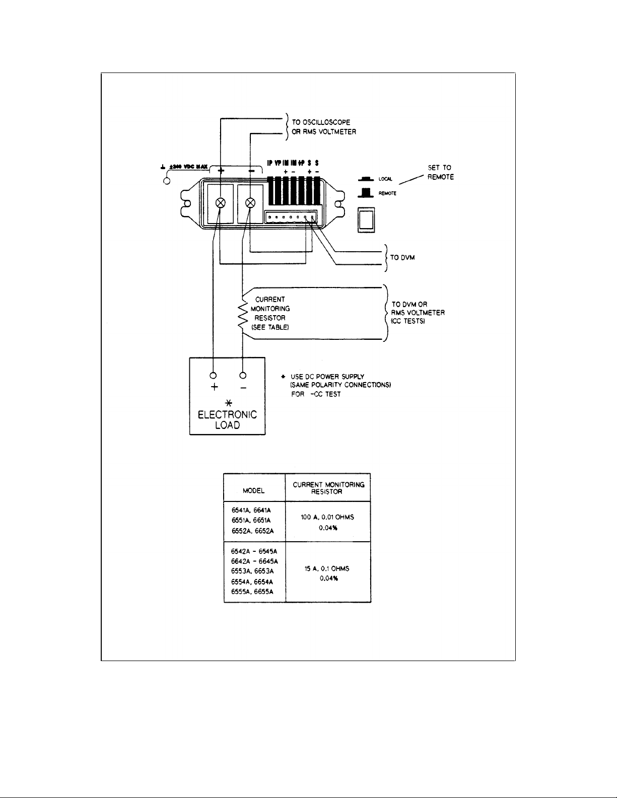
(
CV TESTS
)
(CV TESTS)
Figure 2-1. Basic Test Setup
12 Verification
Page 13

Programming
You can program the supply from the front panel keyboard or from a GPIB controller (for models 664xA and 665xA) when
performing the tests. The test procedures are written assuming that you know how to program the supply either; remotely
from a GPIB controller (for 664xA and 665xA models), or locally using the control keys and indicators on the supply’s front
panel. For models 654xA and 655xA you must use the front panel. Complete instructions on remote and local programming
are given in the Opera ting Manual.
Constant Voltage (CV) Tests
CV Setup
If more than one meter or if a meter and an oscilloscope are used, connect each to the terminals by a separate pair of leads to
avoid mutual coupling effects. For constant voltage DC tests, connect only to +S and -S, since the unit regulates the output
voltage that appears between +S and -S, and not between the (+) and (-) output terminals. Use coaxial cable or shielded
two-wire cable to avoid noise pickup on the test leads.
Voltage Programming and Readback Accuracy
This test verifies that the voltage programming, GPIB readback (on 664xA and 665xA models), and front panel display
functions are within specifications. Note that the values read back over the GPIB should be identical to those displayed on
the front panel.
a. Turn off the supply and connect a digital voltmeter between the +S and the -S terminals as shown in Figure 2-1.
b. Turn on the supply and program the supply to zero volts and the maximum programmable current (see Table 2-3) with
the load off.
c. Record the output voltage readings on the digital voltmeter (DVM) and the front panel display. The readings should be
within the limits specified in the performance test record form for the appropriate model under CV PROGRAMMING
@ 0 VOLTS. Also, note that the CV annunciator is on. The output current reading should b e approximately zero.
d. Program the output voltage to full-scale (see Table 2-3).
e. Record the output voltage readings on the DVM and the front panel display. The readings should be within the limits
specified in the performance test record form for the appropriate model under CV PROGRAMMING @ FULL
SCALE.
Table 2-3. Voltage and Current Values
Agilent Model Full-Scale
Voltage
6541A, 6641A 8 V 8.190 V 20 A 20.475 A 8.8 V
6542A, 6642A 20 V 20.475 V 10 A 10.237 A 22 V
6543A, 6643A 35 V 35.831 V 6 A 6.142 A 38.5 V
6544A, 6644A 60 V 61.425 V 3.5 A 3.583 A 66.0 V
6545A, 6645A 120 V 122.85 V 1.5 A 1.535 A 132 V
6551A, 6651A 8 V 8.190 V 50 A 51.188 A 8.8 V
6552A, 6652A 20 V 20.475 V 25 A 25.594 A 22 V
6553A, 6653A 35 V 35.831 V 15 A 15.536 A 38.5 V
6554A, 6654A 60 V 61.425 V 9 A 9.214 A 66.0 V
6555A, 6655A 120 V 122.85 V 4 A 4.095 A 132 V
Max. Prog.
Voltage
200 Watt Supplies
500 Watt Supplies
Full-Scale
Current
Max. Prog.
Current
Max. Prog.
Overvoltage
Verification 13
Page 14

CV Load Effect
This test measures the change in output voltage resulting from a change in output current from full load to no load.
a. Turn off the supply and connect the output as shown in Figure 2-1 with the DVM connected between the +S and -S
terminals.
b. Turn on the supply and program the current to the maximum programmable value and the voltage to the full-scale value
(see Table 2-3).
c. Adjust the load for the full-sc ale current (see Table 2-3) as indicated on the front panel display. The CV annunciator o n
the front panel must be on. If it is not, adjust the load so that the output current drops slightly.
d. Record the output voltage reading on the DVM connected to +S and -S.
e. Open the load and again record the DVM voltage reading.
The difference between the DVM readings in steps (d) and (e) is the load effect voltage, and should not exceed the value
listed in the Performance Test Record Form for the appropriate model under CV LOAD EFFECT.
CV Source Effect
This test measures the change in output voltage that results from a change in AC line voltage from the minimum to
maximum value within the line voltage specifications.
a. Turn off the supply and connect the AC power line through a variable voltage transformer.
b. Connect the output as shown in Figure 2-1 with the DVM connected between the +S and the -S terminals. Set the
transformer to nominal line voltage.
c. Turn on the supply and program the current to the maximum programmable value and the output voltage to the
full-scale value (see Table 2-3).
d. Adjust the load for the full-scale current value (see Table 2-3) as indicated on the front panel display. The CV
annunciator on the front pa nel must be on. If it is not, adjust the load so that the output current drops slightly.
e. Adjust the transformer to 13% below the nominal line voltage (e.g., l04.4 Vac for a 120 Vac nominal line voltage
input).
f. Record the output voltage reading on the DVM.
g. Adjust the transformer to 6% above the nominal line voltage (e.g., 127.2 Vac for 120 Vac nominal line voltage input).
h. Record the output voltage reading on the DVM.
The difference between the DVM reading in steps (f) and (h) is the source effect voltage and should not exceed the value
listed in the Performance Test Record Form for the appropriate model under CV SOURCE EFFECT .
CV Noise (PARD)
Periodic and random deviations (PARD) in the output (ripple and noise) combine to produce a residual AC voltage
superimposed on the DC output voltage. CV PARD is specified as the rms or peak-to-peak output voltage in a frequency
range from 20 Hz to 20 MHz.
a. Turn off the supply and connect the output as shown in Figure 2-1 to an oscilloscope (AC coupled) between the (+) and
the (-) terminals. Set the oscilloscope’s bandwidth limit to 20 MHz and use an RF tip on the oscilloscope probe.
b. Turn on the supply and program the current to the maximum programmable value and the output voltage to the
full-scale value (see Table 2-3).
c. Adjust the load for the full-scale current value (see Table 2-3) as indicated on the front panel display.
d. Note that the waveform on the oscilloscope should not exceed the peak-to-peak limits in the Performance Test Record
Form for the appropriate model under CV NOISE (PARD).
e. Disco nnect the oscilloscope and connect an AC rms voltmeter in its place. The rms voltage reading should not exceed
the RMS limits in the Performance Test Record Form for the appropriate model under CV NOISE (PARD).
14 Verification
Page 15

Transient Recovery Time
This test measures the time for the output voltage to recover to within the specified value following a 50% change in the
load current.
a. Turn off the supply and connect the output as in Figure 2-1 with the oscilloscope across the +S and the -S terminals.
b. Turn on the supply and program the output voltage to the full-scale value and the current to the maximum
programmable value (see Table 2-3).
c. Set the load to the Constant Current mode and program the load current to 1/2 the power supply full-scale rated current.
d. Set the electronic load’s transient generator frequency to l00 Hz and its duty cycle to 50%.
e. Program the load’s transient current level to the supply’s full-scale current value and turn the transient on.
f. Adjust the oscilloscope for a waveform similar to that in Figure 2-2.
g. The output voltage should return to within 0.1% o r 20 mV, whichever is greater, of the nominal value in less than 100
microseconds. Check both loading and unload ing transients by triggering on the positive and negative slope.
Figure 2-2. Transient Response Wavetorm
Constant Current (CC) Tests
CC Setup
Follow the general setup instructions in the Measurement Techniques paragraph and the specific instructions given in the
following paragrap hs.
Current Programming and Readback Accuracy
This test verifies that the current programming and readback are within specification. The accuracy of the current
monitoring resistor must be 0.04% or better.
a. Turn off the supply and connect the current monitoring resistor across the output and a DVM across the resistor. See
Current Monitoring Resistor.
b. Turn on the supply and program the output voltage to 5 V and the current to zero.
c. Divide the voltage drop (DVM reading) across the current monitoring resistor by its resistance to convert to amps and
record this value (Iout). Also, record the current reading on the front panel display. The readings should be within the
limits specified in the Performance Test Record Form for the appropriate model under CC PRGRAMMING @ 0 AMPS.
d. Program the output voltage to 5 V and the current to full-scale (see Table 2-3).
Verification 15
Page 16
e. Divide the voltage drop (DVM reading) across the current monitoring resistor by its resistance to convert to amps and
record this value (Iout). Also, record the current reading that appears on the front panel display. The readings should be
within the limits specified in the performance test record form for the appropriate model under CC PROGRAMMING
@ FULL-SCALE.
Current Sink (CC-) Operation.
This test verifies current sink operation and readback.
a. Turn off the supply and connect the output as shown in Figure 2-1, except connect a DC power supply in place of the
electronic load as indicated.
b. Set the external power supply to 5 V and its current limit to 20% of the full scale current value (see Table 2-3) of the
supply under test. For example, if the full scale current value is 25 A, set the external supply’s current limit to 5 A.
c. Turn on the supply under test and program the output voltage to zero. The current on the UUT display should be
approximately 20% of the full-scale current.
d. Divide the voltage drop across the current monitoring resistor by its resistance to obtain the current sink value in amps
and subtract this from the current reading on the display. The difference between the readings should be within the
limits specified in the Performance Test Record Form for the appropriate model under, CURRENT SINK DISPLAY
AND READBACK.
CC Load and Line Regulation
These tests (CC Load Effect and CC Source Effect given below) are tests of the DC regulation of the power supply’s output
current. To insure that the values read are not the instantaneous measurement of the AC peaks of the output current ripple,
several DC measurements should be made and the average of these reading calculated. An example of how to do this is
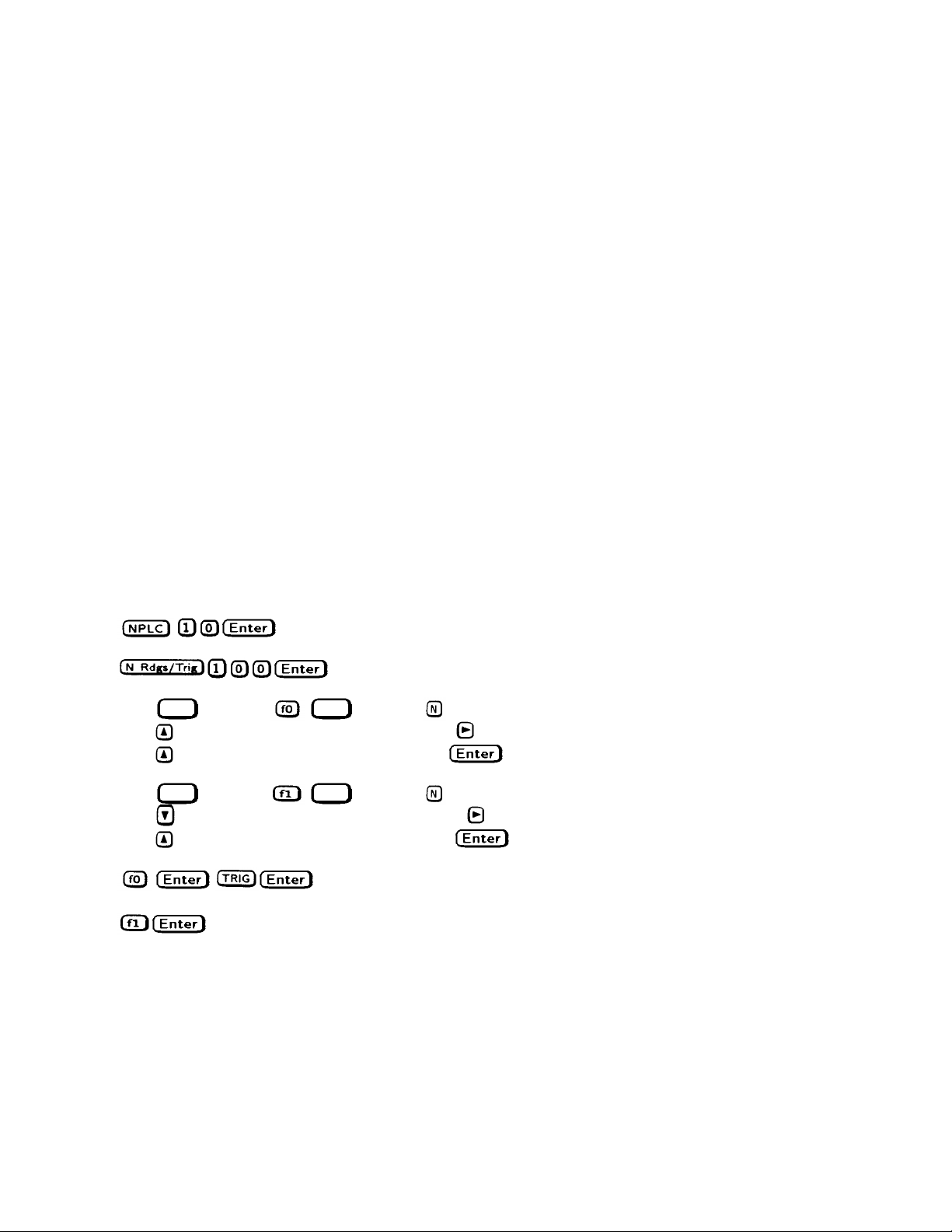
given below using an Agilent 3458A System Voltmeter programmed from the front panel. Set up the voltmeter and execute
the “Average Reading” program as follows:
a. Program 10 power line cycles per sample by pressing
b. Program 100 samples per trigger by pressing
c. Set up voltmeter to take measurements in the statistical mode as follows:
Press
Press
Press
d. Set up voltmeter to read the average of the measurements as follows:
Press
Press
Press
e. Execute the program by pressing
f. Wait for 100 readings and then read the average measurement by pressing
To repeat the measurement, perform steps (e) and (f).
CC Load Effect
This test measures the change in output current for a change in the load from full scale output voltage to short circuit.
.
.
(shift key)
until MATH function is selected, then press .
until STAT function is selected, then press .
(shift key)
until RMATH function is selected, then press .
until MEAN function is selected, then press .
.
.
(shift key)
(shift key)
.
.
a. Turn off the supply and connect the output as shown in Figure 2-1 with the DVM connected across the current
monitoring resistor.
16 Verification
Page 17

b. Turn on the supply and program the current to the full scale current value and the output voltage to the maximum
programmable voltage value (see Table 2-3).
c. Adjust the load in the CV mode for full scale voltage as indicated on the front panel display. Check that the CC
annunciator is on. If it is not, adjust the load so that the outp ut voltage drops slightly.
d. *Record the output current reading (DVM reading/current monitor resistance value in ohms).
e. *Short the load switch and record the output current reading.
The difference in the current readings in steps (d) and (e) is the load effect and should not exceed the limit specified in the
Performance Test Record Form for the appropriate model under CC LOAD EFFECT.
* You may want to use the average reading program described previously.
CC Source Effect
This test measures the change in output current that results when the AC line voltage changes from the minimum to the
maximum value within the specifications.
a. Turn off the supply and connect the AC power line through a variable voltage transformer.
b. Connect the output terminals as shown in Figure 2-1 with the DVM connected across the current monitoring resistor.
Set the transformer to the nominal line voltage.
c. Turn on the supply and program the current to the full scale value and the output voltage to the maximum
programmable value (see Table 2-3).
d. Adjust the load in the CV mode for full scale voltage as indicated on the front panel display. Check that the CC
annunciator is on. If it is not, adjust the load so that the outp ut voltage drops slightly.
e. Adjust the transformer to 13% below the nominal line voltage.
f. *Record the output current reading (DVM reading/current monitoring resistor in ohms).
g. Adjust the transformer to 6% above the nominal line voltage.
h. *Record the output current reading again.
The difference in the current readings in steps (f) and (h) is the CC source effect and should not exceed the values listed in
the Performance Test Record Form for the appropriate model under CC SOURCE EFFECT.
*You may want to use the average reading program described previously.
CC Noise (PARD)
Periodic and random deviations (PARD) in the output (ripple and noise) combine to produce a residual AC current, as well,
as an AC voltage superimposed on the DC output. Constant current (CC) PARD is specified as the rms output current in a
frequency range 20 Hz to 20 MHz with the supply in CC operation.
a. Turn off the supply and connect the load resistor and rms voltmeter as shown in Figure 2-3. Leads should be as short as
possible to reduce noise pick-up. Use only a resistive load for this test.
b. Check the test setup for noise with the supply turned off. Other equipment (e.g. computer, DMM, etc.) may affect the
reading.
c. Turn on the supply and program the current to full scale and the output voltage to the maximum programmable value
(see Table 2-3).
d. The output current should be at the full scale rating with the CC annunciator on.
e. Divide the reading on the rms voltmeter by the load resistance to obtain rms current. It should not exceed the values
listed in the Performance Test Record Form for the appropriate model under CC NOISE (RMS).
Verification 17
Page 18

18 Verification
Figure 2-3. CC RMS Noise Measurement Test Setup
Page 19

Table 2-4. Performance Test Record Form
Test Facility:
__________________________________________ Report No.__________________________________________
__________________________________________ Date______________________________________________
__________________________________________ Customer___________________________________________
__________________________________________ Tested By___________________________________________
Model_____________________________________ Ambient Temperature__________________________________
Serial No.__________________________________ Relative Humidity_____________________________________
Options ___________________________________ Nominal Line Frequency (Hz)___________________________
Firmware Revision___________________________
Special Notes:
____________________________________________________________________________________________
____________________________________________________________________________________________
____________________________________________________________________________________________
____________________________________________________________________________________________
____________________________________________________________________________________________
____________________________________________________________________________________________
____________________________________________________________________________________________
____________________________________________________________________________________________
____________________________________________________________________________________________
Test Equipment Used:
Description Model No. Trace No. Cal. Due Date
1. AC Source ________ ___________ ___________
2. DC Voltmeter ________ ___________ ___________
3. RMS Voltmeter ________ ___________ ___________
4. Oscilloscope ________ ___________ ___________
5. Electronic Load ________ ___________ ___________
6. Current Monitoring ________ ___________ ___________
Shunt
Verification 19
Page 20
Table 2-5. Performance Test Record for Agilent Model 6541A or 6641A
MODEL Agilent _____________
Test Description
Voltage Programming
and Readback
Report No.______________ Date_____________________
Minimum
Spec.
Results
*
Maximum
Spec.
Constant Voltage Tests
Low Voltage (0 V) V
out
Front Panel Display Readback
High Voltage (8 V) V
out
Front Panel Display Readback
Load Effect
Source Effect
PARD (Ripple and Noise)
Peak-to-Peak
RMS
Transient Response Time
(at 100 µs)
Current Programming
and Readback
Low Current (0 A) I
out
Front Panel Display Readback
-5 mV
- 6 mV
V
out
7.9902 V
- 11.6 mV
V
out
V
- 1 mV _______mV V
out
V
- 0.5 mV _______mV V
out
0
0
________mV
________mV
_________V
_______mV
_______mV
_______µV
0 _______mV 20 mV
Constant Current Tests
-26 mA
- 18 mA
I
out
_______mA
_______mA
+5 mV
V
+ 6 mV
out
8.0098 V
V
+ 11.6 mV
out
+ 1 mV
out
+ 0.5 mV
out
3 mV
300 µV
+26 mA
I
+ 18 mA
out
High Current (20 A) I
out
Front Panel Display Readback
Current Sink (4 A) Display Readback
PARD (Ripple and Noise)
RMS
Load Effect
Source Effect
20 Verification
+19.944 A
- 48 mA
I
out
I
- 54 mA _______mA I
sink
_________A
_______mA
0 ________mA 10 mA
I
- 1 mA ________mA I
out
I
- 1 mA ________mA I
out
*Enter your test results in this column.
+20.056 A
I
+ 48 mA
out
+ 54 mA
sink
+ 1 mA
out
+ 1 mA
out
Page 21

Table 2-6. Performance Test Record for Agilent Model 6542A or 6642A
MODEL Agilent _____________
Test Description
Voltage Programming
and Readback
Report No.______________ Date_____________________
Minimum
Spec.
Results
*
Maximum
Spec.
Constant Voltage Tests
Low Voltage (0 V) V
out
Front Panel Display Readback
High Voltage (20 V) V
out
Front Panel Display Readback
Load Effect
Source Effect
PARD (Ripple and Noise)
Peak-to-Peak
RMS
Transient Response Time
(at 100 µs)
Current Programming
and Readback
Low Current (0 A) I
out
Front Panel Display Readback
-10 mV
- 15 mV
V
out
19.978 V
- 29 mV
V
out
V
- 2 mV _______mV V
out
V
- 0.5 mV _______mV V
out
0
0
________mV
________mV
_________V
_______mV
_______mV
_______µV
0 _______mV 20 mV
Constant Current Tests
-13 mA
- 9.1 mA
I
out
_______mA
_______mA
+10 mV
V
+ 15 mV
out
20.022 V
V
+ 29 mV
out
+ 2 mV
out
+ 0.5 mV
out
3 mV
300 µV
+13 mA
I
+ 9.1 mA
out
High Current (10 A) I
out
Front Panel Display Readback
Current Sink (2 A) Display Readback
PARD (Ripple and Noise)
RMS
Load Effect
Source Effect
+ 9.972 A
- 24.1 mA
I
out
I
- 27 mA _______mA I
sink
_________A
_______mA
0 ________mA 5 mA
I
- 0.5 mA ________mA I
out
I
- 0.5 mA ________mA I
out
*Enter your test results in this column.
+10.028 A
I
+ 24.1 mA
out
+ 27 mA
sink
+ 0.5 mA
out
+ 0.5 mA
out
Verification 21
Page 22

Table 2-7. Performance Test Record for Agilent Model 6543A or 6643A
MODEL Agilent _____________
Test Description
Voltage Programming
and Readback
Report No.______________ Date_____________________
Minimum
Spec.
Results
*
Maximum
Spec.
Constant Voltage Tests
Low Voltage (0 V) V
out
Front Panel Display Readback
High Voltage (35 V) V
out
Front Panel Display Readback
Load Effect
Source Effect
PARD (Ripple and Noise)
Peak-to-Peak
RMS
Transient Response Time
(at 100 µs)
Current Programming
and Readback
Low Current (0 A) I
out
Front Panel Display Readback
-15 mV
- 25 mV
V
out
34.964 V
- 49.5 mV
V
out
V
- 3 mV _______mV V
out
V
- 1 mV _______mV V
out
0
0
________mV
________mV
_________V
_______mV
_______mV
_______µV
0 _______mV 35 mV
Constant Current Tests
-6.7 mA
- 5 mA
I
out
_______mA
_______mA
+15 mV
V
+ 25 mV
out
35.036 V
V
+ 49.5 mV
out
+ 3 mV
out
+1 mV
out
4 mV
400 µV
+6.7 mA
I
+ 5 mA
out
High Current (6 A) I
out
Front Panel Display Readback
Current Sink (1.2 A) Display Readback
PARD (Ripple and Noise)
RMS
Load Effect
Source Effect
22 Verification
+5.9843 A
- 14 mA
I
out
I
-16.2 mA _______mA I
sink
_________A
_______mA
0 ________mA 3 mA
I
- 0.25 mA ________mA I
out
I
- 0.25 mA ________mA I
out
*Enter your test results in this column.
+6.0157 A
I
+ 14 mA
out
+16.2 mA
sink
+ 0.25 mA
out
+ 0.25 mA
out
Page 23

Table 2-8. Performance Test Record for Agilent Model 6544A or 6644A
MODEL Agilent _____________
Test Description
Voltage Programming
and Readback
Report No.______________ Date_____________________
Minimum
Spec.
Results
*
Maximum
Spec.
Constant Voltage Tests
Low Voltage (0 V) V
out
Front Panel Display Readback
High Voltage (60 V) V
out
Front Panel Display Readback
Load Effect
Source Effect
PARD (Ripple and Noise)
Peak-to-Peak
RMS
Transient Response Time
(at 100 µs)
Current Programming
and Readback
Low Current (0 A) I
out
Front Panel Display Readback
-26 mV
- 40 mV
V
out
59.938 V
- 82 mV
V
out
V
- 4 mV _______mV V
out
V
- 1 mV _______mV V
out
0
0
________mV
________mV
_________V
_______mV
_______mV
_______µV
0 _______mV 60 mV
Constant Current Tests
-4.1 mA
- 3 mA
I
out
_______mA
_______mA
+26 mV
V
+ 40 mV
out
60.062 V
V
+ 82 mV
out
+ 4 mV
out
+ 1 mV
out
5 mV
500 µV
+4.1 mA
I
+ 3 mA
out
High Current (3.5 A) I
out
Front Panel Display Readback
Current Sink (0.7 A) Display Readback
PARD (Ripple and Noise)
RMS
Load Effect
Source Effect
+3.49065 A
- 8.25 mA
I
out
I
- 9.25 mA _______mA I
sink
_________A
_______mA
0 ________mA 1.5 mA
I
- 0.25 mA ________mA I
out
I
- 0.25 mA ________mA I
out
*Enter your test results in this column.
+3.50935 A
I
+ 8.25 mA
out
+ 9.25 mA
sink
+ 0.25 mA
out
+ 0.25 mA
out
Verification 23
Page 24

Table 2-9. Performance Test Record for Agilent Model 6545A or 6645A
MODEL Agilent _____________
Test Description
Voltage Programming
and Readback
Report No.______________ Date_____________________
Minimum
Spec.
Results
*
Maximum
Spec.
Constant Voltage Tests
Low Voltage (0 V) V
out
Front Panel Display Readback
High Voltage (120 V) V
out
Front Panel Display Readback
Load Effect
Source Effect
PARD (Ripple and Noise)
Peak-to-Peak
RMS
Transient Response Time
(at 100 µs)
Current Programming
and Readback
Low Current (0 A) I
out
Front Panel Display Readback
-51 mV
- 80 mV
V
out
119.877 V
- 164 mV
V
out
V
- 5 mV _______mV V
out
V
- 2 mV _______mV V
out
0
0
________mV
________mV
_________V
_______mV
_______mV
_______µV
0 _______mV 120 mV
Constant Current Tests
-1.7 mA
- 1.3 mA
I
out
_______mA
_______mA
+51 mV
V
+ 80 mV
out
120.123 V
V
+ 164 mV
out
+ 5 mV
out
+ 2 mV
out
7 mV
700 µV
+1.7 mA
I
+ 1.3 mA
out
High Current (1.5 A) I
out
Front Panel Display Readback
Current Sink (0.3 A) Display Readback
PARD (Ripple and Noise)
RMS
Load Effect
Source Effect
24 Verification
+1.49605 A
- 3.55 mA
I
out
- 3.95 mA _______mA I
I
sink
_________A
_______mA
0 ________mA 1 mA
I
- 0.25 mA ________mA I
out
I
- 0.25 mA ________mA I
out
*Enter your test results in this column.
+1.50395 A
I
+ 3.55 mA
out
+ 3.95 mA
sink
+ 0.25 mA
out
+ 0.25 mA
out
Page 25

Table 2-10. Performance Test Record for Agilent Model 6551A or 6651A
MODEL Agilent _____________
Test Description
Voltage Programming
and Readback
Report No.______________ Date_____________________
Minimum
Spec.
Results
*
Maximum
Spec.
Constant Voltage Tests
Low Voltage (0 V) V
out
Front Panel Display Readback
High Voltage (8 V) V
out
Front Panel Display Readback
Load Effect
Source Effect
PARD (Ripple and Noise)
Peak-to-Peak
RMS
Transient Response Time
(at 100 µs)
Current Programming
and Readback
Low Current (0 A) I
out
Front Panel Display Readback
-5 mV
- 6 mV
V
out
7.990
2 V
- 11.6 mV
V
out
V
- 1 mV _______mV V
out
V
- 0.5 mV _______mV V
out
0
0
________mV
________mV
_________V
_______mV
_______mV
_______µV
0 _______mV 20 mV
Constant Current Tests
-
60 mA
- 67 mA
I
out
_______mA
_______mA
+5 mV
V
+ 6 mV
out
8.0098 V
V
+ 11.6 mV
out
+ 1 mV
out
+ 0.5 mV
out
3 mV
300 µV
+60 mA
I
+ 67 mA
out
High Current (50 A) I
out
Front Panel Display Readback
Current Sink (10 A) Display Readback
PARD (Ripple and Noise)
RMS
Load Effect
Source Effect
+49.865 A
- 142 mA
I
out
I
-135 mA ________mA I
sink
_________A
_______mA
0 ________mA 25 mA
I
- 2 mA ________mA I
out
I
- 2 mA ________mA I
out
*Enter your test results in this column.
+50.135 A
I
+ 142 mA
out
+135 mA
sink
+ 2 mA
out
+ 2 mA
out
Verification 25
Page 26

Table 2-11. Performance Test Record for Agilent Model 6552A or 6652A
MODEL Agilent _____________
Test Description
Voltage Programming
and Readback
Report No.______________ Date_____________________
Minimum
Spec.
Results
*
Maximum
Spec.
Constant Voltage Tests
Low Voltage (0 V) V
out
Front Panel Display Readback
High Voltage (20 V) V
out
Front Panel Display Readback
Load Effect
Source Effect
PARD (Ripple and Noise)
Peak-to-Peak
RMS
Transient Response Time
(at 100 µs)
Current Programming
and Readback
Low Current (0 A) I
out
Front Panel Display Readback
-10 mV
- 15 mV
V
out
19.978 V
- 29 mV
V
out
V
- 2 mV _______mV V
out
V
- 0.5 mV _______mV V
out
0
0
________mV
________mV
_________V
_______mV
_______mV
_______µV
0 _______mV 20 mV
Constant Current Tests
-25 mA
- 26 mA
I
out
_______mA
_______mA
+10 mV
V
+ 15 mV
out
20.022 V
V
+ 29 mV
out
+ 2 mV
out
+ 0.5 mV
out
3 mV
300 µV
+25 mA
I
+ 26 mA
out
High Current (25 A) I
out
Front Panel Display Readback
Current Sink (5 A) Display Readback
PARD (Ripple and Noise)
RMS
Load Effect
Source Effect
26 Verification
+24.9375 A
- 63.5 mA
I
out
I
-61.5 mA _______mA I
sink
_________A
_______mA
0 ________mA 10 mA
I
- 1 mA ________mA I
out
I
- 1 mA ________mA I
out
*Enter your test results in this column.
+25.0625 A
I
+ 63.5 mA
out
+61.5 mA
sink
+ 1 mA
out
+ 1 mA
out
Page 27

Table 2-12. Performance Test Record for Agilent Model 6553A or 6653A
MODEL Agilent _____________
Test Description
Voltage Programming
and Readback
Report No.______________ Date_____________________
Minimum
Spec.
Results
*
Maximum
Spec.
Constant Voltage Tests
Low Voltage (0 V) V
out
Front Panel Display Readback
High Voltage (35 V) V
out
Front Panel Display Readback
Load Effect
Source Effect
PARD (Ripple and Noise)
Peak-to-Peak
RMS
Transient Response Time
(at 100 µs)
Current Programming
and Readback
Low Current (0 A) I
out
Front Panel Display Readback
-15 mV
- 25 mV
V
out
34.964 V
- 49.5 mV
V
out
V
- 3 mV _______mV V
out
V
- 1 mV _______mV V
out
0
0
________mV
________mV
_________V
_______mV
_______mV
_______µV
0 _______mV 35 mV
Constant Current Tests
-13 mA
- 15 mA
I
out
_______mA
_______mA
+15 mV
V
+ 25 mV
out
35.036 V
V
+ 49.5 mV
out
+ 3 mV
out
+1 mV
out
4 mV
400 µV
+13 mA
I
+ 15 mA
out
High Current (15 A) I
out
Front Panel Display Readback
Current Sink (3 A) Display Readback
PARD (Ripple and Noise)
RMS
Load Effect
Source Effect
+14.9645 A
- 37.5 mA
I
out
I
-34.5 mA _______mA I
sink
_________A
_______mA
0 ________mA 5 mA
I
-0.5 mA ________mA I
out
I
- 0.75 mA ________mA I
out
*Enter your test results in this column.
+15.0355 A
I
+ 37.5 mA
out
+34.5 mA
sink
+ 0.5 mA
out
+ 0.75 mA
out
Verification 27
Page 28

Table 2-13. Performance Test Record for Agilent Model 6554A or 6654A
MODEL Agilent _____________
Test Description
Voltage Programming
and Readback
Report No.______________ Date_____________________
Minimum
Spec.
Results
*
Maximum
Spec.
Constant Voltage Tests
Low Voltage (0 V) V
out
Front Panel Display Readback
High Voltage (60 V) V
out
Front Panel Display Readback
Load Effect
Source Effect
PARD (Ripple and Noise)
Peak-to-Peak
RMS
Transient Response Time
(at 100 µs)
Current Programming
and Readback
Low Current (0 A) I
out
Front Panel Display Readback
-26 mV
- 40 mV
V
out
59.938 V
- 82 mV
V
out
V
- 4 mV _______mV V
out
V
- 1 mV _______mV V
out
0
0
________mV
________mV
_________V
_______mV
_______mV
_______µV
0 _______mV 60 mV
Constant Current Tests
-8 mA
I
out
- 7 mA
_______mA
_______mA
+26 mV
V
+ 40 mV
out
60.062 V
V
+ 82 mV
out
+ 4 mV
out
+ 1 mV
out
5 mV
500 µV
+8 mA
I
+ 7 mA
out
High Current (9 A) I
out
Front Panel Display Readback
Current Sink (1.8 A) Display Readback
PARD (Ripple and Noise)
RMS
Load Effect
Source Effect
28 Verification
+8.9785 A
- 20.5 mA
I
out
I
-21.3 mA _______mA I
sink
_________A
_______mA
0 ________mA 3 mA
I
- 0.5 mA ________mA I
out
I
-0.5 mA ________mA I
out
*Enter your test results in this column.
+9.0215 A
I
+ 20.5 mA
out
+21.3 mA
sink
+ 0.5 mA
out
+ 0.5 mA
out
Page 29

Table 2-14. Performance Test Record for Agilent Model 6555A or 6655A
MODEL Agilent _____________
Test Description
Voltage Programming
and Readback
Report No.______________ Date_____________________
Minimum
Spec.
Results
*
Maximum
Spec.
Constant Voltage Tests
Low Voltage (0 V) V
out
Front Panel Display Readback
High Voltage (120 V) V
out
Front Panel Display Readback
Load Effect
Source Effect
PARD (Ripple and Noise)
Peak-to-Peak
RMS
Transient Response Time
(at 100 µs)
Current Programming
and Readback
Low Current (0 A) I
out
Front Panel Display Readback
-51 mV
- 80 mV
V
out
119.877 V
- 164 mV
V
out
V
- 5 mV _______mV V
out
V
- 2 mV _______mV V
out
0
0
________mV
________mV
_________V
_______mV
_______mV
_______µV
0 _______mV 120 m
Constant Current Tests
- 4 mA
- 3 mA
I
out
_______mA
_______mA
+51 mV
V
+ 80 mV
out
120.123 V
V
+ 164 mV
out
+ 5 mV
out
+ 2 mV
out
7 mV
700 µV
+4 mA
I
+ 3 mA
out
V
High Current (4 A) I
out
Front Panel Display Readback
Current Sink (0.8 A) Display Readback
PARD (Ripple and Noise)
RMS
Load Effect
Source Effect
3.990 A
- 9 mA
I
out
I
-9.8 mA ________mA I
sink
_________A
_______mA
0 ________mA 2 m
I
- 0.5 mA ________mA I
out
I
- 0.5 mA ________mA I
out
*Enter your test results in this column.
+4.010 A
I
+ 9 mA
out
+9.8 mA
sink
+ 0.5 mA
out
+ 0.5 mA
out
A
Verification 29
Page 30

Page 31

Troubleshooting
SHOCK HAZARD. Most of the troubleshooting procedures given in this chapter are performed with power
applied and protective covers removed. Such maintenance should be performed only by service trained
personnel who are aware of the hazards (for example, fire and electrical shock).
This instrument uses components which can either be damaged or suffer serious performance
degradation as a result of ESD (electrostatic discharge). Observe the standard antistatic precautions to
avoid damage to the components. An ESD summary is given in Chapter 1.
Introduction
This chapter provides troubleshooting and repair information for the power supply. Before attempting to troubleshoot the
power supply, first check that the problem is with the supply itself and not with an associated circuit. The verification tests
in Chapter 2 enable you to isolate a problem to the power supply.
Troubleshooting procedures are provided to isolate a problem to one of the circuit boards or a particular circuit. Figure 3-1
shows the location of the circuit boards and other chassis mounted components within the power supply. Once a problem
has been isolated to a circuit board, additional tro ublesho oting procedures are available to isolate the problem to the
defective component(s). Disassembly procedures are provided at the end of this chapter and should be referred to, as
required, in order to gain access to and/or replace defective components.
3
If a component is defective, replace it and then conduct the verification test given in Chapter 2.
Note Note that, when certain components are replaced, the supply must be re-calibrated (see "Post Repair
Calibration" later in this chapter). If the EEPROM chip U6 on the A3 Front Panel Board is replaced, the
supply must be initialized before it is re-calibrated. See "EEPROM Initialization" later in this chapter.
Chapter 5 in this manual lists all of the replaceable parts for the different Agilent series of power supplies. Chapter 6
contains schematics, test point measurements, and component location diagrams to aid you in troubleshooting the supply.
Test Equipment Required
Table 3-1 lists the test equipment required to troubleshoot the power supply. Recommended models are listed.
Troubleshooting 31
Page 32
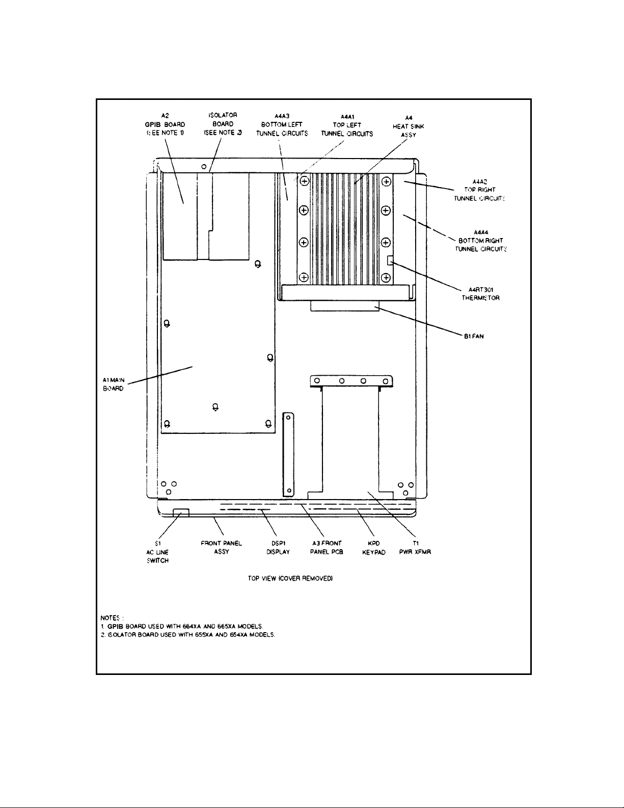
Figure 3-1. Top View with Cover Removed for 655xA & 665xA Models, (Sheet 1 of 2)
32 Troubleshooting
Page 33

Figure 3-1. Top View with Cover Removed for 655xA & 665xA Models, (Sheet 2 of 2)
Troubleshooting 33
Page 34

Table 3-1 Test Equipment Required for Troubleshooting
Type Purpose Recommended Model
GPIB Controller (used only with
models 664xA & 665xA).
Signature Analyzer To troubleshoot most of the primary and
Digital Voltmeter To check various voltage levels. Agilent 3458A
Logic Probe To check data lines. Agilent 545A
Oscilloscope To check wave forms and signal levels. Agilent 54504A/54111A
IC Test Clips To access IC pins. AP Products No. LTC
Ammeter/Current Shunt To measure output current.
To communicate with the supply via the
GPIB interface.
secondary interface circuits
HP Series 200/300
Agilent 5005 A/B
Overall Troubleshooting
Overall troubleshooting procedures for the power supply are given in the flow chart of Figure 3-2. The procedures first
check that neither an AC input, nor a bias supply failure is causing the problem and that the supply passes the turn-on self
test (no error messages). The normal turn-on, self-test indications are described in the "Power-on Checkout" paragraph in
Chapter 3 of the Operating Manual.
If the supply passes the self test, Figure 3-2 directs you to perform the verification procedures in Chapter 2 from the front
panel to determine if any functions are not calibrated or are not operating properly. For models 664xA & 665xA, the
verification tests will also check to see if the supply can be programmed from a GPIB controller. If the supply fails any of
the tests, you are directed to the applicable troubleshooting procedure or flow chart. Signature analysis (SA) is used to
troubleshoot some of the supply’s digital circuits.
Power-On Self-Test
The power-on, self-test sequence consists of tests of the front panel, primary GPIB interface (for 664xA & 665xA Models
only), secondary interface circuits, and the isolator board (for 654xA & 655xA models). If the supply fails the self test, the
output will remain disabled (turned off) and the front panel display should indicate the type of failure. The error will be
displayed indefinitely and the supply will not accept GPIB or front panel commands.
Note that in order to perform troubleshooting procedures that require you to program the supply, you will have to disable
the self test. You can do this by turning the supply off after it has failed the self test, and by holding down the "7" key on the
front panel for two seconds while turning the unit on. This will cause the supply to skip the power-on self test. Table 3-2
lists the self test error messages that can appear on the display and gives the probable cause for each error.
Note For models 664xA & 665xA, a partial self test is performed when the *TST? query is executed (see Table
3-2). Those tests that interfere with normal interface operation or cause the output to change are not
performed by *TST?. The return value of *TST? will be zero if all tests pass, or the error co de of the first
test that failed. The supply will not display error codes and will continue to attempt normal operation if
*TST? returns a nonzero value.
34 Troubleshooting
Page 35

Signature Analysis
The easiest and most efficient method of troubleshooting microprocessor based instruments is signature analysis (SA).
The SA technique is similar to signal tracing with an oscilloscope in linear circuits. Part of the microprocessor memory is
dedicated to signature analysis and a known bit stream is generated to stimulate as many nodes as possible within a circuit.
However, because it is virtually impossible to analyze a bit stream with an oscilloscope, a signature analyzer is used to
compress the bit stream into a four character signature. By comparing the signatures of the IC under test to the correct
signatures for each node, faults can be isolated to one or two components.
Signature analysis tests are provided for some of the digital circuits on the front panel board, the secondary interface circuits
on the main circuit board, and for models 664xA & 665xA, the GPIB (primary interface) board. The GPIB primary
interface SA tests are given in Table 3-3, SA tests for the front panel are given in Table 3-4, and the secondary interface SA
tests are given in Tab l e 3-5.
References are made to the appropriate SA table from the troubleshooting flow charts or procedures. The following general
rules apply to signature analysis testing.
1. Be sure to use the correct test setup connections for the specific test.
2. Note the signatures for Vcc (+ 5 V) and common on the IC being examined. If an incorrect signature is the same as that
of Vcc or common, that pin (or point in the circuit) is probably shorted to Vcc or ground.
3. If two pins have identical signatures, they are probably shorted together.
4. If two signatures are similar, it is only a coincidence.
5. If a signature is incorrect at an input pin, but is correct at its source (e.g., output of previous IC), check for printed
circuit track or soldering problems.
6. An incorrect signature at an output could be caused by a faulty component producing the output. It can also be caused
by an input short circuit in another component on the board.
Note After completing an SA test, you must exit the SA mode by turning off power and performing a power-on
reset.
Troubleshooting 35
Page 36

Table 3-2 Self Test Error Codes/Messages
Code/Message Description Probable Cause
El FP RAM Front panel RAM test failed
(power-on).
E2 FP ROM Front panel ROM test failed
(power-on, and for models 664xA &
665xA, also *TST?).
E3 EE CHKSM Front panel EEPROM checksum test
failed (power-on, and for models
664xA & 665xA, also *TST?).
The following four items (E4-E7) apply only to Agilent models 664xA & 665xA supplies.
E4 PRI XRAM Primary interface external RAM test
failed (power-on).
E5 PRI IRAM Primary interface internal RAM test
failed (power-on).
E6 PRI ROM Primary interface ROM test failed
(power-on, and for models 664xA &
665xA, also *TST?).
E7 GPIB GPIB interface test failed (power-on). Talker/listener chip A2U117 defective.
E8 SEC RAM Secondary interface RAM test failed
(power-on).
E9 SEC ROM Secondary interface ROM test failed
(power-on, and for models 664xA &
665xA, also *TST?).
El0 SEC 5 V Secondary interface 5 volt read back
test failed (power-on, and for models
664xA & 665xA, also *TST?).
E11 TEMP Ambient temperature read back test
failed power-on, and for models
664xA & 665xA, also *TST?).
E12 DACS CV or CC DAC tests failed
(power-on).
Note: The following error messages can appear due to a failure occurring either while the power supply is operating or
during the self test.
SERIAL TIMEOUT Serial data line failure on GPIB or
isolator board.
SERIAL DOWN Serial data line failure on GPIB or
isolator board.
UART PARITY UART failed. UART chip A2U112 defective.
UART FRAMING UART failed. UART chip A2U112 defective.
UART OVERRUN UART failed. UART chip A2U112 defective.
SBUF OVERRUN Serial buffer failure. UART chip A2U112 defective or GPIB board is in
SBUF FULL Serial buffer failure. UART chip A2U112 defective or GPIB board is in
EE WRITE ERR EEPROM write failure. EEPROM A3U6 defective or calibration error.
SECONDARY DN Serial data line failure on main board
or isolator board.
Microprocessor A3U3 defective.
ROM A3U4 or address latches A3U8 defective.
Possibly due to power loss during a write operation.
See Checksum Error Recovery in the Operating
Manual. If power loss is not the problem, EEPROM
A3U6 could be defective (after replacing U6, supply
must be initialized and calibrated).
RAM A2U108 defective.
Microprocessor A2U114 defective.
ROM A2U106 defective.
Microprocessor AlU504 defective.
Microprocessor AlU504 defective.
Comparators AlU513, read back DAC
AlU511/U512, or secondary bias supply defective.
Thermistor AlRT770 or comparator AlU513
defective
CV DAC AlU507/U508 or CC DAC
AlU509/U510 defective (see Figure 3-10).
See Figure 3-13.
See Figure 3-13.
SA mode.
SA mode.
See Figure 3-14.
36 Troubleshooting
Page 37

Figure 3-2. Overall Troubleshooting Flow Diagram (Sheet 1 of 4)
Troubleshooting 37
Page 38

38 Troubleshooting
Figure 3-2. Overall Troubleshooting Flow Diagram (Sheet 2 of 4)
Figure 3-2. Overall Troubleshooting Flow Diagram (Sheet 3 of 4)
Page 39

Troubleshooting 39
Page 40

40 Troubleshooting
Figure 3-2. Overall Troubleshooting Flow Diagram (Sheet 4 of 4)
Page 41

Firmware Revisions (for Models 664xA & 665xA)
You can use the *IDN? query to identify the revision of the supply’s firmware. The query will readback the revisions of the
primary ROM A2U106, the front panel ROM A3U4, and the secondary microprocessor AlU504. The manufacturer and
model number of the supply are also returned. The following is a sample program:
10 ALLOCATE L$[52]
20 OUTPUT 705;"*IDN?"
30 ENTER 705;L$
40 DISP L$
50 END
The computer will display the manufacturer’s name, the model number, a "0," and then the firmware revisions.
Example:"AGILENT TECHNOLOGIES,6651A,0,fA.01.05sA.01.02pA.01.05"
where,
pA.01.05 is the primary interface (p) firmware revision (see Table 3-3).
fA.01.05 is the front panel (f) firmware revision (see Table 3-4).
sA.01.02 is the secondary interface (s) firmware revision (see Table 3-5).
For Agilent models 654xA & 655xA, the revision level of the ROMs can be found on the label affixed to the physical IC
chip itself.
Test Headers
For Agilent models 664xA & 665xA, there are two test header connectors; A3J3 and A2J106. The A3J3 connector is
located on the A3 front panel board and the A2J106 connector is located on the A2 GPIB board (see Figure 3-3). They are
accessible when the top cover is removed from the supply. For models 654xA & 655xA, only the A3J3 test header is used.
Figure 3-3. Test Header Jumper Positions
Troubleshooting 41
Page 42

Front Panel Test Connector A3J3 Pins Description
1 and 2 (SA MODE) With these pins jumpered, the front panel is placed in the SA mode.
Removing the jumper takes the front panel out of the SA mode.
3 and 4 (INHIBIT CAL) With these pins jumpered, the power supply will ignore calibration
commands, thus providing security against unauthoriz ed calibration. With
the jumper removed, the power supply will respond to calibration
commands.
5 and 6 (FACTORY PRESET CAL) With these pins jumpered, the power supply’s calibration constants are set to
their factory preset values. This can be useful if you have trouble calibrating
the unit or if you forget the calibration password. See the "POST REPAIR
CALIBRATION" discussion later in this chapter.
7 and 8 (NORM) This is the normal operating/storage position for the jumper.
Primary Interface Test Connector
A2J106 Pins, For Agilent Models 664xA
& 665xA Only
1 and 2 (SA MODE) With these pins jumpered, the primary interface is placed in the SA mode.
3 and 4 (DIG I/O) *With these pins jumpered, the supply’s Digital Control (DIG CNTL) port is
5 and 6 (RELAY LINK) *With these pins jumpered, the DIG CNTL port is configured to provide
7 and 8 (FLT/INH) *With these pins jumpered (as shipped from the factory), the DIG CNTL
*See Appendix D in the Operating Manual for more information.
Description
Removing this jumper takes the primary interface out of the SA mode.
configured to be used with custom digital interface circuits.
relay control outputs for relay accessories.
port is configured to provide a fault indicator (FLT) output and a remote
inhibit (RI) input.
42 Troubleshooting
Page 43

Figure 3-4. Connections For A2 GPIB Board Models 664xA & 665xA Only (Sheet 1 of 3)
Troubleshooting 43
Page 44

Figure 3-4. Connections For A2 GPIB Board Models 664xA & 665xA Only (Sheet 2 of 3)
44 Troubleshooting
Page 45

Figure 3-4. Connections For A2 GPIB Board Models 664xA & 665xA Only (Sheet 3 of 3)
Troubleshooting 45
Page 46

Table 3-3. Primary Interface SA Test
Description: These signatures check some primary interface circuits on the A2 GPIB Board.
Valid A2U106 ROM Firmware Revision: A.01.06
Test Setup: See Figure 3-4 Sheet 1.
1. Turn off the power supply and remove the top cover.
2. Connect SA jumper of connector JlO6 on A2 Agilent board to pins 1 and 2. Remember the original jumper position as
you will need to restore the jumper to its original position after this test.
3. Connect signature analyzer CLOCK, START, STOP, and GROUND inputs as shown below.
Signature Analyzer Edge A2 Board Connection
Input Setting
4. Turn on the power supply and u the signature analyzer probe to take the following signatures:
Power: 5 V = 9FFP
Serial Link: A2U109-3 = 0l04
Microprocessor: A2Ul14-24 = 9FFP
A2U114-25 = UF39
Digital Control Interface:A2U118-1 = 9AFI
A2U118-9 = 40A5
A2U118-10 = l029
A2U118-15 = 00l0
A2U118-16 = 040A
Gated Array Logic: A2U119-2 = 0A55
A2U119-5= 0040
A2U119-15 = 0040
5. After completing the tests, be sure to return the J106 jumper to its original position.
46 Troubleshooting
Page 47

Table 3-4. Front Panel SA Test
Description: These signatures check microprocessor A3U3 on the front panel board.
Valid A3U4 ROM Firmware Revision: A.01.07
Test Setup: See Figure 3-4 Sheet 2 (for 200 Watt) or Sheet 3 (for 500 Watt) supplies.
1. Turn off the power supply and remove the top cover.
2. To gain access to A3 Front Panel Board, perform steps (a) and (b) of the disassembly procedure for Front Panel
Assembly (See “Disassembly Procedures” later in this chapter).
3. Connect SA jumper between pins 1 and 2 of connector J3 on A3 Front Panel board. Remember the original jumper
position as you will need to restore the jumper to its original position after this test.
4. Connect signature analyzer CLOCK, START, STOP, and GROUND inputs. Be sure to unplug the cable from J2 in
order to access the connector pins.
Signature Analyzer Edge A3 Front Panel Board
Input Setting Connection
J2-8
5. Turn on the power supply and use the signature analyzer probe to take the following signatures:
Power: 5 V = 3395
Microprocessor: A3U3-15 = 0000 A3U3-29 = l029
A3U3-19 = 552U A3U3-30 = 0295
A3U3-20= 954C A3U3-31 = 0000
A3U3-21 = A552 A3U3-32 = 3395
A3U3-22= 2954 A3U3-33= 0008
A3U3-23 = 0A55 A3U3-34 = 040A
A3U3-24 = 3395 A3U3-35 = 0l02
A3U3-25 = 3395 A3U3-38 = 0002
A3U3-26= 0000 A3U3-39= 0020
A3U3-27= 0000 A3U3-42= 0000
A3U3-28 = 40A5
6. After completing the test, be sure to return the J3 jumper to its original position.
Troubleshooting 47
Page 48

Table 3-5. Secondary Interface SA Test
Description: These signatures check the secondary microprocessor AlU504.
Valid AlU504 ROM Firmware Revision: A.01.03
Test Setup: See Figure 3-4 either Sheet 2 or Sheet 3 as applicable to your model.
1. Turn off the power supply and remove the top cover.
2. Connect signature analyzer CLOCK, START, STOP, and GROUND inputs and setup as follows:
Signature Analyzer Edge A1 Board Connection
Input Setting
3. To place the secondary interface in the SA mode, turn on the power supply while momentarily (for 2 seconds) shorting
A1U504-1 to A1U504-20 (common).
4. Use the signature analyzer probe to take the following signatures:
Power: 5 V = 1C4C
Microprocessor: AlU504-1 = F77H AlU504-21 = 5PC7
AlU504-2 = C98P AlU504-22 = 5PC7
AlU504-3 = 1573AlU504-23 = 5PC7
AlU504-4 = P42A AlU504-24 = 6CAP
AlU504-5 = UHF8 AlU504-25 = A319
AlU504-6 = F5UC AlU504-26 = A319
AlU504-7 = UH8C AlU504-27 = A319
AlU504-8 = 23UC AlU504-28 = 5PC7
AlU504-9 = 0000AlU504-29 = 1C4C
AlU504-10= 1C4C AlU504-30= 0000
AlU504-11 = 1C4C AlU504-31 = 1C4C
AlU504-12 = C76F AlU504-32 = 0000
AlU504-13= U042 AlU504-33 = 0000
AlU504-14 = 2189 AlU504-34 = 0000
AlU504-15 = 1C4C AlU504-35 = 0004
AlU504-16 = 1C45 AlU504-36 = 0UP7
AlU504-17 = 0010 AlU504-37 = UF7P
AlU504-18 = 0000 AlU504-38 = CP47
AlU504-19 = 1C4C AlU504-39 = CP47
AlU504-20 = 0000 AlU504-40 = 1C4C
5. After completing the tests, be sure to return the J3 jumper to its original position.
48 Troubleshooting
Page 49

Troubleshooting Procedures
Flow Charts
Troubleshooting flow charts for various circ uits are given in Figures 3-5 through 3 -l0 and 3-12 through 3-16. The
appropriate flow chart is used when a particular trouble symptom has been encountered during the self test (see Table 3-2)
or when performing the overall troubleshooting procedures (see Figure 3-2). Many flow charts make reference to the test
points listed in Chapter 6. The circuit locations of the test points are shown on the schematics. Test point locations are
shown on the component location diagrams in Chapter 6.
Figure 3-5 isolates the fault to components on the GPIB or Isolator board or the front panel board when the display is
inoperative. Figures 3-6 and 3-7 isolate the problem for OV circuit trouble symptoms. Figures 3-8 and 3-9 provide
troubleshooting for output held low and output held high trouble symptoms, respectively. Figure 3-10 troubleshoots the
DAC circuits. Waveforms which will aid you in troubleshooting the CV and CC DAC circuits are provided in Figure 3-11.
Figure 3-12 isolates faults to either the DAC or the amplifier component in CV and CC DAC/amplifier circuits. Figures
3-13 and 3-14 provide troubleshooting procedures for the GPIB board (664xA & 665xA), the isolator board (654xA &
655xA), and the main board, respectively, when serial data line or secondary interface error messages appear on the display.
Figure 3-15 is for the down programming circuit and Figure 3-16 is the Isolator Board circuits troubleshooting chart.
Bias and Reference Supplies
Many of the troubleshooting flow charts start by checking the bias and/or reference voltages to make sure that they are not
causing the problem. Table 6-3 in Chapter 6 lists the bias and the reference voltage test points for the A2 GPIB board, A2
Isolator Board, and the A1 Board.
CV/CC Status Annunciators Troubleshooting
When troubleshooting the CV/CC status annunciators or the status readback circuits, first measure the voltage dro p across
the gating diodes; D651 (CC) and D615 (CV). A conducting diode indicates an active (ON) control circuit. This forward
drop is applied to the input of the associated status comparator (U608) and drives the output low. The low signal indicates
an active status which is sent to the secondary microprocessor U504 through U502. The front panel CV annunciator
indicates when the CV mode is active (CV* is low). The front panel CC annunciator indicates when the CC mode is active
(CC* is low). The UNREGULATED (Unr) annunciator c omes on when neither the CV nor CC is active.
Post Repair Calibration
Calibration is required annually and whenever certain components are replaced. If components in any of the circuits listed
below are replaced, the supply must be re-calibrated as described in Appendix A of the Operating Manual.
A1 Main Board: CV/CC DACs/operational amplifiers, CV/CC control circuit amplifiers, readback DAC/operational
amplifier, readback comparators, or DAC reference circuits.
A3 Front Panel Board: If the front panel board A3 or the EPROM chip A3U6 is replaced, the supply must be initialized first
(see "EEPROM INITIALIZATION" later in this chapter) and then be recalibrated as described in Appendix A in the
Operating Manual.
Inhibit Calibration Jumper
If "CAL DENIED" appears on the display when the front panel calibration is attempted, or if error code 1 occurs when
GPIB calibration (models 664xA & 665xA) is attempted, the INHIBIT CAL jumper (see Figure 3-3) has been installed.
This prevents power supply calibration from being changed. You must remove this jumper from the INHIBIT CAL position
Troubleshooting 49
Page 50

(between pins J3-3 and J3-4) and return it to the NORM position (between pins J3-7 and J3 -8) in order to calibrate the
supply.
Calibration Password
In order to enter the calibration mode, you must use the correct password as described in Appendix A of the Operating
Manual. As shipped from the factory, the supply's model number (e.g., “6652”) is the password. If you use an incorrect
password, "PASSWD ERROR" will appear on the display for front panel calibration (or error code 2 occurs for GPIB
calibration) and the calibration mode will not be enabled.
If you have changed the password and have forgotten it, you can re cover the calibration function by restoring the factor y
preset calibration constants. To do this, proceed as follows:
a. Turn off the supply and remove the top cover.
b. Install jumper in test header J3 on the front panel board A3 in the FACTORY PRESET CAL position between pins
J3-5 and J3-6. (See Figure 3-3.)
c. Turn on the supply and note that "ADDR 5" and then "PWR ON INIT" appear briefly on the front panel display.
d. When "PWR ON INIT" no longer appears on the display, the supply's factory calibration constants have been restored
and the password has been changed to "0" defeating password protection. You can now turn off the supply, remove the
jumper and return it to the NORM position between pins J3-7 and J3-8. (See Figure 3-3.)
e. Turn on the supply. At this point you can set a new password (if desired) and recalibrate the supply as described in
Appendix A of the Operating Manual.
50 Troubleshooting
Page 51

Figure 3-5. No Display Troubleshooting
Troubleshooting 51
Page 52

52 Troubleshooting
Figure 3-6. OV Will Not Fire Troubleshooting
Page 53

Figure 3-7. OV At Turn-On Troubleshooting (Sheet 1 of 2)
Troubleshooting 53
Page 54

54 Troubleshooting
Figure 3-7. OV At Turn-On Troubleshooting (Sheet 2 of 2)
Page 55

Figure 3-8. Output Held Low Troubleshooting (Sheet 1 of 2)
Troubleshooting 55
Page 56

56 Troubleshooting
Figure 3-8. Output Held Low Troubleshooting (Sheet 2 of 2)
Page 57

Figure 3-9. Output Held High Troubleshooting
Troubleshooting 57
Page 58

58 Troubleshooting
Figure 3-10. DAC Circuits Troubleshooting
Page 59

Figure 3-11. DAC Waveforms
Figure 3-12. CV/CC DAC and Amplifier Troubleshooting
Troubleshooting 59
Page 60

60 Troubleshooting
Figure 3-13. Serial Down Troubleshooting (Sheet 1 of 2)
Figure 3-13. Serial Down Troubleshooting (Sheet 2 of 2)
Page 61

Troubleshooting 61
Page 62

62 Troubleshooting
Figure 3-14. Secondary Down Troubleshooting (Sheet 1 of 2)
Page 63

Figure 3-14. Secondary Down Troubleshooting (Sheet 2 of 2)
Troubleshooting 63
Page 64

64 Troubleshooting
Figure 3-15. Slow Down Programming Troubleshooting
Page 65

Figure 3-16. Isolator Board Circuits Troubleshooting
Troubleshooting 65
Page 66

EEPROM Initialization
EEPROM chip A3U6 on the front panel board stores the supply’s GPIB address and model number as well as other
constants which are required to program and calibrate the supply. The EEPROM was initialized with the proper constants
before the supply was shipped from the factory. If the front panel board, A3, or the EEPROM chip, A3U6, is replaced, the
supply must be reinitialized with the proper c onstants by running the program listed in Figure 3-17.
The program will pause and prompt you to select either "Initialization (I)" or "Factory Preset Replacement (F)." You must
select "I" in order for the pr ogram to continue and initialize the supply. After the supply has been initialized using this
program, it must be calibrated as described in Appendix A of the operating Manual. After calibration has been completed,
you should transfer the calibration constants to the new EPROM’s "Factory Cal" locations as described below.
Note If the EEPROM (A3U6) or the front panel board is replaced, the EEPROM must be reinitialized. For
models 654xA & 655xA, a separate GPIB board can be installed temporarily in place of the A2 Isolator
Board in order to perform the reinitialization.
For 664xA & 665xA models, the program in Figure 3-17 can be run to reinitialize the supply. This
program contains statements for several different Agilent models. You can shorten and thus customize this
program for just your specific model by deleting the statements from this program listing that apply to
models that you do not use.
Transferring Calibration Constants Into Factory Preset Locations
This will allow you to recover the new calibration constants using the FACTORY PRESET CAL jumper as described
previously. Being able to recover the calibration constants could be important in the future if you have trouble calibrating
the supply. Having the FACTORY PRESET CAL constants available, will allow you to operate the supply and/or
re-calibrate as required. After you have initialized and calibrated the supply, transfer the calibration constants into the
FACTORY PRESET CAL locations, by again running the program listed in Figure 3-17. This time when the program
pauses for you to make the selection, select “Factory Preset Replacement (F)”. After you select "F," the program will
continue and transfer the newly obtained calibration constants into the proper locations o f the new EEPROM.
66 Troubleshooting
Page 67

10 ! Program to initialize EEPR0M or move factory preset data in 654xA,
20 ! 664xA, 655xA and 665xA power supplies.
30 ! RE-ST0RE "INIT_ps"
40 ! Rev A.00.00 dated Mar 30, 1993
50 !
60 DIM Init_data(1:45),Model$[5],Idn$[21],Cal_data$[40]
70 INTEGER Addr(1:45),Length(1:45)
80 ASSIGN @Ps TO 705 ! Supply must be at address 705
90 CLEAR SCREEN
100 !
110 Eprom_data_addr: ! Data address
120 DATA 2,6,10,14,18,19,20,24,28,32
130 DATA 36,37,38,42,46,50,54,55,56,57
140 DATA 64,68,72,76,80,150,152,153,154,155
150 DATA 156,158,160,162,163,164,165,166,167,168
160 DATA 169,170,171,172,174
170 !
180 Eprom_data_len: ! Data for word length
190 DATA 4,4,4,4,1,1,4,4,4,4
200 DATA 1,1,4,4,4,4,1,1,1,1
210 DATA 4,4,4,4,4,2,1,1,1,1
220 DATA 2,2,2,1,1,1,1,1,1,1
230 DATA 1,1,1,2,1
240 !
250 Eprom_data_6x41: ! ! EEPROM data for 6541A and 6641A
260 DATA 468.3,16.6,8.19,0,83,0,177,140,20.475,0
270 DATA 99,1,78.25,78.25,8.8,0,83,255,20,10
280 DATA 6541,456.09,168.18,182,168.18,1768,5,255,0,0
290 DATA 16,6541,0,20,180,20,180,156,37,26
300 DATA 120,15,20,0,4
310 !
320 Eprom data_6x42: ! ! EEPROM data for 6542A and 6642A
330 DATA 195.534,4.434,20.475,0,83,0,354,140,10.238,0
340 DATA 99,1,42.512,17.75,22,0,83,255,20,10
350 DATA 6542,167,156,365,156,1768,5,255,0,0
360 DATA 16,6542,0,20,180,20,180,156,37,26
370 DATA 120,15,20,0,4
380 !
390 Eprom_data_6x43: ! ! EEPROM data for 6543A and 6643A
400 DATA 111,16.6,35.81,0,83,0,587,140,6.143,0
410 DATA 99,1,18.68,78.75,38.5,0,83,255,20,10
420 DATA 6543,104.3,171.7,607,164.2,1768,5,255,0,0
430 DATA 16,6543,0,20,180,20,180,156,37,26
440 DATA 120,15,20,0,4
450 !
460 Eprom_data_6x44: ! ! EEPR0M data for 6544A and 6644A
470 DATA 64.8,16.6,61.425,0,83,0,1010,136.86,3.583,0
480 DATA 99,1,10.43,78.2,66,0,83,255,20,10
490 DATA 6544,60.81,168.18,1044,168.18,1768,5,255,0,0
500 DATA 16,6544,0,20,180,20,180,156,37,26
510 DATA 120,15,20,0,4
Figure 3-17. Initialization and Factory Preset Replacement Program Listing (Sheet 1 of 6)
Troubleshooting 67
Page 68

520 !
530 Eprom_data_6x45: ! ! EEPROM data for 6545A and 6645A
540 DATA 32.42,16.6,122.85,0,82,0,2358,140,1.537,0
550 DATA 100,1,5.313,117.38,132,0,82,255,20,10
560 DATA 6545,30.41,168.18,2436,168.18,1768,5,255,0,0
570 DATA 16,6545,0,20,180,20,180,156,37,26
580 DATA 186,15,20,0,4
590 !
600 Eprom_data_6x51: ! ! EEPR0M data for 655lA and 6651A
610 DATA 486.3,16.6,8.19,0,83,0,70.16,136.86,51.188,0
620 DATA 99,1,78.25,78.25,8.8,0,83,255,20,10
630 DATA 6551,456.09,168.18,72.47,168.18,1768,5,255,0,0
640 DATA 16,6551,0,20,180,20,180,156,37,26
650 DATA 186,15,20,0,4
660 !
670 Eprom_data_6x52: ! ! EEPR0M data for 6552A and 6652A
680 DATA 195.534,4.434,20.475,0,83,0,141.87,97.29,25.594,0
690 DATA 99,1,42.512,17.75,22,0,83,255,20,10
700 DATA 6552,167,156,130,156,1768,5,255,0,0
710 DATA 16,6552,0,20,180,20,180,156,37,26
720 DATA 186,15,20,0,4
730 !
740 Eprom_data_6x53: ! ! EEPR0M data for 6553A and 6653A
750 DATA 111,16.35,35.831,0,83,0,224,127,15.356,0
760 DATA 99,1,18.68,79.5,38.5,0,83,255,20,10
770 DATA 6553,104.3,171.7,231.8,164.2,1768,5,255,0,0
780 DATA 16,6553,0,20,180,20,180,156,37,26
790 DATA 186,15,20,0,4
800 !
810 Eprom_data_6x54: ! ! EEPR0M data for 6554A and 6654A
820 DATA 64,16.35,61.425,0,83,0,393,127,9.214,0
830 DATA 99,1,10.43,78.2,66,0,83,255,20,10
840 DATA 6554,60.81,168,405.41,168.18,1768,5,255,0,0
850 DATA 16,6554,0,20,180,20,180,156,37,26
860 DATA 186,15,20,0,4
870 !
880 Eprom_data_6x55: ! ! EEPR0M data for 6555A and 6655A
890 DATA 32.42,16.6,122.85,0,82,0,882.98,136.86,4.095,0
900 DATA 100,1,5.313,117.38,132,0,82,255,20,10
910 DATA 6555,30.41,168.18,912.18,168.18,1768,5,255,0,0
920 DATA 16,6555,0,20,180,20,180,156,37,26
930 DATA 186,15,20,0,4
940 !
950 INPUT "Input Power Supply model number. Example:""6641A""",Model$
960 Model$=TRIM$(UPC$(Model$))
970 CLEAR SCREEN
980 !
990 RESTORE Eprom_data_addr
1000 !
1010 FOR I=1 T0 45
1020 READ Addr(I)
Figure 3-17. Initialization and Factory Preset Replacement Program Listing (Sheet 2 of 6)
68 Troubleshooting
Page 69

1030 NEXT I
1040 !
1050 RESTORE Eprom_data_len
1060 !
1070 FOR I=1 T0 45
1080 READ Length(I)
1090 NEXT I
1100 !
1110 SELECT Model$
uppercase
1120 !
1130 CASE "6541A"
1140 RESTORE Eprom_data_6x41
1150 CASE "6542A"
1160 RESTORE Eprom_data_6x42
1170 CASE "6543A"
1180 RESTORE Eprom_data_6x43
1190 CASE "6544A"
1200 RESTORE Eprom_data_6x44
1210 CASE "6545A"
1220 RESTORE Eprom_data_6x45
1230 !
1240 CASE "6641A"
1250 RESTORE Eprom_data_6x41
1260 CASE "6642A"
1270 RESTORE Eprom_data_6x42
1280 CASE "6643A"
1290 RESTORE Eprom_data_6x43
1300 CASE "6644A"
1310 RESTORE Eprom_data_6x44
1320 CASE "6645A"
1330 RESTORE Eprom_data_6x45
1340 !
1350 CASE "6551A"
1360 RESTORE Eprom_data_6x51
1370 CASE "6552A"
1380 RESTORE Eprom_data_6x52
1390 CASE "6545A"
1400 RESTORE Eprom_data_6x53
1410 CASE "6554A"
1420 RESTORE Eprom_data_6x54
1430 CASE "6555A"
1440 RESTORE Eprom_data_6x55
1450 !
1460 CASE "6651A"
1470 RESTORE Eprom_data_6x51
1480 CASE "6652A"
1490 RESTORE Eprom_data_6x52
1500 CASE "6653A"
1510 RESTORE Eprom_data_6x53
1520 CASE "6654A"
Figure 3-17. Initialization and Factory Preset Replacement Program Listing (Sheet 3 of 6)
Troubleshooting 69
Page 70

1530 RESTORE Eprom_data_6x54
1540 CASE "6655A"
1550 RESTORE Eprom_data_6x55
1560 !
1570 CASE ELSE
1580 PRINT "Model number not found. Program is for Agilent models"
1590 PRINT "6541A, 6542A, 6543A, 6544A and 6545A"
1600 PRINT "6641A, 6642A, 6643A, 6644A and 6645A"
1610 PRINT "6551A, 6552A, 6553A, 6554A and 6555A"
1620 PRINT "6651A, 6652A, 6663A, 6654A and 6655A"
1630 STOP
1640 END SELECT
1650 !
1660 FOR I=1 T0 45 ! Read model dependent data
1670 READ Init_data(I)
1680 IF I=21 0R I=32 THEN Init_data(I)=VAL(Model$)
1690 NEXT I
1700 !
1710 OUTPUT @Ps;"*CLS" ! Clears power supply registers
1720 !
1730 OUTPUT @Ps;"CAL;STATE ON," ! Turn on cal mode, "0" passcode
1740 !
1750 G0SUB Ps_error ! Error if passcode is not "0"!
1760 IF Err THEN
1770 OUTPUT @Ps;"*IDN?" ! Get data from model # location
1780 ENTER @Ps;Idn$
1790 Model=VAL(Idn$[POS(Idn$,",")+1] )
1800 ELSE
1810 GOTO Start
1820 END IF
1830 !
1840 OUTPUT @Ps;"CAL:STATE ON,";Model ! Turn on cal mode, passcode =
1850 ! data at model number location
1860 !
1870 G0SUB Ps_error ! Error if passcode is not same as
1880 ! data at model & location
1890 IF Err THEN
1900 OUTPUT @Ps;"CAL:STATE ON,";Model$[1,4] ! Turn on cal mode, passcode =
1910 ! model #
1920 GOSUB Ps_error
1930 IF Err THEN
1940 PRINT "Change pass code to the power supply model # or zero then restart the program."
1950 STOP
1960 ELSE
1970 GOTO Start
1980 END IF
1990 END IF
2000 !
2010 Start: !
2020 !
Figure 3-17. Initialization and Factory Preset Replacement Program Listing (Sheet 4 of 6)
70 Troubleshooting
Page 71

2030 !
2040 INPUT "Select Initialization (I) or Factory preset replacement (F).",Sel$
2050 CLEAR SCREEN
2060 SELECT (UPC$(Sel$))
2070 CASE "I" ! Select Initialization
2080 GOTO Init_eeprom
2090 CASE "F" ! Select install new factory data
2100 GOTO Fact_preset
2110 CASE ELSE
2120 BEEP
2130 GOTO Start
2140 END SELECT
2150 !
2160 Init_eeprom: !
2170 PRINT "Initializing EEPROM"
2180 !
2190 FOR I=1 TO 45
2200 OUTPUT @Ps;"DIAG:EEPR '';Addr(I);'','';Length(I);'','';Init_data(I)
2210 NEXT I
2220 GOTO Cal_off
2230 !
2240 !
2250 Fact_preset: !
2260 CLEAR SCREEN
2270 PRINT "This program should ONLY be completed if your power supply"
2280 PRINT "EEPROM has been replaced or a component that will effect"
2290 PRINT "the calibration AND the alignment of voltage, overvoltage"
2300 PRINT "and current is complete AND unit has passed the performance"
2310 PRINT "test. Enter C to continue, any other key to abort."
2320 INPUT Cont_prog$
2330 IF (UPC$(Cont_prog$))< >"C" THEN GOTO Cal_off
2340 !
2350 CLEAR SCREEN
2360 PRINT "Transferring calibration data to factory preset locations."
2370 !
2380 Fact_cal_sour: ! Address of factory calibration data source
2390 DATA 2,6,68,72,20,24,76,80,150
2400 !
2410 Fact_cal_dest: ! Address of factory calibration data destination
2420 DATA 84,88,92,96,100,104,108,112,116
2430 !
2440 Fact_cal_len: ! Length of factory calibration data
2450 DATA 4,4,4,4,4,4,4,4,2
2460 !
2470 RESTORE Fact_cal_sour
2480 F0R I=1 TO 9
2490 READ Cal_sour_addr(I)
2500 NEXT I
2510 !
2520 RESTORE Fact_cal_dest
2530 FOR I=1 T0 9
Figure 3-17. Initialization and Factory Preset Replacement Program Listing (Sheet 5 of 6)
Troubleshooting 71
Page 72

2540 READ Cal_dest_addr(I)
2550 NEXT I
2560 !
2570 RESTORE Fact_cal_len
2580 FOR I=1 T0 9
2590 READ Cal_length(I)
2600 NEXT I
2610 !
2620 FOR I=1 T0 9 ! Locations of good data
2630 OUTPUT @Ps;"DIAG:EEPR?";Cal_sour_addr(I);",";Cal_length(I)
Read good data
2640 ENTER @Ps;Cal_data$ ! Enter good data
2650 OUTPUT @Ps;"DIAG:EEPR";Cal_dest_addr(I);",";Cal_length(I);",";Cal_data$ !
Write good data to factory preset locations
2660 NEXT I
2670 !
2680 !
2690 Cal_off
2700 CLEAR SCREEN
2710 OUTPUT @Ps;"CAL:STATE OFF" ! Turn off cal mode
2720 !
2730 GOSUB Ps_error ! Check for errors
2740 IF Err THEN
2750 PRINT "An error occurred during the EEPROM read/write, Check for"
2780 PRINT "programming errors. Initialization data may be incorrect."
2770 STOP
2780 END IF
2790 !
2800 PRINT "Operation complete. Program stopped."
2810 STOP
2820 !
2830 Ps_error: ! Error handling subroutine
2840 OUTPUT @Ps;"SYST:ERR?" ! Check for errors
2850 ENTER @Ps;Err
2860 RETURN
2870 !
2880 END
Figure 3-17. Initialization and Factory Preset Replacement Program Listing (Sheet 6 of 6)
Disassembly Procedures
The following paragraphs provide instructions on how to disassemble various components of the power supply. Once
disassembled, the components can be reassembled by performing the disassembly instructions in reverse order.
SHOCK HAZARD. To avoid the possibility of personal injury, turn on AC power and disconnect the line
cord before removing the top cover. Disconnect the GPIB cable (for 664xA & 665xA models), and
any loads, and remote sense leads before attempting disassembly.
Most of the attaching hardware is metric. Use of other types of fasteners will damage threaded inserts.
Refer to the list of required tools when performing disassembly and replacement.
72 Troubleshooting
Page 73

Figure 3-18. Location of Cable and Connector Locations for 655xA and 665xA Models Only
Troubleshooting 73
Page 74

List of Required Tools
a. lPT and 2PT Pozidriv screwdrivers.
b. Tl0, T15 and T25 Torx screwdrivers.
c. Allen wrench, 0.050 inch.
d. Hex driver, 7 mm.
e. Long nose pliers.
f. Antistatic wrist discharge strap.
Top Cover, Removal & Replacement
a. Using a T25 Torx screwdriver, unscrew the two screws which hold the carrying straps to the power supply, and then
remove the other two screws from the opposite side of the case.
b. To remove the cover, you must first spread the bottom rear of the cover and then push the cover back to disengage it
from the front panel.
c. Slide the cover backward until it clears the rear of the power supply.
Figure 3-19. Location of Carrying Strap Restraining Screws, Power Supply Side View
A2 GPIB Board, Removal & Replacement (for 664xA & 665xA Models Only)
To remove the GPIB board, proceed as follows:
a. Remove the top cover of the power supply as described under, "Top Cover Removal and Replacement ."
b. At the rear of the-power supply, remove the protective standoff piece (directly above the AC power receptacle).
c. Remove the two (2) 7 mm, hex screws that hold the GPIB connector in place.
d. At the rear of the supply, remove the two (2) screws that hold the HB-IB board to the chassis .
e. From the top of the power supply, disconnect the phone cable at connector J107 on the GPIB board (the other end of
this cable goes to the main board).
f. Disconnect the phone cable at connector J108 on the GPIB board (the other end of this cable goes to the front panel
board).
g. Disconnect connector P101 on the GPIB board (the other end of this cable goes to the transformer secondary).
h. Remove the GPIB board from the power supply by gently pulling back on the metal holding clip that holds the front
end of the GPIB board in place.
i. To reinstall the GPIB board, perform the above steps in reverse order.
74 Troubleshooting
Page 75

Figure 3-20. GPIB Connector and GPIB Board Holding Screws, Power Supply Rear View
A2 Isolator Board, Removal & Replacement (for 654xA & 655xA Only)
To remove the Isolator board, proceed as follows:
a. Remove the top cover of the power supply as described under, "Top Cover Removal and Replacement."
b. At the rear of the power supply, locate and remove the two (2) screws that hold the Isolator board to the chassis. You
may need to hold the nuts for these screws stationary while you unscrew the screws. The nuts are on the inside of the
chassis.
c. From the top of the power supply, disconnect the phone cable from connector J800 on the A2 board (the other end of
this cable goes to the main board).
d. Disconnect the phone cable from connector J801 on the A2 board (the other end of this cable goes to the front panel
board).
e. Disconnect connector from J803 on the A2 board (the other end of this cable goes to the transformer secondary).
f. Remove the A2 board from the power supply.
g. To reinstall the Isolator board, perform the above steps in reverse order.
Front Panel Assembly, Removal and Replacement
This procedure removes the front panel assembly from the power supply.
a. Remove the Power Supply Cover as described earlier in, "Top Cover Removal and Replacement . "
b. Locate and carefully peel off the vinyl trim (one strip on each side of front panel assembly) to gain access to the side
screws that secure the front panel assembly to the chassis.
c. Using a T10 Torx screwdriver, unscrew the screws from the side of the front panel.
d. Disconnect the phone cable from connector J6 on the A3 board (the other end of the cable goes to the A2 board).
e. Now move the front panel assembly forward a few inches away from the chassis to gain access to the S1 power switch.
f. Disconnect the wires going to the S1 switch assembly and note the color coding of the wires and the respective pins to
which they connect for subsequent reconnection.
g. The front panel assembly can now be removed from the power supply.
h. To reinstall the front panel assembly, perform the above steps in reverse order.
Troubleshooting 75
Page 76

Figure 3-21. Removing Vinyl Strip from Sides of Front Panel Assembly
S1 Line Switch, Removal and Replacement
a. First remove the front panel assembly as described under, "Front Panel Assembly, Removal and Replacement”.
b. On the front panel assembly, release the switch locking tabs by pressing them inward against the body of the switch,
and then remove the switch.
Note When re-installing this switch be sure that the screened letter "O" is at the top of the switch.
A3 Front Panel Board, Removal and Replacement
First remove the front panel assembly as described under, “Front Panel Assembly, Removal and Replacement”. Once you
have access to the front panel board perform these steps:
Note Be careful not to unscrew the knob set screws too far out as they can easily fall out of the knob and
become lost.
a. Use a small allen wrench (0.050") to loosen the set screws inset in the knobs. Remove knobs and shaft bushings.
b. Remove the holding screw (if installed) that secures the board to the front panel assembly. The screw is located near J4
on the front panel board.
c. In order to remove the board itself from the assembly you must slide the board to the left to disengage the holding clips.
To do this, first lift up the restraining tab on the circuit board and then slide the b oard to the left and lift it out.
d. Disconnect display ribbon connector J2. (The other end of this cable goes to the display panel. DO NOT remove cable
at display end.)
Note When reinstalling the front panel board, be sure to line up the “stripe” of the ribbon cable with pin 1 on
J2.
76 Troubleshooting
Page 77

Figure 3-22. Location of Front Panel Board Holding Screw and Restraining Tab
A1 Main Board
a. Remove the top cover and the A2 board (Isolator or GPIB board).
b. Disconnect all cables going to connectors on the main board.
Note Be sure to mark any or all cables prior to removal so that no mistake is made later when reinstalling
these cables.
c. Disconnect the ground wire between the main board and the chassis. (This wire is secured to the side of the chassis near
the AC input).
d. For 500 watt 6x5xA models only:
Disconnect the following DC power cables from conne ctors on the tunnel boards which are located on Heat
Sink Assembly A4:
• Cables W12 and W14 from J202 on the top left tunnel board (A4A1) and bottom left tunnel
board (A4A2), respectively.
• Cables W16 and W18 from J302 on the top right tunnel board (A4A3) and bottom right tunnel
board (A4A4), respectively.
e. Remove two screws (one on each side, near J691 and J450, respectively) which secure the main board to the chassis.
f. Slide the main board towards the front panel to release it from six chassis mounted standoffs and then lift the board out
of the chassis.
A4 Heatsink Assembly (500 Watt Models 6x5xA Only)
This assembly is comprised of a top heatsink with left (A4A1) and right (A4A3) tunnel boards, a bottom heatsink with left
(A4A2) and right (A4A4) tunnel boards, and a bracket that secures the hea t sink and the cooling fan in the chassis. The top
heatsink assembly slides over and is held by tracks on the bottom heatsink assembly. The bottom heatsink assembly slides
over and is held by tracks on insulated blocks at the bottom of the chassis. To disassemble the heatsink assembly, proceed as
follows:
a. Remove the rear panel.
b. Remove the plastic insulator (between the rear panel and the heatsink assembly). Remember to replace this insulator
when you reassemble the heatsink.
Troubleshooting 77
Page 78

c. Disconnect cables W11/W12 and W15/W16 from connectors J201/J202 and J301/J302 on top left and on top right
tunnel boards, respectively.
d. Remove the top heatsink assembly and the attached tunnel boards by sliding the top assembly towards the re ar and off
of the bottom heatsink assembly. Remove the plastic insulator (between heatsink/fan bracket and the heatsink
assembly). Remember to replace this insulator when you reassemble the heatsink.
e. Disconnect cables W13/W14 and W17/W18 from connectors J201/J202 and J301/J302 on the bottom left and on the
bottom right tunnel boards.
f. Remove the bottom heatsink assembly and the attached tunnel boards by sliding the bottom assembly towards the rear
of the insulated blocks in the chassis.
A4A1 or A4A3 Left Tunnel Board, Removal and Replacement
To separate a left tunnel board from its heatsink, proceed as follows:
Note If desired, you can replace a heatsink mounted transistor (Q201, Q203, Q205 and Q207) without
separating the board from the heatsink. Apply a thermal compound to the heatsink/insulator when
replacing the transistors.
a. Remove the heatsink assembly as described above.
b. Remove the screws (two each) securing transistors Q201, Q203, Q205, and Q207 to the heatsink assembly and the left
tunnel board.
c. Unplug each transistor from the socket on the board and separate the board from the heatsink. Note that transistor Q205
is insulated from the heatsink. Be sure that insulator is installed before replacing Q205.
A4A2 or A4A4 Right Tunnel Board
To separate a right tunnel board from its heatsink, proceed as follo ws:
Note If desired, you can replace a heatsink mounted transistor (Q301, Q303, Q305, or Q307) without
separating the board from the heatsink. Apply a thermal compound to the heatsink/insulator before you
replace any transistors.
a. Remove the heatsink assembly as described above. If you are separating the board from the top heatsink assembly,
unplug the thermistor cable from the J300 connector on the board.
b. Remove the screws (two each) securing transistors Q301, Q303, Q305, and Q307 to the heatsink assembly and the right
tunnel board.
c. Unplug each transistor from the socket on the board and separate the board from the heatsink assembly.
B1 Fan, Removal and Replacement
Remove the top cover as described under, "Top Cover Removal and Replacement".
a. Disconnect the fan cable from J601 on the A1 main board.
b. For 500 watt 6x5xA models only, remove the A4 heatsink assembly as described previously.
c. Remove the screws securing the fan to the heat sink assembly and remove the fan.
T1 Power Transformer, Removal and Replacement
To remove the power transformer, the front panel assembly must first be removed to gain access to the bracket screws that
hold the transformer in place. For 654xA and 664xA models, the A1 Main Board must also be removed. Refer to "A1 Board
and Front Panel Assembly, Removal and Replacement" Instructions as required. Once the front panel assembly (and also Al
main board for 200 Watt models) is removed, proceed as follows:
78 Troubleshooting
Page 79

a. In the supply chassis, remove the two screws (three screws for 6x4xA) securing the transformer to the bottom of the
chassis.
b. At the front of the chassis, remove the two screws securing the transformer to the chassis.
c. Use long nose pliers to disconnect all wires going to the transformer terminals.
d. Lift the transformer out of the chassis.
Note The AC power connections at the transformer secondary are model dependent. Be sure to note the color
code of the wires and the respective terminals the wires connect to for subsequent reconnection.
Figure 3-23. Location of XFMR Holding Bracket at Bottom of Chassis
Figure 3-24. Location of XFMR Holding Screws, Inside View
Troubleshooting 79
Page 80

Page 81

4
Principles of Operation
Introduction
This section describes the different functional circuits used in the power supply models covered in this manual. The topics
are presented in the following order: First, the I/O external signals that connect to the Agilent power supply are described.
Next, the overall block diagram for the power supply is described, and last, each functional block shown in the overall block
diagram is discussed in detail.
I/O INTERFACE SIGNALS
Figure 4-1 shows the interface signals between the power supply and the end user (or other external circuits and devices).
Table 4-1 describes these interface signals.
Figure 4-1. Agilent Power Supply, I/O Interface Diagram
Principles of Operation 81
Page 82

Table 4-1. Power Supply Interface Signals
Pin Signal Description
Busbar or terminal strip screw
Output Power Connections
+OUT
1
terminals
-OUT
7-Pin I/O Analog Connector
Pin 1
Pin 2
Pin 3
Pin 4
Pin 5
Pin 6
Pin 7
IP
VP
+Imon
-Imon
ÏP
+S
-S
Rx/Tx Serial Link (Used with GPIB Models 664xA and 665xA only)
J1 and J2 Connectors wired in
parallel (daisy chain fashion)
3-lines; Rx, Tx, and common signals for
both Jl and J2 connectors.
AC Input Power Source
AC power connector, J451 Can be 100 V AC, 120 V AC, 220 V AC or
240 V AC
Positive DC output voltage
Negative DC voltage (or return)
Current Programming
Voltage Programming
External Current Monitor
External Current Monitor
Programming Common
+Sensing Terminal
2
-Sensing Terminal
3
Jl and J2 are telephone connectors.
Input AC power
TB101 Digital Control (DIG CNTL) for 664xA and 665xA Models only
Pins 1 through 4 Pins 1 through 4 can supply one of three
sets of signals
See Table 4-2 for these I/O signals
and pin destinations.
GPIB Interface Connector (Used With Agilent Models 664xA and 665xA only)
GPIB IEEE multi-pin connector signals. See
Chapter 6, Figure 6-3, Sheet 2 (Zone 8A)
for these signals.
1
For the 500 watt Agilent 655xA and 665xA models, the +OUT and -OUT signals connect to bus-bar type, screw
IEEE 488 type connector provides
the interface between an external
computer and the GPIB board.
terminals . For the 200 watt Agilent 654xA and 664xA models, these connections are made at a terminal strip on the
power supply.
2
A switch on the A1 Main Board selects either "Remote" sensing or "Local" sensing of the output voltages (+OUT and
-OUT) leads to be monitored.
3
The Rx and Tx serial link permits up to 16 Agilent power supplies to be connected in a daisy chain fashion, each with its
own unique programmed device address. One GPIB address with other units being subaddressed.
82 Principles of Operation
Page 83

Table 4-2. Digital CNTL Signals
PIN Digital I/O Relay Link Fault/Isolation
Pin 1 OUT 0 RLY SEND FLT Output
Pin 2 OUT 1 NC FLT Common
Pin 3 IN/OUT 2 RLY RTN INH Input
Pin 4 Common Common INH Common
Overall Block Diagram (Figure 4-2)
All of the Agilent Technologies power supplies covered in this service manual consist of four major functional circuit
groups. They are:
1. Secondary Interface Circuits on the A1 Main Board. .
2. Output Power and Control Circuits on the A1 Main Board.
3. A3 Front Panel Board Circuits (part of the Front Panel Assembly).
4. Either the A2 GPIB Board Circuits (primary interface) for models 664xA and 665xA, or the A2 Isolator Board Circuits
for models 654xA or 655xA.
In addition, for all models, the primary power transformer is mounted inside and at the bottom of the power supply chassis.
Note the following comments regarding c i rcuit differences in Figure 4-2.
1. In the 200 watt models (654xA and 664xA), the heat sink assembly is part of the Al main board. But, in the 500 watt
models (655xA and 665xA), the heat sink assembly is external to the A1 Main Board mounted at the bottom of the
power supply chassis itself.
2. In the 200 watt models (654xA and 664xA), separate switches located on the main board are used to set the appropriate
input AC voltage. In the 500 watt models (655xA and 665xA), appropriate wire connections at the power transformer
are set according to the applied input AC voltage.
3. In models 664xA and 665xA, the A2 Board is the GPIB board, and a GPIB interface connector is used to transfer data
between the power supply and an external computer. In models 654xA and 655xA, the A2 Board is the A2 Isolator
Board and the GPIB connector (primary interface) is not applicable.
4. Other differences across Agilent models are described in the text.
Detailed Block Diagram Discussion
The simplified block diagrams in this section show the major signals between circuits. The simplified block diagrams also
show the reference designations of the components that comprise a functional circuit. These same reference designators are
shown in the schematic diagrams in Section 6.
Secondary Interface Circuits (Figure 4-3)
The secondary interface circuits are also located on the Al main board. These circuits include a secondary microprocessor,
programmed GAL, three DAC/Op amp circuits, and analog comparator circuits. The secondary microprocessor translates
the serial data received from the A2 board into a parallel 12-bit data bus. The data bus is connected directly to three
DAC/Op amplifier circuits. Under control of the microprocessor, the selected DAC converts the data on the bus into an
analog signal. The DAC reference circuit provides a +10 V Ref for the CV and CC DACs, and a -11.5 V Ref for the
readback DAC.
Principles of Operation 83
Page 84

Figure 4-2. Overall Block Diagram
The CV DAC/Op amplifier converts the programmed value of voltage on the bus into the CVPROG signal, which is sent to
the CV control circuits in order to control the magnitude of the output voltage in the CV mode. The CVPROG signal is in
the 0 to -10 V range, which corresponds to the zero to full-scale output voltage range of the supply.
The CC DAC/Op amplifier converts the programmed value of current on the bus into the CCPROG signal, which is sent to
the CC control circuits in order to control the magnitude of the output current in the CC mode. The CCPROG signal is in
the 0 to -10 V range, which corresponds to the zero to full-scale output current range of the supply.
The comparator circuits, in conjunction with the readback DAC/Op amplifier, return the following signals to the
microprocessor (see Figure 4-3):
• Monitored output voltage (VMON).
• Monitored output current (IMON).
• Negative monitored output current (NEG IMON) .
• Ambient temperature (THERM AMB).
• Heat sink temperature (THERM HS).
• Programmed voltage value (CVPROG).
• Programmed current value (CCPROG).
84 Principles of Operation
Page 85

The readback DAC circuit is controlled by the microprocessor to successively approximate the value of each signal
monitored to twelve-bit resolution. The CVPROG and CCPROG signals are used during the self test to check operation of
the DAC/Op amplifier circuits.
Figure 4-3. Secondary Interface, Simplified Block Diagram
The microprocessor produces the FAN PWM signal, whose pulse width is varied depending upon the ambient temperature.
The FAN PWM signal is applied to the fan speed control circuit in order to speed up the fan as temperature increases, and
to slow the fan speed down as temperature decreases.
The INHIBIT signal is generated by the microprocessor to hold the supply’s output off during turn-on and when the supply
OVs. The INHIBIT signal is sent to the output stage bias/shutdown circuit in order to shutdown the bias voltage to the
output stages, and to keep the supply output off.
The microprocessor produces the OVPROG signal, which is also a pulse-width modulated signal that represents the
programmed over voltage protection level. The OVPROG signal is sent to the OV monitor circuit, which compares the
actual output voltage level with the OVPROG signal. When the output voltage exceeds the OVPROG signal level, the OV
monitor circuit produces a low-level OVCMP* signal. With OVCMP* low, the GAL produces a high-level OVSCR signal
which is sent to the SCR control and to the output stage bias/shutdown circuits. The high-level OVSCR signal causes the
following actions to occur:
• The SCR fires, shorting the supp l y’s output.
• The GATED ±15 V bias for the output regulators on the tunnel boards is shut down, turning off the output.
• The GAL notifies the secondary microprocessor of the OV condition (OVSCR is high) on data line eleven, in order to
display a status update.
• The microprocessor clears the OVSCR signal when it generates the OVCLR signal (output protection clear command is
executed).
Principles of Operation 85
Page 86

Output Power and Control Circuits (Figure 4-4)
Output Power
The output power circuits are shown across the top of Figure 4-4. They consist of: power rectifiers, SCR (crowbar), filter
capacitors, a current-monitoring resistor on the main board, and regulator and downprogramming stages (on the
A4A1-A4A4 tunnel boards for the 500 watt models, and on the main board for the 200 watt models).
For the 500 watt Agilent 655xA and 665xA models, there are two (top and bottom) left tunnel circuits (A4A1 and A4A3 )
and two (top and bottom) right tunnel circuits (A4A2 and A4 A4). The 200 watt Agilent 654xA and 664xA models use one
left and one right tunnel cir cuit. Table 4-3 summarizes these model differences.
Table 4-3. A1 Main Board and Heat Sink Assembly Model Differences
Item 500 Watt Models 655xA & 665xA 200 Watt Models 654xA & 664xA
Heat sink assembly
Tunnel circuits
Regulator stages
Downprogrammers
Each left tunnel circuit has three regulator stages and one downprogramming stage. Each right tunnel c i rcuit has four
regulator stages. Thus, there are a total of fourteen regulator stages and two downprogramming stages for the 500 watt
models, and half this number for the 200 watt models. Each regulator stage consists of an amplifier driver, and one NPN
series regulator. Models 6645A, 6545A, 6555A, and 6655A use a MOSFET regulator and no driver.
The output NPN transistor (or MOSFET) of each stage is mounted on the heat sink assembly and is connected between the
+RAIL and the inboard side of the current sampling resistor in the +OUT line. The conduction of these output transistors is
increased, or decreased, by the OUTPUT CONTROL signal from the CV/CC control circuits in order to regulate the output
voltage (CV mode), or the output current (CC mode).
Each downprogramming stage consists of a comparator, transistor driver, and a downprogramming transistor. Each NPN
downprogramming transistor is connected between the inboard side of the +OUT line and the -RAIL. The conduction of the
downprogramming transistors is controlled by the DP CONTROL signal from the CV/CC control circuits. Conduction is
increased when the output is downprogrammed to shunt current away from the load, thus allowing faster downprogramming.
The SCR, connected across the output, will fire and short the output when an overvoltage condition is detected. The SCR is
controlled by the OV signal from the SCR control circuit as described under, "Control Circuits."
Resistor R657 monitors the output current.
External to main board
Two left and two right circuits
Total of 14 stages
Total of two
Located on main Board
One left and one right circuit
Total of seven stages
One total
Control Circuits
The control circuits are shown across the bottom of Figure 4-4 and consist of the CV/CC control, output voltage/current
monitor, bias supplies, and SCR control. All of these circuits are located on the Al main board.
The CV/CC control circuits provide a CV control loop and a CC control loop. For any value of load resistance, the supply
must act either as a constant voltage (CV) or as a constant current (CC) supply. Transfer between these modes is
accomplished automatically by the CV/CC control circuit at a value of load resistance equal to the ratio of the programmed
voltage value to the programmed current value. A low level CV* or CC* signal is returned to the secondary interface to
indicate that the corresponding mode is in effect.
86 Principles of Operation
Page 87

Figure 4-4. Output Power and Control Circuits
Principles of Operation 87
Page 88

With the CV mode in effect, the CV loop will regulate the output voltage. The CV control circuit compares the programmed
voltage signal CVPROG (0 to -10 V range) with the output voltage monitor signal VMON. The VMON signal is in the 0 to
+10 V range which corresponds to the zero to full-scale output voltage range of the supply. If the output voltage exceeds the
programmed voltage, the OUTPUT CONTROL signal goes low, causing the output transistor to conduct less and decrease
the output voltage.
Conversely, if the output volta ge is less than the programmed voltage, the OUTPUT CONTROL signal goes high, causing
the output transistors to conduct more and increase the output voltage. Depending upon the position of the SENSE switch,
the output voltage is either monitored at the supply’s o utput terminals (local), or at the lo ad (remote), using the +S and -S
terminals with remote sense leads connected to the load. If the output voltage goes higher than the programmed value, the
downprogramming stage is turned on.
Note that an external signal VP can be used to program the output voltage in the CV mode. A 0 to -5 V externally applied
signal produces a proportional output voltage from zero to full scale. VP is summed with the CVPROG and VMON signals.
With the CC mode in effect, the CC loop regulates the output current. The CC control circuit compares the programmed
current signal CCPROG (0 to -10 V), with the output current monitor signal (IMON).
The IMON signal is produced by measuring the voltage drop across current monitoring resistor R657 (RMON). The IMON
signal is in the 0 to +10 V range, which corresponds to the zero to full-scale output current range. If the output current
exceeds the programmed value, the OUTPUT CONTROL goes low, causing the output transistors to conduct less and thus
decrease the output current.
Conversely, if the output current is less than the programmed value, the O U TPUT CONTROL signal goes high, causing the
output transistors to conduct more and increase the output current. Note that the external signal IP can be used to program
the output current in the CC mode. A 0 to -5 V externally applied signal produces a proportional output current from zero to
full scale. IP is summed with the CCPROG and IMON signals. When the power supply is programmed down (in the CV or
CC mode), the CV/CC control circuit causes the DP CONTROL signal to go low, which in turn causes the
downprogramming transistors to conduct current away from the load and speed up downprogramming.
The secondary bias supply generates the +5 V and ±15 V bias voltages for the secondary interface circuits and for the
CV/CC control circuits. The ±15 V is also sent to the output stage bias/shutdown circuit.
When power is initially applied, a secondary power clear signal (SPCLR) is generated to initialize the secondary interface
circuits. The output stage bias/shutdown circuit holds off the output until the secondary bias voltages have time to stabilize.
After a delay of 40 ms, the ±15 ISUP signal is generated, and the GATED ±15 V bias is enabled, allowing the output
regulator stages to be turned on.
During operation, the output stage bias/shutdown circuit will turn off the GATED ±15 V bias voltages, and will shut down
the output if any of the following occur:
• The output is programmed off.
• An over voltage condition is detected (OVSCR signal is received).
• The line voltage falls below 90 volts (approximately).
• The INHIBIT signal is received.
• A secondary bias supply failure occurs.
The SCR control circuit is enabled when the ±15 ISUP signal is received. When an over voltage condition occurs (OVSCR
signal is generated as described previously), the SCR control circuit generates the OV signal, which in turn fires the SCR,
thus shorting the output of the supply.
The fan speed control circuit, included in the functional circuit block with the secondary bias supply, provides the DC
voltage to operate the cooling fan. The FAN PWM (pulse width modulated) signal from the secondary microprocessor
varies this voltage according to the ambient temperature and the output current of the supply.
88 Principles of Operation
Page 89

A3 Front Panel Board Circuits (Figure 4-5)
The supply’s front panel assembly contains a circuit board, a keypad, a liquid crystal display (LCD), and rotary controls
(A3G1 and A3G2) for the output voltage and current. The on/off switch, not shown in Figure 4-5, is also located on the
front panel. The same front panel board is used in all Agilent models.
The front panel board (A3) contains microprocessor circuits (microprocessor and ROM chips), which decode and execute
all keypad commands which are transferred to the power supply output, via the serial I/O port to the A2 board (GAL chip
and isolators), and to the secondary interface circuits on the A1 main board. The front panel microprocessor circuits also
process power supply measurement and status data received on the serial I/O port. This data is displayed on the LCD.
Figure 4-5. Front Panel Board, Simplified Block Diagram
The EEPROM (electrically erasable programmable read-only memory) chip on the front panel board stores a variety of data
and configuration information. This information includes calibration constants, GPIB address, present programming
language, and model-dependent data, such as the minimum and maximum values of voltage and current. one of the
EEPROM storage locations holds a checksum value which is used to verify the integrity of the EEPROM data.
All Agilent models can be calibrated from the front panel. Agilent models 664xA and 665xA can also be calibrated via the
GPIB by using SPCI commands (see Appendix A in the Operating Manual). Access to the calibration data in the EEPROM
Principles of Operation 89
Page 90

is controlled by the combination of a password and jumper options on header A3J3, located on front panel board (see
Calibration in the Operating Manual). In addition, for models Agilent 664xA and 665xA, the front panel EEPROM can be
updated from the GPIB interface, whereas, the memory circuits used in models Agilent 654xA and 655xA cannot be
programmed via the GPIB interface.
If the EEPROM should fail in models 654xA and 655xA, two options exist. The first option is to replace the front panel
board with another front panel board, having an EEPROM already preprogrammed from the factory. The second option is to
reprogram the new EEPROM, using an auxiliary GPIB board, available from the Agilent Technologies Sales and Support
Office.
Note The EEPROM for each power supply model is programmed with unique data during initialization.
Jumper block A3J3 is located on the front panel board. This jumper block is strapped differently according to the service
testing and/or calibration to be performed. The connections on the A3J3 jumper block are as follows:
FAC CAL Loads memory with initial factory values from EEPROM for calibration purposes. No password is
required (this permits the password requirement to be overridden).
INH CAL Inhibits calibration.
SA MODE Used with signature analysis troubleshooting.
NORMAL Normal operation.
As shipped from the factory, this jumper block is connected for normal operation.
A2 GPIB Board Circuits For Agilent Models 664xA and 665xA Only
The circuits on the A2 GPIB Board (see Figure 4-6) provide the interface between the GPIB controller and the power
supply. All communication between the power supply and a GPIB controller is processed by the GPIB interface and the
primary microprocessor circuits on the A2 board.
The primary microprocessor circuits (microprocessor, ROM, and RAM chips) decode and execute all instructions and
control all data transfers between the GPIB controller and the secondary interface. The primary microprocessor also
processes measurement and status data received from the secondary interface.
A UART (universal asynchronous receive/transmit) chip on the A2 board converts the primary microprocessor’s 8-bit bus
into a serial I/O port.
The serial data is transferred between the primary interface and the secondary interface via a programmed GAL (gated array
logic) chip and optical isolator chips. These chips isolate the primary interface circuits (referenced to earth ground) from the
secondary interface circuits (referenced to power supply common). The GAL chip also provides a serial I/O port to the front
panel, thus allowing the power supply to be controlled from the front panel.
The serial link interface on the A2 GPIB board allows up to sixteen supplies to be connected together and to be
programmed from one GPIB address. The first supply is the only supply connected directly to the GPIB controller and is set
to the primary GPIB address. The remaining supplies are programmed to secondary addresses and are linked (daisy
chained) together via the J1/J2 phone jacks on the rear of each supply.
90 Principles of Operation
Page 91

Figure 4-6. GPIB Board, Simplified Block Diagram (Models Agilent 664xA and 665xA Only)
Terminal strip TB101 can be strapped to provide one of four digital input/output control signals (see Table 4-4). The Power
Supply Operating Manual describes how to select one of these three sets of signals. As shipped from the factory, this
terminal strip is connected for FLT output and INH input. Refer to the Operating Manual for operating instructions.
Table 4-4. TB101 Terminal Strip, Digital CNTL Signals
PIN Digital I/O Relay Link Fault/Isolation
Pin 1 OUT 0 RLY SEND FLT Output
Pin 2 OUT 1 NC FLT Common
Pin 3 I N/OUT 2 RLY RTN INH Input
Pin 4 Commo n Common INH Common
The bias supply (+5 V reference to earth ground) for the primary interface circuits is located on the A2 board. It also
provides the bias voltage to operate the circuits located on the front panel board, the LCD, and the keypad. A power clear
signal (PCLR) is generated to initialize certain primary interface circuits and front panel circuits when the unit is turned on.
Isolator Board Circuits for Agilent Models 654xA and 665xA Only (Figure 4-7)
The isolator board performs the following two functions:
1. Creates a +5 V bias voltage.
2. Provides isolation between the PCLR, RxD, and TxD front panel signals and similar signals received from the A1 Main
Board.
Principles of Operation 91
Page 92

When power is turned on to the power supply, an isolated AC signal from XFMR T1 in the secondary circuits is applied to a
+5 V bias supply (U805) on the isolator board. The bias supply produces a +5 V BIAS output voltage that is routed to the
front panel circuits.
At the same time, a low SPCLR* level from the secondary circuits is applied to optical isolator circuit, U800. It is then
routed as a low PCLR* level to the RESET* input of the front panel microprocessor. This low level keeps the
microprocessor temporarily disabled during power turn-on for a short time interval.
After a time delay of 40 ms, SPCLR* goes high and the microprocessor is enabled. By inhibiting microprocessor operation
for 40 ms, any erroneous operation (due to a rising but yet unstable +5 V) is prevented until the +5 V BIAS voltage fully
settles.
When power is turned off or is removed, SPCLR* goes low immediately and disables the microprocessor in order to
provide a graceful shut down of the power supply as the +5 V falls to zero volts. See Figure 4-8 which shows the time delay
of the *PCLR signal, which is obtained from the isolated *SPCLR signal.
Figure 4-7. Isolator Board, Simplified Block Diagram (Models Agilent 654xA and 655xA)
Note Note that for Agilent 664xA and 665xA models, the PCLR* is generated in the GPIB board. For Agilent
models 654xA and 655xA, the PCLR* originates at the main board secondary circuits and is routed to the
isolator board.
92 Principles of Operation
Page 93

The isolator board includes three separate optical isolator circuits that isolate the front panel signals: RxD, TxD, and PCLR*
signals from the SRx, BSTx and SPCLR* signals at the secondary interface circuits.
Figure 4-8. +5 V BIAS and PCLR* Timing Sequence
Principles of Operation 93
Page 94

Page 95

5
Replaceable Parts
Introduction
Chapter Organization
This section lists the replaceable electrical and mechanical parts for the Agilent 654xA, Agilent 655xA, Agilent 664xA, and
Agilent 665xA power supplies. Component location diagrams are located in Chapter 6. Table 5-1 is an index to the different
parts list tables.
Table 5-1. Index to Power Supply Assemblies
Assembly For 200 Watt Models For 500 Watt Models
Main Chassis Table 5-4 Table 5-6
Al Main Board Table 5-5 Table 5-7
A2 Isolator Board for 654xA & 655xA Only Table 5-8 Table 5-8
A2 GPIB Board for 664xA & 665xA Only Table 5-9 Table 5-9
A3 Front Panel Circuit Board All Models Table 5-10 Table 5-10
A4Al/A4A3 Left Tunne l Board for 655xA & 665xA Only - Table 5-11
A4A2/A4A4 Right Tunnel Board for 655xA & 665xA only - Table 5-12
Model Applicability
The title of each table in this section indicates the power supply models covered in the table. A separate column called
Applicable Models indicates when a part is applicable to only specific models. If no entry appears in the Applicable
Models column, then the part applies to all models covered by the table. See Table 5-2 for reference designators and
Table 5-3 for abbreviations.
Table 5-2. Part Reference Designators
A assembly J jack SW switch
B blower (fan) K relay T transformer
C Capacitor L inductor TB terminal block
CR thyristor/SCR P plug U integrated circuit
D diode Q transistor VR voltage regulator
DSP display (LCD) R resistor W cable or jumper
F Fuse RT thermal resistor Y crystal oscillator
Table 5-3. Part Description Abbreviations
assy assembly M metric sq square w/o without
bd board mch machine submin subminiature xfmr transformer
blvl belleville mm millimeter thk thick xtal crystal
gnd ground mtg mounting thrd thread
lg long PCB pc board w/ with
How To Order Parts
You can order parts from your local Agilent Technologies Sales and Support Office (see the list of offices in the back of this
manual). When ordering a part, please include the following information
• the Agilent part number • the part description
• the desired quantity • the power supply model number ("Agilent 6545A").
Replaceable Parts 95
Page 96

Table 5-4. Main Chassis Replaceable Parts for 200 Watt Models 654xA and 664xA
Reference
Desig.
Al 65/6641A 06641-61030 Mother Board PCA Tested
Al 65/6642A 06642-61030 Mother Board PCA Tested
Al 65/6643A 06643-61030 Mother Board PCA Tested
A1 65/6644A 06644-61030 Mother Board PCA Tested
A1 65/6645A 06645-61030 Mother Board PCA Tested
A2 6541A-6545A 5060-3398 Isolator Board PCA Tested
A2 6641A-6645A 5060-3399 GPIB Board PCA Tested (surface mount, see Table 5-9A)
A2 6641A-6645A 5060-3317 GPIB Board PCA Tested (through-hole, see Table 5-9B)
A3 5060-3400 Front Panel Board Tested but Uninitialized
A3 6541A 06541-61001 Front Panel Board Tested & Initialized
A3 6542A 06542-61001 Front Panel Board Tested & Initialized
A3 6543A 06543-61001 Front Panel Board Tested & Initialized
A3 6544A 06544-61001 Front Panel Board Tested & Initialized
A3 6545A 06545-61001 Front Panel Board Tested & Initialized
Applicable
Models
6541A 06541-80001 Nameplate
6542A 06542-80001 Nameplate
6543A 06543-80001 Nameplate
6544A 06544-80001 Nameplate
6545A 06545-80001 Nameplate
6641A 06641-80001 Nameplate
6642A 06642-80001 Nameplate
6643A 06643-80001 Nameplate
6644A 06644-80001 Nameplate
6645A 06645-80001 Nameplate
Agilent Part No. Description
0515-0433 Machine screw, M4 x 0.7 8 mm lg. REF XFMR bracket
0515-0374 Machine screw, M3 x 0.5 10 mm lg. REF: front frame
0515-0380 Machine screw, M4 x 0.7 l0 mm lg. REF cover, (5)
PCB,(l)GN
0515-0386 Machine screw, M5 x 0.810 mm lg. REF: 2 Cover
0515-1085 Machine screw REF TERM Cover (2)
0515-1285 Machine screw REF: Fan Mounting
0515-1384 Machine screw M5X0.8 REF: 2 Handle
2190-0016 Lock washer INTL T REF RPG Front Panel Board
2190-0585 Lock washer HLCL REF Fan mounting
2190-0586 Lock washer HLCL GPIB Connector
0380-0643 Nut GPIB Connector
2190-0646 Lock washer REF ground wire
3050-0893 Flat washer MTLC REF Isolator PCA
2950-0043 Hex nut DBL-CHAM REF RPG Front Panel Board
0535-0023 Hex nut DBL-CHAM REF Isolator PCA self thread
0590-0534 Nut self-treading REF Display to front panel
1252-1488 Quick-disconnect mating plug for DIG CNTL
connector A2TBl0l
1252-3698 Quick-disconnect mating plug for external
connector AlJ640
5080-2148 Chaining cable for power supply link
5080-2228 Label rear
5080-2248 Label instrument
0360-2191 Cover terminal block
96 Replaceable Parts
Page 97

Table 5-4. Main Chassis Replaceable Parts for 200 Watt Models 654xA and 664xA(continued)
Reference
Desig.
P640 1252-3698 Connector
S00l 3101-2862 Rocker switch S00l
W1 5080-2204 AC cable assembly
W2 5080-2205 Primary cable assembly
W3 65/6642-65/6645 5080-2206 Secondary power cable
W3 65/6641A 06641-80002 Secondary power cable
W7 5080-2213 Bias cable
W8 5080-2209 GPIB power cable assembly
W9 06652-80010 6-Conductor phone cable
W10 06652-80011 6-Conductor phone cable
W19 5080-2261 Cable assembly LCD display
P640 1252-3698 Connector
F450 2110-0010 Fuse 5AM 250V for 120 V operation
F450 2110-0056 Fuse 6AM 250V for 100 V operation
F450 2110-0003 Fuse 3AM 250V for 220 V operation
Applicable
Models
65/6641A 9100-4963 XFMR power bias
65/6642A 9100-4964 XFMR power bias
65/6643A 9100-4965 XFMR power bias
65/6644A 9100-4966 XFMR power bias
65/6645A 9100-4967 XFMR power bias
664xA, 665xA 5959-3350 Operating Manual
654xA, 655xA 5959-3374 Operating Manual
Agilent Part No. Description
0370-3238 Knob Ref RPG
0370-2862 Pushbutton
0380-0181 Spacer round .75-lN REF fan mounting
0380-1524 HEX standoff 8-MM REF Isolator PCA
0960-0912 Optical encoder, front panel board
l000-0842 Window
1531-0309 Clevis
5062-3974 Rack mounting kit
5062-3975 Rack mounting kit w/handles
06632-60002 Fan assembly
5001-6787 Shim Ref. XFMR MTG
5001-6788 XFMR bracket
5041-8801 Foot
5060-3364 Chassis assembly
5001-0538 Side Trim
5001-6765 Front panel
500 1-6769 Cover
5001-6775 Plate cover, Ref. 654xA rear panel
5040-1665 Keypad
5063-3407 PCA Keypad
5040-1687 Front frame
5040-1700 Molded collar, Ref. RPG
5041-8819 Strap-Cap handle, front
5041-8820 Strap-Cap handle, rear
5061-1190 LCD display
5062-3703 HDL strap assembly
2110-0565 Fuse holder (Ref F450)
Replaceable Parts 97
Page 98

Table 5-5. Parts List For 200 Watt A1 Main Board for Agilent Models 654xA and 664xA
Reference
Desig.
C202-C204 0160-4801 Capacitor l00PF 5%
C205 0160-4835 Capacitor .lUF 10% 50V
C206 65/6641A 0160-4835 Capacitor .lUF 10% 50V
C207 65/6641A 0160-4801 Capacitor l00PF 5%
C208, C209 65/6641A 0160-6806 Capacitor .lUF 400V
C211 65/6641A 0160-4812 Capacitor 220PF 5%
C301-C304 65/6641A 0160-480l Capacitor l00PF 5%
C305, C36 65/6641A 0160-4835 Capacitor .lUF 10% 50V
C307 65/6641A 0160-4801 Capacitor l00PF 5%
C309 65/6641A 0160-6806 Capacitor .lUF 400V
C405 65/6641A 0180-4461 Capacitor 27000UF 35V
C406 65/6641A 0180-4461 Capacitor 27000UF 35V
C407 65/6641A 0180-4461 Capacitor 27000UF 35V
C408 65/6641A 0180-4461 Capacitor 27000UF 35V
C413 0160-5469 Capacitor lUF 10% 50V
C414, C415 0160-5422 Capacitor .047UF 20%
C416 0180-3963 Capacitor 17000UF 16V
C418 65/6641A, 65/6642A 0160-5422 Capacitor .047UF 20%
C450 0160-4183 Capacitor l000PF 20%
C451 65/6641A 0160-4183 Capacitor l000PF 20%
C452 0160-4413 Capacitor .6UF 10%
C501 0160-5422 Capacitor .047UF 20%
C502 0160-4805 Capacitor 47PF 5% l00V
C503 0160-4805 Capacitor 47PF 5% l00V
C504 0160-5422 Capacitor .047UF 20%
C505 0180-4129 Capacitor lUF 35V
C506 0160-4801 Capacitor l00PF 5%
C507 0160-5422 Capacitor .047UF 20%
C509 0160-5422 Capacitor .047UF 20%
C510 0160-4801 Capacitor l00PF 5%
C512 0160-5422 Capacitor .047UF 20%
C513 0160-4801 Capacitor l00PF 5%
C515 0160-5422 Capacitor .047UF 20%
C516 0160-4801 Capacitor l00PF 5%
C517 0160-5422 Capacitor .047UF 20%
C518 0160-5422 Capacitor .047UF 20%
C519 0180-4129 Capacitor lUF 35V
C520 0160-5098 Capacitor.22UF 10%
C521 0160-5098 Capacitor.22UF 10%
C522 0160-5098 Capacitor.22UF 10%
Applicable Models Agilent Part No. Description
65/6642A 0180-4462 Capacitor 12000UF 63V
65/6643A, 0180-4465 Capacitor 4700UF l00V
65/6644A 0180-4463 Capacitor 2700UF 150V
65/6645A 0180-4464 Capacitor 1200UF 250V
65/6642A 0180-4462 Capacitor 12000UF 63V
65/6643A 0180-4465 Capacitor 4700UF l00V
65/6643A, 65/6644A 0160-0168 Capacitor .lUF 10%
65/6645A 0160-6806 Capacitor .lUF 10%
98 Replaceable Parts
Page 99

Table 5-5. Parts List For 200 Watt A1 Main Board for Agilent Models 654xA and 664xA(continued)
Reference
Desig.
C524 65/6641A 0160-5422 Capacitor .047UF 20%
C600 0160-5422 Capacitor .047UF 20%
C602 0180-3298 Capacitor 2200UF 50V
C603 0180-3298 Capacitor 2200UF 50V
C604 0180-4129 Capacitor lUF 35V
C605 0180-0197 Capacitor 2.2UF 20V TA
C606 0180-4129 Capacitor lUF 35V
C610 0160-5469 Capacitor lUF 10% 50V
C611 0160-4808 Capacitor 470PF 5%
C612 0160-4835 Capacitor .lUF 10% 50V
C613 65/6641A 0160-4835 Capacitor .lUF 10% 50V
C613 65/6642A 0160-4834 Capacitor .047UF 10%
C613 65/6643A 0160-5166 Capacitor .015UF 20%
C613 65/6644A, 65/6645A 0160-5409 Capacitor 3000PF 5%
C614 65/6641A 0160-4835 Capacitor .lUF 10% 50V
C614 65/6642A 0160-4834 Capacitor .047UF 10%
C614 65/6643A 0160-5166 Capacitor .015UF 20%
C614 65/6644A, 65/6645A 0160-5409 Capacitor 3000PF 5%
C615 0160-5422 Capacitor .047UF 20%
C616 65/6641A 0160-5422 Capacitor .047UF 20%
C617 65/6641A 0160-5422 Capacitor .047UF 20%
C618 65/6641A 0160-5422 Capacitor .047UF 20%
C619 65/6641A, 65/6643A 0160-4791 Capacitor l0PF 5% l00V
C619 65/6642A 0160-4795 Capacitor 4.7PF
C619 65/6644A, 65/6645A 0160-4789 Capacitor 15PF 5% l00V
C621 0160-482 Capacitor 1200PF 5%
C622 65/6641A, 65/6643A 0160-4791 Capacitor l0PF 5% l00V
C622 65/6642A 0160-4795 Capacitor 4.7PF
C622 65/6644A, 65/6645A 0160-4789 Capacitor 15PF 5% l00V
C623 65/6641A, 65/6642A 0160-4801 Capacitor l00PF 5%
C624 0160-4788 Capacitor 18PF 5% l00V
C640 65/6641A 0160-6827 Capacitor .022UF 400V
C641 65/6641A 0160-0161 Capacitor .0lUF 10%
C642 65/6641A, 65/6642A 0160-4803 Capacitor 68PF 5% 100V
C642 65/6643A-65/6645A 0160-4801 Capacitor l00PF 5%
C643 0160-5422 Capacitor .047UF 20%
C644 0160-5422 Capacitor .047UF 20%
C645 0160-4355 Capacitor .0lUF 10%
C646 65/6641A, 65/6642A 0160-4805 Capacitor 47PF 5% l00V
C646 65/6643A-65/6645A 0160-4814 Capacitor 150PF 5%
C647 65/6643A-65/6645A 0160-4811 Capacitor 270PF 5%
C648 65/6643A-65/6645A 0160-4811 Capacitor 270PF 5%
C671 0160-4791 Capacitor l0PF 5% l00V
C672 0160-4807 Capacitor 33PF 5% l00V
C691 65/6641A-65/6643A 0160-5422 Capacitor .047UF 20%
C691 65/6644A 0160-4834 Capacitor .047UF 10%
C691 65/6645A 0160-0159 Capacitor 6800PF 10%
C692 0160-4355 Capacitor .0lUF 10%
C693 65/6641A 0160-4355 Capacitor .0lUF 10%
Applicable Models Agilent Part No. Description
Replaceable Parts 99
Page 100

Table 5-5. Parts List For 200 Watt A1 Main Board for Agilent Models 654xA and 664xA(continued)
Reference
Desig.
C694 65/6641A 0160-5410 Capacitor 3300PF 5%
C695 65/6641A 0180-4469 Capacitor 4700UF 20V
C695 65/6642A 0180-2724 Capacitor 550UF 40V AL
C695 65/6643A 0180-4438 Capacitor 180UF 63V
C695 65/6644A 0180-4439 Capacitor 68UF l00V
C695 65/6645A 0180-4471 Capacitor 33UF 200V
C700 0160-5422 Capacitor .047UF 20%
C701 0160-5422 Capacitor .047UF 20%
C702 0160-4812 Capacitor 220PF 5%
C703 0160-5422 Capacitor .047UF 20%
C704 0160-5422 Capacitor .047UF 20%
C705 0160-5422 Capacitor .047UF 20%
C706 0160-4832 Capacitor .0lUF 10%
C707 0160-5422 Capacitor .047UF 20%
C708 0160-4832 Capacitor .0lUF 10%
C720 0180-4136 Capacitor l0UF 20V
C741 0160-4801 Capacitor l00PF 5%
C742 0180-0197 Capacitor 2.2UF 20V TA
C743 0160-4801 Capacitor l00PF 5%
C770 0180-4136 Capacitor l0UF 20V
C771 0160-4830 Capacitor 2200PF 10%
C772 0180-4132 Capacitor 6.8UF 35V
CR700 65/6641A 1884-0349 SCR
CR701 65/6642A-65/6644A 1884-0340 SCR (P/O 5060-3376)
CR701 65/6645A 1884-0340 SCR (P/O 06645-60002)
D201 1901-1098 Diode 1N4150
D401 65/6641A 1901-1152 Power Diode
D401 65/6642A-65/6644A 5060-3378 Diode Assembly
D401 65/6645A 1901-1087 Diode Power Rectifier
D402 65/6641A 1901-1152 Power Diode assy.
D402 65/6642A-65/6644A 5060-3378 Diode Assembly
D402 65/6645A 1901-1087 Diode Power Rectifier
D403 65/6641A 1901-1152 Power Diode assy.
D403 65/6642A-65/6644A 5060-3378 Diode Assembly
D403 65/6645A 1901-1087 Diode Power Rectifier
D404 65/6641A 1901-1152 Power Diode assy.
D404 65/6642A-65/6644A 5060-3378 Diode Assembly
D404 65/6645A 1901-1087 Diode Power Rectifier
D405 65/6641A 5060-3228 Regulator Assembly HS
D406 65/6642A-65/6645A 1901-1087 Diode Power Rectifier
D407 65/6642A 1901-1087 Diode Power Rectifier
D408 65/6641A 5060-3228 Regulator Assembly HS
D409 1901-1087 Diode Power Rectifier
D600 1901-0731 Diode Power Rectifier
D601 1901-0731 Diode Power Rectifier
D602 1901-0731 Diode Power Rectifier
D603 1901-0731 Diode Power Rectifier
Applicable Models Agilent Part No. Description
100 Replaceable Parts
 Loading...