

Page 1

I.
:
HP
..
.
This vintage Hewlett Packard document was
preserved and distributed by
Archive
www.
'
Please visit us on the web
..
On-line curator: Tony Gerbic
hparchive.com
!
Page 2
h
m
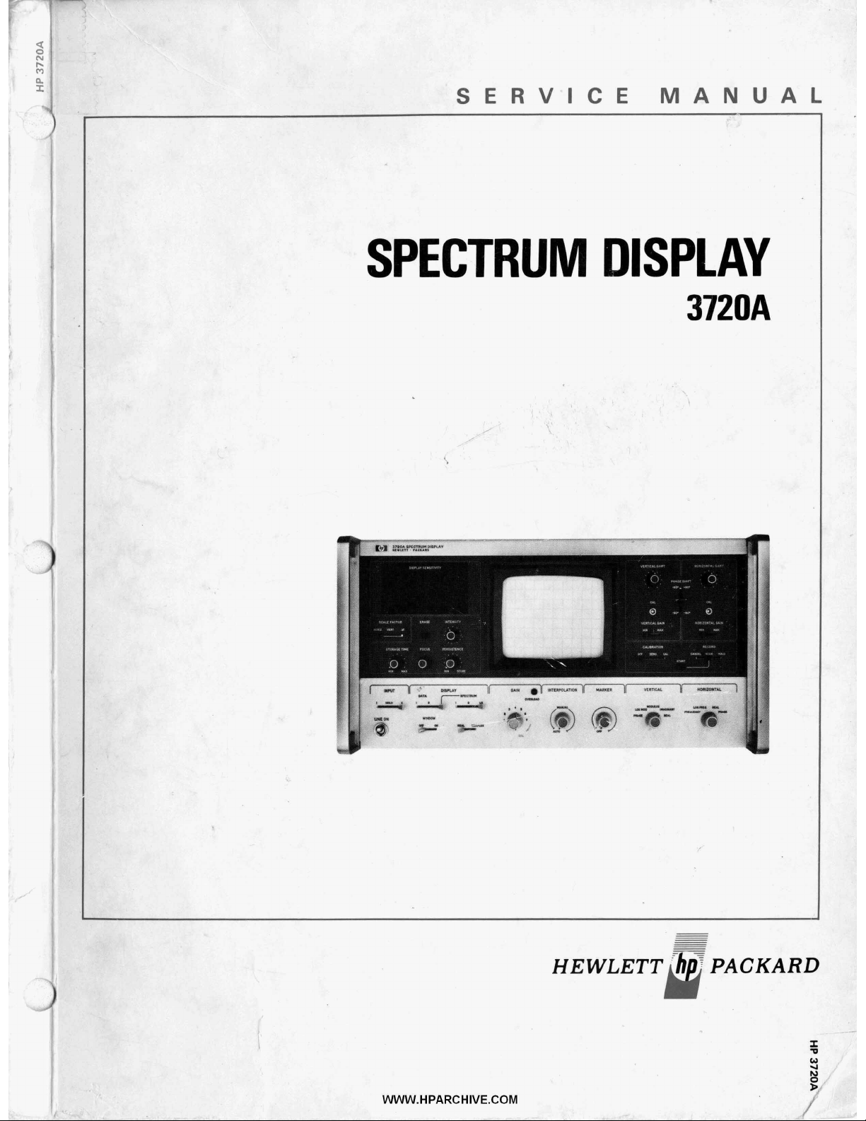
SPECTRUM
DISPLAY
3720A
i’
WWW.HPARCHIVE.COM
*-
Page 3
-
-
-
-
HEWLETT
'TPACKARD
u
SERVICE
MODEL
I-
J
.
SPECTRUM DISPLAY
MANUAL
3720A
SERIAL PREFIX
This manual applies to
1209U. Instruments with
have
a
Manual Change Sheet, to which reference should be
WWW.HPARCHIVE.COM
For
Copyright HEW LETT-PAC
SOUTH QUEENSFERRY, WEST LOTHIAN, SCOTLAND
Free
all
instruments having serial prefix
a
serial prefix above 1209U
made.
Distribution
Only
KAR
D
LIMITED 1972
may
,.
03720-95001
WWW.HPARCHIVE.COM
Printed: APRIL 1972
I
Page 4
Foreword
FOREWORD
For convenience and
ease
of use, information on Model 3720A Spectrum Display
has been presented in two publications:
hp
.OPERATING MANUAL
Part Number 03720-95000
(Microfiche 03720-95025)
hp
.SERVICE MANUAL
Part Number 03720-95001
(Microfiche 03720-95026)
HOW TO ORDER
To order the above publications contact the nearest Hewlett-Packard Sales and
Service Office (addresses
at
the rear of this manual). Give the
hp
Part Number of
the publication and the complete model number, name and serial number of the instrument.
SERVICE MANUAL CONTENT
contains General Servicing Instructions and a Description of Controls
Section
I
and Indicators.
I
Section
gives information on Parts Identification, Maintenance and Repair
Procedu res.
II
Section
Section
Section
contains a list of Replaceable Parts for the 3720A.
V
gives the 3721A/3720A System Troubleshooting Procedure.
V contains the Functional Diagram, Assembly Location Diagrams and
Assembly Packages including Schematic and Component Location.
MICROFICHE
rhese publications are also available in 6in x 4in microfiche form. Each sheet contains
up to 60 pages, maximum, of
text
and illustrations. Order
as
above, quoting the
appropriate hpmicrofiche part number.
ii
WWW.HPARCHIVE.COM
Page 5
LIST
SECTION
OF
CONTENTS
I
INTRODUCTION
List of Contents
Paragraph 1 . 1
1-3
Table
Figure
1-1
1-1
1-2
1-3
Paragraph 2-1
2-3
2-1 5
2-19
2-33
OPERATING INSTRUCTIONS
GENERAL SERVICING INSTRUCTIONS
Accessories furnished with 3720A
Model 3720A Spectrum Display
Front panel controls and indicators
Rear panel controls and connectors
SECTION
INTRODUCTION
IDENTIFICATION
II
GENERAL MAINTENANCE
.........
.........
2-4 Assembly Identification
2-6 Assembly Connection Identification
2-8 Integrated Circuit Identification
INSTRUMENT DlSMANTLl
2-16 Removing Top and Bottom Covers
2-1 7 Removing Side Covers
2-1 8 Front Panel Access
............
.......
..............
..........
..
.........
...
NG
............
...........
.............
....
...
..
....
........
........
MAINTENANCE
2-20 Locations
2-23 Replacement of Display Sensitivity Lamps
2-27 Cleaning the Air Filter
2-29 Cathode Ray Tube RemovaI/RepIacement
2-30 Line Transformer Removal/Replacement
of
dc Power Supply Fuses
..............
.......
...
..............
................
2-31 Chassis Mounted Transistors Plate Removal/Replacement
2-32 High Voltage Tripler Assembly Removal/Replacement
REPAIR PROCEDURES
2-34 Etched Circuits
............................
.......................
2-36 Integrated Circuit Removal/Replacement
...
...
....
....
..
Page
....
..
Page
......
...
...
...
...
...
...
...
...
...
...
...
...
...
...
1-1
1-1
1-1
1-0
1-2
1-4
2-1
2-1
2-1
2-1
2- 1
2-2
2-2
2-2
2-3.
2-3
2-3
2-4
2-4
2-5
2-5
2-5
2-5
2-5
2-6
Table
2- 1
2-2
F
igu re 2- 1
2-2
Paragraph 3- 1
3-3
3-7
WWW.HPARCHIVE.COM
3720A Assem bl ies
Digital integrated circuit abbreviations
..............
....
A18/A19 Housing assembly retaining screws
CRT neck connections
SECTION
I
NT
R 0 DUCT
I 0 N
ORDERING INFORMATION
REFERENCE DESIGNATORS
................
111
REPLACEABLE PARTS
..........
..
..
...
2-1
2-2
..
....
.....
...
...
Page
..
2-3
2-4
3-1
3-1
3-1
...
Ill
Page 6

Model 3720A
3- 8
3-9
iable
Figure
Paragraph 4-1
33- 2
3-
4-3
4-8
4-12
4-14
4-16
4-
1
4-2
4-23
4-25
4-27
LIST OF ABBREVIATIONS
COLOUR ABBREVIATIONS
Replaceable Parts
1
Code List of Manufacturers
Location of cabinet components
1
SECTION
INTRODUCTION
USING TROUBLESHOOTING SECTION
TEST EQUIPMENT
4-10 Logic Probe
SYSTEM TROUBLESHOOTING CONTROLS SET-UP
FLOW A
FLOW B
FLOW
9
FLOW D . Other Transferred Signals Faults
1
FLOW D(a)
FLOW D(b) . Gain Correction Factors Transfer Faults
FLOW D(c)
.
Control Faults
.
Display Sensitivity Faults
C . Data Transfer Faults
.
.
..........
IV
SYSTEM TROUBLESHOOTING
....................
..........................
.............................
Timescale Transfer Faults
Signal Recovery Transfer Faults
..
..
.....
..
......................
............
........
,.
..
........
............
......
........
........
..
...
..
..
..
Page
....
..
..
..
..
..
..
..
..
..
..
3-4
3-50
3-49
4-1
4-1
4-2
4-2
4-3
4-5
4-6
4-7
4-8
4-8
4-9
4-10
P
c
k
I
rable 4- 1
4-
2
4-3
4-4
4-5
4-6
4-7
4-8
Figure
Paragraph 5-1
4- 1
4-2
4-3
4-'4
4-5
5-3
5-5
5-9
Flow charts
3721A/3720A System repair procedure
Test equipment required for System Troubleshooting
Range transfer check
Range data logic check
Ti mescale transfer check
Gain correction factors check
Signal recovery transfer check
750KHz
Transfer Data duration
Data Ready
Transfer Data repetition rate
Multiplexed range outputs
SECTION V SCHEMATICS. COMPONENT LOCATIONS. DIAGRAMS
INTRODUCTION
DRAWING SYMBOLS
ASSEMBLY PACKAGES
5-7 Locating Assembly Packages
THEORY OF OPERATION
5-10 Functional Diagram
..................................
............
..........................
....
..............
..........
..
..................
......
..............
..
..
.....
...........
............
.......
..
...
...
....
..
....
.....
.....
..
4-1
..
4-1
..
4-2
..
4-6
..
4-6
..
4-9
..
4-10
..
4-10
..
4-4
..
4-4
..
4-4
..
4-4
4-6
Page 5-1
5-1
5-1
..
5-1
..
5-1
..
5-1
9
c
Y
I
Figure
5-1 Guide to schematics
5-2 Logic package outlines
WWW.HPARCHIVE.COM
..
..
..
5-2
5-3
1'
i
Page 7

List of Contents
5-3
5-4
5- 5
5-6
5-7
5-8
5-9
Functional diagram
Guide to logic symbols
Location of components (front and rear panels)
Location of assemblies and chassis mounted components (top view)
Location of assemblies and chassis mounted components (underside view)
of
Wiring
rotary switches
Wiring of rear panel connectors
..
.. ..
A1 Not Assigned
A2 Mantissa Range Assembly Package
Figure A2-1 Component location, A2
A2-2 Schematic A2 (part
A2-3
Schematic A2 (part 21, Mantissa Range assembly
1
),
A3 Decade Range Assembly Package
Figure A3-1 Component location, A3
A3-2 Schematic A3, Decade Range assembly
..
.. ..
..
.. .. .. ..
..
..
..
.. ..
.. ..
.. ..
..
..
..
..
..
..
..
..
..
.. .. ..
.. ..
..
.. ..
Mantissa Range assembly
.
. . . . .
. . . . . .
..
..
.. ..
.. .. .
..
..
..
..
..
..
.. ..
..
.. ..
.
.
. .
.
..
..
.
.
..
.. .. ..
..
..
..
..
..
.. ..
.
. . . . . . .
.
. .
. . . . .
..
..
..
.. ..
.
.
.. ..
..
..
..
..
..
..
..
Page
.
..
.
Page
. .. ..
..
5-4
5-4
5-5
5-6
5-7
5-61
5-63
5-10
5-11
5-13
5-14
5-15
A4 Store 1 Assembly Package
Table A4-1 Component identification grid, A4
Figure
A4-1 Component location, A4
..
.. .. .. ..
A4-2 Schematic A4 (part 11, Store 1 assembly
A4-3 Schematic A4 (part 21, Store 1 assembly
A5 Store 2 Assembly Package
Figure A5-1 Component location, A5
45-2 Schematic A5, Store 2 assembly
..
.. ..
..
._
A6 Buffer Assembly Package
Figure
.
A6-1 Component location, A6
A6-2 Schematic A6, Buffer assembly
..
..
.. ..
._
A7 Switch Card Assembly Package
Table A7-1 Component identification grid, A7
F igu re A7-1 Component location, A7
..
..
..
..
A7-2 Schematic A7, Switch Card assembly
._
.
Page
517
..
.,
..
..
_. ..
.
.
.
.
.
..
..
5-16
_.
5-17
..
5-19
Page
5-20
..
..
5-21
Page
5-22
__
__
5-23
Page
5-25
..
524
..
5-25
A8 Hybrid Multiplier Assembly Package
Table A8-1 Component identification grid, A8
Figure
A8-1 Component location, A8
..
.. .. ..
A8-2 Schematic A8, Hybrid Multiplier assembly
WWW.HPARCHIVE.COM
..
._
.
..
..
._
..
..
..
Page
5-27
_.
5-26
..
527
,
Page 8
Model 3720A
A9 Window Multiplier Assembly Package
Table A9-1 Component identification grid, A9
.
, . ._
..
..
Page 5-29
F
igu re
A9-1 Component location, A9
A9-2 Schematic A9, Window Multiplier assembly
...............
..
A10 Integrator Assembly Package
Table A10-1 Component identification grid, A10
Figure
A10-1 Component location, A10
..........
A10-2 Schematic A10, Integrator assembly
.. ..
..
A1 1 Polar Converter Assembly Package
Table A1 1-1 Component identification grid, A1
F igu
re
A1 1-1 Component location, A1 1
A1 1-2 Schematic A1 1, Polar Converter assembly
A1 2 Low Voltage Power
Supply
Assembly Package
Table A12-1 Component identification grid, A12
1
............
....
..........
Figure A12-1 Component location, Chassis Mounted Transistors
A12-2 Schematic, Line Module and Line Transformer
A12-3 Component location, A12
.......................
..........
A1 2-4 Schematic A1 2, Low Voltage Power Supply assembly
........
.
........
........
........
........
...
....
....
Page
....
....
Page 5-33
....
.
..
Page
....
....
_.
._
.
5-28
529
5-31
5-30
5-31
532
5-33
5-37
5-34
5-35
5-36
5-37
1
A1 3 Control Logic Assembly Package
Table A13-1 Component identification grid, A13
Figure
A13-1 Component location, A13
A13-2 Schematic A13 (part
11,
....................
Control Logic assembly
A13-3 Schematic A13 (part 2), Control Logic assembly
A14 Triangle Wave Generator Assembly Package
Table A14-1 Component identification grid, A14
Figure
A14-1 Component location, A14
A14-2 Schematic A14 (part
11,
A14-3 Schematic A14 (part 2), Triangle
............................
Triangle
Wave
Wave
A15 Sine Shaper Assembly Package
Table A15-1 Component identification grid, A15
Figure
A151 Component location, A15
A1 5-2 Schematic A1 5 (part
11,
...............
Sine Shaper assembly
A15-3 Schematic A15 (part 21, Sine Shaper assembly
.. ..
..
..
..
Generator assembly
Generator assembly
..
..
..
..
..
..
Page
..
_.
....
....
Page
....
....
....
Page
....
....
,.
5-39
5-38
5-39
541
5-43
542
5-43
5-45
5-47
5-46
5-47
5-49
r
.
vi
WWW.HPARCHIVE.COM
Page 9
List of Contents
A16 Deflection Amplifiers Assembly Package
.
Page
Table A16-1 Component identification grid, A16
F igu re
1
A16-1 Component location, A16
A16-2 Schematic A16 (part
l),
A16-3 Schematic A16 (part 21, Deflection Amplifiers assembly
..
.. .. ..
..
..
..
..
_.
.. .. ..
Deflection Amplifiers assembly
..
5-51
..
5-50
..
5-51
-
..
5-53
I
i
A1 7 High Voltage Power Supply Assembly Package
Table A17-1 Component identification grid, A17
Figure
A17-1 Component location, A17
..
.. ..
A17-2 Schematic A17, High Voltage Power Supply assembly
A1
8
Range Indicator Assembly
Table A18-1 LED Truth Table
Figure
A18-1 Component location, A18
_.
..
_. .. .. .. .. _.
A18-2 Schematic A18, Range Indicator assembly
A19 Range Units Assembly Package
Figure A19-1 Component location, A19
.. ..
.. .. ..
A19-2 Schematic A19, Range Units assembly
.. ..
..
.
..
..
Page
5-55
. ..
..
..
Page
,
..
..
Page
..
..
554
5-55
5-57
5-56
5-57
556
5-57
..
..
..
..
..
..
..
..
..
..
..
.
,.
A20 Storage Assembly Package
._ ..
Page
.. ..
,
..
5-59
5-58
5-59
Table A20-1 Component identification grid, A20
Figure A20-1 Component location, A20
..
..
.;
A20-2 Schematic A20,Storage assembly
..
. . .
. . . .
..
.
.
..
>
vii
WWW.HPARCHIVE.COM
Page 10
--
Model
3720A
t
L
1-0
WWW.HPARCHIVE.COM
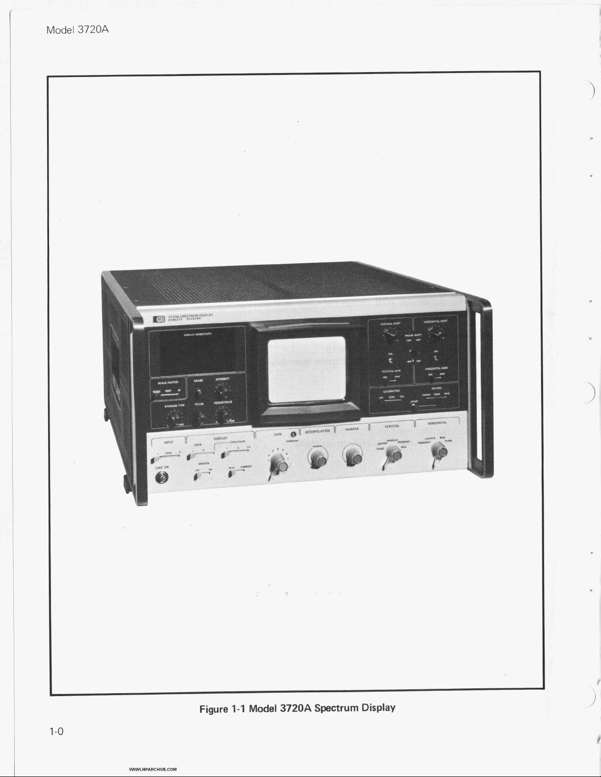
Figure
1-1
Model
3720A
Spectrum Display
Page 11
Section
I
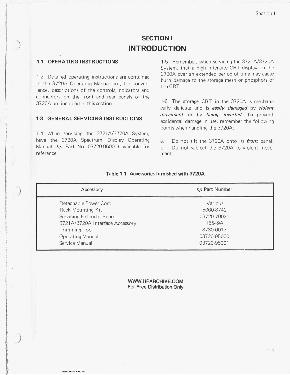
SECTION
I
INTRODUCTION
1-1
OPERATING INSTRUCTIONS
1-2 Detailed operating instructions are contained
in the 3720A Operating Manual but, for convenience, descriptions of the controls, indicators and
connectors on the front and rear panels of the
3720A are included in this section.
1-3
GENERAL SERVICING INSTRUCTIONS
1-4 When servicing the 3721A/3720A System,
1
Table
1-1
Accessories furnished with 3720A
1-5 Remember, when servicing the 3721A/3720A
a
System, that
3720A over an extended period of time may cause
burn damage
theCRT,
1-6
The storage CRT in the 3720A is mechani-
cally delicate and
movement
accidental damage in use, remember the following
points when handling the 3720A:
high intensity CRT display on the
to
the storage mesh or phosphors of
is
or by
easily damaged
being inverted.
by
To prevent
violent
3
hp
Part
Accessory
Detachable Power Cord Various
Rack Mounting
Servicing Extender Board 03720-70021
3721 A/3720A Interface Accessory 15549A
Trimming
Operating Manual 037 20-95000
Service Manual 03720-9500
Tool
Kit
WWW.HPARCHIVE.COM
For
Free
Distribution
Only
Number
5060-8742
8730-001 3
1
WWW.HPARCHIVE.COM
1-1
Page 12

Model
3720A
10
3
4
5
6
7
8
9
1'1
1'2
2
1
27 26 25
28
29
30
L
31
24
23
22
13
14
1'5
16
ii
is
21
1-2
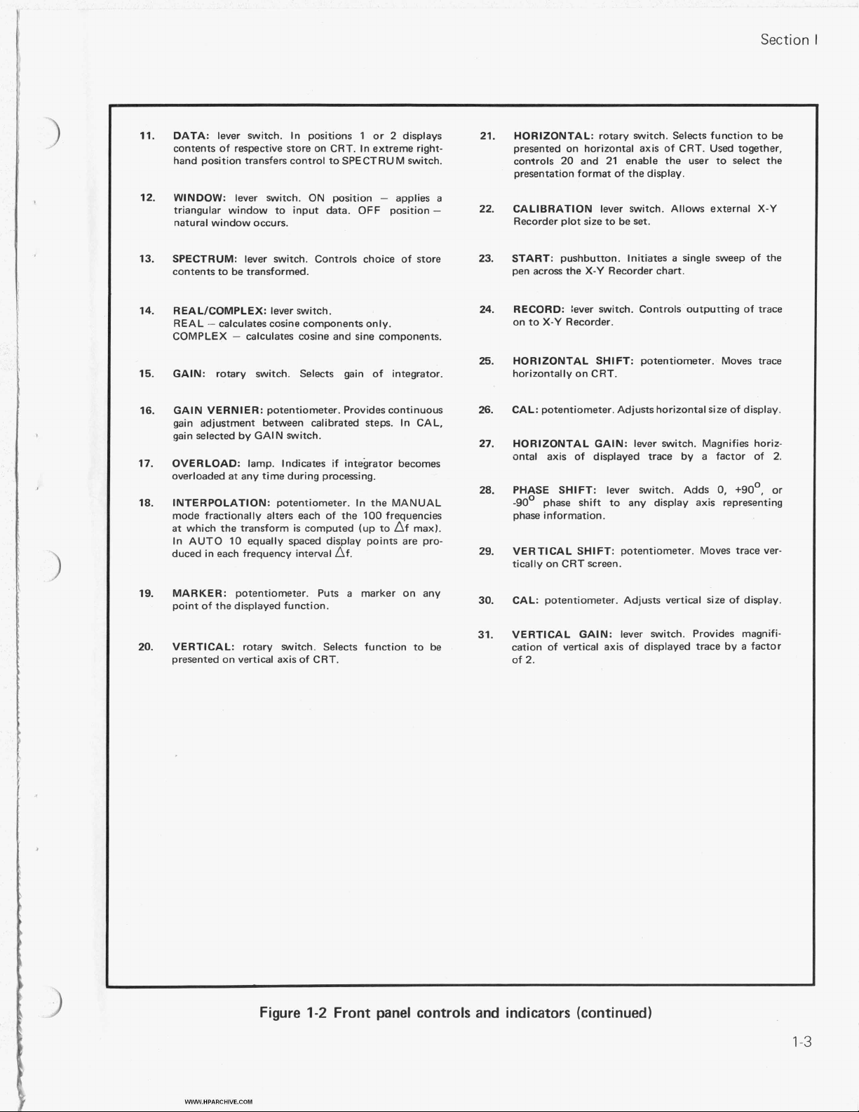
DISPLAY:
1.
calibrated
brated
DISPLAY SENSITIVITY:
2.
Scales the horizontal and vertical axes and the fre-
quency ..interval,
switch.
SCALE FACTOR:
3.
tion to be presented on the Display Sensitivity panel.
ERASE:
4.
on storage CRT screen, when not
INTENSITY:
5.
CRT
8
y
10 division CRT, with graticule
in
one division squares. Major axes cali-
in
0.2
division intervals. 1 division = 0.95cm.
illuminated digital readout.
Af,
as selected by Scale Factor
lever switch. Selects axis calibra-
pushbutton. Eradicates all traces displayed
potentiometer. Controls brightness of
beam.
Figure
in
1-2
STORAGE TIME:
6.
any display is stored, when
STORE mode.
FOCUS:
7.
beam.
PERSISTENCE:
8.
written trace, when not
clockwise position selects STORE mode.
INPUT:
9.
into Store 1 or
data
LINE-ON:
10.
instrument.
potentiometer. Adjusts sharpness of CRT
lever switch. Routes data from the 3721A
in
stores.
toggle switch. Controls ac supply to
Front panel controls and indicators
potentiometer. Varies the time
in
STORE mode.
potentiometer. Controls duration of
2
as selected.
in
STORE mode. Fully
In
HOLD
position retains
the
WWW.HPARCHIVE.COM
Page 13
Section
I
DATA:
11.
contents of respective store on CRT. In extreme righthand position transfers control to SPECTRUM switch.
12.
WINDOW:
triangular window to input data.
natural window occurs.
13. SPECTRUM:
contents to
14. REAL/COMPLEX:
REAL
COMPLEX
15.
GAIN:
GAIN VERNIER:
16.
I
gain adjustment between calibrated steps. In CAL,
gain selected by GAIN switch.
OVERLOAD:
17.
overloaded at any time during processing.
18. INTERPOLATION:
mode fractionally alters each of the
at
In AUTO
duced in each frequency interval df.
lever switch. In positions 1 or 2 displays
lever switch. ON position - applies a
OFF
lever switch. Controls choice of store
be
transformed.
-
calculates cosine components only.
rotary switch. Selects gain of integrator.
which the transform
lever switch.
-
calculates cosine and sine components.
potentiometer. Provides continuous
lamp. Indicates
potentiometer. In the MANUAL
10
equally spaced display points are pro-
if
integrator becomes
is
computed (up to Af max).
100
position
frequencies
21. HORIZONTAL:
presented on horizontal axis of CRT. Used together,
controls
presentation format of the display.
22.
-
CALIBRATION
Recorder plot size to be set.
23.
START:
pen across the X-Y Recorder chart.
RECORD:
24.
on to X-Y Recorder.
HORIZONTAL SHIFT:
25.
horizontally on CRT.
CAL:
26.
27.
28.
29.
potentiometer. Adjusts horizontal size of display.
HORIZONTAL GAIN:
mtal axis of displayed trace by a factor of
PHASE SHIFT:
-90'
phase shift to any display axis representing
phase information.
VERTICAL SHIFT:
tically on CRT screen.
rotary switch. Selects function to be
20
and
21
enable the user to select the
lever switch. Allows external X-Y
pushbutton. Initiates a single sweep of the
Lever switch. Controls outputting of trace
potentiometer. Moves trace
lever switch. Magnifies horiz-
lever switch. Adds
potentiometer. Moves trace ver-
0.
+goo,
2.
or
19. MARKER:
point of the displayed function.
VERTICAL:
20.
presented on vertical axis of CRT.
potentiometer. Puts a marker on any
rotary switch. Selects function to
be
30. CAL:
31.
potentiometer. Adjusts vertical
VERTICAL GAIN:
cation of vertical axis of displayed trace by a factor
of
2.
lever switch. Provides magnifi-
size
of display.
3
WWW.HPARCHIVE.COM
Figure
1-2
Front panel controls and indicators (continued)
1-3
Page 14
Model
3720A
1
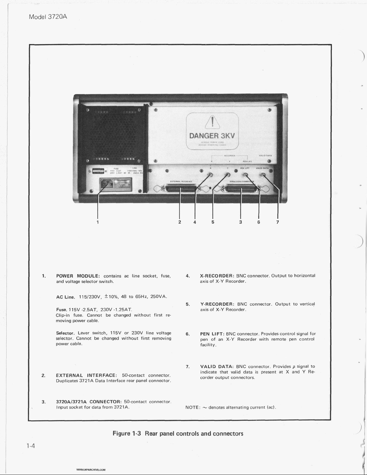
1.
POWER MODULE:
and voltage selector switch.
AC
Line.
11 51230V. k 10%.
Fuse.
115V -2.5AT, 230V -1.25AT.
Clipin fuse. Cannot be changed without first
moving power cable.
Selector. Lever switch, 115V
selector. Cannot
power cable.
2.
EXTERNAL INTERFACE:
Duplicates 3721A Data Interface rear panel connector.
contains ac line socket, fuse,
48
to 65Hz. 250VA.
or
be
changed without
230V line voltage
50-contact connector.
first
re-
removing
24
4.
5.
6.
5
X-RECORDER:
axis of
Y-RECORDER:
axis of
PEN LIFT:
pen of an
facility.
VALID DATA:
indicate that valid data is present at
corder output connectors.
3
X-Y
X-Y
BNC connector. Output to horizontal
Recorder.
BNC connector. Output to vertical
Recorder.
BNC connector. Provides control signal for
X-Y
Recorder with remote pen control
BNC connector. Provides p signal to
6
7
X
and
c
Y
Re-
3. 3720A13721A CONNECTOR:
Input
socket for data from 3721A.
1-4
WWW.HPARCHIVE.COM
50-contact connector.
Figure
1-3
-
NOTE:
denotes alternating current (ad.
Rear panel controls and connectors
Page 15
L
_.
..
.
SECTION
GENERAL MAINTENANCE
2-1
INTRODUCTION
2-2 This section contains information on Identification, Instrument Dismantling and Repair Procedures for the 3720A.
2-3 IDENTIFICATION
2-4
Assembly Identification
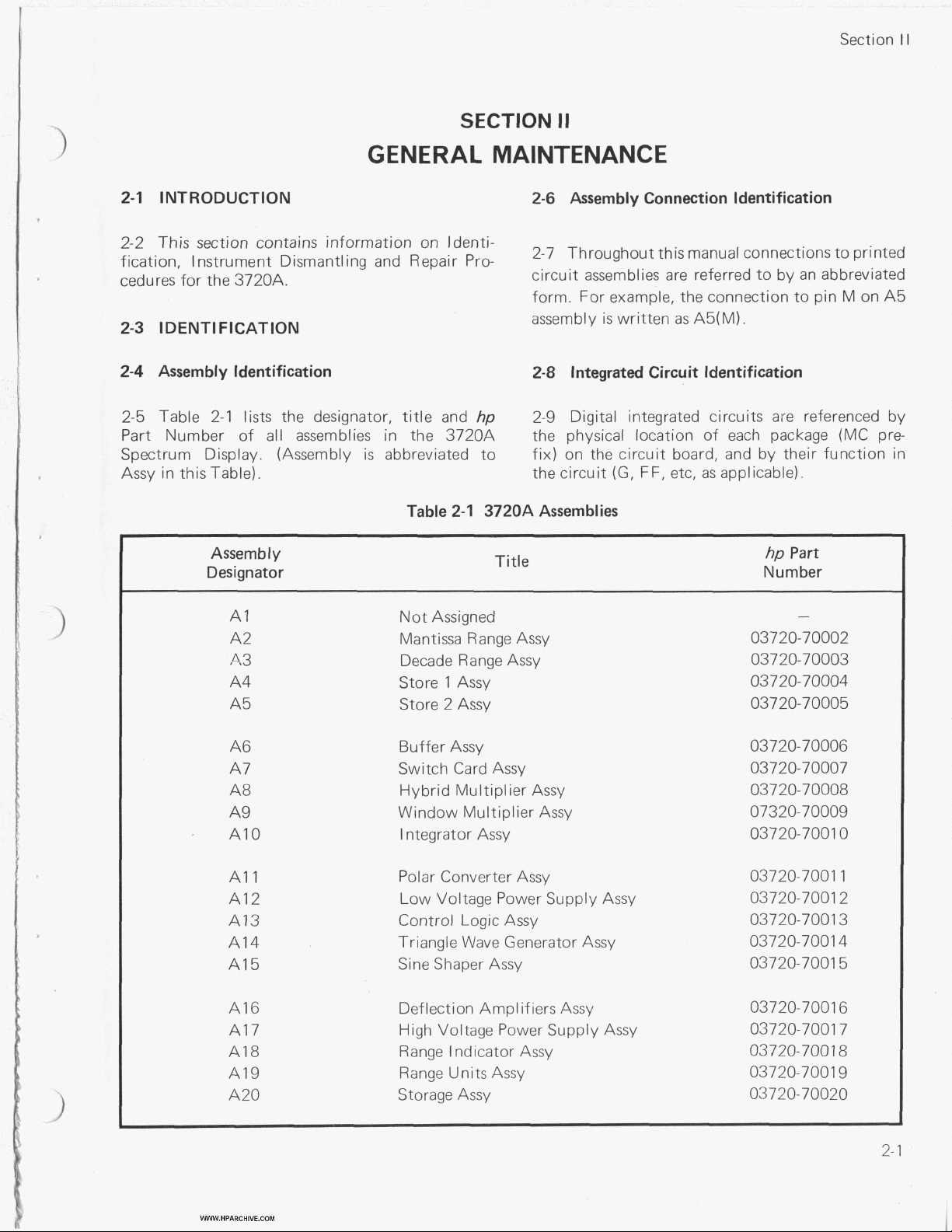
2-5 Table 2-1 lists the designator,
Part Number
of
all assemblies in the 3720A
Spectrum Display. (Assembly
Assy in this Table).
title
and
is
abbreviated to
hp
Section
II
2-6 Assembly Connection Identification
2-7 Throughout this manual connections to printed
circuit assemblies are referred to by an abbreviated
form. For example, the connection to pin M on A5
assembly is written
2-8
Integrated Circuit Identification
2-9 Digital integrated circuits are referenced by
the physical location of each package (MC prefix) on the circuit board, and by their function in
the circuit
(G,
as
FF, etc,
A5(M).
as
applicable).
II
Assemb
I
y
Designator
A?
A2
4.3
A4
A5
A6
A7
A8
A9
A1
0
A1
1
A12
A13
A14
A1 5
Table 2-1 3720A Assemblies
Title
Not Assigned
Mantissa Range Assy
Decade Range Assy
Store
1
Assy
Store 2 Assy
Buffer Assy
Switch Card Assy
Hybrid Multiplier Assy
Window Multiplier Assy
Integrator Assy
Polar Converter Assy
Low Voltage Power Supply Assy
Control Logic
Triangle
Assy
Wave
Generator Assy
Sine Shaper Assy
hp
Part
Number
-
03720-70002
03720-70003
03720- 70004
03720-70005
03720- 70006
03720-70007
03720-70008
07320-70009
03720-7001
0
03720-7001
03720-7001 2
03720-7001 3
03720-7001 4
03720-7001 5
1
A16
A1 7
A1
8
A1 9
A20
WWW.HPARCHIVE.COM
Deflection Amplifiers Assy
High Voltage Power Supply Assy
Range Indicator Assy
Range Units Assy
Storage Assy
03720-7001 6
03720-7001 7
03720-7001
8
03720-7001 9
03720- 70020
2-1
Page 16
Model
3720A
.2-10 The MC number gives the physical location of
each package in the form of
2-11 With the printed circuit board held component side uppermost, and tongued connector near-
est,
numbering of the rows and columns of inte
grated circuits starts from the top left hand corner
of the board. The first figure following the MC
prefix
column. For example, MC52 will
row down and the 2nd column across, whilst
MC103 will be in the 10th row and 3rd column.
2-1 2 The second method
individual 'component blocks' helps the circuit
description and signal flow indication.
2-13 Each 'block'
its function
number indicating
diagram, in the same manner
etc, are referenced.
gives
the row and the second gives the
of
is
given a prefix according to
(see Table 2-2 for
its
position on the schematic
a
grid reference.
lie
in the 5th
identification of the
full
list) and
a
as
resistors, capacitors,
a
2-15 INSTRUMENT DISMANTLING
I
115/230V AC AND +158V DC SUPPLY
WIRES ARE EXPOSED WHEN ANY
THE INSTRUMENT COVERS ARE
MOVED. USE EXTREME CAUTION DURING TROUBLESHOOTING, ADJUSTMENT
OR
REPAIR. AVOID DAMAGE TO THE
INSTRUMENT BY DISCONNECTING THE
POWER CABLE BEFORE REMOVING
REPLACING COVERS, ASSEMBLIES
COMPONENTS.
2-16 Removing Top and Bottom Covers
1.
Remove the four cross-head screws holding the
cover in position.
2. Slide the cover about lin (2.5cm) to the rear
and lift clear.
NOTE:
the tilt stand from the bottom cover before
rem ova
It is not necessary to remove the feet
I.
DANGER
OF
RE-
OR
OR
or
c
Table 2-2 Digital integrated circuit abbreviations
I
Abbreviation
B
DD
FF
G
IG
MS
SR
IC
2-14 All
assembly connections. For example, lead 12 on
integrated circuit MC25, on A5 assembly, is
referred to
scribing schematics, lead
assembly A2 would be referenced A2FF9(6).
leads are referred to in the same way
as
A5MC25(12). Similarly when de-
F
unction
Buffer
Decade Divider
FI ip-f lop
Gate
Inverter Gate
Monostable
S
h if t Register
6
on Flip-flop 9 on
as
2-1 7 Removing Side Covers
1. Remove the four cross-head screws securing
each cover.
2. Lift cover clear.
2-18 Front Panel Access
1.
Remove the
instru ment.
Release the two screws securing the Al/All
2.
retaining strip and lift this strip clear.
3.
Remove assemblies A2 to A1
4.
Release the two screws
of the right hand and left hand board guides.
Withdraw the board guides to
5.
the rear
Re-assembly is
6.
cedu re.
top
and
of
the front panel.
a
reversal of the above pro-
bottom
at
covers from the
1
inclusive.
the base of each
give
access
to
2-
2
WWW.HPARCHIVE.COM
Page 17

Section
II
2-19 MAINTENANCE
CAUTION
When handling the 3720A do not
instrument onto
2-20 Locations
2-21 Access
-22V and -5OV power supply fuses
removing the
2-22 The +12.6V power supply fuse
Storage assembly. Access to the fuse
removing the
2-23 Replacement
to
its
front panel.
of
dc Power Supply Fuses
the +158V, +50V, +15V, +5V,
bottom
top
cover of the 3720A.
cover of the instrument.
of
Display Sensitivity Lamps
tilt
is
gained by
is
on the A20
is
gained by
the
-1
5V,
Remove the four nuts holding the A18/A19
6.
housing assembly to the front panel. If
necessary, gently move the wiring to gain
access
Release screw
7.
8.
Holding the A18/A19 housing assembly with
one hand, gently press the Display Sensi-
tivity panel on the front of the instrument
with the other hand to release the assembly.
Replacement
9.
bly
to the nuts.
B
shown in Figure 2-1.
of
the A1 8/A19 housing assem-
is
a
reversal of the above procedure.
3
.3
2-24 The lamps are mounted on the A18 and A19
assemblies.
housing assembly must be removed from the
instrument and then dismantled.
2-25 Removal
1.
Remove the
fluted aluminium plate from the instrument.
Note that the fluted aluminium plate
adhesive.
2.
Release the two screws securing the Al/All
retaining strip and
3.
Remove assemblies A2 to A6 inclusive.
4.
Release the two screws
left hand board guide and withdraw the
board guide.
Remove the left hand board guide support
5.
by releasing the three screws A shown in
Figure 2-1.
To
replace the lamps the A18/A19
of
A18/A19 Housing Assembly
top
cover,
left
side cover and
lift
this strip clear.
at
the base
is
of
self-
the
(
Figure 2-1 A18/A19 Housing assembly
retaining screws
2-26 Dismantling the A18/A19 Assembly
1.
Remove the A18/A19 housing assembly
detailed in Paragraph 2-25.
2.
Release
units lamp separator in place.
3.
Slide
I
If
the separator
lamps will be damaged.
the two screws holding the range
the separator away from the assembly.
CAUTION
is
forced sideways the units
103720
xOO56j
as
WWW.HPARCHIVE.COM
2-3
Page 18

Model 372QA
as
4. Pull out A18 and/or A19 assemblies
quired and disconnect the A18/A19 interconnecting cables.
5. Renew the faulty lamps.
6.
Re-assembly is a reversal of the above pro-
cedu re.
2-27
Cleaning The Air Filter
2-28 The air filter on the fan cover of the 3720A
should be removed periodically for cleaning. Four
screws secure the fan cover to the back panel.
2-29
Cathode Ray Tube Removal/Replacement
DANGER
re
12. Remove the black light shield surrounding
the CRT screen by gently squeezing it
top centre and bottom centre and pulling
clear.
13. Unscrew and remove the bezel.
14. Slacken theclamp on the rear of the CRT neck.
15. Holding the screen
gently press the rear of the tube with the
other hand and slide the CRT forward and
out.
NOTE: To prevent accidental damage to the
storage mesh
DO
WNWA R
16. Re-assembly
cedure.
DO
DS.
is
of
CRT with one hand,
NOT TILT THE CRT FACE
a
reversal of the above pro-
at
the
WHEN HANDLING THE CRT ALWAYS
WEAR GOGGLES AND GLOVES. HANDLE
WITH EXTREME CARE.
Disconnect the power cable from the 3720A
1.
top
Remove the
2.
Remove the back panel high voltage cover.
3.
Unplug the CRT socket.
4.
Release the two screws holding A20 in
5.
place and
Unplug the wires connected to the neck
6.
of the CRT. The colours of the wires are
shown in Figure 2-2.
Remove AZO support block by releasing
7.
the two screws which hold
Release
8.
retaining strip and lift this strip clear.
Remove assemblies A2 to A6 inclusive.
9.
Remove the two screws holding the high
10.
voltage connector A55J1 in place. Disconnect
the flexible wiring from this connector.
Unplug the wire from the collimator conn-
11.
ector on the side of the CRT.
lift
the two screws securing the Al/All
cover from the instrument.
out A20.
it
in place.
1
A16 DEFLECTION AMPLIFIERS ASSY
cu
CR3
Figure
2-2
CRT neck connections
I
2-4
1
WWW.HPARCHIVE.COM
Page 19
Section
I1
2-30 Line Transformer Removal/Replacement
Tilt the 3720A onto
1.
Remove the
2.
top
and
its
bottom
right hand side.
covers from the
instru ment.
3.
Release
the
two screws holding A20 in place
and lift out A20.
Remove the back panel high voltage cover.
.4.
Remove the internal high voltage cover.
5.
Unplug the five wires from A17 and then
6.
remove
7.
Remove XA20 mounting plate and pull
AI
7.
gently to the side.
Note the wire colours against the corres-
8.
ponding pin numbers on the top and bottom
of the line transformer and then unsolder
the connections.
Remove the four screws holding the trans-
9.
former in position. Retain the underside
nuts and safety mouldings and pull the transformer out through the top of the instrument.
Re-assembly
10.
is a
reversal of the above pro-
cedu re.
2-31 Chassis Mounted Transistors Plate
Removal/Replacement
it
2.
Remove the internal high voltage cover.
3.
Remove the rear panel high voltage cover.
4.
Unplug the five wires from A17 and then
remove A1 7.
Unsolder the black and grey wires from the
5.
ground
6.
Release the two screws holding A20 in place
tag.
and lift out A20.
1.
Remove XA20 mounting plate.
8.
Release
the two screws securing the Al/All
retaining strip and lift this strip clear.
Remove assemblies A2 to A6 inclusive.
9.
Remove A20 support block. Two screws
10:
hold
it
in place.
Remove the two screws holding the high
11.
voltage connector A55J1 in place. Disconnect
the flexible wiring from this connector.
12.
Unsolder the wires from XA(20(L) and
XA20(N) after noting their colours.
13.
Remove the wires from the grommet.
Lift out the high voltage tripler assembly.
14.
15.
Re-assembly
is a
reversal of the above pro-
cedu re.
Remove the
1.
top
cover and
right
side cover
from the instrument.
2.
Release
the
two
screws securing the A12/
A16 retaining strip and lift this strip clear.
Remove assemblies A12 to A16 inclusive.
3.
4.
Release
the two screws
at
the bottom of the
transistor plate.
Withdraw the plate.
5.
6.
Renew the faulty transistors
7.
Re-assembly
is a reversal of the above pro-
as
necessary.
cedu re.
2-32 High Voltage Tripler Assembly Removal/
Replacement
Remove the
1.
WWW.HPARCHIVE.COM
top
cover from the instrument.
2-33 REPAIR PROCEDURES
2-34 Etched Circuits
2-35The etched circuit boards in the Spectrum
Display are of the plated-through type, consisting
of metallic conductors bonded to both sides of the
insulating material. The metallic conductors are
extended through the component mounting holes
by
a
plating process. Solder connection can be
made from either side of the board with equally
good results. Following
are
recommendations and
precautions pertinent to etched circuit repair
work
:
a.
Avoid unnecessary component substitution;
it
can result in damage to the circuit board and/or
adjacent components.
2-5
Page 20
Model 3720A
b. Do'not use
etched circuit boards. Excessive heat may lift
conductor
ing iron
c.
or
is
sufficient.
Use a suction device, eg, Soldapult,
a
high-power soldering iron on
damage the board. A
40
watt solder-
or
wooden
a
toothpick to remove solder from component
mounting holes. Care must
be
i3ken when clearing out component mounting holes; never use
sharp metal objects, such
as
an awl
or a twist-drill,
which could damage the plated-through conductor.
d. After soldering, remove
soldered areas with
e.
When removing a multiple connection com-
ponent, such
it gradually, using
a
as
an integrated circuit, loosen
a
gentle side-to-side motion,
excess
flux from the
soac and water solution.
to avoid damage to the plated-through conductors.
2-36
Integrated Circuit Removal/Replacement
2-37 There are three recommended methods of
removing integrated circuit packages from
a
printed
circuit board:
a.
Solder Gobbler.
Solder
iron with
is
removed from the board by a soldering
a
hollow tip connected to a vacuum
source. This permits an
so
that
it
may be replaced if an error has been
This
is
the best method.
IC
to be removed intact
made in diagnosis.
b.
Desoldering
8690-0060).
vacuum operated Solder Gobbler
Tool.
(Soldapult
This method
-
hp
is
recommended if
is
not available.
Part
No.
Remove the solder from each lead by using the
soldering iron and the desoldering tool together.
c.
Clip
Out.
This is the
three methods. Clip the leads
as
possible.
With a soldering iron and long nose
least
satisfactory of the
as
close to the case
pliers carefully remove the leads from each hole.
a
2-6
WWW.HPARCHIVE.COM
Page 21

Section
I I I
SECTION
111
REPLACEABLE PARTS
3-1
INTRODUCTION
3-2
This section contains information for ordering replaceable parts. Table
numerical order of their reference designators and
a.
Hewlett-Packard stock number.
Description (abbreviations given in Paragraphs
b.
c.
Total quantities
d.
Manufacturer and Manufacturer's part number (Code
1
J
3-3
ORDERING INFORMATION
3-4
To
order a replacement part, address the order or enquiry to your local Hewlett-Packard Sales and
Service Office (addresses are listed
of
each part used in the instrument (refer to TQ column).
at
the rear of this manual).
gives
the following information for each part:
3-7,
3-8
and
3-9).
List
of Manufacturers given in Table
3-1
lists parts in alpha-
3-2).
3-5
Specify the following information for each part:
a.
Model and full serial number of instrument.
b. Hewlett-Packard stock number.
c.
Circuit reference designator.
d. Description.
3-6
To
ocder a part not listed in the tables, give a complete description of
and location in the instrument.
3-7
REFERENCE DESIGNATORS
A
C
CR
DS
F
IC
J'
=
assembly
=
capacitor
=diode
=lamp
=
fuse
=
integrated circuit
=
connector (female)
L
MC
MP
P
0
R
=
inductor
=
micro circuit
=
metal work/
miscellaneous part
=
plug (male)
=
transistor
=
resistor
the
part including
S
SR
T
XA
its
function
-=
switch
=
shift register
=
transformer
=
printed circuit
board edge
connector
WWW.HPARCHIVE.COM
3-
1
Page 22
Model 3720A
3-8
LIST
OF
ABBREVIATIONS
A
AC
AL
AMPL
ASSY
BD
BHD
BKDN
CBL
COAX
COMP
CONCEN
CONN
CONT
CRT
DIO
DPDT
FET
FXD
GE
HV
HS
IC
=
ampere
=
alternating
current
=
aluminium
=
amplifier
=
assembly
=
board
=
bulkhead
=
breakdown
=
cable
=
coaxial
=
compensated
=
concentric
=
connector
=
controlled
=
cathode ray tube
=
diode
=
double pole,
double throw
=
field effect
transistor
=
fixed
=
germanium
=
high voltage
=
high speed
=
integrated
circuit
INCD
IND
INV
I/P
K
=
incandescent
=
inductor
=
invert
=
input
=
kilo
(
lo3)
LED = light emitting diode
LH
LIN
LVR
M
MA
MH
MTG
MW
NAND
=
left hand side
=
linear
=
lever
=
mega
(
1 O6
=
milli ampere
=
milli henry
=
mounting
=
milli watt
=
not and
)
NOR =notor
NPN
=
negative-positivenegative
NSR
OPER
PC
PF
PIV
PNP
=
not separately
rep
I
acea ble
=
operational
=
printed circuit
=
pic0 farad
=
peak inverse volts
=
positive-negative-
(1
O-'*
positive
QUAD = quadruple
REC
RH
=
rectifier
=
right hand
side
RND =round
=
RTRY
SI
SPDT
rotary
=
si I icon
=
single pole,
double throw
SPST
=
single pole,
single throw
SW
T
TEMP
TGL
TQ"
UF
=switch
=
throw
=
temperature
=
toggle
=
total quantity
=
micro farad
(10-6)
V
=
volt
VAR = variable
W
WVDC
XFMR
=
watt
=
working voltage
d i rec
t
cu r re n
=
transformer
XR =expander
XSTR
=
transistor
t
3-9
COLOUR ABBREVIATIONS
BLK
BRN
RED
ORN
2
3-
=
black
=
brown
=
red
(2)
=
orange (3)
WWW.HPARCHIVE.COM
(0)
(1
)
'except for those components with#TQ after the description. In
cases
these
the number after#
multiply the number in the total quantity column by
TQ
for true quantity.
=
YEL
GRN
BLU
VI0
yellow
=
green
=
blue
=
violet
(4)
(5)
(6)
(7)
GRY
=
grey
WHT =white
SI
LV
=
silver
(8)
(9)
Page 23

Table
3-1
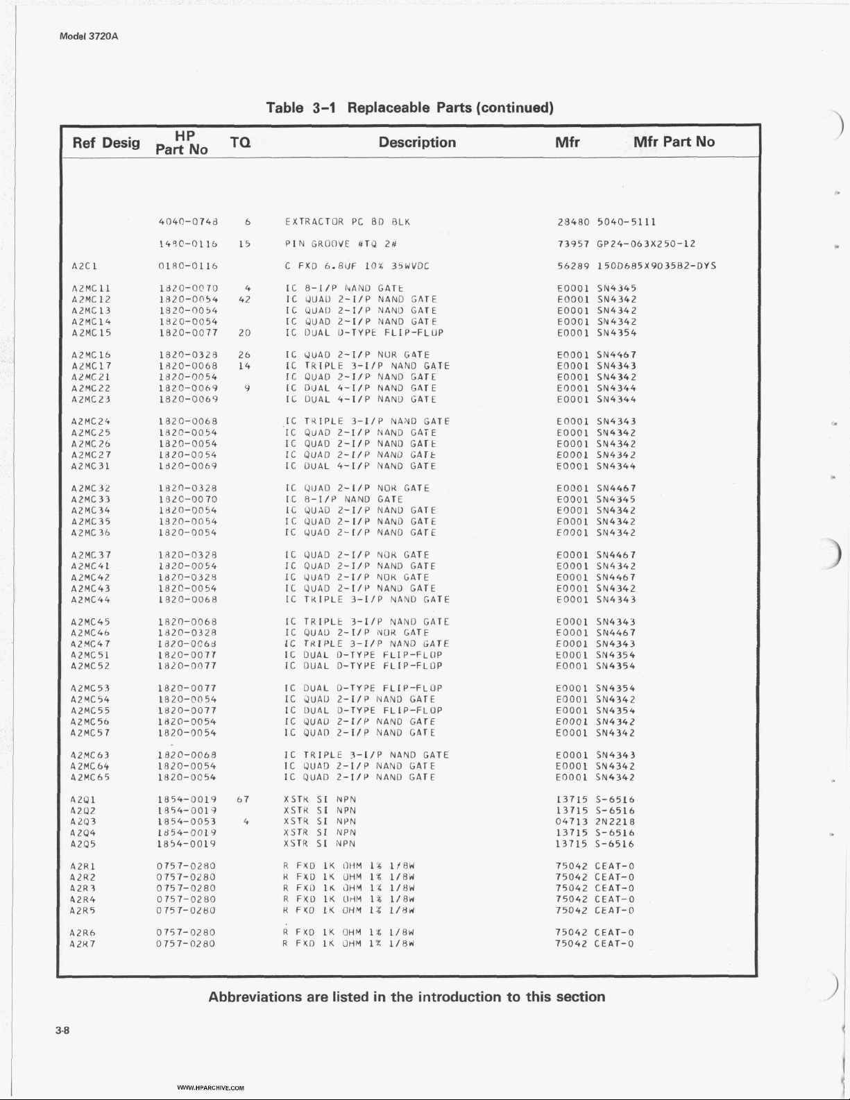
Replaceable Parts
Ref
A1
A2
A3
A4
A5
A6
A7
A8
A9
A10
All
A12
A13
A14
A15
A16
A17
A18
A19
A20
A41
442
A43
A
44
a45
446
44
7
A48
A49
4
50
451
PartNo
8120-1351
8120-
812
8
120- 1369
0 3 72
03720-95001
03
720-7002
5060-8742
155496,
921
9220-1546
9220-1551
9220-1547
9
22
9220-1549
03
72
03720-70003
03
72
0372
03720-70006
0
3720-
03720-70008
03720-70009
03720-700
03
72
0372
0
3 72
03720-
03720-70015
03720-
j
0372003720-7001 8
03720-70019
03720-70020
0372
03720-70042
03720-
03720-70044
03
720-
03720-70046
03720-70047
0372
03720-70049
03720-70050
03720-7005
HP
1348
0-
1689
0-9 5 0 0 0'
1-1356
2-0
32 5
0-
70002
0-
70
004
0-70005
70007
LO
0-
700
1
0-7001
0-
700
1
7001
70016
7001
0-7004
70043
7004
0-
70046
TO Description Mf r Mfr Part
ACCESSORIES
1
2
3
4
7
1
5
1
CABLE POrJER DETACHABLE #UK#
HANUAL OPERATING
MANUAL SFRVICE
1
BOAHD EXTENDER SERVICING
KIT RACK MOUNTING
ACC€SSURY 3721A/3720A INTERFACE
PACKING MATtRIALS
CARTON
1
PAD FRUNT
1
ASSY CARTON FLOATER
1
PAD BOlTOY
1
BAG POLYTHENt
1
PAD DUUALE CELL
1
NOT ASSfGNED
ASSY HANTISSA RANGE
1
ASSY DECADE KANGE
1
ASSY STORE
1
1
ASSY
1
ASSY BUFFER
ASSY
1
ASSY HYBRID MULTIPLIER
1
ASSY WINOOd MULTIPLIER
1
ASSY INTEGRATOR
1
ASSY POLAR CONVERTER
1
ASSY LOW VOLTAGE PUWER SUPPLY
1
ASSY CUNTK'OI. LOGIC
1
ASSY TRIANGLE WAVE GENERATOR
1
ASSY SINC- SHAPER
1
ASSY OEFLFCTION AMPLIFIERS
1
ASSY HIGH VOLTAGF PUWER SUPPLY
1
ASSY RANGE INOICATLIR
1
ASSY RANGE UNITS
1
ASSY STORAGE
1
ASSY
1
1
ASSY CBL HAKNESS HV
1
ASSY CBL HARNESS PRIMARY POWER
ASSY CBL HANNESS FRUNT PANEL
1
ASSY CHL
1
ASSY CHL HAKNFSS RH
1
ASSY CdL HAtNESS INTEKCONNECTIUN5
1
ASSY
1
ASSY COL
1
CHL HARNESS
ASSY
ASSY CBL HAkNESS DISPL4Y SEhSlTIVITY ~0007
1
STOKE
2
SNITCH
CHL HARNESS
CBL
CARD
MAIN
HARNESS
HARNESS
HAgluESS POHER XSTR
LH
SfCONDAKY PdMFR
PIJdER
MA#
#NE
#
SC
HUKO
ZAUSZII
XFMR
#
E0007
E0007
E0007
E0007
E0007
E0007
E0007
E0007
E0007
E0007
E0007
E0007
E0007
E0007
E0007
E0007
E0007
E0007
f0007
E0007
E0007
E0007
E0007
E0007
F0007
E0007
E0007
E0007
E0007
E0007
E0007
F0007
E0007
E0007
F0007
E0007
f0007
k0007
f00g7
E0007
E0007
E0007
E0007
FOOO~
No
WWW.HPARCHIVE.COM
Abbreviations are listed in the introduction
to
this section
3-3
Page 24
Model
3720A
Ref Desig
A52
A53
A55
81
c1
c2
c3
c4
c5
C6
c7
C8
CR1
CR2
CR3
CR4
CR5
CRb
DS
1
F1
F2
F3
F4
F5
F6
F7
FB
J1
J2
J3
J4
J5
J6
J7
L1
MP
1
Part
"'
No
03720-70052
03720-70053
03720-70055
3160-0209
03720-70033
03720-30131
0180-0024
0
180-0046
0
180-0204
0
18
0-0
2 13
01
80-0204
1520-0001
0180-0369
1520-0001
0180-0046
1520-0001
01
80-0116
1901-0495
1200-0080
1901-0495
120@-0080
190 1-0495
1100-00R0
1901-0495
1200-0r)80
1Y02-
1201
1200-0080
1Y01-0040
5082-44 I7
5082-4409
2110-0305
2 110-0380
2110-031
21 10-0235
2110-0303
2
11
21 10-0202
211C-0235
2110-0320
5060-1 188
7 124- 192
1251-0087
1251-0087
1150-0083
1250-0083
12 50-0083
1150-0083
01200-66001
0
3720-
0-03
100
1
83
8
13
Table
3-1
Replaceable Parts (continued)
TQ Description Mfr Mfr Part
1
1
1
1
1
1
34
4
5
140
1
1
1
1
1
2
1
1
1
2
1
ASSY
CHL Al8/A19-P1
ASSY C8L A18/A19-P2
ASSY
HIGH VIILTAGE TKIPLEK
FAN TUHEAXIAL
ASSY
FAN FILTEK
SPACER FAN
C
FXG 40UF +50-106 453WVDC
C
FXD hOOUF +75-106 ZOOWVDC
C
FXU 2800UF
C
FXD 5000UF
C
FXD L800UF
PAATt MTG
C
FXD 2900UF +75-10t: 6OWVDC
PLATE MTG
C
FXO 600UF +75-10% 2OOWVDC
PLATt MTG
C
FXO 6.8UF
DlO
SI
INSULATOR
010
SI
INSULATOR DIU
DIO
SI
INSULATOR
DIO
SI
IkSULATOK
DIU
SI
LAMP WHT #JVERLUAD#
MOUNT
FUSE
FUSE SLOW RLOd 2.5AT 250V #115V LINE#
FUSE SLOW HLOW 0.062AT 250V
FUSE
FUSE
FUSE SLOW
FUSE
FUSt SLOrr
FUSt
LINE MODULE #AC PilkEK INPUT#
CONN MULTI
CONN MUCTI
CONN
CONN
CONN
CONN
CUIL TRACE ALIGN
PANEL FRONT
#TQ
4#
+loo-10%
+50-101
+100-10%
10%
50PIV 12A
DIU
50PIV
50PIV 12A
50PIV 12A
I
NG CL I P
SLOW
SLOd
SLOk
SLOW BLOW O.5AT 250V
SL3d 8LDW
CCJAX
COAX
COAX
CUAX HHD
#TP
11A
#I4
DIU
#Tbl 2#
DIU
#TU
RLOd 1.25AT 250V
RLOW 0.2AT 150V
LAT 250V
8LOvu
BLOW 8AT 250V
BLUW O.2AT 250'4
0.15AT 250V
LABEL 115-230V
RHO
MTG 50-HAY
BHD
MTG 53-WAY
#3720A/3721A
dHD
MTG
MTG
RHD
HHD
MTG BNC #PEN LIFT#
MTG
4OWVDC
25WVGC
40WVUC
35dVDC
2L
2#
2#
#EXTERNAL
#X
8NC
IrY
8<\C
8NC
#VALID DATA#
#230V LINE#
I
NTC-KF
AC
CONNECTOR#
KECORDtRU
PECflRDER#
E0007
E0007
E0007
23936 8500
E0007
E0007
56289 D324410F8
56289 032569DFP
56289 D37694DFP
09684 505
56289 D376Y4DFP
56137 X-831
56289 D39823UFP
56137 X-831
56289 032569DFP
56137 X-831
56289 150D685X90358Z-DYs
E0007
76530 294834
E0007
76530 294834
E0007
76530 294034
E0007
76530 294834
04713
Ik3998A
76530 294834
12065 SG5050
E0007
E0007
71400 MDX-1-1/4A
71400 MDA2-1/2
71400 MDL-1/16
71400 MDL-8
71400 MDX-2A
71400 MOA8
71400 MOL-l/Z
71400 MOL-8
71400 MDL-15/100
E0007
E0007
02660 57-40500-375
€
#
02660 57-40500-
95712 30624-1
95712 30624-1
95712 30624-1
95712 30624-1
E0007
E0007
'
3
75
No
3-4
~~ ~
Abbreviations are listed in the introduction to this section
WWW.HPARCHIVE.COM
Page 25

Table
3-1
Replaceable Parts (continued)
Ref Desig
MP2
YP3
MP4
YP5
MP6
MP7
MP8
MPY
YPlO
MPll
MP 12
MP13
MP14
MPl5
MPl6
@
Y
t
YP17
MPl8
MP19
MP20
MP21
MPZ2
MP23
YP24
MP25
MP26
MP27
MP28
MP29
MP30
MP3
MP32
MP33
MP34
82
Q3
a4
a5
616
87
Q8
1
Part
HP
No
03 720-301 36
03720-30142
5020-0476
5040-0508
7120-0995
0372
0-
10001
03720-10006
03720- 10007
03720-30130
5
06
0-
n
7
72
0-
0-
07
87 2 7
10008
700 3
10019
8
2
5060-8731
5060-0767
1490-0030
5060-0736
500
5000-0053
5060-0222
5060-8735
0372003720-10025
03720-70037
03 720-301 37
03 720- 30 13
03720-10033
03 720-r)0141
03
03720-70031
03720-30139
03720-
03720-301 32
03720-10018
03720-30132
03720-10031
1854-0063
1200-0041
1200-0043
1854-0063
1200-0041
1200-0043
1854-0063
1200-0041
1200-0043
1854-0063
1200-0041
1200-0043
1854-0063
1200-0041
1200-0043
1854-0063
1200-0041
12 00-0043
1854-0330
0340-0451
18 54-03 20
0340-0469
TO Description Mf
1
WlNDoW DISPLAY SENSITIVITY
MASTER OISPLAY SENSITIVITY
1
RkZEL
1
LIGHT SHIELD BLACK
1
PLATE CAUTION
1
PANtL REAR.
1
CUVFk PANEL HEAR
1
COVtR FAN
1
FOOT PANtL REAR
1
COVER TOP
1
COVER ROITOY
1
FOOT LTQ 5#
1
STAND TILT
1
FKAME SIDE
1
COVEK SIDE
1
PLATE FLUTED AL
1
HANOLk
1
KETAINER HANDLE
1
COVER HV ASSY
1
PLATE PUWEA XSTR
1
ASSY
HOUSING A18/A19
SEPARATOR RANGE UNITS LAMPS
BLOCK
DIFFUSER X10 MULTIPLIER
MASTtK
STRIP RETAINING
STRIP KETAINING AlZ/Al6
BLOCK
GUIDE BOARD RH
SUPPORT GUIDE BOARD
GUIDE BOAR0
SUPPURT GUIDE HOAKD
PLATE SUPPURT
XSTR SI NPN
MOUNTING BASE XSTR
INSULATOR
XSTR
Si
MOUNTING RASE XSTR
INSULATOR XSTR
XSTR
SI
MOUNTING BASE XSTR
INSULATUR XSTK
XSTR SI NPN #-15V#
MOUNTING BASE XSTR
INSULATOR XSTK
XSTR
SI
MOUNTING BASE XSTR
INSULATOR XSTR
XSTH
SI
MOUNTING RASE XSTR
INSULATOR XSTR
XSTR
SI
INSULATOR XSTR
XSTR SI NPN #+12.6V#
INSULATOR XSTH
2
6
6
6
1
1
1
1
1
1
1
1
1
1
1
#TQ
#TQ
ASSY
SIDE
X10
MULTIPLIER
X10
MULTIPLIER
A20
SUPPORT
LH
#+50V#
XSTK
NPN #+15V#
NPN #+5V#
NPN #-22V#
NPN #-5OV#
NPN #+158V#
UTU
3#
2#
2#
#TQ
2#
#TQ
#TU
2#
Al/All
2#
E0007
E0007
28480
E0007
E0007
€0007
E0007
E0007
E0007
E0007
E0007
E0007
91260 OBD
28480
E0007
28480
28480
E0007
E0007
E0007
E0007
E0007
E0007
E0007
E0007
E0007
E0007
E0007
E0007
E0007
E0007
E0007
E0007
02735 2N3055
71785 133-3276530 293011
02735 2N3055
71785 133-32-
76530 293011
02735 2N3055
71785 133-32-
76530 293011
02735 2N3055
71785 133-32-
76530 293011
02735 2N3055
71785
76530
02735
71785
76530
04713
04713
04713
02375
r
133-32-
293011
2N3055
133-32-10-0
29301
SJE9Ol
14H 52600FO
SJElOl
DF
1038
Mfr Part
0-013
0-013
0-013
0-013
10-0
3
1
3
3
No
WWW.HPARCHIVE.COM
Abbreviations are listed in the introduction to this section
3-5
Page 26

Model
3720A
Ref Desig
R
K3
F.
4
R5
K6
K7
R8
K9
R10
R11
K12
R13
R14
K15
Kl6
R17
R18
K
19
R20
R2
1
K
22
R23
R24
K25
H
2 6
K27
51
52
s3
54
55
S6
Part
HP
No
2100-2757
0
37
0-
1007
2130-2751
0370-1007
2100-3236
0370- 1003
5040-0421
2
100- 3237
0370-1007
2100-3238
2100-3239
0370-1099
2100-297.1
03 70-1 099
2 10 0-2 7 57
0370-1007
2
100-2
758
1490-0048
0590-0043
2100-2757
0370- 1007
2100-2750
1490-0848
0
590-
00
75 7-0290
757-0728
757-0290
75
7-OZRO
75 7-
ozeo
7
5-7- 04 2 4
6
9
a
-
5
l,
4 3
90
2100-2757
21OG-1530
06Y 8-3457
0698-3 162
0
0
075 7-0290
0
0698-31 62
0757-0280
o
o
0
0698-5490
0698-5490
o
3101-0038
3100-0640
0370- 16 10
3101-0044
5040-3017
3190-0644
0370-0929
3100-3044
0370-0929
3100-0644
Table
3-1
Replaceable
Parts
(continued)
TQ Description Mf r Mfr Part
2
82
2
137
3
5
K VAH 5K OHM 20% 2W LIN #INTENSITY#
KNOB POINTER
K
VAR
1M
OH4
20%
Zri
KNUR POINTER
R VAR 5M OHM
KNOJ RND
COVER INSULATINL POTENTIOMETER
K
VAK
1M
KNOB POINTER
R
VAR 1K OHM
R VAR DUAL 10K OHM
KNOB POINTER
K
VAR
2.5K OHM
KNOB POINTER
R VAR 5K OHM 20'1; 2W LIN #VERT SHIFT#
KNOB POINTER
R VAR 2.5K OHM 20% 2H LIN #CAL-VEKTY
2
BUSHING POTENTIOMETER
PILLAR
2
R VAR 5K OHM 204:
KNOH POIVTEK
K VAK 2.5K OHM 20%
BUSHING POTENTIOMETER
PI
LLAR
R
VAR 5K OHM
R VAR 2OOK OHM 30%
K
FXD 316K OHM
K
FXD 4,6.4K OHM
R
FXO 6.19K OHM
R FXD 619 OHM
R FXD 6.19K UHY
R
FXU
6.19K OHM
K
FXD 46.4K OHM
R FXD 1K OHM
K
FXD 1K
R
FXD IK
K FXO 1.1K OHM
2K
R FXO
2K
R FXD
R FXD 2K
Svr
TGL DPDT #LINE#
Sw
LVK 1 SECTION 3T #SCALE FACTOKW
KNOB LVR LILIVE DLK
SW
PUSHRUTTON SPST #ERASE#
PUSHBUTTUN
PAdT
Of
Sw
LVK 1 SECTION
KNOB LEVER
Sw
1
LVR 1 SECTION
KNlO9 LEVER
SW
LVR 1 SECTION 31 #SPECTKUM#
OHM LIN
+SW
2OX
1%
OHM
1%
OHY
14 1/8W
OHM
1%
OHM
11;
OHM
lb
R4
10%
LIN #STOHAGE TIME
LIN #FOCUS#
t
SW
SPST #S4#
SPST #S20# #GAIN#
t
SW
#INTERPOLATION#
10%
1W
+
2U
LIN #HORIZ SHIFT#
2H
LIN #CAI-HORIZ#
2H
LIN #TRACF ALIGN#
1/5W
1X
l/0d #C1#
1%
1/8H #C2#
1%
1/8W
1K
1/4W #C4#
1%
1/8W
1%
118H
1%
1/8W #C7#
l/8N
1/8N
lb.
1/8Y
1/8M
l/dH
1/BM
3T
#INPUT#
3T
#DATA#
#PfKSISTENCE#
SPST #S11#
SW
DPST #S21#
#MARKER#
LIN
#ASTIC#
#C3#
#C5#
#Cb#
71450 551
14493 0370- 1003
71450 551
14493 0370-1003
11236
551
14493 0370-1003
28480
01121
GS
14493 0370-1003
01121
GS
01121 70
20480
20846 TYPE53
28480
71450 551
14493 0370-1003
71450
551
E0007
E0007
71450 551
14493 0370-1003
71450
551
E0007
E0007
71450 551
71450
70
19701 MF4C
19701 HF4C
75042 CEA
19701 MF52CT-0
75042 CEA
75042 CEA
19701
75042 CEAT-0
75042 CEAT-0
75042 CEAT-0
19701 MF4CT-0
91637 CMF-L/t0-32T-2
91637 CMF-1/10-32T-2
91637 CMF-1/10-321-2
04009 83054-H
76054 184
14493
81073 39-LNO
E0007
76854 LA4
14493 0370-0929
E0007
14493 0370-0929
76854
-0
-0
MF4CT-0
184
No
3-6
~~~~ ~
Abbreviations are listed in the introduction
WWW.HPARCHIVE.COM
to
this section
Page 27

Table
3-1
Replaceable Parts (continued)
Ref Part
SB
V
59
s
10
1
51
s12
513
S
14
S15
S16
517
518
SI9
520
521
11
VI
XA1
XA2
XA3
XA4
XA5
XA6
XA7
XA8
XA9
XA
10
XA11
XAll
XA13
XA14
XA15
XA16
XA17
XA
18
XA19
XA2O
A2
"'
NO
C370-0929
3100-0641
03 70-092')
3
100- 06b6
0370-0929
3100- 3046
0
370-
11
0370-1811
3100-3047
03 7 0-
31
037
3100-0640
03
3100-0641
0
3100-0641
0
3 100-0
03 70- 18
3 10 1-0044
5040-3017
3100-0655
0370-
9100-0632
03721-50007
508 3- 2
1251-0335
1251-0335
1251-0335
125 1-0335
1251-0335
1251-0335
1251-0335
125 1-0335
1251-0335
1251-0335
1251-0335
1251-0335
1251-0335
1251-0335
1251-0335
1251-0335
1251-0172
12511251-1190
125
03720-30002
4040-0750
03
11
07
GO-
3048
0-
1
107
70- 18 10
370- 18 10
370- 18 10
644
10
iaio
1
52
11
90
1-1
190
TQ
16
KNOB LEVER
SW
LVN
3
KNUH LEVLK
Svi
1
KUilR LEVER
Sh'
1
Kk!lB
1
KNUB CONCFN INNER
1
PAKT OF R6
SW
1
KNOH
2
1
SA
KNOB
SW
KNO8 LVR OLIVt BLK
Sw
KUOR LVK OLIVE BLK
SW
KYOB
SW
KNOB LVR OLIVE BLK
SW
PUSHBUTTdN
SW
KN03 LVR OLIVE BLK
PART
PART
XFMR LINE
1
1
COVER
1
CRT
CUNN
CONN
CONN NULTI
CUNN MULTI BHO MTG 2x24-WAY PC 8D
CUNN
CONN MULTI
CONN MULTI BHD
CONN MULTI
CUNN MOLT1
CONN MULTI BHD
CUNN MULTI
CUNN MULTI SHD MTG 2x24-WAY
CONN
CONN MULTI
CUNN MULTl
CUNN
CUNN MULTI
1
CONN MULTI
3
CONN
CON& MULTI BHD MTG 2X12-dAY
M4NTISSA KANGE
PC
1
EXTKACTOK
2
SPOT
LVK ACTUATED
KTYY
L
SECTIUiv 7T #GAIN#
POIhTER
RTRY
2 SECTION 51 #VEKT
RTKY
1
SECTION 4T #HURIZ
LVR 1 SECTION
LVR
SPOT
LVK
SPOT
CVR
OLIVE BLK
LVR 1 SECTION 31 #CALIBRAT
PUSHDUTT(1N
LVR 1 SECTION
OF
R5
OF
R7
LINE XFMR
STORAGE E0007
MULTI BHD
MULTI BHD
BHD
MULTI
BHD
t3HD
BHD
t5HD
3tiD
MULTI BHO
BHD
BtiD
MULTI
tlhD
BHD
RHD
MULrI BHD
a0
BLANK
#NSK#
PC
Description Mf
#dINUOW#
KTKY
DPDT #KEAL/CONP#
CAL#
NTAL#
31
#PHASE
#VEKTICAL GAIN#
#HORIZONTAL GAIN#
SPST
#START#
3T
#CONTROL#
#TU
2#
MTG
2x24-WAY
MTG
2x24-WAY PC BD
MTG
2x24-WAY PC
MTG
2x24-WAY PC
HTG
2x24-WAY
MTG
2x24-WAY PC
MTG
2x24-WAY
MTG
2X24-CIAY PC
MTG
2x24-WAY
MTG
2x24-WAY
MTG
2x24-WAY
HTG
2x24-WAY
MTG
2x24-WAY PC
MTG
2x24-WAY PC BO
MTG
22-WAY
MTG
2x12-WAY PC ED
MTG
2x12-WAY
ASSY
BD
RED
SHIFT#
'ION# 76854 184
PC
OD
BO
BD
PC
8D
BD
PC
HD
8D
PC
8D
PC
BD
PC
BD
PC
HD
PC
BD
tlD
PC
80
PC
BD
r
14493 0370-0929
76854 184
14493 0370-0929
20480
14493 0370-0929
E0007
14493 0370-1003
E0007
E0007
E0007
E0007
E0007
768 54
14493
76854
1449 3
76854
14493
14493
81073 39-1NU
E0007
E0007 1
14493
E0007
E0007
95238 K600-13-PCGO24
95238 K60O- 13-PCGD24
95238 K6OO- 13-PCGD24
95238 K600-13-PCGD24
95238
95238 K600-13-PCGD24
95238 K600-13-PCGD24
95238 K600- 13-PCGD24
95238 K600-13-PCGD24
95238 K600-13-YCGD24
95238 K600- 13-PCGD24
95238 K6OO- 13-PCGD24
95238 K600-13-PCGO24
95238 K600-13-PCGD24
95238 K600- 13-PCGO24
95238 K60O- 13-PCGD24
7
1
785 2
7 1785 2 5 1- 12- 30- 261
7 1785
71185 251-12-30-261
E0007
14493 5040-5113
84
84
84
K600-
50-
2
5
1-
Mfr Part
13-PCGD24
2
2- 3
0-
2
12- 30-261
1
0
No
It
~~~ ~~~ ~~
Abbreviations are listed in the introduction
j
..
i
WWW.HPARCHIVE.COM
to
this section
3-7
Page 28
Table
3-1
Replaceable Parts (continued)
Ref Desig
A2C1
A2MCll
A2MC12
AZMC
13
A2MC14
A2MC 15
A2MC
16
ALMC 17
AZYC21
A2MC22
A2MCZJ
A2MC24
A2MC25
A2MC 26
AZMC27
I2MC31
AZMCJZ
A2MC 33
A2MC34
A2MC35
AZMC
36
A2MC37
AZMC41
A2MC42
A2MC43
A2MC44
A2MC45
A2MC46
AZMC47
A2MC51
A2MC52
A2MC53
A2MC54
AZMC55
A2MC56
A2MC57
42Mt63
A
2MC
64
A2MC65
A2Ql
A2Q2
A2Q3
A2Q4
A2Q5
AZRL
A2RZ
A2R3
A2R4
A2R5
A2R6
A2R7
part
HP
No
4 040-
0
74d
14'30-0116
0180-01 16
ld20-0@70
1820-0054
1820-0054
182 O-OU54
1
8 2
0-
007
1820-0328
ld20-0068
1820-0054
1820-0069
1820-0069
1820-0068
1820-0054
18 20-0054
1820-0054
1d20-0069
1820-0328
1820-0070
1820-0054
1820-0054
1820-0054
1820-0328
1
d20-0054
1820-0328
1820-0054
1820-0068
1820-0068
1820-0328
1820-0C68
1820-0077
1820-0077
1820-0077
1820-0054
1820-0077
1820-0054
1820-0054
1820-0068
1820-0054
1820-0054
18 54-001
1854-0015
18
54-0053
18
54-
001
18 54-001 9
0
75 7-0 2
H
757-02
75 7-0280
75 7-0280
75 7- 02
80
80
0
0
0757-0280
0
0757-0280
0
9
9
0
7
TO
6
15
4
42
20
26
14
9
67
4
Description Mf
ED
EXTRACTOR PC
PIN GROOVE #TQ 2#
C
FXD 6.8UF
IC
8-1lP kAND GATt
IC
QUAU 2-I/P NAND GATE
IC
QUAD 2-I/P NANO GATE
IC
QUAD 2-I/P NAND GAT€
IC
DUAL U-TYPE FLIP-FLUP
IC
QUAD 2-I/P NUR G4TE
IC
TRIPLE 3-I/P NAND GATE
IC
QUAD 2-1/P NAND GAlE
IC
DUAL 4-I/P NAND GATE
IC
DUAL 4-1IP NAND GATE
IC
TKIPLE 3-I/P NAND GATE
IC
QUAD 2-IIP NAND GATE
IC
QUAD 2-I/P NAND
IC
QUAD 2-I/P NAND GAlt
IC
DUAL 4-I/P NANO GATE
IC
QlJAD 2-I/P NOR GATE
IC
R-I/P
IC
IC
IC
IC
IC
IC
IC
IC
IC
IC
IC
IC
IC
IC
IC
IC
IC
IC
IC
IC
IC
XSTK
XSTK
XSTR
XSTR
XSTR
R
FXD IK DHM
K
FXD 1K
R
FXU
R
FXD 1K OHM
R
FKD
R
FXD IK
R
FXD 1K UHM
NAND GATE
QUAD 2-I/P NAkO GATE
QUAD 2-I/P NAND GATE
QUAD 2-I/P NANO GATE
QUAD 2-IIP NOR GATE
QUAD 2-I/P NAND GATE
QUAD 2-I/P NDK GATE
QUAD 2-I/P NAND GATE
TRIPLE 3-I/P NAND GATE
TRIPLt 3-I/P NAND GATE
QUAU 2-I/P
TKIPLE 3-1/P NAND GATE
DUAL D-TYPE FLIP-FLOP
DUAL D-TYPE FLIP-FLOP
DUAL D-TYPE FLIP-FLOP
4UAU 2-IIP NAND GATE
DUAL D-TYPE FLLP-FLOP
QUAU 2-I/P NAND GATE
QUAD 2-I/P NAND GATE
TRIPLE 3-I/P NAND GATE
QUAD 2-I/P NAND GATE
QUAD 2-I/P NAND GATE
SI
NPN
SI
NPN
SI
NPN
SI
NPN
SI
NPN
OHM
in
aiM
1K
OHM
OHM
BLK
10%
35WVDC
LVUH
1%
118W
1%
1/8d
ig i/8u
1%
1/8H
1X 1/8W
1%
1/8W
1X
1/8W
GATt
GAT€
r
28480 5040-5111
73957 GP24-063x250-12
56289 150Db85X903582-DYS
€0001
EOOOl SN4342
€0001
EOOO~
EOOOl SN4354
E0001 SN4667
€0001 SN4343
€0001
€0001 SN4344
EOOOl SN4344
€0001
EO001 SN4342
EOOOl SN4342
€0001 944342
EO001 SN4344
€0001 SN4467
EO001 SN4345
€0001 SN4342
E0001 SN4342
€0001 SN4342
€0001
EO001 SN4342
EO001 SN4467
€0001
EOOOl SN4343
EOOOl SN4343
€0001 SN4467
ED001 SN4343
EO001 SN4354
€0001 SN4354
€0001 SN4354
EOOOl SN434.2
EOOOl SN4354
E0001 SN4342
€0001
EOOOl SN4343
EOOOl SN4342
€0001
13715 5-6516
13715 5-6516
04713 2N2218
13715
13715 5-6516
75042 CEAT-0
75042 CEAT-0
75042 CEAT-0
75042 CEAT-0
75042 CEAT-0
75042 CEAT-0
75042 CEAT-0
Mfr Part
SN4345
SN4342
~~4342
SN4342
SN4343
SN4467
SN4342
SN4342
SN4342
5-6516
No
Abbreviations are listed in the introduction to this section
3.8
WWW.HPARCHIVE.COM
Page 29

Table
3-1
Replaceable Parts (continued)
Ref Desig
A228
A2K9
A2RlO
AZKl1
A2RlL
A2R 13
A2K14
A2R15
A2K 16
A2R17
A3
A3C1
f
A3MCll
A3MC12
A3MC13
A3MC14
A3MC15
A3MC 16
A3MC17
A3MC21
A3MC22
A3MC23
A3MC24
A3MC25
A
3YC 26
A3MC31
A
3YC 32
A3NC33
A3MC 34
A3MC35
A3MC36
A3MC41
A3MC 42
A3MC43
A3MC44
A3MC45
A3MC46
A3MC51
A3MC52
A3MC53
A3MC54
A3MC55
A3MC56
~3ai
A392
A303
A304
A3Q5
Part
"'
No
0757-0280
0
75 7- 0280
0
75 7- 02
80
0
75 7-0280
075 7-04 16
0
75 7-04
190-0116
0-00
0-09
A
2
0- 00
20-0054
0-00
8
54-00
5 4-0053
54-0053
16
84
72
70
72
1
Y
0757-0408
0757-0280
0757-04 16
0757-0416
03720-30003
4040-0751
4040-0748
1480-01 16
o
182
182 0-00 84
1820-0054
1820-0069
1820-0054
1820-0069
1820-0068
1820-0054
1820-0084
1820-0084
1820-0084
1820-0084
182
1820-0077
1
18
1820-0069
1820-0085
1820-0328
182
1820-0077
1820-0077
1820-0077
1820-0077
1820-0077
1820-0328
1820-00 72
1920-0072
1820-0328
1820-0085
1820-0328
1854-0019
I
1854-0053
18
18
TQ
17
22
K
FXU
R FXD
R FXU
K
FXO 1K
K FXD
R FXO 511 OHM
R
2
1
2
7
2
FXD 200
R
FXU IK UHM
R FXD 511
K
FXO 511 OHM
RANGE LOGIC ASSY
PC
BO
EXTRACTOR
EXTRACTOR PC BD 8LK
PIN GROOVE
C
FXD 6.8UF
IC
4-WII)E 2-I/P AND/INV +XR GATE
IC
4-HIDE 2-I/P ANU/INV +XR GATE
IC
QUAD 2-IIP luAND GATE
IC
UUAL 4-1/P NAN0 GATE
IC
QUAD 2-I/P NAND (,ATE
IC
DUAL 4-I/? NAFIU GATE
IC
TRIPLE 3-I/P NAND GATE
IC
QUAD 2-I/P NAND GATE
IC
4-wIDF 2-I/P AND/INV +XR GATE
IC
4-hIOE 2-1/P ANDlINV +XR GATE
IC
4-hIDE 2-I/P
IC
4-WIDE 2-1/P AND/INV +XR GATE
IC
UUAL 2-dIDE 2-I/P AND/INV +XK GATE
IC
DUAL D-TYPE FLIP-FLOP
IC
R-I/P NANO GATE
IC
QUAD 2-I/P NANO GATE
IC
DUAL 4-IlP NAND GATE
IC
DUAL 4-I/P XR GATE
IC
QUAD 2-I/P NGR GITE
IC
DUAL 2-WIDE 2-I/P ANDIINV +XR GATE
IC
OUAL D-TYPE FLIP-FLOP
1C
DUAL D-TYPE FLIP-FLOP
IC
DUAL 0-TYPE FLIP-FLOP
IC
DUAL 0-TYPE
IC
DUAL
IC
QUAD 2-1jP NOH GATE
IC
DUAL 2-WIOF 2-I/P AND/INV +XU GATE
IC
DUAL 2-WIDE 2-I/P ANUlINV +XK GATE
IC
QUAD 2-I/P NCJR GATE
IC
UUAL 4-1/P XR GATE
IC
QUAD 2-I/P NOK GATE
XSTR
SI
XSTR
SI
SI
XSTK
SI
XSTR
XSTK
SI
Description
1K
OHM
12;
OriM
UHH
OiiY
PC
#TU
10%
1/8h
1X
1/9W
14
1/8H
1s
ll8W
1%
l/8W
1X
1lYW
16
1/8W
1%
l/dd
1%
1/8W
If
ll8W
BD
ORh
2U
35WVDC
ANUIINV
FLIP-FLOP
1K
OHM
1K
OHY
OHM
511
BLANK #NSK#
0-TYPE FLIP-FLOP
NPN
NPN
NPN
NPN
NPN
+XR GATE
Mfr
75042 CEAT-0
75042 CEAT-0
75042 CEAT-0
75042
19701 MF4CT-0
19701
19701 MF4CT-0
75042 CtAT-0
19701 MF4CT-0
19701 HF4CT-0
E0007
14493 5040-5114
28480 5040-5111
73957 GP 24-063x250-
56289 15OD685X903582-DYS
EOOOl SN4349
EO001 SN4349
€0001 SN4342
€0001 SN4344
€0001 SN4342
€0001 SN4344
€0001 SN4343
€0001 SN4342
EOOOl SN4349
EOOOl SN4349
EO001
€0001 SN4349
€0001
E0001
EOOOl SN4345
€0001 SN4342
€0001
EOOOl SN4351
€0001 SN4467
E0001
€0001 SN4354
EO001 SN4354
€0001 SN4354
EO001 SN4354
EO001
€0001 SN4467
€0001 SN4347
€0001
EO001
€0001
E0001
13715 5-6516
13715 5-6516
04713 2N2218
04713 2N2218
04713 2N2218
CEAT-0
YF4CT-0
SN4349
SN4347
SN4354
SN4344
SN4347
SN4354
SN4347
SN4467
SN4351
SN4467
Mfr Part
12
No
I
WWW.HPARCHIVE.COM
Abbreviations are listed in the introduction
to
this section
3-9
Page 30
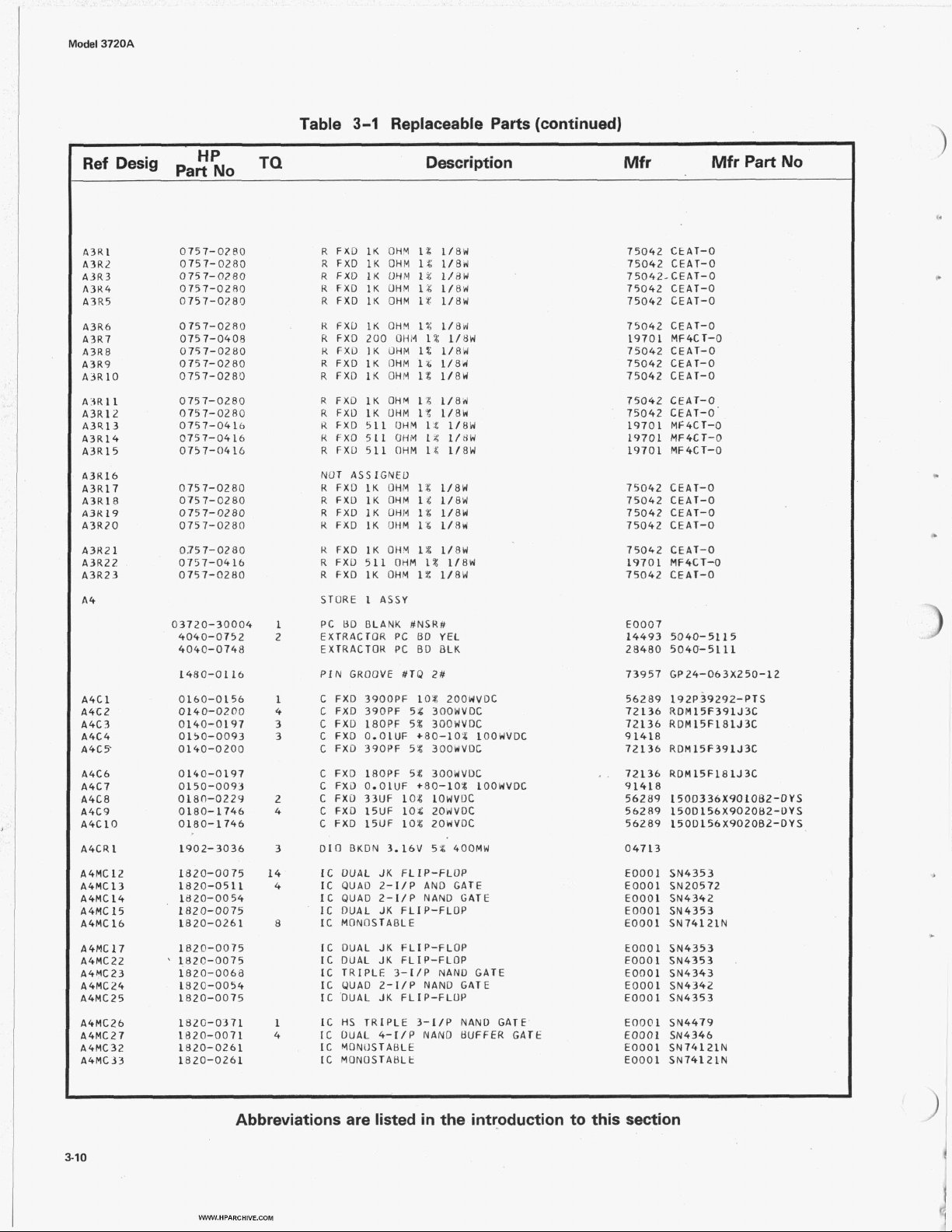
A3Rl
A3RL
A3R3
A3R4
A3R5
A3R6
A3R7
A3R8
A3R9
AM10
AiR11
A3RlL
A3Q13
A3R14
AJRl5
A3K16
A3R17
A3R18
A3K19
A3R20
A3H21
A3R22
A3R23
A4
1
A4C
A4C2
A4C3
A4C4
A4CY
A4C6
A4C7
A4C8
A4C9
A4C 10
A4CR
1
A4MC 12
A4MC 13
A4MC 14
A4MC 15
A4MC 16
A4MC17
A4MC22
A4MC23
A4MC24
A4MC 25
A4MC26
A4MC27
A4MC32
A4MC33
0757-0180
0757-0280
0
75 7-0280
0757-0280
0
75 7-02
0
75 7-02
0757-0408
0757-0280
0
757-0280
0757-0280
0757-0280
0
75 7-0280
0
75 7- 04
075 7-04 16
0737-0416
0757-0280
075 7-02
0757-0280
0757-0280
0.75 7-0280
0757-0416
0
75
7-
02
03720-30004
4040-0732
4040-0748
1480-0
1
0160-01 56
0
140-0200
0140-0 197
0150-0093
0140-0200
0140-0197
0150-0093
0180-0229
0
180- 1746
0180-1746
1902- 3036
18
20-
00
1820-051
Id 20-00 54
1820-0075
1820-0261
1820-0075
‘
1820-0075
1820-0068
1820-0054
1820-0075
1620-03 71
1820-007
1820-0261
1820-0261
80
80
16
80
80
16
?
5
I
1
1
2
1
4
3
3
2
4
3
14
4
8
1
0
Table
3-1
Replaceable Parts (continued)
R
FXD
K
OHM
R
FXD
R
FXD
R
FXD
R
FXD
H
FXD
1K
R
FXD 200
K
FXD 1K
R
FXD
1K
R
FXD
1K
R
FXD
1K
R
FXD
1K
K
FXD 511
H
FXD 511
R
FXD 511 OHM
NUT ASSfGNED
R
FXD
1K
R
FXD 1K
R
FXD
1K
K
FXD 1K OHM
K
FXD
1K OHM
R
FXL)
511
R
FXD
1K
STORE
1
PC
BD
BLANK #NSRt
EXTRACrOR PC BD YEL
EXTRACTOR PC BD BLK
PIN GROOVE
C
FXD 3900PF
C
FXD 390PF 53 3OOWVDC
C
FXD l8OPF 5% 300WVDC
C
FXD 0.OIUF
C
FXD 390PF 5% 300WVDC
C
FXO l8OPF 5% 3OOWVDC
C
FXD
0.OlUF +80-10% IOOUVDL
C
FXO 33UF
C
FXD 15UF
C
FXD 15UF
OIO
BKDN
IC
DUAL JK FLIP-FLOP
IC
QUAD 2-I/P AND GATE
IC
WAD
IC
DUAL
IC
MONOSTABLE
IC
DUAL JK FLIP-FLOP
IC
DUAL
IC
TRIPLE 3-I/P NAND GATE
IC
WAD 2-I/P NAND GATE
IC
’DUAL
IC
HS
TRIPLE 3-1/P NAND GATE
IC
DUAL 4-I/P NAND 6UFFER GATE
IC
MONIJSTABLt
IC
MONOSTAHLt
1%
K
OHM
1%
K
UH+i
1%
K
OHM
14
K
OHM
1%
OHM
1%
1/64
OHM
1%
UHM
1%
OHM
#T4
1%
1%
1%
1%
1Y
It;
1L
18
ld
1%
1%
1%
1%
1%
2#
10%
1/8W
1/84
1/8W
1/8W
1/8U
1/8W
1/8W
2OOUVOC
OHM
OHM
OHM
OHM
OHH
OHM
OHM
OHM
OHM
OHM
ASSY
+80-101
10%
IOWVDC
10%
ZOWVDC
10%
ZOWVDC
3.16~ 51 400~11
2-I/P NANO GATE
JK
FLIP-FLOP
JK
FLIP-FLOP
JK
FLIP-FLOP
1/8W
i/en
IOOWVOC
75042 CkAT-0
75042 CEAT-0
75042-CEAT-0
75042
CEAT-0
75042
CEAT-0
75042 CEAT-0
19701 Mf4CT-0
75042 CEAT-0
75042 CEAT-0
75042 CEAT-0
75042 CEAT-0,
75042 CEAT-0
1970
1
MF 4CT-0
19701
MFQCT-0
19701 MF4CT-0
75042 CEAT-0
75042 CEAT-0
75042 CEAT-0
75042 CEAT-0
75042 CEAT-0
MF~CT-O
19701
75042 CEAT-0
E0007
14493 5040- 51
28480 5040-5111
73957 GP24-063x250-12
56289 192P39292-PTS
72136 RDM15F391J3C
72136 RDM15F181J3C
9 1418
72136 RDM15F391J3C
72136 RDMl5F181J3C
91418
56289 15OD336X901062-DYS
56289 150DlS6X902062-DYS
56289 150D156X902082-DYS
04713
EOOOl St44353
€0001 SN20572
EOOOl SN4342
EOOOl
SN4353
€0001 SN74121N
EO001 SN4353
EOOOl SN4353
€0001
SN4343
€0001 SN4342
EOOOl SN4353
EOOOl SN4479
EO001 SN4346
EOOOl
SN74121N
€0001
SN74121N
15
3-10
Abbreviations are listed in the introduction to this section
WWW.HPARCHIVE.COM
Page 31

Table
3-1
Replaceable Parts (continued)
Ref
Desig Part
A4MC34
A4MC 36
A4MC 37
A4MC42
A4MC43
A4MC44
A4MC45
A4MC46
A4MC47
A4MC51
A4MC52
A4MC
53
A4MC54
A4MC55
A4MC5b
A4MC 57
A4MC61
A4MC62
A4MCb3
A4MC64
A4MC65
A4MCb6
A4MC67
A4Q
1
A4Q2
A492
A403
A4Q4
A4Q5
A406
A4R1
A4K2
A4R3
A4K4
A4RS
A4R6
A4R7
A4R8
A4R8
A4R9
c
n
A4R9
A4R
10
A4R11
A4R12
A4R
13
A4R14
A4R15
A4R16
A4R17
A5
HP
1820-0054
1820-0370
1820-0054
182 0-0770
1820-07
1820-0770
1820-0770
1820-0770
1620-0770
182
0-0077
1820-0328
1820-
1820-0328
1820-0328
1820-0328
1820-0328
1820-0328
1820-0072
1820-00 72
1
82
0-
1820-0072
1820-0072
1820-0072
1853-0036
1854-0045
1854-0045
1853-0036
18 53-0036
1
8
54- 0045
1853-0036
0757-0280
06980698-4636
075
7-
0757-0280
0698- 3 155
0698-4636
0757-0284
0757-0284
075 7-0280
075 7-0280
075 7-02
075
7-0280
0698- 5490
0
757-0280
0
75
7-
0
75
7-
0698-5490
0698-5490
03720-30005
4040-0753
4040-0748
No
70
0
32
8
00
72
3
155
0284
80
02
8
0
02
80
TQ
1
5
Description
IC
QUAD 2-1/P NAND GATE
IC
HS
QUAD 2-I/P NAND GATE
IC
QUAD 2-IIP NAND GATE
IC DUAL 100-BIT SHIFT REGISTER
IC DUAL 100-BIT SHIFT REGISTER
IC DUAL 100-BIT SHIFT REGISTER
IC DUAL 100-BIT SHIFT REGISTER
IC DUAL 100-BIT SHIFT REGISTER
IC
DUAL 100-BIT SHIFT REGISTER
IC OUAL 0-TYPE FLIP-FLOP
IC
QUAD 2-I/P
IC QUAD
IC
QUAD 2-I/P NOK GATE
IC
OUAO
IC QUAD 2-I/P NOH GATE
IC QUAD
IC
OUAD 2-I/P NOK GATE
IC
DUAL 2-WIDE Z-I/P AND/INY +XR GATE
IC
DUAL 2-WIDE 2-I/P AND/INV +XR GATE
IC
DUAL 2-WIDE 2-1/P AND/INV +XR GATE
IC OUAL 2-WIDE 2-I/P ANDIINV +XR GATE
OUAL 2-WIDE 2-I/P
IC
DUAL 2-HIDE 2-I/P
IC
SI
XSTK
SI
XSTR
SI
XSTH
3
XSTK
SI
XSTR
SI
SI
XSTR
XSTR
SI
R FXD 1K
R FXD 4.64K
8
R FXD 2.61K OHM
2
4
R FXD 150 OHM
K
FXD
IK
R FXD 4.64K
R FXD 2.61K
R
FXD 150
R FXD 150
R FXD 1K
K FXD 1K
R FXD 1K OHM
R FXD
1K
R FXD 2K
R FXD 1K OHM
R
FKD 1K
R FXD 1K OHM
R FXD 2K
R FXD
2K
STORE 2 ASSY
PC BO BLANK #NSR#
1
EXTRACTOK PC
2
EXTRACTOR PC OD 8L.K
NOR
2-IIP NOR GATE
2-I/P NOR GATE
2-I/P NOR GATE
PNP
NPN
NPN
PNP
PNP
NPN
PNP
OHM
1%
1/8W
OHM
18
1%
ow
19:
i/8w
OHM
1%
OHM
1%
OHM
1%
UHH
1%
OHM
1%
1/8H
OHH
1%
1/8W
1%
1%
1%
1%
1%
1%
1%
1%
RD
1/8W
1/8W
1/8#
1/8W
1/8W
1/8W
1/8W
GRN
OHM
OHM
OHM
OHM
OHM
GATE
AND/INV +XR GATE
ANDIINV +XR GAlE
13
1/8M
1/4W
1/8W
1/8W
1/4W
1/8W
1/8W
1/8W
Mf
r
EOOOl SN4342
€0001
EOOOl SN4342
12040 MM5006H
12040 MM5006H
12040
12040
12040 MM5006H
12040 MM5006H
EOOOl SN4354
EO001 SN4467
EO001 SN4467
EO001 SN4467
€0001 944467
EO001 SN4467
€0001 SN4467
EO001 SN4467
EO001 SN43+7
EOOOl SN4347
EO001 SN4347
EOOOl SN4347
€0001 SN4347
€0001
04713
07933 RT4299
07933
04713
04713
07933
04713
75042 CEAT-0
19701
91637
75042 CEAT-0
75042 CEAT-0
19701
91637
75042 CEAT-0
75042 CEAT-0
75042 CEAT-0
75042 CEAT-0
75042 CEAT-0
75042 CEAT-0
91637
75042 CEAT-0
75042 CEAT-0
75042 CEAT-0
91637
91637
E0007
14493
28480 5040-5111
Mfr
SN4478
MM5OObH
MM5006H
514347
t2N3906Y 585-3612
RT4299
X2N39061 SPS-3612
W2N3906Y SP5-3612
UT4299
12N3906Y SPS-3612
MF4CT-0
MFF-1/8-32T-l
MF4CT-0
MFF-1/8-32T-1
CMF-1/10-32T-Z
CMF-1/10-32T-2
CMF-1/10-321-2
5040-5116
Part
No
WWW.HPARCHIVE.COM
Abbreviations are listed in the introduction
to
this section
3.1
1
Page 32

M#k)
372OA
Ref Part
A5C1
A5C2
A5CR
1
A5MCll
A5MC12
A5YC 13
A5MC14
A5MCl5
A5MC
16
ASK21
A5YC22
A5MC23
A5YC24
A5MC25
A5YC26
A5MC31
A5MC32
A5MC33
A5MC34
A5MC35
A5MC 36
A5MC41
A5MC42
A5MC43
A5MC44
A
5MC45
A5MC46
A5MC51
A5MC52
A5MC53
A5YC54
A5MC55
A5MC 56
A5MC61
A5HCh2
A5HC63
A5MCh4
A5MC65
A5MChB
A5R1
A6
46C1
4662
46CR
1
46MC 14
HP
1
48
0
180-0229
0180- 1746
1902-3036
1820-0305
1820-007
1820-0305
1820-0054
1
82
1820-007
1820-02
1810-0282
1820-02 82
1820-0282
1820-0282
1820-0282
1820-0072
1820-0072
18
2
1820-0072
1820-0072
1820-0072
1820-0770
1820-0770
182
1820-0770
1820-0770
1R2O-0770
1820-0328
1820-0328
1820-0328
l82O-032d
1820-0328
18ZO-0328
1620-0072
182
1820-0072
1820-0072
1
8
2
1820-0072
0698-5490
03720- 30006
4040-0754
4040-0748
1460-0
0180-01
0180-0
1902-3036
1820-0054
NO
0-
0
0-
03
0-00
0-
077
0-
00
0-
00
1 1
0
82
72
72
7
1
16
16
116
Table
3-1
TQ
6
1
5
1
0
2
PIN GROOVE #TQ
C
FXD 33UF
C
FXD 15UF 10% ZOIJVDC
DID
tlKDN 3.16V 5Z 400MW
3
IC
4-BIT ADDER
IC
DUAL 4-I/P NAND BUFFER GATE
IC
4-BIT ADDER
IC
QUAD 2-I/P NAND GATE
IC
4-BIT ADDEg
DUAL 4-I/P
IC
6
1
2 EXTRACTOR PC BD BLU
QUAD 2-I/P
IC
IC
QUAD
IC
QUAD
QUAD L-I/P
IC
IC
QUA0 2-I/P EXCLUSIVE
IC
QUAD'2-I/P EXCLUSIVE OR GATE
IC
OUAL 2-dIDE 2-I/P AND/INV +XR GATE
IC
DUAL 2-WIDE 2-I/P AND/INV +XR GATE
IC
DUAL 2-WIDE 2-1IP AND/INV +XK
IC
DUAL 2-WIDE Z-I/P AND/INV +XR GATE
IC
DUAL 2-WIDE 2-I/P AND/INV +XR GATE
IC
DUAL 2-WIDE 2-I/P AND/INV +XR GATE
IC
DUAL 100-BIT SHIFT REGISTER
C
DUAL 100-BIT SHIFT REGISTER
C
DUAL 100-BIT SHIFT REGISTER
C
DUAL 100-BIT SHIFT REGISTER
C
DUAL
C
DUAL 100-RIT SHIFT HEGISTEK
C
QUAD 2-I/P NOH GATE
C
QUAD
C
QUAD
C
QUAD
IC
QUAD
QUAD
IC
DUAL
IC
IC
DUAL
IC
DUAL 2-WIDE
IC
DUAL
DUAL 2-WIDE
IC
IC
DUAL 2-WIDE 2-1/P AND/INV
R FXD 2K OHM
BUFFEA ASSY
PC OD RLANK #NSR#
EXTRACTOH PC BD BLK
PIN GROOVE #TO 2#
C
FXD 6.8UF
C FXD 6.8UF
DIU
BKDN 3.16V
IC
QUAD 2-I/P NAND GATE
Replaceable Parts (continued)
Description Mf r Mfr Part
2d
lo&
lOkVDC
NAND BUFF€& GATE
EXCLUSIVE OR GATE
2-I/P
EXCLUSIVE
2-I/P EXCLUSIVE OR GATE
EXCLUSIVE OR GATE
100-BIT
2-IIP NOR
2-I/P NOR
2-1/P NOR GATE
2-I/P
2-I/P NOR
2-WIDE
2-WIDE 2-I/P
2-WIDE
SHIFT REGISTER
NOR GATE
2-I/P AhlD/lNV
2-1/P ANO/INV
2-IIP AND/INV
2-I/P AND/INV +XR GATE
1%
1/8W
10%
35WVDC
10%
35WVDC
5%
IIK
GATE
OK
GATE
GATE
GATE
GATE
AND/INV +XR GATE
400MW
+XR GATE
+XR GATE
+XR GATE
+XR
GATk
GATE
73957 GP24-063x250-12
56289 150D336X901OR2-DYS
56289 150D156X902082-DYS
04713
EO001 SN4465
EO001 SN4346
EO001 SN4465
E0001 SN4342
€0001
SN4465
EOOOl SN4346
€000
1
SN 13603
EO001 SN13603
EOOOl SN13603
EO001 SN13603
EO00
1
SN 13603
EOOOl SN13603
E0001 SN4347
E0001 SN4347
EO001 SN4347
€0001
SN4347
€0001
SN4347
€0001 SN4347
12040 MH5006H
12040 MM5006H
12040 MM5006H
12040 MB5006H
12040 MM5006H
12040 MM5006H
E0001 SN4467
SN4467
€000
SN4467
EO00
SN4467
EO00
SN4467
EO00
SN(4467
EO00
SN4347
E000
SN4347
EO00
SN4347
€000
SN4347
€000
ED001 SN4347
EOOOl SN4347
91637 CMF-l/lO-32T-2
E0007
14493 5040-5117
28480 5040-5111
73957 GP24-063x250-12
56289 150D685X903582-DYS
56289 150D685X903582-DYS
04713
EO001 SN4342
No
6
r)
912
Abbreviations are listed in the introduction to this section
WWW.HPARCHIVE.COM
Page 33

Ref
Dmig Part
”’
No
TQ
Table
3-1
Replaceable Parts (continued)
Description Mf r Mfr
Part
No
A6MC21
A6MC22
A6MC23
A6MC24
A6MC25
A6MC26
A6MC31
A6MC32
A6MC33
A6MC 34
A6MC35
A6MG 36
A6MC46
A6R1
A6R2
A6R3
A6K4
A6RS
A6R6
A6R7
A6R8
A6R9,
A6RlO
A6R11
AbR12
A6R 13
A6Rl4
A6R15
A6R
1
b
A6R17
A6R18
A6RlY
A6R20
A6R2
1
A6R22
A6R23
A6R24
A6R25
A6R26
A6R27
A6R28
A6R29
A6R30
A6R
3
1
A6R32
A6R33
A6R34
A7
A7C1
1820-01 07
1820-0054
1820-0054
1820-0077
1820-0 107
1820-0054
1820-0107
1820-0054
182
0-0
107
1820-0054
1820-0107
1820-0068
1820-0328
0698-5490
0757-0280
0698-5490
0
75
7-
02
75
7-
02
6
9
8-
54
75 7-0280
75 7-0280
16
0-
2204
80
ao
80
9
0698-5490
0757-0280
0698-5490
0757-0280
0698-5490
075 7-02
0698-5490
0757-0280
0698-5490
0757-0280
0698-5490
0757-0280
0698-5490
075 7- 0280
0698-5490
0
0698- 5490
0757-0280
0698-5490
0757-02ao
0698-5490
0757-0280
0
0757-0280
075 7-0280
0757-0280
0698-5490
0757-0280
0
0
03720-30007
4040-0755
4040-0749
1480-01 16
0
5
0
1
1
11
18
QUAD INTERFACE BUFFER GATE
IC
OlJAD
IC
IC
IC
IC
IC
IC
IC
IC
IC
IC
IC
IC
R
R
R
R
R
R
R
R
R
R
R
K
R
R
R
R
R
R
R
R
R
R
R
R
R
R
R
R
R
R
R
R
R
R
SWITCH CARD
PC
EXTRACTOR
EXTRACTOR PC
PIN GROOVE
C
2-I/P NAND GATE
QUAD 2-IIP NAND GATE
DUAL D-TYPE FLIP-FLOP
QUAD INTERFACE BUFFER GATE
UUAD 2-IIP NAND GATE
QUAD INTERFACE BUFFER GATE
QUAD 2-I/P NAN0
QUAD INTERFACE BUFFER GATE
QUAD
Z-I/P
QUA0 INTERFACE BUFFER GATE
TRIPLE 3-1/P NAND GATE
QUAD 2-I/P NOR GATE
FXD 2K
FXD
FXD 2K
FXD 1K
FXD 2K
FXD 1K
FXD 2K
FXD 1K
FXD 2K
FXD
FXD 2K
FXD 1K
FXD 2K
FXD 1K
FXD 2K
FXD 1K
FXD 2K
FXD
FXD 2K
FXD
FXD
FXD 1K
FXD 2K
FXD
FXD 2K
FXD
FXD
FXD
FXD
FXD
FXD 2K
FXD
FXD
FXD
RD
FXD lO0PF 5% 3OOYVDC
OHM
1K
OHM
OHM
OHM
OHM
OHM
OHM
OHM
OHM
1K
OHM
OHM
OHM
OHM
OHM
OHM
OHM
OHM
1K
OHM
OHM
OHM
i~
OHM
2K
OHM
OHM
IK
OHM
OHM
1K
OHM
OHM
2K
1K
OHM
1K
OHM
1K
OHM
OHM
1K
OHM
1K
OHY
1K
OHM
ASSY
BLANK #NSR#
PC
#TO
GATE
NAND GATE
1%
1/8W
1%
1/8W
1%
1/8W
1%
1/8W
1%
1/8W
1%
1/84
1%
1/8Y
1%
1/BW
1%
1/8W
1%
1/8H
1%
1/8W
1%
1/8U
1%
1/8W
1%
1/8ti
1%
1/8W
1%
1/8d
1%
l/8Y
1%
1/8W
1%
1/8W
1%
i/8n
1%
1/8Y
1%
1/8U
1%
1/8U
1%
1/8Y
1Z
1/8W
1%
1/8W
1%
1/8Y
1%
1/8W
1%
1/8W
1%
1/BW
1P
1/8W
1%
1/BW
1%
1/8Y
1%
l/8W
BD
VI0
BO
BRN
2#
14493 8902-5080
EO001 SN4342
€0001
SN4342
€0001 SN4354
14493 8902-5080
€0001 SN4342
14493 8902-5080
EO001 514342
14493 8902-5080
€0001 SN4342
14493 8902-5080
EO001 SN4343
€0001 SN4467
91637 CMF-1/10-321-2
75042 CEAT-0
9
1637 CMF-l/10-32T-2
75042 CEAT-0
91637 tMF-1/10-321-2
75042 CEAT-0
91637 tMF-1/10-32T-2
75042 CEAT-0
91637 CMF-1/10-3ZT-2
75042 CEAT-0
91637 CMF-1/10-32T-2
75042 CEAT-0
91637 CMF-1/10-32T-2
75042 CEAT-0
91637 CMF-1/10-32T-2
75042 CEAT-0
91637 CMF-1/10-32T-2
75042 CEAT-0
91637
EMF- I /10-321-2
75042 CEAT-0
91637 tMF-1/10-32T-2
75042 CEAT-0
91637
CMF-1/10-321-2
75042 CEAT-0
9 1637 CMF-1/10-321-2
75042 CEAT-0
91637 CMF-l/lO-32T-2
75042 CEAT-0
75042 CEAT-0
75042 CEAT-0
91637 CMF-1/10-321-2
75042 CEAT-0
75042 CEAT-0
75042 CEAT-0
E0007
14493 5040-5118
14493 5040-5112
73957 GP24-063x250-12
72136 RDM15FlOlJ3C
WWW.HPARCHIVE.COM
Abbreviations are listed in the introduction to
this
section
3-13
Page 34

Table
3-1
Replaceable
Parts (continued)
Ref part
A7C2
A7C3
A7Cll
A7C 12
A7Cl3
A7C21
A7C22
A7C23
A7C31
A7C32
A7C33
A7C41
A7C42
A7C43
A7C51
A7C52
A7C53
A7C6
1
A7C62
A7C63
A7C71
A7C72
A7C73
A7C81
A7C82
A7683
A7C9
1
A7C92
A7C93
A7C101
A7C102
A7C103
A7C111
A7C112
A7C113
A7C121
A7C12.2
A7CR1
A7CR2
A7CR
11
A7CR 12
A7CR21
A7CR22
A7CR31
A7CR32
A7CR41
A7CR42
A7CR51
A7CR52
A7CR61
A7CR62
A7CR7
1
A7CR72
A7CR81
A7CR82
HP
0160-0333
0160-0333
0160-2204
0160-0333
0160-0333
0
160-2204
0
160-0333
0
160-0333
0
160-
0160-0333
0
160-0333
0160-2204
0160-0333
0160-0333
0
16
0160-0333
0
16
0
160-2204
0
160-0333
0
160-033
0
16
0160-0333
0
160- 03 33
0
16
0160-0333
0
160-033 3
0160-2204
0160-0333
0160-0333
0160-2204
0160-0333
0160-0333
0
16
0
160- 03 33
0160-0333
0180-0116
01
80-01 16
1901-0040
1901-0040
190 1-0040
1901-0040
190 1-0040
190
190
1901-0040
1901-0040
1901-0040
1901-0040
190 1-0040
1901-0040
1YO1-0040
190 1-0040
190
1901-0040
1901-0040
NO
2
2
04
0-
2
204
0-
03 3 3
0-2
204
0-
2204
0- 2 2
04
1-0040
1-0040
1-
0040
TQ Description Mf r Mfr Part
24
3
‘C
.
15PF 0.5PF 300WVDC
C
FXD
FXD l5PF 0.5PF 3OOWVDC
C
FXD 1OOPF 5% 300WVDC
C
15PF 0.5PF 3OOWVDC
C
FXD
C
FXD 15PF 0.5PF 3OOWVDC
C
FXO lOOPF
C
FXD 15PF 0.5PF 3OOWVDC
C
FXD 15PF 0.5PF 300WVDC
C FXD lOOPF
C
FXD l5PF 0.5PF 300rlVDC
C
FXD 15PF 0.5PF 300WVDC
C
FXD lOOPF 5% 300WVDC
C
FXD 15PF 0.5PF 300WVDC
C
FXD 15PF 0.5PF 3OOWVOC
C
FXD 1OOPF 5% 3OOWVDC
C
FXD 15PF 0.5PF 300WVDC
C
FXD 15PF 0.5PF 300WVDC
C
FXD lOOPF 5% 300rlVDC
C
FXD l5PF 0.5PF 3OOHVDC
FXD 15PF 0.5PF 300WVDC
C
FXD IOOPF 5% 300WVOC
C
FXD 15PF 0.5PF 300dVDC
C
FXD 15PF 0,5PF 3OOUVDC
C
FXD 1OOPF 5% 300WVDC
C
FXD 15PF 0.5PF 300WVDC
C
FXD
C
FXD lOOPF 5% 300WVDC
FXD 15PF 0.5PF 300WVDC
C
FXD 15PF 0.5PF 300WVDC
C
C
FXD LOOPF
C
FXD 15PF 0.5PF 300WVDC
C
FXD 15PF 0.5PF 3OOHVDC
C
FXD 1OOPF 5% 3OOIJVDC
C
FXO 15PF 0.5PF 3OOWVDC
C
FXU 15PF 0.5PF 3OOWVDC
C
FXD 6.8UF
C
FXD 6.8UF
DID
SI
DIO
SI
DIO
SI
DIU
SI
DIO
SI
010
SI
DIO
SI
010
SI
DID
SI
010
SI
DIO
SI
DIO SI
DID
SI
DIO
SI
DIO
SI
010
SI
DIO
SI
010
SI
5%
300HVDC
5%
300UVOC
15PF 0.5PF 300WVDC
5%
3OOWVDC
10%
35WVDC
10%
35WVDC
72136 RDM15C150D3C
72
1
36 RDM 15.C 150D3C
72136 RDM15FlOlJ3C
72136 RDM15C150D3C
72 136 RDM15C15OD3C
72136 RDM15FlOlJ3C
72136 RDM15C150D3C
72136 RDM15C150D3C
72136 RDM 15F
721 36 RDR 15C 150D3C
72136 RDM15Cl50D3C
72136 RDMl5FlOlJ3C
72136 RDM15C150D3C
72136 RDH15C15003C
72136 KDM15FlOlJ3C
72 136 RDM 15C 150D3C
72136 RDH15C15003C
72 136 RDM 15F101J 3C
72136 RDM15C150D3C
72136 RDM15C150D3C
72136 RDM15F101J3C
72136 ROM15C150D3C
72 136
RDM
72136 RDH15F101J3C
72136 RDH15C150D3C
72 136 RDH15615003C
72136 RDM15FlOlJ3C
72136 ROR15C150D3C
72136 KDH15C150D3C
72136 RDM15FlOlJ3C
72136 HDM15C15DD3C
72136 RDM15CL50D3C
72136 RDMl5FlOlJ3C
72136 RDM15C150D3C
7
2
136 RDW 15C 150D3C
562 89 15006 85X903582-DYS
56289 1500665X903562-DYS
12065 565050
12065 565050
12065 565050
12065 565050
12065 565050
12065 565050
12065 565050
12065 565050
12065 565050
12065 565050
12065 565050
12065 SG5050
12065 565050
12065 565050
12065 565050
12065 565050
12065 565050
12065 565050
10
1
15C 1501336
No
J3C
r)
c
3-14
Abbreviations are listed in the introduction to this section
WWW.HPARCHIVE.COM
c
4
Page 35

Section
111
2
Ref Part
A7CR91
A7CK92
A7CR10
A7CR10
A7CR111
A7CK112
A7U1
A7612
A7Q3
A
794
A705
A7911
A7912
A7Q13
A7914
A7915
A7821
A7822
A7923
A7824
A7925
A7931
A7932
A7933
A7934
A7935
A7041
A7942
A7943
A7944
A
704
5
A7951
A7952
A7953
A7954
A7955
A
796
1
A7962
A7963
A7864
A7Q65
A7971
A7Q72
A7973
A7074
A7Q75
A798
1
A7982
A7Q83
A7984
A7985
A799
1
A7092
A7993
A7994
1YO
1901-0040
190 1-0040
190
190 1-0040
1901-0040
185 41853-0036
1854-02
18
5
1855-0020
1854-001 9
1853-0036
1854-02 15
1855-0020
1855-0020
1854-0019
18 53-0036
18
54- 02 15
1855-0020
1855-0020
1854-0019
1853-0036
1854-02 15
1855-0020
1855-0020
18 54-001 9
I8 5 3-003
18
5
1855-0020
1855-0020
1854-0019
18 53-0036
1854-02 15
1855-0020
1855-
1854-0019
1853-0036
1854-0215
1855-0020
1855-0020
1854-00
1853-0036
18 54-02 15
1855-0020
1855-0020
18 54185 3-003 6
1854-0215
1855-0020
1855-0020
18 54- 00
18 53-0036
1864- 02 1
1855-0020
"'
NO
1-0040
1-0040
00
5-
0
'I20
4- 02
0020
00
Table
3-1
Replaceable Parts (continued)
TQ Description
010
SI
DIU
SI
DIU
SI
DIU
SI
DIU
SI
010
SI
19
16 XSTR
I5
67 XSTR Ft
6
I5
19
19
1
9
5
XSTR
XSTR
XSTK
XSTR
XSTR
XSTR
XSTK
XSTR
XSTR
XSTK
XSTR
XSTR FET &-CHANNEL
XSTR
XSTR
XSTR
XSTR
XSTR
XSTR FET N-CHANNEL
XSTK
XSTR
XSTR
XSTR FET N-CHANNEL
XSTR
XSTR
XSTR
XSTR
XSTR
XSTR
XSTR
XSTR
XSTR
XSTR FE
XSTK FE
XSTR
XSTR
XSTK
XSTK
XSTR
XSTR
XSTR
XSTR
XSTR
XSTR
XSTR
XSTH
XSTR
XSTR FET N-CHANNEL
NPhl
SI
PNP
SI
NPN
SI
N-CHANNEL
N-CHANNEL
FE
NPN
SI
PNP
SI
NPN
SI
N-CHANNEL
FE
N-CHANNEL
FE
NPN
SI
PNP
SI
SI
NPN
FET N-CHANNEL
SI
NPN
SI
PNP
SI
NPN
FET N-CHANNEL
SI
NPN
SI
PNP
SI
NPN
FET N-CHANNEL
SI
NPN
SI
PNP
SI
NPN
FET N-CHANNEL
FET N-CHANNEL
SI
NPN
PNP
SI
NPN
SI
N-CHANNEL
N-CHANNEI
NPN
SI
PNP
SI
NPN
SI
N-C HA NNEL
FE
N-CHANNEL
FE
SI
NPN
SI
PNP
SI
NPN
FET Y-CHANNEL
FET N-CHANNEL
SI
NPN
SI
PNP
SI
NPN
Mf
r
12065 565050
12065 SG5050
12065 SG5050
12065 565050
12065 565050
12065 SG5050
13715 5-6516
04713 #2N3906# SPS-3622
04713 SPS3611
21845 F1151
21845 F1151
13715 S-6516
04713 #2N3906# SPS-3612
04713 SPS3611
21845 F1151
21845 F1151
13715 5-6516
04713 #2N3906# SPS-3612
04713 SPS3611
21845 Fll5l
21845 F1151
13715 5-6516
04713 #2N3906# SPS-3612
04713 SPS3611
21845 F1151
21845 F1151
13715
04713 #2N3906# SPS-3612
04713 SPS3611
21845 F1151
21845 F1151
13715 5-65-16
04713 #2N3906#
04713 SPS3611
21845 F1151
21845 F1151
13715 5-6516
04713 #2N3906# SPS-36
04713 SPS3611
21845 F1151
21845 F1151
13715 5-6516
04713 #2N3906# SPS-36
04713 SPS3611
21845 F1151
21845 F1151
13715 5-6516
04713
04713
2 1845
21845
13715
04713
04713
21845
Mfr Part
5-6516
SP
5-3612
#2N3906# SPS-3612
SPS3611
F1151
F1151
5-65-16
#
2 N 3
906 # SP
SPS3611
F1151
S-
36
No
12
WWW.HPARCHIVE.COM
~~
Abbreviations are listed in the introduction to this section
3-15
Page 36

Modd
372QA
.
...
.
.
.
.,
.~.
.. ..
.
. ..
.
.
.
-.-
.
~
.
.
.
'
.
.
. . . -.
.
__~__
Ref
A7895
A761101
A7U102
A78103
A7Q104
A7Q105
A701
11
A78111
A7J113
A70114
A70115
A7R
1
A7R2
A7R3
A7R4
A7R5
A7R6
A7R7
A7R8
A7R9
A7Rll
A7R12
A7R13
A7R14
A7R15
A7R16
A7K17
A7R18
A7R19
A7R2
1
A7R22
A7R23
A7R24
A7R25
A7R26
A7R27
A7R28
A7R29
A7R31
A7R32
A7R33
A7R34
A7R35
A7R36
A7R37
A7R38
A7R39
A7R41
A7R42
A7R43
A7R44
A7R45
A7R46
A7R47
A7R48
Part
"'
No
1855-0020
1854-00
1853-0036
1854-021
1855-0020
185 5-0020
1854-0019
1853-0035
18
185
1855-0020
0698-5490
0698-5490
0698-3446
06980757-0750
0757-0449
0
0757-0465
0757-0482
0698-5490
0698-5490
0698-3446
Oh98-3 153
0757-0750
0757-0449
0
0
0
0698-5490
0698-5490
0698-3446
0698-31 53
0757-0750
0
0757-0750
0
0757-0482
0698-5490
0698-5490
0698-3446
0698- 3
0
75 7-0750
0757-0449
0757-0750
0757-0465
0757-0482
0b98-5490
0698-5490
0698-3446
0698-3153
0757-0750
0757-0449
0757-0750
0757-0465
19
54-02 15
5-0020
3
153
75 7- 0 750
757-0 750
757-0465
75 7- 048
75 7-0449
75 7- 0465
1
53
Table
3-1
Replaceable Parts (continued)
TO Description
XSTR
FET N-CHANNEL
XSTR
5
55
42
51
13
91
18
2
XSTR
XSTK
XSTK
XSTR
XSTR
XSTR
XSTR
XSTK
XSTR
R
R
R
R
R
R
K
K
R
R
R
R
R
K
R
R
R
R
R
R
k
R
R
R
R
R
K
R
R
R
R
R
R
FXD
R
R
R
R
R
FXD ZK OHM
R
FXO 383 OHM
R
FXI) 3.83K OHM
R
FXO 6.81K OHM
K
FXO 20K OHM
R
FXD 6.81K OHM
R
FXO lOOK 13HM
NPN
SI
SI
PNP
NPN
SI
N-C
FE
FE
SI
SI
SI
FE
FE
FXD 2K
FXO 2K
FXD 383 OHM
FXO 3.83K UHM
FXO
FXD LOK OHM
FXO
FXD 1OOK OHM
FXD 511K
FXD 2K OHM
FXD 2K OHM
FXD 383 OHM
FXO
FXD 6.81K OHM
FXO
FXU 6.81K OHM
FXO
FXO 511K OHM
FXD 2K OHM
FXD 2K
FXO 383 OHM
FXD 3.83K OHM
FXD 6.81K OHM
FXD ZOK OHM
FXD 6.81K
FXD
FXD 511K OHM
FXD 2K OHM
FXO 2K OHM
FXD
FXO 3.83K OHM
FXD
FXD 6.81K
FXD
FXD 511K OHM
FXO 2K OHM
N-CHANNEL
NPY
PNP
FlPN
N-CHANNEL
N-CHANNEL
OHM
OHM
6.81K
6.81K
3.83K
ZOK
OHM
lOOK
OHM
lOOK
383
OHM
6.81K
ZOK
OHM
lOOK
H
OHM
OHM
OHrY
OHM
OHM
OHM
OHM
OHM
OHM
OHM
A
1%
1%
1%
1%
1I
1%
1%
1%
1%
1Z
N
N EL
1/8W
1/8rl
1%
1%
1%
1%
18
141
18
1/8W
1/8W
1%
1%
1%
1%
1%
1%
1%
1/8W
1/8Y
1%
1%
1%
1%
1%
11
11:
1/8W
1/8W
1%
1%
1%
1%
1%
11:
1%
l/8W
1/8W
1X
1%
1%'
1Z
1%
11:
1/8W
1/8W
1/4U
1/8W
1/4W
1/8H
1/8U
1/8W
1/8W
1/4W
1/8H
1/4W
1/8W
1/8W
1/8U
1/8W
1/4W
1/8H
1/4W
1/8W
1/8W
1/8W
1/8H
1/4W
1/8U
1/4U
1/8W
1/8W
1/8W
1/8W
1/4W
1/8W
114W
1/8W
Mf
r Mfr Part
21845 F1151
13715 5-6516
04713 #ZN3906# SPS-3612
04713 SPS3611
21845 F1151
21845 F1151
13715 S-6516
04713 #2N3906# SPS-3612
04713 SPS3611
21845 F1151
21845 F1151
91637 CMF-1/10-3LT-Z
91637 CMF-1/10-32T-2
19701 MF4CT-0
19701 MF4CT-0
19701 MF52CT-0
19701 MF4CT-0
19701 MF52CT-0
19701 MF4CT-0
19701 MFSC
91637 CMF-1/10-3ZT-2
91637 CMF-1/10-32T-2
19701 MF4CT-0
19701 MF4CT-0
19701 MF52CT-0
19701 MF4CT-0
19701 MF
19701 MF4CT-0
19701 MF5C
91637 CMF-1/10-32T-2
91637 CMF-1/10-321-2
19701 MF4CT-0
19701 MF4CT-0
19701 MF52CT-0
19701 MF4CT-0
19701 MF52CT-0
19701 MF4CT-0
19701 MF5C
91637 CMF-1/10-32T-2
9
1637 CNF- 1 /10-32T-2
19701 MF4CT-0
19701 MF4CT-0
19701 MF52CT-0
19701 MF4CT-0
19701 MF52CT-0
19701 MF4CT-0
19701 MF5C T-0
91637 CMF-1/10-32T-2
91637 CMF-l/ 10-321-2
19701 MF4CT-0
19701 MF4CT-0
19701 MF52CT-0
19701 HF4CT-0
19701 MF52CT-0
19701 MF4CT-0
1-0
52CT-0
1-0
1-0
,
No
516
Abbreviations are listed in the introduction to this section
WWW.HPARCHIVE.COM
c
c
Page 37

Section
111
u
H.
Ref Daig part
A7R49
A7R51
A7R52
A7R53
A7R54
A7H55
A7R56
A7R57
A7R58
A7R59
A7R61
A7R62
A7R63
A7R64
A7R65
A7R66
A7R67
A7R68
A7Rh9
A7R71
A7R72
A7R73
A7R74
A7R75
A7R76
A7R77
A7R78
A7R79
A7R81
A7R82
A7R83
A7R84
A7R85
A7R86
A7R87
A7R88
A7R89
A7R91
A7R92
A7R93
A7R94
A7R95
A7H96
A7R97
AIKC)~
A7R99
A7R101
A7R102
A7R103
A7R104
A7R105
A7R106
A7R107
A7R10t3
A7R109
HP
075 7- 0482
0698-5490
0698-5490
0698- 3446
0698-3153
0757-0750
075 7-0449
0
75 7- 0 750
0757-0465
0757-0482
0698-5490
0698-5490
0698-3446
0698-3153
0757-0750
0757-0449
0757-0750
0757- 0465
0
75 7-0482
0698-5490
069 8-5490
0698-3446
0698-3 153
0
75 7-0750
0757-0449
0757-0750
075 7-0465
075 1-0482
0698-5490
0698-5490
0698-3446
0698-3153
0757-0750
0757-0449
0757-0750
0757- 0465
0
75 7- 0482
0698-5490
0498-5490
0698-3446
Ob9R-3153
0757-0750
0757-0449
0
75 7- 0750
0757-0465
0
75 7- 048 2
06 98- 54 90
0698-5490
0698-3446
0698-3153
0757-0750
0757-0449
0
757-0750
0
757- 0465
0757-0482
Table
No
TQ Description Mf r Mfr Part
3-1
Replaceable Parts (continued)
R
FXD 511& OHM
R
FXD
ZK
R
FXD 2K
R
FXD
383
R
FXO 3.83K
FXD 6.81K OHM
R
R
FXD 20K
R
FXO
6.81~
R
FXO
IOOK
R
FXD
511~
R
FXD 2K
R
FXD 2K
R
FXD 383
R
FXD 3.83K OHM
R
FXD 6.81K OHM
R
FXD 20K
R
FXD 6.81K
R
FXD
IOOK
R
FXO 511K OHM
R
FXD 2K
R
FXD 2K OHM
R
FXD
383
R
FXD 3.83K
R
FXU 6.81K
R
FXO 2OK
R
FXD 6.81K
R
FXD
~OOK
R
FXD 511K
R
FXO 2K
R
FXD 2K
H
FXD 383 OHM 1%
R
FXL, 3.83K
R
FXD
6.81~
K
FXD
LOK
R
FXD 6.81K OHM 18 114W
R
FXD
lOOK
R
FXD 511K
R
FXD 2K
R
FXD 2K
R
FXO 383 OHM
R
FXD 3.83K
R
FXD 6.81K OHM
R
FXD 20K OHM
R
FXD 6.81K OHM 1g 1/4W
R
FXD
lOOK
R
FXO
511~
R
FXD 2K
R
FXD 2K
R
FXO 383 OHM
R
FXO 3.83K
R
FXD 6.81K
H
FXD 20K OHM
R
FXD
6.81~
R
FXD
IOOK
R
FXD
511~
OHM
OHM
OHM
OHM
OHM
OHM
OHM
OHM
OHM
OHM
UHM
OHM
OHM
OHM
OHM
OHM
OHM
OHM
OHM
OHM
OHM
OHM
OHM
OHM
OHM
OHM
OdM
OHM
OHM
1%
14:
1%
1%
OHM
1X
OHM
11:
1%
1%
1%
1Y
1%
OHM
1
1%
1%
1%
1%
OHM
OHM
1%
DHM
1%
1%
1%
1%
OHM
OHM
1%
1%
1%
1%
1%
1%
OHM
1%
1%
1'1;
1%
13:
1%
OHM
OHM
1%
OHM
1%
1%
1/8U
1/04
i/8m
1%
1%
1/8W
14
1/8W
1/8W
i/8w
1%
1%
1/8Y
1%
1/8W
1/8Y
1/84
1Z
1%
i/8m
1/8W
1/8d
1/8U
1%
1%
1/8#
1/8W
1/84
1/8W
1%
1%
1/8U
1%
1/8W
1/BW
1/4W
i/4w
1/8Y
i/8m
1/8Y
1/8W
1/4H
1/43
i/8w
1/84
1/8h
i/4n
1/8W
1/8U
1/8w
1/4W
1/8Y
i/ew
1/8W
l/4W
1/4W
1/8W
1/8n
19701 MF5C T-0
91637 CMF-1/10-3ZT-2
91637 CMF-l/10-32T-2
19701 MF4CT-0
19701 MF4CT-0
19701 MF52CT-0
19701 MF4CT-0
19701 MF52CT-0
19701 MF4CT-0
19701 MF5C T-0
91637 CMF-I/IO91637 CMF-1/10-32T-2
19701 MF4CT-0
19701 MF4CT-0
19701
HF
19701 MF4CT-0
19701 MF52CT-0
19701 MF4CT-0
19701 MF5C T-0
9 1637 CMF91637 CMF-1/10-321-2
19701 MF4CT-0
19701 MF4CT-0
19701 MF52CT-0
19701
MF4CT-0
19701 MF52CT-0
19701 MF4CT-0
19701 MF5C
9
1637 CMF-1/10-321-2
91637 CMF-1/10-321-2
19701 MF4CT-0
19701 MF4CT-0
19701 MF52CT-0
19701 MF4CT-0
19701 MF52CT-0
19701 MF4CT-0
19701 MF5C T-0
91637 CMF-1/10-32T-2
91637 CMF-1/10-32T-Z
19701 MF4CT-0
19701 MF4CT-0
19701 MF5ZCT-0
19701 MF4CT-0
19701
MF
19701 MF4CT-0
19701 MF5C T-O
9
16 37 CMF-
91637 CMF-1/10-3ZT-2
19701 MF4CT-0
19701 MF4CT-0
19701 MF52CT-0
19701 MFSCT-0
19701 MF52C.l-0
19701 MF4CT-0
19701 MF5C
5x1-0
1/
T-0
52CT-0
I/
T-0
No
10-32T-2
10-32T-2
WWW.HPARCHIVE.COM
Abbreviations are listed in the introduction to this section
3-17
Page 38

-1
Ref Desig
A7Klll
A7U112
A7R11J
A7K 114
A7R115
A7R116
A7R117
A7R118
A7R119
A8
A8C1
ABCZ
A8C3
A864
A8C5
A8C6
A8C7
A8C8
A8C9
AX10
A8Cll
A8C12
A8C13
A8C14
A81C
1
A8IC2
A8IC3
A8U1
A8R2
A8R3
A8R4
A8R5
A9
A9C
1
A9C2
A9C
3
A9C4
A9C5
A9C6
A9C7
A9C8
A9C9
A9C10
Part
"'
No
Oh98-
5490
Oh9R-5490
0098-3446
0698-3153
0757-0750
0757-0449
0757-0750
0
75
7-
0465
0
75 7-0482
0
3
72
0-
300
4040-0747
4040-0749
1480-01 16
0
160-01 74
0
160-22
0160-01 74
0
160-222 5
0
160-0 174
0160-2211
0160-0174
0
160-2 22
0180-0116
0
180-01
0160-2218
0160-2218
0
160-2197
0
160-2 198
1 8 10-
0
1820-0476
1820-0476
0698-5542
0
35
7-
045
2100-2517
0757-045
2100-2517
0
3 7 2
0-
3
40 40-
0
4040-0749
1480-0116
0
160-2 197
0
160-0 174
0
160-22
0
160-0 174
0160-2225
0
180-0
0180-01
0180-0116
0
160- 22
0
160-2 197
11
16
120
0
0
75
11
116
16
18
0
5
8
8
09
6
8
TO
63
10
Table
K
FXD 2K
R
FXU 2K
K
FXD
R
FXD 3.03K
K
FXU
R
FXD 2OK
K
FXU 6.81K
K
FXD
K
FXD 511K
HYBKIU
PC
1
1
8
9
7
6
4
1
1
BO
FXTKACTOR
EXTKACTOR
PIN GROOVE
C
FXD 0.47UF +EO-209 2 iVDC
C
FXD 510PF 5% 300WVDC
C
FXD 0.47UF +80-20% 25WVOC
C
FXD 2000PF 5% 3OOWVDC
C
FXD 0.47UF +80-20& 25WVDC
C
FXD 510PF
C
FXD 0.47UF +EO-201 25WVDC
C
FXD 2OOOPF 51 3OOWVDC
C
FXD 6.8UF
C
FXD 6-8UF
C
FXO lOOOPF 5% 300HVDC
C
FXD lOOOPF
C
FXO lOPF
C
FXD ZOPF
R
NETWORK
IC
OPER AMPL
IC
OPER AYPL
R
FXU 20K
K FXD 51.1K
R
VAR
R
FXD 51.1K
R
VAK 50K
rJINDOn MULTIPLIER
PC
BO
EXTRACTOR
EXTRACTOK
PIN GROOVE
C
FXD 1OPF
C
FXU 0.47UF +80-201 25WVDC
C
FXD 510PF 5% 3OOWVDC
C
FXD 0.47UF +BO-20% 25WVDC
C
FXD 2000PF
C
FXO 6.8UF 101 35WVOC
C
FXD 6.8UF 104: 35cJVDC
C
FXU 6.8UF
C
FXD lOOOPF
C
FXD lOPF 54 300dVOC
3-1
Replaceable Parts (continued)
Description Mf r Mfr Part
OHM
13,
1/8W
OHM
1%
OHM
OHM
UHY
OHM
UHM
OHM
OHM
PC
PC
CTQ
5%
101
10%
51:
5%
OHM
OHM
OHM
#TQ
5%
10%
1/8w
1% 1/8W
1% 1/8W
1%
1%
1/8W
1%
LX
1%
80
GUY
BD BRN
2#
3OOMVDC
35WVDC
35YVDC
5%
300WVDC
300WVDC
300WVDC
1%
1
1%
1OZ
1%
10%
ED
WHT
BO
ERN
2#
3OOWVOC
5%
300WVOC
35HVDC
5%
300WVDC
1/4w
114W
1/8W
1/8W
ASSY
RW
1/8W
/
2cJ
1/8w
12w
ASSY
783
6.81K
LOOK
MULTIPLIER
t3LANK IYNSR#
OHM
50K
OHM
BLANK YNSK#
PC
PC
No
91637 CMF-1/10-321-2
91637 CMF-1/10-32T-2
19701 MF4CT-0
19701 MF4CT-0
19701 MF52Cl-0
19701 MF4CT-0
19701 MF52tT-0
19701 MF4CT-0
19701 MF5C
E0007
28480 5040-4529
14493 5040-5112
73957 GP24-063x250-12
56289 5CllB7S-CML
72136 RDM19F511J3C
56289 5Cll87S-CMC
72 136 RDH19F20LJ3C
56289 5CllB7S-CML
72136 RDM19F511J3C
56289 5C 11875-CML
72
136
56289 1500685X903582-DYS
56289 1500685X903562-DYS
72136 RDMI9FlOLJ3C
72 136 RDM 19F 102 J3C
72 136 RDH 15ClOOJ3C
72136 KDM15C200J3C
E0013
07263 SL21384
07263
91637 CHF-l/LO-32T-9
19701 MF4tT-0
21030 62-230-1
19701 MF4CT-0
2
1030
E0007
28480 5040-5119
14493 5040-5112
73957 GP24-063x250-12
72136 RDM15C100J3C
56289 5C 1187S-CML
72136 RDH 19F511J3C
56289 5Cl 1B7S-CML
72 136 RW19F202J 3C
56289 1500685X903582-DYS
56289 150D685X903582-DYS
56289 150D685X9035BZ-OYS
72136 RDM19F102J3C
7
2
136
1-0
KDH
19F202J 3C
58CRX00 13 1R2F
5L21384
62-230-1
KDM
15C
1
OOJ
3C
.
,
Dtl
Abbreviations are listed in the introduction to this section
WWW.HPARCHIVE.COM
f
)I
Page 39

Section
111
Table
Ref Desig
A9Lll
A9C12
A9CK
1
A9CR2
A9CR3
A9CR4
A9CR5
A9CR6
A9CR7
A9CR8
A9CR9
A9CR10
A9CR
11
P
E
t
A9CRlZ
A9CR13
A9CR 14
A9CR 15
A91C1
A91C2
A9Q
1
A9Q2
A
9Q
3.
A9P4
A9Q5
A9Q6
A9Q7
A9Q8
A9Q9
A9810
A9Qll
A9812
A9Q13
A9414
A9Q15
A9Q16
A9Q17
A9Q18
A9Q19
A9Q20
A9Q2
1
A9Q22
A9Q23
A9924
A9P25
A9Q26
A9Q27
A9Q28
A9Q29
A9Q30
~9~31
A9Q32
A9R1
A9R2
A9R3
Part
HP
No
0
160-01 74
0 160-0 174
190 1-0040
190 1-0040
1901-0040
1901-0040
1901-0040
1901-0040
1901-0040
1901-0040
1901-0040
1901-0040
1901-9040
1901-0040
1901-0040
190 1-0040
1901-0040
1820-0476
1826-002
1854-0019
1853-0036
1
8
5 4-
0 0
1853-0036
1854-0019
18
1854-0019
1853-0036
18 54-00
1853-0036
1854-0019
1853-0036
1854-001
1853-0036
1855-0020
1355-0082
1855-0020
185 5-0082
1855- 0020
185 5-0082
1855-0020
1855-0082
1855-0389
18 5 5-0082
18 5 5-03 89
185 5-00 82
1855-03 89
1855-0082
1854-0019
1853-0036
1855-0020
18 54-0019
0698-5490
0698-5490
0698-3446
1
53-0036
19
TQ
9
1
9
9
15
9
3-1
Replaceable Parts (continued)
Description Mf r Mfr Part
C
FXD
0.47UF +8O-208 25WVDC
0.47UF +80-20% 25HVDC
FXD
C
D
os
DIU
SI
DID
SI
010
SI
DIO
SI
DID
SI
DID
SI
DIO
SI
010
SI
DIU
SI
DIO
SI
DIO
SI
DIO
SI
DID
SI
DIO
SI
IC
DPER AMPL
IC
VOLTAGE FOLLOWER
XSTR SI NPN
XSTR
SI
XSTR SI
XSTR
XSTR
XSTR
XSTR
XSTR
XSTR
XSTR
XSTR
XSTR
XSTK
XSTR
XSTR
XSTR
XSTR FET N-CHANNEL
XSTR
XSTR FET N-CHANNEL
XSTR
XSTR FET N-CHANNEL
XSTR FET P-CHANNEL
XSTR FET N-CHANNEL
XSTR
XSTR FET N-CHANNEL
XSTR FET P-CHANNtL
XSTK FET N-CHANNEL
XSTR
XSTR
XSTR
XSTK FET N-CHANNEL
XSTR
K
R
R
PNP
NPN
SI
PNP
SI
NPN
SI
PNP
SI
NPN
SI
PNP
SI NPN
SI
PNP
SI
NPN
SI
PNP
SI
NPN
Sf
PNP
FET N-CHAluNtL
FET P-CHANNEL
FET P-CHANNEL
FET P-CHANNEL
FET P-CHANNEL
FET P-CHANNEL
SI
NPN
SI
PNP
SI
NPN
FXD 2K
FXD
FXD 383 OHM
2K
OHM
OHM
1%
1%
1/8U
1%
1/8W
1/8U
No
56289 5C 11f37S-CML
56289 5C 11E7S-CML
12065 565050
12965 SG5050
12065 565050
12065 SG5050
12065 565050
12065 565050
12065 SG5050
12065 565050
12065 SG5050
12065 565050
12065 SG5050
12065 565050
12065 565050
12065 S65050
12065 565050
07263 SL21384
12040 SL11611
13715 5-6516
04713 LZN39061 585-3612
13715 5-6516
04713 12N39061 SPS-3612
13715 5-6516
04713 52N39066 SPS-3612
13715 5-6516
04713 L2N3906W SPS-3612
13715 5-6516
04713 t2N3906W SPS-3612
13715 5-6516
04713 #2N3906# SPS-3612
13715 5-6516
04713 U2N3906U SPS-3612
21845 F1151
04713 553723
21845
F
04713 553723
21845 F1151
04713 553723
21845 F1151
04713 SS3723
17856 UNO41
04713 553723
17856 UNO41
04713 553723
17856 .UNO41
04713 553723
13715 5-6516
04113 L2N39065 SPS-3622
21845 F1151
13715 5-6516
91637 CMF-1/10-3ZT-2
91637 CMF-1/10-32T-2
19701 HF4CT-0
1151
WWW.HPARCHIVE.COM
Abbreviations are listed in the introduction to this section
3-19
Page 40

Modd
3720A
Ref
A9R4
A9R5
A9R6
A9R7
A9R8
A9R3
A9H 10
A9Rll
A9R
A9R13
A9R14
A9R15
A9R16
A9R17
A9R
A9R19
A9R20
A9R2
A9R22
A9R2
A9R24
A9R2 5
A9R26
A9R27
A9R28
A9R29
A9R30
A9R31
A9R32
A9R33
A9R34
A9R35
A9H36
A9R37
A9R38
A9R39
A9R40
A9R40
A9R41
A9R42
A9R43
A9R44,
A9R45
A9R46
A9R47
A9R48
A9R49
A9R50
A9R51
A9R52
A9R53
A9R54
A9R55
A9R56
A9R57
Dmig
12
18
1
3
PafiN0
HP
0698-0085
0757-0750
0698-5490
0
6 98- 5490
0698-3446
06 9
8-00
0757-0750
0698-5490
069 8-5490
0698-3446
0698-0085
0757-0750
0698-5490
0698-5490
0698-3446
0698-0085
0757-0750
0698-5490
0698-5490
0698-3446
0698-0085
0757-0750
0698-5490
0698-5490
0698-3446
0698-008
0757-0750
0698-5490
0698-549'0
0698-3446
0698-0085
0
0
0757- 0465
075 7- 046
0757-0465
0757-0465
0757-0465
0757-0465
0
0
0
0 7 5
0757-0465
0757-0465
0
0757-0465
069
06980698-8047
0698-8049
0698-8053
0698-A050
0698-8051
06 9
8
75 7- 0 750
757-0465
75 7- 0465
75
7-
0465
75 7-0465
7-0465
75 7-0465
8-
82
04
8205
8-
5490
Table
TQ
19
5
5
5
3
4
9
13
3
3
6
3-1
R
FXD 2.61K
R
FXD 6.81K
I?
FXO 2K
R
FXO 2K
R
FXD
R
FXD 2.61K
R
FXD 6.81K
R
FXD 2K OHM
R
FXD 2K
R
FXD 383
R
FXO 2.61K
R
FXD 6.81K
R
FXD 2K
R
FXD
R
FXD 383
R
FXD L.61K
R
FXD
R
FXD 2K
R
FXD 2K
R
FXD 383
R
FXD 2.61K
R
FXD 6.81K
R
FXD 2K
R
FXD 2K
R
FXD 383
R
FXO 2.61K
R
FXD 6.81K
R
FXO 2K
R
FXD 2K
R
FXO 383
R
FXD 2.61K
R
FXD 6.81K
R
FXO
R
FXD
R
FXD lOOK
R
FXO
R
FXD
R
FXD
R
FXO
R
FXD
R
FXO
R
FXO
R
FXD
R
FXO
R
FXD
R
FXD
R
FXD
R
FXD 7.98K
R
FXD
R
FXO 32K
R
FXD 64K
R
FXD 128K
R
FXD 256K
R
FXD 51LK
R
FXD 2K
Replaceable Parts (continued)
Description
OHM
1%
1%
1%
1/8W
1%
1/8W
ix
ii8n
1%
1%
1%
1/8d
1%
1/8H
1%
1/8W
1%
1%
1%
1/8Y
1%
1/8W
1%
1/8W
1%
io
1%
1/8U
1%
1/8W
14
1/8rl
1%
1%
1Y
1/8W
1%
1/8W
1%
1/8U
1%
1%
1%
1/8W
1%
1/8W
1%
1/8W
1%
1%
1%
1/8W
1%
i/8n
1%
1/8W
1%
1/8W
1%
1/8W
1%
1/8W
1L
1/8W
1%
1/8W
1%
1/8W
1%
1/8W
1%
1/8Y
1%
1/8W
1%
1/8W
1Z
1/8W
1%
1/8W
0.1%
0.1%
0.1%
0.1%
0.1% 1/8W
0.1L
0.1%
1%
1/8d
1/8W
1/4W
1/8N
1/4H
1/8n
1/4U
1/8W
i/4n
1/8Y
1/4W
1/8U
l/4W
1/8W
1/4W
1/8W
i/8n
l/8W
1/8W
1/8U
1/8W
OHM
OHM
383
OH^
OHM
OHM
OHM
2K
OHM
OHM
6.81~
OHM
OHM
OHM
OHM
OHM
OHM
OHM
OHM
OHM
lOOK
OHM
~OOK
OHM
OHM
lOOK
OHM
1OOK
OHM
lOOK
OHM
lOOK
OHM
lOOK
OHM
lOOK
OHM
lOOK
OHM
lOOK
OHM
IOOK
OHM
lOOK
OHM
lOOK
OHM
lOOK
UHW
15.98~
OHM
OHM
OHM
OHM
OHM
OHM
OHM
OHM
UHM
OHM
OHM
OHM
OHM
OHM
OHM
OHM
OHM
OHM
OHM
OHM
OHM
Mf
r
19701 MF4CT-0
19701 MF52CT-0
9 1637 CMF9 16
37
19701 MF4CT-0
19701 WF4CT-0
19701 MF52CT-0
91637 CMF-1/10-32T-2
91637 CHF-1/10-32T-2
19701 MF4CT-0
19701 MF4CT-0
19701 MF52CT-0
9 1637 CMF-1/10-3ZT-2
91637 CMF-1/10-32T-2
19701 MF4CT-0
19701 MF4CT-0
19701 HF52CT-0
91637 CMF- 1/10-321-2
91637 CMF-l/lO-32T-2
19701 MF4CT-0
19701 MF4CT-0
19701 MF52CT-0
91637 CMF-1/10-32T-2
91637 CMF-1/10-32T-2
19701 MF4CT-0
19701 MF4CT-0
19701 MF52CT-0
91637 CMF- 1/10-32T-2
9 1637 C1-2 MF-l/10-32
19701 MF4CT-0
19701 MF4CT-0
19701 MF52CT-0
19701 MF4CT-0
19701 MF4CT-0
19701 MF4CT-0
19701 MF4CT-0
19701 MF4CT-0
19701 MF4CT-0
19701 MF4CT-0
19701 MF4CT-0
1970
1
19701 MF4CT-0
19701 MF4CT-0
19701 MF4CT-0
19701 MF4CT-0
19701 MF4CT-0
19701 MF4CT-0
19701 MF4CT-9
19701 MF4CT-9
19701 MF4CT-9
19701 MF4CT-9
75042 CCAT-9
19701 MF4CT-9
75042 CCAT-9
9 1637 CMF-
1
/10-32T-2
CHF-
1/
MF4CT-0
1/
Mfr
Part
10-32T-2
10-32T-2
No
c
ki
3-20
Abbreviations are listed in the introduction to this section
WWW.HPARCHIVE.COM
Page 41

Table
3-1
Replaceable
Parts
(continued)
Ref
Desig
A9R58
A9R59
A9R60
A9R61
A9R62
A9R63
A9R64
A9R65
~9~66
A9R67
A9R68
A9R69
A9R70
A9R71
A10
AlOCl
A10C2
A10C3
A10C4
A1065
A10C6
A10C7
A10C8
A10C9
AlOClO
AlOCll
AlOClL
AlOC13
A
1OC
14
A10C15
AlOCl6
A10C17
AlOC18
A10C19
AlOC20
A10C21
A10C22
A10C23
A10C23
AlOC24
AlOC25
AlOC26
A10C27
A10C28
A
lOCR
1
AlOCR2
A1OCR3
AlOCR4
AlOCR5
HP
part
No
0698-5490
0698-3446
Oh9 8-0085
0
757- 0 750
0757-0465
0698-8043
0757-0458
2 100-25
0757-0442
0
757-0442
075 7- 043
0
75
7-
04
0757-0442
0757-0280
0
3720-3001
4040-0748
4040-0749
1480-0116
0
170-0066
0
160-01 74
0
160-
01
0
160-22 30
0
160-22
0
160-222
0
160-2307
0
160-22
0
160-2230
0
160-01 74
0
16
0-
0
1
0160-2230
0
160-0 174
0160-0174
0
160-0174
0
160-01 74
0
160-2
199
0140-0070
0
160-
01
0
160- 0 174
0
140-
00
0160-0174
0
160-01 74
0160-01 74
0180-0116
0
180-0
1
0
180-0 1 16
0180-0116
0180-0116
1901-0040
1'401-0040
1901-0040
1901-0040
1901-0040
1
0
74
11
5
18
74
74
70
16
TQ
R
FXD 2K
R
FXO 383 OHM 18 1/8W
R
FXD 2.61K
R
FXD h.81K
R
FXO
lOOK OHM
R
1
7
28
8
15
7
1
0
1
2
4
1
15
2
FXO 6.6K
R
FXD 51.1K
R
VAR
50K
R
FXD 10K
R
FXD 10K
R
FXD 5.11K
R
FXD
100
R
FXD 10K
R
FXD
1K
INTEGRATER
PC
BO
BLANK #NSR#
EXTRACTOR PC
EXTRACTOR
PIN GROOVE #TO 2#
C
FXD 0.027UF
C
FXD 0.47UF +EO-20% 25WVDC
C
FXD 0.47UF +80-20%! 25WVDC
C
FXD 3300PF
C
FXD 510PF
C
FXD ZOOOPF
C
FXD 47PF 51 300vlVOC
C
FXD 1OOOPF
C
FXD 3300PF 5g 300WVOC
C
FXD 0.47UF +80-20% 25WVDC
C
FXD 0.47UF
C
FXD 3300PF
FXD 0.47UF
C
FXD 0.47UF
C
FXD 0.47UF
C
FXD 0.47UF +EO-20% 25WVUC
C
FXD 30PF 5% 300WVDC
C
FXD
0.OlUF
C
FXD 0.47UF +80-201; 25WVDC
C
FXD 0.47UF +EO-209 25WVDC
C
FXD 0.OlUF
C
FXD 0.47UF +EO-209 25WVOC
C
C
FXD 0.47UF +EO-20% 25YVDC
FXD 0.47UF +8D-20% 25WVDC
C
FXO 6.8UF
C
C
FXD
6.8UF
FXD
C
6.8UF
FXO
6.8UF 10%
C
FXO 6-8UF
C
D
0
SI
0
SI
0
DIO
SI
DIO
SI
DIO
SI
Description Mf
OHM
1%
1/8W
OHM
1%
1/8W
1%
1/4W
1%
1/8W
1%
1/8W
1%
1/8W
lo&
1/2H
1%
1/8W
1%
1/8W
1%
1/8W
1%
1/8Y
1%
1/8H
1%
1/8W
BO
BLK
BD
dRN
109:
ZOOUVDC
5%
3OOWVDC
300WVDC
5%
3OOuJVDC
5%
3OOWVDC
+80-20%
5%
+80-20-Y
+80-20%
14: 5OOWVDC
1%
25WVDC
300rlVDC
25WVDC
25WVDC
25WVDC
500WVDC
35HVDC
35uJVDC
35WVDC
35HVDC
35WVDC
OHM
OHM
OHM
OHM
OHM
OHM
OHM
ASSY
PC
OHM
OHM
OHM
5%
+EO-201
10%
10%
10%
109
r
91637 CMf-1/10-32T-2
19701 MF4CT-0
19701 MF4CT-0
19701 MF52CT-0
19701 MF4CT-0
19701 MF4CT-9
19701 MF4CT-0
21030 62-230-1
19701 MF4C
19701 MF4C
19701 MF4CT-0
19701 HF4CT-0
19701 HF4C
75042 CEAT-0
E0007
28480 5040-5111
14493 5040-5112
73957 GP24-063x250-12
56289 192P27392-PTS
56289 5C1187S-CML
56289 5C 11B7S-CHL
72136
72136 RDM19F511J3C
72136 RDML9F20ZJ3C
72136 RDM15t470J3C
72136 ROM19F102J3C
72136
56289 5Cl167S-CML
56289 5C1187S-CML
72136
56289 5C 11B7S-CML
56289 5C 11B7S-CML
56289 5CllB7S-CML
56289 5Cll875-CML
72 136 RDH15E300J 3C
14655 RCM35E103FY300VI
56289 5C
56289 5C1187S-CML
14655 RCM35ElO3Fi300Vt
56289 5C1187S-CHL
56289 5C 11B7S-CHL
56289 5CllB7S-CHL
56289 150D685X9035B2-DYS
56289 150D685X9035B2-DYS
56289 15OD685X903582-DYS
56289 150D685X903582-OYS
56289 150D685X9035BZ-DYS
12065 565050
12065 565050
12065 565050
12065 565050
12065 SG5050
Mfr Part
1
lB7S-CML
No
WWW.HPARCHIVE.COM
Abbreviations are listed in the introduction to this section
521
Page 42

Model
3720A
Ref Desig
AlOCKb
AlOICl
AlOICL
AlOIC3
AlOIC4
AlOIC5
AlOIC6
AlOYCll
A
1 0YC2 1
A10MC22
A10MC23
A
lOMC24
A
1OQ
1
A1002
41093
A
10124
A10Q5
A1006
AlOQ7
AlOQ8
A1009
AlOQlO
AlOQll
AlOQll
A10Q13
A10Q14
AlOQ15
AlOQl6
AlORl
AlOR2
A10R3
A10R4
AlOR5
AlOR6
A10R7
A10R8
A10R9
AlORlO
AlORll
AlORl2
AlOR13
A10R14
AlORl5
AlORl6
AlOR17
AlORl8
AlOR19
AlOR20
AlORZl
A10R22
A10R23
A10R24
A10R25
A10R26
Part
"'
No
1902-3059
1820-0476
1826-0021
1826-00 2
1820-047
LR26-0021
1826-002
1820-0261
1820-0068
1820-0054
1820-0069
1820-0054
1855-0020
18
55-0081
185
5-008
1855-0020
1855-0020
1854-0019
1854-001
1853-0036
18 54-
00
1853-0036
1853-0036
1854-0019
1854-0019
185 3-0036
1853-0036
18
0698-6631
0698-6320
0698-6360
0698-6630
0698-6627
0698-6353
0698-6358
0698-63 76
0698-6621
0
0757-0394
2100-25 17
0757-0416
0757-0465
0757-0458
0698-3136
0
0
0757-0465
0757-0465
0698-6360
Ob98-6360
0698-6360
0698-6360
0
0
1
54-00
1
&9
8-
662
75 7- 046 5
757-0420
757-0465
75 7-0394
Table
3-1
Replaceable Parts (continued)
TQ Description Mfr Mfr Part
3
UIO
BKON
3.83~ 5% 400~~
IC
OPER
IC
1
7
17
1
IC
IC
IC
IC
IC
IC
IC
IC
IC
XSTR
9
XSTR
1
9
9
9
10
8
XSTK
XSTR
XSTR
XSTH
XSTR
XSTR
XSTR
XSTR
XSTR
XSTR
XSTR
XSTR
XSTR
XSTR
R
1
R
1
R
R
1
R
1
R
R
R
R
R
R
R
K
R
R
6
R
R
R
3
R
R
R
13 FXO 1OK OHM
R
R
R
K
I-XU 51.1
AMPL
VOLTAGE FOLLOWER
VOLTAGE FOLLOWER
UPER AMPL
VULTACE FOLLOWEK
VOLTAGE FULLOWER
MONUSTADLE
TRIPLE 3-I/P NANO GATE
QUAD 2-1/P NANO
DUAL 4-I/P NAN0
QUAD 2-IIP NAMU GATE
FET N-CHANNEL
FtT N-CHANNEL
FET
N-CHANNEL
FET N-CHANNEL
FET N-CHANNEL
SI
NPN
SI
NPN
SI
PNP
St
NPN
SI
PNP
SI
PNP
SI
NPN
SI
NPN
St
PNP
SI
PNP
SI
NPN
FXO 2.5K OHM 0.1%
FXD 5K
FXO 10K OHM 0.1%
FXO 20K OHM
FXO 25K OHM
FXO 50K OHM
FXD lOOK LIHM 0.1%
FXD 200K OHM
FXO 250K
FXO 500K
FXU 51.1 OHM
VAR
FXO 511 OHM
FXO
FXO 51.1K OHM
FXU 17.8K
FXD
FXD 750 OHM
FXO
FXU lOOK OHM
FXO
FXD
FXD 10K
FXD
OHM
OHM
OHM
50K OHM 10% 1/2W
~OOK
OHM
OHM
LOOK
OHM
LOOK
OHM
lo<
OHM 0.18
~OK
OHM
OHM
lOOK
UHM 1% 1/8W
OHM
0.1%
0.1%
0.1%
0.1L
0.1%
0.1%
0.1L
1L
18
iz
1.i:
11
1%
1%
1%
lg
0.1%
o.ix
0.1%
1%
GATE
G41E
1
1/8H
1/8W
i/8w
1/8M
1/8W
i/w
1/8W
i/en
1/8W
1/8W
1/8W
t/8w
1/8W
1/8W
/
8Y
1/8W
L/8U
1/8U
1/RW
07910 CD 35586
07263 SL21384
12040 SLll6ll
12040 SL11611
01295 SN19131
12040 SLll6ll
12040 SLll6ll
€0001
SN74121N
EO001 SN4343
E0001 SN4342
EOOOl SN4344
EO001
SN4342
21845 FllSl
EO001 2N5245
€0001
2N5245
21845 F1151
21845 F1151
13715 5-6516
13715 5-6516
04713 #2N3906# SPS-3612
13715 5-6516
04713 #2N3906# SPS-3612
04713 #2N3906# SPS-3612
13715 5-6516
13715 5-6516
04713 #ZN3906# SPS-3612
04713 112N3906Y SPS-3612
13715 5-6516
19701 MF4CT-9
91637 CMF-1/10-32T-9
75042 CEAT-9
19701 MF4CT-9
19701 MF4CT-9
75042 CEAT-9
75042 CEAT-9
9
16 3 7 CHF
19701 MF4CT-9
75042
19701 MF4CT-0
21030 62-230-1
19701 MF4CT-0
19701 MF4CT-0
19701 MF4CT-0
19701 MF4CT-0
19701 MF4CT-0
19701 MF4CT-0
19701 MF4CT-0
1970 1 MF4CT-0
75042 CEAT-9
75042 CEAT-9
75042
75042 CEAT-9
19701 MF4CT-0
19701 HF4CT-0
-
1
/10-3
CEAT-9
CEAT-9
No
2
1-9
3-22
Abbreviations are listed in the introduction to this section
WWW.HPARCHIVE.COM
Page 43

-rr-
Section
111
Ref Desig
A10R27
AlOR28
A10R79
A10R30
A10R31
AlOK32
A10R33
A10R34
A10R35
A10R36
AlOR3i
A10R38
A10R39
A10R40
A10R41
A10R42
A10R43
A10R44
A10R45
AlOR46
AlOR47
A10648
A10R49
A10H50
AlOR51
AlOR52
AlOR53
A
10R54
A10R55
A10R56
A10R57
A10R58
A1
1
AllCl
AllC2
AllC3
A1
lC4
AllC5
AllC6
A11C7
AllC8
AllC9
AllClO
AllCll
AllC12
AllC13
A11614
AllC15
AllCl6
Part HP
No
2
100-2633
0751-0465
0757-0394
2100-2633
0757-0394
0757-0416
0698-5490
0698-5490
0698-3446
0698-3153
0757-0750
0698-5490
o
6
913- 5490
069~- 3446
0698-
31
075 7- 0750
0757-0750
0698-3446
0698-3153
0698-5490
0698- 5490
0698-5490
0698-5490
0698- 3446
0698-3153
0757-0750
0757-0750
0698-3446
0698-31 53
0698-5490
0698-5490
0698-34
03720-3001
4040-0749
4040-0749
1480-0116
012 1-0036
012 1-0036
0
0
01 60-3975
0
0
0
0
0140-0196
0160-2244
0160-0174
0
53
50
160-0174
16
0-2
199
160-01 74
140-0 1 98
160-01 74
160-01 74
160-01 74
Table
3-1
Replaceable Parts (continued)
TO Description Mf
R
VAK
8
R
R
R
R
H
R
R
H FXD
1
1
2
1
1
2
1
PC
EXTRACTOR PC
EXTRACTOR
PIN GROOVE
NOT ASSIGNED
C
NOT ASSIGNED
C VAR
C
C
C
C
C
C
C
C
C
C
C
NOT
1
1K 10% 1/2#
R
FXO
l0OK
R
FXD
R
VAR
R
FXO 51.1 OHM
R
FXO 511 OHM
R
FXD 2K OHM
R
FXO 2K OHM
R
FXD 383 OHM
R
FXU 3.83K OHM
R
FXD 6.81K
R
FXO 2K OHM
R
FXD 2K
R
FXO 383 OHM
R
FXD 3.83K OHM
FXO h.81K OHM
R
FXU 6.81K
R
FXD 383 OHM
R
FXO 3.83K
R
FXD 2K
R
FXO 2K
ti
FXD
H
FXD 2K OHM
FXD
FXD 3.83K
FXU 6.81K OHM
R
FXD 6.61K
FXD 383
R
FXU 3.83K #HM
FXO
FXD 2K
POLAR CUNVERTtR
80
OHM
OHM
51.1
I<
108 1/2& LIN
OHY
OrlM
OHM
ZK
OHM
383
OHM
OHM
2~
OHM
OYM
42.2K
BLANK
PC
#TO
VAR
5.5-18PF
5.5-18PF
FXD 0.47UF
FXO 30PF
FXO 0.03UF
FXD 0.47UF
FXD ZOOPF
FXO 0.47UF' +80-204 25WVDC
FXD 0.47UF +EO-20% 25HVDC
FXU 150PF
FXD 3PF 0.25PF 500rlVDC
FXD 0.47UF +80-201, 25HVOC
FXD 0.47UF +90-20% 25WVOC
ASSIGNED
51
1%
Id
11;
1%
1%
1/8W
1%
l/8H
1%
li
OHM
1%
LP:
1/RW
1%
1/8W
1%
1%
19:
OHY
1%
1%
OHM
1%
1%
1/BW
14
1/Od
1%
l/8d
l&
1/8d
1%
UHH
1%
1%
OHM
1Z
1%
1%
1%
i/aW
1%
1/8W
OHM
1%
ASSY
#NSR#
BU
BRN
BD
BHN
26
+flO-20%
3OOWVOC
1%
125V
+80-20%
5%
300NVDC
51;
3OOWVDC
LlN
1/8W
1/8W
1/64
1/BW
1/8M
1/8H
1/4Y
'
1/8W
1/8W
114H
1/4C
1/8W
1/8W
1/8M
1/8W
1/44
l/4U
l/8W
1/HW
1/8W
25HVL)C
25YVOC
r
21030 62-224-1
19701 MF4CT-0
19701 MF4CT-0
21030 62-224-1
19701 MF4CT-0
19701 HF4CT-0
9
16 37 CMF-
91637 CMF-1/10-32T-2
19701 MF4CT-0
19701 MF4CT-0
19701 HF52CT-0
9 16 3 7
91637 CMF-1/10-3ZT-2
19701 HF4CT-0
19701 MF4CT-0
19701 MF52CT-0
19701 MF52CT-0
19701 HF4CT-0
19701 HF4CT-0
91637 CMF-1/10-321-2
91637 CMF-1/10-32T-2
91637 CMF-1/10-32T-2
91637 CMF-1/10-32T-2
19701 MF4CT-0
19701 MF4CT-0
19701 MF52CT-0
19701 MF52CT-0
19701 MF4CT-0
19701 HF4CT-0
91637 CMF-1/10-321-2
91637 CMF-1 /lo-321-2
19701 HF4C T-0
E0007
14493 5040-5112
14493 5040-5112
73957 GP24-063x2 50- 12
20846 538-006A55- 18
20846 538-006A55-18
56289 5C 11875-CML
72 136 KDM15E300J 36
E0007
56289 5CllB7S-CML
72 136 ROMl5F201 J 3C
56289 5CllB7S-CML
56289 5C
72136 RDM15F151J3C
72982 301-NPO-3OPF
56289 5C1187S-CML
56289 5C 1187s-CML
C
HF-
1
Mfr Part
1
/
10-3ZT-2
1
/
10-3 2 T-2
lB7S-CML
0
No
25CPFli
WWW.HPARCHIVE.COM
Abbreviations are listed in the introduction
to
this section
3-23
Page 44

Mo&l3720A
i
Ref Desig
AllC17
AllC18
A11C19
AllC20
A11C21
A11622
AllC23
A11624
A11C25
AllC26
AllC27
A1
1c2a
AllC29
A11630
AllC31
AllC32
AllC33
AltC34
AllC35
AllC36
AllCRl
AllCR2
A11CR3
AllCR4
AllCR5
A1
lCRb
A1
1CR7
A1
1CR8
A
11CR9
A1
lCRlO
A
1
lCRl1
A1
1CR12
A
11CR13
AllICl
AllICZ
AllIC3
AllIC4
AllIC5
A1
lIC6
AllIC7
AllLl
A
llMCll
AllMClZ
A11MC13
A11MC14
A11MCl5
AllYC21
A1
lMC22
A1
lMC23
A1
1MC24
A11Q1
AllP2
A11Q3
part
"'
No
0
160-0161
0160-0174
0160-0174
0160-0155
0
160-01 74
0160-2197
0
160-01 74
0160-2227
0160-2225
0160-2230
0160-01 74
0160-2199
01
60-01 74
0
160-0 161
0
160-0 174
0
160-0
174
0180-0116
0
18
0-0
1
180-0
04 76
2
0-
04 77
00
5 5-0082
I6
116
84
0
0180-0116
190 1-0040
1901-0040
1901-0040
190 1-0040
1901-0040
1902-3059
1901-0040
1901-0040
1902-0509
190 2-0509
1901-0040
190 1-0040
190 1-0040
d20-0477
1826-0021
1820-0477
1826-002
1820-
1-a
1826-0021
03720-70056
1820-0261
1820-0055
1820-0054
1820-0077
1820-0077
1820-0261
1820-0077
1820-0054
1820-
1855-0081
18
1853-0036
Table
3-1
Replaceable Parts (continued)
TO Description Mfr Mfr Part
0.01UF 10% LOOHVOC
C
FXD
C
FXD 0.47UF
C
FXD 0.47UF
C
FXO 3300PF
C
FXD 0.47UF
C
FXD lOPF
C
FXO 0.47UF +80-201: 25WVOC
C
FXD 2400PF 5% 3OOUVDC
C
FXD 2OOOPF 5%' 3OOWVOC,
C
FXD 3300PF 5% 300WVOC
C
FXD 0-47UF +80-2OP 25WVDC
C
FXD 30PF 54 300MVDC
C
FXO 0.47UF +80-20% 25WVDC
C
FXO
O.01UF
C
FXD 0.47UF +80-20& 25WVDC
C
FXD 0.47UF +EO-20% 25WVOC
C
FXD 6.8UF 108 35rVDC
C
FXO 6.8UF 108 35UVDC
C
FXD 6.8UF 10% 35WVDC
C
FXD 6.8UF
010
SI
DIO
SI
010
SI
010
SI
010
SI
010
BKON 3.83V 5% 400MW
010
SI
010
SI
DIO
8
1
1
4
BKON 6.2V
DID
RKDN 6.2V 21 TEMP COMP
DIO
SI
010
SI
DIU
SI
IC
DPER
IC
VOLTAGE FOLLOWER
IC
UPER AMPL
IC
VDLTAtiE FOLLOWER
IC
OPER AMPL
IC
OPER AMPL
IC
VOLTAGE FOLLOrlER
IN0
VAR
IC
MONOSTABLE
IC
DECADE COUNTER
IC
QUAD 2-I/P NAND GATE
IC
OUAL 0-TYPE FLIP-FLOP
IC
DUAL 0-TYPE FLIP-FLOP
IC
MONUSTARLE
IC
DUAL 0-TYPE FLIP-FLOP
IC
PUAD
IC
4-UIDE 2-I/P AND/INV
XSTK
FET N-CHANNEL
XSTK
FET P-CHANNEL
XSTR
SI
+BO-ZOX
+80-202
10% 200WVOC
+80-20%
5%
300WVUC
10%
10%
2%
AMPL
lOMH
2-1/P NAND GATE
PNP
25UVDC
25WVDC
25WVDC
2OOWVOC
35WVDC
TEMP COMP
+XU
GATE
56289 lYZP10392-PTS
56289
5C
56289 5C1187S-CML
56289 192P33292-PTS
56289 5CllB7S-CML
72136 KOM15C100J3C
56289 5C1107S-CML
72136 ROM19F242J3C
72 136
72136
56289 5C 1187s-CML
72136 RDM15E300J3C
56289 5C1187S-CML
56289 192P 10392-PTS
56289 5C1187S-CML
56289
56289 1500685X903582-OYS
56289 1500685X903502-DY
56289 1500685X9035R2-0YS
56289 150D685X903582-OYS
12065 SG5050
12065 SG5050
12065 565050
12065 565050
12065 SG5050
07910
12065 SG5050
12065 565050
04713 5212250
04713
12065 565050
12065 565050
12065 565050
01295 SN19231
12040 SLll6ll
01295 SN19231
12040 SL11611
07263 SL.21384
01295 SN19Z31
12040 SL11611
E0007
EO001
€0001
EO001 SN4342
€0001 SN4354
€0001 SN4354
€0001
E0001
€0001 SN4342
€0001 SN4349
EO001
04713 SS3723
04713 #2N3906# SPS-3612
1187s-CML
ROM
19F202J3C
56
11875-CML
CO
35586
SZ
12250
03720-70056
SN74121N
SN4356
SN74121N
SN4354
ZN5245
No
S
*
3-24
Abbreviations are listed in the introduction
WWW.HPARCHIVE.COM
to
this section
Page 45

Section
111
Table
Ref Desig
A1184
AllQ5
AllQ6
A1 187
All88
AllQY
All810
All911
All212
AllQ13
A11814
All815
A11916
A11817
8
L
A11418
A11919
AllP20
All821
A11822
AllRl
AllR2
AllR3
A1
lR4
A1195
AllR6
A
1
lR7
A11R8
AllR9
AllRlO
AllRll
AllR12
AllR13
AllR14
AllR15
AllRl6
AllR17
AllR18
A11R19
AllR20
AllR21
A11RZ2
AllR23
AllR24
AllH25
A1 lR26
AllR27
AllRZB
A11R23
AllR30
AllR31
AllH32
A1
1H3
3
AllR34
A11RJ5
A11R36
Part
HP
No
1854-0019
185 5-00
18 5 5- 0 082
1853-0036
1854-001
18
5 5-008
1854-0019
1853-0036
1854-0019
18
53-003 6
1854-0019
1853-0036
1854-00
18
53-0036
1855-0081
1855-0082
1855-0020
1855-0020
1855-0081
0757-0465
0757-0465
0
757- 043
0
75 7- 0 7 5
0698-3446
0698-00115
0698-5490
0698-5490
075 7- 0465
0757-0465
0757-0438
0
75 7-0750
0698-3446
0698-00
06Y8-5490
0698- 54 90
2100-2516
0757-0438
2100-2521
0
0757-0465
2100-2633
0757-0442
0698-5490
2100-2522
0698-7159
0698- 5490
0698-5490
0698-3446
0698-0085
0757-0750
06 98- 54 90
0
0698-3446
0698-0085
757-0442
b 9 8-
54 90
8
81
9
1
1
Y
8
0
5
TQ
6
2
2
8
3-1
Replaceable Parts (continued)
XSTR
SI
XSTR
XSTR
XSTR
XSTR
XSTR
XSTR
XSTR
XSTH
XSTR
XSTR
XSTR
X'STR
XSTR
XSTK
XSTR
XSTR
XSTR
XSTR
R
R
R
R
R
R
R
R
R
R
R
FXD
R
FXD 6.81K
R
R
R
R
R
NOT ASSIGNEO
R
FXD 5.11K OHM
R
R
FXD 10K
R
FXD
R
VAK
H
FXD
R
FXD
H
R
fxo
R
FXD 2K
R
FXD
R
FXU 383 OHM
R
FXD 2.61K UHM
R
FXD 6.81K
R
FXD 2K
R
FXD
K
FXD
il
FXD 2.61K OHM
NPN
FET N-CHANNEL
FtT
P-CHANNEL
SI
PNP
Si
NPN
FET N-CHANNEL
SI
NPN
SI
PNP
NPN
SI
SI
PNP
SI
NPN
SI
PNP
SI
NPN
SI
PNP
FET
N-CHANNEL
FET P-CHANNEL
FET
N-CHAIUNEL
FET N-CHANNEL
FET
N-CHANNEL
FXD
lOOK
FXD l0OK OHM
FXD 5.11K OHM
FXD 6.81K
FXD 383
FXU 2.61K
FXD 2K OHM
FXD 2K OHM
FXD l0OK UHM
FXD
FXD 383 OHM
FXD 2.61K OHM
FXD 2K OHM 1%
FXD
VAR
VAH
VAR
OHM
lOOK
5.11~
ZK
OHM
1OOK
2K
DHM
OHM
~OOK
i~
10%
10K
OHM
ZK
UHY
~OK
OHM
26.1~
OHM
ZK
OHM
OHM
ZK
OHM
383
OHM
Description Mf
'
OHM
1%
1%
1%
OH*
1%
1%
1
OHM
1%
iian
1%
1/8H
If
1/8W
1.9
1%
1%
1%
1%
1%
1/8d
1%
1/8n
lg
1%
10%
1%
ix
i/zw
1%
ii!
10%
1%
1%
1/8Y
1%
1/8H
1%
1%
14
1%
1/8W
1%
1/8w
1%
1.9
1/8W
1/8H
i/8n
1/4n
1/8W
1/8W
1/2H
1/8W
1/ZW
1/8W
i/en
LIN
1/8W
i/zn
i/8n
1/8W
1/8W
1/4w
i/ew
1/8k
LIN
LIN
OHM
OHM
OHM
OHM
OHM
OHM
OHY
r
13715 5-6516
E0001 2N5245
04713 SS3723
04713 #2N3906# SPS-3612
13715 S-6516
EO001
13715 5-6516
04713 #2N3906# SPS-3612
13715 S-6516
04713 #ZN3906# SPS-3612
13715 5-6516
04713 #2N3906# SPS-3612
13715 5-6516
04713 #2N3906# SPS-3612
EO001 2N5245
04713 553723
21845 F1151
21845 F1151
EO001
19701 MF4CT-0
19701 MF4CT-0
19701 Hf4CT-0
19701 MF52CT-0
19701 MF4CT-0
19701 MF4CT-0
91637 CHf-1/10-32T-2
91637 CMF-1/10-32T-2
19701 MF4CT-0
19701 MF4CT-0
19701
19701 MF52CT-0
19701 MF4CT-0
19701 MF4CT-0
91637 CMF-1/10-32T-L
91637 CMF-1/10-32T-Z
21030
19701 MF4CT-0
73138 62-225-1
19701 HF4C
19701 HF4CT-0
21030 62-224-1
19701 MF4C
9 16 37
73138 62-227-1
19701 MF4CT-0
91637 CMF-1/10-32T-Z
91637 CYF-1110-321-2
19701 MF4CT-0
19701 MF4CT-0
19701 MF52CT-0
91637 CMF-l/LO-32T-2
91637 CMF-11 10-32T-2
19701 MF4CT-0
19701 MF4CT-0
2N5245
2N5245
MFCCT-0
CMF-
1
/
Mfr Part
10-32
T-2
No
WWW.HPARCHIVE.COM
Abbreviations are listed in the introduction to this section
3-25
Page 46

,,
.,...__,.I.
<..<..
Model
.
3720A
-
.
,
....
Ref Desig
AllR37
AllK39
A1 1R39
AllR40
AllR41
AllR42
A1
1R43
AllR44
A1 lR45
A
11R46
AllR47
A11R4Y
8111149
A11R50
AllR51
AllR52
A11R53
AllR54
AllR55
AllR56
AllR57
AllHSA
ALlR59
AllH6O
AllR6l
A12
A12C1
AlZC2
A12C3
A12C4
A1265
A12Cb
A12C7
A12Ca
A12C9
A12C10
A12Cll
Al2C12
A12C13
A12C14
A12C15
A12C16
AlZCRl
A12CR2
A12CR3
Al2CR4
A12CR5
AlZCRb
part
"'
No
0
75 7- 0750
0698-5490
0698-5490
0698-3446
0698-OC85
0757-0750
06 48-5490
0698-5490
069~-3446
0698-0085
0757-0750
0757-0465
0757-0465
0698- 5490
0
75 7-0465
2100-2522
0757-0442
0
75 7- 0465
0757-0465
0
75
7-
02
0757-0280
0757-0280
0698-3 159
0757-0394
0698-31 58
03720-30012
4040-0750
4040-0749
1480-01 16
0
0180-0089
01
0
0180-0oa9
0
01
0
0160-2204
0180-0161
0
0180-0373
0
0
0180-0089
1901-0028
190
190
1'401-0028
1901-0040
1901-0040
80
16C-0 161
60-0 16
160-01 61
160-22
11
80-0161
180-0161
160-22
04
1 6 0-01 6 1
160-0 16
1-002d
1-002
1
9
Table
TO
1
4
1
3
1
5
3-1
Replaceable Parts (continued)
Description
R
FXD b.81K OHM
K
FXD LK OHM
K
FXD 2K UHY
R
FXD 383 UtiM
R
FXU 2.61K
R
FXU
6.81K OHM
R
FXD
ZK
R
FXD
K
FXD
R
FXD 2.61K
ii
FXD 6.81K UHM 19 1/4W
R
FXD 100K.L)HM
R
FXD
K
FXD 2K
K
FXU
K
VAK
R
FXD 10K OHM
K
FXD
R
FXD
R
FXD
R
FXD
R
FXD
K
FXU
R
FXD 51.1
K
FXO 23.7K
Cod
PC
EXTfiACTDR
EXTRACTOR
PIN GROOVE
C
FXL, 0.OlUF 10% ZOOUVDC
C
FXO
C
FXD
C
FXU 0.01UF
C
FXU lOUF +50-10% 150WVDC
C
FXD 510PF
C
FXD 3.3UF
NOT ASSIGNED
C
FXD 3.3UF 20% 35dVDC
C
FXD lOOPF
C
FXO 3.3UF 202 35WVOC
E
FXD lOOPF
C
FXD 0.68UF
FXD
FXD
FXD
13
O
0
0
0
DID
OHM
2K 1JHM
383
lOOK
OHM
lOOK
10K UHM 10% 1/2W LIk
lOOK
lOOK
1K
JHM
OHM
1K
IK
OHM
26.1K
VOLTAGE PUWER SUPPLY
HD
BLANK
PC
lOUF
0.011JF
0.01UF 10.4 ZOOHVDC
0.01UF
lOUF
SI
400PIV 750MA
SI
400PIV 750MA
SI
4OOPIV 750MA
SI
400PIV 750MA
SI
SI
1%
Iff
1%
OHM
1%
1.4
UHM
1%
OHM
1%
OHY
If
11
OHM
11
1%
OHY
1%
OHM
1X
1%
1%
1L
DHY
OHM
1L
OHM
#NSR#
BU
PC
BD
#TQ
2k
+50-192
1OZ
10%
5%
300WVDC
201
5%
300rlVDC
5%
3OOWVDC
106
10%
+5O-l0L
1L
1/4W
1/8w
1/8w
1/8W
1%
1/8W
It!
1/4H
1/8w
1/9M
i/dw
lit: 1/8h
1/8H
1/8W
1/8M
1/8W
1/8U
1/8W
1/8W
1/8d
1/8d
l/dh
16 l/8W
1/8w
16
1/8W
REI)
RKW
l5OWVDC
2OOWVOC
2OOWVDC
35WVDC
35MVOC
200UV0C
l5OWVDC
ASSY
Mf
r
19701 MF52CT-0
91637 CMF-1/10-3ZT-2
9
1637 CMF-
19701 MF4CT-0
19701 MF4CT-0
19701 MF52CT-0
91637 CMF-1/10-32T-2
91637 cn~-i/io-32r-2
1970
1
19701 MF4CT-0
19701 MF52CT-0
19701 MF4CT-0
19701
91637 CMF-1/10-3ZT-2
19701 MF4CT-0
73138 62-227-1
19701 MF4C
19701 MF4CT-0
19701 MF4CT-0
75042
75042
75042 CEAT-0
19701 MF4CT-0
19701 MF4CT-0
19701 MF4CT-0
E0007
14493 5040-5113
14493 5040-5112
73957 GP 24-063x2 50-12
56289 192P10392-PTS
56289 300 106F 150002DSM
56289 192Pl0392-PTS
56289 192P10392-PTS
56289 300 l06F l5OODLDSN
72136 KDM19F511J3C
56289 1500335X003582-DYS
56289 1500335XOO35ti2-0YS
72 136 ROM15F
56289 1500335XO03582-UYS
72136 RDMlSFlOlJ3C
5
6
2
89 1 5006 84 X903 5 A256289 192P10392-PTS
56289 i92~10392-~rs
56289 300 lO6F 1500020SM
04713 SR1358-9
04713 SK1358-9
04713 SR1358-9
04713 SKl358-9
12065 SG5050
12065
1
/
MF4CT-0
MF4CT-0
CEAT-0
CEAT-0
SG5050
Mfr
Part
10-3 2T-2
10
1
J
36
No
OY
5
3-26
Abbreviations are listed in the introduction to this section
WWW.HPARCHIVE.COM
Page 47

HP
PartNo
TQ
-ptkM
Mff
Mfr Part
No
A12CR7
A12CR8
A12CR9
A
12CR
10
Al2CRl1
Al2CRlZ
A12CR13
Al2CR14
A
12CR15
Al2CRl6
AL2CR17
A12CR18
A12CR19
A12CR20
Al2CR21
A12CR22
A12CR23
A
12C R24
A
120725
A12CR26
A12CR27
A12CR28
A12cR29
A12CR30
A12CR31
A12CR32
A1
2CR33
A12CR34
A12CR35
A12CR36
A12CR37
A12CR38
AlZICl
AlZIC2
A121C3
A121C4
A1291
A12Q2
A1293
A1204
A1205
A1206
A1297
A1298
*
A1209
A12910
A12911
AlZQlZ
~12~13
~12~114
~12~15
A12Rl
190 1-0040
1901-0159
1901-015Y
1901-01 59
190
1-01
1901-0040
1901-0040
1902-31
1901-0159
1901-0159
1901-0159
1901-0159
1901-0159
190 1-0159
1
YO
1-0
159
1
90
1-01
1901-0159
190 1-0159
1901-0159
190 1-0159
190
1-0
15 9
190
1-0
159
190
1-0
159
1901-0159
L90 1-0040
1902-3122
190 1-0040
190
1-0028
1820-0439
1820-0439
1820-0439
1820-0439
18
5 3-0240
1854-0234
1853-0239
1854-0022
1205-0033
1854-0022
1854-0022
18
53-0007
1853-0007
1853-0007
1853-000
1854-0022
18
53-02
1205-0033
185 3-02 39
1853-0239
0
3
369-0047
59
22
59
7
9
20
4
4
010
SI
010
SI
DID
SI
010
SI
DIO
SI
DIO
SI
DID
2
4
1
1
8
2-
I
SI
DID
BKDN 6-65V
Dl0
SI
010
SI,4OOPIV 750MA
DIO
SI
DIO
SI
NOT ASSIGNED
NOT ASSIGNED
NOT ASSIGNED
NOT ASSIGNED
DIO
SI
DIO
SI
DIO
SI
DIO
SI
010
SI
DIO
SI
DID
SI
SI
DIO
010
SI
010
SI
DIO
SI
DIO
SI
DIO
SI
DIO BKON 6.65V 21
DIO
SI
DIO
SI
IC
VOLTAGE REGULATOR
IC
VOLTAGE REGULATOR
IC
VOLTAGE REGULATOR
IC
VOLTAGE REGULATOR
SI
XSTR
NOT ASSIGNED
XSTR
SI
XSTR
SI
XSTR
SI
HEAT DI SSIPATOR
XSTR
SI
XSTR
SI
XSTR
SI
XSTR
SI
XSTR
SI
XSTR
SI
XSTR
SI
XSTR
SI
HEAT DISSIPATOR XSTR
SI
XSTR
SI
XSTR
R
FXD 82K
400PIV 750MA
400PIV 750MA
400PIV 750MA
400PIV 750MA
750~~
OHM
51 2W
21
XSTR
400PIV 750HA
400PIV 750HA
400PIV 750MA
400PIV 750MA
400PIV 750MA
400PIV 750MA
GOOPIV
400PIV 750HA
400PIV 750MA
400PIV 750HA
400PIV 750MA
400PIV 750MA
400PIV 750MA
400PIV 750MA
400PIV 750MA
400PIV 750MA
PNP
NPN
PNP
NPN
NPN
NPN
PNP
PNP
PNP
PNP
NPN
PNP
PNP
PNP
400XW
4OOXW
12065 565050
04713 SR1358-4
04713 SR1358-4
04713 SR1358-4
04713 SR1358-4
12065 565050
12065 SG5050
07910 CD35656
04713 511358-4
04713 SK1358-4
04713 5131358-4
04713 5111358-4
04713 SRl358-4
04713 SRl358-4
04713 511358-4
04713 511358-4
04713 511358-4
04713 SRl358-4
04713 SRf358-4
04713 SR1358-4
04713 SR1358-4
047 13
SR
04713 SRl358-4
04713 SR1356-4
12065 565050
07910 CD35656
12065 565050
04713 SR1358-9
07263 SL21385
07263 Si21385
07263 SL21385
07263 SL21385
04713 SS1139K
02375 10-5
04713
03877
05820 Nf-207
03877
03877
04713 2N3251
04713 2N3251
04713 2N3251
04713 2N3251
03877
04713
05820 NF-207
04713 ~~4000
04713 MU4000
16299 C-42s
1358-4
nwooo
Sl
1657
ST
1657
ST
1657
ST
1657
MWWOO
WWW.HPARCHIVE.COM
Abbreviations are
ked
in
the
inttoduc.tion
to
this
section
3-27
Page 48

Mtubl3720A.
.
1.1
Ref Desig
Al2R2
A12R3
A12R4
A12R5
Al2R6
A12R7
A12R8
A12R9
Al2RlO
Al2Rll
Al2RlL
A12R13
A
12R 14
A12R15
A12R16
A12R17
A12R18
AL2R19
A12R20
A12R21
A12S22
A12R23
AL2R24
A12R25
A12R26
A12R27
Al2R28
A12R29
A12R30
A12R31
A12R32
A12R33
A12R34
A12R35
A12R36
A12R37
A12R38
A12R39
A12R40
A12R41
A13
A13Cl
A13C2
A13C3
A13C4
A13C5
A13C6
A13C7
A13C8
part
"'
No
0698-3446
0757-0770
0598-31 59
0698-4736
0757-03 16
0683-0365
075 7-0733
2100-2633
0757-0747
0
75 7- 0280
0757-0427
08
11-
1553
0
7 57-02 79
2100-2633
0
75 7-0279
0
75 7-0420
2 100-2 5 74
0698-00
0812-0045
0
0757-0279
0811-2466
075 7-0279
075 7- 0274
2 100-2 574
0698-3154
0757-0438
075
0683-0395
0757-0279
0757-0274
2 100-2574
0757-0439
0698-4731
0698-3446
0698-5561
0757-0733
2100-2633
0757-0747
075 7-0280
03720-30013
4040-0751
4040-0749
1480-0 116
0
0160-0174
0160-01 74
0140-0200
0
160-0 174
0160-01 74
0
160-0 1 74
o
1
E4
75 7- 043
7-
0
2 79
160-22 15
&a-01 74
8
TO
1
1
7
6
7
1
1
4
1
1
5
2
1
Table
3-1
Replaceable Parts (continued)
Description Mf r
R
FXD 383
R
FXD 56.2K OHM
R
FXO 26.1K
R
FXO 34.8K
R
FXD 42.2 OHM
R
FXD 3.6
R
FXD 1.1K
R
VAR
R
FXD 5.11K
R
FXD
R
FXD 1.5K
R
FXD 0.68
R
FXD 3.16K
R
VAR
R
FXD'3.16K
R
FXD 750
R
VAR
R
FXO 2.15K OHM
R
FXD 0.15 OHM 5% 3W
R
FXD 5.11K
R
FXO 3.16K
R
FXD 1.2
R
FXD
R
FXD 1.21K
R
VAR
R
FXO 4.22K
R
FXD 5.11K
R
FXD 3.16K
R
FXO 3.9
R
FXO 3.16K OHM
R
FXD 1.21K OHM
R
VAR
R
FXD 6.81K
R
FXD 26.1K OHM
R
FXO 383
R
FXD 6.8
R
FXD 1.lK
R
VAR
R
FXO 5.11K OHM
R
FXO
CONTROL LOGIC
PC
80
EXTRACTOR PC
EXTRACTOR
PIN GROOVE UT0 21
C
FXD 750PF 59 300HVDC
C
FXD 0.47UF +EO-20% 25WVDC
C
FXO 0.47UF
C
FXD 390PF 5% 300WVDC
C
FXD 0.47UF +EO-20% 25WVDC
C
FXD 0.47UF +80-20%
C
FXD 0.47UF +80-20% 25WVDC
C
FXD 0.47UF +80-20%
OHM
14
OHM
OHM
1%
OHM
5%
OHM
10%
OHY
OHM
10%
OHM
OHM
OHM
OHM
OHM
OHM
OHM
OHM
OHM
OHM
OHM
1%
1/2W LIN
OHM
1%
1%
54 2U
1/2W
1%
101:
5% 1/2W
10%
1K
1K
1K
500
3.16~
500
OHM
OHM
OHM
OHM
5% 1/4W
500
OHM
10%
OHM
OHM
14
OHM
54
OHM
101
OHM
PC
1%
1/2U LIN
1%
ASSY
BO
BD ERN
1K
1K
BLANK #NSR#
+80-20%
ORN
1/8W
1%
1%
1%
1/8W
1/4W
1/4W
1%
1/8Y
1/8W
1%
LIN
1%
1/8W
1/2Y
1%
1%
1%
18
1%
l/2U
1%
1%
1%
1%
1%
1/2W
1%
1%
1/8Y
1/8U
1/4W
1%
1/8Y
114W
1/8W
1/4U
l/4U
1/8W
1/8W
1/8U
1/8W
1/8W
1/aw
1/8W
1/8H
1/8W
1/8W
1/8W
1/8W
1/8Y
l/4W
1/4W
25WVDC
25WVDC
25WVDC
Mfr Part
19701 MF4CT-0
19701 MF52C
19701 MF4CT-0
91637 MfF-1/8-32T-l
19701 MF4C T-O
01121
19701 MF52CT-0
2
1030
19701 MF52CT-0
75042 CEAT-0
19701 MF4CT-0
75042
75042 CEAT-0
21030 62-224-1
75042 CEAT-0
19701 MF4CT-0
21030 62-223-1
1970
1
91637 CW2B-1
19701
75042 CEAT-0
75042 BY-20
75042 CEAT-0
19701 MF4CT-0
21030 62-223-1
19701 MF4CT-0
1970
1
75042 CEAT-0
01121 C839G5
75042 CEAT-0
19701
21030 62-223-1
19701 MF4C
91637 MFF-1/8-32T-f
19701 MF4CT-0
01121 886865
19701 MF52CT-0
21030 62-224-1
19701 MF52CT-0
75042 CEAT-0
E0007
14493 5040-5114
14493 5040-5112
73 9 57 GP 24- 06
72136 RDM19F751J3C
56289 5C11B7S-CML
56289 51; 1187s-CML
72136 ROM15F391J3C
56289 5cii87s-c~~
56289 SCllBTS-CML
56289 SCllB7S-CML
56289 5CllB7S-CML
1-0
CB-36G5
62-224-1
Bun
HF4CT-0
MF4CT-0
MF4CT-0
HF4CC-0
3
X2
50-
No
i>
12
3-28
Abbreviations are listed in the introduction
WWW.HPARCHIVE.COM
to
this section
Page 49

,
. . .
Table
Ref Desig
t
A13C9
b
AlJCRl
A13CR2
A13CR3
A13Ck4
A
13MC
11
A13MCl2
A
13MC 13
A
13MC14
A 13MC15
A
13MC
16
A
13MC17
A13MC18
A
13MC2
A13MC22
A13MC23
A 13MC24
A 13MC25
A13MC26
A13MC27
A13flC28
A
13MC31
A13MC32
A1
3MC33
A13MC34
A13Mt35
A13MC36
A 13MC37
A1 3MC38
A 13MC4l
A13MC42
A13MC43
A13MC44
A13MC45
A13MC46
A13MC47
A13MC48
A 13MC5
A13MC52
A13MC53
A13MC54
A13MC55
A 13MC56
A13MC57
A13MC58
A1301
A13R1
A13R2
A13R3
A
13R4
A13R5
A13R6
A13R7
A13R8
1
1
part
HP
No
0
180-01
16
1901-0040
19
10-00 34
19
10-00
0-00
0-
0075
0-
0
34
77
1
3 2
1902-3357
1820-0075
1820-007
182
1820- 0055
18 20-0261
1820-032 8
182
1820-0068
1820-0075
182 0-006
1820-0374
1820-0055
1820-0077
1820-0070
1820-0075
1820-0054
1820-0075
1820-0054
1820-0055
1820-0068
1820-0068
1820-0054
1820-0075
1820-0328
1820-0075
1820-0054
1820-0068
18 20-05
1820-0069
1820-0511
1820-0075
1820-0511
1820-0261
1820-0077
1
8 2
1820-0174
1820-0054
1820-0054
1820-0075
1820-0077
1854-0090
0157-0280
0757-0280
0698-3 150
0
757-0280
0757-0280
0
75 7-0280
0757-0280
0
757-041 8
-TQ Description
2
1
1
9
1
1
8
1
4
8
3-1
Replaceable Parts (continued)
~~
C
FXD 6.8Uf
010
SI
DIO GE
DIn
GE
DIO BKON 56.LV
IC
DUAL JK FLIP-FLOP
IC
DUAL 4-I/P NAND BUFFER GATE
IC
DUAL D-TYPE FLIP-FLOP
IC
DECADE COUNTER
IC
MONOSTABLE
IC
QUAD 2-I/P NOR GATE
IC DUAL JK FLIP-FLOP
IC
TRIPLE 3-1/P NAND GATE
IC
DUAL JK FLIP-FLOP
IC DUAL 4-I/P NAND GATE
IC
HS
IC
OECADE COUNTER
IC
DUAL 0-TYPE FLIP-FLOP
IC
8-I/P NAND GATE
IC
DUAL JK FLIP-FLOP
IC
QUAD
IC
DUAL JK FLIP-FLOP
IC
QUAD 2-I/P NANO GATE
IC
DECADE COUNTER
IC
TRIPLE 3-I/P NAND GATE
IC
TRIPLE 3-I/P NAND GATE
IC QUAD 2-I/P NAND GATE
IC
DUAL JK FLIP-FLOP
IC
PUAO 2-f/P NOR GATE
IC
DUAL JK FLIP-FLOP
IC QUAD 2-I/P NAND GATE
IC
TRIPLE 3-I/P NAND GATE
IC PUAD 2-IIP AN0 GATE
IC DUAL 4-I/P NAND GATE
IC
QUAD 2-I/P AN0 GATE
IC DUAL JK FLIP-FLOP
IC
PUAO 2-I/P AND GATE
IC
MONOSTABLE
IC
DUAL 0-TYPE FLIP-FLOP
IC
PUAD 2-I/P NOR GATE
IC
HEX INV
IC
PUAO Z-IIP NANO GATE
IC
QUAD 2-I/P NANO GATE
IC DUAL JK FLIP-FLOP
IC
DUAL D-TYPE FLIP-FLOP
XSTR
SI
R FXO IK
R
FXO 1K
R
FXD
2.37~
R
FXO
1K OHM
R
FXD
IK
R FXD 1K OHM
R FXD 1K
R FXD
619
10%
35HVOC
5P
400MW
DUAL 4-I/P AND GATE
2-I/P
NAND
GATE
NPN
OHM
1%
1%
OHM
1%
1%
1%
1%
1%
1/8W
1/8W
1%
1/8W
i/8w
1/8W
1/8W
1/8W
i/8w
OHM
OHM
OHM
OHM
Mf
r
56289 150D685X903582-DYS
12065 565050
28106 D6670
28106
07910 C035922
€0001 SN4353
e0001
EOOOl SN4354
€0001 SN4356
€0001 SN74121N
€0001 SN4467
€0001 SN4353
€0001 st44343
EOOOl SN4353
EOOOl SN4344
01295 SN4482
EOOOl SN4356
EOOOl SN4354
€0001 SN4345
EOOOl SN4353
€0001 SN4342
€0001 SN4353
€0001 SN4342
EOOOl SN4356
EOOOl SN4343
€0001 SN4343
€0001 SN4342
€0001 SN4353
E0001
E0001 SN4353
€0001 SN4342
€0001 SN4343
EOOOl SN20572
€0001 SN4344
€0001 SN20572
EOOOl SN4353
E0001
€0001 SN74121N
€0001 SN4354
EO001 SN4467
€0001 SN8199
€0001 SN4342
€0001 SN4342
EOOOl SN4353
EOOOl SN4354
04713 SM8158
75042 CEAT-0
75042 CEAT-0
19701 MF4CT-0
15042 CEAT-0
75042 CEAT-0
75042 CEAT-0
75042 CEAT-0
19701
06670
SN4346
SN4467
SN20572
MF4CT-0
Mfr
Part
No
WWW.HPARCHIVE.COM
Abbreviations are listed in the introduction
to
this section
3-29
Page 50

Model
3720A
Ref Desig
A13R9
AlJRlO
A13Rll
A13R12
A13Sl
A14
A14C1
A14C2
A14C3
A14C4
A14C5
A14C6
A14C7
A14C8
A14C9
A14C10
A14C11
A14C12
A14C13
A14C14
A14C15
A14C16
A14C17
A14C18
A14C19
A14C2O
A14C21
A14C22
A14C23
A14C24
A14C25
A14C26
A14C27
A14C28
A14Ck1
A14CR2
A14CR3
A14CR4
A14CR5
A14CR6
A14CR7
A14CR8
A14CR9
A14C!10
A14CR11
A
14CR 1 2
A14CR13
A
14C
R
14
Part
"'
No
0698-5490
0698-5490
0695-5490
0698-5490
3101-0973
03720-30014
4040-0752
404
0-
0749
1480-01 16
0160-2257
0140-0196
0160-0174
0
160-0 174
0180-0116
0
180-0
116
0
1
8
0-0
1
0
0
0
0170-0066
0
0
0160-2225
0
0
0160-0174
0
0160-2225
0
0160-0174
012 1-0105
0160-2205
0
0160-2198
0160-Ob45
1902-0509
190
1901-0040
190
1901-0040
190
1901-0040
1901-0040
1902-0509
1902-0509
190 1-0040
16
160-2 22 5
16
0-0
174
160-221
160-0174
160- 22 18
160-
0
1
74
160-22
1 1
160-22
18
160-0174
140-0200
1-0040
1-0040
1-0040
1
1901-0040
TO
Table
1
1
1
2
1
1
3-1
Replaceable Parts (continued)
Description Mf r Mfr Part
R
FXD 2K
R
FXD
2K
R
FXD 2K
R
FXD 2K
SW
SLIDE DPDT
TRIANGLE WAVE GENERATOR ASSY
PC
BD
BLANK #NSR#
EXTRACTOR PC
EXTRACTOR
PIN GROOVE #TP
C
FXD lOPF
C
FXD 150PF 5% 300WVDC
C
FXD 0.47UF +80-201 25WVDC
C
FXO 0.47UF +EO-20% 25WVDC
C
FXD 6.8UF
C
FXO 6.8UF
C
FXO 6.8UF
C
FXD 2000PF 5% 300UVDC
C
FXU 0.47UF t80-2OU 25WVDC
C
FXD 510PF 5% 300WVDC
C
FXD 0.027UF
C
FXD 0.47UF +80-70% 25WVDC
C
FXD lOOOPF 5% 300WVDC
C
FXD 2000PF 5% 300WVDC
C
FXO
0.47UF +80-20Z 25WVDC
C
FXD 510PF 5% 300UVDC
C
FXD 0.47UF +80-20% 25WVDC
C
FXD IOOOPF 5% 3OOHVDC
C
FXD 2000PF 5% 300WVDC
NOT ASSIGNED
NOT ASSlGNED
C
FXD 0.47UF +80-20% 25WVDC
C
FXD 0.47UF tad-20% 25WVDC
C
VAR
9-35PF
C
FXD 120PF 5% 3OOWVDC
C
FXD 390PF 5% 300WVDC
C
FXU
20PF
C
FXD 4.7PF 5% 30WVDC
010
BKDN 6.2V 2% TEMP
DIO
SI
DIn
SI
DIO
SI
DIO
SI
DIO
SS
010
s1
DIO
SI
NOT ASSIGNED
NOT ASSIGNED
DIO
BKDN
ora
BKDN
010
SI
DID
SI
1%
OHM
OHM
1%
1%
OHM
1%
OHM
PC
BD
MTG
8D
YE1
PC
BD BRN
2t
5%
5OOUVDC
10%
35UVDC
108
35WVDC
10%
35WVDC
10%
2OOUVDC
5Y 3OOWVDC
COMP
6.2V 2% TEMP COMP
6.2~ 2%
TEMP
COMP
No
91637 CMF-1/10-32T-2
91631 CHF-l/10-3ZT-2
91637 CMF-l/LO-32T-2
91637 CMF-1/10-32T-2
79727 GF126-0018A
E0007
14493 5040-51 15
14493 5040-5112
73957 GP24-063x250-12
.
.
20846 30
72136 RDM15F151J3C
56289 5C1187S-CML
56289 5ClIB7S-CML
56289 150D685X903582-DYS
562 89 150D685X 903562-DY
56289 1500685X9035B2-0YS
72136 ROM19F202J3C
56289 5CllB7S-CML
72136 RDHl9F5llJ3C
56289 192P27392-PTS
56289 5C1187S-CML
72136 RDML9F102J3C
72136 ROM19F202J3C
56289 5CllB7S-CML
72136 ROM19f511J3C
56289 SCllB7S-CHL
72136 ROM19F102J3C
72136 RDM19F202J3C
56289 5CllB7S-CML
56289 5CtlB7S-CHL
20846 538-0060-9-35
72136 RDM15F121J3C
72136 RDM15F391J3C
72136 RDM15C200J3C
E0024 8101-025
04713 SZ12250
12065 SG5050
12065 565050
12065 SG5050
12065 SG5050
12065 SG5050
12065 SG5050
12065 565050
04713 SZ12250
08713 SZ12250
12065 SG5050
12065 SG505D
1-000-cum-
LOOJ
5
c
3-30
Abbreviations are listed in the introduction to this
WWW.HPARCHIVE.COM
section
Page 51

Ref
Desig
part HP
No
TQ
Table
3-1
Replaceable Parts (continued)
Description
Mf
r
Mfr
Part
No
010
A
14CK15
A
14CR 16
A14CR17
A14CR18
A14CR19
A
14CR2O
A14CR21
A14CR22
A14CR23
A14CR24
A14CR25
A14CR26
A14CR27
A14CR28
?
A14CR29
A
14CR 30
A14CR31
A14CR32
A
14C
R
33
A
14CR34
A14CR35
A14CR36
A14CR37
A14CR38
A14CR39
A14CR40
A
14C
R41
A14IC1
A14IC2
A14IC3
A141C4
A1401
A14Q2
A14Q3
A1494
A1445
A1496
A14Q7
A14P8
A
1499
A14P10
~14~11
A14Q12
A14P13
A
14P 14
A14Q15
A14P16
A14P17
~14~18
A
1461
19
A14P20
A14Q21
~14022
A14P23
1901-0040
1901-0040
1901-0040
190 1-0040
190
1-0040
1901-0040
1901-0040
190 1-0040
1901-0040
190 1-0040
190 1-0040
1901-0040
190
1-0040
1901-0040
1902-3114
1902-31 14
1901-0040
190
1-0040
1901-0040
1901-0040
190
1-0040
1901-0040
1910-0016
191
0-00
16
1902-0041
1820'0223
1
82 0-04 76
1820-0476
1820-0476
1855-0389
1855-0389
1
85
5-
03
54-001
8
54-
89
0020
00
1
19
19
1855-
18 55- 0020
1855-0020
1855-0020
1854-0019
1853-0036
1854-00
1853-0036
I8
1853--0036
1854-0019
1853-0036
18 54-00
1853-0036
1854-0019
1853-0036
1
1853-0036
1853-0036
1854-0019
2
2
2
1
9
9
SI
DIO
SI
010
SI
010
SI
DID
SI
DIO
SI
DIO
SI
DIO
SI
DIO
SI
010
SI
010
SI
010
SI
010 SI
DIO
SI
6.19V
D10
BKON
DIO
BKDN 6.19V
DIO
SI
NOT ASS
NOT
DID
DIO
DIO
010
DIO SI
010
010
010
IC
IC
IC OPER
IC
XSTR
XSTR FET N-CHANNEL
XSTR FET N-CHANNEL
XSTR
XSTR FET N-CHANNEL
XSTR FE
XSTR FE
XSTR SI
XSTR
XSTR
XSTR
XSTR
XSTR
XSTR
XSTR SI
XSTR
XSTR
XSTR
XSTR
XSTR
XSTR
XSTR
XSTR
GNED
GNED
ASS
SI
SI
SI
SI
GE
GE
BKDN 5.11V 5% 400MW
OPER AMPL
AMPL
OPER
AHPL
AMPL
OPER
FET N-CHANNEL
FET N-CHANNEL
NPN
PNP
SI
NPN
SI
PNP
SI
NPN
SI
PNP
SI
NPN
SI
PNP
NPN
SI
PNP
SI
NPN
SI
PNP
SI
NPN
SI
PNP
SI
P
SI
NPN
SI
2%
21
N-CHANNEL
N-CHANNEL
NP
400MW
400MU
12065 565050
12065 565050
12065 S65050
12065
SG5050
12065 565050
12065 SG5050
12065 565050
12065 565050
12065 565050
12065 565050
12065 SG5050
12045 SG5050
12065 565050
12065 SG5050
07910 CD 35647
07910 CD 35647
12065
565050
12065 565050
12065 SG5050
12065 SG5050
12065 565050
12065
565050
93332 02361
93332 02361
07910
to35622
12040 SL8641
07263 SL21384
07263 SL21384
07263 SL21384
17856 UNO41
17856 UNO41
17856' UNO41
21845 F1151
21845 F1151
21845 F1151
21845 F1151
13715 5-6516
04713 #2N3906# SPS-3612
13715 5-6516
04713 #2N3906# SPS-3612
13715 5-6516
04713 W2N39061 SPS-3612
13715 5-6516
04713 #2N3906# SPS-3612
13715 5-6516
04713 #2N3906# SPS-3612
13715 5-6516
04713 #2N3906# SPS-3612
13715 5-6516
04713 12N3906Y SPS-3612
04713 W2N3906W SPS-3612
13715 S-6516
WWW.HPARCHIVE.COM
Abbreviations are listed in the introduction to this section
3-31
Page 52

Model
3720A
Ref
Desig Part
A14Q24
A14Q25
A14Q2h
A14Q27
A14Q20
A14Q29
A14Q30
A14Q31
A14832
814833
A14Q34
A14Q35
A14836
A14937
A14Q38
A14439
A14Q40
A14P41
A
14Q42
A14Q43
A
14844
A
14845
A14446
A14Q47
A14Q48
A
14449
A14850
A14R1
A14R2
A14R3
A14R4
A14R5
A14R6
Al4k7
A14R8
A
14R9
A14RlC
A14Rll
A14R12
A14R13
A14R14
A14R15
A14R16
A14R17
A14R18
A14R19
A
14R20
A14R2l
A14R22
A14R23
414R24
414R25
A14R26
A14R27
414R28
HP
No
185 5-008
18 5 5-
000
18 54-
00
1053- 0034
1855-0389
1855-0082
185 5-03 89
1855-0082
1
855- 03 89
185 5-0082
1855- 0020
1855-0020
1855-0020
1855-0020
1855-0020
1855-0082
1853-0036
1855-0082
1854-0019
1853-0036
1854-0019
1853-0036
1
8
5
4-
0
0
0757-04
0757-0465
0757-0465
0757-0465
0
75 7- 04 6 5
0757-0465
0
75 7-0465
0
75
7-
04 65
0698- 8204
0698-mo5
0698-8047
06p8-8049
0698-8053
0698-8050
0698-8051
075 7- 044
06 98-5490
06
98- 5490
0698-3446
0698-3153
0757-0444
0698- 5490
0698-5490
0698-3446
0698-3153
0757-0444
19
1
18
1
1
1
9
Table
TQ
2 XSTR
2
19
3-1
Replaceable Parts (continued)
Description
NOT ASSIGNED
NOT ASSIGNED
XSTR FET N-CHANNEL
XSTR
FET N-CHANNEI
XSTR
51
NPN
SI
XSTR FET N-CHANNEL
XSTR FET
XSTH FET
XSTR FET
XSTR FET
XSTR
XSTR FET
XSTR FET
XSTR FET
XSTR FET N-CHANNEL
XSTR
XSTR FET P-CHANNEL
XSTR
NOT ASSIGNED
NOT ASSIGNED
XSTR FET P-CHANNEL
XSTR
XSTK
XSTR
XSTR
XSTR
R
R
R
FXD ZOOK
R
R
R
R
H FXO lOOK
R
FXD 7-98K OHM
R
FXD 15-98K
R
FXD 32K OHM 0.1% 1/8W
R FXD 64K OHM
R
FXD 128K OHM
R
FXD 256K
R
FXO 512K
NOT ASSIGNED
NOT ASSIGNED
R
FXD 8.25K OHM
R
FXO 2K OHM
R
FXD 2K
R
FXD 383 OHM
R
FXD 3.83K
R
FXD 12.1K
R
FXD 2K
R FXO 2K
R
FXO 383
R
FXO 3.83K
R
FXO 12.1K OHM
PNP
P-CHANNEL
N-CHANNEL
P-CHANNEL
N-CHANNEL
FET P-CHANNEL
N-CHANNEL
N-CHANNEL
Y-CHANNEL
FFT N-CHANNEL
SI
PNP
SI
NPN
S1
PNP
SI
NPN
SI
PNP
SI
NPN
FXD 619
FXD
~OOK
FXD
lOOK
FXO
1OOK
FXD lOOK
FXD lOOK
OHM
OHM
OHM
OHM
OHM
1%
OHM
1%
OHM 1Z 1/8W
OHM
1%
OHM
1%
1%
OHM
1%
OHM
OHM
1%
0.1%
OHM
0.1%
0.1%
OHM
0.1%
OHM
0.1% 1/8W
1%
1%
1/8U
1%
1/8W
1%
OHM
19
OHM
1%
1%
1/8W
1%
1/8W
lg 1/0W
OHM
1%
1%
1/8W
i/8w
1/8W
1/8W
1/8W
1/8W
1/8W
0.1%
1/8W
1/8W
1/8W
1/8W
1/8W
1/8h
1/BW
1/8W
ll8W
1/8#
1/8W
.
Mfr Mfr Part
E0001 2N5245
EO001 2N5245
13715 5-6516
04713 SM3197
17856 MNO41
04713 553723
17856 WN041
04713 553723
17856 UNO41
04713 553723
21845 F1151
21845 F1151
21845 F1151
21845 F1151
21845 F1151
04713 553723
04713 112N3906X SPS-3612
04713 SS3723
13715 S-6516
04713 #2N3906# SPS-3612
13715 5-6516
04713 IZN3906W SPS-3612
13715 S-6516
19701 MF4CT-0
19701 MF4CT-0
19701 MF4CT-0
19701 MF4CT-0
19701 MF4CT-0
19701
MF4CT-0
19701 HF4CT-0
19701 MFKT-0
19701 HF4CT-9
19701 MF4CT-9
19701 MF4CT-9
19701 MF4CT-9
75042 CCAT-9
19701 HFKT-9
75042 CCAT-9
19701 MF4CT-0
91637 CMF-l/ 10-32T-2
9
1637 CMF-
19701 MF4CT-0
19701 MF4CT-0
19701 MF4CT-0
91637 CMF-l/ 10-32T-2
91637 CMF-1/10-32T-2
1970
1
MF4CT-0
19701 MF4CT-0
19701 MF4CT-0
1
/
10-321-2
,
No
3-32
Abbreviations are listed in the introduction to this section
WWW.HPARCHIVE.COM
Page 53

Section
111
Ref Desig
A14H29
A14R3@
A14R31
A14RJ2
A14K333
A14P.34
A14R35
A14K36
A14R37
A14438
A14R3Y
A14R40
A14K41
A14R42
A14R43
A14R44
A14R45
A14R46
A14447
A
14R48
A14R4Y
8141150
A14R51
A14R52
A14R53
A
14R 54
A14R55
A14R56
A14R57
A14RSd
A14R59
A14R60
A14R61
A14Rb2
A14R63
A14R64
A14R65
A14R65
A14R67
A14R68
A14RbY
A14R70
A14R71
A14R72
A14R73
A14R74
A14K75
4141376
414R77
414R78
414R79
414R80
414R81
4
14H 82
414R83
part
HP
No
069 8-
5490
0698-5490
0698-3446
0698-3153
0
75 7- 04 44
0698-5490
0698-5490
Ob98-3446
0698-3153
0
757-0444
0698-5490
0698-5490
0698-3446
0698-31 53
0751-0444
0698-5490
0698-5490
0690-3446
0698-3153
075 7-0444
0698-5490
06
38-
54 90
0698-3446
069
8- 3 15
075 7-0444
0757-04 16
0
757-0290
0
75 7-04 18
075 7-03 16
0
757-0734
0698-3446
2100-2632
2100-2574
0698-0085
0
757- 0465
0698-5490
0
15 7- 0465
0
757-0446
2 100-25 15
0698-3459
0757-0402
0698-0085
0698-3440
2100-2521
0757-0200
069 8-
00
0757-0440
0
0
075 7- 04
0683-0475
85
757-0442
75 7-0442
16
Table
TQ
'
3
1
3
5
1
4
3-1
Replaceable Parts (continued)
Description Mfr Mfr Part
K
FXO 2K
R
FXD
R
FXD 383 OHM
H
FXO 3.83K LiHM
R
FXO 12.1K OHM
R
FXD
R
FXO ZK OHM 1% 1/8W
K
FXO 383
R
FXU
R
FXD
H
FXD
R
FXU 2K
R
FXO 383
R
FXO 3.83K OHM
R
FXO 12.1K UHM
K
FXO 2K OHM
R
FXD 2K OHM
R
FXD
K
FXU
R
FXD 12.lK
R
FXO 2K
R
FXO 2K
R
FXO 383 OHM 1'2 1/8U
R
FXD 3.83K
R
FXO 12.1K
R
FXD 511
R
FXD 6.19K
R
FXD 619 OHM
R
FXU 42.2 OHM
R
FXO 1.21K
NOT ASSIGNED
FiOT
R
FXD
NOT ASSIGNED
R
VAR
NOT ASSIGNED
R
VAR
R
FXO 2.61K
R
FXD
R
FXD 2K
R
FXO
R
FXD l5K
R
VAR
K
FXD 383K OHM
R
FXO
R
FXO 2.61K OHM
R
FXD 196
R
VAR
R
FXD 5.62K
R
FXD 2.61K OHM
R
FXO 7.5K LIHM
R
FXO
R
FXO
R
FXD 511
R
FXU 4.7
OHM
OHM
1%
1%
2K
1%
ZK
OHM
19 1/8h
OHM
OHM
OHM
OHM
OHM
OHV
OHM
11:
1%
1%
1%
1%
1%
1%
OHM
OHM
1%
lg 1/8W
OHM
OHM
1%
OHM
3.83K OHM
12.1K OHM
2K OHM
383
3.83K
1%
OHM
ASSIGNED
383
OHM
1%
100
OHM
10%:
500
OHM
109
OHM
lOOK
. - .
OHM
.
-
-
OHM
OHM
OHM
OHM
OHM
OHM
OHM
OHM
OHM
OHM
OHM
1%
1%
1%
1%
1%
1%
10%
1%
1%
1%
1%
5%
lOOK
200K OHM 10% 1/2h
110
2K
1OK
10K
1/8W
1/Bd
1/8W
1%
1/8W
1%
1/8w
1/8U
1%
l/8W
1%
1/8W
l/AW
1/8W
1/8W
1%
1/8W
1%
1/8d
1/8W
1/8d
1/8H
1%
1/8W
1%
1/8W
1/8W
14
1/8k
1%
1/8W
1/8W
1%
1/8W
1/8W
1%
1/8W
1%
1/4W
1
8rJ
/2w
/2w
1X
._
1/8W
1X
llRU
-
-. - .
1/8d
1/8W
1/8H
1/8k
1/8W
1%
1/8W
1/8W
1/2W LIN
1%
1/8W
1P
1/8W
1/8*
1/8W
1/8W
1/8W
l/4W
No
91637 CHF-1/10-32T-2
91637 CMF-l/fO-32T-2
19701 MF4CT-0
19701 MF4CT-0
19701 MF4CT-0
9 1637 CMF-l/ 10-32T-2
91637 CMF-l/LO-32T-2
19701 MF4CT-0
19701
MF4CT-0
19701 MF4CT-0
91637 CMF-l/lO-3iT-2
91637 CMF-1/10-32T-2
19701 MF4CT-0
1970
1
MF4CT-0
19701 MF4CT-0
91637 CMF-1/10-3ZT-2
916 37
CMF-
1/
10-32T-2
19701
MF4CT-0
19701 MF4CT-0
19701 MF4CT-0
91637 CHF-1/10-32T-2
9
16 3 7 C MF-
19701
19701 MF4CT-0
19701 MF4CT-0
\
.
1970
75042 CEA
19701 MF4CT-0
19701 HF4C
19701 MF52C
19701 MF4CT-0
21030 62-221-1
21030 62-223-1
19701 MF4CT-0
19701 HF4CT-0
91637 CMF-1/10-32T-2
19701 MF4CT-0
19701 MF4C
21030 62-232-1
01295
19701 MF4CT-0
19701 MF4CT-0
19701
73138 62-225-1
19701 MF4C
1970
19701 MF4CT-0
19701 MF4C
19701 HF4C
19701 MF4CT-0
01121 C847G5
MF4CT-0
1
HF
HF4C
1
MF4CT-0
1/
4CT-0
T-O
10-32T-2
T-0
1-0
WWW.HPARCHIVE.COM
Abbreviations are listed in the introduction to this section
333
Page 54

Tabla
3-1
ReplscesWe
Pwts(amtinjued)
Ref
Al4K94
A14R35
A14R86
A14R87
A14H88
A14R99
A14R90
A14R91
A14192
A14R93
A14R94
A14R95
A14R9b
A14R97
A14R98
A14R99
A14R100
A14R101
A
14R 102
A14R103
A14R
104
A
14R 105
A14R106
A14R107
A14R108
A14R109
A
14R
1
10
A
14R
1 1 1
A
14R 1 12
AI4R113
A
14R
11
4
A14R115
A14R116
A
14R117
A
14R
118
A
14R
119
Al4Rl2O
A14R121
A
14R 1 22
A
14R 123
A14R124
A14R125
Ala126
A14Rll7
A
14R 128
A14R129
A
14R
130
A
14R 131
A
1
4R
1
32
A14R 133
A
14R 134
A14R135
A14R136
A
14R 1 37
HP
Part~o
0683-0475
0757-0416
0757- 0465
075
7-0465
0757-0465
075 7-0465
075 7- 0465
0
75 7-
04
6
805
7-04
1
5490
5
8
8
1
132
18
53
80
0
75 7- 046 5
0757-045
0757-0465
0
75 7- 045
0757-0465
0757-0458
0
757-0465
0757-0458
0698- 8204
0698- 8205
0698- 804 7
0698-8049
0698-8053
0693-8050
0698-
0
75 7- 0465
0757-0384
2100-2670
075 7-0384
0698-31 62
0698-3
0757-0441
2100-2633
0698-3155
0
7 5 7- 04 6 5
0698-3 155
0757-0280
075 7-0200
0
75 7-043 9
0
75 7-0290
075
0698-3446
069 8-3
06 98- 5490
0698-5490
0757-0750
0698-3446
0698-31 53
06 98- 549C
0698-
0
75 7- 02
0757-0280
TQ
Oescsription
R
FXD 4.7
R
FXD 511
R
FXD
R
FXD
R
FXU
R
FXD lO0K
R
FXD
R
FXD 1OOK OHM
R
FXU IOOK OHM
R
FXD 51.1K
R
FXD
R
FXO 51.1K OHM
R
FXD
R
FXO 51-1K OHM
K
FXD
R
FXD 51.1K OHM
R
FXD 7.98K OHM
R
FXD 15.98K OHM 0.1% 1/8W
R
FXD J2K OHM
R
FXO 64K OHM
R
FXD l2DK OHM
R
FXD 256K OHM
R
FXD 512K
NUT
,
NOT
K
2
FXD lOOK OHM
R
FXD 20
R
VAR
R
FXD 20 OHM
R
FXD 46.4K OHM
K
FXD
R
FXD 8.25K OHM
R
VAR
n
FXD
NOT
ASSIGNED
NUT
ASSIGNED
H
fXD lOOK OHM
R
FXD
R
FXD
R
FXV
K
FXD 6.8lK OHM
R
FXD
R
FXD 619 OHM
R
FXD 383 OHM
R
FXD 3.83K OHM
R
FXU 2K UHM
R
FXO 2K OHM
R
FXD 6.81K OHM
R
FXD 383 OHM
R
FXO 3.83K OHM
R
FXD 2K OHM
R
FXD 2K OHM
R
FXD
R
FXD
OHM
OHM
lOOK
lOOK
l0OK OHM
lOOK
IOOK
lOOK
lOOK
ASSIGNED
ASSIGNED
OHY
20
OHM
261
OHM
lK
1OX
4.64~
4.64U OHM
IK
OHM
5.62~
6.19K OHM
1K
OHM
1K
OHM
52 1/4W
1%
118W
OHM
1%
OHM
OHM
OHM
OHM
OHM
18
1/BU
1%
OHM
1%
1/8#
1%
OHM
1%
1/8W
1%
0.H
0.1%
0.1%
0.1%
0.1%
OHM
0.1%
1L
1/8#
1%
1/8W
4-30-0% LIN
13:
1/8W
1Z
1%
t/aw
1%
1/2W
LIN
OHM
1%
1%
1/8W
1%
1%
1/8d
OHM
1%
1%
1%
1%
1/8H
1%
1/8H
1%
1%
1/8W
1%
1/8Y
1%
1%
1/8#
1%
1%
1/8H
1%
1/8#
1%
1/8W
11:
1/8W
1/8U
l/8W
l/8W
1/8W
1/8Y
l/8W
1/8h
1/8W
1/8W
1/8W
1/8W
l/8W
i/Rn
1/BW
i/aw
1/8W
1/8W
1/8W
1/4M
1/8W
Mfr
0112
1970
1970
19701 HF4CT-0
19701 MF4CT-0
19701 MF4CT-0
19701 MF4CT-0
19701 MF4CT-0
19701 MF4CT-0
19701
19701 MF4CT-0
19701 MF4CT-0
19701 MF4CT-0
19701 HF4CT-0
19701 MF4CT-0
19701 MF4CT-0
19701 MF4CT-9
19701 MF4CT-9
19701 MF4CT-9
19701 YF4CT-9
75042
19701 MF4CT-9
75042 CCAT-9
19701
19701 MF4C
21030 62-236-1
19701 MF4C
19701 MF4CT-0
19701 MF4CT-0
19701 Mf4CT-0
21030 62-224-1
19701 MF4CT-0
19701 Mf4CT-0
19701 Hf4CT-0
75042 CEAT-0
19701 Mf4C
19701 MF4C
75042 CEA
19701
19701 MF4CT-0
19701 MF4CT-0
9
1637 CHF-l/ LO-32T-2
9
16 37 CMF-
19701 MF52CT-0
19701 MF4CT-0
19701 MF4CT-0
91637 CMF-1/10-32T-2
91637 CMF-1/10-321-2
75042 CEAT-0
75042 CEAT-0
C84765
NF4CT-0
MF4CT-0
WF4CT-0
CCAT-9
MF4CT-0
MF4CT-0
1
/
Mfr
10-
Part
32T-2
No
1
5
N
3-34
Abbreviations are
WWW.HPARCHIVE.COM
listed
in the introduction to this
section
Page 55

Section
Ill
3
Ref Desig
A15
A15C1
A15C2
A15C3
A15C4
A1565
A15C6
A15C7
A15C8
A15C9
A15C10
A15Cll
A15C12
Al5C13
A15C14
A15C15
A15G16
A15C17
A15C18
A15C19
A15C20
A15C21
A15C22
A15C25
A15C24
A15C25
A15C26
A15C27
A15C28
A15C29
A15C30
A15C31
A15CJ2
A15C33
A15CRl
A15CR2
A15CR3
A15CR.4
A15CR5
A15CR6
A15CK7
AlSCRH
A
15CR9
Al5CRlO
A15CR11
A15CH12
A15CR13
A15CR14
A
1 5CR 15
A15CR16
Part
"'
No
0372n-30015
4040-0753
4040-0749
1480-01 16
0160-0174
0160-0174
0
160-2 199
0
160-01 74
0
160-01 74
0160-2199
0
160-01 74
0160-0174
0180-01 16
0180-0116
0160-2211
016O-LZ 18
0
160- 22 2 5
0150-0059
0180-0116
0180-0116
0150-0059
0160-2243
0121-0105
0160-2215
0
1
40-
0
1
0
0
0
0180-0116
0180-0116
0180-01 16
0160-2241
0160-2239
0
0
0160-2247
0160-2251
1902-0041
190 1-OC40
190 1-0040
1901-0040
1901-0040
1901-0040
190 1-0040
1901-0040
1901-0040
190 1-0040
1901-0040
190
1901-0040
190 1-OC40
190 1-0040
1901-0040
97
160-01 74
160-01 74
180-0 1 16
16
0-
224
1
160-2247
1-0040
.
TO
Table
1
2
1
2
1
2
1
3-1
SINE SHAPER
PC
BU
BLANK
EXTRACTOR
EXTRACTOR
PIN
GROOVE
C
FXD 0.47UF +80-20L 25WVDC
C
FXD 0.47UF
C
FXD 30PF 5% 300LtVDC
C
FXD 0.47UF +80-204 25WVDC
C
FXO 0.47UF +80-202 25UVUC
C
FXD 30PF 5% 3OOWVOC
C
FXD 0.47UF +EO-201 25JVDC
C
FXU 0.47UF +80-201 25WVDC
C
FXD 6.8UF
C
FXU 6.8UF 10% 35WVDC
C
FXO 5lOPF
C
FXU lOOOPF 5% 300JVDC
C
FXD 2000PF 5% 3OOJVUC
C
FXD 3.3PF 0.25PF 500WVDC
C
FXD 6.8UF
C
FXD 6.8UF
C
FXD 3.3PF 0.25PF 500nVDC
C
FXD 2.7PF 0.25PF 5OOHVDC
C
VAK
9-35PF
C
FXU 750PF 51 300HVDC
C
FXD 180PF 59 300WVDC
C
FXU 0.47UF +80-208 25WVDC
C
FXD 0.47UF +RO-ZOg 25WVDC
C
FXD 6.8UF
C
FXO 6.BUF
C
FXD
6.8UF 10X
C
FXU 6.RUF
C
FXD 2.2PF
C
FXD 1.8PF 0.25PF SOOUVDC
FXD 2.2PF 0.25PF 500WVOC
C
3.YPF
C
FXO
FXD 3.9PF 0.25PF 5OOWVDC
C
5.6PF 0.25PF 5OOWVOC
C
FXO
DIU BKON 5.11V 51 400M;
DIO
SI
010
SI
DIO
,SI
010
SI
DIO
SI
DIO
SI
DIU
SI
oIn
SI
DIU
SI
010
SI
DIU
SI
DIU
SI
DIO
SI
010
SI
1110
SI
Replaceable Parts (continued)
Description
ASSY
#NSK#
PC
BD
GRN
PC
BD
8KN
#TQ
2#
+80-201;
10%
5%
10%
1OZ
10%
10Z
10%
0.25PF 5OOWVDC
0.25PF 500WVDC
35WVOC
3OOWVUC
35WVOC
35WVOC
35WVDC
35WVDC
35WVDC
35WVDC
25WVDC
Mf
r Mfr Part
E0007
14493 5040-5116
14493 5040-5112
73957 GP24-063x250-12
56269 5C1187S-CHL
56289 5C1187S-CML
72136 RDMl5E300J3C
56289 5C 1187S-CHL
56289 5C 1167s-CHL
72136 ROMl5E300J3C
56289 5C1187S-CML
56289
5C
562 89 1500685X9035B2-DYS
562 89 150D685X903582-DYS
72136 RDl419F511J3C
72136 HDMl9F102J3C
72136 RDM19F202J3C
72982 301-000-CllJO-339C
562 89 1500685X903582-DYS
56289 1500685X905582-OYS
72982 301-000-CUJO-339C
20846 301-000
20846 538-006D-9-35
72136 RDH19F751J3C
72136 RDH15F181J3C
56289
56289 5CllB7S-CML
56 289 150D685X903582-DY
56289 1500685X9035B2-DYS
56289 150D685X9035B2-DYS
56289 150D685X903582-OYS
72982 301-000-CUJU-2290
20846
72982 301-000-COJO-2290
72982 301-OOO-CUJO-399C
72982 3Dl-OOQ-COJ0-399C
20846 301-000-COHO-5696
07910 CD35622
12065 565050
12065 SG5050
12065 565050
12065 565050
12065 565050
12065 SG5050
12065 565050
12065 SG5050
12065 565050
12065 565050
12065 SG5050
12065 565050
12065 SG5050
12065 565050
12065 SG5050
1187s-CHL
5C
11675-CML
301-000
COJO
COKO 189C
No
279C
5
WWW.HPARCHIVE.COM
Abbreviations are listed in the introduction to this section
335
Page 56

Table
3-1
Replaceable Parts (continued)
Ref Desig
A
15CR 17
A15CPl8
A
15CH
19
A
15CK20
Al5CRZ1
A15CKZZ
A15CR23
A15CRL4
A15CR25
Al5CRL6
A15CR27
Al5Cri28
A15CR29
A1
5CR30
A
15CK31
A
15CR32
A15CR33
A
15CR34
A151C1
A15IC2
A15IC3
A15IC4
A15Ql
A
15Q2
A15Q3
A15Q4
A15Q5
AlSQ6
A1587
A15Q8
A1509
A15Q10
A15Qll
A151112
A15813
A15014
A15915
A15Q16
A15017
Al5Q19
A15QlY
A15Q20
A15021
A
1
512
L
2
815823
A15024
A
15Y25
A15020
A15027
A150T8
A15Q29
A15P30
A15931
A
15Q32
A15033
Part
"'
No
19
02-
30
19
0
1-0040
1901-0040
190 1-0040
1901-0040
190 1-0040
1901-0040
1901-0040
1901-0040
1901-0040
1901-0049
190
1-0040
190 1-0040
1901-0040
1901-0040
19
0
1-0040
1901-0040
190 1-0040
1820-0477
1820-0477
1820-0476
1826-002
1854-0019
1854-0019
1854-001
1853-0034
1855-0338
1854-00 19
1853-0036
18
54-00
1853- 0036
18
54-02 15
185 5-0020
1855-0020
1855-0020
1855-0020
1854-0019
1853-0036
18
54-02 15
1855-0020
185
5-0020
1855-0020
1855-0020
19 54-00 19
18
5
3-003h
1854-0215
1855-0020
1855-0020
1855-0020
1855-0020
1854-0019
1853-0036
18 54-02 15
18
55-0020
1955-0020
73
1
1
9
9
TO
1
1
Description
DIO
BKON 4.22V 52
Dl0
SI
010
SI
DIO
SI
010
SI
010
SI
DIU
SI
DIO
SI
010
SI
010
SI
DIO
SI
DIU
SI
DIO
S[
DIU
SI
DID
SI
DIO
SI
DIO
SI
DI3
SI
IC
OPER AMPL
IC
OPER AMPL
IC
OPEH AMPL
IC
VOLTAGE FJLLOWEH
XSTR
SI
XSTH
XSTR
XSTR
XSTR FET N-CHANNEL
XSTR
XSTR
XSTR
XSTR
XSTR
XSTR
XSTR
XSTR
XSTK
XSTR
XSTR
XSTR
XSTK
XSTR FET N-CHANNEL
XSTR
XSTR
XSTR
XSTR
XSTR
XSTR
XSTK FET N-CHANNEL
XSTR
XSTR
XSTK
XSTR
XSTK
XSTR FET N-CHANNEL
XSTR
NPN
SI
NPN
SI
NPN
SI
PNP
SI
NPN
SI
PNP
SI
NPN
SI
PNP
SI
NPN
FET N-CHANNEL
FET N-CHANNEL
FET N-CHANNEL
FET &-CHANNEL
SI
NPN
SI
PNP
SI
NPN
FET N-CHAYNEL
FET N-CHANNkL
FET
N-CHANNEL
SI
NPN
SI
PNP
SI
NPN
FET N-CHANNEL
FET N-CHANNEL
FET N-CHANNEL
SI
NPN
SI
PNP
SI
NPN
FET N-CHANNEL
400MH
Mf
r Mfr Part
07910 CD35598
12065 SG5050
12065 565050
12065 SG5050
17065 SG5050
12065 565050
12065 SG5050
12065 SG5050
12065 SG5050
12065 SG5050
12065 565050
12065 SG5050
12065 565050
12065 SG5050
12065 SG5050
12065 SG5050
12065 SG505O
12065 565050
01295 SN19Z31
01295 SN 19231
07263 SLZ1384
12040 SL 11611
13715 5-6516
13715 5-6516
13715 S-6516
04713 SM3197
E0016 UCS2200/1
13715 5-6516
04713 #2N3906# SPS-3612
13715 5-6516
04713 #2N3906# SPS-3612
04713 SPS3611
21845 F1151
21845 F1151
21845 Fll5l
21845 Fl151
13715 S-6511
04713 #ZN3906# SPS-3612
04713 SPS3611
21845 F1151
21845 F1151
21845 F1151
21845 f1151
13715 5-6516
04713 #2N3906# SPS-3612
04713 SPS3611
21845 Fll5l
21845 F1151
21845 F1151
21845 F1151
13715 S-6516
04713 #2N3906# SPS-3612
04713 SPS3611
21845 F1151
21845 F1151
No
3-36
Abbreviations are listed in the introduction to this section
WWW.HPARCHIVE.COM
Page 57

Section
Ill
Table
Ref Desig
A15834
A15935
A15R1
A15R2
Al5R3
A15R4
A15R5
A15R6
A15R7
A15R8
A15R9
A15R10
A15Rll
A15R12
A15R13
A15R14
A15R15
A15R16
I
A15R17
A15RlR
A15R19
Al5R20
A15R21
A15R22
A15R23
A
15R24
A15R25
A15R26
A15R27
Al5R28
A15R29
A15R30
A15R31
A15R32
A15K33
A15R34
A15R35
A15R36
A15R37
A15R38
A15R39
A15R40
A15R41
A15R42
A15R43
A15R44
A
15R45
A15R46
A15R47
A15R49
A15R49
A15R50
A15R51
A15R52
A151753
Part
HP
1855-0020
185 5-0020
0757-04 16
2 100-2574
0698-5490
0698-5490
0757-033d
0683-3905
0683- 3005
0683-4705
0683-8205
0683-3305
068 3-
10
0683- 12
0683-3315
0683-471 5
0683-1025
0683-2025
0683-3905
0683-3005
0683-4705
0683-8205
06
8
3-3305
068 3-
10
0
0757-0280
0698-5490
2 100-2574
6757-0407
2 100-2633
0698-6361
0698-0082
O69R-0082
0698-32 74
0
0757-0442
0698- 0082
0683-0475
068 3-0475
0698-0082
0757-0458
0
0698- 3 153
0698-3446
0698-3155
0757-0458
0698-5490
0698-5490
069
069
0757-0444
075 7-04
0
075 7-046
15
757-03 3
75 7- 0442
75
7-0747
8-
3446
8-
3
1
53
18
75 7-0444
15
15
8
5
TQ
2
2
2
2
2
2
2
1
1
1
1
1
2
I
4
3
3-1
Replaceable Parts (continued)
XSTR
FET N-CHANNEL
FET N-CHANNFL
XSTR
R
FXD
511
R
VAR
500
R
FXO 2K
R
FXO 2K
R
FXO
R
FXD 39
R
FXO 30
R
FXD 47
R
FXO 82
R
FXO 33
R
FXD
R
FXO 120
R
FXO
H
FXO
R
FXD
R
FXO
R
FXO 39
R
FXO
R
FXD
R
FXO 82
H
FXO
R
FXD
R
FXO
R
FXO
K
FXD 2K
H
VAR
R
FXD 200
R
VAK
R
FXD 8K
R
FXO 464
K
FXO 464
R
FXO
R
FXD
R
FXD
K
FXD 464
R
FXO 4.7
R
FXD
R
FXD 464
R
FXD 51.1K
R
FXD 5.11K
R
FXO 3.83K
R
FXO 383
R
FXD 4.64K
NOT ASSIGNED
R
FXD 51.1K
R
FXO 2K
R
FXD 2K
R
FXO 383
R
FXD 3.83K
R
FXO 12.1K
R
FXD
R
FXO 12.1K UHM
R
FXO lOOK
1K
LOO
330
470
1K
2K
30
47
33
100
1K
1K
500
1K
IOK
10K
IOK
4.7
619
OHM
OHM
OHM
OHM
OHM
OHM
OHM
OHM
OHM
OHM
OHM
OHM
OHM
OHM
OHM
OHM
OHM
OHM
OHM
OHM
1OX
OHM
OHM
OHM
OHM
OHM
OHM
OHM
OHM
OHM
OHM
OHM
OHM
OHM
OHM
Description Mf r Mfr Part
21845 F1151
21845 F1151
OHM
1%
OHM
1OX
1%
1%
1%
5%
5%
5%
5%'
5% 114H
OHM
59 1/4W
OHM
59
OHM
5~
OHM
5%
5%
5%
5%
5%
5%
5%
54;
OHM
5%
1%
1%
1%
10%
1%
1/2H LIN
0.1%
OHM
1%
1%
ix
1%
1%
1%
5% 1/4Y
59
1%
OH4
OHM
OHM
1%
OHM
OHM
1Y
1%
1%
UHM
OHM
1%
OHM
1/8W
1/8U
1/8W
1/4W
1/4W
1/4W
1/4W
1/4H
1/4W
i/4w
i14w
1/4W
1/4W
1/4W
1/4H
i/4w
1/4W
i/4n
1/4W
1/4U
1/8W
1/8H
1/8W
1/8W
1/8Y
i/8w
1/8W
118W
l/AY
i14w
1/8W
1%
1%
I%
1/8W
1%
1%
1/8H
1/8Y
1/8Y
1%
1%
i/8w
1%
1%
1/2U
112W
l/8H
1/8W
114W
1/8U
1/8W
l/BU
118Y
118W
1/8W
118Y
19701 MF4CT-0
21030 62-223-1
91637 CMF-1/10-3ZT-2
91637 CMF-1/10-32T-2
19701 MF52CT-0
01121 CB3905
01121 C83005
01121 C84705
01121 CB8205
01121 CB3305
01121 CB1015
01121 C81215
01121 CB3315
01121 CB4715
.
01121 CB1025
01121 CB2025
01121 CB3905
01121 CB3005
01121 CB4705
01121 C68205
01121 C63305
01121 C81015
19701 MF52CT-0
75042 CEAT-0
9 16 37
C
MF-
1
/
21030 62-223-1
19701 MF4C
21030 62-224-1
75042 CEAT-9
19701 MF4CT-0
19701 MF4CT-0
19701 MF4CT-9
19701
MF4C
19701 MF4C
19701
MF4CT-0
01121 CB47G5
01121 CB47G5
19701 MF4CT-0
19701 MFUT-0
19701 MF52CT-0
19701 MF4CT-0
19701 RF4CT-0
19701 MF4CT-0
19701 MF4CT-0
91637*CMF-1/10-32T-2
91637 CMF-1/10-32T-2
19701 MF4CT-0
19701 MF4CT-0
19701
HF4CT-0
19701 MF4CT-0
19701 MF4CT-0
19701 HF4CT-0
No
10-32 1-2
WWW.HPARCHIVE.COM
Abbreviations are listed in the introduction to this section
337
Page 58

HP
PartNo
TQ
DeecrSptOon
Mff
Mfr
Part
No
bl
A15R54
A15R55
A15R56
A15R57
A15R58
A15R59
Al5Rb0
Al5Rbl
A15R62
A15R63
A15K64
A15R65
A15R66
A15R67
A15R68
Al5R69
A15R70
A15R71
A15R72
A15R73
A15R74
A15R75
A15R76
A15R77
A15R78
A15R79
A15R80
A15R81
A15R82
A15R83
A15R84
A15R85
A15Rtlb
A15R87
A15R88
A15R09
A15R90
A15R91
A15R92
A15R93
A15R94
A15R95
Al5R96
A15R97
A15R98
A15R99
Al5RlOO
A15R101
Al5R 102
A15R103
A
15R104
A
15R
105
A1
5R
106
A15R107
A15R108
0757-0465
0698-8049
0698-
a049
0757-0465
0757-
04b5
0698-
0049
069
8-8049
0698-5490
0690-5490
0698-3446
0698-3153
0
75 7- 0444
0
75 7-
04
0757-0444
0757-0665
0
757-0465
069
8-
0049
0698-8047
0757-0465
0757-0465
0698-0049
Ob
98-8041
069
8-
5490
0698-5490
0698-3446
0698-3153
075 7-0444
0757-0418
0
7 57- 0444
0757-0465
0757-0465
0698-8049
0698-8047
0757-0465
0757-0465
0698-8049
0698-ao47
Ob
98- 5490
0698-5490
0698-3446
0698-3153
0757-0444
0757-0410
0757-0444
0757-0465
0757-0465
0690-8049
Ob 9 8-
804 7
0
757- 04
0757-0465
0690-8049
0698-8047
0698-8051
0698-8179
0698-8051
1
65
%
R
FXO
lOOK
R
FXO 64K
R
FXO 64K
R
FXD
R
FXO
R
FXD'64K
R
FXD 64K
R
FXD 2K
R
FXO 2K
R
FXO 383
R
FXD 3.83K
R
FXO 12.1K
R
8
2
FXO 619
R
FXO 12.1K
R
FXO
R
FXO
R
FXO 64K
R
FXD 32K
R
FXO
R
FXO
R
FXO 6CK
R
FXO 32K
R
FXD
R
FXO
R
FXO 383
R
FXO 3.83K
R
FXD 12.1K
R
FXO 619
R
FXD 12.1K
K
FXD
R
FXO
R
FXO 64K
R
FXD 32K
R
FXD
R
FXO
R
FXO 64K
R
FXD 32K
R
FXO 2K
R
FXO 2K
R
FXD 383
R
FXO 3.83K
R
FXO 12.1K
R
FXO 619
R
FXD 12.1K
R
FXO
R
FXD
R
FXO 64K
R
FXD 32K
R
FXD
R
FXO
R
FXO 64K
R
FXO 32K
R
FXU
R
FXO
R
FXO 512K
OHM
OHM
OHM
LOOK OHM
lOOK
OHM
OHM
OHM
OHM
UtiM
OHM
OHM
~OOK
OHM
lOOK
OHM
OHM
OHM
lOOK
OHM
lOOK
OHM
OHM
OHM
ZK
OHM
2K
OHM
OHM
OHM
lOOK
OHM
LOOK
OHM
OHM
OHM
lOOK
OHM
lOOK
OHM
OHM
OHM
OHM
OHM
OHM
OHM
lOOK
OHM
lOOK
OHM
OHM
OHM
lOOK
OHM
lOOK
OHM
OHM
OHM
51,2K
OHM
OHM
288K
OHM
1%
0
1%
0
Y
f
--.
0.1%
0.1%
1Z
1/8W
1%
1/8W
1%
OHM
1%
OHM
1%
1%
OHM
1%
1%
1%
0.1%
0.1%
1%
1%
0.1%
0.1%
19
1/8W
19
1/8W
1%
OHM
1%
OHM
1%
1%
OHM
1%
1%
1%
0..1$
0.1%
1%
1%
0.1X
0.1%
19
l/8W
1%
L/BW
1%
OHM
1%
OHM
1X
1%
OHM
1%
l&
1.9
0.1%
0.1%
1%
1%
0.1% 1/8W
0.18
0.1%
0.19
0.1%
1/8W
11811
1/8W
1/83
I/8W
1/8W
l/8W
1/8W
1/8W
1/8W
1/8W
1/8W
1/8H
1/8Y
1/8W
1/8W
1/8W
l/8W
1/8W
1/8W
1/8W
1/8W
1/8U
1/8W
1/8W
1/AW
1/8W
1/8U
1/8U
1/8H
1/8W
1/8W
1/EU
1/8W
1/8W
1/8h
1/8W
1/8W
1/8W
ll8Y
1/8W
1/8W
1/8W
1/8W
1/8H
1/8W
1/8W
19701 MF4CT-0
19701 MF4CT-9
19701 MF4CT-9
19701 MF4CT-0
19701 MF4CT-0
19701 MF4CT-9
19701 MF4CT-9
91637 CMF-l/ 10-321-2
91637 CMF-l/ 10-32T-2
19701 MF4CT-6
19701 MF4CT-0
19701 MF4CT-0
19701 MF4CT-0
19701 MF4CT-0
19701 MF4CT-0
19701 MF4CT-0
19701 MF4CT-9
19701 MF4CT-9
19701 MF4CT-0
19701 MFQCT-0
19701 MF4CT-9
19701 MF4CT-9
9
1
6
37 CMF- 1 /
91637 CMF-1/10-32T-2
19701 MF4CT-0
19701 MF4CT-0
19701 MF4CT-0
19701 MF4CT-0
19701 MF4CT-0
19701 MF4CT-0
19701 MF4CT-0
1970
1
19701 HF4CT-9
19701 MF4CT-0
19701 MF4CT-0
19701 MF4CT-9
19701 MF4CT-9
91637 CMF-1/10-32T-2
91637 CMF-1/10-32T-2
19701 MF4CT-0
19701
19701 MF4CT-0
19701 MF4CT-0
19701 MF4CT-0
19701
19701 MF4CT-0
19701 MF4CT-9
19701 MF4CT-9
19701 MF4CT-0
19701 MF4CT-0
19701 MF4CT-9
19701 MF4CT-9
75042 CCAT-9
19701 HENCT-9
75042
MF4CT-9
MF
4CT-0
MF4CT-0
CCAT-9
10-32 1-2
0
c
Abbreviations
WWW.HPARCHIVE.COM
are
listed
in
the
introduction
to
this
section
Page 59

~~
Ref
Desig
Part
"'
Table
No
TQ Description
3-1
Replaceable Parts (continued)
..
Mfr Mfr Part
No
A15R109
A15R110
A
15R
1
11
A15R112
A16
Al6Cl
Al6C2
A16C3
s
Y
A16C4
A16C5
Al6C6
Al6C7
Al6C8
A16C9
A16C10
A16Cll
A16C12
Al6C13
A
16C 14
Al6C15
Al6C16
A16C17
A16C18
Al6C19
Al6C20
A16C21
A
16C 22
A16C23
A16C24
A16C25
A16C26
A16CH1
Al6CR2
A16CR3
AlLCR4
Al6CR5
A16CR6
A16CR7
A16CRB
Al6CR9
A
16C
R
10
Al6CRll
A16CR12
A16CR13
A16CRl4
Al6CRl5
A16CR16
A16CR 17
0698-8051
069
8-
81 79
0
757-040
0
757-043
03 72
0-
300 16
4040-0754
4040-0749
1480-01 16
0
160- 2 199
0160-0 127
0
160-2 199
0160-012a
0
160- 2 199
0160-0127
0
160- 2 199
0
160-0 128
0160-2204
0160-2199
0160-2204
0
160-2 199
0
160- 2 199
0
16
0-
22 04
0
160-2 199
0160-2204
0
16 0-2
199
0
16 0-2 199
01
60-01 74
0160-01 74
0
160- 0 174
0
160-
0
1
0160-0174
0160-0174
0
160-2201
1901-0040
1901-0040
190
1-0040
190 1-0040
1901-0040
1902-0049
190
1-0040
190
1-0040
1901-0040
190 1-0040
1901-0040
1901-0040
1901-0040
1902-0049
1901-0040
1902-0509
1902-0509
1
0
74
2
K
FXD 512K
R
FXD 288K
R
FXD 100
R
FXD 5.11K
DEFLECTION AMPLIFIERS
1
PC
BO BLANK #NSR#
EXTRACTOR PC
EXTRACTOR
PIN
GROOVE
C
2
2
1
FXD 30PF
C
FXD 1UF- 208 25WVDC
C
FXD 30PF 5% 3OOWVDC
C
FXD 2.2UF 20% 25WVDC
C
FXO 30PF
C
FXD 1UF 20% 25WVDC
C
FXD 30PF
C
FXD 2.2UF 20% 25WVDC
C
FXD lOOPF 5% 3OOUVDC
C
FXO 30PF 5% 300WVDC
C
FXD lOOPF
C
FXD 30PF 5% 3OOWVDC
C
FXD 30PF 5% 300WVDC
C
FXD lOOPF 5% 3OOUVDC
C
FXD 30PF 5% 300WVDC
C
FXD lOOPF
C
FXD 30PF
C
FXD 30PF 5% 3OOWVDC
C
FXD 0.47UF +80-20X 25UVDC
C
FXD 0.47UF
C
FXD 0.47UF
C
FXD 0.47UF t80-20X 25UVDC
C FXD 0.47UF +EO-20%
C
FXD 0.47UF +80-20% 25WVDC
NOT
ASSIGNED
C
FXD
,'
5LW'5%
DID
SI
DIO
SI
DIO
SI
DIO
SI
DIO
SI
DIO
BKDN 6.19V 400HW
DIU
SI
DIO
SI
DIO
SI
DIO
SI
DID
51
DIO
SI
DIO
SI
DIO BKDN 6.19V 400HY
DIO
SI
DIO BKDN 6.2V
DIO
EKDN
OHM
OHM
OHM
1%
UHM
BD 8LU
PC
BD
#Ta
5%
300klVDC
5%
300WVDC
5%
3OOWVOC
5%
5%
5%
3OOYVDC
+80-20g
+80-201
300WVDC
21 TEMP COMP
29
6.2V
0.1% 1/8W
0.1%
1/83
1/8W
1%
1/8W
ASSY
BRN
2#
300UVDC
3OOWVOC
25WVOC
25WVDC
25WVDC
TEMP COHP
75042 CCAT-9
19701 MENGT-9
19701 MF4CT-0
1970
1
MF4CT-0
€0007
14493 5040-5117
14493 5040-5112
73957 GP24-063x250-12
72136 RDM15E300J3C
56289 5C 13CS-CHL
72136 RDH15E300J3C
56289 ~ti5~2-c~~
72 136 RDM
56289 5C 13CS-CML
72136 RDH15E300J3C
56289 5C15C2-CML
72136 RDMl5FlOlJ3C
72 136 RDHl5E 300J 3C
72136 HDMl5FlOlJ3C
72136 ROH15E300J3C
72136 RDH15E300J3C
72 136
72 136 RDH 15E 300
72 136 RDMl.5FlO 1J3C
72136 RDH15E300J3C
72136 RDHl5E300J3C
56289 5C 1167s-CML
56289 5C1167S-CML
56289 5Cl167S-CML
56289 5CllB7S-CHL
56289 5C 11875-CML
56289 5CllE7S-CHL
72136 RDM15E510J3C
12065 SG5050
12065 565050
12065 565050
12065 565050
.
12065 565050
079
12065 565050
12065 SG5050
12065 565050
12065 565050
12065 SG5050
12065 SG5050
12065 565050
07920 C035646
12065 565050
04713 5212250
04713 5212250
RDM
10
035646
1
5E
15F
300
10
1
J 3C
J
J
3C
3C
'
WWW.HPARCHIVE.COM
Abbreviations are listed in the introduction to this section
3-39
Page 60

Ref Desig
Al6CR18
A16CR19
A16CR20
AlhICl
A16IC2
A16IC3
Al6IC4
Al61C5
A16IC6
Al6IC7
A16IC8
Al6IC9
A
l6IC
10
A16ICll
A16Q1
A16QZ
Al6Q3
A1604
Alba5
Alba6
A1647
A1699
Al6Q9
Al6QlO
A16Qll
A16912
A16813
A16914
A16Q15
A16Qi6
Al6Q17
A16Q18
A16Q19
~16420
A16Q21
A16922
A16923
A
16924
Al6Q25
A
1
60 26
Al6Q27
A16828
Al6Q29
Al6Q30
A16Rl
AlhRZ
Al6R3
Al6K4
Al6R5
A16R6
Al6R7
A1658
Al6R9
A
16R
10
A16Rl1
Part
"'
No
1902-0509
1902-3059
1902-0596
1820-0477
1829-0477
1820-0477
1820-0477
1820-0477
1820- 04 77
1820-0477
1820-0477
1820-0477
18
2
0-
04 77
1820-0477
18 54-00 19
1853-0036
1
8
54-0 0 19
1853-0036
1854-0019
1853-0036
1855-0020
1855-0020
1855-0020
1854-0232
1
8
54-00 7
18 54- 02 32
1855-0020
1
8
5 4-
00
8
5 3-00 3 6
5
3-0036
54-0 019
5
5-0020
5 4-007
55-0020
8-
5490
19
1
1854-0019
18
18
18 53-0036
18
1855-0020
1855-0020
1854-0019
1853-0036
1854-0232
1
8
1854-02 32
18
1826-0031
1826-0031
0698- 5490
069
0698-3446
0698-3153
0757-0750
0698-5490
0698-5490
0698-3446
0698-3 153
0757-0750
075 7-0442
Table
3-1
Replaceable Parts (continued)
TQ Description Mf r Mfr Part
orn
HKDN
6.2~
2%
010
1
4
11
1
1
2
BKDN 3.83V
010
HKDN 9V
IC
UPER
IC
IC
IC
IC
IC
IC
IC
IC
IC
IC
XSTR
XSTR
XSTR
XSTR
XSTR
XSTK
XSTR
XSTR
XSTR
XSTR
XSTR
XSTR
XSTR
XSTR
XSTR
XSTR
XSTR
XSTR
XSTR
XSTR
XSTR
XSTR
XSTR
XSTR
XSTK
XSTR
XSTR
XSTK
XSTR
XSTK OUAL
R
FXD 2K OHM
R
FXO
R
FXD 333 OHM
R
FXD 3.83K OHM
R
FXO 6.81K OHM
R
FXD
R
FXO 2K OHM
R
FXD
R
FXD
R
FXD
R
FXO
AMPL
OPER
AMPL
OPER
AMPL
OPER AYPL
UPER AMPL
OPER
AMPL
DPEK
AMPL
OPER
AMPL
UPER AMPL
OPEH
AMPL
OPER AMPL
SI
NPN
SI
PNP
SI
NPN
SI
PNP
SI
NPN
SI
PNP
FE
FE
FE
SI
hPN
SI
NPN
SI
NPN
FET
SI
NPN
SI
PNP
SI
NPN
Sl
PNP
SI
NPN
SI
PNP
FET
FET N-CHANNEL
FET N-CHANNEL
SI
NPN
SI
PNP
SI
NPN
SI
NPN
SI
NPN
FET N-CHANNEL
DUAL
2K OHM
2K
OHM
383
J.83K
6.81K OHM
~OK
N-CHANNEL
N-CHANNEL
N-CHANNEL
N-CHANNEL
N-CHANNEL
TEMP CONT
TEMP CONT
OHM
OHM
5X
1%
1X
1%
1%
RUM
11:
1%
1%
TEMP COMP
5X
400MW
50OMW
1/8H
1/8W
1/8W
1%
1/8W
1%
l/4W
1/8M
1/8W
1/8w
18
1/8H
1%
1/4W
lien
04713 S212250
07910
CO
04713 S211736
01295 SN19231
01295 SN19231
01295 SN19231
01295 SN19231
01295 SN19231
01295 SN19Z31
01295 SN19231
01295 SN19231
01295 SN19Z31
01295 SN19Z31
01295 SN19L31
13715 5-6516
04713 XZN3906X SPS-3612
13715 5-6516
04713 #2N3906# SPS-3612
13715 5-6516
04713 #2N3906# SPS-3612
21845 .F1151
21845 F1151
21845 F1151
03508
01295 SKA1124
03508
21845 Fll51
13715 5-6516
04713 #2N3906# SPS-3612
13715 5-6516
04713 #2N3906# SPS-3612
13715 S-6516
04713 #2N3906# SPS-3612
21845 F1151
21845 F1151
21845 F1151
13715 5-6516
04713 #2N3906# SPS-3612
03508
01295 SKA1124
03508
21845 F1151
or263 5~22133
07263
91637 CMF-1/10-32T-2
91637 CMF-1/10-32T-2
19701 MF4CT-0
19701
19701 HFSZCT-0
91637 CHF-l/lO-32T-2
91637 CMF-1/10-321-2
19701 MF4CT-0
19701 MF4CT-0
19701 MF52CT-0
19701 MF4C
35586
SLZ2133
MF4CT-0
No
3
340
Abbreviations are listed in the introduction to this section
WWW.HPARCHIVE.COM
Page 61

Ref
A16412
A16413
Al6R14
A16R15
A16H16
A16R17
AlbR18
Al6R 19
Al6R20
Al6R21
Al6R22
A16R23
AlhR24
Al6R25
A16H26
A16427
Al6R28
Al6R29
A16R30
A16R31
A
16K 32
A
1
6K.3
A16R34
A16R35
Al6R36
Al6R37
Al6R38
A
16R 39
A16R40
A16441
Al6R42
A16R43
Al6R44
Al6R45
Al6R4h
Al6R47
Al6R48
Al6R49
A16R50
A16H51
A16R52
A16R53
Al6R54
Al6R55
A16R56
Al6R57
A16R58
A16R59
A16R60
A16R61
A16R62
A16463
A
16R 64
Al6R65
Al6R66
~~ ~~
Desig
3
part
HP
No
0698-3446
0698-3153
0757-0750
0757-0465
0698-5542
0698-5542
0757-0438
0698-3499
0757-0465
0698-3136
0
75 7-0465
0698-3274
0698-5490
0698-5490
0
75 7- 0 7 7
0698-0084
075 7-0444
0698-4438
0
75 7-077
0698-0084
069
8-00
0698-5490
0757-0438
0
0698-6360
0698-6360
0698-31 59
0757-0465
069 8-3
0698-5490
0698-5490
0698-3446
0698-31 53
0757-0750
0698-5490
0
0698-3446
0698- 3
0
0
0698-3446
0698-3153
075 7-0750
0757-0465
0698-5542
0698-5542
0
0698-3499
0
0698- 3 136
0757-0465
0698-32 74
0698-5490
85
75 7-0439
1
5
698-5490
1
53
75 7- 0 750
75 7-0442
757- 0438
75 7- 0465
Table
TQ
2
4
1
2
1
9
3-1
Replaceable Parts (continued)
R
FXO 383 OHM
R
FXO 3.83K OHM
R
FXU 6.81K OHM
R
FXO lOOK OHM
R
FXO 2OK OHM
R
FXO 20K OHM
R
FXO 5.11K OHM
K
FXO 40.2K OHM
R
FXO
lOOK
R
FXO 17.8K
R
FXD
1OOK
R
FXO 10K OHM
R
FXO
21(
R
FXO
R
FXU 61.9K
R
FXO 2.15K OHM
R
FXO 12.1K
R
FXD 3.09K OHM
R
FXO 61.9K OHM
R
FXO 2.15K OHM
K
FXO 2.61K OHM
R
FXO 2K
R
FXO 5.11K
R
FXO 6.81K OHM
R
FXO 10K OHM
R
FXO 10K OHM
R
FXO 26.1K OHM
R
FXU
K
FXO 26.1K OHM
NOT ASSIGNED
NOT ASSIGNED
R
FXO 2K
R
FXO 2K OHM
R
FXO 383 OHM
R
FXO J.83K
R
FXO 6.81K OHM
R
FXO 2K
R
FXO 2K OHM
R
FXD 383 OHM
R
FXO 3.83K OHM
R
FXO 6.81K OHM
R
FXO 10K OHM
R
FXO 383 OHM
R
FXO 3.83K OHM
R
FXO 6.81K OHM
R
FXO lOOK OHM
R
FXO 20K OHM
H
FXO 20K OHM
R
FXO 5.11K OHM
R
FXO 40.2K OHM
R
FXO
R
FXO 17.8K
K
FXO
K
FXO 10K OHM
R
FXO 2K UHM
OHM
2K
UHM
OHM
1OOK
OHM
OHH
lOOK
lOOK
Description
1%
1/8W
I&'
14:
1%
1/8d
1%
l/dW
1%
1/BW
1%
1%
OHM
1%
1/8W
1%
1/8N
OHM
1%
1/8W
1%
1/8W
ix
uad
1%
1/8d
UHM
1Z
1%'
OHM
1%
1%
I?:
1%
1%
1%
1/8W
OHM
1%
1%'
0.1%
0.1%
1%
OHM
1%
1/8h
1%
1%
l/8d
1%
1/8h
1%
1/8W
OHY
1Z
1%
19
1/8W
1%
1/8d
1%
1/8W
1%
1%
1%
1/8d
1%
l/dW
1%
1%
1%
1/8W
14
1/8W
1%
1/8d
1%
1%
OHM
19
1/8W
1%
1/8W
OHM
1%
1/8W
1%
1/8W
1%
1/8N
1/8h
1/4W
1/8W
1/8W
1/4W
1/8W
1/8W
1/8C
l/4W
1/8W
1/8W
1/8W
1/8Y
1/8h
1/8k
1/8k
1/8W
1/8W
1/4U
1/61
1/4Y
1/8h
1/4H
1/8W
1/8W
Mf
r Mfr Part
19701 MF4CT-0
1970
1
MF4CT-0
19701 MF52CT-0
19701 MF4CT-0
91637 CMF-
9
1637 CMF-
19701 MF4CT-0
75042 CEAT-0
19701 MF4CT-0
19701 MF4CT-0
19701 MF4CT-0
19701 NF4CT-9
91637 CMF-l/10-321-2
91637 CMF-1/10-321-2
1970
19701 MF4CT-0
19701 MF4CT-0
75042 CEA
19701 MF52CT-0
19701
19701 MF4CT-0
91637 CMF-1/10-321-2
19701 MF4CT-0
19701 MF4C
75042 CEAT-9
75042 CEAT-9
19701 MF4CT-0
19701 RF4CT-0
19701 MF4CT-0
91637 CMF-1/10-321-2
91637 CMF-1/10-321-2
19701 MF4CT-0
19701 Mf-4CT-0
19701 MF52CT-0
91637 CMF-1/10-321-2
9 1637 CMF-
19701 MF4CT-0
19701
19701 MF 52CT-0
19701 MF4C
19701 MF4CT-0
19701 MF4CT-0
19701 HF52CT-0
19701 MF4CT-0
91637 CMF-l/lO-32T-9
9 16 3 7
19701 MF4CT-0
75042 CEAT-0
19701 MF4CT-0
19701 MF4CT-0
19701 MF4CT-0
19701 MF4CT-9
91637 CHF-L/10-32T-2
1
MF 52CT-0
HF4CT-0
MF4CT-0
C
M
F-
1
/10-32T-9
1
/
10-32
1-0
1/
10-321-2
1
/
10-3 21-9
No
T-9
WWW.HPARCHIVE.COM
Abbreviations are listed in the introduction to this section
3-41
Page 62

Model
3720A
Ref Desig
Al6R67
Al6R68
Al6Rh9
A16R70
Al6R71
Al6H72
Al6R77
A16R74
Al6R75
A16H76
Al6R77
A16R78
A16R79
A16K80
Al6R8l
A16R82
AloR83
Al6R84
Al6R85
416R85
A16K87
A16R88
Al6H89
A16R90
Al6R91
A16R92
A16R97
Al6R94
A16R95
Al6R96
Al6K97
A16R98
Al6R39
A16R
100
Al6RlOl
Al6KlO2
Al6R103
Al6R104
Al6R
105
A
16R 106
Al6R 107
Al6R108
A
16K 109
A
16R
110
A
16H
11
113
16R 1 14
l6Rl17
16R
11
16R 119
1
8
A16RllL
A16R
A
Al6R115
A16R 116
A
A
A
A16R120
A16R121
Part
"'
No
0648-5490
0698-3446
0698-31
0
0698-5490
0698-5490
075 7-077
0698-0084
0757- 0444
0698-4438
0757-0771
0698-0084
O69A-0085
0638-5490
0757-0438
0
06 98-63 60
0698-6360
0698-3159
0757-0465
0698-3159
0698-31 61
0698-3153
2
100-252
0698-3155
0
75 7- 0482
0698-3 161
0757-0467
0
75
0698-3 155
0757-0444
0
75
2
100-2632
0698-3
0698-3161
0757-0438
2
100-2 521
0
75
0
757- 02
075
0757-0280
0698-6360
069
0757-0290
0698-5542
0698-31
0698-31
2100-2521
0698-
0
75 7- 048 2
069 8-3
0757-0467
0
757'040
53
75 7- 0 750
75
7-
04 3
7-040
7-
03 98
161
7-
04
lh
80
7-0280
8-
8205
61
53
3
155
16
Table
TQ
3-1
Replaceable Parts (continued)
Description Mf r Mfr Part
No
c
R
FXU 2K OHM
R
FXD 383
R
FXD 3-83K
K
FXD 6.RlK OHM
R
FXD
2K
R
FYO 2K OHM
R
1
3
1
3
1
1
1
1
FXO
61.9K OHM
R
FXD 2.15K OHM
R
FXO
12.1K OHM
R
FXU 3.09K
R
FXD 61.9K
R
FXD 2.15K
R
FXO
2.61~
R
FXU 2K OHM
R
FXO
5.11~
R
FXO
6.81K OHM
R
FXO 10K
R
FXO 1OK OHM
R
FXO 26.1K OHM
R
FXD
lOOK
R
FXO 26.1K
NOT ASSIGNED
NOT ASSIGNED
R
FXO 38.3K
R
FXD 3.83K OHM
R
VAR
ZK OHM
R
FXO 4.64K OHM
K
FXD 511K OHM
K
FXI) 38.3K
R
FXD 12lK OHM
R
FXO
100 OHM
R
FXU 4.64K
K
FXO
12.1K
R
FXD
75
R
VAR
100 OHM 10%
R
FXD 38.3K OHM
R
FXO 38.3K OHM
R
FXO 5.11K OHM
R
VAR
2K
R
FXO
511
R
FXO
1K
R
FXO LK OHM
R
FXO
R
R
R
R
R
R
R
R
K
R
R
R
1K
FXD
10K
FXO 15-98K OHM 0.1%
FXO
6.19K OHM
FXO 20K OHM
FXD 38.3K OHM
FXO 3.83K OHM
VAR
ZK
FXO 4.64K OHM
FXO 511K
FXD 38.3K
FXO 121K
FXD
100
OHM
OHM
OHM
DHH
OHM
DHM
OHM
OHM
OHM
OHM
OHM
OHM
OHM
OHM
1%
OHM
119
1%
OHM
OHM
OHM
OHY
1%
OHM
OHM
OHM
10%
OHM
OHM
OHM
1%
10%
13
1%
1%
10%
OHM
1/8H
1%
1/8V
1X
1%
1/8W
1/8W
1%
1%
19
14:
1%
1%
1%
1/Bd
1%
1%
0.1%
0.1%
lZ
1%
1X
1X
1'4
1/2W LIN
1%
1%
1%
It
1%
1/8W
1&
1%
i/8n
1%
1%
1%
1/2U LIN
1%
1/8H
1/8W
1/8H
1/8H
0.1%
1%
1%
1/8W
1%
1%
1/2n
1%
1%
1/8W
1%
1%
1/8W
1%
1/8Y
1/8W
1/4W
1/4H
1/8W
1/8Y
1/AW
l/4H
1/8W
i/8n
i/8n
1/8W
1/8W
1/8W
1/61
1/8W
1/8W
1/8W
1/8W
1/8U
1/8Y
l/8H
1/8W
1/8W
1/8H
l/ZH
1/8W
1/8W
1/8Y
1/8W
1/8Y
1/8W
1/8W
LIN
1/81
1/8M
1/8W
91637 CMF-1/10-32T-2
19701 MF4CT-0
19701 MF4CT-0
1970
1
MF52CT-0
91637 CHF-1/ 10-32T-2
91637 CMF19701 MF52CT-0
19701 MF4CT-0
19701 MF4CT-0
75042 CEA T-0
19701 MF52CT-0
19701 MF4Cl-0
19701 MF4CT-0
91637 CHF-1/10-321-2
19701 MF4CT-0
19701 MF4C
75042 CEAT-9
75042 CEAT-9
19701 MF4CT-0
19701 MF4CT-0
19701 MF4CT-0
19701 MF4CT-0
19701 Mf4CT-0
73138 62-225-1
19701 HFICT-0
19701
19701 MF4CT-0
19701 MF4CT-0
19701 HF4CT-0
19701 MF4CT-0
19701 MF4CT-0
19701
2 1030 62-22
19701 MF4CT-0
19701 MF4CT-0
19701 MF4CT-0
73138 62-225-1
19701
75042 CEAT-0
75042 CEAT-0
75042 CEAT-0
75042 CEAT-9
19701 MF4CT-9
75042 CEA
9
16
37 CNF-
19701 MF4CT-0
19701 MF4CT-0
73138 62-225-1
19701 MFKT-0
19701 MFSC T-U
19701 MF4CT-0
19701 MF4CT-0
19701 MF4CT-0
1
MF5C
MF4C
MF4CT-0
1
/
10-321-2
T-0
1-
1
/
10-32 T-9
Abbreviations are listed in the introduction to this section
WWW.HPARCHIVE.COM
Page 63

..
Ref
Desig
Al6RlL2
A16R123
Al6R124
A
16K
125
Al6RlLh
Al6R127
A
16K
128
A16R129
Al6Kl30
A16R 13 1
Al6R132
Al6R133
Al6Rl34
A16R135
A
16R 136
Al6H 137
Al6R138
Al6R139
A17
A17Ct
A17C2
A17C3
A17C4
A1765
A17C6
A17C7
A17C8
A17C9
A17C10
A17C11
A17C12
A17C13
A17C14
A17C15
A17C16
A17C17
A17Cl8
A17CR1
A17CR2
A17CR3
AlfCR4
A17CR5
A17CR6
A17CR7
A17CRR
A17CR9
A17L1
A17L2
Al7MP1
A17MP2
A17MP3
A17Q1
Part
HP
No
0
75 7- 1094
0757-0444
0
75 7- 0407
2
100-2632
0757-0442
075 7- 0442
0
757-0442
Ob9R-3 16
0698- 3 16
0757-0438
2100-2521
0
157-04 16
0757-0274
0
757-02 89
0698-3200
075 7-0420
0757-0416
2
100-
206
03720-30017
0180-0116
01dO-0228
0
160-01
01 60-0 151
0160-0151
0
0160-0151
0160-0151
0160-0 15
0
0160-0151
0160-0 15
0
0180-0089
0160-0165
0
0
0
190
1901-0050
1901-0341
190 1-0045
190 1-0341
1901-0040
1901-0026
1901-0040
190 1-0040
9140-0118
9ion-i622
03 72
504
5040-0430
1854-0019
5
160-01
5
160-0 15
160-0 15
160-01 62
160-2403
160-0 165
1-0050
1
-
100
0-
04 02
Table
TO
1
1
1
4
1
1
2
1
11
1
1
1
1
1
7
3
n
3-1
Replaceable Parts (continued)
Description
K
FXO 1.47K OHM
R
FXD 12.1K OHM
R
FXD
200
K
VAK
100
R
FXU 10K OHM
R
FXO 10K OHM
R
FXD
~OK
R
FXD 38.3K OHM
R
FXO 38.3K OHM
R
FXD 5.11K OHM
R
VAR
2K OHM
R
FXD 511 OHM
R
FXO 1.21K OHM
R
FXD 13.3K UHM
R
FXO
8K
OHM
750
R
FXO
511
R
FXO
200
R
VAR
HIGH VOLTAGE
PC
€30
BLANK #NSR#
C
FXO 6.8UF
C
FXU 22UF
C
FXO 4700PF +EO-20% 4OOOWVOC
C
FXO 4700PF t80-2Oj 4OOOWVUC
C
FXD 4700PF +80-20% 4000WVDC
C
FXO 4700PF
C
FXO 4700PF
C
FXD 4700PF
C
FXO 4700PF
C
FXD 4700PF
C
FXD 4700PF
C
FXD 4700PF +80-20X 4000WVDC
C
FXD 4700PF
C
FXO lOUF +50-10X 150WVDC
C
FXO 0.056UF
C
FXO 0.022UF
C
FXO 1500PF
c
FXO
0.056~~
DIO
SI
DIO
SI
010
SI
010
DIO
DIU
010
Dl0
010
IN0 FXD 500UH 5%
IND FXD 24UH 5%
SUPPUHT HIGH VOLTAGE
MOUNT XFMR
MOUNT XFMK
XSTR
75OOPIV
SI lOOPIV 750MA
SI 7500'PIV
SI
SI
SI
SI
SI NPN
lX
1/8W
1%
1%
1/8H
108 1/2H
1%
1/8H
1%
l/dH
1%
i/aw
1%
1%
1P
10%
1/28 LIN
1%
1/8W
1%
1%
It
1/8w
1%
iiaw
1%
1/8W
10%
1/2W
35HVUC
15WVOC
104;
ZOOWVDC
log
ZOOWVDC
5OOOnVDC
10%
zoowvoc
lOMA
lOMA
1/8N
1/8W
1/8W
1/8W
1/8W
1/8W
SUPPLY
4000WVDC
4000WVDC
4OOOHVDC
4000WVOC
4OOOWVDC
4000WVDC
ASSY
OHM
OHM
OHM
OHM
OHM
OHM
POWER
1OX
10%
+80-201;
+80-208
+EO-20%
+80-20% 4000WVOC
+EO-20%
+80-20Y
+80-208
20X
ASSY
Mf
r
19701 MF4CT-0
19701 MF4CT-0
19701 MF4C
21030
19701 MF4C
19701 MF4C
19701 MF4C
1970
1
19701 MF4CT-0
19701 MF4CT-D
73138 62-225-1
19701 MF4CT-0
19701 HF4CT-0
75042 CEAT-0
19701 MF4C
1970
1
19701 MF4CT-0
21030
E0007
56289 150D685X9035BZ-OYS
56289 150D226X9015B2-DYS
71590 2ODH675472ZAA
71590 2DDH67S472ZAA
71590 20DH67S4721AA
71590 2DDH67S472ZAA
71590 2DDH67S472ZAA
71590 ZOOH67S472LAA
71590 2DDH67547LLAA'
71590 ZDOH67S4722AA
71590 20DH675472ZAA
71590 ZODHb7S472ZAA
7
1590 2DDH67S472ZAA
56289
56289
56289
20846 828-025-X5RO-l52H
56289
07263 F06195
07263 FD6195
16352 COD12356
04713 SR1358-7
16352 COD12356
12065 SG5050
04713 SRl358-8
12065 SG5050
12065
99800 2500-14
99800 1537-46
E0007
E0007
E0007
13715 S-651b
62-221-1
MF4CT-0
1-0
HF
4CT-0
300
106F
565050
Mfr
Part
150DD2DSH
No
.
WWW.HPARCHIVE.COM
Abbreviations
are
listed in the introduction to this section
343
Page 64

Table
3-1
Replaceable Parts (continued)
Ref Desig
A17YZ
A
1703
A1704
A1705
A17Qh
A17Q7
A17Q8
A17R1
A17RZ
A17R3
A17R4
A17K5
A17Rb
A17R7
A17R8
A17H9
A17RlC
A17Rll
Al7R 12
A17R13
A17R14
A17R15
A17Kl6
A17R17
A17R18
A17K19
A17R2O
A17R21
A17R22
A17R23
A17R24
Al7R25
A17R26
A17R27
A17R28
A17R29
A17R30
A17R31
A17R32
A17R33
A17T1
A17V1
A17V2
A18
Al8OSl
A180S2
A18053
A180S4
Al8DS5
Al8MPl
Part
HP
No
1854-0039
1854-0039
1854-0039
1854-003 9
1854-0330
0372
1-
10036
1653-0036
1855-0057
0698-3150
0698-31 50
0
75 7- 0424
0757-0200
075 7-0747
0757-0401
0
757-0438
069
8-
3
159
075 7-0199
06 98- 3
161
0757-O?OO
0
75 7-02
0698-3444
0698-3432
0698-4729
0698-4731
0698-4037
0757-0199
2 100-1969
0836-0003
068
0698-0084
0757-0446
069
0757-0284
0757-0438
0757-0465
0
0757-0482
2100-2516
0698-6239
0686-3955
083
01201-61102
2140-0013
2
03 72
5082-5622
5082-5622
5082-5622
5082-5622
5082-5622
1
00
3-
10 5 5
8-
344
7 57-0467
6-000’3
1
40-
00
0-
300
2
0
0-04
3 2
TQ Description Mf
SI
NPN
SI
NPN
SI
NPN
SI
NPN
SI
NPN
SI
PNP
FET N-CHANhtL
FXO 2.37K OHM
FXD 2.37K OHM
FXO 1.1K OHM
FXD 5.h2K OHM
FXD 5.11K
FXD
FXD 5.11K OHM
FXD 2h.lK OHM
FXD 21.5K OHM
FXO 38.3K OHM
FXD 5.62K
FXD 5.62K OHM
FXD 316 IJHM
FXIi 26.1
FXO 23.7K OHM
FXD
FXD 46.4 OHM
FXD 21.5K OHM
VAR
FXO 29M OHM
FXD 2.15K OHM
FXD 15K OHM
FXD 215 OHM
FXO 150 OHM
FXU 5.11K OHM
FXD
FXD 121K OHM
FXD
VAR
FXO 30M OHM 21:
FXO 3.9M OHM
FXO 29M
ED
OHY
100
OtiM
1%
OHM
1%
OHM
26.1K
OHM
1M
OHM 20% 3/4W
101:
1M
OHM
5%
1%
1%
1%
1OOK
OHM
511K
OHM
lOOK OHM
OHM
1O-L
BLANK #NSR#
LED
IC
#TP
40#
XSTR
1%
1L
1%
1%
1%
1/8W
1%
12
1%
1%
1%
1%
1/8d
11:
1%
1%
1-L
1%
114W
1%
1/8W
1/8W
1/8W
1%
1%
1%
1%
1%
1W
5X
ASSY
1/8H
1/8W
1/8W
1/8H
1/4W
1/8W
1/8W
1/8d
1/8W
1/8W
1/8W
1/8H
114W
1/4W
1/8H
1/8W
1W
1/8W
1/8W
1/8d
1/8W
1/8W
1/2H
1/2H
1W
1
13
1
XSTR
4
XSTR
XSTR
XSTK
XSTR
HEAT UISSlPATOR
1
XSTK
I
XSTR
R
K
R
R
R
K
R
R
R
4
R
R
R
R
2
R
1
R
1
R
R
R
R
R
R FXO
R
R
R
1
R
R
R
R
R
R
R
1
R
1
R
XFMR HIGH VOLTAGE
1
VOLTAGE REGULATOR NEON
2
VOLTAGE REGULATOK NEON
RANGE INOICATDH
1
5
1
PC
DISPLAY LEO
DISPLAY
DISPLAY LED
DISPLAY LED
OISPLAY LEO
SOCKET
8
r
02735 2N3053
02735 2N3053
02735 2N3053
02735 2N3053
04713 SJE901
E0007
04713 #2#3906# SPS-3612
04713 SS-3651
19701 MF4CT-0
19701 MF4CT-0
19701 MF4CT-0
19701 MF4C
19701 MF52CT-0
19701 MF4CT-0
19701 MF4CT-0
19701 MF4CT-0
19701 MF4CT-0
19701 MF4CT-0
19701 MF4C
19701 MF4C
19701 MF4CT-0
19701 MF4CT-0
91
637 MFF- 1 /8-32T-
91637 MFF-1/8-32T-l
75042 CEAT-0
19701 MF4CT-0
E0007
77764 BBFW
01121
19701 MF4CT-0
19701 MF4C
19701
75042 CEAT-0
19701 MF4CT-0
19701 MF4CT-0
19701 FIF4CT-0
19701
21030
03888 HV2000N5
01121 E83955
77764 BBFW
E0007
08
806
08806
E0007
E0007
E0007
E0007
E0007
E0007
27264 1938-4
Mfr Part
CR
1055
p1F4CT-0
MF5C
T-0
SA
8-A #NE-Z 3A
SAB-A #NE-23A
1
1
X
No
3-44
Abbreviations are listed in the introduction to this section
WWW.HPARCHIVE.COM
Page 65

I_<.--
Section
111
*
n
1)
s
V
Ref
Dsig
A19
A19DSl
Al9DS1
A190S3
A19DS4
A190S5
A19DS6
A19DS7
A19OS8
A190S9
A190510
A19R1
A19R2
A19R3
A20
A20C
1
A20C2
A20C3
AZOC4
A20C5
A20C6
A20C7
A20C8
AZOC9
A20C10
AZOCll
A20C12
AZOC 13
A20C 14
fi2OC15
A20tL6
AZOCi7
AEQC
i
8
A2M; 19
A20C20
A20C21
A20CR1
A20CRZ
AZOCR3
A20CR4
AZOCR5
AZOCR6
A
20C
R
?
A20CR8
A2OCH9
A20CR10
A20CKl1
A20CR22
A2OCH
13
HP
part
NO
03770-30019
2
140-030
2140-0301
2140-0301
2140-0301
2
140-0 3 01
2 140-0 3
2
2
2
2 14
069
069
0698-7626
03720-30020
0160-2229
0160-2210
0160-2220
0
0
0160-0168
0
0150-0050
0160-21
0150-0121
0
0180-0291
0180-0058
0
0
0
0
0160-2
0
1901-0025
190 1-0025
1901-0026
1901-0025
1902- 3203
1901-0026
1901-0026
1901-0025
1901-0026
A901-0026
€901-0025
190 1-0418
1901-0026
0
140-030
14
0-0
30
140-03
0
0-0
30
8-
76 26
8-
7
6
26
180- 1 795
1
80-
1834
180-0
LOO
46
150-0093
180-0228
180- 1746
160-2897
160-2697
146
160-2 146
Table
3-1
Replaceable Parts (continued)
TQ Description
RANG€ UNITS
PC
1
10
i
1
1
1
1
1
3
1
1
1
1
1
1
1
1
1
3
1
1
3
2
16
1
L
RD BLANK
INCD
LAMP
INCD 14V 80MA
LAMP
INCO 14V 8OMA
LAYP
INCO
LAMP
INCD
LAMP
INCD
LAMP
INCD
LAMP
LAMP INCD
INCD
LAMP
INCD
LAMP
R
FXD
R
FXD
R
FXD 38.3
STORAGE
PC
8D
C
FXU 3000PF 5X 300WVDC
C
FXD 470PF 5%
C
FXD 1200PF
C
FXO
C
FXD 15UF 20'8 50WVDC
C
FXD
C
FXD 4.7lJF
C
FXD lOOOPF +EO-209 lOOOWVDC
C FXLJ 0.02UF t80-20% lOOYVDC
C
FXD 0.1UF
C FXD 0.OlUF +EO-10% lOOnVDC
C
FXD 1UF +lo1 35WVDC
C
FXD 50UF t75-10% 25WVDC
C FXO 22UF
C
FXD b5UF 10% ZOUVOC
C
FXD 0.02Uf +BO-20% 6DOWVDC
C
FXD 0.02UF +EO-201 6OOUVDC
C
FXD
C
FXD 0.02UF
DIO
SI
010
SI
DIO
SI
DIU
SI
DIU
BKDN
DIO
SI
DIO
SI
SI
010
DID
SI
SI
DIO
Dl0
SI
DJO
SL
Dl0
$4
ASSY
#NSR#
14V 80MA
14V 80MA
14V 80MA
14V 80MA
14V 80HA
14V 80MA
14V 8OMA
14V
SOMA
38.3
OHM
38.3
ASSY
BLANK UNSR#
22UF
0.lUF
0.0ZUF
400PIY 3A
1):
UHM
1%
OHM
1%
300WVDC
5%
20%
7OUVOC
10%
10Z
t80-20'%
10%
15WVDC
+EO-201 lOOWVDC
+80-201
L4.7V 51
114~
i/4n
114W
300UVOC
ZOOdVDC
35WVDC
400UU
50WVDC
lOOdVDC
Mf
r
E0007
E0007
E0007
E0007
E0007
E0007
E0007
E0007
€0007
E0007
E0007
19701 UF52CT-0
19701 Mf52CT-0
19701 F(F52CT-0
E0007
72 136 RDM 19F 302J 3C
72136 RDH19F471J3C
72136
56289 1300226XO07DFZ-DYP
56289 150Dl56X0050R2-DYS
56289 19ZP10492-PTS
56289 150D475X903582-DYS
91418
91410 TA
56289 5C50BlS-CML
91418
56289 150D105XY035A2-DYS
56289 30D506G025C62-DSU
56289 150D226X901502-OYS
56289 15ODl56X9020BZ-OY
71590 OD DO203
71590
91418 TA
91418 TA
12065 5G-017
12065 SG-0L7
04713 SR1358-8
12065 56-817
07910 GO35754
04713
04713 SR1358-8
12065 56-817
04113 SRi358-8
04713 SRl358-8
12065 SG-817
04713 SR1446-12
04713 581358-8
Mfr
OB0
DD
DO203
511358-8
Part
No
5
WWW.HPARCHIVE.COM
Abbreviations are listed in the introduction to this section
3-45
Page 66

Ref Part
HP
N~
TO
Table
3-1
Replaceable
Parts
(continued)
Description Mf r Mfr Part
No
0
A2OCR
A2OCR
A20CR
A20CR
A2OCRlR
A20CR19
A20C
RZO
A2OCR21
A2OCR 22
A20CR23
A20CR24
A2OCR25
A20CR26
A
ZOC R 27
A20F
1
A208
1
A2082
A20Q3
A2084
A2085
A2086
A2OQ7
A2088
A2089
A208
IO
A2OUll
A20Q12
A20P13
A20814
A20P15
A20816
A20817
A20Q18
A20819
A20820
A20021
A20R
I
AZOR2
A2OR3
A20R4
A20R5
A20R6
A20R7
A20R8
A20R9
A20R10
A20R
11
A2OR12
A2OR13
A20R14
A20R15
A20R16
4
5
6
7
1901-0025
190 1-0025
190 1-0025
1901-0025
1902-3224
1884-00 74
1901-0025
1901-0025
1901-0025
1901-0025
1901-0025
1902-3323
190 1-0025
1901-0025
2110-0001
2110-0267
1853-0020
1854-0071
1853-0020
1853-0020
1855-0317
1
8
5
4-
0
0 7 1
1854-0071
1854-02
18
1853-0020
18
1854-0022
18
1854-007
1854-0022
185 41854- 007
I
18
1854-0384
1854-0384
0757-0462
0757-0123
0757-0280
0
0
0698-3457
0757-0462
0
0757-0280
0757-0446
0698- 3260
0757-0274
075 7-040
0698-3136
0
0757-0442
54
54-0022
5 4- 0071
54- 002 2
00 7 1
as
4-
00
71
54-007
7 5
7-
0446
757-044 7
75 7-01 2 3
757-0442
DIO
SI
DID
SI
DIO
SI
010
si
010
1
1
I
1
1
4
1
1
1
1
1
2
2
2
1
2
1
BKON 17.8V
SI
CONT REC 30V 8OOMA
DIO
SI
010
SI
DIO
SI
D10
SI
DIU
SI
DIU
BKON 42-2V
DIO
SI
DIO
SI
FUSE
1A
FUSE CLIP bTP 2#
XSTR
XSTR
XSTR
XSTR
XSTR
XSTR
XSTR
XSTR
XSTR
XSTR
XSTR
XSTR
XSTR
XSTK
XSTR
XSTR
XSTK
XSTR
XSTK
XSTR
XSTK
H
FXO 75K
R
FXO 34.8K OHM
R
R
H
R
R
FXO 75K OHM
R
FXD 34.8K OHM
R
H
FXD 15K OHM
R
R
FXD 1.21K OHM
R
FXD
R
FXO 17.8K
R
FXD
R
FXD 10K OHM
250V
SI
PNP
SI
NPN
SI
PNP
SI
PNP
SI
UNIJUNCTION
SI
NPN
SI
NPN
SI
NPN
SI
NPN
SI
PNP
SI
NPN
SI
NPN
SI
NPN
SI
NPN
SI
NPN
SI
NPN
SI
NPN
SI
NPN
SI
NPN
SI
NPN
SI
NPN
FXD IK OHM
FXD 15K
FXD 16.2K OHM
FXU 316K OHM
FXD 1K OHM
FXD
464~
100
10K OHM
UHH
OHM
OHM
OHM
1%
1%
1%
1P
1%
1%
1%
1%
1%
1%
5%
5%
1%
1/8W
1%
1%
1%
1/8W
1%
1%
1/8W
400MW
400MW
1/8W
1/8W
1/8W
1/8W
1/8Y
1/8W
1/8W
1/8W
1/8W
1/8W
1/8W
1/8W
1/8W
12065 SG-817
12065 56-817
'12065 SG-817
12065 SG-817
04713
04713 2N060
12065 SG-817
12065 56-817
12065
12065 SG-817
12065 SG-817
07910 CD35886
12065 56-817
12065 56-817
75915 312001
91506 6008-32CN
EO001
01395 SKA1124
EO001 SKA1123
EO001 SKA1123
€0007
01295 SKA1124
01295 SKAl124
04713 552065
03877
EO001 SUA1123
01295 SKA1124
03877
03877
01295 SKA1124
03877
01295 SKA1124
01295 SKA1124
01295 SKAl124
01295 SKA1124
02375 2N5184
02375 2N5184
19701 MF4CT-0
01295
75042 CEAT-0
19701 MF4C
19701 MF4CT-0
19701
19701 HF4CT-0
01295
75042 CEAT-0
19701 MF4C
19701 HF4CT-0
19701 MF4CT-0
19701 MF4CT-0
19701 HF4CT-0
19701 MF4C
19701 MF4C
SG-817
SKA1123
ST
1657
ST
1657
ST
1697
ST
1657
MF4CT-0
0
Abbreviations are listed in the introduction to this section
WWW.HPARCHIVE.COM
Page 67

Section
Ill
c
'E
!4
V
Ref
Desig
A2OR17
A2ORl8
AZOR19
AZOR20
A20R21
A20R22
A20R23
A20R24
A2OR25
A20R26
A20R27
A2OR28
A20R29
A2OR30
A20R31
A2OR32
A20R33
A2OR34
A20R35
A2OR 36
A20R37
A
2
ORi3
8
A2OR 39
A2OR40
A20R41
A20R42
A20R43
A20R44
A20445
A20R46
A20K47
A20R48
A20R49
A20R50
A20R51
A20R52
A2OR53
A20R54
A20R55
A20R55
A2OR56
A20R57
A20R58
A20R59
A20R60
A201761
A20R62
A20R63
A20R64
A20R65
A20R6h
A20R67
A20R68
A20R69
A2OR70
Part
HP
No
0
757-0269
0757-0442
0
75 7-0442
0757-0442
0757-0760
2100-2030
0698-0086
0698-3 162
0698-3162
0757-0747
075 7-075
0698-3418
0
75 7-0399
0757-0469
0757-0469
0757-0280
0760-0004
0757-0770
0757-0342
0757-0403
0757-0442
0698-3153
0757-0465
0698-5490
0
75 7- 0857
0698-
31
075 7- 0463
2 100-203
0757-0199
06
86-02 7 5
0757-0199
0
75 7-0346
0
75 7- 0439
0757-0469
0698-4037
0
6 9
8-
0
0
0498-3153
2100-2497
0498-3156
0698-3156
06 98-4
93
0
75 7- 0464
0498-3150
07s 7-0482
0
757-0442
075 7-0442
0757-0442
0757-0449
075 7- 0442
0698-3136
0757-0289
0757- 0469
0
75 7-0279
075 7- 0442
0757-3482
36
84
7
Table
TQ
1
1
1
1
1
1
1
4
1
2
1
1
1
1
1
2
1
1
3-1
Replaceable Parts (continued)
R
FXD 13.3K
R
FXD 10K
R
FXD 1OK
R
FXD 10K OHM
R
FXD 20K OHM
R VAR
K
FXD 2.87K
R
FXD 46.4K OHM
R
FXD 46.4K OHM
R
FXO 5.11K OHM
R
FXB 7.5K
R
FXD Z6.lK
R
FXO 82.5
R
FXD 150K
R
FXD 150K
R
FXD
R
FXD ZOK OHM 2% 2rl
R
FXD 56.2K
R
FXD IOOK OHM
R
FXD 121
R
FXD
R
FXD 3.83K
R
FXD lOOK
R
FXD 2K
R
FXD 82.5K OHM
R
FXD 17.8K
R
FXD 82.5K
R
VAR
R
FXD 21.5K
R
FXD 2.7 OHM 5%
R
FXD Z1.5K
R
FXD
R
FXO 6.81K
R
FXD 150K OHM
K
FXD 46.4
R
FXD
R
FXD 3.83K
R
VAR
R
FXD 14.7K
R
FXD 14.7K
R
FXD 45.3K
R
FXD 90.9K OHM
R
FXD 2.37K
R
FXD 511K
R
FXD
R
FXO
R
FXD LOK OHM
K
FXD
R
FXD
R
FXD 17.8K
R
FXtf 13.3K
R
FXD 150K
R
FXO 3.16K OHM
8
FXD 10K
R
FXD 511K OHM
OHM
OHM
20K OHM
OHM
OHM
OHM
OHM
i~
unM
OHM
10K
OHM
OHM
OHM
50K OHM
10
OHM
OHM
2.15~
2K
OHM
UHM
10K
OHM
1OK
OHM
2OK
OHM
10K
OHM
OHM
ClHM
OHM
OHR
OHM
1%
OHM
OHM
1%
1%
OHM
OHM
OHM
1%
OHM
on4
OHM
10%
OHM
OHM
OHM
OHM
18
OHM
Description Mf
1%
1%
1%
1%
1%
108
1%
1%
1%
1%
1%
lg
1%
1%
1%
1/8W
10%
1%
1%
1%
1%
1%
1%
1%
1%
1/8#
1%
1%
1%
1/8W
1/8W
1/8W
1/8Y
1/4W
1/2W
1%
114W
1%
1/8W
1%
1/8W
1/4W
1/4W
1%
1/2k
1/8W
1/8W
1/8W
iit~rl
1%
1/4W
1/4W
1/8W
1/HY
1%
1/8Y
1/8W
l/8W
1%
l/2W
18
1/8W
1/2W
1%
1/8U
1/2W
1%
1/8W
1/8W
lZ
1/8W
1/8W
1/8W
1%
118~
1%
1/8W
1/2U
1%
1/8H
1%
1/8W
1%
1/2W
1%
1/8W
1%
1/8W
1/8W
1/8U
1/8W
1/64
1/8W
1/8W
1%
1/8W
1/8U
1%
1/8Y
l/8U
1/8W
LIN
LIN
LIN
75042 CEAT-0
19701 HF4C
19701 MF4C
19701 MF4C
19701 MF52C
73138 62P-R20K
19701 MF52CT-0
19701 HF4CT-0
19701 MF4CT-0
19701 MF52CT-0
19701 MF52CT-0
19701 HF7CT-0
19701
19701 MF4CT-0
19701 HF4CT-0
75042 CEAT-0
75042 RG-42
19701 MF5ZC
19701 MF52CT-D
19701 HF4CT-0
19701
19701
19701 MF4CT-0
9
16
19701 MF7CT-0
19701 MF4CT-0
19701 HF4CT-0
73138 62-212-1
19701 MF4CT-0
01121 EB27G5
19701 MF4CT-0
75042 CEA
19701 HF4C
19701 MF4CT-0
75042 CEAT-0
19701 MF4CT-0
19701 MF4CT-0
73138 62-207-1
197@1 MF4CT-0
19701 MF4CT-0
19701 MF7CT-0
01295
19701 MF4CT-0
19701 MFSC
19701 MF4C
19701 MF4C
19701 MF4C
19701 MF4CT-0
19701 MF4C
19701 MF4CT-0
75042 CEAT-0
19701 MF4CT-0
75042 CEAT-0
19701 HF4C
19701 MF5C
r
MF4CT-0
MF4C
MF4CT-0
37 CMF-
Mfr Part
1-O
1-0
1
/
10-32
T-0
1-0
No
1-2
.J
Abbreviations are listed in the introduction to this section
3.47
WWW.HPARCHIVE.COM
Page 68

Morkf
3720A
Ref Desig
A2OR71
A2OR72
A20R73
A20R74
A20R75
A20R76
A20R77
A2OR78
A20R79
A2ORBO
A20R8
1
A20R82
A20R83
A20R84
A20RR5
A42
A42R1
A42XV1
Part
HP
No
0757-0442
0
7 5
7-
0482
0698-3152
o
75 7- 02
0757-0442
2 100-265 5
0698-3162
0757-0463
0498-3455
0698-3260
0
75 7-0289
0698-3152
075770401
0498-3444
0698-3430
0757-0344
12 00-003
12
00-
040
1200-0050
7a
7
8
TQ
Table
R
FXD
R
1
1
1
1
1
1
1
FXD 511K
R
FXD 3.48K
R
FXD
R
FXD
R
VAR
R
FXD 46.4K
R
FXD 82.5K
R
FXD 261K
R
FXD 464K
R
FXD 13.3K
R
FXD 46.4K
R
FXD 100 OHM
R
FXD 316
R
FXD
HV CABLE HARNESS
R
FXD
SOCKET #CRT RASE#
COVER #SOCKET#
PIN #SOCKET#
3-1
Replaceable Parts (continued)
Description Mf r Mfr Part
1OK
OHM
1%
1/8W
OHM
1%
1/8#
OHM
1%
1%
10%
1%
1%
1%
1%
1%
1X
#TO
1/8U
1%
i/au
i/aw
1/2U LIN
19
1/8W
1%
1/8W
1/8U
1/8W
13
1/8W
1%
1/8W
118W
1/8Y
1/8W
ASSY
1/4U
LO#
1.78~
~OK
OHM
100K
OHM
OHM
OHM
OHM
21.5
OHM
1M
OHM
UHM
OHM
OHM
OHM
OHM
19701 MF4C
19701 MF5C
19701 MF4CT-0
75042 CEAT-0
19701 HF4C
21030 62-213-1
19701 MF4CT-0
19701 MF4CT-0
19701 MF4CT-0
19701 HF4CT-0
75042 CEAT-0
19701 NF4CT-0
19701 MFUT-0
19701 MF4ET-q
19
70 1 MF4CT-0
19701 MF52CT-0
72825 9709-4
14493 5040-5085
72825 9553-1
T-0
No
Y
348
Abbreviations are listed in the introduction to this section
WWW.HPARCHIVE.COM
Page 69

Section
I
m!!
r-1
Ill
MP5
NOTE:
MP20 thru MP34
parts
and they are not separately identified on
(see
Page
MP13
3-51
are internal cabinet
the
diagram.
WWW.HPARCHIVE.COM
Figure
3-1
Location
of
cabinet components
3-49
Page 70

Model
3720A
Table
3-2
Code
List of Manufacturers
The following code numbers are from the Federal Supply Code for Manufacturers Cataloging Handbooks H4-1 (Name to Code) and H4-2
codes
(Code to Name). Alphabetical
Code
No
01121-ALLEN ORADLEY CO. MILWAUKEE
OlL95-rEXAS INSTRUMENTS INC. OALLAS TEXAS
02375-AMERICAN INSULATING CO. PHILAD€LPHIA PA.
02660-AMPHENOL CORP. BROAOVIEY
02735-R.C.A. SkMICONDUCTOR OIV. SOMERVILLE
03508-GENERAL ELECTRIC CO. SYRACUSE N.Y.
03877-TRANSITRON ELECT. CORP. YAKEF IELD MASS.
03888-PYRUFILM RES. CO. INC. CEDAR KNOLLS N.J.
04713-MOTOROLA
05820-WAKEF
07263-FAIRCHILO C
07910-CONT INENTAL DEVICE CORP. HAUTHORNE CALIF.
07933-RAYTHEUN CO. COMP. DIV. MOUNTAIN VIEW CALIF.
08806-GENERAL ELECTRIC CO. CLEVLAND UHIO
09684-SANGANO CO. LTD, LEASIDE ONTARIU
12040-NAT. SEMICONDUCTOR CORP. DANBUHY CUNN.
12065-TRANSITRON ELEC. CURP. BOSTON MASS.
13715-FAIRCHILD C
14493-HEWLETT-PACKARD CU. LOVELAND CULO.
14655-CORNELL-DUBCI€R ELEC. CORP. NEWARK N.J.
16299-CORNING GLASS WORKS RALEIGH N.C.
16352-COMPUTEK DIODE CORP. SOUTH FAIRLAWN N.J.
17856SI
19701-ELECTRA MfG. CU.
20846-tRIE MFG. CO. MILWAUKEE MIS.
21030-BECKMAN INSTR. INC. TORONTO ONTARIO
21845 SOLITRJN DEVICES INC. RIVIERA BEACH FLA.
23936-PAYOTOR INC. SAN FRANCISCO CALIF.
27264-MOLEX PKODUCTS CO, DOWNERS GROVE
28106-SYLVAN14 CLEC. PROD. INC. BURLINGTON IOWA
28480-HEWLFTT-PACKARO CO. PAL0 ALTO CALIF.
56137-SPAULOIYG
56289-SPRAGUE ELECTRIC CO. ADAMS MASS.
71400-BUSSMANN
-MCGRAH-EDISON CO.
Manufacturer
SEMI.
I
ELD
-PIIN.
LAMP DEPT,
L
ICOVI X I NC. SUNNYVALE CALIF.
CON. INC. PHOENIX ARIZ.
EhtG
INEER ING WAKEFIELD MASS.
6
I
CORP. MTN. VIEW CALIF.
6 I CORP. SAN RAFAEL CALIF.
FIRRE
CU. INC. TONAWANDA N.Y.
MFG.
DIV.
OF
have been arbitrarily assigned to suppliers not appearing in the H4 handbooks.
Address
I
NDEP E NDE NC E K AN
ST LOUIS
YI
ILL.
N.
ILL.
MO.
S.
J.
5.
I
Code No Manufacturer
71450-CTS CORP. ELKHARO IND.
71590-CENTRALAB DIV. OF GLOBE MILWAUKEE
-UN
I
71785-CINCH HFG. CO. CHICAGO
72136-ELECTKO MOTIVE MFG. CO. klLLIMANTIC CONN.
72825-tBY HlJGH
72982-ERIE TECH. PKODUCTS INC. ERIE PA,
73138-BECKMAN INSTRUMENTS INC. FULLERTON CALIF.
73957-GRUOV-PIN CORP. RIDGEF IELD N.
75042-1.R.C. DIV.
75915-LITTLEFUSE INC. PLAINES
76530-CINCH-YONADOCK DIV.
76854-OAK MFG. CO. CRYSTAL LAKE
77764-RESISTANCE PRODUCTS
79727-CONTINENTAL-NIRT PHILADELPHIA PA.
81073-GRAYHILL INC. LA GRANGE
82389-SWITCHCKAFT INC. CHICAGO
91260-CONNOR SPRING MFG. SAN FRANCISCO CALIF.
91418-RADIO MATERIALS CO. CHICAGO
91506-AUGAT INC.
91637-DALE ELECTRONICS INC. COLUMBUS NEBR.
93332-SYLVANIA ELECTRIC PROD. WOBURN MASS.
95238-CONTINENTAL CONNECTOR WUOOSIDE NY.
95712-BENOIX CORP. YICROYAVE FRANKLIN
99800-DELEVAN ELECTRONICS CORP. EAST AURORA NY.
€0001-TEXAS INSTRUMENTS LTD. BEDFORO
E0007-HEWLETT-PACKARO LTD. SOUTH QUEENSFERRY
€0013-PAINTON
E0016-UNION CARBIDE/INTERSIL AYCLIFFF CO. DURHAM
t0024-ERIE ELECTRONICS LTD GREAT YARMOUTH
ON
H
INC. PHI LADELPHI A PA.
OF
TRW INC. PHILADELPHIA PA.
-UN
I
TED-CARR I NC
-ELECTRONICS CORP.
-DEVICES DIVIS IUN
.
-
L
-
CO. LTD. KINGSTHORPE
OF
CO.
Address
MI
5.
ILL.
J.
CITY OF INOUSTRY
CfARRISBVRG PA.
ATTLEBORO MASS.
ILL.
CALIF.
ILL.
ILL.
ILL.
ILL.
IND.
BEDS.
MEST LOTHIAN
NORTHA MPT ON
NORFOLK
3-50
WWW.HPARCHIVE.COM
Page 71

Section
IV
4-1
INTRODUCTION
SYSTEM
SECTION
TROUBLESHOOTING
IV
When the problem area is known refer to the
appropriate Flow. Table 4-1
lists
the Flow charts.
4-2 This section contains a diagnostic procedure
for determining the faulty instrument in the 3721A/
3720A System when
a
system failure occurs.
Table 4-1
Flow
charts
Before troubleshooting the System, check that the
3721A is functioning correctly by carrying out the
Performance Check given in Section Ill of the
3721A Service Manual. Although covering most
faults likely to occur in practice, the System
troubleshooting procedure
is
not intended
as
an
infallible method for every possible trouble. For
faults not covered here please contact your nearest
5
b
Hewlett-Packard Service Office. Addresses are given
at
the back of this manual.
4-3
USING TROUBLESHOOTING SECTION
4-4 Paragraph 4-12 gives the settings for the
controls on the 3721A and 3720A required before
Flow
A Control faults
B
C
Display Sensitivity faults
Data Transfer faults
D Other Transferred Signals faults
NOTE:
occurs
When there
only
when displaying Modulus, Log Mod
and/or Phase, then the fault
Problem Area
is
a
fault in the System and
is
in the 3720A.
it
starting to troubleshoot the System. Except where
indicated in the appropriate Flow, these settings
should be maintained throughout the troubleshoot-
ing procedure.
4-6 When carrying out System troubleshooting
the rear panel connector wiring details are available
for reference in Section
V
of this manual.
4-5 When there
problem area is unknown, start
through to Flow D to isolate the faulty instrument.
t
3721A Correlator
1554914 Interface Accessory
(Assembly and Cable)
3720A Spectrum Display
is
a
fault in the System and the
Faulty
Instrument
at
Flow A and work
Table 4-2 3721 A/3720A
Refer to 3721A Service Manual
Refer to 15549A Operating and Service Manual
Return 3720A to your nearest Hewlett-Packard Service
4-7 Once the fault has been localised to one of
the instruments refer to Table 4-2 for the approp-
riate action to be taken.
System
repair procedure
Action
Office for repair
4-
1
WWW.HPARCHIVE.COM
Page 72

Model
3720A
4-8
TEST EQUIPMENT
4-9
Table
carry out the troubleshooting procedure. Other
equipment with similar specifications may be
substituted if desired.
4-10
4-11 The
sively in troubleshooting the 3721Al3720A System.
Power for the probe is supplied from the
L
Instrument Specifications Recommendation
4-3
lists
Logic Probe
10525A Logic Probe
hp
the
Table
test
equipment required to
is
used exten-
4-3
Test
equipment required for System Troubleshooting
LOGIC
PROBE connector on the rear panel of the 3721A
Correlator. This probe will indicate three logical
conditions:
is
When the lamp
a.
>2.5V level
b. When the lamp
<1 .OV level
c. When the lamp flashes
pulse train is present, the rate of flashing being
an indication of the pulse repetition
is
present.
is
present.
glowing brightly, a steady
is
extinguished, a steady
or
glows dimly,
rate.
0
a
c
Logic Probe
Oscilloscope 50M
Indicates TTL logic levels and pulse trains
Dual vertical inputs
Main and delayed timebase
External triggering facility
Hz
bandwidth
hp
10525A
hp
180Al1801 AI1 82
with two
10: 1 Voltage Divider
Probes
hp
10004A
A
4-2
WWW.HPARCHIVE.COM
Page 73

4-12
SYSTEM TROUBLESHOOTING CONTROLS SET-UP
A high intensity CRT display over an ex-
4- 13 Procedure
1.
Set
controls.
Set
3720A controls:
SCALE FACTOR
INTENSITY
PERSISTENCE
STORAGETIME
INPUT
DATA
VERTICALGAIN
HORIZONTAL GAIN
CALIBRATION
RECORD
INTERPOLATION
..............
..............
........
..
_. _. ._
....
......
....
_. ._
..
......
..
._ ._
tended period
to the storage mesh or phosphors
3720A
CRT.
..........
........
............
............
..............
..............
............
............
............
..........
..
ccw (not AUTO)
of
time may cause burn damage
..VERT
fully ccw
MIN
MAX
..l
..l
MIN
MIN
OFF
SCAN
CAUTION
Set
FUNCTION
A INPUT
AC/DC (A)
DITHER
AVERAGING
NUMBER OF SAMPLES N
TIMESCALE
DISPLAY GAIN
DI SPLAY/CA L
of
the
3721A controls:
......
RMS
VOLTS
......................
........................
............
..................
..................
..............
Section IV
AUTOCORRELATION
..........
SUMMATION
......
.4 - 1
DC
OFF
..l x 1024
..333pS
MIN
DISPLAY
A
Switch on 3721A and 3720A and allow 20 minutes warm-up ti.me.
2.
Press 3721 A RESET, then RUN.
3.
Adjust INTENSITY controls on 3721A and 3720A to obtain normal brightness traces on the respective
4.
CRT’s. Both instruments should display
graticule.
Check the 3721A/3720A System
5.
WWW.HPARCHIVE.COM
for
a
horizontal trace positioned along the major
faults
by
following Flow A, B, C and/or D,
axis
as
appropriate.
of
the
4-3
Page 74

Model
3720A
VERTICAL: 5VIcm
I
HORIZONTAL: O.6udcm
Figure
VERTICAL: 5Vlcm
HORIZONTAL: 2Oudcm
Figure
4-1
750KHt
4-3
Data Ready
VERTICAL: SVIcm
HORIZONTAL: hdcm
Figure
VERTICAL: 5Vicm
HORIZONTAL: O.lr/cm
Figure
4-2
Transfer Data
duration
44
Transfer Data
repetition rate
(3
4-4
WWW.HPARCHIVE.COM
I’
I
Page 75

P
Section
4-14
FLOW
4-
1 5 Procedure
Set
1.
Monitor 3720A J3(41) Cab1
with scope.
waveform as in end
Figure 4-11
*
A
-
Control Faults
controls
Is
750KHz Mor
as
in
Paragraph
4-1
2.
Swii
Disco
sc0l
wa
I
IV
Monitor 3.-1A JlS(38)
with scope.
TRANSFER DATA
waveform
Figure 4-2?
Monitor 3721A J18(38)
with scope.
FER DATA waveform
as
in Figure 4-4?
as
Is
TRANS-
Is
in
I
GO
TO
FLOW
6
-
-
Monit
with
LI
I
-e
15549A
f
WWW.HPARCHIVE.COM
4-
5
Page 76

Table
4-4
Range transfer check
3721A Controls
A INPUT DISPLAY
RMS VOLTS GAIN
1-2
.4 - 1
-
.4
.2
.2
-
.4
.2
-
.4
.2
-
.4
.1 - .2
.04 - .1
MIN
MIN
MI N
MIN
MIN
int
int
MAX
3720A
DISPLAY SENSlTl V ITY
Reading
AVERAGING
EXPONENTIAL
x
1
EXPONENTIAL x 1
EXPONENTIAL
EXPONENTIAL
x
x
1
10
EXPONENTIAL x 100
x
x
x
100
100
100
EXPONENTIAL
EXPONENTIAL
EXPONENTIAL
Table
4-5
Range data logic check
3721A
DISPLAY SENSITIVITY
Reading
3720A
DISPLAY
SENSITIVITY
Reading
~ ~~
1
.o
2.0
5.0
x
x
lo-'
V2 /d
V2/div
V2/div
5.0~ V2/div
5.0
2.0
5.0
5.0
x
x
x
x
V2/div
V2/div
V2/div
V2/div
3721 A
DISPLAY
SENSITIVITY
Reading
iv
1.0~ 1 V2/CM
2.5
x
lo-'
5.0 x V2/CM
5.ox 10-3
5.ox 10-4
2.0
x
10-4
5.0
x
5.0~ V2/CM
3720A J3/
3721A 518 Pin"
V2/CM
VVCM
VVCM
VVCM
V2/CM
1
.o
2.0
2.0
5.0
*All
of
these
pins
as
shown in Figure 4-5.
1
.o
2.0
2.5
5.0
-
x
10-l
x
10-3
10-4
10-5
x
should be high (+12V) except those
29
33
27
xl
x
10.l
x
10-3
x
10-4
10-5
x
of
any displayed characters which should be
-
31
34
28
26
30
32
WWW.HPARCHIVE.COM
Page 77

4-19
FLOW
4-20 Procedure
1
Set
Set
FUNCTION
NUMBER OF SAMPLES N
2.
Connect 3721A HOR
3.
Press 3721A RESET, then RUN.
When 3721A TIME CONSTANT lamp lights press 3721A HOLD.
4.
C
-
Data Transfer Faults
controls
3721A controls:
as
in Paragraph 4-12 except
. . . . . . . .
PROBAB I L
..
..
IZ
SCOPE output
as
follows:
ITY DENSITY
.. .. ..
32 x 024
to
372 A A I NPUl
Section
IV
Monitor 3721A
A13(9) thru (12)
and A13(15)
thru
(22)
with
Does
Logic Probe.
Logic Probe lamp
flash at approx-
imately 1 second
intervals?
GO
TO
FLOW
i
-*
D
15549-7OOO1 Assembly
r
WWW.HPARCHIVE.COM
4-7
Page 78

Model
4-21
3720A
FLOW
D
-
Other
Transferred Signals Faults
4-22 Faults in this category subdivide into three groups, each with
troubleshooting procedure applies to locating faults in all
Monitor 3720A J3 pins tor 3721A J18 pins
(as appropriate) with
Logic Probe. Is Logic with Logic Probe.
Probe condition correct?
Repeat check. Moni-
(as
appropriate)
Is
Logic Probe
condition correct?
of
these groups.
IIII)c
1
3720A 15549-70002 Cable
4-23
FLOW
4-24 Procedure
D(a)
-
Timescale Transfer Faults
its
own Flow. However, the same general
3721A
L
4
1.
Set
Set
FUNCTION
AVERAGING
TIMESCALE
controls
3721A controls:
according to Table 4-6.
Monitor 3720A J3
pins 20, 21, 22, 23, 24
and 45 with Logic
condition correct?
as
..
Set 3721A
SCALE switch
Probe?
Is Logic Probe
3720A
in Paragraph 4-12 except
..
..
..
..
TIME-
..
CROSSCORRELATION
A DELAYED
..
._
EXPONENTIAL x 1
..
..
..
..
see
Repeat check. Moni-
tor 3721A J18 pins 20,21
15549-70002 Cable
as
follows:
-
Table 4-6
22,23,24 and 45
with Logic Probe?
Is
Logic Probe
condition correct?
-
i
c/
3721A
4-8
r
WWW.HPARCHIVE.COM
Page 79

Table
4-6
Timescale transfer
check
Section
IV
:
3721ATlMESCALE
~
Setting
2333ps
233ps
21ps
333rnS
1
OOrnS
33.3rnS
1
OrnS
3.33rnS
1
rnS
333ps
1
oops
33.3ps
1
ops
3.33ps
1
PS
3720A J313721A J18 Pins
20 21 22 23 24 45
1
1
1
0
0
Q
0
0
0
1.
1
1
1
1
1
1 = larnpon
1
1
1
1
1
1
0'
0
1
1
0
0
1
1
1
0
=
lamp
1 1
1
1
0
0
1
1
1
1
1
1
0
0
1
off
1
0
0
1
1
1
1
1
1
1
1
1
1
0
0
1
0
1
0
1
0
1
0
1
0
1
0
1
0
4-25
FLOW
4-26
Procedure
Set
1.
Set
A INPUT
DISPLAY GAIN
Set 3721A A INPUT
RMS VOLTS and
DISPLAY GAIN Repeat check. Monitor
switches according 3721A J18(46) and
to Table 4-7. Monitor (47) with Logic Probe.
3720A J3(46) and
(47) with Logic correct?
Is
Probe.
condition correct?
3720A
D(b)
-
Gain Correction Factors Transfer Faults
controls
3721A controls:
Logic Probe
as
in Paragraph
RMS
I
VOLTS
..
.. ..
4-1 2 except
..
Is
as
follows.
see
Table
4-7
see
Table
4-7
Logic Probe condition
1
15549-70002 Cable
-*
3721A
WWW.HPARCHIVE.COM
4-9
Page 80

Model
3720A
Table
4-7
Gain correction factors check
3721A Control Settings
A
INPUT
4-27
FLOW D(c) - Signal Recovery Transfer Faults
428 Procedure
Set
1.
Set
FUNCTION
Set 3721A
FUNCTION switch Repeat check. Monitor
according to Table 4-8.
Monitor 3720A J3(48)
with Logic Probe. Is Logic
Probe condition correct?
RMS
VOLTS DISPLAY GAIN
.2
--
.4
.4 - 1
.4 - 1
controls
3721A controls:
as
in, Paragraph 4-1 2 except
..
..
.. .
MIN
MIN
int
1 = lamp on
as
follows:
.
see
Table 4-8
3721A J18(48) with Logic
Is
Probe.
Logic Probe
condition correct?
0
=
8-w
3720A J313721A J18 Pins
46 47
lamp off
1
0
0
&
0
1
0
L
3721A
4-10
3720A
1
Table
3721A FUNCTION
Setting
SIGNAL RECOVERY
PROBABI LlTY INTEGRAL
PROBABI LlTY DENSITY
AUTOCO
AUTOCORRELATION
CRQSSCO
CROSSCO R RELATION B DE LAY ED
R R E LATl ON A
B
R R E LAT I ON A DE LAY ED
1 = lampon
WWW.HPARCHIVE.COM
1
15549-70002 Cable
4-8
Signal recovery transfer check
0
=
lamp off
3720A J3(48)/3721 A
J
18(48)
Page 81

Section
V
SECTION
V
SCHEMATICS, COMPONENT LOCATIONS, DIAGRAMS
t
5-1 INTRODUCTION
5-2 This section contains Component Location
diagrams and Schematics for all the assemblies in
the 3720A. For convenience, and to aid in usage,
information
on
each assembly
is
contained within
assembly packages, listed in assembly designator
order.
5-3
DRAWING SYMBOLS
5-4 Figures 5-1 and 5-4 show drawing symbols
and standards used throughout this section whilst
Figure 5-2 indicates the internal layout
?
digital integrated circuits used in the 3720A.
5-5
ASSEMBLY PACKAGES
of
the
5-6 Each. assembly package comprises a Component Location (and Component Identification
Grid where applicable), and Schematic.
5-7 Locating Assembly Packages
5-8 Each assembly package
.is
marked
at
the
bottom right hand corner of the right hand pullout page with
pohding to that assembly designator,
1
is marked A-ll. Since all interconnections
A1
a
large identification number corres-
eg,
assembly
between assemblies are labelled by assembly designator and pin number, this should aid when
referring to an assembly.
5-9 THEORY OF OPERATION
5-10 Functional Diagram
5-1 1 Figure 5-3 shows a simplified Functional
Diagram of the 3720A indicating the signal flow
through the instrument, the main processing steps
and the function of the front panel controls.
WWW.HPARCHIVE.COM
5-
1
Page 82

Model
3720A
n
~~--~~~~I~
*-
- - - -
COYrONNlS WHICH ARE NO1
MOiJNTED
NO
PREFIX
REFERENCE
FRONT PANEL MARKING
REAR PANEL MARKING
CHASSIS MARKING
_-
FRONT PANEL CONTROL
ON
PC COARDS NEED
0
05
IS
A COYPLElE
--
-___-
RI
01
.My
+
SCREWDRIVER ADJUST
I
CW CLOCKWISE END
-
IN
VOLTAGE
ALL RESISTOR VNUES
UNLESS OTHERWISE STATED
A12
LOW
lP2
OF
VARIABLE RESISTOR
OHMS
AND CAPACITOR VALUES
powu(
SUPPLY
ALL COMfUNENlS
ILu*uAMMAlICALLY WITHIN
OF
wMun
ASSEMMY
RLRRENCE
T
Am.
ARE
NO
a
-0
TEST POlNl
101720-70D121
IN
1HlS ASSEMBLI
PREFIXED
COMPLETE
AI202
IN
PICOFARADS
BOUNDS
BY
b
Figure
ROTARY
SWITCH
5-1
Guideto
6
.b
SWITCH WAFER IDENTIFICATION CONNECllCUS
'
L--L
8F'
1
'BR
2
WAF
\%kB
F = FRONT
R
i
REAR
-
BOARD EDGE CONNECTOR NUMBERlLETER EQUIVALENTS
1
12
13
I4
IS
16
I
7
ID
I
E IF
IH
I8
I1
A
IB
IC
I9
I
K
110111
I
L
PIN NOS RELATED
[UllERS ME USED
A DOUBLE
I12
113
114
IM
IN IP
IR
YDED
115
116117118 Il9kQ121
I
S
I1
schematics
10
10
To
1H
PC BOARD1
IU
IV lWlX
__
CONNECIOR XA12
INDICAR THE
REVERSE
SIN
OF
122123124
1'1
I2
IMIM
101710.00411
L
c
5-2
WWW.HPARCHIVE.COM
Page 83

Section
V
1820 - 0070
$-input
NAND
gote
1820 - 0085
Dud
4-input
uprndrr
(SN7430N)
(SN7460N)
1820 - 0071
Dual
Cinput
NAND
1820
-
0107
Interface
buffer
(SN7440N)
buffor
gate
4
1820 - 0328
Qudruplr 2-input
NOR
(SN7402N)
goto
1820 - 0370
@d~pl~
Figure
5-2
(SN74HOON)
2-input
NAND
grtr
Logic package outlines
WWW.HPARCHIVE.COM
5-3
Page 84

NAND
INPUlS
AND
INNR
NOR
INNTI
EXCLUSIVE OR
BUFRR
INVERTER
h
LEVEL CHANGER
HEX
i
IWRTER
INN1
CLK
D
D*TYP€
-
+
FLIP-FLOP
T
CLtAR
J.K
-
-
1
0
0
1
1
D 1 A.O
FLIP-FLOP
T'
ACOER
L-
I-
l-
41-
I'o
UNIT
1
Cn.1
t
C"
--El
-E1
--01
--04
SHIFT REGISTER
D*A+B
.q!$
110
DECADE DIVIDER
~
MULTIPLE INPUT GATE
MONOSTA$LE
RE
INM
,I
EXlfRNAL
1lMlNG
EXPANMR GATES
I
I,
I
Figure
5-4
Guide
WWW.HPARCHIVE.COM
to
logic
symbols
OIE~yfI?bNDfR
Wlf
I
OUTPUT
LEVfLS
ARE
NOl
41
fULL
T.1.L
LEVfLS
Page 85

R1 R4
S4
VI S17 S15
R9
R8
R10
s3
s2
R2
R3
s5
S1
I
\
S6
S8
S7
S9
S10 S20
61 A42XV1 v1 A42Rl
.-.
R6
S11 R7 S21 S12 S13
514
R11
516
519
518
WWW.HPARCHIVE.COM
II
J1 F1
52
Figure
5-5
Location
I
54
II
55
53
of
components (front and rear panels)
J6
5-5
Page 86

CHASSIS MOUNTED TRANSISTORS
AI2
LOW
VOLTAGE POWER SUPPLY ASSY
A13 CONTROL LaGlC ASSY
A14 TRIANGLE WAVE GENERATOR ASSY
AI5 SINE SHAPER ASSY
I-
0
CRI
I-
U
I
f
cz
A20 STORAGE ASSY
i
111111111111
m-
1
All POLAR CONVERTER ASSY
I
I
A10 INTEGRATOR ASSY
I I
A9 WINDOW MULlPLlER ASSY
11
A6 HYBRID MULTIPLIER ASSY
1
I
A7 SWITCH CARD ASSY
A4 STORE I ASSY
-1
A3
MCADE RANGE ASSY
A2 MANTISSA RANGE
I
I
1
1
1
I
II
ASSY
Figure
5-6
Location
WWW.HPARCHIVE.COM
of
assemblies and chassis mounted components (top view)
Page 87

Section
I
v
'*
FS
$4
XA6
X
A4
CI
($
F7
F8
I,
I
U
,u,
@cz
@
CRS
CR2
0
CRI
0
CR3
CR4
U
WWW.HPARCHIVE.COM
Figure
5-7
Location
of
assemblies and chassis mounted components (underside view)
5-
7
Page 88

Section
V
WWW.HPARCHIVE.COM
NOT
ASSIGNED
5-9
Page 89

Model
3720A
03720-70002
A-1151-14
'0
1
8
1
'0
1
1
1
8
1
1
I
0
Ul
'ol
'0
1
B
1
1
11
1 1
'[
1
0
e
1
I
w
Figure
5-1
0
A2-1
Component location,
WWW
HPARCHIVE.COM
WWW.HPARCHWE.COM
For
Free
Distribution
A2
Only
Page 90

>
AI'
Page 91

II
P
Page 92

N
a
YJWW.HPARCHI"E.COM
Page 93

Page 94

03720-70003
A-1151-14
OGND
'0
1
1
1
'0
1
'00
1
'0
J-j
1
1
1
'0
1
1
1
1
8
f
U
L
1
.
N
1
U
L
1
I
0
U
1
1
1
1
L
1
1
*
c
.>
1
Figure
A3-1
'OB
1
1
Component
WWW.HPARCHIVE.COM
location,
i'n
A3
1
1
1
I,
0
21
c
1.
Page 95

Page 96

03720
A
-1205
-
70004
-14
1
[
I
8 0 8
I
1
I
I
b
1
I
0
8
Figure
1
I
A4-1 Component location, A4
WWW.HPARCHIVE.COM
I
0
I
24
Page 97

Page 98

Table
A41
Component identification
grid,
A4
I
,
‘8
1
/
0
.
?
C
1.-F
IESIG LOC
c1
c2 A-3
c3 A-2
c4 A-3
c5 6-3
C6 A-2
c7 A-3
C8 A-3
c9
c10 A-3
REF GRlC
IESIG LOC
CR
REF GRlC
)ESIG LOC
Q1 A-2
Q2 A-3
Q3 A-3
Q4 A-2
Q5 A-3
06 A-3
1
G
c-
A-3
A-4
D
1
I
DESIG LOC
R
REF
R1
R2 A-2
R3 AR4 A-3
R5 AR6 A-2
R7 AR8 A-3
R9 c-2
R10 c-2
R11
R12 A-4
R13 6-3
R
14 6-3
R15 6-3
R
16 8-3
R17 6-3
;IO
A-
1
1
1
1
D-5
-
REF GRID
DESIG
GND C-4
LOC
Note: For complete reference designation, prefix reference designators with
WWW.HPARCHIVE.COM
A4
Page 99

I
-
..
.
-
01
d
a
1
i-
1
i'
Page 100

03720
-
70005
A-1205-14
GND
'1
I
'0
1
68"
8
Figure
A5-1
Component location,
A5
'G
1
'0
1
'0
1
b
WWW
HPARCHIVE.COM
 Loading...