

Page 1
Product Note 11729C-2
Phase Noise Characterization of
Microwave Oscillators
Frequency Discriminator Method
Ol S L1BRAR
>)2./a
<^$f,
4y>
sj
V
*J
\
\
Kr
v
*4&
>j **
fr»
/■
HEWLETT
PACKARD
Page 2
Phase Noise Characterization of Microwave Oscillators
Frequency Discriminator Method
Table of Contents Page
Chapter 1: Introduction 3
Chapter 2: Phase Noise and its Effect on Microwave Systems 4
What is Phase Noise 4
Two-port and Absolute Noise 7
Why Phase Noise is Important 7
Digital Communications Systems 8
Analog Microwave Communications Systems 8
Doppler Radar System 8
Chapter 3: Phase Noise Measurements — Frequency
Discriminator Method 10
Common Measurement Techniques 10
Direct Measurement 10
Heterodyne/Counter Measurement 10
Carrier Removal/Demodulation 10
Measurement with a Phase Detector 11
Measurement with a Frequency Discriminator 12
The Delay Line/Mixer Frequency Discriminator Method 12
Basic Theory 12
The Discriminator Transfer Response 12
System Sensitivity 13
Optimum Sensitivity 14
Making A Measurement 15
System Setup 15
System Calibration 15
The Phase Noise Measurement 16
Chapter 4: HP 11729C Carrier Noise Test Set Theory of Operation
and Measurement Considerations 18
General Operation 18
Multiplier Chain 18
Demodulating and Bandpass Signal Processing 20
First Down Conversion 20
IF Processing and the Frequency Discriminator 20
Baseband Signal Processing 20
Phase Locked Loop/Quadrature Section 21
Chapter 5: Making Frequency (Phase) Noise Measurements
with the HP 11729C 22
System Setup 22
The Source 22
The 640 MHz Drive Signal 22
The Delay Line 23
System Operation 24
System Calibration 24
The Calibration Signal 24
System Response 25
The Discriminator Constant (Kd) 26
Measuring the Frequency (Phase) Noise 26
Measurement Corrections 27
Conversion to Other Units 27
Page 3
Table of Contents (cont'd) Page
Chapter 6: Considerations in System Accuracy 29
Spectrum Analyzer 29
Relative Amplitude Accuracy 29
Resolution Bandwidth Accuracy 29
The IF Gain Accuracy 29
Spectrum Analyzer Frequency Response 29
System Parameters of the HP 11729C 30
Frequency Discriminator Flatness 30
Baseband Signal Processing Section Flatness 30
System Noise Floor 30
Measurement Procedure 31
Quadrature Maintenance 31
System Calibration 31
The Randomness of Noise 31
Overall Accuracy 31
Accuracy Without Error Correction 32
Accuracy With Error Correction 32
Appendix A: The Delay Line/Mixer Frequency
Discriminator Transfer Response 34
Appendix
Appendix C: System Sensitivity 38
Appendix D: Calibration and the Discriminator Constant Kd 40
Appendix E: The Importance of Quadrature 41
Appendix F: HP 11729C Programming Codes 42
Appendix G: References 43
B:
The Double-Balanced Mixer as a Phase Detector 36
Page 4
As the performance of microwave radar and communication systems advances,
certain system parameters take on increased
importance.
One of these parameters that
must be measured is the spectral purity of microwave signal sources.
In the past, many techniques for measuring spectral purity have used complex,
dedicated instrumentation, often cumbersome in both size and operation and often
limited to narrow bands of operating frequency. The broadening focus on spectral
purity has created a need for measurement techniques that provide the high performance necessary for R&D requirements, and that can be automated for production
environments. Also, service applications require a versatile system with a broad
frequency and performance range.
The Hewlett-Packard 11729C Carrier Noise Test Set
is
a key element of a system that
provides convenient manual or automatic phase noise measurements. With appropriate companion instrumentation, phase noise measurements can be made on a
broad range of
This product
in Chapter
the phase noise of
sources,
note discusses
2.
Chapter 3 describes a frequency discriminator technique for measuring
from 10 MHz to 18 GHz.
phase noise and
sources.
The implementation of
its
effects on modern microwave systems
this
technique with the HP 11729C
is shown in Chapter 4. (See HP product note PN 11729B-1 for phase detector
method.) Chapter 5 outlines the measurement steps needed to make a phase noise
measurement, and the resultant measurement accuracy is derived in Chapter 6.
3
Page 5
L Phase Noise and its Effect on Microwave Systems
WHAT IS PHASE NOISE? Frequency stability can be defined as the degree to which an oscillating source
produces the same frequency throughout a specified period of
microwave source exhibits some amount of frequency
be broken down into two components—long-term and short-term stability.
Long-term stability describes the frequency variations that occur over long time
periods, expressed in parts per million per hour, day, month, or year. Short-term
frequency stability contains all elements causing frequency changes about the nominal frequency of less than a few seconds duration. This product note deals with
short-term frequency stability.
Mathematically, an ideal sinewave can be described by
V(t) = VoSin (27rfot)
where V0 = nominal amplitude,
27rf0t = linearly growing phase component,
and f0 = nominal frequency.
But an actual signal is better modeled by
instability.
time.
Every RF and
This
stability
can
be
V(t) = [v0+e(t)] sin [27rf0t + A<ftt)]
where e(t) = amplitude fluctuations,
and A</>(t) = randomly fluctuating phase term or phase noise.
This randomly fluctuating phase term
analyzer (one which had no sideband noise of
two types of fluctuating phase terms. The first, deterministic, are discrete signals
appearing as distinct components in the spectral density plot. These signals, commonly called
as power line frequency, vibration frequencies, or mixer products.
The second type of phase instability is random in nature, and is commonly called
phase noise. The sources of random sideband noise in an oscillator include thermal
noise, shot noise, and flicker noise.
Many terms exist to quantify the characteristic randomness of phase noise. Essentially, all methods measure the frequency or phase deviations of the source under test
in either the frequency or time
other, all of the terms that characterize phase noise are also related.
One fundamental description of phase instability or phase noise
of phase fluctuations on a per-Hertz basis. The term spectral density describes the
energy distribution
unit bandwidth. Thus
spurious,
as a
can be related to known phenomena in the signal source such
continuous function, expressed in units of phase variance per
S^fj,,)
(Figure 2.1b) may be considered as
domain.
A<£(t)
could be observed on an ideal spectrum
its
own) as in Figure 2.1a. There are
Since frequency and phase are related to each
is the
spectral density
A4>L(fm) rad
BW used to measure Ac/^ Hz
where BW (bandwidth) is negligible with respect to any changes in S^ versus the
fourier frequency or offset frequency fm.
4
2
Page 6
Figure
2.1.
CW Signal sidebands viewed in
the frequency domain.
A.
2.1.a.
RF sideband spectrum. 2.1.b. Phase noise sidebands.
Another useful measure of the noise energy
S^(fm)
by
a simple
tion sidebands are such that the total phase deviations are much much less than 1
radian (A$pk«l radian).
J^(fm)
is
an indirect measure of
observed on a spectrum analyzer. Figure 2.2 shows that the
Standards defines
to the total signal power (at an offset fm Hertz away from the carrier). The phase
modulation sideband is based on a per Hertz of bandwidth spectral density and f
equals the Fourier frequency or offset frequency.
■S?(U
J?f (fm) is usually presented logarithmically as a spectral density of
tion sidebands in the plot of the phafrequency domain, expressed
carrier per Hz (dBc/Hz), as shown in Figure 2.3
approximation which
noise
J^(fm)
as
the ratio of the power in one phase modulation sideband
power density (in one phase modulation sideband)
total signal power P
= single sideband (SSB) phase noise to carrier ratio per Hz.
is
J?(fm), which
has
generally negligible error if the modula-
energy easily related to the RF power spectrum
is
then directly related to
U.S.
National Bureau of
r
ssb
the phase
in dB
modula-
relative to the
m
s
Figure 2.2. Deriving i?(fm) from a spectrum analyzer display.
Figure 2.3. ¥ (im) described logarithmically as a function of offset frequency.
Caution must be exercised when :/'(fm) is calculated from the spectral density of the
phase fluctuations
angle
criterion.
S,^(fm)
Figure
5
because
2.4.
the
calculation of
the measured phase noise of a free running
.'J
(fm)
is
dependent on
VCO
the
small
described
Page 7
Figure 2.4. Region of validity of
in units of jSf
(fm),
illustrates the erroneous results that can occur if
the
instantaneous
phase modulation exceeds a small angle. Approaching the carrier, =^(fm) obviously
increases in error
as
it indicates a relative level of+45 dBc/Hz at a 1 Hz
offset (45 dB
more noise power at a 1 Hz offset in a 1 Hz bandwidth than in the total power of the
signal); which is of course invalid.
Figure 2.4 shows a 10 dB/decade line drawn over the plot, indicating a peak phase
deviation of 0.2 radians integrated over any one decade of offset frequency. At
approximately 0.2 radians the power in the higher order sidebands of the phase
modulation is still insignificant compared to the power in the first order sideband
which insures that the calculation of -5?(fm) remains valid. Above the line the plot of
Jz?(fm) becomes increasingly invalid, and
S^(fm)
must be used to represent the phase
noise of the signal.
^[!m)dBc^Hi
l„,
01 (set
from Carrier (Hi)
Another common term for quantifying short term frequency instability (phase noise)
is SAf(fm), the spectral density of frequency fluctuations. Again the term spectral
density describes the energy distribution as a continuous function, expressed in units
of frequency variance per unit bandwidth. Thus,
AfUU
SAKU
BW used to measure AL
SAf(fm)
can be considered as
Hz
Hz
2
where BW is negligible with respect to any changes in S^, versus fm.
Because frequency
J£(fm),
and
SAf(fm)
is
the time rate of
change
can be related as shown.
of
phase,
the
three
common terms S0(fm),
SAf(fm) (for region of validity)
S^(lm) — f 2
As shown in Chapter
tional to SAf(fm)- However, since phase noise
3,
a frequency discriminator outputs a voltage directly propor-
is
typically specified
as
<£(fm)
or S0(fm),
the graphical relationship to these other units is shown in Figure 2.5.
Sv(fm)
is the power spectral density of the voltage fluctuations out of the detection
system. For small BW,
Sv(fm)
may be considered as
6
Page 8
Figure 2.5. The phase noise
sized
10
GHz source plotted
of a
in
synthe-
terms
of
phase fluctuations, frequency fluctuations,
andi?(fm).
Sii ((„,) dBHi/Hi -10
S.,
(W dBr/Hz
r Hi ill HI
IOOHI
I hHj 10 tHj 10(! kHi 1 MHi
'm Oltsel from Carrier
(Hz)
lOMHl
AVUU
Sv(fm)
=
Because
of
the large magnitude variations
convenient to talk about phase noise in logarithmic terms.
SAKW
expressed logarithmically is
S^(fm)
expressed logarithmically is
i?(fm) expressed logarithmically is i?(fm) [dBc/Hz] = 10 log
The relations between
S^(fm)
[dBr/Hz] = SAKU
and
&(fj [dBc/Hz]
BW used to measure AV
S^f,,,)
S^f,,,),
S^(fm), and^f(fm) become
[dBHz/Hz] - 20 log
= S^U
[dBHz/Hz] - 20 log
n
of
the phase noise on an oscillator,
S^Q
[dBHz/Hz] = 20 log
[dBr/Hz] = 20 log . .,—per Hz
l(Hz)
l(Hz)
2
V
H7
-3dB
Af(Hz)
. ,„ .
1 (Hz)
A<Krad)
it is
per Hz
-per Hz
TWO PORT AND
ABSOLUTE NOISE
where dBHz/Hz
one radian
is dB
per Hz
relative to one Hz per
bandwidth,
and
dBc/Hz
Hz
bandwidth, dBr/Hz
is dB
relative
to a
is dB
relative to
carrier
per Hz
bandwidth.
There are two different types of
phase noise and absolute phase noise. Two-port phase noise refers
phase
noise commonly specified. They are two-port
to
the noise of
devices. Amplifiers, mixers, and multipliers have two-port phase noise. Two-port
noise results from the noise contributed by a device, regardless of the noise of the
driving source. Absolute phase noise refers
to
the total phase noise present
at
the
output of a source or system. It is a function of both the device two-port phase noise
and the oscillator noise.
The procedures described in this note are for making absolute phase noise measurements on microwave
important
synthesized
in
sources
measurements of
sources.
In
general,
the absolute phase noise of a source
the final system application. However, two-port noise
might
also
be
devices,
measured prior
the HP 3047 A Phase Noise Measurement System
to
system integration. For two-port
of
is
most
devices
is a
good
or
solution. HP application note AN 57-1 provides a comprehensive review of funda-
mentals
of
noise characteristics of iwo-ptin networks.
7
Page 9
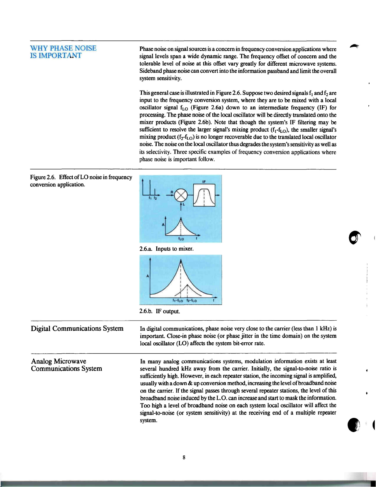
WHY PHASE NOISE
IS IMPORTANT
Phase noise on signal sources
signal levels span a wide dynamic range. The frequency offset of concern and the
tolerable level of noise at this offset vary greatly for different microwave systems.
Sideband phase
system sensitivity.
noise
is
a concern in frequency conversion applications where
can convert
into the
information passband and limit
the
overall
Figure
2.6.
Effect of LO noise
conversion application.
in
frequency
This general
input to the frequency conversion system, where they are to be mixed with a local
oscillator signal fLO (Figure 2.6a) down to an intermediate frequency (IF) for
processing. The phase noise of
mixer products (Figure 2.6b). Note that though the system's IF filtering may be
sufficient to resolve the larger signal's mixing product (fpfLo). the smaller signal's
mixing product (f2-fLo) is
noise.
its selectivity. Three specific examples of frequency conversion applications where
phase noise is important follow.
2.6.a. Inputs to mixer.
case is
illustrated in Figure
the
no
longer recoverable due to the translated local oscillator
The noise on the local oscillator thus degrades the system's sensitivity
2.6.
Suppose two desired signals f ] and f2 are
local oscillator will be directly translated onto the
as
well as
Digital Communications System
Analog Microwave
Communications System
2.6.b. IF output.
In digital communications, phase noise very close to the carrier (less than 1 kHz) is
important. Close-in phase noise (or phase jitter in the time domain) on the system
local oscillator (LO) affects the system bit-error rate.
In many analog communications systems, modulation information exists at least
several hundred kHz away from the carrier. Initially, the signal-to-noise ratio is
sufficiently high. However, in each repeater station, the incoming signal
usually with a down &
on the carrier. If the signal passes through several repeater stations, the level of this
broadband noise induced by the
Too high a level of broadband noise on each system local oscillator will affect the
signal-to-noise (or system sensitivity) at the receiving end of a multiple repeater
system.
up
conversion method, increasing the
L.O.
can increase and start to mask the information.
level
is
amplified,
of broadband noise
Page 10
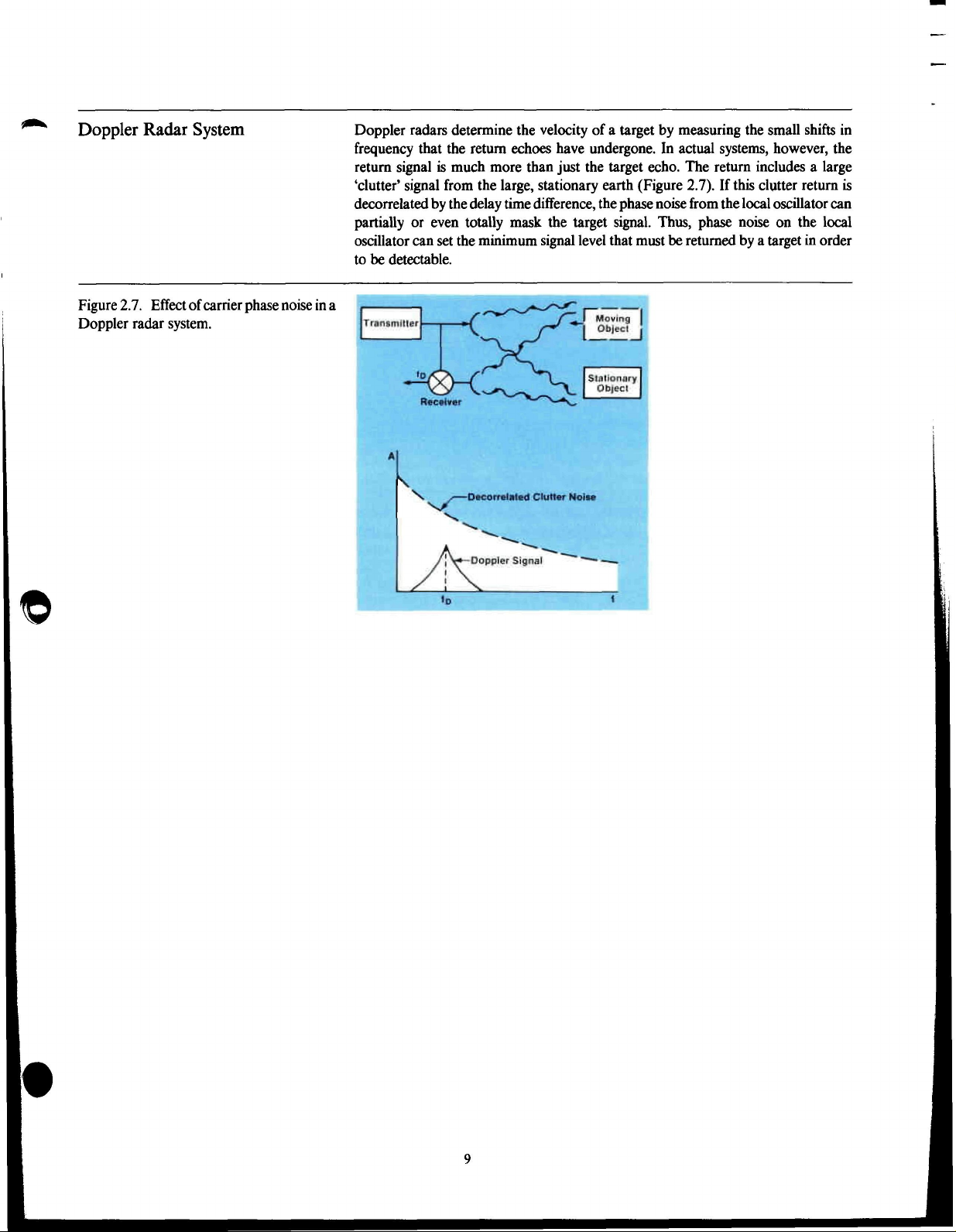
Doppler Radar System
Figure
2.7.
Effect of carrier phase noise
Doppler radar system.
Doppler radars determine the velocity of a target by measuring the small shifts in
frequency that the return echoes have undergone. In actual systems, however, the
return signal is much more than just the target echo. The return includes a large
'clutter' signal from the large, stationary earth (Figure 2.7). If this clutter return is
decorrelated by the delay time difference, the phase noise from
partially or even totally mask the target signal. Thus, phase noise on the local
oscillator can set the minimum signal level that must be returned by a target in order
to be detectable.
in i
the local
oscillator can
9
Page 11
3 Phase Noise Measurements—Frequency Discriminator Method
COMMON MEASUREMENT
TECHNIQUES
Direct Spectrum Measurement
Heterodyne/Counter Measurement
There
are several
of advantages and disadvantages. This brief summary of
methods also adds a few comments about their applicability.
The most straightforward method of
into a spectrum analyzer, directly measuring the power spectral density of the
oscillator. However, this method may be significantly limited by the spectrum
analyzer's dynamic range, resolution, and its own LO phase noise.
Though this direct measurement is not useful for measurements close-in to a drifting
carrier, it provides a convenient method for qualitative, quick evaluation on sources
with relatively high noise. The following conditions make the measurement valid:
A. the spectrum analyzer
the noise of the Device Under Test (DUT);
B.
since the
the DUT must be significantly below its own phase
suffice.)
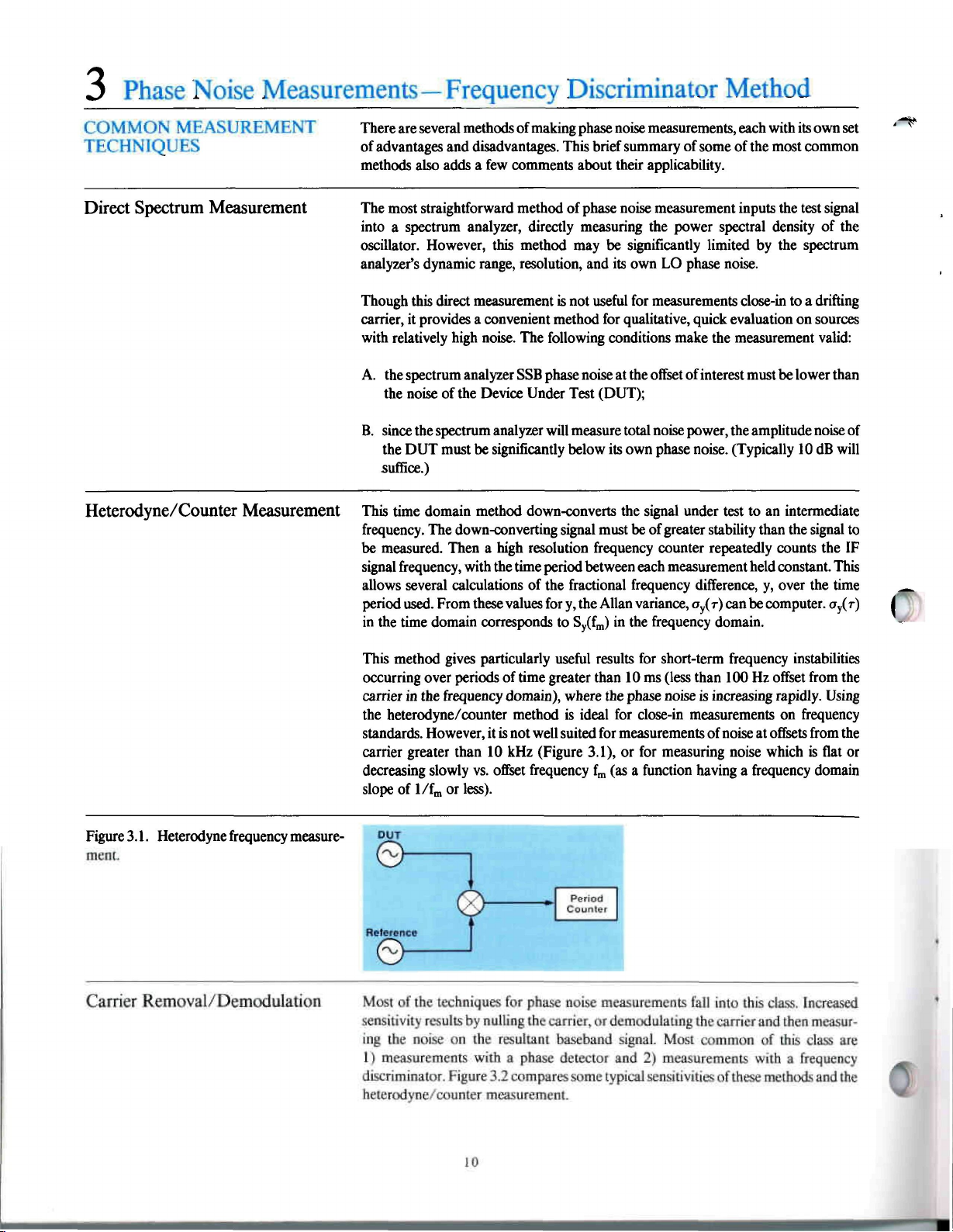
This time domain method down-converts the signal under test to an intermediate
frequency. The down-converting signal must be of greater stability than the signal to
be measured. Then a high resolution frequency counter repeatedly counts the IF
signal frequency, with the time period between each measurement held
allows several calculations of the fractional frequency difference, y, over the time
period
used.
in the time domain corresponds to
methods of making phase
SSB
phase noise at the offset of interest must
spectrum analyzer
From
these values
will
for
noise
measurements, each with
some
of
the
phase
noise measurement inputs the test signal
measure total noise power, the amphtude noise
noise.
(Typically 10 dB will
y,
the Allan variance, oy(r) can
Sy(fm)
in the frequency domain.
its
own set
most common
be
lower than
constant.
be
computer. ay(r)
of
This
Figure
3.1.
Heterodyne frequency measure-
ment.
Carrier Removal/Demodulation
This method gives particularly useful results for short-term frequency instabilities
occurring over periods of time greater than 10 ms (less than 100 Hz offset from the
carrier in the frequency domain), where the phase noise is increasing rapidly. Using
the heterodyne/counter method is ideal for close-in measurements on frequency
standards. However, it
carrier greater than 10 kHz (Figure 3.1), or for measuring noise which is flat or
decreasing slowly vs. offset frequency fm (as a function having a frequency domain
slope of l/fm or less).
DUT
is
not well suited for measurements of noise at offsets from the
©■
Mosi of the techniques for phase noise measurements fall into this class. Increased
sensitivity results
ing the noise on the resultant baseband signal. Most common of this class are
1) measurements with a phase detector and 2) measurements with a frequency
discriminator. Figure 3.2 compares
heterodyne/counter measurement.
by
nulling
the
carrier, or demodulating the carrier and then measur-
some
typical sensitivities of these methods and
the
It.)
Page 12
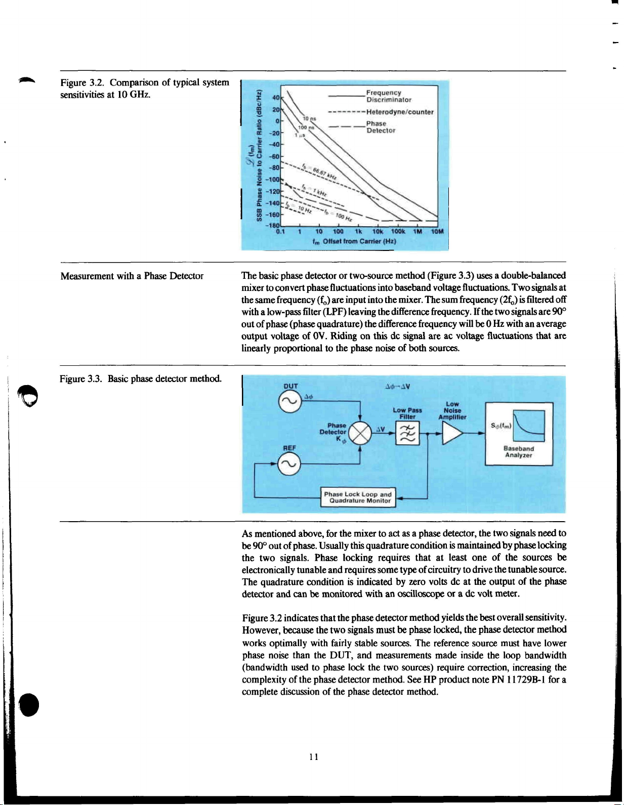
Figure 3.2. Comparison of typical system
sensitivities at 10 GHz.
10 100 Ik 10k 100k
tm Otlsalfrom Carrier (Hi)
Measurement with a Phase Detector
Figure 3.3. Basic phase detector method.
The basic phase detector or two-source method (Figure 3.3) uses a double-balanced
mixer
to
convert phase fluctuations
the same frequency (f0) are input into the
with a low-pass filter
(LPF)
out of phase (phase quadrature) the difference frequency will
output voltage of
0V.
Riding on this dc signal are ac voltage fluctuations that are
leaving
into
baseband
mixer.
the
difference frequency. If
voltage
The sum
fluctuations. Two
frequency
(2^)
the two signals
be 0 Hz
with an average
signals
is
filtered
at
off
are 90°
linearly proportional to the phase noise of both sources.
S,;,ffm}
Saieband
Analyzer
As mentioned above, for the mixer to act as a phase detector, the two signals need to
be 90°
out of
phase.
Usually
this
quadrature condition
is
maintained by
phase
locking
the two signals. Phase locking requires that at least one of the sources be
electronically tunable and requires some type of circuitry
to drive
the tunable source.
The quadrature condition is indicated by zero volts dc at the output of the phase
detector and can be monitored with an oscilloscope or a dc volt meter.
Figure 3.2 indicates that the phase detector method
yields
the best overall sensitivity.
However, because the two signals must be phase locked, the phase detector method
works optimally with fairly stable sources. The reference source must have lower
phase noise than the DUT, and measurements made inside the loop bandwidth
(bandwidth used to phase lock the two sources) require correction, increasing the
complexity of the phase detector method. See HP product note PN 11729B-1 for a
complete discussion of the phase detector method.
11
Page 13
Measurement with a Frequency
Discriminator
THE DELAY LINE/MIXER
FREQUENCY DISCRIMINATOR
METHOD
Basic Theory
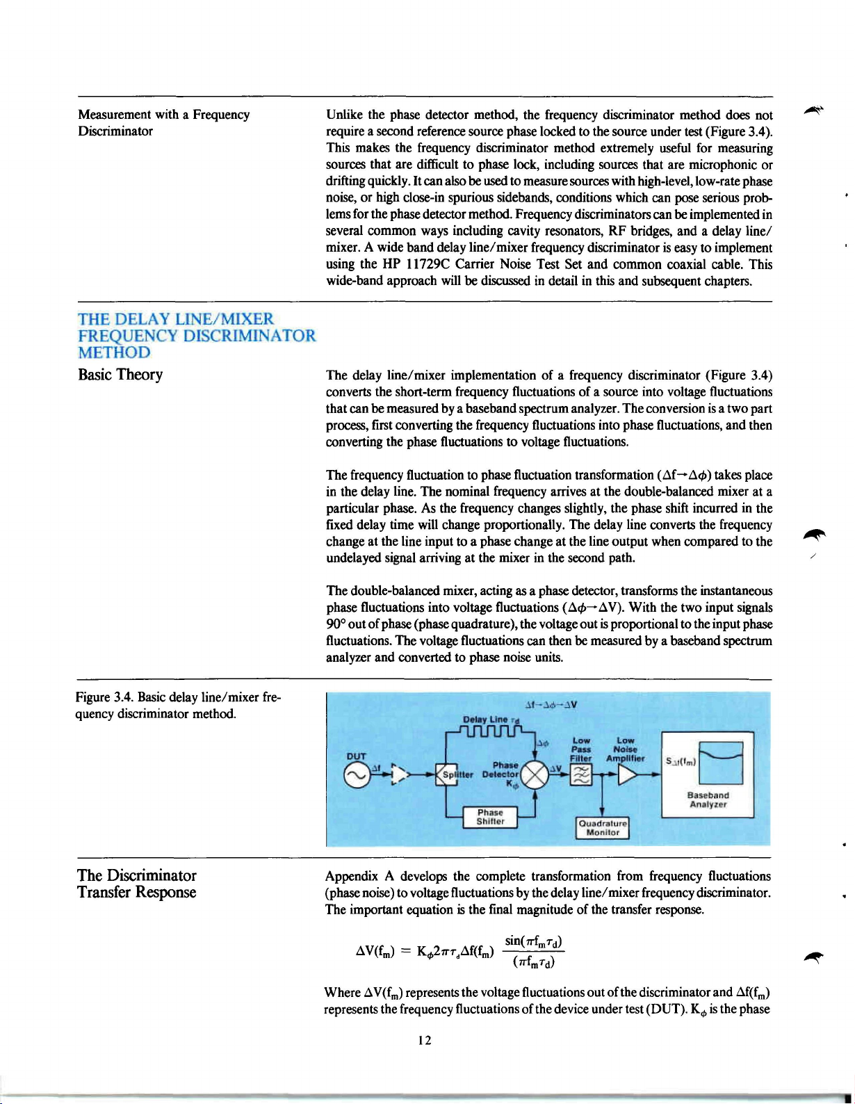
Unlike the phase detector method, the frequency discriminator method does not
require a second reference source phase locked to the source under test (Figure 3.4).
This makes the frequency discriminator method extremely useful for measuring
sources that are difficult to phase lock, including sources that are microphonic or
drifting
quickly.
It
can
also be
used to measure
sources
with
high-level,
low-rate phase
noise, or high close-in spurious sidebands, conditions which can pose serious problems
for the phase detector
method.
Frequency discriminators can
be
implemented in
several common ways including cavity resonators, RF bridges, and a delay line/
mixer. A wide band delay line/mixer frequency discriminator is easy to implement
using the HP 11729C Carrier Noise Test Set and common coaxial cable. This
wide-band approach will be discussed in detail in this and subsequent chapters.
The delay line/mixer implementation of a frequency discriminator (Figure 3.4)
converts the short-term frequency fluctuations of a source into voltage fluctuations
that can be measured
by a
baseband spectrum analyzer. The conversion
is
a two part
process, first converting the frequency fluctuations into phase fluctuations, and then
converting the phase fluctuations to voltage fluctuations.
The frequency fluctuation to phase fluctuation transformation (Af—-A<£) takes place
in the delay line. The nominal frequency arrives at the double-balanced mixer at a
particular phase. As the frequency changes slightly, the phase shift incurred in the
fixed delay time will change proportionally. The delay line converts the frequency
change at the line input to a phase change at the line output when compared to the
undelayed signal arriving at the mixer in the second path.
Figure 3.4. Basic delay line/mixer frequency discriminator method.
The Discriminator
Transfer Response
The double-balanced mixer, acting as a phase detector, transforms the instantaneous
phase fluctuations into voltage fluctuations (A#->AV). With the two input signals
90°
out of phase
(phase
quadrature),
the voltage out
is
proportional to the input phase
fluctuations. The voltage fluctuations can then be measured by a baseband spectrum
analyzer and converted to phase noise units.
DUT
KV,V*)
N—**SpHlltr
tuieclor
Phase
Shllter
Appendix A develops the complete transformation from frequency fluctuations
(phase
noise)
to voltage fluctuations by the delay line/mixer frequency discriminator.
The important equation is the final magnitude of the transfer response.
AV(fm) = K^27rrdAf(fm)
sin(7rfmrd)
Where AV(fm) represents the voltage fluctuations out of the discriminator and Af(fm)
represents the frequency fluctuations of the device under test
(DUT).
K^,
is
the phase
12
Page 14
detector constant (phase to voltage translation)
as
developed in Appendix
B.
rd is
the
amount of delay provided by the delay line and fm is the frequency offset from the
carrier that the phase noise measurement is made.
Ti
System Sensitivity
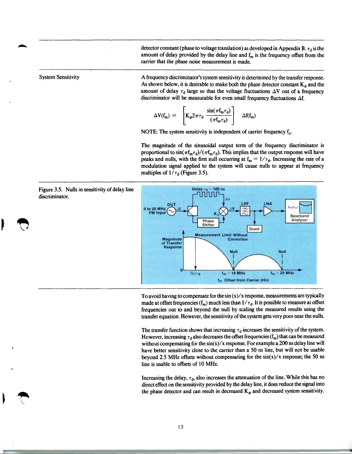
Figure 3.5. Nulls in sensitivity of delay line
discriminator.
A frequency discriminator's system sensitivity
is
determined by the transfer response.
As shown below, it is desirable to make both the phase detector constant K0 and the
amount of delay rd large so that the voltage fluctuations AV out of a frequency
discriminator will be measurable for even small frequency fluctuations Af.
sin(7rfmrd)
AV(fJ = K
27TT
0
d
(TrfmTd)
Af(fm)
NOTE: The system sensitivity is independent of carrier frequency f0.
The magnitude of the sinusoidal output term of the frequency discriminator is
proportional to sin(7rfmrd)/(7rfmrd). This implies that the output response will have
peaks and nulls, with the first null occurring at fm = l/rd. Increasing the rate of a
modulation signal applied to the system will cause nulls to appear at frequency
multiples of l/rd (Figure 3.5).
Delay rd lOOni
0
to
FM Input \
DUT
20 MH* /C\AJ
Magnitude
ol Trans lor
Response
Measurement Limit WMhoiil
Correction
Quad
"V
Q<-
ftirj-d lm " 10 MHz lm 20 MHi
t„.
OIIHI
Irom Carrier (Hi)
To
avoid having
made at offset frequencies (fm) much
to
compensate for
the sin
less
(x)/x
response,
than l/rd. It
measurements
is
possible to measure at offset
are
typically
frequencies out to and beyond the null by scaling the measured results using the
transfer
equation.
The transfer function shows that increasing rd increases the sensitivity of
However, increasing rd also decreases the
without compensating for the sin(x)/x
However, the sensitivity of the system
offset frequencies (fm) that can
response.
For example a 200
gets very
poor near
the
be
ns
delay
the
nulls.
system.
measured
line
will
have better sensitivity close to the carrier than a 50 ns line, but will not be usable
beyond 2.5 MHz offsets without compensating for the sin(x)/x response; the 50 ns
line is usable to offsets of 10 MHz.
Increasing the delay, rd, also increases the attenuation of the
direct effect on the sensitivity provided by the delay
line,
line.
While this has no
it
does
reduce the signal into
the phase detector and can result in decreased K^ and decreased system sensitivity.
13
Page 15

As developed in Appendix B the phase detector constant
mixer sine wave output at the zero
K^ equals KLVR where KL is
crossings.
When the mixer is not in compression,
the mixer efficiency and VR is
K^,
equals the slope of the
the voltage into the R port
of the mixer. VR is also the voltage available at the output of the delay line.
Optimum Sensitivity If measurements are made such that the offset frequency of interest (fm) is < 1 /2
the sin(x)/x term can be ignored and the transfer response can be reduced to
AV(fm) =
Y^M(fm)
= K*7rrdAf(fm)
where Kj is the discriminator constant.
The reduced transfer equation implies that a frequency discriminator's system sensi-
tivity can be increased simply by increasing the delay rd, or by increasing the phase
detector constant K^. This assumption is not completely correct. K^
is
dependent on
the signal level provided by the delay line and cannot exceed a device dependent
maximum. This maximum is achieved when the phase detector is operating in
compression. Increasing the delay Td will reduce the signal level out of the coaxial
delay line often reducing the sensitivity of the phase detector. Optimum system
sensitivity is obtained in a trade-off between delay and attenuation.
Appendix C develops this trade off in terms of coaxial delay line length L
Sensitivity = KLVinLXClO)-^
where KL is the phase detector efficiency,
20
V„,
is
the signal voltage into the delay line,
LX (dB) is the sensitivity provided by the delay line and LZ is the attenuation of the
delay
line.
Taking the derivative with respect to lenght L to
find
the maximum of this
equation results in
7rrd,
LZ = 8.7 dB of attenuation.
The optimum sensitivity for a system with the phase detector operating out of results
from using a length of coaxial line that has 8.7 dB of attenuation.
One way to increase
of compression is to increase the signal into the delay
with an RF amplifier before
degrade the measurement if the two-port noise of the amplifier
noise
of the
DUT.
local oscillator port of
the
sensitivity of
the signal
the
discriminator when the
splitter.
The noise of the RF amplifier will not
However, some attenuation may
the
double-balanced mixer (phase detector) to protect it from
phase
detector
line.
This can be accomplished
is
much
be
needed in the signal path
less
is
out
than the
to
the
excessive power levels.
If the amplified signal puts the
and system sensitivity
is
sensitivity more delay can be added until the signal level out of
phase
detector into compression, K^
now only dependent
is
at
its
maximum
on
the length of delay rd. For maximum
the
delay
line is
8.7
dB
below the phase detector compression point.
The following example illustrates how to choose a delay line that provides optimum
sensitivity given certain system parameters.
14
Page 16

Parameters
Source signal level
Mixer compression point
+7dBm
+3dBm
Delay line attenuation at
source carrier frequency
30dBper 100 ns of delay
Highest offset frequency
of interest
5 MHz
1) To avoid having to correct for the sin(x)/x response choose the delay such that
rd < . A delay rd of
2TT-5-W
32
ns or less can be used for offset frequencies
out to 5 MHz.
Making a Measurement
System Setup
Figure 3.6. Delay line/mixer frequency
discriminator.
2) The attenuation for
attenuation through the splitter and the delay line is 15.6
32 ns
of delay
is
30
dB-32
ns/100
ns
or 9.6
dB.
dB.
The signal level out
The total signal
of the delay line is —8.6 dBm which is 11.6 dB below the phase detector
compression point. Improved sensitivity can
the delay or by using a more efficient line
be
achieved by reducing
so
that the signal level out
the
length
is —5.7
of
dBm
or 8.7 dB below the mixer compression point.
Careful delay line selection is crucial for good system sensitivity. In cases where the
phase detector
lower
loss
is
operating out of compression, sensitivity can be increased by using
delay
line,
or
by
amplifying the signal from the
DUT.
Because attenuation
a
in coaxial lines is frequency dependent, optimum system sensitivity will be achieved
with different lengths of
Making a phase noise measurement with the delay line/mixer implementation of
frequency discriminator can
line
for different carrier frequencies.
be
broken into
3 simple
steps:
1)
system
setup;
2)
a
system
calibration; and 3) noise measurement.
Figure 3.6 shows a delay line/mixer frequency discriminator implementation. Details
to check during the setup are the signal level out of
the
delay line and the ability to
obtain quadrature. If the level is more than 8.7 dB below the phase detector
compression point delay line attenuation
is
too great and maximum sensitivity is not
being achieved.
Delay Llna.'d
Low
Nolle
DUT Amplifier
©HL^HS
Low Low
PHI
Noise
Fitter Amplifier
■|>~
Sjltlm)
Baleband
Analyzef
System Calibration
The calibration procedure determines the discriminator constant Kd to use in the
transfer response .iV = KjAf =
K^ and ru individually, and 2) measuring
K^,2TTTJ
Af. Kj can be determined by )) measuring
the
overall Kd by measuring the response
of
the system lo a known input.
The delay
r^
is a
function of both the length and type of delay line used. For example,
for coaxial cables with a polyethelcne dielectric the delay is approximately 1.5
15
Page 17

ns/foot. An accurate measure of the delay can be made by setting up a delay line
discriminator and varying the input signal carrier frequency through two zero
crossings on the quadrature monitor (an oscilloscope or dc volt
will equal 1/(2 Af0) where Af0 is the change in the carrier frequency needed to pass
through the two consecutive quadrature points.
meter).
The delay r
d
Figure 3.7. Carrier with single FM tone.
K^ the phase detector constant
phase detector as indicated in Appendix
generate the beat note. The signal level of the second source must match the signal
level out of the delay line for accurate calibration.
Usually the easiest way to determine the discriminator constant Kd is by measuring
the system response to a known FM signal. The signal depicted in Figure 3.7
represents a carrier with
rad, the power in the higher order sidebands is negligible. Note the system must be
operating in quadrature during calibration.
equation as developed in Appendix D.
Kd [dB] = P^ [dB] - (ASB^ [dBc/Hz] + 20 tog^ [dBHz] + 3 [dB])
Pcai is
the system
analyzer.
the rate of the FM signal.
1
zl
d-
w
fT
V~
ASB^,
/
/
/
/
/
response to
is
the
\
t
\
/
/
(
\j
V
first
can be
determined
B.
a single
\
\
-■m
FM
tone.
If the modulation index
the known FM signal and
sideband
\
\
\
V
cil"*"
to
carrier ratio of the calibration signal and f^ is
AS
tell
/
r^
/
\
/
\
\
%
j
T
!F
by
developing a beat
This method requires a second source to
K<j [dB]
is calculated from the following
is
measured with the spectrum
note
/? is
kept below 0.2
out of the
The Phase Noise Measurement
Ctnlw 5110.000 MHi SPAN 5.00 kHz
Once Kd [dB] is determined it can be used to convert the detected output of the
discriminator
source
in a 1 Hz bandwidth. Since K
rithmic form
SJtJ [dBHz/Hz] =
Since phase noise
must be converted to 1 Hz noise bandwidth data. This is a simple power normalization process, where the noise bandwidth correction, NBW(dB), is simply
Sv(fm)
[dB] into the spectral density of frequency fluctuations of the
SAf(fm)
[dBHz/Hz] (source phase noise). By definition
is
typically defined for
NBW [dB] = 10 log
16
2
=
d
Sv(fm)
[dBm] - Kd [dBm]
B„
1Hz
SAf(fm)
AV2 AV
AP
a 1 Hz
,then SAf =
n
bandwidth, the measured
= AP
or in loga-
2
noise
rms(fm
power
2
K,
)
Page 18

where Bm is the actual measurement bandwidth.
The correction NBW [dB] is subtracted from the measured data to convert the
measured phase noise to a 1 Hz noise bandwidth. The power spectral density of
frequency fluctuations is then given by
SAf(fm)
[dBHz/Hz] =
Sv(fm)
- Kd - NBW
or, using the relations developed in Chapter 2, the power spectral density of phase
fluctuations is given by
S<»(fm) [dBr/Hz] =
Sv(fm)
- Kd - NBW - 20
logf
m
For peak phase deviations «1 radian, the single sideband phase noise to carrier
ratio is given by,
^(fm) [dBc/Hz] =
Sv(fm)
- Kd - NBW - 20
logfm - 3 dB.
For HP analog spectrum analyzers the noise bandwidth is 10 log (1.2-RBW) where
RWB is the resolution bandwidth indicated on the front panel.
T
i
Page 19

4 HP 11729C Theory of Operation and Measurement Considerations
The HP 11729C Carrier Noise Test Set implements the delay line/mixer frequency
discriminator for phase noise measurement on sources from 10 MHz to 18 GHz. It
can also be used for the phase detector method (see HP Product Note PN 11729B-1,
HP Lit. #5952-8286). This chapter explains how the HP 11729C makes measurements using
sensitivity of better than —140 dBc/Hz at a 1 MHz offset from a 10 GHz source.
the
delay line/mixer frequency discriminator and provides typical system
GENERAL OPERATION
Figure 4.1. HP 11729C simplified block
diagram.
The HP 11729C Carrier Noise Test Set uses an internal low noise microwave
reference signal to down-convert the test signal to an IF frequency. The resulting IF
signal is amplified and then applied to a delay line/mixer frequency discriminator
where the phase noise is demodulated and made available for analysis.
The HP 11729C supplies everything needed for a delay line discriminator measurement except the delay line and the spectrum analyzer. The Carrier Noise Test Set
includes the phase detector, the quadrature monitor, and both the low noise IF and
baseband amplifiers. Because the discriminator operates at an IF frequency below
1.28
GHz,
common coaxial cable such
because the output of the discriminator is amplified, almost any available low
frequency spectrum analyzer can be used. The HP 11729C provides all this in a
compact package that is HP-IB controllable, making automatic phase noise measurements easy.
The HP 11729C features a major new contribution with its improved low noise
microwave signal needed for the down conversion to the IF frequency. Remember
from Chapter 2 that the noise on this reference signal
on the
IF
signal.
This means that the signal used for down-conversion must have very
low phase noise or its noise will mask the noise of the source under test. The
generation of this signal leads to the first n of the HP 11729C. See Figure 4.1 for a
simplified block diagram of the HP 11729C. For a more complete block diagram see
Figure 4.4.
DUT
r
Demodulation and Baseband Signal Processing
as
RG223 can be used for the delay
is
down-converted and appears
~\
line.
Also
MULTIPLIER CHAIN
0
10MHI-
leGHi
MO
I
To obtain a low noise microwave signal, the HP 11729C requires a fixed frequency
640 MHz drive signal for multiplication to microwave.
There are two ways to obtain the 640 MHz signal. One is to use the auxiliary 640
MHz fixed frequency output of the HP 8662/8663 Synthesized Signal Generator.
I
r
■-T!
i L
I
I
I
{>-
$
**>
i_'_ _-rr_ i
Multiplier Chain
18
Oulpu
£Ln_nj-|_r
Out
i |j
i
i
i
i
Guides lure
Section
5-128Q MHz
J
Input
Page 20

Figure 4.2. HP 11729C cable hookup for
640 MHz self-generation.
(The HP 8662/8663 are used with the HP 11729C to make phase noise measurements using the phase detector method, see PN 11729B-1.) If an HP 8662/8663 is
part of the measurement system, the auxiliary 640 MHz output is an excellent low
noise drive signal for the HP 11729C.
However, for a low-cost, stand-alone system, the HP 11729C can be configured to
generate its own 640 MHz signal internally. A Surface Acoustic Wave (SAW)
oscillator can be created
two rear panel connectors of
Figure 4.2. (Do not substitute cables as the physical length affects the oscillating
frequency.)
The 640 MHz reference signal determines the HP 11729C system noise floor. Figure
4.3 shows the noise floor of the HP 11729C at 10 GHz when in the SAW oscillator
mode or when using the signal from the HP
the SAW oscillator mode is lower from 70 kHz to 10 MHz, and the noise floor
provided by the HP 8662/8663 is lower from 70 kHz and closer.
by
connecting the 640 MHz output to the 640 MHz input on
the
HP 11729C with the included cable as indicated in
8662/8663.
Note that the noise
floor
for
I
Z>
I 9
Figure 4.3. Noise floor of HP 11729C
phase noise test system.
i
s
I
s
I
\
I
i
9C «<ih HP
s
i
1
i
The standard HP 11729C uses 8 microwave transfer switches with 7 bandpass filters
installed (Figure
GHz and to switch from band-to-band under computer control for automatic testing.
For test frequencies less than 1.28 GHz, one switch bypasses the microwave mixer
and applies the test signal directly to the IF amplifier. A single filter version of the HP
11729C, for narrowband or single test frequency applications, retains the bypass
switch for low frequencies and one user-defined bandpass filter, at lower cost.
HP 1173
-1IO
-140
160
rt* 10 Hi 1WH1 1*HI m*H* 1M
iflO MHi jil
1
4.4).
\
\
\
j'Otclllitnj
\
">f ll
10
GHl
OGHl
t„ OttHl Worn
This allows it to down-convert test signals from
C*rri*r
■H
%
(Hi)
^
s^_
^***>
"""^
VKJ 1MKI
—
10
HHi
10
MHz to 18
19
Page 21

DEMODULATING AND
BANDPASS SIGNAL
PROCESSING SECTION
Once the HP 11729C
DUT frequency, the microwave test signal is down-converted and processed.
has
generated the very low
noise signal
within
1280 MHz
of the
First Down-conversion The selected harmonic of the 640 MHz
(Microwave mixer) under test in the input mixer, yielding an IF frequency between 10 to 1280 MHz.
Because of
test must provide the local oscillator (LO) drive
and +20 dBm (for input signals >1.28 GHz) is appropriate. For DUT frequencies
between 10 MHz and 1.28 GHz, the signal is input directly into the IF amplifier and
should have a signal level of between —5 and +10 dBm.
IF Processing and the The resultant IF signal is amplified and then split into two paths. One of the signals
Frequency Discriminator supplies
the phase detector. The other signal
monitoring or in this case to be connected to the external delay line. After passing
through the delay line, the signal returns to the R port of the RF mixer (5 to 1280
MHz input).
Typical values of
dBm, depending on the IF frequency. The minimum specified value for
dBm. A high level IF signal is important as it allows the use of longer delay lines for
improved sensitivity.
The resultant IF signal phase correlates against a delayed version of
signals are 90° out-of-phase (phase quadrature), the RF mixer operates
phase detector. If
ing baseband signal represents the frequency noise of the microwave test source.
the
low signal level of
the local
oscillator drive to the RF double-balanced mixer that
the
the
IF signal level out of
frequency discriminator has the required sensitivity, the result-
drive
signal mixes with the microwave source
the
higher frequency comb
power.
is
output to the front panel of the HP 11729C for
the
front panel are between +9 and +14
lines,
the source under
A signal level of between +7
will be
all
IF
itself.
If
as
the system
used as
es is
the
two
+7
Baseband Signal Processing A 15 MHz (3 dB BW) Low-Pass Filter (LPF) processes the baseband signal to
remove the mixer sum products and the LO feedthrough. The baseband signal is
further processed through a Low Noise Amplifier (LNA), and then applied to the
<10 MHz Noise Spectrum Output for viewing with a spectrum analyzer.
The amplifier
of about 10 Hz to 30 MHz. Typical flatness is less than 1 dB and the noise
<2.0
dB.
standard lab spectrum analyzer at the <I0 MHz output.
If the IF frequency is less than 20 MHz, additional low-pass filtering is needed to
remove the unwanted mixer products and LO feedthrough. The HP 11729C provides
a L5 MHz low-pass filler thai allows IF frequencies of 10 MHz or greater to be
processed. The resulting noise signal is available at the <1 MHz Noise Spectrum
Output for viewing on a low frequency spectrum analyzer. The < I MHz
amplified by the LNA. If a lower IF Frequency
can be user added.
The IF amplifier of
problem as the comb line fitters are chosen such that the IF frequency is never more
than 1280 MHz. For example the 9.6 GHz filter covers test frequencies from 8.32
GHz to 10.88 GHz (excluding ±
has
approximately 40
The LNA permits the HP 11729C detected noise output to be viewed on a
the
HP 11729C
:n
dB
of gain (coupled into 50O
is
critical,
is
bandwidth limited to 1500 MHz. This
10 MHz
centered on 9.6
additional low-pass filtering
GHz).
I,
and a bandwidth
figure
signal is
The frequency of the
is
not
not a
is
Page 22

Figure 4.4. HP 11729C Carrier Noise Test
Set.
selected comb line, as well as the range of input signals that can be down-converted
with each comb line, are indicated on the front panel of the HP 11729C.
OUT
AM Hoar Option
■""1
&><>J
J^>_(^
OomotfuteMan A Signal Protesting
Pufxd
Baseband
11
Output
. i
Input
Ourtdraturr
Indicator
Spectrum
Outputs
■*■ tOMHtSO!!
-»-•
1 MHz 600i
-*- AVX 600 It
i
PHASE-LOCK LOOP/
QUADRATURE SECTION
LqjpJ
The inputs to the
phase
S-ISBOMHi
Input
detector must
be
maintained
in
quadrature for the duration of
the measurement. Quadrature can be observed on the red and green LED display of
the front panel of the HP 11729C or can be monitored over the HP-IB bus during
automated
measurements.
The
phase-lock
loop
circuitry
is
not used when implementing the frequency discriminator because the DUT signal is phase detected against
itself.
However the quadrature indicator remains active and can
be
used to insure that
quadrature is maintained.
21
Page 23

J Making Frequency (Phase) Noise Measurements with
This chapter integrates the theory of the delay line/mixer frequency discriminator
(Chapter 3) and its implementation in the HP 11729C (Chapter 4) into procedures
for making phase noise measurements on microwave sources. The measurement
procedure breaks down into three easy
and 3) noise measurement. Specific instrument operation instructions are given for
the HP 11729C Carrier Noise Test Set.
steps:
1)
system
the
HP11729C
set-up;
2) system calibration,
SYSTEM SET-UP
Figure 5.1. System set-up for making a
delay line/mixer frequency discrimination
phase noise measurement.
The Source
The delay line/mixer implementation of a frequency discriminator with the HP
11729C is shown in Figure
required to obtain quadrature if the source frequency
5.1.
Note that a phase shifter or a line stretcher may be
is
not adjustable. The maximum
frequency adjustment Af„ required of the source can be determined from the follow-
ing equation
Af0 =
l/4r
d
MO MH*
Horn
_t 1
r
I HP 8662/3 I
I I
Microwave
Ts»t
G>
IOMHl-18 GHl
The frequency of
Microwavn Tell
Signal In
the
test source determines the filter band of
eao MHz Out
HP11729C
MOMHi
C
-.5-1280 MH*
In
1OMH1
Out
H=
Spectrum
Anilywr
the
HP 11729C to be
used. Because the source must provide the local oscillator drive signal (LO) to the
microwave mixer for frequencies above 1.28
GHz,
the source output power should be
between +7 dBm and +20 dBm. For frequencies below 1.28 GHz the microwave
mixer
is
bypassed and
dBm (with an optimal
the source
level
from
output power should
—2
to +3
dBm).
Power
be
between — 5 dBm and +10
levels
below +7 dBm (—5
dBm <1.28 GHz) can be used with a degradation in the system noise floor. Keep the
cable length from the source under test to the HP 11729C short to reduce cable
attenuation. This will help provide the necessary LO level and also help prevent
system noise floor degradation.
The 640 MHz Drive Signal
The 640 MHz drive signal required by the HP 11729C can be self-generated or
obtained from an HP 8662/8663 Synthesized Signal Generator. By using the self
generated 640 MHz drive
signal, a lower system noise floor results from 70 kHz to 10
MHz. (Typically the phase detector method is used if close-in sensitivity is needed.
See HP product note PN 11729B-1 Phase Noise Characterization of Microwave
Sources—Phase Detector Method.) To use the self-generated 640 MHz drive signal,
connect the supplied cable between the rear panel 640 MHz output and 640 MHz
input
ports.
To
use
the 640 MHz drive signal from an HP 8662/8663 connect
MHz output from the rear of
rear panel of the HP
11729C.
the
HP 8662/8663 to the 640 MHz input port on the
Then
cap
the
640
MHz output port on the HP 11729C
the
640
with the 50O SMA termination provided.
22
Page 24

<?~>,
The Delay Line
As developed in Chapter 3, system sensitivity depends on both the length and
attenuation of the delay
signal to
or semi-rigid
an
IF
cable.
frequency of
line.
Because the HP 11729C down-converts the microwave
less
than 1.28
Coaxial cable such
as
GHz,
RG
the delay
223
line
provides about 1.5
can
be
common coaxial
ns
delay per foot
of cable.
Because a discriminator is typically used only to offsets of less than 1/2 rd, the
maximum delay to be used is determined by the highest offset frequency of interest.
For example, if measurements are desired of an offset frequency (fm) of
delay must be less than 1/2 fm =
1/2(10
MHz) = 50 ns.
10
MHz,
the
n
Figure 5.2. Optimum system sensitivity/
delay line length vs. IF frequency.
An easy way to determine the delay r for an unknown length of
cable is
to tune the
source frequency so that phase quadrature occurs, then continue tuning the source
until quadrature is again established. The delay rd is equal to l/2(Af0) where Af0 is
the frequency difference between the two quadrature points.
After choosing a cable length, measure the signal power out of the HP 11729C IF
output through the length of cable with a spectrum analyzer. As developed in
Appendix C, optimum sensitivity results if the power out of the delay is approximately
—5
dBm. If
too great and system sensitivity
the
power out goes below
degrades.
—5
dBm, the delay line attenuation is
Either use a delay line with
less
attenuation
or shorten the delay line until the signal power equals —5 dBm. This increases the
system sensitivity and also increases the offset frequency to which measurements can
be made without corrections to the discriminator transfer response.
Because cable
by reducing the IF frequency out of
attenuation
is
frequency dependent, system sensitivity
the
HP 11729C. This technique is only possible
can be
improved
by tuning the source under test. The reduction of delay line attenuation translates
directly into increased system sensitivity. Figure 5.2 shows typical lengths of RG 223
coaxial cable versus HP 11729C IF frequencies that provide optimum sensitivity.
Figure 5.3 shows the sensitivity of the HP 11729C implementation of the delay line
frequency discriminator using a 100 ns RG 223 delay line.
x
400
E
• 300
il
o
gaoo
a
E
100
\
\
\
\
-HP11729C
—-
1P1172S
a\
+7
dB
m
0
200 400 GOO 800 1000 1200
HP 117Z9C IF Frequency (MHl)
OG 223 Cable used as delay lino
°-~i
1
450
f
300 «
a
_
'
150
f)
23
Page 25

Figure
5.3.
Typical HP 11729C sensitivity
with a 100 ns delay line.
SSa Phase Noise
to Carrier Hallo
^■(WldBe/Hi] -100
-120
-160
,SAW
Oscillator
•V~at10GHi
HP 11729C with HP B662/3
S40MHia110GHz
1Hz 10Hz 100Hz 1kHz 10kHz 100kHz 1MHz 10
L Oflsel Irorn Carrier (Hi)
MHz
System Operation
SYSTEM CALIBRATION
The Calibration Signal
Make the following tests to insure that the HP 11729C system is operating as
expected. Disconnect the delay line from the IF output port on the HP 11729C and
measure the IF frequency and the IF power with an RF spectrum analyzer. The IF
frequency should be equal to the source under test frequency minus the filter center
frequency.
IF= f(source) - f(filter)
The IF output power should
signal is obtained, reconnect the delay line between the IF output and the
MHz input ports on the HP 11729C. Check to
be
greater than or equal to +7
see
that quadrature can
dBm.
After
the
proper IF
5-1280
be
established
by adjusting the source frequency, the phase shifter or the line stretcher. The green
LED in the PHASE LOCK display on the HP 11729C front panel indicates phase
quadrature. After obtaining quadrature the system is ready to be calibrated.
Usually the easiest way to calibrate the frequency discriminator is to measure the
system response to a known signal. This establishes a reference for subsequent
measurements. System calibration consists of the following:
a) generation and measurement of the calibration signal.
b) measuring system response to the calibration signal.
c) calculating the discriminator constant Kj.
A
signal with a single FM tone will be used
under test itself can be modulated to produce
as
the calibration
this
signal.
signal.
Often the source
If not, an alternate source can
be substituted for the test source. The substitution method can be made either with a
microwave source or at the IF frequency (see Figures 5.4 and 5.5).
f*
Figure 5.4. Calibrating the HP 11729C
delay line/mixer frequency discriminator
with a microwave source.
Microwave
Carrier
with known
FM
Modulation
1,28-18
GHz T
r
Filter Band
I Filler tsa
_(2-<M
24
IF Output
5-12S0
IF
AMP
MH2
Delay
Lin*
5-1280
] Input
MH*
HP11723C
System
Response
c
Page 26

Figure 5.5. Calibrating the HP 11729C
delay line/mixer frequency discriminator
with an RF source.
OF Carrier
with known
FM
Modulation
IF Oulpul
5-12SD MHi
IF
AMP
Daisy Line
Pcil
t
M2S0MHII I I
Filler Bund
(11
System
Retponi*
The modulation index on the calibration signal should be set to <0.2 radians (to
satisfy the small angle criterion and the relation between
SAf(fm)
and =^(fm) as
developed in Chapter 2). The modulation index /? is the peak FM deviation (Afpk)
divided by the FM rate (fm).
Af,
k
P = modulation index = —
P
Remember:
^(fm) =
sAf(fm)
2P
m
2P
(for m <0.2 rad)
m
An FM rate of 1 kHz with a peak deviation of 0.1 kHz yields a modulation index of
0.1 radian which should result in a sideband to carrier ratio of
—26
dBc.
Record the
FM rate used in the calibration signal (f,^ = ). See Appendix D for a more
complete discussion of the calibration theory.
If the source under test cannot be modulated, the system can still be calibrated by
substituting a modulated microwave source at the same level and frequency. The HP
8683/8684 Signal Generator and the HP 8672/8673 Synthesized Signal Generator
are all good microwave sources that could be used.
System Response
If a modulated microwave source is not available, then calibration can still be
accomplished
by
using a modulated RF
source
substituted at
the
IF frequency. Set the
RF calibration source to the HP 11729C IF frequency, at a level of—10 dBm with
FM modulation applied (/3 <0.2 radians). Setting the signal level to —10 dBm
improves the calibration accuracy by closely matching the signal level of
converted microwave test
signal.
A signal level between
—3
and +2 dBm gives best
the
down-
results for test sources that use the <1280 MHz filter band directly. The HP
8662/8663,
8640, 8642, 8656, and 8660 all have internal modulation capabilities
and can be used as the RF calibration source.
Measure the sideband to carrier level of the calibration signal with a spectrum
analyzer, and record this ratio (ASB,^ = — dBc).
The second step in calibrating the system measures its response to the signal created
previously. Connect
the HP 11729C and select
the 0.01-1.28 GHz
indicates phase quadrature by
the
calibration signal to the Microwave Test Signal input port on
the
appropriate filter
band.
Before measuring the response, check to
the
green LED in the Phase Lock Indicator on the front
band.
If RF calibration
is
used, select
see
that the system
panel of the HP 11729C. Set auadrature bv adjusting the calibration source fre-
quency, adjusting the phase shifter, or adjusting the line stretcher.
25
Page 27

Once quadrature has been obtained, measure the system response to the calibration
signal.
The demodulated calibration signal will have
frequency corresponding to the FM
the power
so
that the spike
help improve measurement accuracy, by avoiding extra corrections for display
attenuation steps.
level,
P^ = If possible, adjust
is
at
the top
of the
rate,
as
display.
shown in Figure
Leave the input sensitivity at
a sharp
response at
5.6.
the
spectrum analyzer input sensitivity
the
baseband
Measure and record
this setting
to
Figure 5.6.
signal.
System response to calibration
r
P
JS
"l
T
4
\
* nicai "*
BHi Frequency Hi 5,00
Discriminator Constant (Kd)
MEASURING THE FREQUENCY After completing calibration, the source frequency noise can be measured by:
(rHAab) NUlbt
a
To complete the calibration procedure, calculate the discriminator constant Kd. As
explained in Appendix D,
K<j
[dBm] = P^ [dBm] - [3 dB + 20 log ^ + ASB^]
Calculate and record the discriminator constant.
Kd [dBm] =
) Measuring the frequency noise.
b) Applying measurement corrections.
c) Converting to other phase noise units if desired.
™
(LHJ
Measuring the Frequency Noise
If an alternate source was used for calibration, reconnect the test source to the HP
11729C Microwave Test Signal input. If an RF source was used, select the appropriate filter band on the HP 11729C
itself
was
used for calibration, remove the FM modulation from it. Adjust the source
frequency, phase shifter, or line stretcher as necessary to re-establish phase quadrature.
Quadrature should be maintained throughout the measurement procedure.
Set
up
the spectrum analyzer span
sensitivity of the spectrum analyzer should not be changed from the calibration
procedure if possible. Select a resolution bandwidth RBW that
chosen frequency
10 kHz to 100 kHz, or 10 kHz for 100 kHz to 10 MHz.
Because noise
digital averaging can be selected or some analog averaging can be done by reducing
the video BW on the spectrum analyzer. The HP 8566 Spectrum Analyzer
suited.
span.
For
example, a good choice of RBW is 1 kHz
is
a random quantity, some sort of averaging
26
to
down-con ven the test
to
cover the offset frequencies of interest. The input
source.
If the test source
is
in keeping with the
for
a span from
is
desirable. If available,
is
ideally
Page 28

After averaging, take a reading from the spectrum analyzer in dBm at the offset
frequency of interest, noting the resolution bandwidth setting. Set other frequency
spans and make measurements as desired. Record the values from the spectrum
analyzer display (Pnoise)>
tne
offset frequencies they were taken at (fm), and the
resolution bandwidths (RBW) used to measure the value.
P
= [dBm] fm [Hz] RBW = [Hz]
noise
Noise levels measured within 10 dB of
can degrade the measurement accuracy. If
the
bottom of the spectrum analyzer's display
possible,
increase the spectrum analyzer
input sensitivity and repeat the measurement. This should not be a problem if the
calibration signal P^i
is
brought to the top of
the
CRT as discussed in the calibration
procedure.
Measurement Corrections Because the spectrum analyzer responds differently to sine waves than to random
noise, two corrections must be made to the measured data. The first correction
accounts for the log-shaping and detection circuitry of
an
analog spectrum analyzer.
This correction (SA) is +2.5 dB for HP analog spectrum analyzers (see HP applica-
tion note AN 150-4).
The second correction normalizes the measurement to a 1 Hz noise bandwidth
(NBW) and accounts for the spectrum analyzer resolution bandwidth used during
the noise measurements. This correction (NBW) is 10 log (1.2 • RBW) to the first
approximation for HP spectrum analyzers, where RBW is the indicated resolution
bandwidth on the analyzer.
As developed in Chapter 3,
SAf(fm)
equals the spectrum analyzer display Pnoise(fm)
minus the discriminator constant Kd. Including the measurement corrections to the
original equation yields:
SAf(fm)
[dBHz/Hz] = P
(fJ [dBm] - Kd [dBm] + SA [dB] - NBW [dB]
noise
where from Appendix D
IC [dBm] = P,*, [dBm] - (ASB^, + 20 log L . + 3) [dB].
Conversion to Other Units To convert
Chapter 2 and the two previous equations. J^(fm) and
£({J [dBc/Hz] =
P
noise
[dBm]
- P^,
[dBm]
+ ASBcal
= SAKfm)-201ogfm-3dB
S^(fm)
[dBr/Hz] =
P
[dBm] - P^, [dBm] + ASB^, [dBc] - 20logy12— NBW [dB] + SA [dB] + 3 dB
noise
=
SAf(fm)-201ogf
m
Figures 5.7, 5.8, and 5.9 show example calculations required to obtain SAf(fm),
S^d'n,},
and J (fm) using data from a free running
I kHz tone (fm ,) with a modulation index of 0.2 rad (ASBCB] = — 20 dBc). The
system response P^i was
MHz offset was —71.5 dBm. The resolution bandwidth (RBW) of the spectrum
analyzer used during the measurement was 300
ently different represents the phase noise for the same VCO expressed in different
units.
SAf(fm)
[dBc]
to other phase noise units, use the relationships developed in
S,j(fm)
can be derived as
f
- 20
27
m
log
-z NBW [dB] + SA [dB]
■"cal
m
cal
VCO.
—54.6 dBm
and the
lest source
H/..
Calibration
frequency
was
made with a
noise (P
nulM
.) ai a 1
Note each result though appar-
Page 29

Figure 5.7. Computing
SAf(fm)
[dBHz/Hz] 1) Establish known sideband/carrier ratio
from the spectrum analyzer display.
2) Record
f
mca|
f
mcal
ASB^fJ = -20 dBc
=lkHz
Figure 5.8. Computing
S^(fm)
[dBr/Hz] 1) Establish known sideband/carrier ratio
from the spectrum analyzer display.
3) Measure system response
4) Determine discriminator constant
Kd[dBm] = P^tdBm] - (ASB^,^20 log f
5) Measure
P
(in known RBW)
noise
mcal
6) Noise Bandwidth correction
NBW [dB] = 10 log RBW • 1.2
7) Spectrum Analyzer correction
8) SAf (UtdB] = (P
noise
-
Kd +
S/R - NBW)
SAf (U[dB] = (-71.5) - (-97.6) + 2.5 - 25.5
2) Record
f
,
^
mca
L
1 kHz
3) Measure system response
4) Measure Pnoise (m known RBW)
5) Offset frequency
Wse, = 1
MHZ
6.) Noise Bandwidth correction
NBW [dB] = 10 log RBW • 1.2
Pcai = "54.6 dBm
+3)[dB] Kd =
Pnoise = -71.5 dBm
NBW = 25.5 dBHz
S/A = 2.5 dB*
SAftfm) = 3.1 dBHz/Hz**
ASBcal(fm) = -20 dBc
Peal = -54.6 dBm
Pnoise = -71.5 dBm
NBW = 25.5 dBHz
-97.6 dBm
7) Spectrum Analyzer correction
8) S^fJ = Pn0iSe - Peal + ASB^i - 20 log
(-71.5) - (-54.6) + (-20) - 20 log IPL - 25.5 + 2.5 +3
Figure 5.9. Computing i?(fm) [dBc/Hz] 1) Establish known sideband/carrier ratio
from the spectrum analyzer display.
2) Record
f
,
mca
f
,= lkHz
mca
3) Measure system response
4) Measure Pnoise (m known RBW)
5) Offset frequency
f
=
m
1 MHz
6) Noise Bandwidth correction
NBW [dB] = 10 log RBW • 1.2
7) Spectrum Analyzer correction
8) S£(tJ = Pnoise " Peal + ASB^i - 20 log^
(-71.5) - (-54.6) + (-20) - 20 log 15L- 25.5 + 2.5
S/A = 2.5 dB*
f,
■"offset
103
S0(fm) = -116.9 dBr/Hz**
- NBW + S/A + 3 dB
m
cal
ASB^fJ = -20 dBc
Peal = -54.6 dBm
Pnoise = -71-5 dBm
NBW = 25.5 dBHz
S/A = 2.5 dB*
m
offset
- NBW + S/A
m
cal
103
i?(fm) = -119.9 dBc/Hz**
♦Correction for HP analog spectrum analyzers.
**Phase noise measured at a 1 MHz offset from the carrier.
28
Page 30

O Considerations in System Accuracy
After configuring a phase noise measurement system, it may be necessary to determine the accuracy of
that can affect overall system accuracy. With careful system design, phase noise
measurements can be made to typical overall accuracies of
without extensive correction routines, typical accuracies between ±3 to ±5 dB can
be expected. The overall accuracy is a function of 1) the instrumentation used to
measure the source
measurement procedure. Looking at the individual contributions to system accuracy
isolates the areas where accuracy can be improved.
THE SPECTRUM ANALYZER The spectrum analyzer measures both the source phase noise and the calibration
signal. There are several areas within the spectrum analyzer that can affect system
accuracy, including:
a) the relative amplitude accuracy;
b) the resolution bandwidth of the spectrum analyzer used to measure
c) the relative IF bandwidth gain accuracy;
d) the spectrum analyzer frequency response (flatness).
the
measurement. This chapter discusses some of the elements
less
than ±2.5
noise,
2) certain system parameters of the HP 11729C, and 3) the
dB.
the
Even
noise;
tr ,
Relative Amplitude Accuracy The overall level accuracy of a spectrum analyzer
by using the analyzer in a relative mode and by limiting the number of analyzer
parameters changed between calibration and measurement, the accuracy can be
improved to between ±0.4 and ±1.5 dB. See HP application note AN 150-8
"Spectrum Analysis Accuracy Improvement" (HP Lit. #5952-1147) for more
information.
Resolution Bandwidth Accuracy Because phase noise
the bandwidth used during the measurement
depends on the resolution bandwidth (RBW) of the particular spectrum analyzer
used during the phase noise measurement.
There are 3 methods of determining the noise bandwidth for HP analog spectrum
analyzers. The least accurate
multiply it by 1.2. (RBW on an HP spectrum analyzer typically exhibit accuracy of
±10%.) A more accurate estimation of the noise bandwidth could be obtained by
measuring the 3 dB resolution bandwidth and multiplying it by 1.2.
The most accurate method of determining the noise bandwidth would be to actually
characterize the resolution bandwidth response to random noise
The accuracy of such a measured
3 dB resolution bandwidth of the spectrum analyzer is measured.
The IF Gain Accuracy The relative IF gain accuracy results from changes in the resolution bandwidth gain
and depends on the particular spectrum analyzer. Typically its contribution remains
small (±0.05 dB) and time should not be spent trying to reduce it.
is
typically specified on a per hertz
is
to take the displayed resolution bandwidth
noise
bandwidth can be typically ±0.2
is
needed.
can be as
basis,
This noise
large
as ± 6
dB.
However,
an accurate measure
bandwidth (NBW)
setting
(see HP
AN 150-4).
dB
of
and
when the
Spectrum Analyzer Frequency Typicallytheamplituderesponseofthespectrumanalyzercanvary±0.5to±1.5dB
Response over its entire frequency
the error will be
inaccuracy. The frequency response for
over the 100
only a narrow portion of this range is used (100 Hz to 10 MHz).
Hz
range.
However, by using only a small portion of
less.
Check the specifications of
to 2.5 GHz
29
range.
The actual error will be closer to ±0.3
the
analyzer to determine the actual
an
HP 8566A Spectrum Analyzer
the
range,
is
±0.6 dB
dB
because
Page 31

SYSTEM PARAMETERS of
the HP U729C
The system parameters of the HP 11729C that can affect measurement accuracy are:
a) the frequency discriminator flatness;
b) baseband signal processing;
c) the system noise floor.
Frequency Discriminator Flatness The frequency discriminator
delay
line
attenuation slope over the input frequency
HP 11729C introduces typical error of ±1.0 dB (10 MHz to 1.28 GHz range). Over
the same range the attenuation of a 50 ns delay line (34 ft. of RG 223) can vary as
much as ±2.5 dB.
However, the error is actually much less because both the phase detector and the
delay line must only operate over a ±10 MHz range centered around the IF
frequency. By recalibrating the system for each new test frequency that yields a
different IF frequency into the HP 11729C phase detector, the error can
less than ±0.2 dB. Much of this inaccuracy results from the variation in delay line
Baseband Signal
Processing Flatness
attenuation and can
recalibrating the system with different FM tones (keeping the modulation index
constant) for the offset frequencies of interest.
The HP 11729C signal processing section typically provides flatness to within ±1.0
dB (1 Hz to 10 MHz). If a very flat spectrum analyzer or other measurement
instrument is available, this inaccuracy can be reduced by one of
noise measurement at only a few offset frequencies
be done at each offset frequency of interest.
For a more complete error correction, the HP 11729C signal processing section can
be swept-characterized. This swept characterization as a function of frequency may
be done by applying a varying frequency into the signal processing section and
measuring the resultant output
Output ports. Note the source used for this characterization must be flatter than the
filters and low noise amplifier in the HP 11729C.
be
further reduced by
flatness
signals
results from the phase detector
range.
The phase detector
using
delay
lines
with
less
two
is
desired, a calibration
at the <1
MHz
and <10 MHz Noise Spectrum
flatness
attenuation or by
and the
in
the
be
reduced to
methods. If a
step
could
System Noise Floor
The noise measured at the output of the frequency discriminator comes from the noise
on the source being tested, the noise of the 640 MHz source used by the HP 11729C
to down convert the test source, and the two-port noise of
J^HP
) 1729C
equal the total HP 11729C system noise (two-port and contribution from
the 640 MHz signal) the error is given by
error (dB) = 10 log (1 + antilog
<£
The following table lists this error for several values of noise power differences.
1
-^DUT ™^HP 11729C (dB)
correction (dB)
This error can be corrected by actually characterizing the noise of the HP 11729C
system, and then using
shown in the table.
30
this
known value of noise to correct for the measured value as
0
3.0
2.5 2 2.1
OUT
X
10
1.8 4 1.5
HP11729C
3
the
HP 11729C. Letting
10
0.4
15
0.2
5
1.2
Page 32

ME ASUREM ENT PROCEDURE
The care
used when actually making a measurement with the frequency discriminator
has a direct effect on the measurement accuracy. The areas that can affect the
measurement include:
a) quadrature maintenance;
b) system calibration;
c) the randomness of noise.
Quadrature Maintenance Because the discriminator method
maintained for most
sources.
The HP 11729C provides a monitor to allow constant
quadrature verification. As developed in Appendix E, close phase quadrature maintenance can result in uncertainties of
System Calibration The accuracy of
the
signal used for calibration also contributes to the uncertainty of
the phase noise measurement. Because the spectrum analyzer measures the calibration
signal,
its uncertainty
is the same as
and ±1.5 dB). Since measurement of
ment and is viewed in a small portion of the available spectrum analyzer dynamic
range, the error is typically closer to ±0.4 dB.
If calibration uses an alternate source, additional error is introduced because the
carrier frequency and power level cannot be matched exactly. Because the signal of
the test source before the splitter is not directly accessible in the HP 11729C, the
power levels must be matched before they enter the HP 11729C or at the IF output.
Typical accuracies of ±0.2 dB can be obtained if only minor attempts are made to
match the source and calibration signal levels.
This relatively small error results from the high gain RF amplifier before the signal
splitter in the HP 11729C. This amplifier operates in compression for signals of
dBm or greater with a very flat output (±0.2 dB) for signals above
error can be further reduced to ±0.05
the
test source
and calibration source at the IF output of the HP 11729C with a power
meter.
is
a single oscillator
less
than ±0.05 dB.
technique,
quadrature
indicated previously (typically between ±0.4
the
calibration signal gives a relative measure-
—5
dB
by accurately matching the power
is
easily
—20
dBm. This
levels of
Because the
carrier
calibration information comes from a relative measurement (sideband to
ratio),
mismatch has no effect on system accuracy when an alternate source is
used.
The Randomness of Noise A phase noise measurement
has
an inherrent amount of error
because we are
trying to
quantize a random quantity. This error can be reduced by averaging through analog
or digital means at the spectrum analyzer. A typical uncertainty of ±0.5 dB can be
achieved with averaging.
OVERALL ACCURACY The overall accuracy for a phase noise measurement can be calculated using the
individual uncertainties.
extra effort
11729C
is
made
is > 15 dB
First,
examine the typical accuracy that
to
calibrate out system
below the noise of
errors.
the source
can be
Assume that system
under
test,
and that the discriminator
obtained if no
noise
of the HP
flatness doesn't contribute error because the calibration is performed at the IF of
interest. Also assume that an alternate signal source will be used for calibration. The
total resultant errors tabulate as follows:
31
Page 33

Typical Uncertainty ^^
l)Spectrum Analyzer (±dB)
Relative Amplitude Accuracy 1.5
Resolution Bandwidth Accuracy 0.2
IF Gain Accuracy 0.05
Spectrum Analyzer Frequency Response 1.5
2) System Parameters of the HP 11729C
Frequency Discriminator Flatness 0.2
Baseband Signal Processing 1.0
System Noise Floor 0.0
(assuming test system noise >15 dB below source)
3) Measurement Procedure
Quadrature Maintenance 0.05
Calibration Signal 1.5
Alternate Source (additional error) 0.2
Random Error Due to Randomness of Noise 0.5
Total Worst Case Uncertainty ±6.7
Accuracy Without Error Correction The typical system accuracy without extra error correction is ±6.7 dB. Potentially,
some of these errors would occur in the opposite direction and
error or correction factor due to system noise varies with the relative
cancel.
noise
Of course, the
level of the
test source and the system.
These numbers are worst case assuming that all errors add in the worst case way. A
more realistic approximation can be obtained by examining each inaccuracy and its
cause to determine if it is random or systematic. Often, this results in relative
measurements having errors that partially cancel out. For a probabilistic error
estimate, some errors are often combined by a root sum-of-the-squares (RSS)
method, instead of
simple
addition. Taking the RSS of
the
above errors gives a total
inaccuracy of ±2.85 dB.
Also remember that phase noise is a random quantity of which any measurement is
only an estimate. Averaging, whether video or digital, significantly improves the
accuracy and repeatability of a random measurement. Though a single sweep can be
measured with summation of the accuracies given above, this single sweep does not
characterize the statistical randomness of the signal.
Accuracy With Error Correction Careful measurement procedures, characterization of the HP 11729C baseband
signal processing section, a very low loss delay line, and careful spectrum analyzer
operation (as discussed before) can reduce measurement error as indicated below.
Typical Uncertainty
1) Spectrum Analyzer (±dB)
Relative Amplitude Accuracy 0.4
Resolution Bandwidth Accuracy 0.2
IF Gain Accuracy 0.05
Spectrum Analyzer Frequency Response 0.5
2) System Parameters of the HP 11729C
Frequency Discriminator Flatness 0.1
Baseband Signal Processing Flatness 0.5
System Noise Floor 0.0
(assuming test system noise >15 dB below source)
32
Page 34

3) Measurement Procedure
Quadrature Maintenance 0.05
Calibration Signal 0.4
Alternate Source 0.05
Random Error Due to Randomness of Noise 0.5
Total Worst Case Uncertainty ±2.75
Phase Noise Measurement Linear Summation RSS
Total Uncertainty (±dB) of Typical Uncertainty of Typical Uncertainty
Overall Accuracy
(No effort) 6.70 2.85
Overall Accuracy
(Extra Effort) 2.75 1.06
33
Page 35

UMMna
A Frequency Discriminator Transfer Response
START of signal through delay line/mixer frequency discriminator (Figure A.1).
Vs(t) = V0 cos (2TT f0t +~r~ cos
Af
THROUGH SPLITTER
Vd(t) = VL(t) = v cos (2TT fot +
INTRODUCTION OF DELAY
VR(t) = v cos [2TT f0 (t - rd) + ~r— cos 2n fm (t - rd) ]
VL(t) = v cos [2TT f0t + —— cos
Af
THROUGH MIXER
cos [2n f0 (t — rd) + ——cos 2n fm (t — rd) — 2n f0t — ——cos 2ir fmt] +
Vm(t) = K*
cos
[2TT
f0 (t - rd) + -7— cos
i Sum Frequency '
THROUGH FILTER
V(t) = K. cos [2TT f0 (t - Td) +
V(t) = K,,, cos [2?r f0 (t - T„ - t) + -7- (cos 2w fm (t - rd) - cos 2TT fmt) ]
V(t) = K^ cos [- 2 n f0Td + 2 —— sin
2jr f
mt)
Af
-j—
cos
2TT
fmt)
Af
Mil
2TT
fmt]
(Delayed Signal)
(Non-Delayed Signal)
-Difference Frequency-
Af Af
Af
2JT
m ni
fm (t - rd) +
2TT
Af
f0t + -r—
cos
Af Af
-j—
cos
2TT
fm (t - rd) -
2TT
f0t - -7— cos 2w fmt]
Af
'm
Af
(TT
fm Td) sin
2TT
fm (t - rd/2) ]
2TT
fmt] + HARMONICS
QUADRATURE ASSUMPTION (2n
V(t) =
K^
cos [- TT/2 + 2 -r— sin
Af
cos (- 7r/2) cos [2 —— sin (n fm rd) sin 27r fm (t - rd/2) ] -
V(t) = K*
in (- TT/2) sin [2 -7— sin
sin
1
V(t) =
K^,
Af
sin [2 —— sin
Mil
(TT
fm rd) sin
f0rd = (2K + 1)
(TT
fm rd) sin
Af
Af
f,
(TT
2TT
fm (t - rd/2) ]
TT/2)
K = 0, 1, 2, 3, 4,
2TT
fm (t - rd/2) ]
fm rd) sin 2?r fm (t - rd/2) ]
Af (Af) Af
SMALL SIGNAL ASSUMPTION
V(t) = K0 2-r- sin
Af
Mil
(TT
fm rd) sin 2n fm (t - rd/2)
For —— <0.2 rad , sin
Im
f f
TRANSFER RESPONSE
Af sin (n fm rd) 1
AV=K,2—sin(.fmrd) = K,27rrdAf ^ ^ ^ (For fm < —
AV
=»
K^
2TT
rd Af
AV — KdAf Kd = K^lnTi [V/Hz] Frequency Discriminator Constant
sin (TT fm rd)
-1)
34
Page 36

Vs(t) = DUT SIGNAL (with frequency fluctuations)
Vd(t) = SIGNAL TO R PORT
VL(t) = SIGNAL TO L.O. PORT
VR(t) = DELAYED SIGNAL INTO R PORT
Vm(t) = SIGNAL OUT
V(t) = SIGNAL OUT
OF
OF
OF
OF
MIXER
FILTER
MIXER (phase detector)
MIXER (drives mixer)
OF
MIXER
f0 =
fm =FMRate
f(t) = f0 +
Af sin
Carrier Frequency
Af = FM Peak Deviation
rd = Delay
KJ.
= Phase detector constant
2TT
fmt
35
Page 37

13 A Doubled-balanced Mixer Operating as a Phase Detector
Figure
B.
1.
Typical double-balanced mixer
phase detector characteristic.
Figure B.l shows a typical mixer-phase detector characteristic. When operated as a
phase detector, the mixer outputs a voltage
difference between the two input signals $LO —
sensitivity (the greatest voltage change per degree of phase change) and the center of
the region of most linear operation occur where the phase difference between the two
inputs is equal to 90 degrees, or phase quadrature.
To understand how a mixer operates as a phase detector, let's
mixer output (Figure B.2).
20 40 fill 80/100 120 140 160 ISO
too
-*RF)
V(t)
proportional to the fluctuating phase
</>RF.
The point of maximum phase
first
examine a normal
^
Figure B.2. Mixer operation.
Figure
B.3.
Filtered mixer output.
Let the L port
+
<£(t)].
VIF(t)
The low-pass
components, leaving V(t), as shown in Figure B.3.
signal be
Then the output of the mixer
= KLVR cos [a*-
filter
described by
a>L)
t +
in the block diagram of Figure B.2 removes the higher frequency
VL cos
toLt,
and the R port
V|F(t)
is the product of the two signals:
<*>(t)]
+ KLVR cos [o>R + cuL) t + 0(t)] +...
signal
by VR [cos wRt
[B.1]
36
Page 38

V(t) = KLVR cos
[OIR
- coL) t + <K0] [B.2]
Let the peak amplitude of
V(t)
be defined as
Vb ^ (peak voltage of
the
beat signal),
equal to KLVR, where KL = mixer efficiency.
Vbpeak = K:LVR. [B.3]
Then,
V(t) = ± Vb ^ cos [a* - wL) t + etft)] [B.4]
When operating the mixer
is,
frequency and 90° out-of-phase. That quadrature,
as a
phase detector, the input
signals
must
be
at the
same
at
o>L = wR, and c#t) = (k + 1) 90° + A<ftt) [B.5]
Therefore, substituting in equation B.4, the output of the mixer at quadrature is
described by
AV(t) = ±V
sinA</>(t), [B.6]
bpeak
where AV(t) = instantaneous voltage fluctuations around 0V, and A</>(t) = instantaneous phase fluctuations.
For A^pejit «1 radian, sin A#(t) = A#(t), and equation B.6 becomes
AV(t) = ±V
A<Kt) [B.7]
bpeak
Note that
this yields a
direct linear relationship between the voltage fluctuations at the
mixer output and the phase fluctuations of the input signals, or
AV = K0A0
where K^ =
Vb p^ = phase detector constant (volts/radian), which is equal to the
slope of the mixer sine wave output at the zero crossings.
To determine this phase detector constant, K^, the mixer is operated not in quadrature,
but with the inputs at two different frequencies, resulting in V(t) as described in
equation
value of the signal (Vb „). The phase detector constant K^,, equal to V
measured value V
B.4.
The IF output
bmi
signal
x ^2
measured on a spectrum analyzer provides the rms
is the
b peak
When the mixer is again operated as a phase detector (input signals in quadrature),
the voltage output of the mixer
as a
function of frequency
will be
directly proportional
to the input phase deviations from equation B.7.
AV(fm) = K^AtfQ [B.8]
AV(fm) = x/2V
Then A(/>
rms(fm
A0(fm) [B.9]
brms
) as measured on the spectrum analyzer is
A</>
) =-^-AV
rms(fm
(fJ = ~j^- AV
rms
* V2V
37
)
rms(fm
brms [B1()]
Page 39

. ■■
\^s System Sensitivity
Sensitivity Factor Provided by
the Coaxial Delay Line
Phase Detector Sensitivity Factor
The transfer response of the delay line/mixer frequency discriminator
as
developed
in
Appendix A is
AV(fm) = KdAf(fm)
assuming that the offset frequency (fm) of interest is less than 1/2 7rrd. Kd the
discriminator constant is equal to K^27rrd, where K^ is the phase detector constant
and rd is the delay provided by the coaxial line.
Because the
both.
sensitivity of
K^,
is
dependent on the signal level out of the delay
the
system depends on both K^ and rd we
want
to
line,
which in turn depends
maximize
on the length of coaxial line while attenuation is proportional to length for a given
frequency. Thus we can only maximize the total function.
The sensitivity factor provided by the coaxial delay line increases directly proportional to the coaxial line length. For this reason the sensitivity can be expressed as
where
Srd = LX
L is
the length of the coaxial
line
and X represents the sensitivity per unit length.
[C.1]
Srd represents the sensitivity factor provided by the delay line.
As developed in Appendix
is
the mixer efficiency and VR is
B,
the phase detector constant K^ equals KLVR where K
the signal level into the R port of the phase detector.
VR depends on the input signal power and the attenuation of the delay line.
Attenuation of a coaxial delay line increases linearly with length when attenuation is
expressed in logarithmic terms [dB].
L
Attenuation [dB] = 10 log — = LZ
* in
[C.2]
Again L represents the length of the delay line and, Z represents a constant of
attenuation
the delay
with the negative sign on the exponent because V
The voltage out of the delay line (Vout) enters the R port of the phase detector
[dB]
per unit
line.
Solving for the voltage out of the coaxial delay
P V
r
out
10 log— =10 log— = LZ[dB]
"
r
in " in
-LZ/20
length.
P
2
out
and Pj„ refer to the signal power into and out of
out
v0u, = vinio
line gives
is less than V;,
0lU
the following.
[C.3]
[C.4]
VR,
so
K^, becomes
K„ =
KLKR = KLVin(10)-
LZ/20
[C.5]
Thus the sensitivity factor provided by the phase detector SK^, is
SK*
= KLVin(10r
LZ/2
°
[C.6]
The system sensitivity is a product of the delay line sensitivity factor Srd, and the
phase detector sensitivity factor
S
.
K<t>
38
Page 40

S — Sr
SR^
d
S = KLVinLX(10)
Taking the derivative of
equal to zero allows the maximum to be found.
S = KLVinLX(10)
JC
— = [1 - (LZ/20) In 10] * [KLVinX(10)-
Setting equal to zero and rearranging terms
0 = [1 - (LZ/20) In 10] * [KLVinX(10) "
0 = [1 - (LZ/20) In 10]
1 = (LZ/20) In 10
LZ =
Finally the maximum sensitivity occurs at an attenuation, LZ, of
LZ = 8.7 dB.
20
In 10
_LZ/20
this
equation with respect to length L and setting the result
-LZ/20
LZ/20
]
LZ/20
[C.7]
[C.8]
[C.9]
Figure C.l. System sensitivity
attenuation.
vs.
delay line
The maximum
to note because the attenuation of a given coaxial line will change depending on the
carrier frequency passing through it. Figure C.l shows a plot of sensitivity versus
attenuation and indicates the maximum sensitivity at an attenuation of 8.7 dB.
1
L
I
i
t
i
( S 10 15 JO 25 JO 35 40 45 50
The maximum determined above assumed that the phase detector sensitivity was
being affected by the delay
in compression, K^
Any signal power above the phase detector compression point can be attenuated in
the delay line (increased length for increased sensitivity). Thus as soon as the phase
detector comes out of compression, the 8.7 dB trade off applies.
is
u
?
not specified
A
tttn
nation of
is
constant and the equation developed above
in
length,
but
OB
lay Lint idB)
line
attenuation. However,
in
terms of attenuation.
as
This is
long
as
the phase detector is
does
important
not hold true.
The phase detector compression point for
means for optimum sensitivity the signal level out of the delay line should be
approximately -5 dBm (3.5 dBm - 8.7 dB = -5.2 dBm).
39
the
HP
11729C is
typically +3.5
dBm.
This
Page 41

D
Calibration and the Discriminator Constant (Kd)
The discriminator constant
(Kj)
is
the
constant
of
proportionality between
the
frequency fluctuations of a source and the voltage fluctuations out of the frequency
discriminator.
As
shown in Appendix
A,
Kd is
equal to AV/Af with units of
volts
per
hertz (V/Hz).
An easy
response P^j to a known signal
way
to
determine
the
discriminator constant
ASB,^
(see Figure
is to
measure
D.
1).
From modulation theory for
the
system
small modulation index (m<0.2rad)
[dB]
2
ASB
-
f^,
is the FM rate of
the
calibration signal.
[D.l]
[D.2]
m2 1_
4
~ 4 (f^ "
Where
Af,^
is the peak deviation and
By rearranging equation
2
(AW)
(.'"calniisJ
4f2
=
2
=
2*^10
nca.
(AW)
D.l
ASB^dB]
10 10
ASBc,
io
By definition
AV?™
1
Kr
— "
Aft. f°
,fm
"2,
d
[D.3]
Figure
D.
1.
Determining the discriminator
constant by measuring system response.
Substitution of equation D.2 into D.3 yields
2
AV
2P
mcal
"-1* rms
ASB^,
10
10
[dB]
K2a
=
Or in logarithmic terms
Kd [dB] = P^
[dB] - (ASB,*, [dB] + 20 log
t^, + 3
where P^i equals the measured system response (AV2^)
Frequency
Olscriminilor
Known FM Modulation
in
[dB])
dB.
\JCL
'ma
System Response
P«l
40
Page 42

lli The Importance of Quadrature
As shown in Figure E.l, phase quadrature is the point of maximum phase sensitivity
and the region of most linear
in a measurement error given by
££t —
error (dB) = 20 log [cos (magnitude of the phase deviation from quadrature]
operation.
Any deviation,
(A<£),
from quadrature results
Figure E.
phase detector characteristic.
1.
Typical double-balanced
where error
error in dB is always negative,
The
in the table below.
Even though the error for small deviation around quadrature is small, in a userdesigned noise measurement
monitored. The HP 11729C's quadrature maintenance section provides the monitoring capability.
is
defined
error contribution
Offset from quadrature
1°
3°
10°
as
=^(fm)
measured—„^(fm) at A0 = 0 in
since
J^(fm)
measured is always < Jz?(fm) at
is very
small for small deviations around quadrature,
Error
-0.001 dB
-0.01 dB
-0.13 dB
system,
this
deviation from quadrature would have
dB.
Notice that the
A</>
as
= 0.
shown
to
be
41
Page 43

MPINUOI
F HP 11729C HP-IB Programming Codes
The Hewlett-Packard Interface Bus (HP-IB) is a general purpose digital interface ^^
which simplifies the design and integration of instruments and computers into
systems. The following commands can be used to control the HP 11729C by
computer.
AM Selects AM Noise Measurement Mode
PH Selects Phase Noise Meausrement Mode
PU Selects Pulsed Carrier Measurement Mode
FT1 Selects first filter band (10 to 1280 MHz)
FT2 Selects second filter band (1.28 to 3.2 GHz)
FT3 Selects third filter band (3.2 to 5.76 GHz)
FT4 Selects fourth filter band (5.76 to 8.32 GHz)
FT5 Selects fifth filter band (8.32 to 10.88 GHz)
FT6 Selects sixth filter band (10.88 to 13.44 GHz)
FT7 Selects seventh filter band (13.44 to 16 GHz)
FT8 Selects eighth filter band (16 to 18.56 GHz)
LK1 Selects Lock Bandwidth Factor of 1
LK2 Selects Lock Bandwidth Factor of 10
LK3 Selects Lock Bandwidth Factor of 100
LK4 Selects Lock Bandwidth Factor of Ik
LK5 Selects Lock Bandwidth Factor of 10k
CA1 Enables Capture
CA0 Disables Capture
LP Learn Front Panel
RO Read Option List
RM Read RSQ
@ Accept RSQ
CS Clear Status Byte
?ID Read Instrument Type
42
Page 44

tffflMD)
Cj References
References
Other References
Hewlett-Packard Application Notes
AN 150-4 Spectrum Analysis ..
AN 150-8 Spectrum Analysis ..
Hewlett-Packard Product Notes
PN 11729B-1 Phase Noise Characterization of Microwave Oscillators Phase
Detector Method (HP Lit #5952-8286)
Scherer, D. (HP) "The 'Art' of Phase Noise Measurements", HP RF Microwave
Measurement Symposium, October, 1984.
"Phase Noise" RF & Microwave Phase Noise Measurement Seminar, HewlettPackard.
.. Noise Measurements (HP
Accuracy Improvement
(HP Lit
Lit
#5952-1147)
#5952-9210)
■0
43
Page 45

HEWLETT
m
For more information, call your local HP sales office listed in the telephone directory white pages. Ask for the Electronic Instrument Department, or write to
Hewlett-Packard: U.S.A. Drive, Mississauga, L4V 1M8, Ontario. Japan - Yokogawa-Hewlett-Packard Ltd., 3-29-21, Takaido-Higashi, Suginami-ku, Tokyo 168. Elsewhere in the world,
write to Hewlett-Packard Intercontinental, 3495 Deer Creek Road, Palo Alto, CA 94304.
P.O.
Box
10301,
Palo
Alto,
CA 94303-0890. Europe - P.O. Box 999,1180 AZ Amstelveen, The Netherlands. Canada - 6877 Goreway
PACKARD
5953-6497
September 1985
Printed in U.S.A.
 Loading...