

Page 1
Military & Space Products
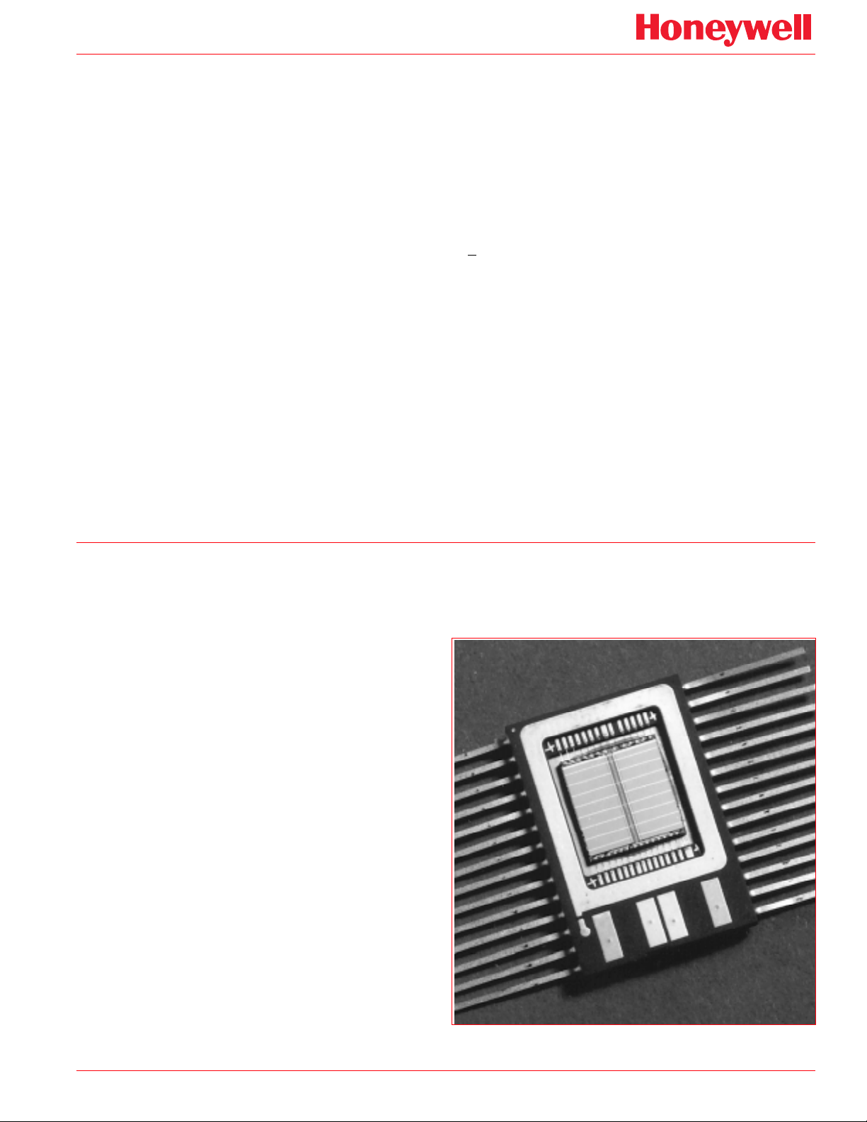
32K x 8 ROM—SOI HX6656
FEATURES
RADIATION
• Fabricated with RICMOS™ IV Silicon on Insulator
(SOI) 0.75 µm Process (L
= 0.6 µm)
eff
• Total Dose Hardness through 1x10⁶rad(SiO2)
• Dynamic and Static Transient Upset
Hardness through 1x10⁹ rad(Si)/s
• Dose Rate Survivability through 1x10¹¹ rad(Si)/s
14
-2
• Neutron Hardness through 1x10
cm
• SEU Immune
• Latchup Free
OTHER
• Read Cycle Times
< 17 ns (Typical)
≤ 25 ns (-55 to 125°C)
• Typical Operating Power <15 mW/MHz
• Asynchronous Operation
• CMOS or TTL Compatible I/O
• Single 5 V ± 10% Power Supply
• Packaging Options
- 28-Lead Flat Pack (0.500 in. x 0.720 in.)
- 28-Lead DIP, MIL-STD-1835, CDIP2-T28
- 36-Lead Flat Pack (0.630 in. x 0.650 in.)
GENERAL DESCRIPTION
The 32K x 8 Radiation Hardened ROM is a high performance 32,768 word x 8-bit read only memory with industrystandard functionality. It is fabricated with Honeywell’s
radiation hardened technology, and is designed for use in
systems operating in radiation environments. The ROM
operates over the full military temperature range and requires only a single 5 V ± 10% power supply. The ROM is
available with either TTL or CMOS compatible I/O. Power
consumption is typically less than 15 mW/MHz in operation,
and less than 5 mW when de-selected. The ROM operation
is fully asynchronous, with an associated typical access
time of 14 ns.
Honeywell’s enhanced SOI RICMOS™IV (Radiation Insensitive CMOS) technology is radiation hardened through the
use of advanced and proprietary design, layout, and process hardening techniques. The RICMOS™ IV process is a
5-volt, SIMOX CMOS technology with a 150 Å gate oxide
and a minimum drawn feature size of 0.75 µm (0.6 µm
effective gate length—L
tungsten via plugs, Honeywell’s proprietary SHARP planarization process, and a lightly doped drain (LDD) structure for improved short channel reliability.
). Additional features include
eff
Page 2
HX6656
FUNCTIONAL DIAGRAM
A:0-8,12-13
CE
NCS
NOE
A:9-11,14
11
Ro w
Decoder
•
•
•
CS • CE • OE
(0 = high Z)
32, 768 x 8
Memory
Array
• • •
Column Decoder
Data Output
Signal
8
1 = enab l ed
#
Q:0-7
Signal
All controls must b e
enabled for a signal to
pass. (#: numbe r of
4
buffers, default = 1)
SIGNAL DEFINITIONS
A: 0-14 Address input pins which select a particular eight-bit word within the memory array.
Q: 0-7 Data Output Pins.
NCS Negative chip select, when at a low level allows normal read operation. When at a high level NCS forces the
ROM to a precharge condition, holds the data output drivers in a high impedance state and disables all input
buffers except CE. If this signal is not used it must be connected to VSS.
NOE Negative output enable, when at a high level holds the data output drivers in a high impedance state. When
at a low level, the data output driver state is defined by NCS and CE. If this signal is not used it must be
connected to VSS.
CE* Chip enable, when at a high level allows normal operation. When at a low level CE forces the ROM to a
precharge condition, holds the data output drivers in a high impedance state and disables all the input buffers
except the NCS input buffer. If this signal is not used it must be connected to VDD.
TRUTH TABLE
NCS CE* NOE MODE Q
L H L Read Data Out
H X XX Deselected High Z
X L XX Disabled High Z
Notes:
X: VI=VIH or VIL
XX: VSS≤VI≤VDD
NOE=H: High Z output state maintained
for NCS=X, CE=X
*Not Available in 28-lead DIP or 28-Lead Flat Pack
2
Page 3
RADIATION CHARACTERISTICS
Total Ionizing Radiation Dose
HX6656
The ROM will meet all stated functional and electrical
specifications over the entire operating temperature range
after the specified total ionizing radiation dose. All electrical
and timing performance parameters will remain within
specifications after rebound at VDD = 5.5 V and T =125°C
extrapolated to ten years of operation. Total dose hardness
is assured by wafer level testing of process monitor transistors and ROM product using 10 keV X-ray and Co60
radiation sources. Transistor gate threshold shift correlations have been made between 10 keV X-rays applied at a
dose rate of 1x10⁵ rad(SiO2)/min at T = 25°C and gamma
rays (Cobalt 60 source) to ensure that wafer level X-ray
testing is consistent with standard military radiation test
environments.
Transient Pulse Ionizing Radiation
The ROM is capable of reading and retaining stored data
during and after exposure to a transient ionizing radiation
pulse of ≤1 µs duration up to 1x10⁹ rad(Si)/s, when applied
under recommended operating conditions. To ensure validity of all specified performance parameters before, during, and after radiation (timing degradation during transient pulse radiation (timing degradation during transient
pulse radiation is ≤10%), it is suggested that stiffening
capacitance be placed on or near the package VDD and
VSS, with a maximum inductance between the package
(chip) and stiffening capacitance of 0.7 nH per part. If
there are no operate-through requirements, typical circuit
board mounted de-coupling capacitors are recommended.
The ROM will meet any functional or electrical specification after exposure to a radiation pulse of ≤50 ns duration
up to 1x10¹¹ rad(Si)/s, when applied under recommended
operating conditions.
Neutron Radiation
The ROM will meet any functional or timing specification
after a total neutron fluence of up to 1x1014 cm-2 applied
under recommended operating or storage conditions. This
assumes an equivalent neutron energy of 1 MeV.
Single Event Phenomena
All storage elements within the ROM are immune to single
event upsets. No access time or other performance degradation will occur for LET 190 MeV/cm/mg
2
.
Latchup
The ROM will not latch up due to any of the above radiation
exposure conditions when applied under recommended
operating conditions. Fabrication with the SIMOX substrate material provides oxide isolation between adjacent
PMOS and NMOS transistors and eliminates any potential
SCR latchup structures. Sufficient transistor body tie connections to the p- and n-channel substrates are made to
ensure no source/drain snapback occurs.
RADIATION HARDNESS RATINGS (1)
Parameter
Total Dose ≥1x10
Transient Dose Rate Upset (3) ≥1x10
Transient Dose Rate Survivability (3) ≥1x10
Neutron Fluence ≥1x10
(1) Device will not latch up due to any of the specified radiation exposure conditions.
(2) Operating conditions (unless otherwise specified): VDD=4.5 V to 5.5 V, TA=-55°C to 125°C.
(3) Not guaranteed with 28–Lead DIP.
Limits (2)
6
9
11
14
3
Units
rad(SiO2)
rad(Si)/s
rad(Si)/s
2
N/cm
Test Conditions
TA=25°C
Pulse width ≤1 µs
Pulse width ≤50 ns, X-ray,
VDD=6.0 V, TA=25°C
1 MeV equivalent energy,
Unbiased, TA=25°C
Page 4
HX6656
ABSOLUTE MAXIMUM RATINGS (1)
Rating
Symbol
VDD Positive Supply Voltage (2) -0.5 7.0 V
VPIN Voltage on Any Pin (2) -0.5 VDD+0.5 V
TSTORE Storage Temperature (Zero Bias) -65 150 °C
TSOLDER Soldering Temperature • Time 270•5 °C•s
PD Total Package Power Dissipation (3) 2.5 W
IOUT DC or Average Output Current 25 mA
VPROT ESD Input Protection Voltage (4) 2000 V
ΘJC
TJ Junction Temperature 175 °C
(1)Stresses in excess of those listed above may result in permanent damage. These are stress ratings only, and operation at these levels is not
implied. Frequent or extended exposure to absolute maximum conditions may affect device reliability.
(2)Voltage referenced to VSS.
(3)ROM power dissipation (IDDSB + IDDOP) plus ROM output driver power dissipation due to external loading must not exceed this specification.
(4)Class 2 electrostatic discharge (ESD) input protection. Tested per MIL-STD-883, Method 3015 by DESC certified lab.
Thermal Resistance (Jct-to-Case)
Parameter
Min
28 FP/36 FP 2
28 DIP 10
Max
Units
°C/W
RECOMMENDED OPERATING CONDITIONS
Symbol
VDD Supply Voltage (referenced to VSS) 4.5 5.0 5.5 V
TA Ambient Temperature -55 25 125 °C
VPIN Voltage on Any Pin (referenced to VSS) -0.3 VDD+0.3 V
Parameter
Min
Description
MaxTyp
CAPACITANCE (1)
Symbol
CI Input Capacitance 7 pF
CO Output Capacitance 9 pF VIO=VDD or VSS, f=1 MHz
Parameter
Typical
(1)
Worst Case
Min
Max
Units
Test Conditions
VI=VDD or VSS, f=1 MHz
Units
(1) This parameter is tested during initial design characterization only.
4
Page 5

DC ELECTRICAL CHARACTERISTICS
HX6656
Symbol Parameter
Typical
(1)
Worst Case
Min
Max
(2)
Units
IDDSB1 Static Supply Current 1.5 mA
IDDSBMF Standby Supply Current - Deselected 1.5 mA
IDDOPR Dynamic Supply Current, Selected 4.0 mA
II Input Leakage Current -1 +1 µA
IOZ Output Leakage Current -1 +1 µA
VIL Low-Level Input Voltage
CMOS 0.3xVDD V
TTL 0.8 V VDD = 4.5V
VIH High-Level Input Voltage
CMOS 0.7xVDD V
TTL 2.2 V VDD = 5.5V
VOL Low-Level Output Voltage
0.4 V VDD = 4.5V, IOL = 10 mA
0.05 V VDD = 4.5V, IOL = 200 µA
VOH High-Level Output Voltage
(1) Typical operating conditions: VDD= 5.0 V,TA=25°C, pre-radiation.
(2) Worst case operating conditions: VDD=4.5 V to 5.5 V, -55°C to +125°C, post total dose at 25°C.
(3) All inputs switching. DC average current.
4.2 V VDD = 4.5V, IOH = -5 mA
VDD-0.05 V VDD = 4.5V, IOH = -200 µA
Test Conditions
VIH=VDD IO=0
VIL=VSS Inputs Stable
NCS=VDD, IO=0,
f=40 MHz
f=1 MHz, IO=0, CE=VIH=VDD
NCS=VIL=VSS
VSS≤VI≤VDD
VSS≤VIO≤VDD
Output=high Z
2.9 V Valid high
249Ω
DUT
output
CL>
50 pF*
*CL = 5 pF for TWLQZ, TSHQZ, TELQZ, and TGHQZ
Tester Equivalent Load Circuit
Vref1
Vref2
+
-
+
-
output
Valid low
output
5
Page 6

HX6656
READ CYCLE AC TIMING CHARACTERISTICS (1)
Worst Case (3)
Symbol Parameter Typical -55 to 125°C Units
(2) Min Max
TAVAVR Address Read Cycle Time 25 ns
TAVQV Address Access Time 25 ns
TAXQX Address Change to Output Invalid Time 3 ns
TSLQV Chip Select Access Time 25 ns
TSLQX Chip Select Output Enable Time 5 ns
TSHQZ Chip Select Output Disable Time 10 ns
TEHQV Chip Enable Access Time (4) 25 ns
TEHQX Chip Enable Output Enable Time (4) 5 ns
TELQZ Chip Enable Output Disable Time (4) 10 ns
TGLQV Output Enable Access Time 9 ns
TGLQX Output Enable Output Enable Time 0 ns
TGHQZ Output Enable Output Disable Time 9 ns
(1) Test conditions: input switching levels VIL/VIH=0.5V/VDD-0.5V (CMOS), VIL/VIH=0V/3V (TTL), input rise and fall times <1 ns/V, input and
output timing reference levels shown in the Tester AC Timing Characteristics table, capacitive output loading C
capacitive output loading CL=5 pF for TSHQZ, TELQZ TGHQZ. For CL >50 pF, derate access times by 0.02 ns/pF (typical).
(2) Typical operating conditions: VDD=5.0 V, TA=25°C, pre-radiation.
(3) Worst case operating conditions: VDD=4.5 V to 5.5 V, -55°C to +125°C, post total dose at 25°C.
(4) Chip Enable (CE) pin not available on 28-lead FP or DIP.
T
AVAVR
>50 pF, or equivalent
L
ADDRESS
T
AVQV
T
SLQV
T
AXQX
NCS
T
DATA OUT
HIGH
IMPEDANCE
SLQX
DATA VALID
T
SHQZ
CE
NOE
T
T
EHQX
EHQV
T
GLQX
T
GLQV
T
ELQZ
T
GHQZ
6
Page 7

DYNAMIC ELECTRICAL CHARACTERISTICS
Read Cycle
The ROM is asynchronous in operation, allowing the read
cycle to be controlled by address, chip select (NCS), or chip
enable (CE) (refer to Read Cycle timing diagram). To
perform a valid read operation, both chip select and output
enable (NOE) must be low and chip enable must be high.
The output drivers can be controlled independently by the
NOE signal. Consecutive read cycles can be executed with
NCS held continuously low, and with CE held continuously
high, and toggling the addresses.
For an address activated read cycle, NCS and CE must be
valid prior to or coincident with the activating address edge
transition(s). Any amount of toggling or skew between
address edge transitions is permissible; however, data
outputs will become valid TAVQV time following the latest
occurring address edge transition. The minimum address
activated read cycle time is TAVAV. When the ROM is
operated at the minimum address activated read cycle
time, the data outputs will remain valid on the I/O until
TAXQX time following the next sequential address transition.
HX6656
To control a read cycle with NCS, all addresses and CE
must be valid prior to or coincident with the enabling NCS
edge transition. Address or CE edge transitions can occur
later than the specified setup times to NCS, however, the
valid data access time will be delayed. Any address edge
transition, which occurs during the time when NCS is low,
will initiate a new read access, and data outputs will not
become valid until TAVQV time following the address edge
transition. Data outputs will enter a high impedance state
TSHQZ time following a disabling NCS edge transition.
To control a read cycle with CE, all addresses and NCS
must be valid prior to or coincident with the enabling CE
edge transition. Address or NCS edge transitions can
occur later than the specified setup times to CE; however,
the valid data access time will be delayed. Any address
edge transition which occurs during the time when CE is
high will initiate a new read access, and data outputs will
not become valid until TAVQV time following the address
edge transition. Data outputs will enter a high impedance
state TELQZ time following a disabling CE edge transition.
7
Page 8

HX6656
TESTER AC TIMING CHARACTERISTICS
TTL I/O Configuration
3 V
Input
Levels*
0 V
Output
Sense
Levels
High Z
High Z = 2.9V
3.4 V
2.4 V
* Input rise and fall times <1 ns/V
QUALITY AND RADIATION HARDNESS
ASSURANCE
VDD-0.4V
0.4 V
1.5 V
1.5 V
High Z
CMOS I/O Configuration
VDD-0.5 V
0.5 V
VDD/2
High Z
High Z = 2.9V
VDD-0.4V
3.4 V
2.4 V
0.4 V
High Z
VDD/2
Honeywell maintains a high level of product integrity through
process control, utilizing statistical process control, a complete “Total Quality Assurance System,” a computer data
base process performance tracking system, and a radiation-hardness assurance strategy.
The radiation hardness assurance strategy starts with a
technology that is resistant to the effects of radiation.
Radiation hardness is assured on every wafer by irradiating
test structures as well as product die, and then monitoring
key parameters which are sensitive to ionizing radiation.
Conventional MIL-STD-883C TM 5005 Group E testing,
which includes total dose exposure with Cobalt 60, may
also be performed as required. This Total Quality approach
ensures our customers of a reliable product by engineering
in reliability, starting with process development and continuing through product qualification and screening.
SCREENING LEVELS
Honeywell offers several levels of device screening to meet
your system needs. “Engineering Devices” are available
with limited performance and screening for breadboarding
and/or evaluation testing. Hi-Rel Level B and S devices
undergo additional screening per the requirements of MILSTD-883. As a QML supplier, Honeywell also offers QML
Class Q and V devices per MIL-PRF-38535 and are available per the applicable Standard Military Drawing (SMD).
QML devices offer ease of procurement by eliminating the
need to create detailed specifications and offer benefits of
improved quality and cost savings through standardization.
RELIABILITY
Honeywell understands the stringent reliability require
ments for space and defense systems and has extensive
experience in reliability testing on programs of this nature.
This experience is derived from comprehensive testing of
VLSI processes. Reliability attributes of the RICMOS
process were characterized by testing specially designed
irradiated and non-irradiated test structures from which
specific failure mechanisms were evaluated. These specific
mechanisms included, but were not limited to, hot carriers,
electromigration and time dependent dielectric breakdown.
This data was then used to make changes to the design
models and process to ensure more reliable products.
In addition, the reliability of the RICMOS
TM
process and
product in a military environment was monitored by testing
irradiated and non-irradiated circuits in accelerated dynamic life test conditions. Packages are qualified for product use after undergoing Groups B & D testing as outlined
in MIL-STD-883, TM 5005, Class S. The product is qualified
by following a screening and testing flow to meet the
customer’s requirements. Quality conformance testing is
performed as an option on all production lots to ensure the
ongoing reliability of the product.
TM
-
8
Page 9

PACKAGING
VSS
VDD
NWE
CE
A13
A8
A9
A11
NOE
A10
NCS
DQ7
DQ6
DQ5
DQ4
DQ3
VDD
VSS
VSS
VDD
A14
A12
A7
A6
A5
A4
A3
A2
A1
A0
DQ0
DQ1
DQ2
NC
VDD
VSS
36
35
34
33
32
31
30
29
28
27
26
25
24
23
22
21
20
19
Top
View
1
2
3
4
5
6
7
8
9
10
11
12
13
14
15
16
17
18
HX6656
The 32K x 8 ROM is offered in a custom 36-lead flat pack
(FP), 28-Lead FP, or standard 28-lead DIP. Each package
is constructed of multilayer ceramic (Al2O3) and features
internal power and ground planes. The 36-lead FP also
features a non-conductive ceramic tie bar on the lead
frame. The tie bar allows electrical testing of the device,
while preserving the lead integrity during shipping and
handling, up to the point of lead forming and insertion.
28-LEAD FP PINOUT
A14
A12
A7
A6
A5
A4
A3
A2
A1
A0
DQ0
DQ1
DQ2
VSS
1
2
3
4
5
6
7
8
9
10
11
12
13
14
Top
View
28
27
26
25
24
23
22
21
20
19
18
17
16
15
VDD
NWE
A13
A8
A9
A11
NOE
A10
NCS
DQ7
DQ6
DQ5
DQ4
DQ3
Ceramic chip capacitors can be mounted to the package to
maximize supply noise decoupling and increase board
packing density. These capacitors attach directly to the
internal package power and ground planes. This design
minimizes resistance and inductance of the bond wire and
package. All NC (no connect) pins should be connected
to VSS to prevent charge build up in the radiation
environment.
36-LEAD FP PINOUT
36-LEAD FLAT PACK
E
22018131-001
1
b
Top
D
HGL L
Ceramic
Body
J
I
A
C M
X
VDD
F
1
1
VSS
P
View
Optional
Capacitors
O
T
R
Y
VDD
Kovar
Lid [3]
N
VSS
V
W
U
9
(width)
(pitch)
Non-
Conductive
Tie-Bar
S
e
0.004
All dimensions are in inches
A
0.095 ± 0.014
b
0.008 ± 0.002
C
0.005 to 0.0075
D
0.650 ± 0.010
E
0.630 ± 0.007
e
0.025 ± 0.002 [2]
F
0.425 ± 0.005 [2]
G
0.525 ± 0.005
H
0.135 ± 0.005
I
0.030 ± 0.005
J
0.080 typ.
L
0.285 ± 0.015
[1] Parts delivered with leads unformed
[2] At tie bar
[3] Lid tied to VSS
M
N
O
P
R
S
T
U
V
W
X
Y
[1]
0.008 ± 0.003
0.050 ± 0.010
0.090 ref
0.015 ref
0.075 ref
0.113 ± 0.010
0.050 ref
0.030 ref
0.080 ref
0.005 ref
0.450 ref
0.400 ref
Page 10

HX6656
28-LEAD FLAT PACK (22017842-001)
E
1
TOP
F
L
W
A
G
Q
VIEW
X
Y
Kovar
Lid [4]
E2
28-LEAD DIP (22017785-001)
Capacitor
Pads
Ceramic
Body
E3
C
b
(width)
e
(pitch)
U
Lead
Alloy 42 [3]
Index
D
BOTTOM
VIEW
S
All dimensions in inches
1
[1] BSC – Basic lead spacing between centers
[2] Where lead is brazed to package
[3] Parts delivered with leads unformed
[4] Lid connected to VSS
A
0.105 ± 0.015
b
0.017 ± 0.002
C
0.003 to 0.006
D
0.720 ± 0.008
e
0.050 ± 0.005 [1]
E
0.500 ± 0.007
E2
0.380 ± 0.008
E3
0.060 ref
F
0.650 ± 0.005 [2]
G
0.035 ± 0.004
L
0.295 min [3]
Q
0.026 to 0.045
S
0.045 ± 0.010
U
0.130 ref
W
0.050 ref
X
0.075 ref
Y
0.010 ref
For 28-Lead DIP description, see MIL-STD-1835, Type CDIP2-T28, Config. C, Dimensions D-10
10
Page 11

HX6656
DYNAMIC BURN-IN DIAGRAM*
VDD
1
A14
VSS
R
2
A12
R
3
A7
R
4
A6
R
5
A5
R
6
A4
R
7
A3
R
8
A2
R
9
A1
R
10
A0
R
11
DQ0
R
12
DQ1
R
13
DQ2
R
14
VSS
32K x 8 ROM
F16
F7
F6
F5
F4
F3
F2
F8
F13
F14
F1
F1
F1
VDD = 6.5V, R ≤ 10 KΩ, VIH = VDD, VIL = VSS
Ambient Temperature ≥ 125 °C, F0 ≥ 100 KHz Sq Wave
Frequency of F1 = F0/2, F2 = F0/4, F3 = F0/8, etc.
VDD
NC
A13
A8
A9
A11
NOE
A10
NCS
DQ7
DQ6
DQ5
DQ4
DQ3
28
27
R
26
25
24
23
22
21
20
19
18
17
16
15
F0
F15
R
R
F12
F11
R
R
F10
F17
R
R
F9
R
F17
R
F1
R
F1
R
F1
R
F1
R
F1
STATIC BURN-IN DIAGRAM*
VDD
1
R
R
R
R
R
R
R
R
R
R
R
R
R
VSS
A14
2
A12
3
A7
4
A6
5
A5
6
A4
7
A3
8
A2
9
A1
10
A0
11
DQ0
12
DQ1
13
DQ2
14
VSS
VDD = 5.5V, R ≤ 10 KΩ
Ambient Temperature ≥ 125 °C
28
VDD
27
NC
26
A13
25
A8
24
A9
23
A11
22
NOE
21
A10
20
NCS
19
DQ7
32K x 8 ROM
DQ6
DQ5
DQ4
DQ3
18
17
16
15
VDD
R
R
R
R
R
R
R
R
R
R
R
R
R
R
*36-lead Flat Pack burn-in diagrams have similar connections and are available on request.
ROM CODE
The ROM code can be provided to Honeywell via FTP, E-Mail or a variety of magnetic storage media, including
3.5 inch floppy disc, 4m digital tape and others.
The ROM Code data file should contain the following format:
<address> [/] <data> [;] [Comment]
Where items enclosed in ‘[‘and’]’ are optional.
The address and data must be hex numbers in the form, MSB...LSB. The “/” and the “;” are optional and any
characters after the “#” are comments. For example the following input file, all of the lines are valid:
000 d4
001 / 32
002 1d
003 / 72;
4/5e; # all of these lines are in valid format
11
Page 12

HX6656
ORDERING INFORMATION (1)
H
SOURCE
H=HONEYWELL
(1) Orders may be faxed to 612-954-2051. Please contact our Customer Logistics Department at 612-954-2888 for further information.
(2) Engineering Device description: Parameters are tested from -55 to 125°C, 24 hr burn-in, no radiation guaranteed.
Contact Factory with other needs.
X
PROCESS
X=SOI
6656
PART NUMBER
PACKAGE DESIGNATION
N=28-Lead FP
R=28-Lead DIP
X=36-Lead FP
K=Known Good Die
- = Bare die (No Package)
N
S
SCREEN LEVEL
V=QML Class V
Q=QML Class Q
S=Level S
B=Level B
E=Engr Device (2)
R=1x10⁵ rad(SiO2)
F=3x10⁵ rad(SiO2)
H=1x10⁶ rad(SiO2)
N=No Level Guaranteed
H
TOTAL DOSE
HARDNESS
C
INPUT
BUFFER TYPE
C=CMOS Level
T=TTL Level
To learn more about Honeywell Solid State Electronics Center,
visit our web site at http://www.ssec.honeywell.com
Honeywell reserves the right to make changes to any products or technology herein to improve reliability, function or design. Honeywell does not assume any liability
arising out of the application or use of any product or circuit described herein; neither does it convey any license under its patent rights nor the rights of others.
Helping You Control Your World
900154
2/96
 Loading...