

Page 1
HX6408
Advanced Information
HX6408
512k x 8 STATIC RAM
The 512K x 8 Radiation Hardened Static RAM is a high
performance 524,288 word x 8-bit static random access
memory with optional industry-standard functionality. It is
fabricated with Honeywell’s radiation hardened Silicon On
Insulator (SOI) technology, and is designed for use in low
voltage systems operating in radiation environments. The
RAM operates over the full military temperature range and
requires only a single 3.3 V ± 0.3V power supply. Power
consumption is typically <30 mW @ 1MHz in write mode,
<14 mW @ 1MHz in read mode, and is less than 5 mW
when in standby mode.
Honeywell’s enhanced RICMOS™(Radiation Insensitive
CMOS) SOI V technology is radiation hardened through the
use of advanced and proprietary design, layout and process
hardening techniques.
FEATURES
Fabricated with RICMOS™ V
Silicon On Insulator (SOI)
0.35 mm Process (Leff = 0.28 µm)
Total Dose ≥ 3x10⁵ and 1X10⁶ rad(SiO2)
Neutron ≥1x1014 cm-2
Dynamic and Static Transient Upset
≥1x10
Dose Rate Survivability ≥1x10¹² rad(Si)/s
Soft Error Rate
≤1x10
10
rad(Si)/s (3.3 V)
-10
Upsets/bit-day (3.3 V)
No Latchup
Read/Write Cycle Times
≤20 ns, (3.3 V), -55 to 125°C
Typical Operating Power (3.3 V)
<14 mW @ 1MHz Read
<30 mW @ 1MHz Write
<5 mW Standby mode
Asynchronous Operation
CMOS Compatible I/O
The RICMOS™ V low power process is a SOI CMOS
technology with an 80 Å gate oxide and a minimum
drawn feature size of 0.35 µm. Additional features
include tungsten via and contact plugs, Honeywell’s
proprietary SHARP planarization process and a lightly
doped drain (LDD) structure for improved short
channel reliability. A seven transistor (7T) memory cell
is used for superior single event upset hardening,
while three layer metal power busing and the low
collection volume SOI substrate provide improved
dose rate hardening.
Single Power Supply,
3.3 V ± 0.3 V
Operating Range is
-55°C to +125°C
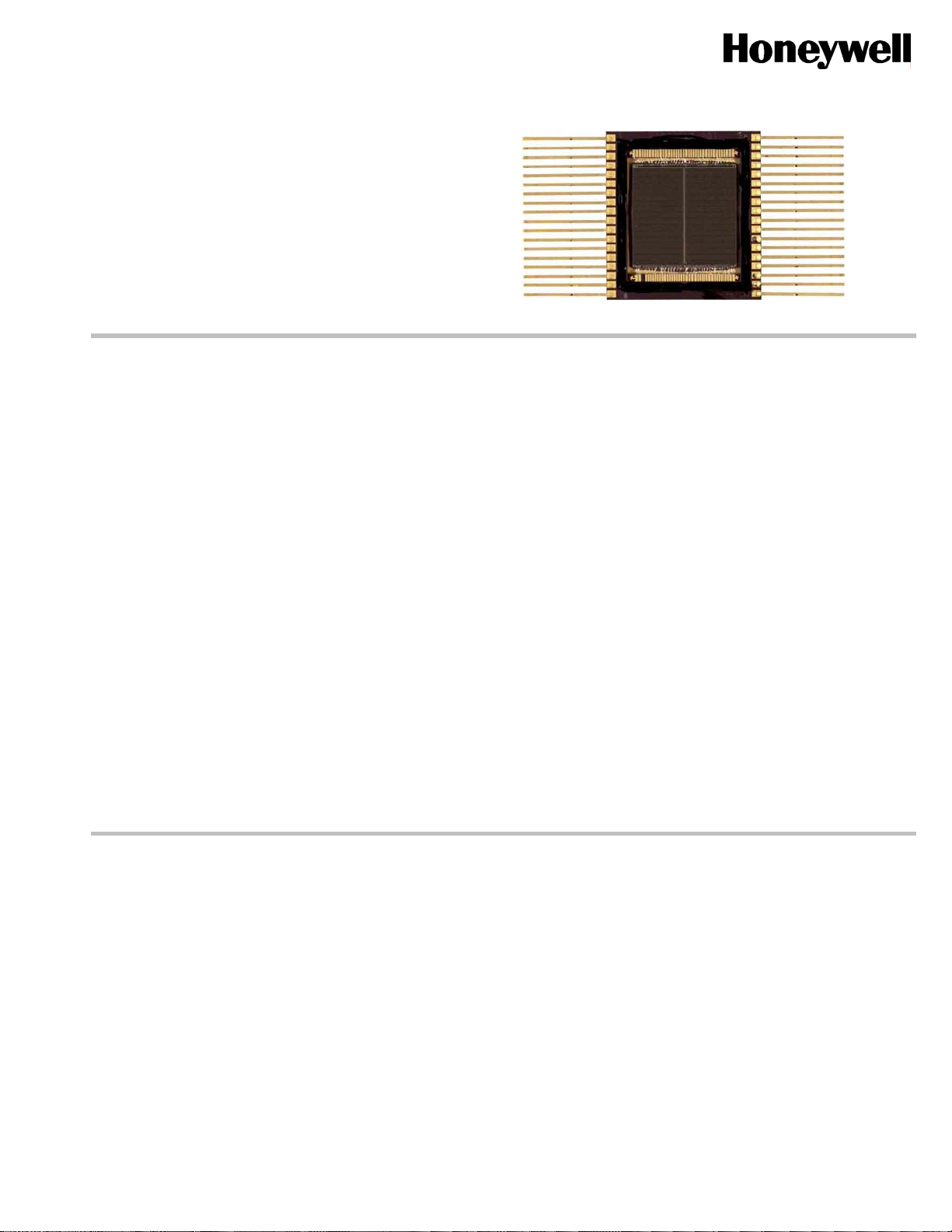
36-Lead Flat Pack Package
Optional Low Power Sleep
Mode
1 www.honeywell.com
Page 2
HX6408
y
Advanced Information
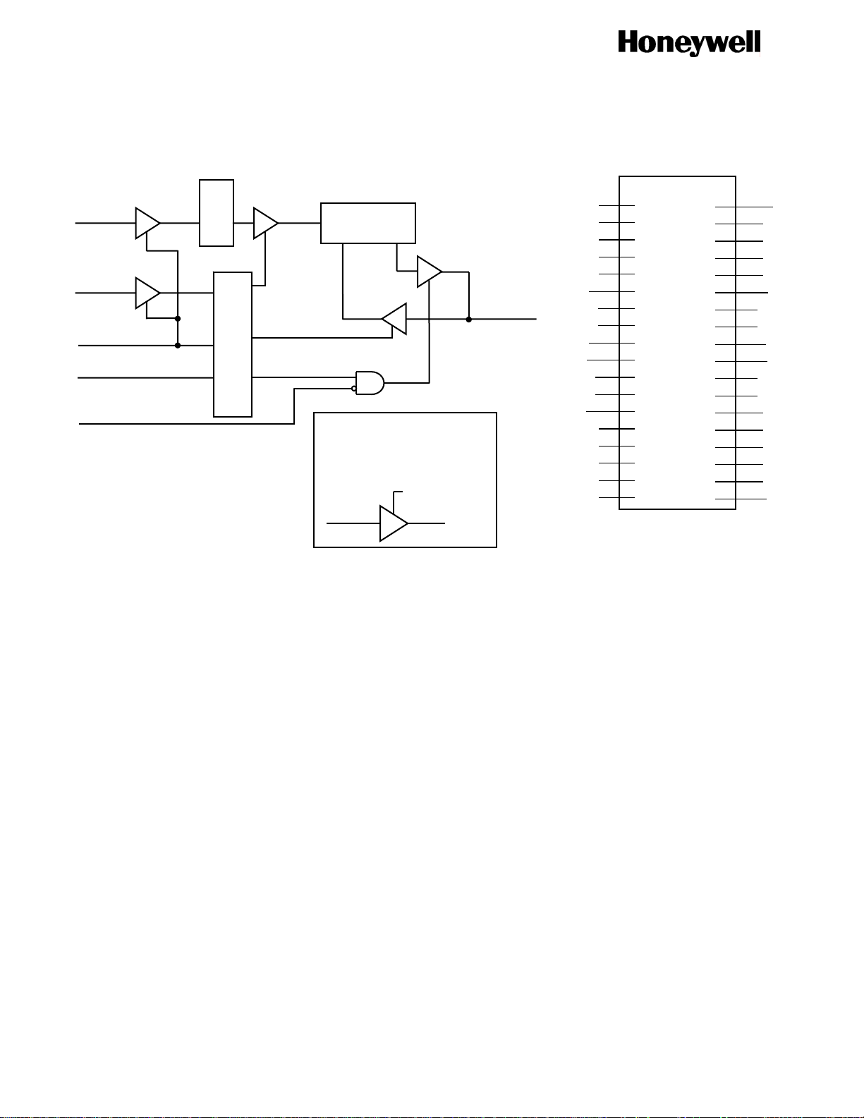
FUNCTIONAL DIAGRAM 36 LEAD FLAT PACK PINOUT
Address
Decoder
Memory
Arra
NWE
NSL
NCS
NOE
WE • CS
NWE • CS
Timing \ Control
All controls must be enabled
for signal to pass.
# = number of buffers,
Default = 1
1 = enabled
Signal
Signal
#
DQ(0:7)
NCS 6
VDD 9
VSS 10
NWE 13
SIGNAL DEFINITIONS
A: 0-18 Address input pins, which select a particular eight-bit word within the memory array.
DQ: 0-7 Bidirectional data pins, which serve as data outputs during a read operation and as data inputs
during a write operation.
NCS Negative chip select, when at a low level allows normal read or write operation. When at a high level
NCS forces the SRAM to a precharge condition, holds the data output drivers in a high impedance
state. If this signal is not used it must be connected to VSS.
NWE Negative write enable, when at a low level activates a write operation and holds the data output
drivers in a high impedance state. When at a high level NWE allows normal read operation.
NOE Negative output enable, when at a high level holds the data output drivers in a high impedance
state. When at a low level, the data output driver state is defined by NCS, NWE and NSL. This
signal is asynchronous.
NSL Not sleep, when at a high level allows normal operation. When at a low level NSL forces the SRAM
to a precharge condition, holds the data output drivers in a high impedance state and disables all the
input buffers except the NCS and NOE input buffers. If this signal is not used it must be connected
to VDD. This signal is asynchronous. The HX6408 may be ordered without the sleep mode option
and pin 36 is then a NC.
A0 1
A1 2
A2 3
A3 4
A4 5
D0 7
D1 8
D2 11
D3 12
A5 14
A6 15
A7 16
A8 17
A9 18
HX6408
Top View
36 (NSL)
35 A18
34 A17
33 A16
32 A15
31 NOE
30 D4
29 D5
28 VSS
27 VDD
26 D6
25 D7
24 A14
23 A13
22 A12
21 A11
20 A10
19 NAS
2 www.honeywell.com
Page 3
HX6408
Advanced Information
TRUTH TABLE
NCS NSL NWE NOE Mode DQ
L H H L Read Data Out
L H L X Write Data In
H X X X Deselected High Z
X L X X Sleep High Z
X: VI = VIH or VIL,
NOE=H: High Z output state maintained for NCS=X, NWE=X
RADIATION
Total Ionizing Radiation Dose
The SRAM will meet all stated functional and electrical
specifications over the entire operating temperature
range after the specified total ionizing radiation dose.
All electrical and timing performance parameters will
remain within specifications. Total dose hardness is
assured by wafer level testing of process monitor
transistors and RAM product using 10 KeV X-ray.
Transistor gate threshold shift correlations have been
made between 10 KeV X-rays applied at a dose rate of
5
1x10
rad(SiO
(Cobalt 60 source) to ensure that wafer level X-ray
testing is consistent with standard military radiation test
environments.
Transient Pulse Ionizing Radiation
The SRAM is capable of writing, reading, and retaining
stored data during and after exposure to a transient
ionizing radiation pulse, up to the specified transient
dose rate upset specification, when applied under
recommended operating conditions. It is recommended
to provide external power supply decoupling capacitors
to maintain VDD voltage levels during transient events.
The SRAM will meet any functional or electrical
specification after exposure to a radiation pulse up to
the transient dose rate survivability specification, when
applied under recommended operating conditions.
Note that the current conducted during the pulse by the
RAM inputs, outputs, and power supply may
2
)/min at T= 25°C and gamma rays
significantly exceed the normal operating levels. The
application design must accommodate these effects.
Neutron Radiation
The SRAM will meet any functional or timing
specification after exposure to the specified neutron
fluence under recommended operating or storage
conditions. This assumes an equivalent neutron energy
of 1 MeV.
Soft Error Rate
The SRAM is capable of meeting the specified Soft
Error Rate (SER), under recommended operating
conditions.
This hardness level is defined by the Adams 90%
worst case cosmic ray environment for
geosynchronous orbits.
Latchup
The SRAM will not latch up due to any of the above
radiation exposure conditions when applied under
recommended operating conditions. Fabrication with
the SOI substrate material provides oxide isolation
between adjacent PMOS and NMOS transistors and
eliminates any potential SCR latchup structures.
Sufficient transistor body tie connections to the p- and
n-channel substrates are made to ensure no
source/drain snapback occurs.
3 www.honeywell.com
Page 4
HX6408
Advanced Information
RADIATION HARDNESS RATINGS (1)
Parameter Limits (2) Units Test Conditions
Total Dose
Transient Dose Rate Upset
Transient Dose Rate Survivability
Soft Error Rate
Neutron Fluence
(1) Device will not latch up due to any of the specified radiation exposure conditions.
(2) Operating conditions (unless otherwise specified): VDD=3.0V to 3.6V, TA=-55
ABSOLUTE MAXIMUM RATINGS (1)
VDD Supply Voltage Range (2) -0.5 4.6 V
VPIN Voltage on Any Pin (2) -0.5 VDD+0.5 V
TSTORE Storage Temperature (Zero Bias) -65 150 °C
TSOLDER Soldering Temperature (5 seconds) 270 °C
PD Maximum Power Dissipation (3) 2.5 W
IOUT DC or Average Output Current 25 mA
VPROT EST Input Protection Voltage (4) 2000 V
TJ Junction Temperature 175 °C
(1) Stresses in excess of those listed above may result in permanent damage. These are stress ratings only, and operation at these levels is
not implied. Frequent or extended exposure to absolute maximum conditions may affect device reliability.
(2) Voltage referenced to VSS.
(3) RAM power dissipation (IDDSB + IDDOP) plus RAM output driver power dissipation due to external loading must not exceed this
specification.
(4) Class 2 electrostatic discharge (ESD) input protection. Tested per MIL-STD-883, Method 3015 by DSEC certified lab.
RECOMMENDED OPERATING CONDITIONS
VDD Supply Voltage (referenced to VSS) 3.0 3.3 3.6 V
TA Ambient Temperature -55 25 125 °C
VPIN Voltage on Any Pin (referenced to VSS) -0.3 VDD+0.3 V
VDDRAMP VDD Turn on ramp time 50 ms
≥3X10⁵
6
≥1X10
rad(SiO
) TA=25°C
2
≥1X10¹⁰ rad(Si)/s Pulse width ≤50 ns
≥1X10
12
VDD>3.6V, T
rad(Si)/s Pulse width ≤50 ns, X-
=25°C
A
ray,VDD=3.6V,
T
=25°C
A
<1X10
-10
Upsets/bit-day TA= 85°C, Adams 90%
worst case environment
≥1X10¹⁴ N/cm2 1MeV equivalent
energy, Unbiased,
T
=25°C
A
o
C to 125oC
Rating Symbol Parameter
Units
Min Max
36 Pin FP 2 ΘJC Thermal Resistance (Jct-to-Case)
Description Symbol Parameter
°C/W
Units
Min Typ Max
4 www.honeywell.com
Page 5

HX6408
Advanced Information
DC ELECTRICAL CHARACTERISTICS
Worst Case (1) Symbol Parameter
Min Max
IDDSB Static Supply Current
TA=25°C
TA=125°C
IDDOP3 Static Supply Current
Deselected
IDDOPW Dynamic Supply Current,
Selected (Write)
1 MHz
2 MHz
10 MHz
25 MHz
40 MHz
IDDOPR Dynamic Supply Current,
Selected (Read)
1 MHz
2 MHz
10 MHz
25 MHz
40 MHz
IDDOP1 Dynamic Supply Current,
Deselected
IDDOP2 Dynamic Supply Current,
Sleep
II Input Leakage Current -5 5 µA Vss VI VDD
IOZ Output Leakage Current -10 10 µA Vss VIO
VIL Low-Level Input Voltage 0.3xVDD V VDD=3.0V
VIH High-Level Input Voltage 0.7xVDD V VDD=3.6V
VOL Low-Level Output Voltage 0.4 V VDD=3.0V, IOL = 8mA
VOH High-Level Output Voltage 2.7 V VDD=3.0V, IOH = 4mA
(1) Worst case operating conditions: VDD=3.0V to 3.6V, -55°C to +125°C, post total dose at 25°C.
(2) All inputs switching. DC average current.
5
10
24 mA VDD=max, Iout=0mA,
9
18
89
160
260
4
8
40
100
160
1.5 mA VDD=max, Iout=0mA,
0.2 mA VDD=max, Iout=0mA,
CAPACITANCE (1)
Worst Case (1) Symbol Parameter
Min Max
CI Input Capacitance 9 pF VI=VDD or VSS, f=1 MHz
CO Output Capacitance 8 pF VIO=VDD or VSS, f=1 MHz
(1) This parameter is tested during initial design characterization only.
Units Test Conditions
Units Test Conditions
mA
mA/MHz
mA/MHz
VDD=max, Iout=0mA,
Inputs Stable
f=fmax, NSL=NCS=VIH (2)
VDD=max, Iout=0mA,
NSL=VIH, NCS=VIL (1)
VDD=max, Iout=0mA,
NSL=VIH, NCS=VIL (1)
f=1MHz, NSL=VIH (2)
f=1MHz, NSL=VIL (2)
VDD output = high Z
5 www.honeywell.com
Page 6

HX6408
V
V
V
(
Advanced Information
DATA RETENTION CHARACTERISTICS
Worst Case (2) Symbol Parameter Typical
(1)
VDR Data Retention Voltage 2.0 V NCS=VDR
IDR Data Retention Current 3 mA NCS=VDD=VDR
(1) Typical operating conditions: TA=25°C, pre-radiation.
(2) Worst case operating conditions: TA=-55°C to +125°C, post dose at 25°C
Min Max
TESTER EQUIVALENT LOAD CIRCUIT
1.9V
V1
Units Test Conditions
VI=VDR or VSS
VI=VRD or VSS
Valid High
Output
DUT
249
Output
CL < 50 pf *
* C
= 5pf for TWQZ, TSHQZ, TPLQZ, and TGHQZ
L
Tester AC Timing Characteristics
Input Levels *
* Input rise and fall times <5 ns.
Output Sense
High Z = VDD/2
DD
SS
V2
Valid Low
Output
DD/2
VDD – 0.4V
High Z
0.4V
High Z
VDD/2) + 0.2V
(VDD/2) - 0.2V
6 www.honeywell.com
Page 7

HX6408
Advanced Information
ASYCHRONOUS READ CYCLE AC TIMING CHARACTERISTICS (1)
Symbol Parameter
Typical
(2)
TAVAVR Address Read Cycle Time 300KRad
1MRad
TAVQV Address Access Time 300KRad
1MRad
TAXQX Address Change to Output Invalid Time 3 ns
TSLQV Chip Select Access Time 300KRad
1MRad
TSLQX Chip Select Output Enable Time 4 ns
TSHQZ Chip Select Output Disable Time 8 ns
TPHQV Sleep Enable Access Time 25 ns
TPHQX Sleep Enable Output Enable Time 5 ns
TPLQZ Sleep Enable Output Disable Time 10 ns
TGLQV Output Enable Access Time 5 ns
TGLQX Output Enable Output Enable Time 0 ns
TGHQZ Output Enable Output Disable Time 5 ns
(1) Test conditions: input switching levels, VIL/VIH=0V/3V, input rise and fall times <1 ns/V, input and output timing reference levels shown in
the Tester AC Timing Characteristics table, capacitive output loading C
TSHQZ, TPLQZ TGHQZ. For C
(2) Typical operating conditions: VDD=3.3V, TA=25°C, pre-radiation.
(3) Worst case operating conditions: VDD=3.0V to 3.6V, TA=-55°C to 125°C, post total dose 25°C at
>50 pF, derate access times by 0.02 ns/pF (typical).
L
20
20
20
≥50 pF, or equivalent capacitive output loading CL=5 pF for
L
T
AVAVR
Worst Case (3)
-55 to 125°C
Min Max
ns
25
25
25
Units
ns
ns
ADDRESS
NCS
DATA OUT
NSL
NOE
7 www.honeywell.com
HIGH
IMPEDANCE
T
PHQV
T
T
T
PHQX
T
GLQX
AVQV
T
SLQX
T
SLQV
GLQV
T
DATA VALID
AXQX
T
SHQZ
T
PLQZ
T
GHQZ
Page 8

HX6408
Advanced Information
ASYNCHRONOUS WRITE CYCLE AC TIMING CHARACTERISTICS (1)
Symbol Parameter
Typical
(2)
TAVAVW Write Cycle Time (4) 300KRad
1MRad
TWLWH Write Enable Write Pulse Width 300KRad
1MRad
TSLWH Chip Select to End of Write Time 300KRad
1MRad
TDVWH Data Valid to End of Write Time 300KRad
1MRad
TAVWH Address Valid to End of Write Time 300KRad
1MRad
TWHDX Data Hold after End of Write Time 0 ns
TAVWL Address Valid Setup to Start of Write Time 0 ns
TWHAX Address Valid Hold after End of Write Time 0 ns
TWLQZ Write Enable to Output Disable Time 7 ns
TWHQX Write Disable to Output Enable Time 4 ns
TWHWL Write Disable to Write Enable Pulse Width (5) 5 ns
(1) Test conditions: input switching levels, VIL/VIH=0V/3V, input rise and fall times <1 ns/V, input and output timing reference levels shown in
the Tester AC Timing Characteristics table, capacitive output loading ≥50 pF, or equivalent capacitive load 5 pF for TWLQZ.
(2) Typical operating conditions: VDD=3.3V, TA=25°C, pre-radiation.
(3) Worst case operating conditions: VDD=3.0V to 3.6V, -55°C to 125°C, post total dose 25°C
(4) TAVAVW = TWLWH + TWHWL
(5) Guaranteed but not tested
20
15
16
12
20
T
AVAVW
Worst Case (3)
-55 to 125°C
Min Max
ns
25
ns
20
ns
20
ns
15
ns
25
Units
ADDRESS
T
T
NWE
DATA OUT
DATA IN
NCS
NSL
HIGH
IMPEDANCE
8 www.honeywell.com
AVWL
T
PHWH
T
WLQZ
T
T
T
SLWH
AVWH
T
DVWH
DATA VALID
T
WHAX
T
WHQX
T
Page 9

HX6408
Advanced Information
DYNAMIC ELECTRICAL CHARACTERISTICS
Asynchronous Operation
The RAM is asynchronous in operation. Read and
Write cycles are controlled by NWE, NCS, NSL, and
Address signals.
Read Operation
To perform a valid read operation, both chip select
and output enable (NOE) must be low and not sleep
(NSL) and write enable (NWE) must be high. The
output drivers can be controlled independently by the
NOE signal.
To perform consecutive read operations, NCS is
required to be held continuously low, NSL held
continuously high, and the toggling of the addresses
will start the new read cycle.
It is important to have the address bus free of noise
and glitches, which can cause inadvertent read
operations. The control and address signals should
have rising and falling edges that are fast (<5 ns) and
have good signal integrity (free of noise, ringing or
steps associated reflections).
For an address activated read cycle, NCS and NSL
must be valid prior to or coincident with the address
edge transition(s). Any amount of toggling or skew
between address edge transitions is permissible;
however, data outputs will become valid TAVQV time
following the latest occurring address edge transition.
The minimum address activated read cycle time is
TAVAV. When the RAM is operated at the minimum
address activated read cycle time, the data outputs
will remain valid on the RAM I/O until TAXQX time
following the next sequential address transition.
To control a read cycle with NCS, all addresses and
NSL must be valid prior to or coincident with the
enabling NCS edge transition. Address or NSL edge
transitions can occur later than the specified setup
times to NCS; however, the valid data access time will
be delayed. Any address edge transition, which
occurs during the time when NCS is low, will initiate a
new read access, and data outputs will not become
valid until TAVQV time following the address edge
transition. Data outputs will enter a high impedance
state TSHQZ time following a disabling NCS edge
transition.
To control a read cycle with NSL, all addresses and
NCS must be valid prior to or coincident with the
enabling NSL edge transition. Address or NCS edge
transitions can occur later than the specified setup
times to NSL; however, the valid data access time will
be delayed. Any address edge transition, which
occurs during the time when NSL is high will initiate a
new read access, and data outputs will not become
valid until TAVQV time following the address edge
transition. Data outputs will enter a high impedance
state TPLQZ time following a disabling NSL edge
transition.
Write Operation
To perform a write operation, both NWE and NCS
must be low, and NSL must be high.
Consecutive write cycles can be performed by
toggling one of the control signals while the other
remains in their “write” state (NWE or NCS held
continuously low, or NSL held continuously high). At
least one of the control signals must transition to the
opposite state between consecutive write operations.
The write mode can be controlled via three different
control signals: NWE, NCS, and NSL. All three modes
of control are similar, except the NCS and NSL
controlled modes actually disable the RAM during the
write recovery pulse. NSL fully disables the RAM
decode logic and input buffers for power savings.
Only the NWE controlled mode is shown in the table
and diagram on the previous page for simplicity;
however, each mode of control provides the same
write cycle timing characteristics. Thus, some of the
parameter names referenced below are not shown in
the write cycle table or diagram, but indicate which
control pin is in control as it switches high or low. To
write data into the RAM, NWE and NCS must be held
low and NSL must be held high for at least
WLWH/TSLSH/TPHPH time. Any amount of edge
skew between the signals can be tolerated, and any
one of the control signals can initiate or terminate the
write operation. The DATA IN must be valid TDVWH
time prior to switching high.
For consecutive write operations, write pulses (NWE)
must be separated by the minimum specified
WHWL/TSHSL/TPLPL time. Address inputs must be
valid at least TAVWL/TAVSL/TAVPH time before the
enabling NWE/NCS/NSL edge transition, and must
remain valid during the entire write time. A valid data
overlap of write pulse width time of TDVWH/TDVSH/
TDVPL, and an address valid to end of write time of
TAVWH/TAVSH/TAVPL also must be provided for
during the write operation. Hold times for address
inputs and data inputs with respect to the disabling
NWE/NCS/NSL edge transition must be a minimum of
TWHAX/TSHAX/TPLPX time and TWHDX/TSHDX
9 www.honeywell.com
Page 10

HX6408
Advanced Information
/TPLDX time, respectively. The minimum write cycle
time is TAVAV.
QUALITY AND RADIATION HARDNESS ASSURANCE
Honeywell maintains a high level of product integrity
through process control, utilizing statistical process
control, a complete
“Total Quality Assurance System,” a computer data
base process performance tracking system and a
radiation-hardness assurance strategy.
The radiation hardness assurance strategy starts with
a technology that is resistant to the effects of
radiation. Radiation hardness is assured on every
wafer by irradiating test structures as well as SRAM
product, and then monitoring key parameters, which
are sensitive to ionizing radiation. Conventional MILSTD-883 TM 5005 Group E testing, which includes
total dose exposure with Cobalt 60, may also be
performed as required. This Total Quality approach
ensures our customers of a reliable product. It starts
with process development and continuing through
product qualification and screening.
SCREENING LEVELS
Honeywell offers several levels of device screening to
meet your system needs. “Engineering Devices” are
available with limited performance and screening for
operational evaluation testing. Hi-Rel Level B and S
devices undergo additional screening per the
requirements of MILSTD-883. As a QML supplier,
Honeywell also offers QML Class Q and V devices
per MIL-PRF-38535 and are available per the
applicable Standard Microcircuit Drawing (SMD). QML
devices offer ease of procurement by eliminating the
need to create detailed specifications and offer
benefits of improved quality and cost savings through
standardization.
RELIABILITY
Honeywell understands the stringent reliability
requirements for space and defense systems and has
extensive experience in reliability testing on programs
of this nature. This experience is derived from
comprehensive testing of VLSI processes. Reliability
attributes of the RICMOS™ SOI process were
characterized by testing specially designed irradiated
and non-irradiated test structures from which specific
failure mechanisms were evaluated. These specific
mechanisms included, but were not limited to, hot
carriers, electromigration and time dependent
dielectric breakdown. This data was then used to
make changes to the design models and process to
ensure more reliable products.
In addition, the reliability of the RICMOS™ SOI
process and product in a military environment is
monitored by testing
irradiated and non-irradiated circuits in accelerated
dynamic life test conditions. Packages were qualified
for product use after undergoing Groups B & D testing
as outlined in MIL-STD-883, TM 5005, Class S.
Quality conformance testing is performed as an option
on all production lots to ensure the ongoing reliability
of the product.
PACKAGING
The 512K x 8 SRAM is offered in a commercially
compatible 36-lead flat pack. This package is
constructed of multi-layer ceramic (Al
contains internal power and ground planes.
Parentheses denote pin options. These pins are
2O3) and
10 www.honeywell.com
available as NC to conform to commercial
standards. All NC (no connect) pins should be
connected to VSS to prevent charge build up in
the radiation environment.
Page 11

HX6408
Advanced Information
PACKAGE OUTLINE
COMMON DIMENSIONS
SYM MIN. NOM. MAX.
A .102 .113 .125
A1 .085 .095 .105
B .016 .018 .020
C .004 .006 .008
D .910 .920 .930
E .045 .050 .055
E1 .832 .840 .848
L ----- .450 ----Q ----- .104 -----
ORDERING INFORMATION (1)
H X
6408
PROCESS
X = SOI
PART NUMBER
V = QML Class V Equivalent (4)
Q = QML Class Q Equivalent (4)
Source
H = Honeywell
PACKAGE DESIGNATION
X = 36 Lead FP
K = Known Good Die
- = Bare Die (no package)
(1) Orders may be faxed to 763-954-2051. Please contact our Customer Service Representative at 763-954-2888 for further information.
(2) Engineering Device Description: Parameters are tested -55
(3) With the Non-Sleep Mode option, Pin 36 is a no-connect (NC), and is not wirebonded to the chip. With the Sleep Mode, Pin 36 has the
NSL function.
(4) These devices are screened to QML levels but are not QML certified.
For more information about Honeywell’s family of radiation hardened integrated circuit products and services,
visit www.myspaceparts.com
.
Honeywell reserves the right to make changes to any products or technology herein to improve reliability, function or design. Honeywell does not assume any
liability arising out of the application or use of any product or circuit described herein; neither does it convey any license under its patent rights nor the rights of
others.
Honeywell International Inc.
Aerospace Electronics Systems
Defense & Space Electronics Systems
12001 Highway 55
Plymouth, MN 55441
11 www.honeywell.com
1-800-323-8295
Form #900918
June 2005
©2005 Honeywell International Inc.
S H X
SCREEN LEVEL
S = Level S
E = Eng. Model (2)
TOTAL DOSE HARDNESS
R = 1x10⁵ rad (SiO2)
F = 3x10
H = 1x10
N = No Level Guaranteed (2)
°C to 125°C, 24 hour burn-in, IDDSB = 10 mA, no radiation Guaranteed.
5
rad (SiO2)
6
rad (SiO2)
N
MODE (3)
N = Non-Sleep Mode
M = Sleep Mode
 Loading...