

Honeywell HX6356 User Manual
查询HX6356供应商
Aerospace Electronics
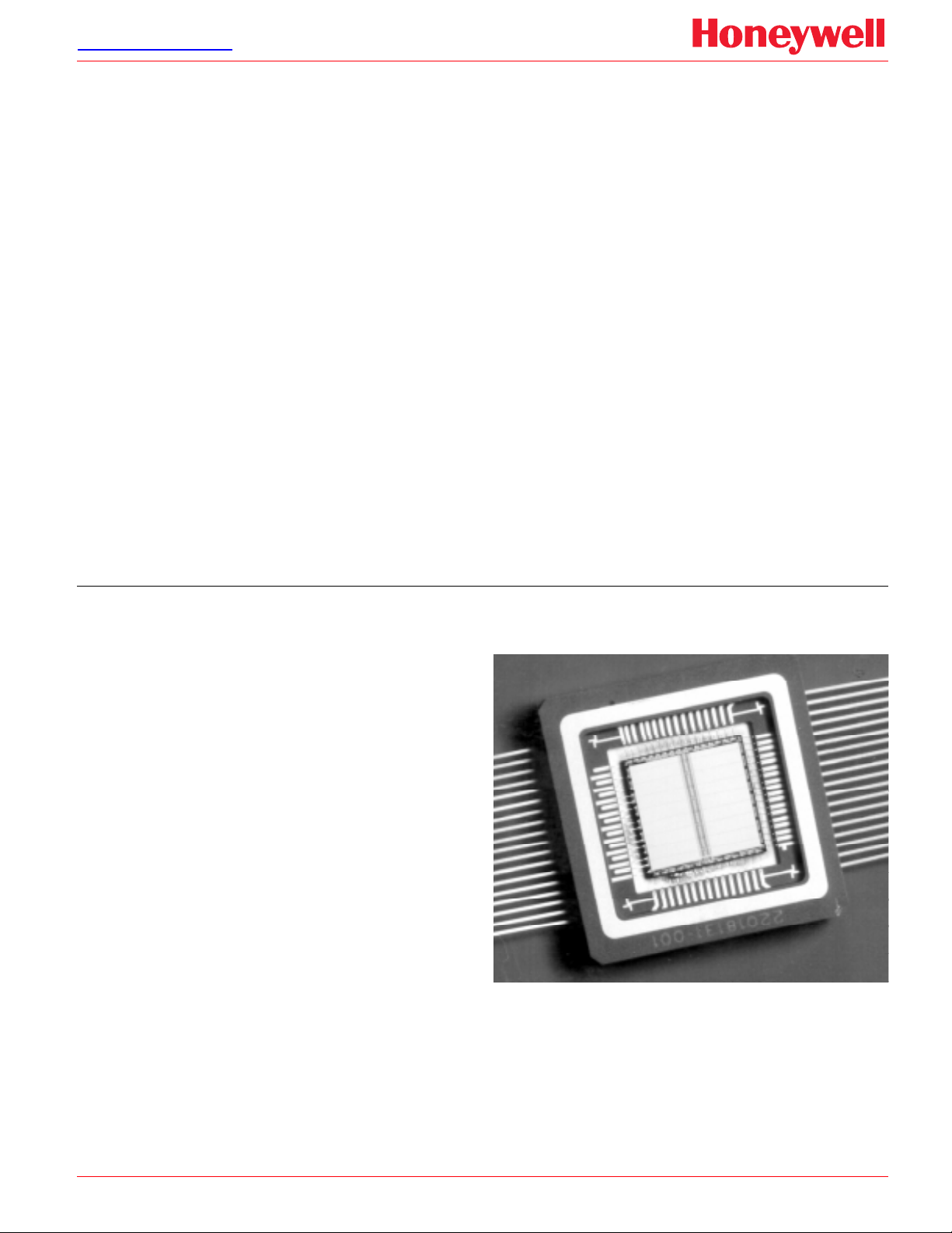
32K x 8 STATIC RAM—SOI HX6356
FEATURES
RADIATION
• Fabricated with RICMOS™ IV Silicon on Insulator (SOI)
0.75 µm Process (L
= 0.6 µm)
eff
• Total Dose Hardness through 1x10⁶rad(SiO2)
• Neutron Hardness through 1x1014 cm
-2
• Dynamic and Static Transient Upset Hardness
through 1x10¹¹ rad(Si)/s
12
• Dose Rate Survivability through 1x10
• Soft Error Rate of <1x10
-10
upsets/bit-day
rad(Si)/s
in Geosynchronous Orbit
• Latchup Free
GENERAL DESCRIPTION
The 32K x 8 Radiation Hardened Static RAM is a high
performance 32,768 word x 8-bit static random access
memory with industry-standard functionality. It is fabricated
with Honeywell’s radiation hardened technology, and is
designed for use in systems operating in harsh, transient
radiation environments. The RAM operates over the full
military temperature range and requires only a single 5 V ±
10% power supply. The RAM is available with either TTL or
CMOS compatible I/O. Power consumption is typically less
than 15 mW/MHz in operation, and less than 5 mW when
de-selected. The RAM read operation is fully asynchronous, with an associated typical access time of 14 ns at 5V.
OTHER
• Listed On SMD# 5962-95845
• Fast Read/Write Cycle Times
≤ 17 ns (Typical)
≤ 25 ns (-55 to 125°C)
• Typical Operating power < 15 mW/MHz
• Asynchronous Operation
• CMOS or TTL Compatible I/O
• Single 5 V ± 10% Power Supply
• Packaging Options
- 36-Lead CFP—Bottom Braze (0.630 in. x 0.650 in.)
- 36-Lead CFP—Top Braze (0.630 in. x 0.650 in.)
Honeywell’s enhanced SOI RICMOS™IV (Radiation Insensitive CMOS) technology is radiation hardened through the
use of advanced and proprietary design, layout and process hardening techniques. The RICMOS™ IV process is a
5-volt, SIMOX CMOS technology with a 150 Å gate oxide
and a minimum drawn feature size of 0.75 µm (0.6 µm
effective gate length—L
). Additional features include
eff
tungsten via plugs, Honeywell’s proprietary SHARP planarization process, and a lightly doped drain (LDD) structure for improved short channel reliability. A 7 transistor
(7T) memory cell is used for superior single event upset
hardening, while three layer metal power bussing and the
low collection volume SIMOX substrate provide improved
dose rate hardening.
HX6356
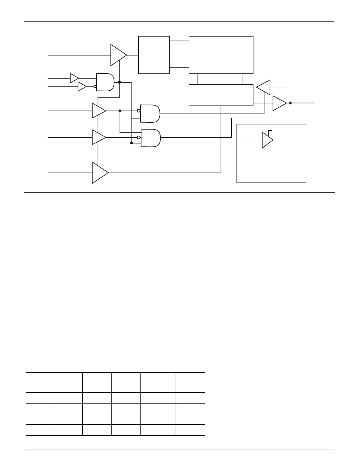
FUNCTIONAL DIAGRAM
A:0-8,12-13
CE
NCS
NWE
NOE
A:9-11, 14
SIGNAL DEFINITIONS
32,768 x 8
Memory
Array
• • •
Column Decoder
Data Input/Output
8
DQ:0-7
11
Row
Decoder
•
•
•
8
WE • CS • CE
NWE • CS • CE • OE
(0 = high Z)
Signal
1 = enabled
Signal
#
All controls must be
enabled for a signal to
4
pass. (#: number of
buffers, default = 1)
A: 0-14 Address input pins which select a particular eight-bit word within the memory array.
DQ: 0-7 Bidirectional data pins which serve as data outputs during a read operation and as data inputs during a write
operation.
NCS Negative chip select, when at a low level allows normal read or write operation. When at a high level NCS
forces the SRAM to a precharge condition, holds the data output drivers in a high impedance state and
disables all input buffers except CE. If this signal is not used it must be connected to VSS.
NWE Negative write enable, when at a low level activates a write operation and holds the data output drivers in a
high impedance state. When at a high level NWE allows normal read operation.
NOE Negative output enable, when at a high level holds the data output drivers in a high impedance state. When
at a low level, the data output driver state is defined by NCS, NWE and CE. If this signal is not used it must
be connected to VSS.
CE Chip enable, when at a high level allows normal operation. When at a low level CE forces the SRAM to a
precharge condition, holds the data output drivers in a high impedance state and disables all the input buffers
except the NCS input buffer. If this signal is not used it must be connected to VDD.
TRUTH TABLE
NCS CE NWE NOE MODE DQ
L H H L Read Data Out
L H L X Write Data In
H X XX XX Deselected High Z
X L XX XX Disabled High Z
Notes:
X: VI=VIH or VIL
XX: VSS≤VI≤VDD
NOE=H: High Z output state maintained for
NCS=X, CE=X, NWE=X
2
RADIATION CHARACTERISTICS
HX6356
Total Ionizing Radiation Dose
The SRAM will meet all stated functional and electrical
specifications over the entire operating temperature range
after the specified total ionizing radiation dose. All electrical
and timing performance parameters will remain within
specifications after rebound at VDD = 5.5 V and T =125°C
extrapolated to ten years of operation. Total dose hardness
is assured by wafer level testing of process monitor transistors and RAM product using 10 keV X-ray and Co60
radiation sources. Transistor gate threshold shift correlations have been made between 10 keV X-rays applied at a
dose rate of 1x10⁵ rad(SiO2)/min at T = 25°C and gamma
rays (Cobalt 60 source) to ensure that wafer level X-ray
testing is consistent with standard military radiation test
environments.
Transient Pulse Ionizing Radiation
The SRAM is capable of writing, reading, and retaining
stored data during and after exposure to a transient
ionizing radiation pulse up to the transient dose rate upset
specification, when applied under recommended operating conditions. To ensure validity of all specified performance parameters before, during, and after radiation
(timing degradation during transient pulse radiation (timing degradation during transient pulse radiation is ≤10%),
it is suggested that stiffening capacitance be placed on or
near the package VDD and VSS, with a maximum inductance between the package (chip) and stiffening capacitance of 0.7 nH per part. If there are no operate-through
or valid stored data requirements, typical circuit board
mounted de-coupling capacitors are recommended.
The SRAM will meet any functional or electrical specification after exposure to a radiation pulse up to the transient
dose rate survivability specification, when applied under
recommended operating conditions. Note that the current
conducted during the pulse by the RAM inputs, outputs,
and power supply may significantly exceed the normal
operating levels. The application design must accommodate these effects.
Neutron Radiation
The SRAM will meet any functional or timing specification
after exposure to the specified neutron fluence under
recommended operating or storage conditions. This assumes an equivalent neutron energy of 1 MeV.
Soft Error Rate
The SRAM has an extremely low Soft Error Rate (SER) as
specified in the table below. This hardness level is defined
by the Adams 90% worst case cosmic ray environment.
The low SER is achieved by the use of a unique 7-transistor
memory cell and the oxide isolation of the SOI substrate.
Latchup
The SRAM will not latch up due to any of the above radiation
exposure conditions when applied under recommended
operating conditions. Fabrication with the SIMOX substrate
material provides oxide isolation between adjacent PMOS
and NMOS transistors and eliminates any potential SCR
latchup structures. Sufficient transistor body tie connections to the p- and n-channel substrates are made to ensure
no source/drain snapback occurs.
RADIATION HARDNESS RATINGS (1)
Parameter
Total Dose ≥1x10
Transient Dose Rate Upset ≥1x10
Transient Dose Rate Survivability ≥1x10
Soft Error Rate <1x10
Neutron Fluence ≥1x10
(1) Device will not latch up due to any of the specified radiation exposure conditions.
(2) Operating conditions (unless otherwise specified): VDD=4.5 V to 5.5 V, -55°C to 125°C.
Limits (2) Test Conditions
6
11
12
-10
14
3
Units
rad(SiO2)
rad(Si)/s
rad(Si)/s
upsets/bit-day
2
N/cm
TA=25°C
Pulse width ≤1 µs
Pulse width ≤50 ns, X-ray,
VDD=6.0 V, T
TA=125°C, Adams 90%
worst case environment
1 MeV equivalent energy,
Unbiased, T
A=25°C
A=25°C

HX6356
ABSOLUTE MAXIMUM RATINGS (1)
Rating
Symbol
Parameter
Min
Max
Units
VDD Positive Supply Voltage (2) -0.5 6.5 V
VPIN Voltage on Any Pin (2) -0.5 VDD+0.5 V
TSTORE Storage Temperature (Zero Bias) -65 150 °C
TSOLDER Soldering Temperature (5 Seconds) 270 °C
PD Total Package Power Dissipation (3) 2.0 W
IOUT DC or Average Output Current 25 mA
VPROT ESD Input Protection Voltage (4) 2000 V
ΘJC Thermal Resistance (Jct-to-Case) – 36 FP 2 °C/W
TJ Junction Temperature 175 °C
(1) Stresses in excess of those listed above may result in permanent damage. These are stress ratings only, and operation at these levels is not
implied. Frequent or extended exposure to absolute maximum conditions may affect device reliability.
(2) Voltage referenced to VSS.
(3) RAM power dissipation (IDDSB + IDDOP) plus RAM output driver power dissipation due to external loading must not exceed this specification.
(4) Class 2 electrostatic discharge (ESD) input protection. Tested per MIL-STD-883, Method 3015 by DESC certified lab.
RECOMMENDED OPERATING CONDITIONS
Symbol
Parameter
Min
MaxTyp
VDD Supply Voltage (referenced to VSS) 4.5 5.0 5.5 V
TA Ambient Temperature -55 25 125 °C
VPIN Voltage on Any Pin (referenced to VSS) -0.3 VDD+0.3 V
CAPACITANCE (1)
Description
Symbol
Parameter
Typical
(1)
CI Input Capacitance 7 pF VI=VDD or VSS, f=1 MHz
CO Output Capacitance 9 pF VIO=VDD or VSS, f=1 MHz
(1) This parameter is tested during initial design characterization only.
Worst Case
Min
Max
Units
Test Conditions
DATA RETENTION CHARACTERISTICS
Symbol
Parameter
Typical
(1)
Worst Case
Min
VDR Data Retention Voltage 2.5 V
IDR Data Retention Current
(1) Typical operating conditions: TA= 25°C, pre-radiation.
(2) Worst case operating conditions: -55°C to +125°C, post total dose at 25°C.
(2)
Units
Test Conditions
Max
NCS=VDR
VI=VDR or VSS
500 µA NCS=VDD=2.5V, VI=VDD or VSS
330 µA NCS=VDD=3.0V, VI=VDD or VSS
Units
4
 Loading...