

Hitachi HDP725016GLAT80, CINEMASTAR P7K500, HDP725016GLA380, HDP725025GLAT80, HDP725025GLA380/1 Specification
...Page 1
Hitachi Global Storage Technologies
Hard Disk Drive Specification
Hitachi Deskstar P7K500
Hitachi CinemaStar P7K500
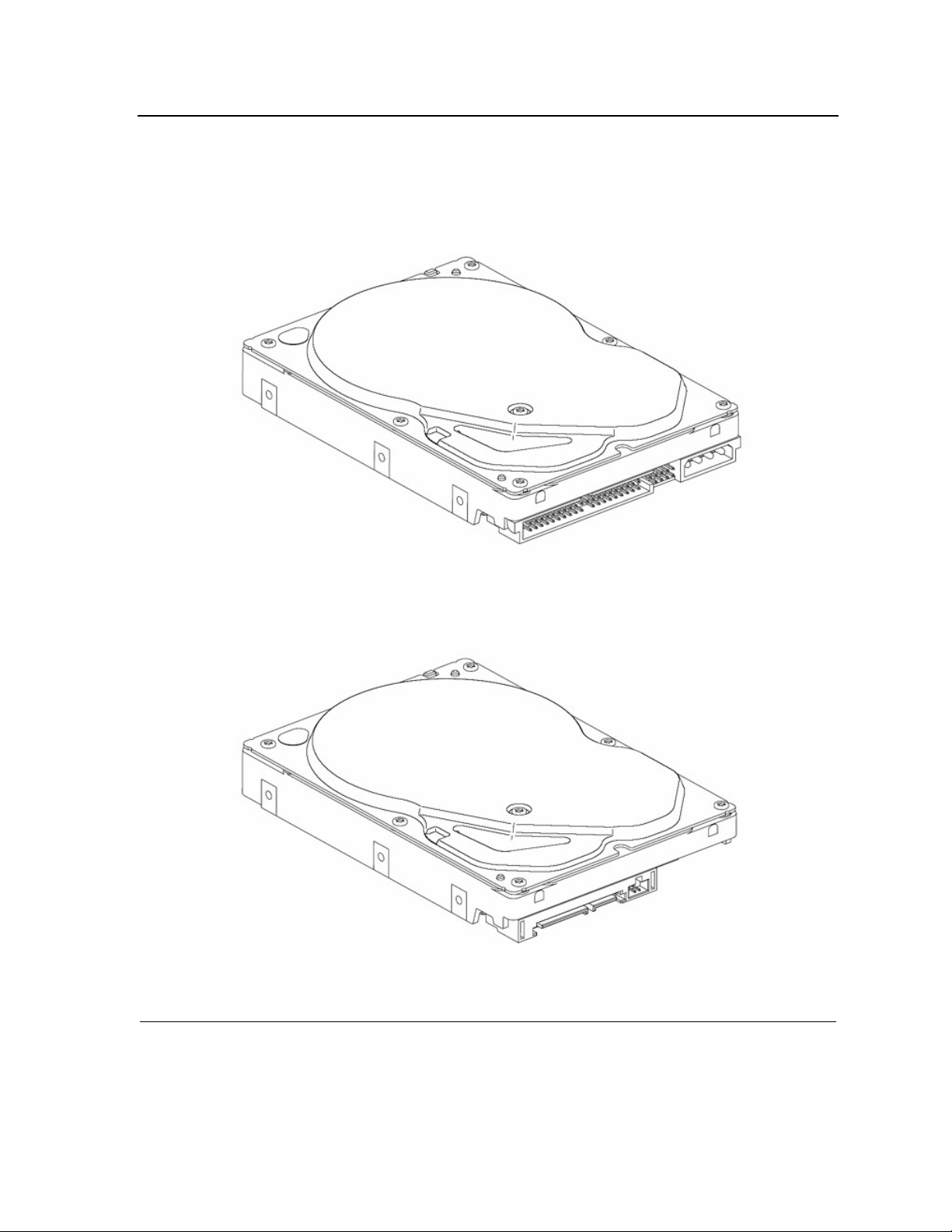
3.5 inch hard disk drive
Models: HDP725016GLAT80
HDP725016GLA380
HDP725025GLAT80
HDP725025GLA380/1
HDP725032GLAT80
HDP725032GLA380
HDP725032GLA360/1
HDP725040GLAT80
HDP725040GLA380
HDP725040GLA360/1
HDP725050GLAT80
HDP725050GLA380
HDP725050GLA360/1
HCP725016GLAT80
HCP725016GLA380
HCP725025GLAT80
HCP725025GLA380
HCP725032GLAT80
HCP725032GLA380
HCP725050GLAT80
HCP725050GLA380
Page 2

Revision 1.0 (November 14, 2007)
The following paragraph does not apply to the United Kingdom or an y coun tr y wh ere suc h provisi on s are
inconsistent with local law: HITACHI GLOBAL STORAGE TECHNOLOGIES Inc. PROVIDES THIS
PUBLICATION “AS IS” WITHOUT WARRANTY OF ANY KIND, EITHER EXPRESS OR IMPLIED,
INCLUDING, BUT NOT LIMITED TO, THE IMPLIED WARRANTIES OF MERCHANTABILITY OR
FITNESS FOR A PARTICULAR PURPOSE. Some states do not allow disclaimer or express or implied
warranties in certain transactions, t herefore, this statement may not apply to you.
This publication could include technical inaccuracies or typographical errors. Changes are periodically made to
the information herein; these changes will be incorporated in new editions of the publication. Hitachi Global
Storage Technologies may make improvem ents or changes in any products or programs described in this
publication at any time.
It is possible that this publication may contain reference to, or information about, Hitachi Global Storage
Technologies products (machines and program s), programm ing, or servic es that are not announce d in your
country. Such references or information must not be construed to mean that Hitachi G lobal Storage Technologies
intends to announce such Hitachi Global Storage Technologies products, programming, or services in your
country.
Technical information about this product is available by contacting yo ur local Hitachi Global Storage
Technologies representative or on the
|Internet at
http://www.HitachiGST.com/
Hitachi Global Storage Technologies may have patents or pending patent applications covering subject matter in
this document. The furnishing of this document does not give you any lice nse to these patents. You can send
license inquiries in writing to the Hitachi Global Storage Technologies Director of Commercial Relations,
Hitachi Global Storage Technologies Inc. , San Jose, CA .
©Copyright Hitachi Global Storage Tech nologies 2004. All rights reserved.
Note to U.S. Government Users —Docume ntation related to restricted rights —Use, duplication or disclosure is
subject to restrictions set forth in GSA ADP Schedule Contract with Hitachi Global Storage Technologies Inc.
HITACHI Deskstar & CinemaStar P7K500 Hard Disk Drive specification (Rev 1.1)
i
Page 3

Table of contents
1.0 General.................................. .................................................................................................................. 2
1.1 Introduction.............................................................................................................................. 2
1.2 Glossary.................................................................................................................................... 2
1.3 Caution ..................................................................................................................................... 2
1.4 References ................................................................................................................................ 2
2.0 General features...... ....................................................................................................................... ......... 3
Part 1. Functional specification ................................................................................................................ 5
3.0 Fixed disk subsystem description............ .................................................. .............................................. 7
3.1 Control Electronics .................................................................................................................. 7
3.2 Head disk assembly ................................................................................................................. 7
3.3 Actuator.................................................................................................................................... 7
4.0 Drive characteristics................................................................................................................................ 8
4.1 Default logical drive parameters............................................................................................. 8
PP
4.2
Data sheet ................................................................................................................................ 9
4.3 World Wide Name Assignment................................................................................................ 9
4.4 Drive organization ................................................................................................................... 9
4.5 Performance characteristics.................................................................................................. 10
5.0 Defect flagging strategy......................................................................................................................... 14
5.1 Electrical interface................................................................................................................. 15
5.2 Signal timings ........................................................................................................................ 22
5.3 Jumper settings(PATA model)............................................................................................... 35
5.4 Environment .......................................................................................................................... 41
5.5 DC power requirements......................................................................................................... 43
5.6 Reliability............................................................................................................................... 46
5.7 Mechanical specifications ...................................................................................................... 47
5.8 Vibration and shock............................................................................................................... 52
5.9 Acoustics................................................................................................................................. 54
5.10 Identification labels ............................................................................................................... 54
5.11 Safety...................................................................................................................................... 55
5.12 Electromagnetic compatibility............................................................................................... 56
Part 2. Interface Specification................................................................................................................. 57
6.0 General.................................. ................................................................................................................ 58
6.1 Introduction............................................................................................................................ 58
6.2 Terminology............................................................................................................................ 58
6.3 Deviations From Standard ....................................................................................................58
7.0 Registers............................................................................................................................................... 59
7.1 Alternate Status Register...................................................................................................... 59
7.2 Command register.................................................................................................................. 59
7.3 Cylinder High Register.......................................................................................................... 59
7.4 Cylinder Low Register ........................................................................................................... 59
7.5 Data Register ......................................................................................................................... 60
7.6 Device Control Register......................................................................................................... 60
7.7 Drive Address Register.......................................................................................................... 60
7.8 Device/Head Register............................................................................................................. 61
7.9 Error Register ........................................................................................................................ 62
7.10 Features Register................................................................................................................... 62
7.11 Sector Count Register............................................................................................................ 62
7.12 Sector Number Register ........................................................................................................ 62
7.13 Status Register....................................................................................................................... 62
8.0 General Operation Descriptions............................................................................................................. 64
8.1 Reset Response....................................................................................................................... 64
8.2 Diagnostic and Reset considerations .................................................................................... 65
8.3 Sector Addressing Mode......................................................................................................... 66
8.4 Power Management Feature ................................................................................................. 67
8.5 SMART Function ................................................................................................................... 68
8.6 Security Mode Feature Set.................................................................................................... 70
HITACHI Deskstar & CinemaStar P7K500 Hard Disk Drive specification (Rev 1.1)
ii
Page 4

8.7 Host Protected Area Feature.................................................................................................76
8.8 Seek Overlap .......................................................................................................................... 78
8.9 Write Cache Function ............................................................................................................ 78
8.10 Reassign Function.................................................................................................................. 79
8.11 Power-up in Standby feature set........................................................................................... 80
8.12 Advanced Power Management feature set (APM)................................................................ 80
8.13 Automatic Acoustic Management feature set (AAM)........................................................... 81
8.14 Address Offset Feature.......................................................................................................... 81
8.15 48-bit Address Feature Set.................................................................................................... 83
8.16 Streaming feature Set............................................................................................................ 84
8.17 SATA BIST (Built-in Self Test).............................................................................................. 86
8.18 SATA Interface Power Management..................................................................................... 86
8.19 Software Setting Preservation ..............................................................................................87
8.20 SATA II Optional Features.................................................................................................... 88
8.21 SCT Command Transport feature Set .................................................................................. 92
9.0 Command Protocol...............................................................................................................................111
9.1 PIO Data In commands ........................................................................................................ 111
9.2 PIO Data Out commands......................................................................................................111
9.3 Non-Data commands ............................................................................................................112
9.4 DMA Data In commands and DMA Data Out commands...................................................112
9.5 First-party DMA commands.................................................................................................113
10.0 Command Descriptions........................................................................................................................115
10.1 Check Power Mode (E5h/98h) ..............................................................................................119
10.2 ...................................................................................................................................................119
10.3 Configure Stream (51h) ........................................................................................................120
10.4 Device Configuration Overlay (B1h)....................................................................................122
10.5 Download Microcode (92h)....................................................................................................126
10.6 Execute Device Diagnostic (90h)..........................................................................................128
10.7 Flush Cache (E7h).................................................................................................................129
10.8 Flush Cache Ext (EAh) .........................................................................................................130
10.9 Format Track (50h)...............................................................................................................131
10.10 Format Unit (F7h).............................................................................................................133
10.11 Identify Device (ECh)........................................................................................................134
10.12 Idle (E3h/97h)....................................................................................................................145
10.13 Idle Immediate (E1h/95h) .................................................................................................147
10.14 Initialize Device Parameters (91h)...................................................................................148
10.15 Read Buffer (E4h)..............................................................................................................149
10.16 Read DMA(C8h/C9h).........................................................................................................150
10.17 Read DMA Ext (25h) .........................................................................................................152
10.18 Read FPDMA Queued (60h)..............................................................................................154
10.19 Read Log Ext (2Fh) ...........................................................................................................156
10.20 Read Multiple (C4h) ..........................................................................................................169
10.21 Read Multiple Ext (29h)....................................................................................................170
10.22 Read Native Max Address (F8h).......................................................................................172
10.23 Read Native Max Address Ext (27h) ................................................................................173
10.24 Read Sector(s) (20h/21h) ...................................................................................................175
10.25 Read Sector(s) Ext (24h)....................................................................................................177
10.26 Read Stream DMA (2Ah)...................................................................................................179
10.27 Read Stream PIO (2Bh) ....................................................................................................182
10.28 Read Verify Sector(s) (40h/41h) ........................................................................................184
10.29 Read Verify Sector(s) Ext (42h).........................................................................................186
10.30 Recalibrate (1xh) ...............................................................................................................188
10.31 Security Disable Password (F6h)......................................................................................189
10.32 Security Erase Prepare (F3h) ...........................................................................................191
10.33 Security Erase Unit (F4h).................................................................................................192
10.34 Security Freeze Lock (F5h) ...............................................................................................194
10.35 Security Set Password (F1h).............................................................................................195
10.36 Security Unlock (F2h) .......................................................................................................197
HITACHI Deskstar & CinemaStar P7K500 Hard Disk Drive specification (Rev 1.1)
iii
Page 5

10.37 Seek (7xh) ..........................................................................................................................199
10.38 Set Features (EFh)............................................................................................................200
10.39 Set Max Address (F9h)......................................................................................................205
10.40 Set Max Address Ext (37h) ...............................................................................................211
10.41 Set Multiple (C6h).............................................................................................................213
10.42 Sleep (E6h/99h) .................................................................................................................214
10.43 SMART Function Set (B0h) ..............................................................................................215
10.44 Standby (E2h/96h).............................................................................................................233
10.45 Standby Immediate (E0h/94h)..........................................................................................235
10.46 Write Buffer (E8h).............................................................................................................236
10.47 Write DMA (Cah/CBh).......................................................................................................237
10.48 Write DMA FUA Ext (3Dh) ...............................................................................................239
10.49 Write DMA Ext (35h).........................................................................................................241
10.50 Write FPDMA Queued (61h).............................................................................................243
10.51 Write Log Ext (3Fh)...........................................................................................................245
10.52 Write Multiple (C5h) .........................................................................................................247
10.53 Write Multiple Ext (39h)...................................................................................................249
10.54 Write Multiple FUA Ext (CEh) .........................................................................................251
10.55 Write Sector(s) (30h/31h) ..................................................................................................253
10.56 Write Sector(s) Ext (34h)...................................................................................................255
10.57 Write Stream DMA (3Ah)..................................................................................................257
10.58 Write Stream PIO (3Bh)....................................................................................................260
10.59 Write Uncorrectable Ext (45h)..........................................................................................263
11.0 Timings................................................................................................................................................ 266
HITACHI Deskstar & CinemaStar P7K500 Hard Disk Drive specification (Rev 1.1)
iv
Page 6

List of tables
Table 1 Formatted capacity................................................................................................................ 8
Table 2 Mechanical positioning performance ................................................................................. 9
Table 3 World Wide Name Assignment ........................................................................................... 9
Table 4 Command overhead .......................................................................................................... 10
Table 5 Mechanical positioning performance ................................................................................11
Table 6 Full stroke seek time .........................................................................................................11
Table 7 Single Track Seek Time .....................................................................................................11
Table 8 Latency Time..................................................................................................................... 12
Table 9 Drive ready time ............................................................................................................... 12
Table 10 Mode transition times..................................................................................................... 13
Table 11 Table of signals................................................................................................................ 17
Table 12 Signal special definitions for Ultra DMA....................................................................... 17
Table 13 Interface connector pins and I/O signals........................................................................ 20
Table 14 Parameter descriptions................................................................................................... 21
Table 15 System reset timing ........................................................................................................ 22
Table 16 PIO cycle timings ............................................................................................................ 23
Table 17 Multiword DMA cycle timings........................................................................................ 25
Table 18 Ultra DMA cycle timings (Initiating Read) ................................................................... 26
Table 19 Ultra DMA cycle timings (Host pausing Read) ............................................................. 27
Table 20 Ultra DMA cycle timings (Host terminating Read)....................................................... 28
Table 21 Ultra DMA cycle timings (Device Terminating Read)................................................... 29
Table 22 Ultra DMA cycle timings (Initiating Write)................................................................... 30
Table 23 Ultra DMA cycle timings (Device Pausing Write)......................................................... 31
Table 24 Ultra DMA cycle timings (Device terminating Write)................................................... 32
Table 25 Ultra DMA cycle timings (Host Terminating Write)..................................................... 33
Table 26 I/O address map .............................................................................................................. 34
Table 27 Temperature and humidity ............................................................................................ 41
Table 28 Input voltage ................................................................................................................... 43
Table 29 Power supply current of 2 Disk PATA models............................................................... 43
Table 30 Power supply current of 1 Disk PATA models............................................................... 44
Table 31 Power supply current of 2 Disk SATA models............................................................... 44
Table 32 Power supply current of 1 Disk SATA models............................................................... 45
Table 33 Power supply generated ripple at drive power connector ............................................. 45
Table 34 Physical Dimensions ....................................................................................................... 48
Table 35 Random vibration PSD profile break points (operating)............................................... 52
Table 36 Random vibration PSD profile break points (nonoperating)......................................... 52
Table 37 Sinusoidal shock wave .................................................................................................... 53
Table 38 Rotational Shock ............................................................................................................. 53
Table 39 Sound power levels.......................................................................................................... 54
Table 40 Alternate Status Register ............................................................................................... 59
Table 41 Device Control Register .................................................................................................. 60
Table 42 Drive Address Register ................................................................................................... 60
Table 43 Device/Head Register...................................................................................................... 61
Table 44 Error Register ................................................................................................................. 62
Table 45 Status Register................................................................................................................ 63
Table 46 Reset Response................................................................................................................ 64
Table 47 Default Register Values.................................................................................................... 65
Table 48 Diagnostic Codes ............................................................................................................. 65
Table 49 Power conditions.............................................................................................................. 68
Table 50 Command table for device lock operation - 1................................................................. 74
Table 51 Command table for device lock operation - 2................................................................. 75
Table 52 Phy Event Counter Identifiers........................................................................................... 89
Table 53 READ LOG EXT Log Page 11h data structure definition............................................. 90
Table 54 SCT Log Page and direction............................................................................................. 92
HITACHI Deskstar & CinemaStar P7K500 Hard Disk Drive specification (Rev 1.1)
v
Page 7

Table 55 Identify Device Information Word 206........................................................................... 92
Table 56 Output Registers of SCT Command Using SMART ...................................................... 93
Table 57 Input Registers of SCT Command Using SMART......................................................... 93
Table 58 Input Registers of SCT Command Using Write Log Ext............................................... 94
Table 59 Output Registers of SCT Command Using Write Log Ext ............................................ 94
Table 60 Key Sector Format............................................................................................................ 95
Table 61 SCT Action Code List........................................................................................................ 95
Table 62 Extended Status Code...................................................................................................... 96
Table 63 Input Registers of SCT Data Transfer Using SMART .................................................. 97
Table 64 Input Registers of SCT Data Transfer using Read/Write Log Ext................................ 97
Table 65 Intput Registers of SCT Status Request Using SMART............................................... 98
Table 66 Input Registers of SCT Status Request Using Read Log Ext ....................................... 98
Table 67 Data Format of SCT Status Response...........................................................................100
Table 68 LBA Segment Access (Inputs)........................................................................................101
Table 69 LBA Segment Access (Outputs).....................................................................................101
Table 70 Error Recovery Control command (Inputs)...................................................................104
Table 71 Error Recovery Control command (Onputs) .................................................................104
Table 72 Feature Control command (Inputs)...............................................................................105
Table 73 Feature Control command (Outputs)............................................................................105
Table 74 Feature Code List............................................................................................................106
Table 75 SCT Data Table command (Inputs)...............................................................................107
Table 76 SCT Data Table command (Outputs) ............................................................................107
Table 77 Table ID ...........................................................................................................................107
Table 78 Data Format of HDA Absolute Temperature History Table.........................................109
Table 79 Command Set..................................................................................................................115
Table 80 Command Set --Continued--............................................................................................116
Table 81 Command Set (Subcommand ) ........................................................................................117
Table 82 Check Power Mode Command (E5h/98h)......................................................................119
Table 83 Configure Stream Command (51h)..................................................................................120
Table 84 Device Configuration Overlay Command (B1h) ...........................................................122
Table 85 Device Configuration Overlay Features register values..............................................122
Table 86 Device Configuration Overlay Data structure..............................................................124
Table 87 DCO error information definition......................................................................................125
Table 88 Download Microcode Command (92h)S ...........................................................................126
Table 89 Execute Device Diagnostic Command (90h) .................................................................128
Table 90 Flush Cache Command (E7h).........................................................................................129
Table 91 Flush Cache Ext Command (EAh)...................................................................................130
Table 92 Format Track Command(50h) .......................................................................................131
Table 93 Format Unit Command (F7h )...........................................................................................133
Table 94 Identify Device Command (ECh) .....................................................................................134
Table 95 Identify device information............................................................................................135
Table 96 Identify device information --Continued--.....................................................................136
Table 97 Identify device information --Continued— ...................................................................137
Table 98 Identify device information --Continued--.....................................................................138
Table 99 Identify device information --Continued--.....................................................................139
Table 100 Identify device information --Continued--...................................................................140
Table 101 Identify device information --Continued--...................................................................141
Table 102 Identify device information --Continued--...................................................................142
Table 103 Identify device information --Continued--...................................................................143
Table 104 Identify device information --Continued--...................................................................144
Table 105 Idle Command (E3h/97h)...............................................................................................145
Table 106 Idle Immediate Command (E1h/95h).............................................................................147
Table 107 Initialize Device Parameters Command (91h)............................................................148
Table 108 Read Buffer Command (E4h) ........................................................................................149
Table 109 Read DMA Command (C8h/C9h)..................................................................................150
Table 110 Read DMA Ext Command (25h)....................................................................................152
Table 111 Read FPDMA Queued Command (60h) ........................................................................154
Table 112 Read Log Ext Command (2Fh)......................................................................................156
HITACHI Deskstar & CinemaStar P7K500 Hard Disk Drive specification (Rev 1.1)
vi
Page 8

Table 113 Log Address Definition...................................................................................................157
Table 114 General Purpose Log Directory .....................................................................................158
Table 115 Extended Comprehensive SMART Error Log.............................................................159
Table 116 Extended Error log data structure..................................................................................160
Table 117 Command data structure ...............................................................................................160
Table 118 Error data structure........................................................................................................161
Table 119 Extended Self-test log data structure..........................................................................162
Table 120 Extended Self-test log descriptor entry.......................................................................163
Table 121 Command Error information..........................................................................................164
Table 122 Read Stream Error Log................................................................................................165
Table 123 Stream Error Log entry ...............................................................................................166
Table 124 Write Stream Error Log...............................................................................................167
Table 125 Streaming Performance Parameters log.....................................................................168
Table 126 Sector Time Array Entry (Linearly Interpolated).......................................................168
Table 127 Position Array Entry (Linearly Interpolated).............................................................168
Table 128 Access Time Array Entry (Linearly Interpolated)......................................................168
Table 129 Read Multiple Command (C4h).....................................................................................169
Table 130 Read Multiple Ext Command (29h)................................................................................170
Table 131 Read Native Max ADDRESS (F8h) ...............................................................................172
Table 132 Read Native Max Address Ext (27h) .............................................................................173
Table 133 Read Sector(s) Command (20h/21h).............................................................................175
Table 134 Read Sector(s) Ext Command (24h) .............................................................................177
Table 135 Read Stream DMA Command (2Ah) ...........................................................................179
Table 136 Read Stream PIO Command (2Bh) .............................................................................182
Table 137 Read Verify Sector(s) Command (40h/41h).................................................................184
Table 138 Read Verify Sector(s) Ext Command (42h).................................................................186
Table 139 Recalibrate Command (1xh)..........................................................................................188
Table 140 Security Disable Password Command (F6h) ..............................................................189
Table 141 Password Information for Security Disable Password command ..............................190
Table 142 Security Erase Prepare Command (F3h)....................................................................191
Table 143 Security Erase Unit Command (F4h).............................................................................192
Table 144 Erase Unit Information...................................................................................................193
Table 145 Security Freeze Lock Command (F5h)..........................................................................194
Table 146 Security Set Password Command (F1h) .....................................................................195
Table 147 Security Set Password Information................................................................................196
Table 148 Security Unlock Command (F2h)...................................................................................197
Table 149 Security Unlock Information...........................................................................................198
Table 150 Seek Command (7xh)....................................................................................................199
Table 151 Set Features Command (EFh).......................................................................................200
Table 152 Set Max ADDRESS (F9h)..............................................................................................205
Table 153 Set Max set Password...................................................................................................207
Table 154 Set Max Set Password data contents............................................................................207
Table 155 Set Max Lock.................................................................................................................208
Table 156 Set Max Unlock (F9h)....................................................................................................209
Table 157 Set Max Freeze Lock (F9h)...........................................................................................210
Table 158 Set Max Address Ext Command (37h) ..........................................................................211
Table 159 Set Multiple Command (C6h) ........................................................................................213
Table 160 Sleep Command (E6h/99h)...........................................................................................214
Table 161 SMART Function Set Command (B0h)..........................................................................215
Table 162 Log sector addresses ....................................................................................................218
Table 163 Device Attribute Data Structure.....................................................................................220
Table 164 Individual Attribute Data Structure...........................................................................221
Table 165 Device Attribute Thresholds Data Structure..............................................................225
Table 166 Individual Threshold Data Structure .........................................................................225
Table 167 SMART Log Directory....................................................................................................226
Table 168 SMART summary error log sector.................................................................................227
Table 169 Error log data structure..................................................................................................228
Table 170 Command data structure ...............................................................................................228
HITACHI Deskstar & CinemaStar P7K500 Hard Disk Drive specification (Rev 1.1)
vii
Page 9

Table 171 Error data structure........................................................................................................229
Table 172 Self-test log data structure.............................................................................................230
Table 173 Selective self-test log data structure...........................................................................231
Table 174 Selective self-test feature flags....................................................................................231
Table 175 SMART Error Codes......................................................................................................232
Table 176 Standby Command (E2h/96h).......................................................................................233
Table 177 Standby Immediate Command (E0h/94h)...................................................................235
Table 178 Write Buffer Command (E8h) ........................................................................................236
Table 179 Write DMA Command (Cah/CBh)..................................................................................237
Table 180 Write DMA FUA Ext Command (3Dh) ...........................................................................239
Table 181 Write DMA Ext Command (35h)....................................................................................241
Table 182 Write FPDMA Queued Command (61h)........................................................................243
Table 183 Write Log Ext Command (3Fh)......................................................................................245
Table 184 Write Multiple Command (C5h) .....................................................................................247
Table 185 Write Multiple Ext Command (39h)................................................................................249
Table 186 Write Multiple FUA Ext Command (CEh)..................................................................251
Table 187 Write Sector(s) Command (30h/31h).............................................................................253
Table 188 Write Sector(s) Ext Command (34h)..............................................................................255
Table 189 Write Stream DMA Command (3Ah)...........................................................................257
Table 190 Write Stream PIO Command (3Bh) ............................................................................260
Table 191 Write Uncorrectable Ext Command (45h)...................................................................263
Table 192 Timeout Values ............................................................................................................266
HITACHI Deskstar & CinemaStar P7K500 Hard Disk Drive specification (Rev 1.1)
viii
Page 10

List of figures
Figure 1 PList physical format............................................................................................................. 14
Figure 2 Connector location (PATA)..................................................................................................... 15
Figure 3 Connector location (SATA).................................................................................................... 15
Figure 4 Power connector pin assignments............................................................................................ 16
Figure 5 the timing of COMRESET, COMINIT and COMWAKE.......................................................... 21
Figure 6 System reset timing chart....................................................................................................... 22
Figure 7 PIO cycle timings chart.......................................................................................................... 23
Figure 8 Multiword DMA cycle timing chart ........................................................................................ 25
Figure 9 Ultra DMA cycle timing chart (Initiating Read)........................................................................ 26
Figure 10 Ultra DMA cycle timing chart (Host pausing Read)................................................................ 27
Figure 11 Ultra DMA cycle timing chart (Host terminating Read)........................................................... 28
Figure 12 Ultra DMA cycle timing chart (Device terminating Read)....................................................... 29
Figure 13 Ultra DMA cycle timing chart (Initiating Write)..................................................................... 30
Figure 14 Ultra DMA cycle timing chart (Device Pausing Write)............................................................ 31
Figure 15 Ultra DMA cycle tim ing chart (Device Terminating Write) ..................................................... 32
Figure 16 Ultra DMA cycle timing chart (Host Terminating Write)......................................................... 33
Figure 17 Jumper pin location............................................................................................................. 35
Figure 18 Jumper pin identification...................................................................................................... 35
Figure 19 Jumper positions for normal use............................................................................................ 37
Figure 20 Jumper positions for 15 logical head default........................................................................... 38
Figure 21 Jumper positions for capacity clip to 32GB............................................................................ 39
Figure 22 Jumper settings for Disabling Auto Spin................................................................................ 40
Figure 23 Limits of temperature and humidity....................................................................................... 42
Figure 24 Top and side views with breather hole location and mechanical dimensions.............................. 47
Figure 25 Bottom and side views with mounting hole locations .............................................................. 48
Figure 26 Mounting hole locations (all dimensions are in mm) ............................................................... 49
Figure 27 Connec tor loc at i ons............................................................................................................. 50
Figure 28 Initial Setting...................................................................................................................... 71
Figure 29 Usual Operation ............................................................................................................ 72
Figure 30 Password Lost..................................................................................................................... 73
Figure 31 Seek overlap....................................................................................................................... 78
Figure 32 Device address map before and after Set Feature .................................................................... 82
HITACHI Deskstar & CinemaStar P7K500 Hard Disk Drive specification (Rev 1.1)
ix
Page 11

HITACHI Deskstar & CinemaStar P7K500 Hard Disk Drive specification (Rev 1.1)
1
Page 12

1.0 General
1.1 Introduction
This document describes the specifications of the Deskstar P7K500 and Cinemastar P7K500, an Hitachi Global
Storage Technologies 3 .5-inch 7200-rpm ATA interface hard disk drive with the following model num bers:
Deskstar models
HDP725016GLAT80 / A380 (160.0 GB)
HDP725025GLAT80 / A380 / A381 (250.0 GB)
HDP725032GLAT80 / A380 / A360 / A361 (320.0 GB)
HDP725040GLAT80 / A380 / A360 / A361 (400.0 GB)
HDP725050GLAT80 / A380 / A360 / A361 (500.0 GB)
Cinemastar models
HCP725016GLAT80 / A380 (160.0 GB)
HCP725025GLAT80 / A380 (250.0 GB)
HCP725032GLAT80 / A380 (320.0 GB)
HCP725050GLAT80 / A380 (500.0 GB)
Part 1 defines th e f un c t i o na l s pe c i f i cation.
1.2 Glossary
ESD Electrostatic Discharge
Kbpi 1,000 bits per inch
Ktpi 1,000 tracks per inch
Mbps 1,000,000 bits per second
GB 1,000,000,000 bytes
MB 1,000,000 bytes
KB 1,000 bytes unless otherwise specified
32KB 32 x 1024 bytes
64KB 64 x 1024 bytes
S.M.A.R.T. Self-Monitoring Analysis and Reporting Technology
DFT Drive Fitness Test
ADM Automatic Drive Maintenance
1.3 Caution
The drive can be damaged by shock or ESD (Electrostatic Discharge). Any damage sustained by the drive after
removal from the shipping package and opening the ESD protective bag are the responsibility of the user.
1.4 References
・ Information Techno lo gy-AT Attachment with Packet Interface-8
・ Serial ATA II: Extensions to Serial ATA 1.0
・ Serial ATA International Organization: Serial ATA Revision 2.60
HITACHI Deskstar & CinemaStar P7K500 Hard Disk Drive specification (Rev 1.1)
2
Page 13

2.0 General features
• Data capacities of 160B - 500GB
• Spindle speeds of 7200 RPM
• Fluid Dynamic Bearing motor
• Enhanced IDE interface / Serial ATA interface
• Sector format of 512 bytes/sector
• Closed-loop actuator servo
• Load/Unload mechanism, non head disk contact start/stop
• Automatic Actuator lock
• Interleave factor 1:1
• S eek time of 14 ms(1D/2D) typical without Command Overhead
• Sector Buffer size of 8192 KB(1D/2D) / 16384 KB(2D) ( Upper 1000 KB / 1248.KB is u sed for firmwa re)
• Ring buffer implementation
• Write Cache
• Native command queuing support (SATA model)
• Advanced ECC On The Fly (EOF)
• Automatic Error Recovery procedures for read and write commands
• Self Diagnostics on Power on and resident diagnostics
• Parallel ATA PIO Register/Data Transfer Mode 4 (16.6 MB/sec)
• Parallel ATA DMA Data Transfer
- Multiword mode Mode 2 (16.6 MB/sec)
- Ultra DMA Mode 6 (133 MB/sec)
• Serial ATA Data Transfer 3Gbps/1.5Gbps
• CH S an d LB A m ode
• Power saving modes/Low RPM idle mode (APM)
• S.M.A.R.T. (Self Monitoring and Analysis Reporting Technology)
• Support security feature
• Quiet Seek mode (AAM)
• 48 bit addressing feature
• ATA-8 compliant
• UDMA133 support
• Streaming feature set support
• World Wide Name
• Write Uncorrectable
• SATA 2.6 compliant
HITACHI Deskstar & CinemaStar P7K500 Hard Disk Drive specification (Rev 1.1)
3
Page 14

Part 1. Functional specification
HITACHI Deskstar & CinemaStar P7K500 Hard Disk Drive specification (Rev 1.1)
5
Page 15

3.0 Fixed disk subsystem description
3.1 Control Electronics
The drive is electronically controlled by a microprocessor, several logic modules, digital/analog modules, and
various drivers and receivers. The control electronics performs the following major functions:
• Controls and interprets all interface signals between the host controller and the drive.
• Controls read write accessing of the disk media, including defect management and error recovery.
• Controls starting, stopping, and monitoring of the spindle.
• Conducts a power-up sequence and calibrates the servo.
• Analyzes servo signals to provide closed loop control. These include position error signal and estimated
velocity.
• Monitors the actuator position and determines the target track for a seek operation.
• Controls the voice coi l motor driver to align the actuator in a desired position.
• Constantly monitors error conditions of the servo and takes corresponding action if an error occurs.
• Monitors various timers such as head settle and servo failure.
• Performs self-checkout (diagnostics).
3.2 Head disk assembly
The head disk assembly (HDA) is assembled in a clean room environment and contains the disks and actuator
assembly. Air is constantly circulated and filtered when the drive is operat ional. Venting of the HDA is
accomplished via a breather filter.
The spindle is driven directly by an in-hub, brushless, sensorless DC drive motor. Dynamic braking is used to
quickly stop the spindle.
3.3 Actuator
The read/write heads are mounted in the actuator. The actuator is a swing-arm assembly driven by a voice coil
motor. A closed-loop positioning servo controls the movement of the actuator. An embedded servo pattern
supplies feedback to the positioning servo to keep the read/write heads cent ered over the d esired track.
The actuator assembly is balanced to allow vertical or horizontal mounting without adjustment.
When the drive is powered off, the actuator automatically moves the head to the actuator ramp outside of the
disk where it parks.
HITACHI Deskstar & CinemaStar P7K500 Hard Disk Drive specification (Rev 1.1)
7
Page 16
4.0 Drive characteristics
This section describes the characteristics of the drive.
4.1 Default logical drive parameters
The default of the logical drive parameters in Identify Device data is as shown below.
Description HDP725016GLxxxx
HCP725016GLxxxx
Physical Layout
Label capacity (GB) 160 250
Bytes per Sector 512 512
Number of Heads
Number of Disks 1 1
Logical LayoutP
2
P
2 2
Number of Heads 16 16
Number of Sectors/ Track 63 63
Number of CylindersP
1
P
16,383 16,383
Number of Sectors 312,581,808 488,397,168
Total Logical Data Bytes 160,041,885,696 250,059,350,016
Description HDP725032GLxxxxP
HCP725032GLxxxx
Physical Layout
Label capacity (GB) 320
Bytes per Sector 512
Number of Heads
Number of Disks 2
Logical LayoutP
2
P
3
Number of Heads 16
Number of Sectors/ Track 63
Number of CylindersP
1
P
16,383
Number of Sectors 625,142,448
Total Logical Data Bytes 320,072,933,376
Description HDP725040GLxxxxP
3
P
HCP725040GLxxxx
Physical Layout
Label capacity (GB) 400 500
Bytes per Sector 512 512
Number of Heads
Number of Disks 2 2
Logical LayoutP
2
P
4 4
Number of Heads 16 16
Number of Sectors/ Track 63 63
Number of CylindersP
1
P
16,383 16,383
Number of Sectors 781,422,768 976,773,168
Total Logical Data Bytes 400,088,457,216 500,107,862,016
Table 1 Formatted capacity
1
P
Notes: P
Number of cylinders: For drives with capacities greater an 8.45 GB the IDENTIFY DEVICE infor ma tion
word 01 limits the number of cylinders to 16,383 per the ATA specification.
P2P
Logical layout: Logical layout is an imaginary drive parameter (that is, the number of heads) which is used to acce ss
the drive from the system interface. The L ogical layout to Physical layout (that is, the actual Head and Sectors)
translation is done automatically in the drive. The default setting can b e obtained by issuing an IDENTIFY DE VICE
command
P3P
HDP7250xxVLA381/361 is iVDR model.
HDP725025GLxxxx
HCP725025GLxxxx
2
P
HDP725050GLxxxx
HCP725050GLxxxx
3
P
P
HITACHI Deskstar & CinemaStar P7K500 Hard Disk Drive specification (Rev 1.1)
8
Page 17
4.2 PPData sheet
Description
Data transfer rate (Mbps)
Interface transfer rate (MB/s)
Data buffer sizeP
1
P
(KB)
Model
1075 1138
Rotational speed (RPM)
Number of buffer segments (read)
Number of buffer segments (write)
Recording density- max (Kbpi) 970
Track density (Ktpi) 160
Areal density - max (Gbits/inP
2
P
) 155
Number of data bands
P1P
Upper 1000 KB / 1248 KB is used for firmware
160
250GB
Model
320GB
Model
1075 1075 1138
133(PATA) / 300(SATA)
8,192/16384
7,200
up to 128
up to 63
1097
168
185
989 970 1097
164 160 168
162 155 185
31
400GB
Model
500GB
Model
Table 2 Mechanical positioning performance
4.3 World Wide Name Assignment
Description of
160GB
Model
Organization Hitachi GST
Manufacturing Site HGST China Plant, China(GSP)
ExcelStor Plant, China(EST)
Product Gemini - Deskstar P7K750 / CinemaStar P7K750
OUI 000CCAh
SHBU Block Assignment 32Ah(GSP)
329h(EST)
Port/Node ID 11b
Table 3 World Wide Name Assignment
250GB
Model
320GB
Model
400GB
Model
500GB
Model
HGST China Plant, China(GSP)
32Bh(GSP) 32Ch(GSP)
4.4 Drive organization
4.4.1 Drive format
Upon shipment from Hitachi Global Storage Technologies manufacturing the drive satisfies the sector
continuity in the physical format by means of the defect flagging strategy described in Section 5.0 on page
14 in order to provide the maximum performance to users.
4.4.2 Cylinder allocation
Physical cyl inder is calculated from the starting data track of 0. It is not relevant to logical CHS. Depending
on the capacity some of the inner zone cylinders are not allocated.
Data cylinder
This cylinder contains the user data which can be sent and retrieved via read/write commands and a spare
area for reassigned data.
Spare cylinder
The spare cylinder is used by Hitachi Global Storage Technologies manufacturing and includes data sent
from a defect location.
HITACHI Deskstar & CinemaStar P7K500 Hard Disk Drive specification (Rev 1.1)
9
Page 18
4.5 Performance characteristics
Drive performance is characterized by the following parameters:
Command overhead
Mechanical positioning
- Seek time
- Latency
Data transfer speed
Buffering operation (Look ahead/Write cache)
All the above parameters contribute to drive performance. There are other parameters that contribute to the
performance of the actual system. This specification defines the characteristics of the drive, not the
characteristics of the system throughput which depends on the system and the application.
4.5.1 Command overhead
Command overhead is defined as the time required
from the time the command is written into the command register by a host
to the assertion of DRQ for the first data byte of a READ command when the requested data is no t
in the buffer
excluding Physic al seek time and Latency
The table below gives average command overhead.
Command type (Drive is in quiescent state)
Read (Cache not hit) (from Command Write to Seek Start) 0.5 0.5
Read (Cache hit) (from Command Write to DRQ) 0.1 0.2
Write (from Command Write to DRQ) 0.015 0.2
Seek (from Command Write to Seek Start) 0.5 not applicable
Time (Typical)
(ms)
Time (Typical)
for NCQ
command (ms)*
* SATA only
Table 4 Command overhead
HITACHI Deskstar & CinemaStar P7K500 Hard Disk Drive specification (Rev 1.1)
10
Page 19
4.5.2 Mechanical positioning
4.5.2.1
Average seek time (without command overhead, including settling)
1D/2D Command Type
Typical (ms) Max (ms)
Read 14.0 14.7
Write 15.0 15.7
Table 5 Mechanical positioning performance
The terms “Typical” and “Max” are used throughout this specification with the following meanings:
Typical. The average of the drive population tested at nominal environmental and voltage
conditions.
Max. The maximum value measured on any one drive over the full range of the environmental and
voltage conditions. (See Section 6.4, “Environment” on page 41 and Section 6.5, “DC Power
Requirements” on page 43.
Seek time is measured from the start of the motion of the actuator to the start of a reliable read or
write operation. "Reliable read or write" implies that error correction/recovery is not used to correct
arrival problems. The average seek time is measured as the weighted average of all possible seek
combinations.
B
max.
Σ (max. + 1 – n) (TnB
Weighted Average = P
__________________________________________________
(max. + 1) (TnB
n=1
P
B
B + TnB
P
in
B + TnB
in
B)
out
P
B)
out
where: max = maximum seek length
n = seek length (1 to max)
B
Tn
Tn
B= inward measured seek time for an n-track seek
in
B
B= outward measured seek time for an n-track seek
out
4.5.2.2 Full stroke seek (without command overhead, including settling)
1D/2D Command Type
Typical (ms) Max (ms)
Read 27.0 30.0
Write 28.0 31.0
Table 6 Full stroke seek time
Full stroke seek is measured as the average of 1000 full stroke seeks with a random head switch from both
directions (inward and outward).
4.5.2.3 Single track seek time (without command overhead, including settling)
Common to all models and all seek modes
Function Typical (ms) Max (ms)
Read 0.8 1.5
Write 1.3 2.0
Table 7 Single Track Seek Time
Single track seek is measured as the average of one (1) single track seek from every track with a random
head switch in both directions (inward and outward).
HITACHI Deskstar & CinemaStar P7K500 Hard Disk Drive specification (Rev 1.1)
11
Page 20
4.5.2.4 Average latency
Rotational speed
7200 RPM 8.3 4.17
Time for a revolution
(ms)
Average lat ency
(ms)
Table 8 Latency Time
4.5.3 Drive ready time
Power on to ready Typical (sec) Maximum (sec)
1D model 8 20
2D model 10 20
Table 9 Drive ready time
Ready The condition in which the drive is able to perform a media access command
(such as read, write) immediately.
Power on This includes the time required for the internal self diagnostics.
Note: Max Power On to ready time is the maximum time period that Device 0 waits for Device 1 to assert
PDIAG–.
4.5.4 Operating modes
4.5.4.1
Operating mode Description
Spin-up Start up time period from spindle stop or power down
Seek Seek operation mode
Write Wri t e operation mode
Read Read operation mode
Unload Idle Spindle rotation at 7200 RPM with heads unloaded
Idle Spindle moto r an d s er v o s ystem are working nor mally. Comman d s ca n be
Standby Actuator is unloaded and spindle motor is stopped. Commands can be received
Sleep Actuator is unloaded and spindle motor is stopped. Only soft reset or hard reset
Note: Upon power down or spindle stop a head locking mechanism will secure the heads in the OD parking
position.
Operating mode desc riptions
received and processed immediately
immediately
can change the mode to standby
HITACHI Deskstar & CinemaStar P7K500 Hard Disk Drive specification (Rev 1.1)
12
Page 21
4.5.4.2 Mode transition times
Mode transition times are shown below.
Transition time
From To RPM
Standby Idle 0 -> 7200 8(1D)/10(2D) 20
Idle Standby 7200 -> 0 Immediately Immediately
Standby Sleep 0 Immediately Immediately
Sleep Standby 0 Immediately Immediately
Unload Idle Idle 7,200 0.7 1
Idle Unload Idle 7,200 0.7 1
Low RPM Idle Idle 4500 -> 7200 3(1D)/4(2D) 10
Note: The com mand is processe d immediately but there will be an actual spin down time reflecting the seconds
passed until the spindle motor stops.
(typical )
(sec)
Table 10 Mode transition times
Transition time
(max)
(sec)
HITACHI Deskstar & CinemaStar P7K500 Hard Disk Drive specification (Rev 1.1)
13
Page 22
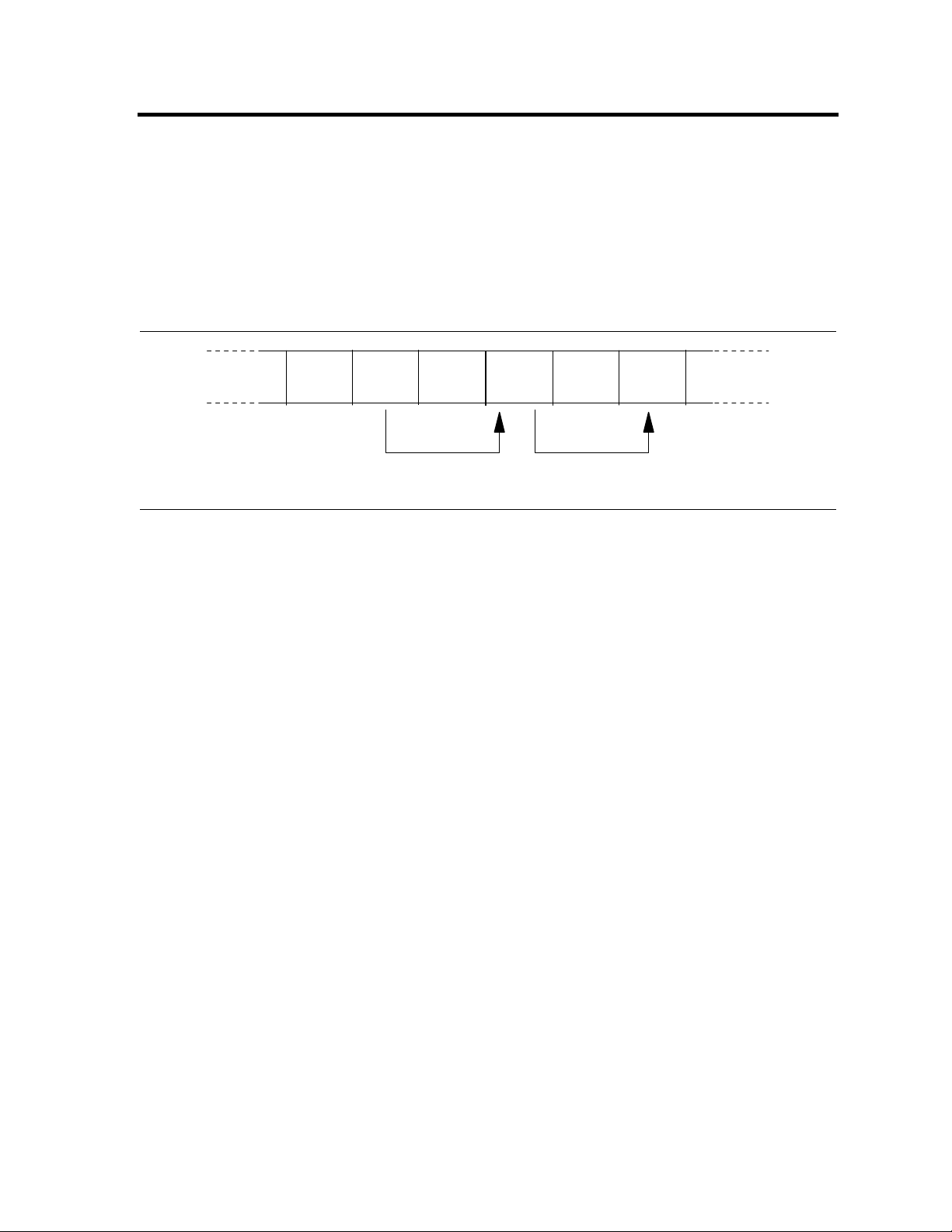
5.0 Defect flagging strategy
Media defects are remapped to the next available sector during the Format Process in manufacturing. The
mapping from LBA to the physical locations is calculated by an internally maintained table.
Shipped format
• Data areas are optimally used.
• No extra sector is wasted as a spare throughout user data areas.
• All pushes generated by defects are absorbed by the spare tracks of the inner zone.
NN+1 N+2 N+3
Figure 1 PList physical format
Defects are skipped without any constraint, such as track or cylinder boundary. The calculation
from LBA to physical is done automatically by internal table. Specification
defect defect
skip
skip
HITACHI Deskstar & CinemaStar P7K500 Hard Disk Drive specification (Rev 1.1)
14
Page 23
5.1 Electrical interface
5.1.1 Connector location
Refer to the following illustration to see the location of the connectors.
PATA MODEL
SATA MODEL
Figure 2 Connector location (PATA)
Figure 3 Connector location (SATA)
HITACHI Deskstar & CinemaStar P7K500 Hard Disk Drive specification (Rev 1.1)
15
Page 24

5.1.1.1 4pin DC power connector (only for PATA)
The DC power connector is designed to mate with AMP part number 1-480424-0 using AMP pins part
number 350078-4 (strip), part number 61173-4 (loose piece), or their equivalents. Pin assignments are
shown in the figure below.
Pin Voltage
4 3 2 1
Figure 4 Power connector pin assignments
1+12 V
2GND
3GND
4+5V
5.1.1.2
The AT signal connector is a 40-pin connector.
The SATA signal connector is a 8-pin connector. Power connector is a 15-pin connector. (SATA Model)
signal connector
HITACHI Deskstar & CinemaStar P7K500 Hard Disk Drive specification (Rev 1.1)
16
Page 25
5.1.2 Signal definition(PATA model)
The pin assignments of interface signals are listed in the figure below:
PIN SIGNAL I/O Type PIN SIGNAL I/O Type
01 RESET- I TTL 02 GND
03 DD7 I/O 3-state 04 DD8 I/O 3-state
05 DD6 I/O 3-state 06 DD9 I/O 3-state
07 DD5 I/O 3-state 08 DD10 I/O 3-state
09 DD4 I/O 3-state 10 DD11 I/O 3-state
11 DD3 I/O 3-state 12 DD12 I/O 3-state
13 DD2 I/O 3-state 14 DD13 I/O 3-state
15 DD1 I/O 3-state 16 DD14 I/O 3-state
17 DD0 I/O 3-state 18 DD15 I/O 3-state
19 GND
21 DMARQ O 3-state 22 GND
23 DIOW-(*) I TTL 24 GND
25 DIOR-(*) I TTL 26 GND
27 IORDY(*) O 3-state 28 CSEL I TTL
29 DMACK- I TTL 30 GND
31 INTRQ O 3-state 32 I
33 DA1 I TTL 34 PDIAG- I/O OC
35 DA0 I TTL 36 DA2 I TTL
37 CSO- I TTL 38 CS1- I TTL
39 DASP- I/O OC 40 GND
(20) key
Table 11 Table of signals
Notes:
1. "O" designat e s an ou t p u t f rom t h e dri ve.
2. "I" designates an input to the drive.
3. "I/O" designates an input/output common.
4. "OC" designates open-collector or open-drain output.
5. The signal lines marked with (*) are redefined during the Ultra DMA protocol to provide special
functions. These lines change from the conventional to special definitions at the moment the Host
decides to allow a DMA burst if the Ultra DMA transfer mode was previously chosen via SetFeatures.
The Drive becomes aware of this change upon assertion of the DMACK- line. These lines revert back
to their original definitions upon the deassertion of DMACK- at the termination of the DMA burst.
Write Operation
Read Operation
Special Definition
(for Ultra DMA)
DDMARDY-
HSTROBE
STOP
HDMARDY-
DSTROBE
STOP
Conventional Definit i on
IORDY
DIOR-
DIOW-
DIORIORDY
DIOW-
Table 12 Signal special definitions for Ultra DMA
HITACHI Deskstar & CinemaStar P7K500 Hard Disk Drive specification (Rev 1.1)
17
Page 26

DD0-DD15 16-bit bi-directional data bus between the host and the drive. The lower 8 lines, DD00-07,
are used for Register and ECC access. All 16 lines, DD00-15, are used for data transfer.
These are 3-State lines with 24 mA current sink capability.
DA0-DA2 Address used to select the individu al register in the drive.
CS0- Chip select signal generated from the Host address bus. When active, one of the Command
Block Registers (Data, Error {Features when written}, Sector Count, Sector Number,
Cylinder Low, Cylinder High, Drive/Head and Status {Command when written} register) can
be selected. (See Table 26: "I/O address map" on page 34)
CS1- Chip select signal generated from the Host address bus. When active one of the Control
Block Registers (Alternate Status {Device Control when written}) can be selected. (See
Table 26: "I/O address map" on page 34)
RESET- This line is used to reset the drive. It shall be kept in Low logic state during power up and in
High thereafter.
DIOW- Its rising edge holds data from the host data bus to a register or data register of the drive.
DIOR- When low, this signal enables data from a register or data register of the drive o nto data bus.
The data on the bus shall be latched on the rising edge of DIOR-.
INTRQ Interrupt is enabled only when the drive is selected and the host activates the nIEN bit in the
Device Control Reg. Otherwise, this signal is in high impedance state regardless of the state
of the IRQ bit. The interrupt is set when the IRQ bit is set by the drive CPU. IRQ is reset to
zero by a host read of the status register or a write to the Command Reg. This signal is a
3-State line with 24 mA sink capability.
DASP- This is a time-multiplexed signal which indicates that a drive is active, or that device 1 is
present. This signal is driven by Open-Drain driver and internally pulled up to 5 volts through
a 10kΩ resistor.
During Power-On initialization or after RESET- is negated, DASP- shall be asserted by
Device 1 within 400 ms to indicate that device 1 is present. Device 0 shall allow up to 450
ms for device 1 to assert DASP-. If device 1 is not present, device 0 may assert DASP- to
drive a LED indica t or.
DASP- shall be negated following acceptance of the first valid command by device 1. At
anytime after negation of DASP-, eithe r drive may assert DASP- to in dicate that a drive is
active.
PDIAG- PDIAG- shall be asserted by device 1 to indicate to device 0 that it has completed
diagnostics. This line is pulled-up to 5 vo lts in the dri ve through a 10k Ω resistor.
Following a Power On Reset, software reset, or RESET-, drive 1 shall negate PDIAG- within
1 ms (to indicate to device 0 that it is busy). Drive 1 shall then assert PDIAG- within 30
seconds to indicate that it is no longer busy and is able to provide stat us.
Following the receipt of a valid Execute Drive Diagnostics command, device 1 shall negate
PDIAG- within 1 ms to indicate to device 0 that it is busy and has not yet passed its drive
diagnostics. If device 1 is present, device 0 shall wait up to 6 seconds from the receipt of a
valid Execute Drive Diagnostics command for drive 1 to assert PDIAG-. Device 1 should
clear BSY before asserting PDIAG-, as PDIAG- is used to indicate tha t device 1 has pa ssed
its diagnos tics and is ready to post status.
If device 1 did not assert DASP- during reset initialization, device 0 shall post its own status
immediatel y after it completes dia gnostics an d clear the device 1 Stat us register to 00h.
Device 0 may be unable to accept commands until it has finished its reset procedure and is
ready (DRDY=1).
Device 1 shall release PDIAG-/CBLID- no later than after the first command following a
power on or hardware reset se q ue nce so th at th e ho st ma y sa mple PDI AG-/CBLID- in order
to detect the presence or absence of an 80-conductor cable assembly.
HITACHI Deskstar & CinemaStar P7K500 Hard Disk Drive specification (Rev 1.1)
18
Page 27

CSEL (Cable Select) (Optional)
The drive is configured as either Device 0 or 1 depending upon the value of CSEL.
• If CSEL is grounded, the device address is 0.
• If CSEL is open , the device address is 1.
KEY Pin position 20 has no connection pin. It is recommended to close the respective position of
the cable connector in order to avoid incorrect insertion by mistake.
IORDY This signal is negated to extend the host transfer cycle when a drive is not ready to respond
to a data transfer request and may be negated when the host transfer cycle is less than 240
ns for PIO data transfer. This signal is an open-drain output with 24 mA sink capability and
an external resistor is needed to pull up this line to 5 volts.
DMACK- This signal shall be used by the host in response to DMARQ to either acknowledge that data
has been accepted or that data is available.
This signal is internally pulled up to 3.3 V through a 15 KΩ resistor. The t ole r a n ce of the
resistor value is –50% to +100%.
DMARQ This signal, used for DMA data transfers between host and drive, shall be asserted by the
drive when it is ready to transfer data to or from the host. The direction of data transfer is
controlled by DIOR- and DIOW-. This signal is used on a handshake manner with DMACK-.
This signal is a 3-state line with 24mA sink capability and internally pulled down to GND
through 10 KΩ resistor.
HDMARDY- (Ultra DMA)
This signal is used only for Ultra DMA data transfers between the host and the device.
HDMARDY- is a flow control signal for Ultra DMA data in bursts. This signal is held asserted
by the host to indicate to the device that the host is ready to receive Ultra DMA data in
transfers. The host may negate HDMARDY- to pause an Ultra DMA data in transfer.
HSTROBE (Ultra DMA)
This signal is used only for Ultra DMA data transfers between the host and the device.
HSTROBE is the data out strobe signal from the host for an Ultra DMA data out transfer.
Both the rising and falling edge of HSTROBE latch the data from DD(15:0) into the device.
The host may stop toggling HSTROBE to pause an Ultra DMA data out transfer.
STOP (Ultra DMA)
This signal is used only for Ultra DMA data transfers between the host and the device.
STOP shall be asserted by the host prior to initiati on of an Ultra DMA burst. STOP shall be
negated by the host before data is transferred in an Ultra DMA burst. Assertion of STOP by
the host during or after data transfer in an Ultra DMA mode signals the termination of the
burst.
DDMARDY- (Ultra DMA)
This signal is used only for Ultra DMA data transfers between the host and the device.
DDMARDY- is a flow control signal for Ultra DMA data out bursts. This signal is held
asserted by the device to indicate to the host that the device is ready to receive Ultra DMA
data out transfers. The device may negate DDMARDY- to pause an Ultra DMA data out
transfer.
DSTROBE (Ultra DMA)
This signal is used only for Ultra DMA data transfers between the host and the device.
DSTROBE is the data in strobe signal from the device for an Ultra DMA data in transfer.
Both the rising and falling edge of DSTROBE latch the data from DD(15:0) into the host. The
device may stop toggling DSTROBE to pause an Ultra DMA data in transfer.
Device Termination
The termination resistors on the device side are implemented on the drive side as follows:
• 33 Ω for DD0 thru DD15, DMARQ, INTRQ
• 82 Ω for CS0-, CS1-, DA0, DA1, DA2, DIOR-, DIOW-, DMACK-
• 22 Ω for IORDY
HITACHI Deskstar & CinemaStar P7K500 Hard Disk Drive specification (Rev 1.1)
19
Page 28
5.1.3 Interface logic signal levels(PATA model)
The interface logic signal has the following electrical specifications:
Inputs Input High Voltage 2.0 V min.
Outputs
Input Low Vol t ag e 0.8 V max.
Output High Voltage 2.4 V min.
Output Low Voltage 0.5 V max.
5.1.4 Signal definition(SATA model)
SATA has receivers and drivers to be connected to Tx+/- and Rx +/- Serial data signal defines the
signal names of I/O connector pin and signal name.
Signal S4 Gnd 2nd mate Gnd
Power P9 V5 5V power 5V
Table 13 Interface connector pins and I/O signals
No.
S1 GND 2nd mate Gnd
S2 A+ Differential signal A from Phy RX+ Input
S3 A-
S5 B- Differential signal B from Phy TX- Output
S6 B+
S7 Gnd 2nd mate Gnd
Key and spacing separate signal and power segments
P1 V33 3.3V power 3.3V
P2 V33 3.3V power 3.3V
P3 V33 3.3V power, pre-charge, 2nd Mate 3.3V
P4 Gnd 1st mate Gnd
P5 Gnd 2nd mate Gnd
P6 Gnd 2nd mate Gnd
P7 V5 5V power,pre-charge,2nd Mate 5V
P8 V5 5V power 5V
P10 Gnd 2nd mate Gnd
P11 Reserved Support s taggered spin -up and LED activity Reserve
P12 Gnd 1st mate Gnd
P13 V12 12V power,pre-chage,2nd mate V12
P14 V12 12V power V12
P15 V12 12V power V12
Plug Connector pin definition Signal I/O
RX- Input
TX+ Output
5.1.4.1 TX+ / TX-
These signals are the outbound high-speed differential signals that are connected to the serial ATA cable
5.1.4.2 RX+ / RX-
These signals are the inbound high-speed differential signals that are connected to the serial ATA cable.
The following standard shall be referenced about signal specifications.
Serial ATA: High Speed Serialized AT Attachment Revision 1.0a 7-January -2003
HITACHI Deskstar & CinemaStar P7K500 Hard Disk Drive specification (Rev 1.1)
20
Page 29
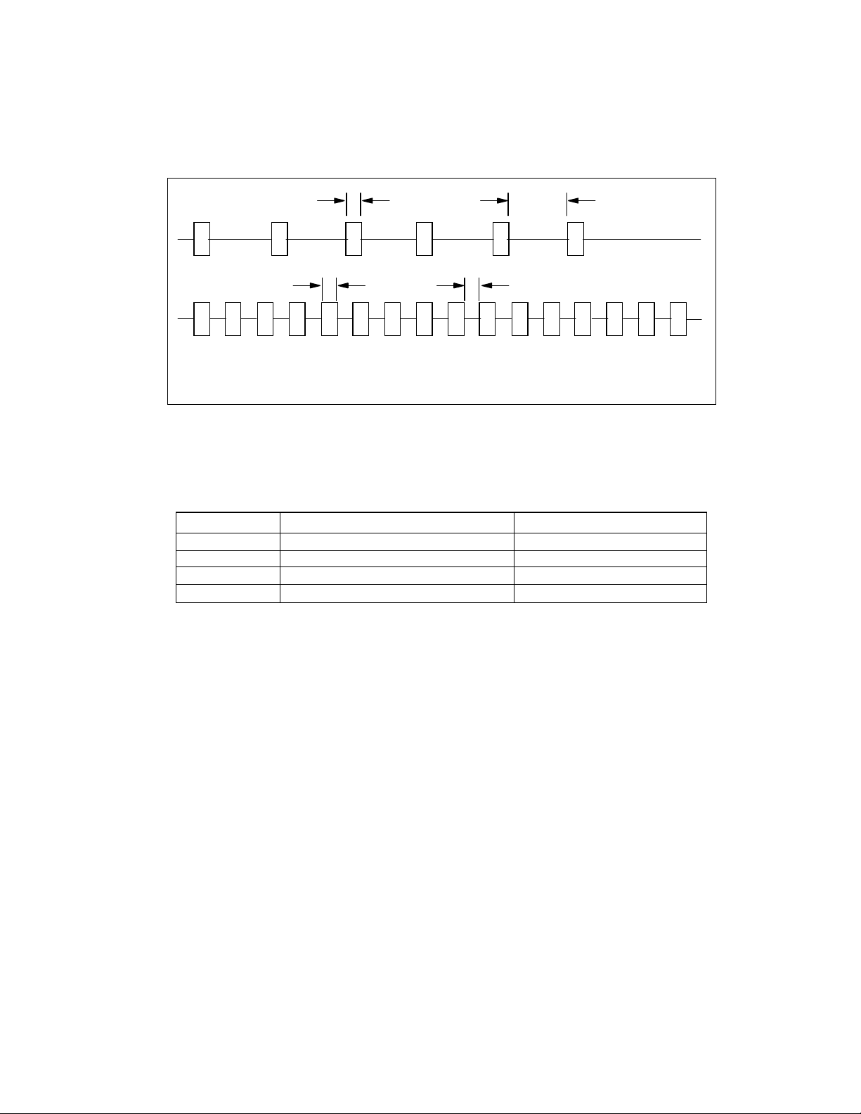
5.1.5 Out of band signaling(SATA model)
Table 14 Parameter descriptions
Figure 5 shows the timing of COMRESET, COMINIT and COMWAKE.
CO M RESET/CO M INIT
COMWAKE
Figure 5 the timing of COMRESET, COMINIT and COMWAK E
t1 ALIGN primitives 106.7
t2 Spacing 320
t3 ALIGN primitives 106.7
t4 Psacing 106.7
t1
t3
PARAMETER DESCRIPTION Nominal (ns)
t2
t4
HITACHI Deskstar & CinemaStar P7K500 Hard Disk Drive specification (Rev 1.1)
21
Page 30
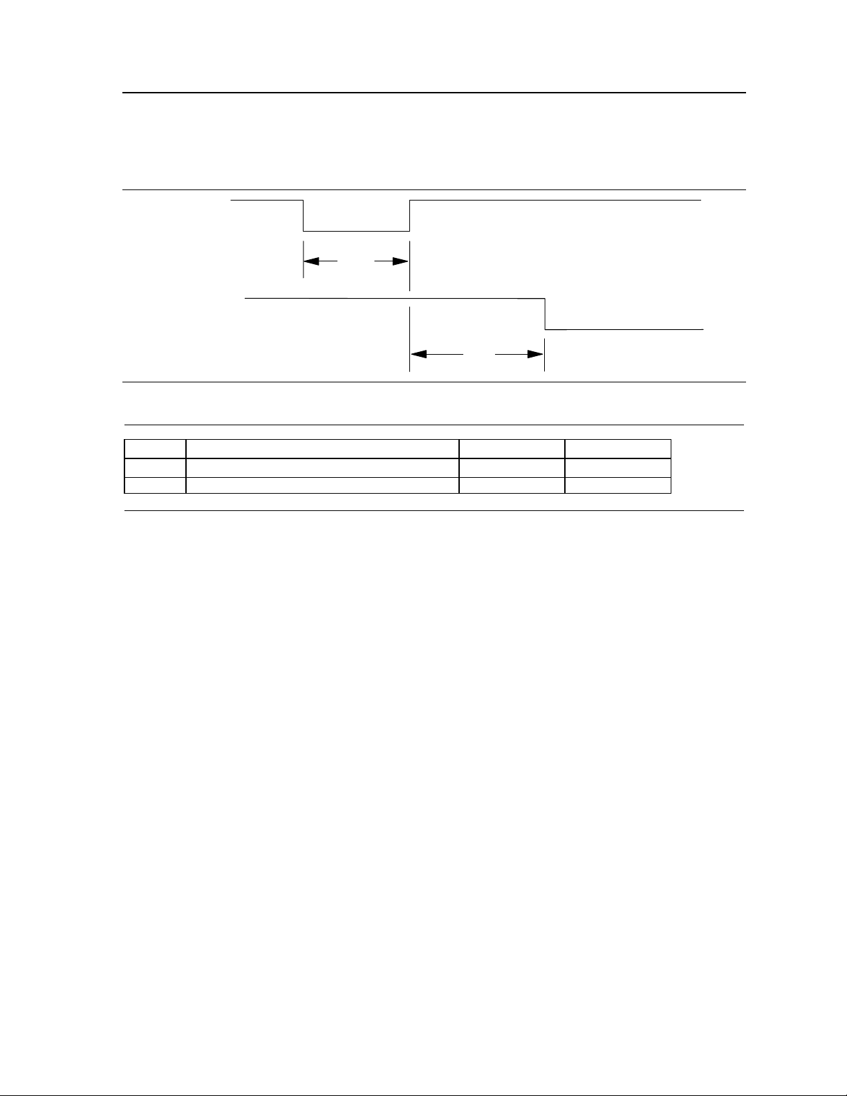
5.2 Signal timings
5.2.1 Reset timings
Drive reset timing.
RESET-
BUSY
t10
t14
Figure 6 System reset timing chart
t10 RESET low width 25
t14 RESET high to not BUSY – 31
Table 15 System reset timing
PARAMETER DESCRIPTION Min (usec) Max (sec )
HITACHI Deskstar & CinemaStar P7K500 Hard Disk Drive specification (Rev 1.1)
22
Page 31

5.2.2 PIO timings
The PIO cycle timings meet Mode 4 of the ATA/ATAPI-6 description.
CS(1:0)
DA(2:0)
t9
DIOR-,
DIOW-
Write data
DD(15:0)
Read data
DD(15:0)
IORDY
t1
t1
t2 t2i
t3 t4
t5 t6
tA
Figure 7 PIO cycle timings chart
tB
t0
(*) Up to ATA-2 (mode-0,1,2)
PARAMETER DESCRIPTION MIN (ns) MAX (ns)
t0 Cycle time 120 –
t1 Address valid to DIOR-/DIOW– setup 25 –
t2 DIOR–/DIOW– pulse width 70 –
t2i DIOR–/DIOW– recovery time 25 –
t3 DIOW– data setup 20 –
t4 DIOW– data hold 10 –
t5 DIOR– data setup 20 –
t6 DIOR– data hold 5 –
t9 DIOR–/DIOW– to address valid hold 10 tA IORDY set up time – 35
tB IORDY pulse width – 1250
Table 16 PIO cycle timings
HITACHI Deskstar & CinemaStar P7K500 Hard Disk Drive specification (Rev 1.1)
23
Page 32

5.2.2.1 Write DRQ interval time
For write sectors and write multiple operations 3.8 μs is inserted from the end of negation of the DRQ bit until
setting of the next DRQ bit.
5.2.2.2 Read DRQ interval time
For read sectors and read multiple operations the interval from the end of negation of the DRQ bit until
setting of the next DRQ bit is as follows:
In the event that a host reads the status register only before the sector or block transfer DRQ
interval, the DRQ interval 4.2 μs
In the event that a host reads the status register after or both before and after the sector or block
transfer, the DRQ interval is 11.5 μs
HITACHI Deskstar & CinemaStar P7K500 Hard Disk Drive specification (Rev 1.1)
24
Page 33

5.2.3 Multiword DMA timings
The Multiword DMA timing meets Mode 2 of the ATA/ATAPI-6 description.
CS0-/CS1-
DMARQ
DMACK-
DIOR-/DIOW-
READ DATA
WRITE DATA
tM
tLR/tLW
t0
tI tD
tE
tG
Figure 8 Multiword DMA cycle timing chart
tFtG
tH
tKR/tKW
tN
tJ
tZ
t0 Cycle time 120 –
tD DI O R –/DIOW– asserted pulse width 70 –
tE DIOR– data access – 50
tF DIOR– data hold 5 –
tG DIOR–/DIOW– data set u p 20 –
tH DIOW– data hold 10 –
tI DMACK– to –DIOR–/DIOW– setup 0 –
tJ DIOR–/DIOW– to DMACK– ho l d 5 –
tKR/tKW DIOR–/DIOW– negat ed p ul se width 25 –
tLR/tLW DIOR–/DIOW – t o DM ARQ– delay – 35
tM CS (1:0) valid to DIOR–/DIOW– 25 –
tN CS (1:0) hold 10 –
tZ DMACK– to read data released – 25
Table 17 Multiword DMA cycle timings
PARAMETER DESCRIPTION MIN (ns) MAX (ns)
HITACHI Deskstar & CinemaStar P7K500 Hard Disk Drive specification (Rev 1.1)
25
Page 34

5.2.4 Ultra DMA timings
The Ultra DMA timing meets Mode 0,1,2,3 4, and 5 of the Ultra DMA Protocol.
5.2.4.1 Initiating Read DMA
DMARQ
tUI
DMACK-
tACK
tENV
STOP
tACK
tENV
HDMARDY-
tZIORDY
DSTROBE
tAZ
DD(15:00)
xxxxxxxxxxxxxxxxxxxxxxxxx
xxx xxx xxx
Host drives DD
Figure 9 Ultra DMA cycle timing chart (Initiating Read)
tUI
tACK
tENV
tZIORDY
tFS
tCYC
t2CYC
tAZ
tZAD
tDS
tDH
tDZFS
Table 18 Ultra DMA cycle timings (Initiating Read)
PARAMETER
DESCRIPTION
(all values in ns)
Unlimited interlock time
Setup time before
–DMACK
Envelope time
Minimum time before
driving IORDY
First DSTROBE time
Cycle time
Two cycle time
Maximum time allowed for
output drivers to release
Maximum time allowed for
output drivers to assert
Data setup time (at host)
Data hold time (at host )
Time from data output
released-to-driving u nt il
the first transition of c rit ical
timing
MODE0
MIN MAX MIN MAX MIN MAX MIN MAX MIN MAX MIN MAX MIN MAX
0 – 0 – 0 0 0 – 0 – 0 – 0 –
20 – 20 – 20 – 20 – 20 – 20 – 20 –
20 70 20 70 20 70 20 55 20 55 20 50 20 50
0 – 0 – 0 – 0 – 0 – 0 – 0 –
0 230 0 200 0 170 0 130 0 120 0 90 0 80
112 – 73 – 54 – 39 – 25 – 17 – 13 –
230 – 153 – 115 – 86 – 57 – 38 –
– 10 – 10 – 10 – 10 – 10 – 10 – 10
0 – 0 – 0 – 0 – 0 – 0 – 0 –
15 – 10 – 7 – 7 – 5 – 4 – 2.6 –
5 – 5 – 5 – 5 – 5 – 4.6 – 3.5 –
70 - 48 - 31 - 20 - 6.7 - 25 - 17.5 -
MODE1 MODE2 MODE3 MODE4 MODE5 MODE6
tFS
tDZFS
tZAD
RD Data
t2CYC
tCYC tCYC
tDS
tDH
RD Data
Device drives DD
tDS
tDH
RD Data
29
–
HITACHI Deskstar & CinemaStar P7K500 Hard Disk Drive specification (Rev 1.1)
26
Page 35

5.2.4.2 Host Pausing Read DMA
DMARQ
DMACK-
tRP
STOP
HDMARDY-
tRFS
DSTROBE
Figure 10 Ultra DMA cycle timing chart (Host pausing Read)
MODE1 MODE2 MODE3 MODE4 MODE5 MODE6
PARAMETER DESCRIPTION
tRP
tRFS
(all values in ns)
Ready to pause time
HDMARDY– to final DSTROBE
time
MODE0
MIN MAX MIN MAX MIN MAX MIN MAX MIN MAX MIN MAX MIN MAX
160 – 125 – 100 – 100 – 100 – 85 – 85 –
– 75 – 70 – 60 – 60 – 60 – 50
Table 19 Ultra DMA cycle timings (Host pausing Read)
50
HITACHI Deskstar & CinemaStar P7K500 Hard Disk Drive specification (Rev 1.1)
27
Page 36

5.2.4.3 Host Terminating Read DMA
DMARQ
DMACK-
STOP
HDMARDY-
DSTROBE
DD(15:00)
tLI
tMLI
tRP
tRFS
tLI
tAZ
xxx
RD Data
xxxxxxxxxxxxxxxxxx
tZAH
Device drives DD
Figure 11 Ultra DMA cycle timing chart (Host terminating Read)
xxx
CRC
Host drives DD
tACK
tACK
tIORDYZ
tCHtCS
xxxxxxxxxx
MODE1 MODE2 MODE3 MODE4 MODE5 MODE6
MODE0
MIN MAX MIN MAX MIN MAX MIN MAX MIN MAX MIN MAX MIN MAX
– 75 – 70 – 60 – 60 – 60 – 50 – 50
160 – 125 – 100 – 100 – 100 – 85 – 85 –
0 150 0 150 0 150 0 100 0 100 0 75 0 60
– 10 – 10 – 10 – 10 – 10 – 10 – 10
20 – 20 – 20 – 20 – 20 – 20 – 20 –
20 – 20 – 20 – 20 – 20 – 20 – 20 –
15 – 10 – 7 – 7 – 5 – 5 – 5 –
5 – 5 – 5 – 5 – 5 – 5 – 5 –
20 – 20 – 20 – 20 – 20 – 20 – 20 –
– 20 – 20 – 20 – 20 – 20 – 20 – 20
tRFS
tRP
tLI
tAZ
tZAH
tMLI
tCS
tCH
tACK
tIORDYZ
PARAMETER
DESCRIPTION
(all values in ns)
HDMARDY– to final
DSTROBE time
Ready to pause time
Limited interlock time
Maximum time allowed for
output drivers to release
Minimum delay time
required for output
Interlocking time with
minimum
CRC word setup time (at
device side)
CRC word hold time (at
device side)
Hold time for DMACK –
Maximum time before
releasing IORDY
Table 20 Ultra DMA cycle timings (Host terminating Read)
HITACHI Deskstar & CinemaStar P7K500 Hard Disk Drive specification (Rev 1.1)
28
Page 37

5.2.4.4 Device Terminating Read DMA
DMARQ
DMACK-
STOP
HDMARDY-
DSTROBE
DD(15:00)
Time from DSTROBE
tSS
tLI
tAZ
tZAH
tMLI
tCS
tCH
tACK
tIORDYZ
edge to negation of
DMARQ
Limited interlock time
Maximum time allowed
for output drivers to
release
Minimum delay time
required for output
Interlock time with
minimum
CRC word setup ti me
(at device side)
CRC word hold time (at
device side)
Hold time after
DMACK–
Maximum time before
releasing IORDY
Device drives DD
Figure 12 Ultra DMA cycle timing chart (Device terminating Read)
PARAMETER
DESCRIPTION
(all values in ns)
tSS
tAZ
xxxxx
tLI
tLI
tLI
xxxxxxxxxxxxxxxxxx
tMLI
tIORDYZ
CRC
tACK
tACK
tCHtCS
xxxxxxxxxx
tZAH
Host drives DD
MODE1 MODE2 MODE3 MODE4 MODE5 MODE6
MODE0
MIN MAX MIN MAX MIN MAX MIN MAX MIN MAX MIN MAX MIN MAX
50 – 50 – 50 – 50 – 50 – 50 – 50 –
0 150 0 150 0 150 0 100 0 100 0 75 0 60
– 10 – 10 – 10 – 10 – 10 – 10 – 10
20 – 20 – 20 – 20 – 20 – 20 – 20 –
20 – 20 – 20 – 20 – 20 – 20 – 20 –
15 – 10 – 7 – 7 – 5 – 5 – 5 –
5 – 5 – 5 – 5 – 5 – 5 – 5 –
20 – 20 – 20 – 20 – 20 – 20 – 20 –
– 20 – 20 – 20 – 20 – 20 – 20 – 20
Table 21 Ultra DMA cycle timings (Device Terminating Read)
HITACHI Deskstar & CinemaStar P7K500 Hard Disk Drive specification (Rev 1.1)
29
Page 38

5.2.4.5 Initiating Write DMA
DMARQ
tUI
DMACK-
STOP
DDMARDY-
HSTROBE
DD(15:0)
tUI
tACK
tENV
tZIORDY
tLI
tCYC
t2CYC
tDS
tDH
Unlimited interlock time
Setup time before
DMACK–
Envelope time
Minimum time before
driving IORDY
Limited interlock time
Cycle time
Two Cycle time
Data setup time (at
device side)
Data hold time (at
device side)
tACK
tENV
tZIORDY tLI
tACK
xxxxxxxxxxxxxxxxxxxxxxxxxxxxxxx
Figure 13 Ultra DMA cycle timing chart (Initiating Write)
PARAMETER
DESCRIPTION
(all values in ns)
MIN MAX MIN MAX MIN MAX MIN MAX MIN MAX MIN MAX MIN MAX
20 – 20 – 20 – 20 – 20 – 20 – 20 –
20 70 20 70 20 70 20 55 20 55 20 50 20 50
112 – 73 – 54 – 39 – 25 – 16.8 – 13.0 –
230 – 154 – 115 – 86 – 57 – 38 – 29 –
15 – 10 – 7 – 7 – 5 – 4 – 2.6 –
MODE1 MODE2 MODE3 MODE4 MODE5 MODE6
MODE0
0 – 0 – 0 – 0 – 0 – 0 – 0 –
0 – 0 – 0 – 0 – 0 – 0 – 0 –
0 150 0 150 0 150 0 100 0 100 0 75 0 60
5 – 5 – 5 – 5 – 5 – 4.6 – 3.5 –
tUI
WT Data
Host drives DD
t2CYC
tCYC tCYC
tDH
tDS
xxx
WT Data
xxx
tDS
tDH
WT Data
Table 22 Ultra DMA cycle timings (Initiating Write)
HITACHI Deskstar & CinemaStar P7K500 Hard Disk Drive specification (Rev 1.1)
30
Page 39

5.2.4.6 Device Pausing Write DMA
DMARQ
tRP
DMACKSTOP
DDMARDY-
tRFS
DSTROBE
Figure 14 Ultra DMA cycle timing chart (Device Pausing Write)
tRP
tRFS
PARAMETER
DESCRIPTION
(all values in ns)
Ready to pause time
DDMARDY– to final
HSTROBE time
MODE0
MIN MAX MIN MAX MIN MAX MIN MAX MIN MAX MIN MAX MIN MAX
160 – 125 – 100 – 100 – 100
– 75 – 70 – 60 – 60 – 60 – 50 – 50
MODE1 MODE2 MODE3 MODE4 MODE5
Table 23 Ultra DMA cycle timings (Device Pausing Write)
-
85 – 85 –
MODE6
HITACHI Deskstar & CinemaStar P7K500 Hard Disk Drive specification (Rev 1.1)
31
Page 40

(
5.2.4.7 Device Terminating Write DMA
DMARQ
tRP
tLI
DMACK-
STOP
DDMARDY-
tRFS
tLI
HSTROBE
DD(15:00)
xxx
WT Data
xxxxxxxxxxxxxxxxxxxxxxxxxx
Host drives DD
Figure 15 Ultra DMA cycle timing char t (Device Terminating Write)
PARAMETER
tRFS
tRP
tLI
tMLI
tCS
tCH
tACK
tIORDYZ
DESCRIPTION
all values in ns)
DDMARDY to final
HSTROBE time
Ready to pause
time
Limited interlock
time
Interlock time with
minimum
CRC word setup
time (at device
side)
CRC word hold
time (at device
side)
Hold time for
–DMACK
Maximum time
before releasing
IORDY
Table 24 Ultra DMA cycle timings (Device terminating Write)
MODE0 MODE1 MODE2 MODE3 MODE4 MODE5 MODE6
MIN MAX MIN MAX MIN MAX MIN MAX MIN MAX MIN MAX MIN MAX
– 75 – 70 – 60 – 60 – 60 – 50 – 50
160 – 125 – 100 – 100 – 100 – 85 – 85 –
0 150 0 150 0 150 0 100 0 100 0 75 0
20 – 20 – 20 – 20 – 20 – 20 – 20 –
15 – 10 – 7 – 7 – 5 – 5 – 5 –
5 – 5 – 5 – 5 – 5 – 5 – 5 –
20 – 20 – 20 – 20 – 20 – 20 – 20 –
– 20 – 20 – 20 – 20 – 20 – 20 – 20
tMLI
tIORDYZ
CRC
tACK
tACK
tCHtCS
xxxxxxxxxx
60
HITACHI Deskstar & CinemaStar P7K500 Hard Disk Drive specification (Rev 1.1)
32
Page 41

(
)
5.2.4.8 Host Terminating Write DMA
DMARQ
tLI
DMACK-
tSS
STOP
tLI
DDMARDY-
tLI
HSTROBE
DD(15:00)
xxxxxxxxxxxxxxxxxxxxxxxxxxxxxxxxxxxxx
Host drives DD
Figure 16 Ultra DMA cycle timing chart (Host Terminating Write)
PARAMETER
tSS
tLI
tMLI
tCS
tCH
tACK
tIORDYZ
DESCRIPTION
all values in ns
Time from
HSTROBE to
edge assertion of
STOP
Limited interlock
time
Interlock time with
minimum
CRC word setup
time (at device
side)
CRC word hold
time (at device
side)
Hold time for
DMACK–
Maximum time
before releasing
IORDY
Table 25 Ultra DMA cycle timings (Host Terminating Write)
MODE0
MIN MAX MIN MAX MIN MAX MIN MAX MIN MAX MIN MAX MIN MAX
50 – 50 – 50 – 50 – 50 – 50 – 50 –
0 150 0 150 0 150 0 100 0 100 0 75 0
20 – 20 – 20 – 20 – 20 – 20 – 20 –
15 – 10 – 7 – 7 – 5 – 5 – 5 –
5 – 5 – 5 – 5 – 5 – 5 – 5 –
20 – 20 – 20 – 20 – 20 – 20 – 20 –
– 20 – 20 – 20 – 20 – 20 – 20 – 20
MODE1 MODE2 MODE3 MODE4 MODE5 MODE6
tMLI
tIORDYZ
CRC
tACK
tACK
tCHtCS
xxxxxxxxxx
60
HITACHI Deskstar & CinemaStar P7K500 Hard Disk Drive specification (Rev 1.1)
33
Page 42

5.2.5 Addressing of registers
The host addresses the drive through a set of registers called the Task File. These registers are mapped into
the I/ O space of the host. Two chip select lines (CS0– and CS1–) and three address lines (DA0-02) are
used to select one of these registers, while a DIOR– or DIOW– is provided at the specified time.
The CS0– is used to address Command Block registers. while the CS1– is used to address Control Block
registers.
The following table shows the I/ O address map.
CS0– CS1– DA2 DA1 DA0 DIOR– = 0 (Read) DIOW– = 0 (Write)
0 1 0 0 0 Data Reg. Data Reg.
0 1 0 0 1 Error Reg. Features Reg.
0 1 0 1 0 Sector count Reg. Sector count Reg.
0 1 0 1 1 Sector number Reg. Sector number Reg.
0 1 1 0 0 Cylinder low Reg. Cylinder low Reg.
0 1 1 0 1 Cylinder high Reg. Cylinder high Reg.
0 1 1 1 0 Device/Head Reg. Device/Head Reg.
0 1 1 1 1 Status Re g . Command Reg.
Command Block Registers
1 0 1 1 0 Alt. Status Reg. Device control Reg.
Control Block Registers
Table 26 I/O address map
Note: "Addr" field is shown as an example.
During DMA operation (from writing to the command register until an interrupt) not all registers are
accessible. For example, the host is not supposed to read status register contents before interrupt (the
value is invalid).
5.2.6 Cabling
The maximum cable length from the host system to the drive plus circuit pattern length in the host system
shall not exceed 18 inches.
For higher data transfer application (>8.3 MB/s) a modification in the system design is recommended to
reduce cable noise and cross-talk, such as a shorter cable, bus termination, or a shielded cable.
For systems operating with Ultra DMA mode 3, 4, and 5, 80-conductor ATA cable assembly shall be used.
HITACHI Deskstar & CinemaStar P7K500 Hard Disk Drive specification (Rev 1.1)
34
Page 43

5.3 Jumper settings(PATA model)
5.3.1 Jumper pin location
Figure 17 Jumper pin location
Jumper pins
5.3.2 Jumper pin identification
Figure 18 Jumper pin identification
Pin I
Pin A
Pin B
DERA001.prz
HITACHI Deskstar & CinemaStar P7K500 Hard Disk Drive specification (Rev 1.1)
35
Page 44

5.3.3 Jumper pin assignment
There are four jumper settings as shown in the following sections:
• 16 logical head default (normal use)
• 15 logical head default
• 32 GB clip
• Power up in standby
Within each of these four jumper settings the pin assignment selects Device 0, Device 1, Cable Selection,
or Device 1 Slave Present as shown in the following figures.
The Device 0 setting automatically recognizes device 1 if it is present.
The Device 1 Slave Present setting is for a slave device that does not comply with the ATA specification.
Note: In conventional terminology "Device 0" designates a Master and "Device 1" designates a Slave.
RSV
IGECA
Figure 49. Jumper pin assignment
GND
H
DS
GND GND RSV
BF
RS V
CS/SP
D
GND
HITACHI Deskstar & CinemaStar P7K500 Hard Disk Drive specification (Rev 1.1)
36
Page 45

5.3.4 Jumper positions
5.3.4.1
The figure below shows the jumper positions used to select Device 0, Device 1, Cable Selection, or Device
1 (Slave) Pres en t .
16 logical head default (normal use)
I
G
ECA
HFDB
I
G
ECA
HFDB
I
G
ECA
HFDB
I
G
ECA
HFDB
I
G
ECA
HFDB
Figure 19 Jumper positions for normal use
DEVICE 0 (Master)
DEVICE 1 (Slave)
CABLE SEL
DEVICE 1 (Slave) Present
Shipping Default Condition
(CABLE SEL)
Notes:
1. To enable the CSEL mode (Cable Selection mode) the jumper block must be installed at E-F. In
the CSEL mode the drive address is determined by AT interface signal #28 CSEL as follows:
When CSEL is gr ounded or at a low level, the drive address is 0 (Devi ce 0).
When CSEL is open or at a high level, the drive address is 1 (Device 1).
2. In CSEL mode, installing or removing the jumper blocks at A-B or C-D position does not affect any
selection of Device or Cable Selection mode.
3. The shipping default position is Cable Select position.
HITACHI Deskstar & CinemaStar P7K500 Hard Disk Drive specification (Rev 1.1)
37
Page 46

5.3.4.2 15 logical head default
The figure below shows the jumper positions used to select Device 0, Device 1, Cable Selection, or Device
1 (Slave) Present setting 15 logical heads instead of default 16 logical head models.
I
G
HFDB
I
G
HFDB
I
G
HFDB
I
G
HFDB
Notes:
1. To enable the CSEL mode (Cable Selection mode) the jumper block must be installed at E-F. In
the CSEL mode, the drive address is determined by AT interface signal #28 CSEL as follows:
When CSEL is gr ounded or at a low level, the drive address is 0 (Devi ce 0).
When CSEL is open or at a high level, the drive address is 1 (Device 1).
2. In CSEL mode, installing or removing the jumper blocks at A-C or B-D position does not affect any
selection of Device or Cable Selection mode.
ECA
DEVICE 0 (Master)
ECA
DEVICE 1 (Slave)
ECA
CABLE SEL
ECA
DEVICE 1 (Slave) Present
Figure 20 Jumper positions for 15 logical head default
HITACHI Deskstar & CinemaStar P7K500 Hard Disk Drive specification (Rev 1.1)
38
Page 47

5.3.4.3 Capacity clip to 32GB
The figure below shows the jumper positions used to select Device 0, Device 1, Cable Selection, or Device
1 (Slave) Present while setting the drive capacity down either to 32GB for the purpose of compatibility.
I
G
HFDB
I
G
HFDB
ECA
ECA
DEVICE 0 (Master)
DEVICE 1 (Slave)
I
G
HFDB
I
G
HFDB
ECA
ECA
CABLE SEL
DEVICE 1 (Slave) Present
Figure 21 Jumper positions for capacity clip to 32GB
Notes:
The jumper setting acts as a 32GB clip which clips the LBA to 66055248. The CHS is unchanged from the
factory default of 16383/16/63.
HITACHI Deskstar & CinemaStar P7K500 Hard Disk Drive specification (Rev 1.1)
39
Page 48

5.3.4.4 Power Up In Standby
The figure below shows the jumper positions used to select Device 0, Device 1, Cable Selection, or Device
1 (Slave) Present to enable Power Up In Standby.
I
G
ECA
HFDB
DEVICE 0 (M aster)
I
G
ECA
DEVICE 1 (Slave)
HFDB
I
G
ECA
CABLE SEL
HFDB
I
G
ECA
DEVICE 1 (Slave) Present
HFDB
Figure 22 Jumper settings for Disabling Auto Spin
Notes:
1. These ju mp er se ttings are us ed for limiting po we r s upp l y current when mu l tiple drives are used.
2. Command to spin up is SET FEATURES (subcommand 07h). Refer to 10.37 Set Feat ures.
3. To enable the CSEL mode (Cable Selection mode) the jumper block must be installed at E-F.
In CSEL mode, the drive address is determined by AT interface signal #28 as follows:
•
When CSEL is grounded or at a low level, the drive address is 0 (Device 0).
•
When C SEL is open or a t a high level, the drive ad dress is 1 (Device 1).
HITACHI Deskstar & CinemaStar P7K500 Hard Disk Drive specification (Rev 1.1)
40
Page 49

5.4 Environment
5.4.1 Temperature and humidity
Operating conditions
Temperature
Relative humidity
Maximum wet bulb temperature
Maximum temperature gradient
Altitude
Non-Op conditions
Temperature
Relative humidity
Maximum wet bulb temperature
Maximum temperature gradient
Altitude
Table 27 Temperature and humidity
Notes:
1. The system is responsible for providing sufficient ventilation to maintain a surface temperature
below 65°C at the center of the top cover of the drive.
2. Non condensing conditions should be maintained at any time.
3. Maximum storage period within shipping package is one year,
0 to 60°C
8 to 90% non-condensing
29.4°C non-condensing
20°C/Hour
–300 to 3,048 m
-40 to 70°C
5 to 95% non-condensing
35°C non-condensing
30°C/Hour
–300 to 12,000 m
HITACHI Deskstar & CinemaStar P7K500 Hard Disk Drive specification (Rev 1.1)
41
Page 50

%
100
90
80
Environment Specification
31C/90%
36C/95%
Wet Bulb 35C
70
60
50
40
30
Relative Humidity (%)
20
10
0
Non-operating Operating
-40 -20 0 20 40 60
Figure 23 Limits of temperature and humidity
Note: Storage temperature range is 0 to 70°C
Wet Bulb 29.4C
70C/11
60C/10%
Temperature (C)
5.4.2 Corrosion test
The drive shows no sign of corrosion inside and outside of the hard disk assembly and is functional after
being subjected to seven days at 50°C with 90% relative humidity.
HITACHI Deskstar & CinemaStar P7K500 Hard Disk Drive specification (Rev 1.1)
42
Page 51

1
5.5 DC power requirements
Damage to the drive electronics may result if the power supply cable is connected or disconnected to the
legacy power connector while power is being applied to the drive (no hot plug/unplug is allowed). If SATA
power supply cable is connected or disconnected to the SATA power connector, hot plug/unplug is allowed.
5.5.1 Input voltage
Input voltage During run and spin up
+5 Volts Supply 5V ± 5% –0.3 to 5.5V 0 to 5sec
+12 Volts Supply 12V ±10% –0.3 to 15.0V 0 to 5sec
Table 28 Input voltage
Caution : To avoid damage to the drive electronics, power supply voltage spikes must not exceed
specifications.
5.5.2 Power supply current (typical)
Absolute max
spike voltage
Supply rise time
Power supply current of
2 Disk PATA models
(values in milliamps. RMS) TPop MeanT Std Dev TPop MeanT Std Dev
TIdle averageT 130 10 320 15
TIdle ripple (peak-to-peak)T 200 10 300 20
Low RPM Idle 80 10 130 15
Low RPM Idle Ripple 100 10 250 20
Unload Idle average 80 10 280 15
Unload Idle Ripple 100 10 300 20
Random R/W averageP
P
Random R/W p eak 700 20 1500 40
TStart up (max)T 400 20 2000 50
TStandby averageT 75 10 5 5 0.5
TSleep averageT 65 10 5 5 0.5
T+5 VoltsT [mA] T+12 VoltsT [mA]
TTotalT
240 10 560 15
T
[W]T
4.5
2.0
3.8
7.9
Table 29 Power supply current of 2 Disk PATA models
Except for a peak of less than 100 μs duration.P
1
Random R/W : 40 IOPS / 16 Blocks Random Write and Random Read
HITACHI Deskstar & CinemaStar P7K500 Hard Disk Drive specification (Rev 1.1)
43
Page 52

Power supply current of
1 Disk PATA models
(values in milliamps. RMS) TPop MeanT Std Dev TPop MeanT Std Dev
TIdle averageT 130 10 220 15
TIdle ripple (peak-to-peak)T 200 10 300 20
Low RPM Idle 80 10 110 15
Low RPM Idle Ripple 100 10 250 20
Unload Idle average 80 10 210 15
Unload Idle Ripple 100 10 300 20
Random R/W average1
Random R/W p eak 700 20 1200 40
TStart up (max)T 400 20 2000 50
TStandby averageT 75 10 5 5 0.5
TSleep averageT 65 10 5 5 0.5
T+5 VoltsT [mA] T+12 VoltsT [mA]
TTotalT
240 10 410 15
T
[W]T
3.3
1.7
2.9
6.1
Table 30 Power supply current of 1 Disk PATA models
Except for a peak of less than 100 μs duration
1
Random R/W : 40 IOPS / 16 Blocks Random Write and Random Read
Power supply current of
2 Disk SATA models
(values in milliamps. RMS)
Idle average 190 10 320 15
Idle ripple (peak-to-peak) 200 10 300 20
Low RPM Idle 140 10 130 15
Low RPM Idle Ripple 100 10 250 20
Unload Idle average 140 10 280 15
Unload Idle Ripple 100 10 300 20
Random R/W average1 300 10 560 15
Random R/W peak 800 20 1500 40
+5 Volts [mA] +12 Volts [mA]
Pop Mean Std Dev Pop Mean Std Dev
Total
[W]
4.8
2.3
4.1
8.2
Start up (max) 500 20 2000 50
Standby average 135 10 5 5 0.8
Sleep average 130 10 5 5 0.8
Table 31 Power supply current of 2 Disk SATA models
Except for a peak of less than 100 μs duration
1
Random R/W : 40 IOPS / 16 Blocks Random Write and Random Read
HITACHI Deskstar & CinemaStar P7K500 Hard Disk Drive specification (Rev 1.1)
44
Page 53

Power supply current of
1 Disk SATA models
(values in milliamps. RMS)
Idle average 190 10 220 15
Idle ripple (peak-to-peak) 200 10 300 20
Low RPM Idle 140 10 110 15
Low RPM Idle Ripple 100 10 250 20
Unload Idle average 140 10 210 15
Unload Idle Ripple 100 10 300 20
Random R/W average1 300 10 410 15
Random R/W peak 800 20 1200 40
Start up (max) 500 20 2000 50
Standby average 135 10 5 5 0.8
Sleep average 130 10 5 5 0.8
+5 Volts [mA] +12 Volts [mA]
Pop Mean Std Dev Pop Mean Std Dev
Total
[W]
3.6
2.0
3.2
6.4
Table 32 Power supply current of 1 Disk SATA models
Except for a peak of less than 100 μs duration
1
Random R/W : 40 IOPS / 16 Blocks Random Write and Random Read
5.5.3 Power supply generated ripple at drive power connector
+5V DC 150 0-10
+12V DC 250 0-10
Maximum (mV pp) MHz
Table 33 Power supply generated ripple at drive power connector
During drive start up and seeking 12-volt ripple is generated by the drive (referred to as dynamic loading). If
the power of several drives is daisy chained together, the power supply ripple plus the dynamic loading of
the other drives must remain within the above regulation tolerance. A common supply with separate power
leads to each drive is a more desirable method of power distribution.
To prevent external electrical noise from interfering with the performance of the drive, the drive must be held
by four screws in a user system frame which has no electrical level difference at the four screws position a nd
has less than ±300 millivolts peak to peak level difference to the ground of the drive power connector.
HITACHI Deskstar & CinemaStar P7K500 Hard Disk Drive specification (Rev 1.1)
45
Page 54

5.6 Reliability
5.6.1 Data integrity
No more than one sector is lost at Power loss condition during the write operation when the write cache
option is disabled. If the write cache option is active, the data in write cache will be lost. To prevent the loss
of customer data, it is recommended that the last write access before power off be issued after setting the
write cache off.
5.6.2 Cable noise interference
To avoid any degradation of performance throughput or error rate when the interface cable is routed on top
or comes in contact with the HDA assembly, the drive must be grounded el ectrically to the system frame by
four screws. The common mode noise or voltage level difference between the system frame and power
cable ground or AT interface cable ground should be in the allowable level specified in the power
requireme nt section.
5.6.3 Start/stop cycles
The drive withstands a minimum of 50,000 start/stop cycles in a 40° C environment and a minimum of
10,000 start/stop cycles in extreme temperature or humidity within the operating range. .
5.6.4 Preventive maintenance
None
5.6.5 Data reliability
Probability of not recovering data is 1 in 10
ECC On The Fly correction
1 Symbol : 10 bits
No Interleave
34 symbol ECC
This implementation always recovers 16 symbol random erros and a 330-bit continuous burst error
14
bits read
5.6.6 Required Power-Off Sequence
The required BIOS sequence for removing power from the drive is as follows:
Step 1: Issue one of the following commands.
Standby
Standby immediate
Sleep
Note: Do not use the Flush Cache command for the power off sequence because this command does
not invoke Unload
Step 2: Wait until the Command Complete status is returned. In a typical case 350 ms are required for
the command to finish completion; however, the BIOS time out value needs to be 30 seconds
considering error recovery time. Refer to section 11.0 "Timings," on page 266.
Step 3: Terminate power to HDD.
HITACHI Deskstar & CinemaStar P7K500 Hard Disk Drive specification (Rev 1.1)
46
Page 55

5.7 Mechanical specifications
5.7.1 Physical dimensions
Figure 24 Top and side views with breather hole location and mechanical dimensions
All dimensions ar e in mi l li m et er s .
HITACHI Deskstar & CinemaStar P7K500 Hard Disk Drive specification (Rev 1.1)
47
Page 56

Figure 25 Bottom and side views with mounting hole locations
All dimensions in the above figure are in millimeters.
The breather hole must be kept uncovered in order to keep the air pressure inside of the disk enclosure
equal to external air pressure.
The following table shows the physical dimensions of the drive.
Height (mm) Width (mm) Length (mm) Weight (gram)
26.1 MAX 101. 6 ± 0.25 147 MAX 550 MAX
Table 34 Physical Dimensions
HITACHI Deskstar & CinemaStar P7K500 Hard Disk Drive specification (Rev 1.1)
48
Page 57

5.7.2 Hole locations
The mounting hole location and size for the hard disk drive is shown below.
(6X) Max. penetration 4.5 mm
(4)
Side View
Bottom View
(3)
(5)(6) (7)
I/F Connector
(4X) Max. penetration 4.0 mm
Thread (1) (2) (3) (4) (5) (6) (7)
6-32UNC 41.28±0.5 44.45±0.2 95.25±0.2 6.35±0.2 28.5±0.5 60.0±0.2 41.6±0.2
Figure 26 Mounting hole locations (all dimensions are in mm)
(1)(2)
HITACHI Deskstar & CinemaStar P7K500 Hard Disk Drive specification (Rev 1.1)
49
Page 58

5.7.3 Connector locations
PATA Model
T
Figure 27 Connector locations
SATA Model
HITACHI Deskstar & CinemaStar P7K500 Hard Disk Drive specification (Rev 1.1)
50
Page 59

5.7.4 Drive mounting
The drive will operate in all axes (6 directions). Performance and error ra te will stay within specification limits
if the drive is operated in the other orientations from which it was formatted.
For reliable operation, the drive must be mounted in the system securely enough to prevent excessive
motion or vibration of the drive during seek operation or spindle rotation, using appropriate screws or
equivalent mounting hardware.
The recommended mounting screw torque is 0.6 – 1.0 Nm (6-10 Kgf.cm).
The recommended mounting screw depth is 4 mm maximum for bottom and 4.5 mm maximum for horizontal
mounting.
Drive level vibration test and shock test are to be conducted with the drive mounted to the table using the
bottom four screws.
5.7.5 Heads unload and actuator lock
Heads are mov ed out from disks (unload) to protect the disk data during shipping, moving, or storage.
Upon power down, the heads are automatically unloaded from disk area and the locking mechanism of the
head actuator will secure the heads in unload position.
HITACHI Deskstar & CinemaStar P7K500 Hard Disk Drive specification (Rev 1.1)
51
Page 60

5.8 Vibration and shock
All vibration and shock measurements recorded in this section are made with a drive that has no mounting
attachments for the systems. The input power for the measurements is applied to the normal drive mounting
points.
5.8.1 Operating vibration
5.8.1.1
The test is 30 minutes of random vibration using the power spectral density (PSD) levels shown below in
each of three mutually perpendicular axes. The disk drive will operate without non-recoverable errors when
subjected to the above random vibration levels.
Frequency 5 Hz 17 Hz 45 Hz 48 Hz 62 Hz 65 Hz
x10
[G2/Hz]
Table 35 Random vibration PSD profile break points (operating)
The overall RMS (root mean square) level is 0.67 G.
Random vibration (Linear)
–3
0.02 1.1 1.1 8.0 8.0 1.0 1.0 0.5 0.5 0.67
150
Hz
200
Hz
500
Hz
RMS
(G)
5.8.1.2 Swept sine vibration (Linear)
The drive will meet the criteria shown below while operating in the specified conditions:
No errors occur with 0.5 G 0 to peak, 5 to 300 to 5 Hz sine wave, 0.5 oct/min sweep rate with 3-minute
dwells at two major resonances
No data loss occurs with 1 G 0 to peak, 5 to 300 to 5 Hz sine wave, 0.5 oct/min sweep rate with
3-minute dwells at two major resonances
5.8.1.3 Random vibration (Rotational)
The drive will meet the criteria shown below while operating in the specified conditions:
Less than 20% Performance degradation for Random Write/Read/Verify @12.5Rad/sec^2(’10-300Hz
Flat)
5.8.2 Nonoperating vibration
The drive does not sustain permanent damage or loss of previously recorded data after being subjected to
the environment described below
5.8.2.1 Random vibration
The test consists of a random vibration applied for each of three mutually perpendicular axes with the time
duration of 10 minutes per axis. The PSD levels for the test simulate the shipping and relocation
environment shown below. The overall RMS (Root Mean Square) level of vibration is 1.04 G.
Frequency 2 Hz 4 Hz 8 Hz 40 Hz 55 Hz 70 Hz 200 Hz
G2/Hz 0.001 0.03 0.03 0.003 0.01 0.01 0.001
Table 36 Random vibration PSD profile break points (nonoperating)
HITACHI Deskstar & CinemaStar P7K500 Hard Disk Drive specification (Rev 1.1)
52
Page 61

5.8.2.2 Swept sine vibra tion
2 G (Zero to peak), 5 to 500 to 5 Hz sine wave
0.5 oct/min sweep rate
3 minutes dwell at two major resonances
5.8.3 Operating shock
The drive meets the following criteria while operating in the conditions described below. The shock test
consists of 10 shock inputs in each axis and direction for total of 60. There must be a delay between shock
pulses long enough to allow the drive to complete all necessary error recovery procedures.
No error occurs with a 10 G half-sine shock pulse of 11 ms duration in all models.
No data loss occurs with a 30 G half-sine shock puls e of 4 ms duration in all models.
No data loss occurs with a 70 G half-sine shock puls e of 2 ms duration.
5.8.4 Non-operating shock
The drive will operate with no degradation of performance after being subjected to shock pulses with the
following characteristics.
5.8.4.1 Trapezoidal shock wave
Approximate square (trapezoidal) pulse shape
Approximate rise and fall time of pul se is1 ms
Average acceleration level is 50 G. (Average response curve value during the time following the 1 ms
rise time and before the 1 ms fall with a time “duration of 11 ms”)
Minimum velocity change is 4.23 meters/second
5.8.4.2 Sinusoidal shock wave
The shape is approximately half-sine pulse. The figure below shows the maximum acceleration level and
duration.
Models Accleration level (G) Duration (ms)
All models 350 2
All models 150 11
Table 37 Sinusoidal shock wave
5.8.5 Non-operating Rotational shock
All shock inputs shall be applied around the actuator pivot axis.
Duration
1 ms 30,000
2 ms 20,000
Table 38 Rotational Shock
Rad/sec
2
HITACHI Deskstar & CinemaStar P7K500 Hard Disk Drive specification (Rev 1.1)
53
Page 62

5.9 Acoustics
The upper limit criteria of the octave sound power levels are given in Bels relative to one picowatt and are
shown in the following table. The sound power emission levels are measured in accordance with ISO
7779.
Mode
1 disk model 2 disk model
Idle 2.5 (2.8) / 2.7 2.6 / 2.8
Operating 2.7 (3.1) / 3.1 2.8 / 3.0
Typical / Max
( Deskstar only )
Table 39 Sound power levels
Mode definition:
Idle mode. The drive is powered on, disks spinning, track following, unit ready to receive and respond
to interface commands.
Operating mode. Continuous random cylinder selection and seek operation of the actuator with a
dwell time at each cylinder. The seek rate for the drive is to be calculated as shown below:
Dwell time = 0.5 x 60/RPM
Seek rate = 0.4 / (Average seek time + Dwell time)
5.10 Identification labels
The following labels are affixed to every drive shipped from the drive manufacturing location in accordance
with the appropriate hard disk drive assembly drawing:
• A label containing the Hitachi logo, the Hitachi Global Storage Technolog ies part number, and the
statement “Made by Hitachi Global Storage Technologies Inc.” or Hitachi Global Storage Technologies
approved equivalent
• A label containing the drive model number, the m anufacturing date code, the formatted capacity, the
place of manufacture, UL/CSA/TUV/CE/C-Tick mark logos
• A bar code label containing the drive serial number
• A label containing the jumper pin description
• A user designed label per agreement
The above labels may be integrated with other labels.
HITACHI Deskstar & CinemaStar P7K500 Hard Disk Drive specification (Rev 1.1)
54
Page 63

5.11 Safety
5.11.1 UL and CSA standard conformity
The product is qualified per UL60950-1:2003 First Edition and CAN/CSA-C22.2 No.60950-1-03 First Edition,
for use in Information Technology Equipment inclu ding Electric Business Equipment.
The UL recognition or the CSA certification is maintained for the product life.
The UL and C-UL recognition mark or the CSA monogram for CSA certification appear on the drive.
5.11.2 German Safety Mark
The product is approved by TUV on Test requirement: EN60950-1:2001 but the GS mark is not applicable to
internal devices such as this product.
5.11.3 Flammability
The printed circuit boards used in this product are made of material with the UL recognized flammability
rating of V-1 or better. The flammability rating is marked or etched on the board. All other parts not
considered electrical components are made of material with the UL recognized flammability rating of V-2
minimum basically.
5.11.4 Safe handling
The product is conditioned for safe handling in regards to sharp edges and corners.
5.11.5 Substance restriction requirements
The product complies with the Directive 2002/95/EC of the European Parliament on the restrictions of the
use of the certain hazardous substances in electrical and electronic equipment (RoHS).
5.11.6 Secondary circuit protection
Spindle/VCM driver module includes 12 V over current protection circuit.
HITACHI Deskstar & CinemaStar P7K500 Hard Disk Drive specification (Rev 1.1)
55
Page 64

5.12 Electromagnetic compatibility
When installed in a suitable enclosure and exercised with a random accessing routine at maximum data rate,
the drive meets the following worldwide EMC requirements:
United States Federal Communications Commission (FCC) Rules and Regulations (Class B), Part 15.
(A 6 dB buffer shall be maintained on the emission requirements).
European Economic Community (EEC) di rective numb er 76/889 related to the control of rad io
frequency interference and the Verband Deutscher Elektrotechniker (VDE) requirements of Germany
(GOP).Spectrum Management Agency (SMA) EMC requirements of Australia. The SMA has
approved two forms of C-Tick Marking for Hitachi Global Storage Technologies.
5.12.1 CE Mark
The product is declared to be in conformity with requirements of the following EC directives under the sole
responsibility of Hitachi Global Storage Technologies J apan Ltd:
Council Directive 2004/108/EC on the approximation of laws of the Member States relating to
electromagnetic compatibility.
5.12.2 C-Tick Mark
The product complies with the following Australian EMC standard:
Limits and methods of measurement of radio disturbance characteristics of information technology, AS/NZS
3548 : 1995 Class B.
S
5.12.3 BSMI Mark
The product complies with the Taiwan EMC standard “Limits and methods of measurement of radio
disturbance characteristics of information technology equipment, CNS 13438 Class B.”
5.12.4 MIC Mark
The product complies with the Korea EMC standard. The regulation for certification of information and
communication equipment is based on “Telecommunications Basic Act” and “Radio Waves Act” Korea EMC
requirement are based technically on CISPR22:1993-12 measurement standards and limits. MIC standards
are likewise based on IEC standards.
HITACHI Deskstar & CinemaStar P7K500 Hard Disk Drive specification (Rev 1.1)
56
Page 65

Part 2. Interface Specification
HITACHI Deskstar & CinemaStar P7K500 Hard Disk Drive specification (Rev 1.1)
57
Page 66

6.0 General
6.1 Introduction
This specification describes the host interface of HxP7250xxGLA3y0.
The interface conforms to the following working documents of Information technology with certain limitations
described in the section 6.3 “Deviations from Standard” on page 58
– Serial ATA II: Extensions to Serial ATA Revision 2.6
6.2 Terminology
Device Device indicates HxP7250xxGLA3y0
Host
Host indica tes the syst em that the device is attached to.
6.3 Deviations From Standard
The device conforms to the referenced specifications, with deviations described below.
Check Power Mode
COMRESET
Download
COMRESET response time
Streaming Commands
Error Recover Control
(SCT Command set)
COMRESET response is not the same as that of Power On Reset. Refer to
Check Power Mode command returns FFh to Sector Count Register when the
device is in Idle mode. This command does not support 80h as the return value
section 5.1, “Reset Response” for detail.
Download command is aborted when the device is in security locked mode.
During 500ms from Power On Reset, COMINIT is not returned within 10ms as a
response to COMRESET.
When the device is in standby mode, Streaming Commands can’t be completed
while waiting for the spindle to reach operating speed even if execution time
exceeds specified CCTL(Command Completion Time Limit).
is 50ms.CCTL is set to 50ms when the specified value is shorter than 50ms.
When the device is in standby mode, any command where error recovery time
limit is specified can’t be completed while waiting for the spindle to reach operating
speed even if execution time exceeds specified recovery time limit.
time limit is 6.5 second.
the issued command is aborted.
When the s pecified time limit is shorter than 6.5 second,
.
The m inimum CC TL
The mi nimum
HITACHI Deskstar & CinemaStar P7K500 Hard Disk Drive specification (Rev 1.1)
58
Page 67

7.0 Registers
In Serial ATA, the host adapter contains a set of registers that shadow the contents of the traditional device
registers, referred to as the Shadow Register Block. Shadow Register Block registers are interface registers
used for delivering commands to the device or posting status from the device. About details, please refer to
the Serial ATA Specification.
In the following cases, the host adapter sets the BSY bit in its shadow Status Register and transmits a FIS to
the device containing the new contents.
C om m a n d register is written in the Shadow Register B l ock
Device Control register is written in the Shadow Register Block with a change of state of the SRST bit
COMRESET is requested
7.1 Alternate Status Register
Alternate Status Register
7 6 5 4 3 2 1 0
BSY RDY DF
Table 40 Alternate Status Register
This register contains the same information as the Status Register. The only difference is that reading this
register does not imply interrupt acknowledge or clear a pending interrupt. See 7.13 "Status Register" on the
page 62 for the definition of the bits in this register.
DSC
/SERV
DRQ COR IDX ERR
7.2 Command register
This register contains the command code being sent to the device. Command execution begins immediately
after this register is written. The command set is shown in 10.0 Command Descriptions on page 115.
All other registers required for the command must be set up before writing the Command Register.
7.3 Cylinder High Register
This register contains the high order bits of the starting cylinder address for any disk access. At the end of
the command, this register is updated to reflect the current cylinder number.
In LBA Mode this register contains Bits 16-23. At the end of the command, this register is updated to reflect
the current LBA Bits 16-23.
The cylinder number may be from zero to the number of cylinders minus one.
When 48-bit addressing commands are used, the "most recently written" content contains LBA Bits 16-23,
and the "previous content" contains Bits 40-47. The 48-bit Address feature set is described in 8.15.
7.4 Cylinder Low Register
This register contains the low order bits of the starting cylinder address for any disk access. At the end of the
command, this register is updated to reflect the current cylinder number.
In LBA Mode this register contains Bits 8-15. At the end of the command, this register is updated to reflect
the current LBA Bits 8-15.
HITACHI Deskstar & CinemaStar P7K500 Hard Disk Drive specification (Rev 1.1)
59
Page 68

The cylinder number may be from zero to the number of cylinders minus one.
When 48-bit addressing commands are used, the "most recently written" content contains LBA Bits 8-15,
and the "previous content" contains Bits 32-39.
7.5 Data Register
This register is used to transfer data blocks between the device data buffer and the host. It is also the
register through which sector information is transferred on a Format Track command, and configuration
information is transferred on an Identify Device command.
All data transfers are 16 bits wide, except for ECC byte transfers, which are 8 bits wide. Data transfers are
PIO only.
The register contains valid data only when DRQ=1 in the Status Register.
7.6 Device Control Register
Device Control Register
7 6 5 4 3 2 1 0
HOB - - - 1 SRST -IEN 0
Table 41 Device Control Register
Bit Definitions
HOB
SRST (RST)
-IEN
HOB (high order byte) is defined by the 48-bit Address feature set. A write to
any Command Register shall clear the HOB bit to zero.
Software Reset. The device is held reset when RST=1. Setting RST=0
reenables the device.
The host must set RST=1 and wait for at least 5 microseconds before setting
RST=0, to ensure that the device recognizes the reset.
Interrupt Enable. When -IEN=0, and the device is selected, device interrupts to
the host will be enabled. When -IEN=1, or the device is not selected, device
interrupts to the host will be disabled.
7.7 Drive Address Register
Drive Address Register
7 6 5 4 3 2 1 0
HIZ -WTG -H3 -H2 -H1 -H0 -DS1 -DS0
Table 42 Drive Address Register
This register contains the inverted drive select and head select addresses of the currently selected drive.
Bit Definitions
HIZ
-WTG
HITACHI Deskstar & CinemaStar P7K500 Hard Disk Drive specification (Rev 1.1)
High Impedance. This bit is not driven and will always be in a high impedance state.
-Write Gate. This bit is 0 when writing to the disk device is in progress.
60
Page 69

t
-H3,-H2,-H1,-H0
-DS1
-DS0
-Head Select. These four bits are the one's complement of the binary coded address
of the currently selected head. -H0 is the least significant.
-Drive Select 1. Drive select bit for device 1, active low. DS1=0 when device 1 (slave)
is selected and active.
-Drive Select 0. Drive Select bit for device 0, active low. DS0=0 when device 0
(master) is selected and active.
7.8 Device/Head Register
Device/Head Register
7 6 5 4 3 2 1 0
1 L 1 DRV HS3 HS2 HS1 HS0
Table 43 Device/Head Register
This register contains the device and head numbers.
Bit Definitions
L
DRV Device. This product ignores this bit.
Binary encoded address mode select. When L=0, addressing is by CHS mode.
When L=1, addressing is by LBA mode.
HS3,HS2,HS1,HS0
Head Select . Thes e f ou r bi ts i ndi ca te bin ar y e nco de d ad dr es s of t he he ad. HS 0 is
the least significant bit. At command completion, these bits are updated to reflec
the currently selected head.
The head number may be from zero to the number of heads minus one.
In LBA mode, HS3 through HS0 contain bits 24-27 of the LBA. At command
completion, these bits are updated to reflect the current LBA bits 24-27.
HITACHI Deskstar & CinemaStar P7K500 Hard Disk Drive specification (Rev 1.1)
61
Page 70

7.9 Error Register
Error Register
7 6 5 4 3 2 1 0
ICRCE UNC 0 IDNF 0 ABRT TK0NF AMNF
Table 44 Error Register
This register contains status from the last command executed by the device, or a diagnostic code.
At the completion of any command except Execute Device Diagnostic, the contents of this register are valid
always even i f ERR=0 in the Status Regis ter.
Following a power on, a reset, or completion of an Execute Device Diagnostic command, this register
contains a diagnostic code. See 0 on page 65 for the definition.
Bit Definitions
ICRCE (CRC)
UNC
IDNF (IDN)
ABRT (ABT)
TK0NF (T0N)
AMNF (AMN)
Interface CRC Error. ICRCE=1 indicates a CRC error occurred during FIS transmission or
FIS reception.
Uncorrectable Data Error. UNC=1 indicates an uncorrectable data error has been
encountered.
ID Not Found. IDN=1 indicates the requested sector's ID field could not be found.
Aborted Command. ABT=1 indicates the requested command has been aborted due to a
device status error or an invalid parameter in an output register.
Track 0 Not Found. T0N=1 indicates track 0 was not found during a Recalibrate command.
Address Mark Not Found. This product does not report this error. This bit is always zero.
7.10 Features Register
This register is command specific. This is used with the Set Features command, SMART Function Set
command and Format Unit command.
7.11 Sector Count Register
This register contains the number of sectors of data requested to be transferred on a read or write operation
between the host and the device. If the value in the register is set to 0, a count of 256 sectors (in 28-bit
addressing) or 65,536 sectors (in 48-bit addressing) is specified.
If the register is zero at command completion, the command was successful. If not successfully completed,
the register contains the number of sectors which need to be transferred in order to complete the request.
The contents of the register are defined otherwise on some commands. These definitions are given in the
command descriptions.
7.12 Sector Number Register
This register contains the starting sector number for any disk data access for the subsequent command.
The sector number is from one to the maximum number of sectors per track.
In LBA mode, this register contains Bits 0-7. At the end of the command, this register is updated to reflect the
current LBA B it s 0-7 .
When 48-bit commands are used, the "most recently written" content contains LBA Bits 0-7, and the
"previous content" contains Bits 24-31.
7.13 Status Register
HITACHI Deskstar & CinemaStar P7K500 Hard Disk Drive specification (Rev 1.1)
62
Page 71

f
r
r
r
Status Register
7 6 5 4 3 2 1 0
BSY DRDY DF
DSC
/SERV
DRQ CORR IDX ERR
Table 45 Status Register
This register contains the device status. The contents of this register are updated whenever an error occurs
and at the co mpletion of each command .
If the host reads this register when an interrupt is pending, it is considered to be the interrupt acknowledge.
Any pending interrupt is cleared whenever this register is read.
If BSY=1, no other bits in the register are valid.
Bit Definitions
BSY
DRDY (RDY)
DF
DSC
SERV (SRV)
Busy. BSY=1 whenever the device is accessing the regist ers. The host should not read or
write any registers when BSY=1. If the host reads any register when BSY=1, the contents o
the Status Register will be returned.
Device Ready. RDY=1 indicates that the device is capable of responding to a command.
RDY will be set to 0 during power on until the device is ready to accept a command. If the
device detects an error while processing a command, RDY is set to 0 until the Status Registe
is read by the host, at which time RDY is set back to 1.
Device Fault. This product does not support DF bit. DF bit is always zero.
Device Seek Complete. DSC=1 indicates that a seek has completed and the device head is
settled over a track. DSC is set to 0 by the device just before a seek begins. When an erro
occurs, this bit is not changed until the Status Register is read by the host, at which time the
bit again indicates the current seek complete status.
When the device enters into or is in Standby mode or Sleep mode, this bit is set by device in
spite of not spinning up.
Service. This product does not support SERV bit.
DRQ
CORR (COR)
IDX
ERR
Data Request. DRQ=1 indicates that the device is ready to transfer a word or byte of data
between the host and the device. The host should not write the Command register when
DRQ=1.
Corrected Data. Always 0.
Index. IDX=1 once per revolution. Since IDX=1 only for a very short time during each
revolution, the host may not see it set to 1 even if the host is reading the Status Registe
continuously. Therefore, the host should not attempt to use IDX for timing purposes.
Error. ERR=1 i ndicates that an err or occurred during exe cution of the previ ous command.
The Error Register should be read to determine the error type. The device sets ERR=0 when
the next command is received from the host.
HITACHI Deskstar & CinemaStar P7K500 Hard Disk Drive specification (Rev 1.1)
63
Page 72

8.0 General Operation Descriptions
8.1 Reset Response
There are three types of reset in ATA as follows:
Power On Reset (P O R)
COMRESET
Soft Reset (Software Reset)
The actions of each reset are shown in Table 46.
POR COMRESET Soft Reset
Aborting Host interface - o o
Aborting Device operation - (*1) (*1)
Initialization of hardware o x x
Internal diagnostic o x x
Spinning spind le o x x
Initialization of registers (* 2) o o o
Reverting programmed parameters to default o (*3) (*3)
- Number of CHS
(set by Initialize Device Parameter)
- Multiple mode
- Write cache
- Read look-ahead
- ECC bytes
Disable Standby timer o x x
Power mode (*5) (*4) (*4)
o ---- execute
x ---- not execute
Table 46 Reset Response.
The device ex ecutes a series of electrical c ircuitry diag nostics, spins
up the HDA, tests speed and other mechanical parametric, and sets
default values.
COMRESET is issued in Serial ATA bus.
The device resets the interface circuitry as well as Soft Reset.
SRST bit in the Device Control Register is set, and then is reset.
The device res ets t he int erf ace c ircu itry acco rdin g to th e Set Feat ures
requirement.
Table Notes
(*1) Execute after the data in write cache has been written.
(*2) Default value on POR is shown in Table 47 Default Register Values on page 65.
(*3) The Set Features command with Feature register = CCh enables the device to revert
these parameters to the power on defaults.
(*4) In the case of Sleep mode, the device goes to Standby mode. In other case, the device
does not change current mode.
(*5) Idle when Power-Up in Standby feature set is disabled. Standby when Power-Up in
Standby feature set is enabled.
HITACHI Deskstar & CinemaStar P7K500 Hard Disk Drive specification (Rev 1.1)
64
Page 73

8.1.1 Register Initialization
Register Default Value
Error Diagnostic Code
Sector Count 01h
Sector Number 01h
Cylinder Low 00h
Cylinder High 00h
Device/Head A0h
Status 50h
Alternate Status 50h
Table 47 Default Register Values
After power on, hard reset, or software reset, the register values are initialized as shown in Table 47.
Code Description
01h No error Detected
02h Formatter device error
03h Sector buffer error
04h ECC circuitry error
05h Controller microprocessor error
Table 48 Diagnostic Codes
The meaning of the Error Register diagnostic codes resulting from power on, hard reset or the Execute
Device Diagnostic command is shown in Table 48.
8.2 Diagnostic and Reset considerations
In each case of Power on Reset, COMRESET, Soft reset, and EXECUTE DEVICE DIAGNOSTIC command,
the device is diagnosed. And Error register is set as shown in 0.
HITACHI Deskstar & CinemaStar P7K500 Hard Disk Drive specification (Rev 1.1)
65
Page 74

8.3 Sector Addressing Mode
All addressing of data sectors recorded on the device's media is by a logical sector address. The logical
CHS address for HxP7250xxGLA3y0 is different from the actual physical CHS location of the data sector on
the disk media. All addressing of data sectors recorded on the device's media.
HxP7250xxGLA3y0 support both Logical CHS Addressing Mode and LBA Addressing Mode as the sector
addressing mode.
The host system may select either the currently selected CHS translation addressing or LBA addressing on
a command-by-command basis by using the L bit in the DEVICE/HEAD register. So a host system must set
the L bit to 1 if the host uses LBA Addressing mode.
8.3.1 Logical CHS Addressing Mode
The logical CHS addressing is made up of three fields: the cylinder number, the head number and the sector
number. Sectors are numbered from 1 to the maximum value allowed by the current CHS translation mode
but can not exceed 255(0FFh). Heads are numbered from 0 to the maximum value allowed by the current
CHS translation mode but can not exceed 15(0Fh). Cylinders are numbered from 0 to the maximum value
allowed by the current CHS translation mode but cannot exceed 65535(0FFFFh).
When the host selects a CHS translation mode using the INITIALIZE DEVICE PARAMETERS command,
the host requests the number of sectors per logical track and the number of heads per logical cylinder. The
device then computes the number of logical cylinders available in requested mode.
The default CHS translation mode is described in the Identify Device Information. The current CHS
translation mode also is described in the Identify Device Information.
8.3.2 LBA Addressing Mode
Logical sectors on the device shall be linearly mapped with the first LBA addressed sector (sector 0) being
the same sector as the first logical CHS addressed sector (cylinder 0, head 0, sector 1). Irrespective of the
logical CHS translation mode currently in effect, the LBA address of a given logical sector does not change.
The following is always true:
LBA =( (cylinder * heads_per_cylinder + heads)
* sectors_per_track ) + sector - 1
where heads_per_cylinder and sectors_per_track are the current translation mode values.
On LBA addressing mode, the LBA value is set to the following register.
Device/Head <--- LBA
bits
Cylinder High <--- LBA
bits
Cylinder Low <--- LBA
bits
Sector Number <--- LBA
bits
27-24
23-16
15- 8
7- 0
HITACHI Deskstar & CinemaStar P7K500 Hard Disk Drive specification (Rev 1.1)
66
Page 75

8.4 Power Management Feature
The power management feature set permits a host to modify the behavior in a manner which reduces the
power required to operate. The power management feature set provides a set of commands and a timer that
enables a device to implement low power consumption modes.
HxP7250xxGLA3y0 implement the following set of functions.
1. A Standby timer
2. Idle command
3. Idle Immediate command
4. Sleep command
5. Standby command
6. Standby Immediate command
8.4.1 Power ModeT
The lowest power consumption when the device is powered on occurs in Sleep Mode. When in sleep mode,
the device requires a reset to be activated.
In Standby Mode the device interface is capable of accepting commands, but as the media may not
immediately accessible, there is a delay while waiting for the spindle to reach operating speed.
In Idle Mode the device is capable of responding immediately to media access request s.
In Active Mode the device is under executing a command or accessing the disk media with read look-ahead
function or writes cache function.
8.4.2 Power Management Commands
The Check Power Mode command allows a host to determine if a device is currently in, going to or leaving
standby mode.
The Idle and Idle Immediate commands move a device to idle mode immediately from the active or standby
modes. The idle command also sets the standby timer count and starts the standby timer.
The Standby and Standby Immediate commands move a device to standby mode immediately from the
active or idle modes. The standby command also sets the standby timer count.
The Sleep command moves a device to sleep mode. The device's interface becomes inactive at the
completion of the sleep command. A reset is required to move a device out of sleep mode. When a device
exits sleep mode it will enter Standby mode.
8.4.3 Standby timer
The standby timer provides a method for the device to automatically enter standby mode from either active
or idle mode foll owi ng a ho st pro gramm ed per iod of inact ivit y. If the devi ce is i n the ac tive o r idle mo de, t he
device waits for the specified time period and if no command is received, the device automatically enters the
standby mode.
If the value of SECTOR COUNT register on Idle command or Standby command is set to 00h, the
standby timer is disabled.
HITACHI Deskstar & CinemaStar P7K500 Hard Disk Drive specification (Rev 1.1)
67
Page 76

8.4.4 Interface Capability for Power Modes
Each power mode affects the physical interface as d efined in the following table:
Mode
Active
Idle
Standby
sleep
BSY RDY Interface active Media
x x Yes Active
0 1 Yes Active
0 1 Yes Inactive
x x No Inactive
Table 49 Power conditions
Ready (RDY) is not a power condition. A device may post ready at the interface even though the media may
not be accessible.
8.5 SMART Function
The intent of Self-monitoring, analysis and reporting technology (SMART) is to protect user data and prevent
unscheduled system downtime that may be caused by predictable degradation and/or fault of the device. By
monitoring and storing critical performance and calibration parameters, SMART devices employ
sophisticated data analysis algorithms to predict the likelihood of near-term degradation or fault condition. By
alerting the host system of a negative reliability status condition, the host system can warn the user of the
impending risk of a data loss and advise the user of appropriate action.
8.5.1 Attributes
Attributes are the specific performance or calibration parameters that are used in analyzing the status of the
device. Attributes are selected by the device manufacturer based on that attribute's ability to contribute to the
prediction of degrading or faulty conditions for that particular device. The specific set of attributes being used
and the identity of these attributes is vendor specific and proprietary.
8.5.2 Attribute values
Attribute values are used to represent the relative reliability of individual performance or calibration attributes.
The valid range of attribute values is from 1 to 253 decimal. Higher attribute values indicate that the analysis
algorithms being used by the device are predicting a lower probability of a degrading or faulty condition
existing. Accordingly, lower attribute values indicate that the analysis algorithms being used by the device
are predicting a higher probability of a degrading or faulty condition existing.
8.5.3 Attribute thresholds
Each attribute value has a corresponding attribute threshold limit which is used for direct comparison to the
attribute value to indicate the existence of a degrading or faulty condition. The numerical values of the
attribute thresholds are determined by the device manufacturer through design and reliability testing and
analysis. Each attrib ute thresho ld repres ents the l owest limi t to which it s correspon ding att ribute valu e can
be equal while still retaining a positive reliability status. Attribute thresholds are set at the device
manufacturer's factory and cannot be changed in the field. The valid range for attribute thresholds is from 1
through 253 decimal.
HITACHI Deskstar & CinemaStar P7K500 Hard Disk Drive specification (Rev 1.1)
68
Page 77

8.5.4 Threshold exceeded condition
If one or more attribute values, whose Pre-failure bit of their status flag is set, are less than or equal to their
corresponding attribute thresholds, then the device reliability status is negative, indicating an impending
degrading or faulty condition.
8.5.5 SMART commands
The SMART commands provide access to attribute values, attribute thresholds and other logging and
reporting information.
8.5.6 Off-line Read Scanning
The device provides the off-line read scanning feature with reallocation. This is the extension of the off-line
data collection capability. The device performs the entire read scan with reallocation for the marginal sectors
to prevent the user data lost.
If interrupted by the host during the read scanning, the device services the host command.
8.5.7 Error Log
Logging of reported errors is supported. The device provides information on the last five errors that the
device reported as described in SMART error log sector. The device may also provide additional vendor
specific information on these reported errors. The error log is not disabled when SMART is disabled.
Disabling SMART shall disable the delivering of error log information via the SMART READ LOG SECTOR
command.
If a device receives a firmware modification, all error log data is discarded and the device error count for the
life of the device is reset to zero.
8.5.8 Self-test
The device provides the self-test features which are initiated by SMART Execute Off-line Immediate
command. The self-test checks the fault of the device, reports the test status in Device Attributes Data and
stores the test result in the SMART self-test log sector as described in SMART self-test log data structure.
All SMART attributes are updated accordingly during the execution of self-test.
If interrupted by the host during the self-tests, the device services the host command.
If the device receives a firmware modification, all self-test log data is discarded.
HITACHI Deskstar & CinemaStar P7K500 Hard Disk Drive specification (Rev 1.1)
69
Page 78

8.6 Security Mode Feature Set
Security Mode Feature Set is a powerful security feature. With a device lock password, a user can prevent
unauthorized access to hard disk device even if the device is removed from the computer.
The following commands are supported for this feature.
Security Set Password
Security Unlock ('F2'h)
Security Erase Prepare
Security Erase Unit
Security Freeze Lock
Security Disa b l e Pa ssword
8.6.1 Security mode
Following security modes are provided.
Device Locked mode
('F1'h)
('F3'h)
('F4'h)
('F5'h)
('F6'h)
The device disables media access commands after power on. Media access
commands are enabled by either a security unlock command or a security erase
unit command.
Device Unlocked mode
Device Frozen mode
The device enables all commands. If a password is not set this mode is entered
after power on, otherwise it is entered by a security unlock or a security erase
unit command.
The device enables all commands except those which can update the device
lock function, set/change password. The device enters this mode via a Security
Freeze Lock command. It cannot quit this mode until power off.
8.6.2 Security Level
Following security levels are provided.
High level security
Maximum level security
When the device lock function is enabled and the User Password is forgotten the
device can be unlocked via a Master Password.
When the device lock function is enabled and the User Password is forgotten
then only the Master Password with a Security Erase Unit command can unlock
the device. Then user data is erased.
HITACHI Deskstar & CinemaStar P7K500 Hard Disk Drive specification (Rev 1.1)
70
Page 79

r
r
8.6.3 Password
This function can have 2 types of passwords as described below.
Master Password
When the Master Password is set, the device does NOT enable the Device Lock
Function, and the device can NOT be locked with the Master Password, but the Maste
Password can be used for unlocking the device locked.
Identify Device Information word 92 contains the value of the Master Password Revision
Code set when the Master Password was last changed. Valid values are 0001h thro ugh
FFFEh.
User Password
The system manufacturer/dealer who intends to enable the device lock function for the end users,
must set the master password even if only single level password protection is required.
The User Password should be given or changed by a system user. When the Use
Password is set, the device enables the Device Lock Function, and then the device is
locked on next power on reset or hard reset.
8.6.4 Operation example
8.6.4.1 Master Password setting
The system manufacturer/dealer can set a new Master Password from default Master Password using the
Security Set Password command, without enabling the Device Lock Function.
The Master Password Revision Code is set to FFFEh as shipping default by the HDD manufacturer
8.6.4.2 User Password setting
When a User Password is set, the device will automatically enter lock mode the next time the device is
powered on.
(Ref.)
< Setting Password >
< No Setting Password >
POR
Set Password with U ser Password
Normal operation
Power off
POR Device locked mode
Figure 28 Initial Setting
HITACHI Deskstar & CinemaStar P7K500 Hard Disk Drive specification (Rev 1.1)
71
POR Device unlocked mode
POR
Normal operation
Power off
Page 80

8.6.4.3 Operation from POR after User Password is set
When Device Lock Function is enabled, the device rejects media access command until a Security Unlock
command is successfully completed.
POR
Device Loc ked mode
Unlock CMD Erase Prepare Media access
com m and (*1)
Password
Match ?
N
Enter De vice
Unlock mode
Y
Eras e Unit
Password
Match ?
Y
Complete
Erase Unit
Lock function
Dis abl e
Norm al operat i on : All comm ands are availabl e
Freeze Lock c om m and
Ent er Device F rozen mode
Normal Operation except Set Password,
Dis abl e Pas sword, Eras e Uni t , Unlock c om mands .
N
Reject
Non-M edia access
com mand (*1)
Complete
Figure 29 Usual Operation
HITACHI Deskstar & CinemaStar P7K500 Hard Disk Drive specification (Rev 1.1)
(*1) Refer to Section 8.6.5 on page 74
72
Page 81

8.6.4.4 User Password Lost
If the User Password is forgotten and High level security is set, the system user can't access any data.
However, the device can be unlocked using the Master Password.
If a system user forgets the User Password and Maximum security level is set, data access is impossible.
However, the device can be unlocked using the Security Erase Unit command to unlock the d evice and
erase all user data with the Master Password.
User Password Lost
LEVEL ?
Maximum
Erase Prepare Command
Erase Unit Command
with Master Password
Normal operation but data lost
High
Unlock CMD with Mas ter Pass wo rd
Normal operation
Figure 30 Password Lost
8.6.4.5 Attempt limit for SECURITY UNLOCK command
The SECURITY UNLOCK command has an attempt limit. The purpose of this attempt limit is to prevent that
someone attempts to unlock the drive by using various passwords many times.
The device counts the password mismatch. If the password does not match, the device counts it up without
distinguishing the Master password and the User password. If the count reaches 5, EXPIRE bit (bit 4) of
Word 128 in Identify Device information is set, and then SECURITY ERASE UNIT command and
SECURITY UNLOCK command are aborted until a hard reset or a power off. The count and EXPIRE bit are
cleared after a power on reset or a hard reset.
HITACHI Deskstar & CinemaStar P7K500 Hard Disk Drive specification (Rev 1.1)
73
Page 82

8.6.5 Command Table
This table shows the device's response to commands when the Security Mode Feature Set (Device lock
function) is enabled.
Command Locked Mode Unlocked Mode Frozen Mode
Check Power Mode Executable Executable Executable
Configure Stream Command aborted Executable Executable
Execute Device Diagnostic Executable Executable Executable
Device Configuration Restore Command aborted Executable Executable
Device Configuration Freeze Lock Command aborted Executable Executable
Device Configuration Identify Command aborted Executable Executable
Device Configuration Set Command aborted Executable Executabl e
Download Microcode Command aborted Executable Executable
Flush Cache Command aborted Executable Executable
Flush Cache Ext Command aborted Executable Executable
Format Track Command aborted Executable Executable
Identify Device Executable Executable Executable
Idle Executable Executable Executable
Idle Immediate Executable Executable Executable
Initialize Device Parameters Executable Executable Executable
Read Buffer Executable Executable Executable
Read DMA Command aborted Executable Executable
Read DMA Ext Command aborted Executable Executable
Read FPDMA Queued Command aborted Executable Executable
Read Log Ext Executable Executable Executable
Read Multiple Command aborted Executable Executable
Read Multiple Ext Command aborted Executable Executable
Read Native Max Address Executable Executable Executable
Read Native Max Ext Executable Executable Executable
Read Sector(s) Command aborted Executable Executable
Read Sector(s) Ext Command aborted Executable Executable
Read Stream DMA Command aborted Executable Executable
Read Stream PIO Command aborted Executable Executable
Read Verify Sector(s) Command aborted Executable Executable
Read Verify Sector(s) Ext Command aborted Executable Executable
Recalibrate Executable Executable Executable
SCT Read/Write Long Command aborted Command aborted Command aborted
SCT Write Same Command aborted Executable Executable
SCT Error Recovery Control Command aborted Executable Executable
SCT Feature Control Command aborted Executable Executable
SCT Data Table Command aborted Executable Executable
SCT Read Status Executable Executable Executable
Security Disable Password Command aborted Executable Command aborted
Security Erase Prepare Executable Executable Command aborted
Table 50 Command table for device lock operation - 1
HITACHI Deskstar & CinemaStar P7K500 Hard Disk Drive specification (Rev 1.1)
74
Page 83

Command Locked Mode Unlocked Mode Frozen Mode
Security Erase Unit Executable Executable Command aborted
Security Freeze Lock Command aborted Executable Exec utable
Security Set Password Command aborted Executable Command aborted
Security Unlock Executable Executable Command aborted
Seek Executable Executable Executable
Set Features Executable Executable Executable
Set Max Address Command aborted Executable Exec utable
Set Max Address Ext Command aborted Executable Executable
Set Multiple Mode Executable Executable Executable
Sleep Executable Executable Executable
SMART Disable Operations Executable Executable Executable
SMART Enable/Disable Attributes Autosave Executable Executable Executable
SMART Enable Operations Executable Executable Executable
SMART Execute Off-line Immediate Executable Executable Executable
SMART Read Attribute Values Executable Executable Executable
SMART Read Attribute Thresholds Executable Executable Executable
SMART Return Status Executable Executable Executable
SMART Save Attribute V alues Executable Executable Executable
SMART Read Log Sector Executable Executable Executable
SMART Write Log Sector Executable Executable Executable
SMART Enable/Disable Automatic Off-Line Executable Executable Executable
Standby Executable Executable Executable
Standby Immediate E xecutab le Executable Executable
Write Buffer Executable Executable Executable
Write DMA Command aborted Executable Executable
Write DMA Ext Command aborted Executable Executable
Write DMA FUA Ext Command aborted Executable Executa ble
Write FPDMA Queued Command aborted Executable Executable
Write Log Ext Command aborted Executable Executable
Write Multiple Command aborted Executable Executable
Write Multiple Ext Command aborted Executable Executable
Write Multiple FUA Ext Command aborted Executable Executable
Write Sector(s) Command aborted Executable Executable
Write Sector(s) Ext Command aborted Executable Executable
Write Stream DMA Command aborted Executable Executable
Write Stream PIO Command aborted Executable Executable
Write Uncorrectable Ext Command aborted Executable Executable
Table 51 Command table for device lock operation - 2
HITACHI Deskstar & CinemaStar P7K500 Hard Disk Drive specification (Rev 1.1)
75
Page 84

8.7 Host Protected Area Feature
Host Protected Area Feature is to provide the 'protected area' which can not be accessed via conventional
method. This 'protected area' is used to contain critical system data such as BIOS or system management
information. The contents of entire system main memory may also be dumped into 'protected area' to
resume after system power off.
The LBA/CYL changed by following command affects the Identify Device Information.
The following set of commands is implemented for this function.
Read Native Ma x AD D RESS
Set Max ADDRESS
8.7.1 Example for operation (In LBA mode)
Assumptions:
For better understanding, the following example uses actual values for LBA, size, etc. Since it is just an
example, these values could be different.
Device characteristics
Capacity (native) : 6,498,680,832 byte (6.4GB)
Max LBA (native) : 12,692,735 (0FFFFFh)
Required size for protected area : 206,438,400 byte
Required blocks for protected area : 403,200 (062700h)
Customer usable device size : 6,292,242,432 byte (6.2GB)
Customer usable sector count : 12,289,536 (BB8600h)
LBA range for protected area : BB8600h to C1ACFFh
1. Shipping HDDs from HDD manufacturer
When the HDDs are shipped from HDD manufacturer, the device has been tested to have usable capacity
of 6.4GB besides flagged media defects not to be visible by system.
2. Preparing HDDs at system manufacturer
Special utility software is required to define the size of protected area and store the data into it.
The sequence is:
Issue Read Native Max Address command to get the real device maximum LBA. Returned value
shows that native device Maximum LBA is 12,692,735 (C1ACFFh) regardless of the current setting.
Make en tire d evice be acces sible i ncludin g the prot ect ed area by setti ng devic e Maximu m LBA as
12,692,735 (C1ACFFh) via Set Max Address command. The option could be either nonvolatile or
volatile.
Test the sectors for protected area (LBA >= 12,289,536 (BB8600h)) if required.
('F8'h)
('F9'h)
HITACHI Deskstar & CinemaStar P7K500 Hard Disk Drive specification (Rev 1.1)
76
Page 85

Write information data such as BIOS code within the protected area.
Change maximum LBA using Set Max Address command to 12,289,535 (BB85FFh) with
nonvolatile option.
From this point, the protected area cannot be accessed till next Set Max Address command is
issued. Any BIOSes, device drivers, or application software access the HDD as if that is the 6.2GB
device because the device acts exactly the same as real 6.2GB device does.
3. Conventional usage without system software support
Since the HDD works as 6.2GB device, there is no special care to use this device for normal use.
4. Advanced usage using protected area
The data in the protected area is accessed by following.
Issue Read Native Max Address command to get the real device maximum LBA. Returned value
shows that native device Maximum LBA is 12,692,735 (C1ACFFh) regardless of the current setting.
Make entire device be accessible including the protected area by setting device Maximum LBA as
12,692,735 (C1ACFFh) via Set Max Address command with volatile option. By using this option,
unexpected power removal or reset will not make the protected area remained accessible.
Read information data from protected area.
Issue hard reset or POR to inhibit any access to the protected area.
8.7.2 Security extensions
1. Set Max Set Password
2. Set Max Lock
3. Set Max Freeze Lock
4. Set Max Unlock.
The Set Max Set Password command allows the host to define the password to be used during the current
power on cycle. The password does not persist over a power cycle but does persist over a hardware or
software reset. This password is not related to the password used for the Security Mode Feature set. When
the password is set the device is in the Set_Max_Unlocked mode. The Set Max Lock command allows the
host to disable the Set Max commands (except set Max Unlock) until the next power cycle or the issuance
and acceptance of the Set Max Unlock command. When this command is accepted the device is in the
Set_Max_Locked mode. The Set Max Unlock command changes the device from the Set_Max_Locked
mode to the Set_Max_Unlocked mode. The Set Max Freeze Lock command allows the host to disable the
Set Max commands (including Set Max UNLOCK) until the next power cycle. When this command is
accepted the device is in the Set_Max_Frozen mode.
The IDENTIFY DEVICE response word 83, bit 8 indicates that this extension is supported if set, and word 86,
bit 8 indicate the Set Max security extension enabled if set.
HITACHI Deskstar & CinemaStar P7K500 Hard Disk Drive specification (Rev 1.1)
77
Page 86

8.8 Seek Overlap
HxP7250xxG LA3y0 pr ovide ac curate s eek time measurem ent met hod. The s eek comm and is usual ly use d
to measure the device seek time by accumulating execution time for a number of seek commands. With
typical implementation of the seek command, this measurement must including the device and host
command overhead. To eliminate this overhead, HxP7250xxGLA3y0 overlaps the seek command as
described below.
The first seek command completes before the actual seek operation is end. Then device can receive the
next seek command from the host but actual seek operation for the next seek command starts right after the
actual seek operation for the first seek command is completed. In other words, the executions of two seek
commands overlaps excluding the actual seek operation.
With this overlap, total elapsed time for a number of seek commands results the total accumulated time for
actual seek operation plus one pre and post overhead. When the number of seeks is large, this just one
overhead can be ignored.
(1) Wi t h over l ap
Host pr ocess
Devi ce pr ocess
Seek oper at i on
Over head
Total time = (n-1) * (Seek operation) + A + B
A
B
(2) Wi t hout over l ap
Host pr ocess
Devi ce pr ocess
Seek oper ati on
Over head
Total t i me = n * ( Seek oper at i on + A + B)
AB+A
B
Figure 31 Seek overlap
8.9 Write Cache Function
Write cache is a performance enhancement whereby the device reports as completing the write command
(Write Sector(s), Write Multiple and Write D MA) to the h ost as soon as the d evice has r eceived a ll of th e data
into its buffer. And the device assumes responsibility to write the data subsequently onto the disk.
While writing data after completed acknowledgment of a write command, soft reset or hard reset does
not affect its operation. But power off terminates writing operation immediately and unwritten data are to
be lost.
Soft reset, Standby (Immediate) command and Flush Cache commands during writing the cached data
are execute d afte r the c omplet io n of wr iting t o medi a. So the host syst em can c onfir m th e compl etio n of
write cache operation by issuing Soft reset, Standby (Immediate) command or Flush Cache command to
the device before power off.
HITACHI Deskstar & CinemaStar P7K500 Hard Disk Drive specification (Rev 1.1)
78
Page 87

8.10 Reassign Function
The reassign Function is used with read commands and write commands. The sectors of data for
reassignment are prepared as the spare data sector.
This reassig nm ent i nfor mat ion is re gis te red i nt ern ally , an d th e in for mat ion i s av ai labl e ri ght aft er c ompl eti ng
the reassign function. Also the information is used on the next power on reset or hard reset.
If the number of the spare sector reaches 0 sectors, the reassign function will be disabled automatically.
The spare tracks for reassignment are located at regular intervals from Cylinder 0. As a result of
reassignment, the physical location of logically sequenced sectors will be dispersed.
8.10.1 Auto Rea ssign Function
The sectors those show some errors may be reallocated automatically when specific conditions are met. The
spare tracks for reallocation are located at regular intervals from Cylinder 0. The conditions for
auto-reallocation are described below.
Non recovered write errors
When a write operation can not be completed after the Error Recovery Procedure (ERP) is fully carried out,
the sector(s) are reallocated to the spare location. An error is reported to the host system only when the write
cache is disabled and the auto reallocation is failed.
If the write cache function is ENABLED, and when the number of available spare sectors reaches 0 sectors,
both auto reassign function and write cache function are disabled automatically .
Non recovered read errors
When a read operation is failed after defined ERP is fully carried out, a hard error is reported to the host
system. This location is registered internally as a candidate for the reallocation. When a registered location
is specified as a target of a write operation, a sequence of media verification is performed automatically.
When the result of this verification meets the criteria, this sector is reallocated.
Recovered read errors
When a read operation for a sector failed once then recovered at the specific ERP step, this sector of data is
reallocated automatically. A media verification sequence may be run prior to the relocation according to the
pre-defined conditions.
HITACHI Deskstar & CinemaStar P7K500 Hard Disk Drive specification (Rev 1.1)
79
Page 88

8.11 Power-up in Standby feature set
Power-Up In Standby feature set allows devices to be powered-up into the Standby power management
state to minimize inrush current at power-up and to allow the host to sequence the spin-up of devices.
This feature set will be enabled/disabled via the SET FEATURES command or use of jumper. When enabled
by a jumper, the feature set shall not be disabled via the SET FEATURES command. The enabling of this
feature set shall be persistent after power cycle.
A device needs a SET FEATURES subcommand to spin-up to active state when the device has powered-up
into Standby. The device remains in Standby until the SET FEATURES subcommand is received.
If power-up into Standby is enabled, when an IDENTIFY DEVICE is received while the device is in Standby
as a result of powering up into Standby, the device shall set word 0 bit 2 to one to indicate that the response
is incomplete, then only words 0 and 2 are correctly reported.
The IDENTIFY DEVICE information indicates the states as follows:
identify device information is complete or incomplete
this feature set is implemented
this feature set is enabled or disabled
the device needs the Set Features command to spi n-up into active state
8.12 Advanced Power Management feature set (APM)
This feature allows the host to select an advanced power management level. The advanced power
management level is a scale from the lowest power consumption setting of 01h to the maximum
performance level of FEh. Device performance may increase with increasing advanced power management
levels. Device power consumption may increase with increasing advanced power management levels. The
advanced power management levels contain discrete bands, described in the section of Set Feature
command in detail. This feature set uses the following functions:
1. A SET FEATURES subcommand to enable Advanced Power Management
2. A SET FEATURES subcommand to disable Advanced Power Management
Advanced Power Management is independent of the Standby timer setting. If both Advanced Power
Management and the Standby timer are set, the device will go to the Standby state when the timer times out
or the device’s Advanced Power Management algorithm indicates that the Standby state should be entered.
The IDENTIFY DEVICE response word 83, bit 3 indicates that Advanced Power Management feature is
supported if set. Word 86, bit 3 indicates that Advanced Power Management is enabled if set. Word 91, bits
7-0 contain the current Advanced Power Management level if Advanced Power Management is enabled.
HITACHI Deskstar & CinemaStar P7K500 Hard Disk Drive specification (Rev 1.1)
80
Page 89

8.13 Automatic Acoustic Management feature set (AAM)
This feature set allows the host to select an acoustic management level. The acoustic management level
ranges the setting of 80h to FEh. Device performance and acoustic emanation may increase with increasing
acoustic management levels. The acoustic management levels contain discrete bands, described in the
section of the Set Feature command in detail.
The Automatic Acoustic Management feature set uses the following functions:
1. A SET FEATURES subcommand to enable Automatic Acoustic Management
2. A SET FEATURES subcommand to disable Automatic Acoustic Management
The IDENTIFY DEVICE response word 83, bit 9 indicates that Automatic Acoustic Management feature is
supported if set. Word 86, bit 9 indicates that Automatic Acoustic Management is enabled if set. Word 94,
bits 7-0 contain the current Automatic Acoustic Management level if Automatic Acoustic Management is
enabled, and bits 8-15 contain the Vendor's recommended AAM level.
8.14 Address Offset Feature
Computer systems perform initial code loading (booting) by reading from a predefined address on a disk
drive. To allow an alternate bootable operating system to exist in a system reserved area on a disk drive this
feature provides a Set Features function to temporarily offset the drive address space. The offset address
space wraps around so that the entire disk drive address space remains addressable in offset mode. Max
LBA in offset mode is set to the end of the system reserved area to protect the data in the user area when
operating in offset mode. The Max LBA can be changed by an Set Max Address command, but any
commands which access sectors across the original native maximum LBA are rejected with error, even if
this protection is removed by an Set Max Address command.
Set Features subcommand code 09h Enable Address Offset Mode offsets address Cylinder 0, Head 0,
Sector 1, and LBA 0, to the start of the non-volatile protected area established using the Set Max Address
command. The offset condition is cleared by Subcommand 89h Disable Address Offset Mode, Hardware
reset or Power on Reset. If Reverting to Power on Defaults has been enabled by Set Features command, it
is cleared by Soft reset as well. Upon entering offset mode the capacity of the drive returned in the Identify
Device data is the size of the former protected area. A subsequent Set Max Address command with the
address returned by Read Max Address command allows access to the entire drive. Addresses wrap so the
entire drive remains addressable.
If a non-volatile protected area has not been established before the device receives a Set Features Enable
Address Offset Mode command, the command fails with Abort error status.
Disable Address Offset Feature removes the address offset and sets the size of the drive reported by the
Identify Device command back to the size specified in the last non-volatile Set Max Address command.
HITACHI Deskstar & CinemaStar P7K500 Hard Disk Drive specification (Rev 1.1)
81
Page 90

8.14.1 Enable/Disable Address Offset Mode
Set Features subcommand code 09h Enable Address Offset Mode offsets address Cylinder 0, Head 0,
Sector 1, and LBA 0, to the start of the non-volatile protected area established using the Set Max Address
command. The offset condition is cleared by Subcommand 89h Disable Address Offset Mode, Hardware
reset or Power on Reset. If Reverting to Power on Defaults has been enabled by Set Features command, it
is cleared by Soft reset as well. Upon entering offset mode the capacity of the drive returned in the Identify
Device data is the size of the former protected area. A subsequent Set Max Address command with the
address returned by Read Max Address command allows access to the entire drive. Addresses wrap so the
entire drive remains addressable.
If a non-volatile protected area has not been established before the device receives a Set Features Enable
Address Offset Mode command, the command fails with Abort error status.
Disable Address Offset Feature removes the address offset and sets the size of the drive reported by the
Identify Device command back to the size specified in the last non-volatile Set Max Address command.
- Befor e Enabl e Addr ess Of f set Mode
A reser ved ar ea has been cr eat ed usi ng a non-vol at i l e Set Max command.
Accessi bl e
(User Area)
LBA 0 LBA R LBA M
- Af t er Enabl e Address Of f set Mode
LBA 0
- Af t er Set Max Addr ess Command usi ng t he Val ue Ret ur ned by Read Max
Addr es s
Any commands whi ch access sect ors acr oss t he LBA M- R ar e abor t ed wi t h
error.
LBA 0
Non- Acc es si bl e
( Syst em r eser ved ar ea)
( Syst em r eser ved ar ea)
( Syst em r eser ved ar ea)
Accessi bl e
LBA M- R
Accessi bl e
LBA M- R
Non-Accessi bl e
(User Area)
Accessi bl e
(User Area)
Figure 32 Device address map before and after Set Feature
8.14.2 Identify Device Data
Identify Device data word 83 bit 7 indicates the device supports the Address Offset Feature.
Identify Device data word 86 bit 7 indicates the device is in Address Offset mode.
LBA M
LBA M
8.14.3 Excepti ons in Address Offset Mode
Any commands which access sectors across the original native maximum LBA are rejected with error, even
if the access protection is removed by a Set Max Address command. If the sectors for Read Look Ahead
operation include the original native maximum LBA, Read Look Ahead operation is not carried out even if it
is enabled by Set Feature command.
HITACHI Deskstar & CinemaStar P7K500 Hard Disk Drive specification (Rev 1.1)
82
Page 91

8.15 48-bit Address Feature Set
The 48-bit Address feature set allows devices with capacities up to 281,474,976,710,655 sectors. This
allows device capacity up to 144,115,188,075,855,360 bytes. In addition, the number of sectors that may be
transferred by a single command are increased by increasing the allowabl e sector count to 16 bits .
Commands unique to the 48-bit Address feature set are:
Flush Cache Ext
Read DMA Ext
Read FPDMA Queued
Read Multiple Ext
Read Native Max Address Ext
Read Sector(s) Ext
Read Verify Sector(s) Ext
Set Max Address Ext
Write DMA Ext
Write DMA FUA Ext
Write FPDMA Queued
Write Multiple Ext
Write Multiple FUA Ext
Write Sector(s) Ext
Write Uncorrect able Ext
The 48-bit Address feature set operates in LBA addressing only. Devices also implement commands using
28-bit addressing, and 28-bit and 48-bit commands may be intermixed.
In a device, the Features, the Sector Count, the Sector Number, the Cylinder High, and the Cylinder Low
registers are a two-byte-deep FIFO. Each time one of these registers is written, the new content written is
placed into the "most recently written" location and the previous content is moved to "previous content"
location.
The host may read the "previous content" of the Features, the Sector Count, the Sector Number, the
Cylinder High, and the Cylinder Low registers by first setting the High Order Bit (HOB, bit 7) of the Device
control register to one and then reading the desired register. If HOB in the Device Control register is c l eared
to zero, the host reads the "most recently written" content when the register is read. A write to any Command
Block register shall cause the device to clear the HOB bit to zero in the Device Control register. The "most
recently wri tten " c onte nt al way s ge ts wri tt en by a regi st er wri te r eg ardl es s of t he st at e of H OB in the De vic e
Control register.
Support of the 48- bit Address feature set is indicated in the Id entify Device response bit 10 word 83. In
addition, the maximum user LBA address accessible by 48-bit addressable commands is contained in
Identify Device response words 100 through 103.
When the 48-bit Address feature set is implemented, the native maximum address is the value returned by a
Read Native Max Address Ext command. If the native maximum address is equal to or less than
268,435,455, a Read Native Max Address shall return the native maximum address. If the native maximum
address is greater than 268,435,455, a Read Native Max Address shall return a value of 268,435,455.
HITACHI Deskstar & CinemaStar P7K500 Hard Disk Drive specification (Rev 1.1)
83
Page 92

8.16 Streaming feature Set
The Streaming feature set is an optional feature set that allows a host to request delivery of data from a
contiguous logical block address range within an allotted time. This places a priority on time to access the
data rather than the integrity of the data. Streaming feature set commands only support 48-bit addres sing.
A device that implements the Streaming feature set shall implement the following minimum set of
commands:
Configure Stream
Read Stream PIO
Write Stream PIO
Read Stream DMA
Write Stream DMA
Read Log Ext
Support of the Streaming feature set is indicated in Identify Device work 84 bit 4.
Note that PIO versions of these commands limit the transfer rate (16.6 MB/s), provide no CRC protection,
and limit status reporting as compared to a DMA implementation.
8.16.1 Streaming commands
The streaming commands are defined to be time critical data transfers rather than the standard data integrity
critical commands. Each command shall be completed within the time specified in the Configure Stream
command or in the streaming command itself in order to ensure the stream requirements of the AV type
application. The device may execute background tasks as long as the Read Stream and Write Stream
command execution time limits are still met.
Using the Configure Stream command, the host may define the various stream properties including the
default Command Completion Time Limit (CCTL) to assist the device in setting up its caching for best
performance. If the host does not use a Configure Stream command, the device shall use the CCTL
specified in each streaming command, and the time limit is effective for one time only. If the CCTL is not set
by Configure Stream command, the operation of a streaming command with a zero CCTL is device vendor
specific. If Stream ID is not set by a Configure Stream command, the device shall operate according to the
Stream ID set by the streaming command. The operation is device vendor specific.
The streaming commands may access any user LBA on a device. These commands may be intersp ersed
with non-streaming commands, but there may be an impact on performance due to the unknown time
required to complete the non-streaming commands.
The streaming commands should be issued using a specified minimum number of sectors transferred per
command, as specified in word 95 of the Identify Device response. The transfer length of a request shoul d
be a multiple of the minimum number of sectors per transfer.
The host provided numeric stream identifier, Stream ID, may be used by the device to configure its
resources to support the streaming requirements of the AV content. One Stream ID may be configured for
each read and write operation with different command completion time limits be each Configure Stream
command.
8.16.1.1 Urgent bit
The Urgent bit in the Read Stream and Write Stream commands specifies that the command should be
completed in the minimum possible time by the device and shall be completed within the specified
Command Completion Time Limit.
8.16.1.2 Flush to Disk bitT
The Flush to Disk bit in the Write Stream command specifies that all data for the specified stream shall be
flushed to the media before posting command completion. If a host requests flushes at times other than the
end of each Allocation Unit, streaming performance may be degraded. The Set Features command to
enable/disable caching shall not affect caching for streaming commands.
8.16.1.3 Not Sequential bit
HITACHI Deskstar & CinemaStar P7K500 Hard Disk Drive specification (Rev 1.1)
84
Page 93

The Not Sequential bit specifies that the next read stream command with the same Stream ID may not be
sequential in LBA space. This information helps the device with pre-fetching decisions.
8.16.1.4 Read Continuous bit
If the Read Co ntin uo us bi t i s s et t o one f or t he c omm an d, t he d evi ce s hal l t rans fer th e req ue st ed am ount of
data to the host within the Command Completion Time Limit even if an error occurs. The data sent to the
host by the dev ice in an error condition is vendor specific.
8.16.1.5 Write Continuous bit
If the Write Continuous bit is set to one for the command, and an error is encountered, the device shall
complete the request without posting an error. If an error cannot be resolved within the Command
Completion Time Limit, the erroneous section on the media may be unchanged or may contain undefined
data. A future read of this area may not report an error, even though the data is erroneous.
8.16.1.6 Handle Streaming Error bit
The Handle Streaming Error bit specifies to the device that this command starts at the LBA of a recently
reported error section, so the device may attempt to continue its corresponding error recovery sequence
where it left off earlier. This mechanism allows the host to schedule error recovery and defect management
for content critical data.
8.16.2 Streaming Logs
The Streaming Data Transfer feature set requires two error logs and one performance log. These logs are
accessed via the Read Log Ext command; the information included in the error logs is volatile and is not
maintained across power cycles, hard resets, or sleep. These error logs are 512 bytes in length and retain
the last 31 errors that occurred during any Streaming Data transfer.
HITACHI Deskstar & CinemaStar P7K500 Hard Disk Drive specification (Rev 1.1)
85
Page 94

8.17 SATA BIST (Built-in Self Test)
The device supports the following BIST modes, and begins operations when it receives BIST Activate FIS.
F – Far End Analog Loopback.
L – Far End Retimed Loopback
T – Far End Transmit only
A – ALIGN Bypass (valid only in combination with T bit)
S – Bypass Scrambling (valid only in combination with T bit)
8.18 SATA Interface Power Management
The device supports both receiving host-initiated interface power management requests and initiating
interface power management. The device initiates interface power management when the device enters
its power saving mode whose power consumption is lower than Normal Idle mode.
HITACHI Deskstar & CinemaStar P7K500 Hard Disk Drive specification (Rev 1.1)
86
Page 95

8.19 Software Setting Preservation
When a device is enumerated, software will configure the device using SET FEATURES and other
commands. These software settings are often preserved across software reset but not necessarily across
hardware reset. In Parallel ATA, only commanded hardware resets can occur, thus legacy software only
reprograms settings that are cleared for the particular type of reset it has issued. In Serial ATA,
COMRESET is equivalent to hard reset and a non-commanded COMRESET may occur if there is a n
asynchronous loss of signal. Since COMRESET is equivalent to hardware reset, in the case of an
asynchronous loss of signal some software settings may be lost without legacy software knowledge. In
order to avoid losing important software settings without legacy driver knowledge, the software settings
preservation ensures that the value of important software settings is maintained across a COMRESET.
Software settings preservation may be enabled or disabled using SET FEATURES with a subcommand
code of 06h. If a device supports software settings preservation, the feature shall be enabled by default.
8.19.1 COMRESET Preservation Requirements
The software settings that shall be preserved across COMRESET are listed below. The device is only
required to preserve the indicated software setting if it supports the particular feature/command the setting is
associated wi t h .
UINITIALIZE DEVICE PARAMETERS:U Device settings established with the INITIALIZE DEVICE
P ARAMETERS command.
UPower Management Feature Set Sta ndby T imer:U The Standby timer used in the Power Management
feature set.
URead/Write Stream Error Log:U The Read Stream Error Log and Write Stream Error Logs (accessed
using READ LOG EXT and WRITE LOG EXT).
USecurity mode state:U The security mode state established by Security Mode feature set commands
(refer to section 6.13 of the ATA/6 specification). The device shall not transition to a different security
mode state based on a COMRESET. For example, the device shall not transition from the SEC5:
Unlocked / not Frozen state to state SEC4: Security enabled / Locked when a COMRESET occurs,
instead the device shall remain in the SEC5: Unlocked / not Frozen state.
USECURITY FREEZE LOCK:U The Frozen mode setting established by the SECURITY FREEZE LOCK
command.
USECURITY UNLOCK:U The unlock counter that is decremented as part of a failed SECURITY UNLOCK
command attempt.
USET ADDRESS MAX (EXT):U The maximum LBA specified in SET ADDRESS MAX or SET ADDRESS
MAX EXT.
USET FEATURES (Write Cache Ena ble/ D isable):U The write cache enable/disable setting established by
the SET FEATURES command with subcommand code of 02h or 82h.
USET FEATURES (Set Transfer Mode):U PIO, Multiword, and UDMA transfer mode settings established
by the SET FEATURES command with subcommand code of 03h.
USET FEATURES (Advanced Power Management Enable/Disable):U The advanced power
management enable/disable setting established by the SET FEATURES command with subcommand
code of 05h or 85h. The advanced power management level established in the Sector Count register
when advanced power management is enabled (SET FEATURES subcommand code 05h) shall also be
preserved.
USET FEATURES (Read Look-Ahead):U The read look-ahead enable/disable setting established by the
SET FEATURES command with subcommand code of 55h or AAh.
USET FEATURES (Reverting to Defaults):U The reverting to power-on defaults enable/disable setting
established by the SET FEATURES command with a subcommand code of CCh or 66h.
USET MULTIPLE MODE:U The block size established with the SET MULTIPLE MODE command.
HITACHI Deskstar & CinemaStar P7K500 Hard Disk Drive specification (Rev 1.1)
87
Page 96

8.20 SATA II Optional Features
There are several optional features defined in SATA II. The following shows whether these features are
supported or not.
8.20.1 Asynchronous Signal Recovery
The device supports asynchronous signal recovery defined in SATA II.
8.20.2 Device Power Connect or Pin 11 Definition
SATA II specification defines that Pin 11 of the power segment of the device connector may be used to
provide the host with an activity indication and disabling of staggered spin-up. The device does not
support both usage of Pin 11.
8.20.3 Phy Event Counters
Phy Event Counters are an optional feature to obtain more information about Phy level events that occur on
the interfa ce. This inf ormat ion m ay ai d d esig ners and i nteg rat ors in tes ti ng and e valu atin g th e qual ity of t he
interface. A device indicates whether it supports the Phy event count ers feature in IDENTIFY (PACKET)
DEVICE Word 76, bit 10. The host determines the current values of Phy event counters by issuing the READ
LOG EXT command with a log page of 11h. The counter values shall not be retained across power cycles.
The counter values shall be preserved across COMRESET and software resets.
The counters defined can be grouped into three basic categories: those that count events that occur during
Data FIS transfers, those that count events that occur during non-Data FIS transfers, and events that are
unrelated to FIS transfers. Counters related to events that occur during FIS transfers may count events
related to host-to-device FIS transfers, device-to-host FIS transfers, or bi-directional FIS transfers. A counter
that records bi-directional events is not required to be the sum of the counters that record the same events
that occur on device-to-host FIS transfers and host-to-device FIS transfers.
Implementations that support Phy event counters shall implement all mandatory counters, and
may support any of the optional counters as shown in 0. Note that some counters may increment
differently based on the speed at which non-Data FIS retries are performed by the host and device.
Implementations may record CRC and non-CRC error events differently. For example, there is a
strong likelihood that a disparity error may cause a CRC error. Thus, the disparity error may
cause both the event counter that records non-CRC events and the event counter that records CRC
events to be incremented for the same event. Another example implementation difference is how a
missing EOF event is recorded; a missing EOF primitive may imply a bad CRC even though the
CRC on the FIS may be correct. These examples illustrate that some Phy event counters are
sensitive to the implementation of the counters themselves, and thus these implementation
sensitive counters cannot be used as an absolute measure of interface quality between different
implementations.
8.20.3.1 Counter Reset Mechanisms
There are two mechanisms by which the hos t can explicitly cause the Phy counters to be reset.
The first mechanism is to issue a BIST Activate FIS to the device. Upon reception of a BIST
Activate FIS the device shall reset all Phy event counters to their reset value. The second
mechanism uses the READ LOG EXT command. When the device receives a READ LOG EXT
command for log page 11h and bit 0 in the Features register is set to one, the device shall return
the current counter values for the command and then reset all Phy event counter values.
8.20.3.2 Counter Identifiers
Each counter begins with a 16-bit identifier. 0 defines the counter value for each identifier. Any unused
counter slots in the log page should have a counter identifier value of 0h.
Optional counters that are not implemented shall not be returned in log pag e 11h. A value of ‘0’ returned for a
counter means that there have been no instances of that particular event. There is no required ordering for
event counters within the log page; the order is arbitrary and selected by the device vendor.
HITACHI Deskstar & CinemaStar P7K500 Hard Disk Drive specification (Rev 1.1)
88
Page 97

For all counter descriptions, ‘transmitted’ refers to items sent by the device to the host and ‘received’ refers
to items received by the device from the host.
Bits 14:12 of the counter identifier convey the number of significant bits that counter uses. All
counter values consume a multiple of 16-bits. The valid values for bits 14:12 and the
corresponding counter sizes are:
1h 16-bit counter
2h 32-bit counter
3h 48-bit counter
4h 64-bit counter
Any counter t hat has an identif ier with bit 15 se t to one is vendor spec ific. This creat es a vendor specif ic
range of counter identifiers from 8000h to FFFFh. Vendor specific counters shall observe the number of
significant bits 14:12 as defined above.
Identifier
(Bits 11:0)
000h Mandatory
001h Mandatory
002h Optional
003h Optional
004h Optional
005h Optional
006h Optional
007h Optional
008h Optional
009h Optional
00Ah Mandatory
00Bh Optional
00Dh Optional
00Fh
010h
012h
013h
Mandatory
/
Optional
Optional
Optional
Optional
Optional
Description
No counter value; marks end of counters in the page
Command failed and ICRC bit set to one in Error register
Not supported (R_ERR response for Data FIS)
Not supported (R_ERR response for Device-to-Host Data FIS)
Not supported (R_ERR response for Host-to-Device Data FIS)
Not supported (R_ERR response for Non-data FIS)
Not supported (R_ERR response for Device-t o-Host Non-data FIS)
Not supported (R_ERR response for Host-to-Device Non-data FIS)
Not supported (Device-to-Host non-Data FIS retries)
Transitions from drive PhyRdy to drive PhyNRdy
Signature Device-to-Host Register FISes sent due to a COMRESET
CRC errors within a Host-to-Device FIS
Non-CRC errors within a Host-to-Device FIS
Not supported (R_ERR response for Host-to-Device Data FIS due to CRC
errors)
Not supported (R_ERR response for Host-to-Device Data FIS due to
non-CRC errors)
Not supported (R_ERR response for Host-to-Device Non-data FIS due to
CRC errors)
Not supported (R_ERR response for Host-to-Device Non-data FIS due to
non-CRC errors)
Table 52 Phy Event Counter Identifiers
8.20.3.2.1 Counter Definitions
The counter definitions in this section specify the events that a particular counter identifier
represents.
8.20.3.2.1.1 Identifier 000h
There is no counter associated with identifier 000h. A counter identifier of 000h indicates that
there are no additional counters in the log page.
8.20.3.2.1.2 Identifier 001h
The counter with identifier 001h returns the number of commands that returned an ending status
with the ERR bit set to one in the Status register and the ICRC bit set to one in the Error register.
8.20.3.2.1.3 Identifier 009h
The counter with identifier 009h returns the number of times the device transitioned into the
PHYRDY state from the PHYNRDY state, including but not limited to asynchronous signal events,
power management events, and COMRESET events. If interface power management is enabled,
HITACHI Deskstar & CinemaStar P7K500 Hard Disk Drive specification (Rev 1.1)
89
Page 98

then this counter may be incremented due to interface power management transitions.
8.20.3.2.1.4 Identifier 00Ah
The counter with identifier 00Ah returns the number of transmitted Device-to-Host Register FISes
with the device reset signature in response to a COMRESET, which were successfully followed by
an R_OK from the host.
8.20.3.2.1.5 Identifier 00Bh
The counter with identifier 00Bh returns the number of received Host-to-Device FISes of all types
(Data and non-Data) to which the device responded with R_ERRP due to CRC error.
8.20.3.2.1.6 Identifier 00Dh
The counter with identifier 00Dh returns the number of received Host-to-Device FISes of all types
(Data and non-Data) to which the devices responded with R_ERR
P for reasons other than CRC
error.
8.20.3.3 READ LOG EXT Log Page 11h
READ LOG EXT log page 11 h is one page (512 by tes) in length . The first Dwor d of the log page c ontains
information that applies to the rest of the log page. Software should continue to process counters until a
counter identifier with value 0h is found or the entire page has been read. A counter identifier with value 0h
indicates that the log page contains no more counter values past that point. Log page 11h is defined in 0.
Byte 7 6 5 4 3 2 1 0
0 Reserved
1 Reserved
2 Reserved
3 Reserved
… …
n
n+1
n+2
n +
Counter
n Length
… …
508
509
510
511 Data Structure Checksum
Table 53 READ LOG EXT Log Page 11h data structure definition
Counter n Identifier
Counter n V alue
Reserved
Counter n Identifier
Phy event counter identifier that corresponds to Counter n Value. Specifies the particular event
counter that is being reported. The Identifier is 16 bits in length.
Valid identifiers are listed in 0.
Counter n Value
Value of the Phy event counter that corresponds to Counter n Identifier . The number of significant b its
is determined by Counter n Identifier bits 14:12 (as defined in section 4.3.2). The length of Counter n
Value shall always be a multiple of 16-bits. All counters are one-extended. For example, if a counter
is only physically implemented as 8-bits when it reaches the ma ximum value of 0xFF, it shall be
one-extended to 0xFFFF. The counter shall stop (and not wrap to zero) after reaching its maximum
value.
Counter n Length
HITACHI Deskstar & CinemaStar P7K500 Hard Disk Drive specification (Rev 1.1)
90
Page 99

Size of the Phy event counter as defined by bits 14:12 of Counter n Identifier.
The size of the Phy event counter shall be a multiple of 16-bits.
Data Structure Checksum
The data structure checksum is the 2’s complement of the sum of the first 511 bytes in the data
structure. Each byte shall be added with unsigned arithmetic and overflow shall be ignored. The sum
of all 512 bytes of the data structure will be zero when the checksum is correct.
Reserved All reserved fields shall be cleared to zero
HITACHI Deskstar & CinemaStar P7K500 Hard Disk Drive specification (Rev 1.1)
91
Page 100

8.21 SCT Command Transport feature Set
8.21.1 Overview
8.21.1.1 Introduction
SMART Command Transport (SCT) is the method for the drive to receive commands using log page E0h
and transporting data using log page E1h. These log pages are used as follows:
Log page E0h Log Page E1h
Write log page Issue Command Send Data to the drive
Read log page Return Status Received Data from the drive
Table 54 SCT Log Page and direction
There are two ways to access the log pages: using SMART READ/WRITE LOG and READ/WRITE LOG
EXT. Both sets of commands access the same log pages and provide the same capabilities.
The log directory for log pages E0h and E1h should report a length of one. The length of log page E1h does
not indicat e the length of an SCT data transfer.
If SMART is supported, but not enabled, the drive supports SMART READ/WRITE LOG for Log page E0h
and E1h.
If security is enabled and password has not been issued to unlock the device, all SCT commands will fail.
8.21.1.2 Capability definition
Capability Identification is performed by issuing Identify Device command. Word 206 of Identify Data is used
to determine if SCT is enabled and which SCT Action Codes are supported.
Word Description
206 SCT Command set support
15-12 Vendor Specific
11-6 Reserved
5 Action Code 5 (SCT Data T able) supported
4 Action Code 4 (Features Control) s upported
3 Action Code 3 (Error Recovery Control) supported
2 Action Code 2 (LBA Segme nt Access) supported
1 Action Code 1 (Long Sec tor Access) supported
0 SCT Feature Set supported (includes SCT status)
Table 55 Identify Device Information Word 206
8.21.1.3 SCT Command Nesting and intermingling with Standard commands
In general, standard ATA commands can be intermingled with SCT Commands but SCT commands cannot
be nested. SCT commands that do not require a follow-on data transfer operation never have an issue with
being intermixed with any ATA commands or each other. SCT commands that do require data transfer, on
the other hand, may not be nested; that is, if a key command that requires a data transfer is issued, all data
transfer - to or from the host - must complete before another SCT command is issued. In most cases,
however, ATA read/write commands may be inserted in between SCT data transfers, that is, between
HITACHI Deskstar & CinemaStar P7K500 Hard Disk Drive specification (Rev 1.1)
92
 Loading...