HIT 2SC1345, 2SC1344 Datasheet

2SC1344, 2SC1345
Application
Low frequency low noise amplifier
Outline
TO-92 (1)
Silicon NPN Epitaxial
1. Emitter
2. Collector
3. Base
3
2
1

2SC1344, 2SC1345
Absolute Maximum Ratings (Ta = 25°C)
Item Symbol 2SC1344 2SC1345 Unit
Collector to base voltage V
Collector to emitter voltage V
Emitter to base voltage V
Collector current I
Collector power dissipation P
CBO
CEO
EBO
C
C
Junction temperature Tj 150 150 °C
Storage temperature Tstg –55 to +150 –55 to +150 °C
Electrical Characteristics (Ta = 25°C)
2SC1344 2SC1345
Item Symbol Min Typ Max Min Typ Max Unit Test conditions
Collector to base
breakdown voltage
Collector to emitter
breakdown voltage
Emitter to base
breakdown voltage
Collector cutoff current I
Emitter cutoff current I
DC current transfer ratio hFE*
Base to emitter voltage V
Collector to emitter
saturation voltage
Gain bandwidth product f
Collector output
capacitance
Noise figure NF — — 8 — — 8 dB VCE = 6 V, IC = 0.1 mA,
Note: 1. The 2SC1344 and 2SC1345 are grouped by hFE as follows.
DEF
250 to 500 400 to 800 600 to 1200
V
(BR)CBO
V
(BR)CEO
V
(BR)EBO
CBO
EBO
BE
V
CE(sat)
T
30 — — 55 — — V IC = –10 µA, IE = 0
30 — — 50 — — V IC = 1 mA, RBE = ∞
5 ——5 ——V IE = 10 µA, IC = 0
— — 0.5 — — 0.5 µAVCB =18 V, IE = 0
— — 0.5 — — 0.5 µAVCB = 2 V, IC = 0
1
250 — 1200 250 — 1200 VCE = 12 V, IC = 2 mA
— — 0.75 — — 0.75 V VCE = 12 V, IC = 2 mA
— — 0.5 — — 0.5 V IC = 10 mA, IB = 1 mA
— 230 — — 230 — MHz VCE = 12 V, IC = 2 mA
Cob — — 3.5 — — 3.5 pF VCB = 10 V, IE = 0,
——1 ——1 dBVCE = 6 V, IC = 0.1 mA,
30 55 V
30 50 V
55V
100 100 mA
200 200 mW
f = 1 MHz
f = 10 Hz, R
f = 1 kHz, R
= 10 kΩ
g
= 10 kΩ
g
2

2SC1344, 2SC1345
Small Signal h Parameters (VCE = 5V, IC = 0.1 mA, f = 270 Hz, Ta = 25°C, Emitter
common)
Item Symbol D E F Unit
Input impedance hie 110 170 240 kΩ
Voltage feedback ratio hre 9.5 14.5 16 × 10
Current transfer ratio hfe 340 540 825
Output admittance hoe 12.0 12.5 13.5 µS
–4
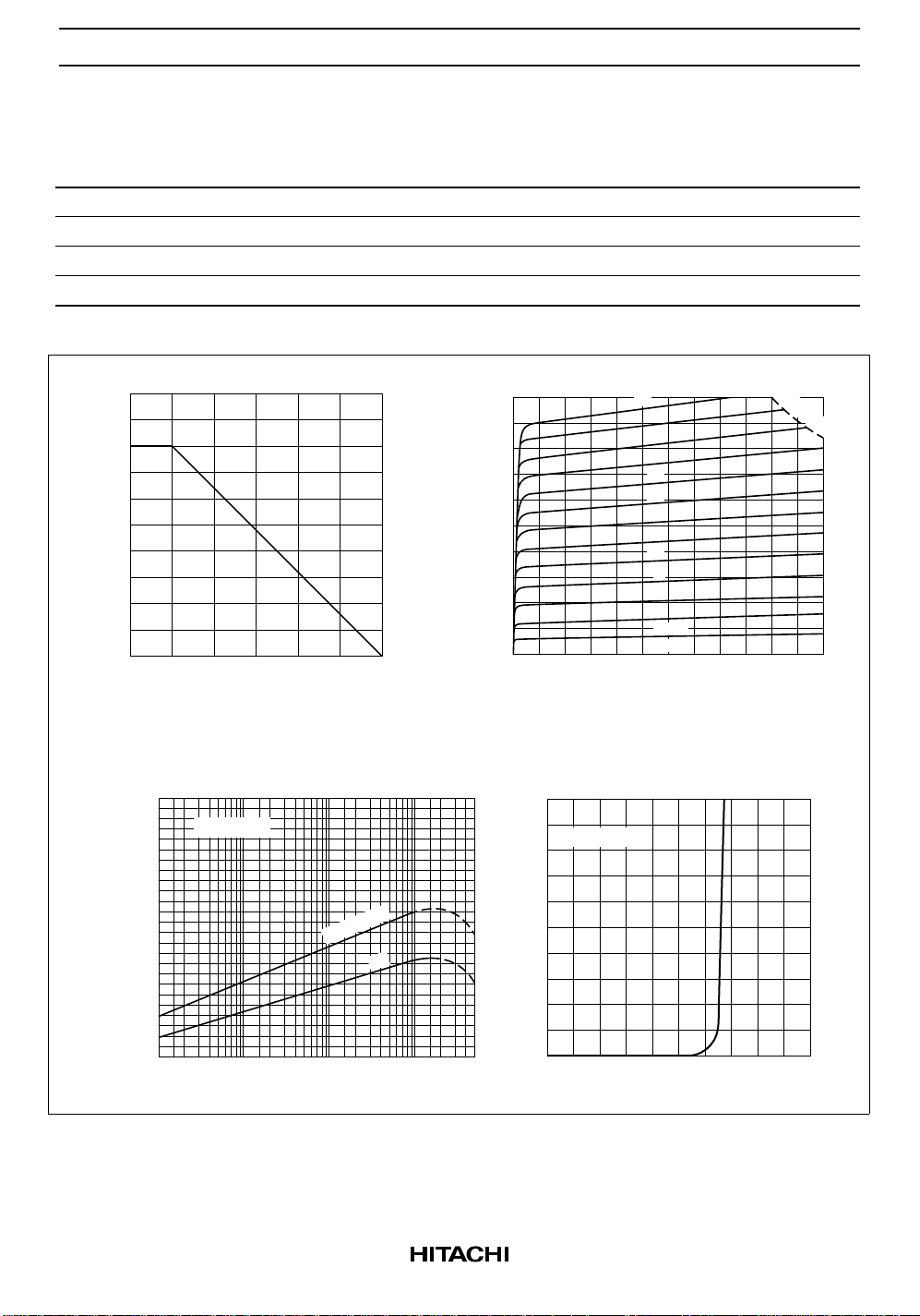
Maximum Collector Dissipation Curve
250
(mW)
200
C
150
100
50
Collector Power Dissipation P
0
700
FE
600
500
50
Ambient Temperature Ta (°C)
DC Current Transfer Ratio vs.
Collector Current
VCE = 12 V
100 150
10
8
(mA)
C
6
4
2
Collector Current I
0
(mA)
Typical Output Characteristics
Collector to Emitter Voltage V
Typical Transfer Characteristics
5
VCE = 12 V
4
C
3
26
24
22
20
18
16
14
12
10
8
6
4
2 µA
IB = 0
84
12 16 20 24
CE
(V)
P
C
= 200 mW
400
300
DC Current Transfer Ratio h
200
0.01 0.02 0.05 0.1 0.2 0.5 1.0 2 5 10 20 50
Collector Current I
Ta = 75°C
25
(mA)
C
2
1
Collector Current I
0
0.2 0.4
Base to Emitter Voltage V
0.6 0.8 1.0
(V)
BE
3
 Loading...