

Hetronic CSM400UE User Manual

R&D
Technical
Documentation
Revision
A
B
C June25-2015 BG
D July6-2015 BG
E July8-2015 BG RF Transceiver module / Sub 1GHz
F Aug11-2015 BG
G Aug26-2015 BG
H Oct14-2015 BG
I Oct16-2015 BG
J Mar16-2017 GWH
3.3~5.0Vdc / USB Flash programmable
Modified Checked Module Name
Date By Date By
Apr14-2015 BG
Apr24-2015 BG
CSM-400UE
Description
Remarks
Item Number
66990004

1. TABLE OF CONTENTS
1. TABLE OF CONTENTS ................................................................................................................................ 2
2. PROJECT DESCRIPTION ............................................................................................................................. 3
3. BLOCK DIAGRAM ....................................................................................................................................... 4
4. TECHNICAL SPECIFICATION .................................................................................................................... 5
5. CONNECTION DIAGRAM ........................................................................................................................... 6
6. FUNCTIONAL DESCRIPTION ..................................................................................................................... 7
7. ASSEMBLY DESCRIPTION ......................................................................................................................... 8
8. MECHANICAL DRAWING ........................................................................................................................ 10
9. TEST PROCEDURE ..................................................................................................................................... 11
10. SCHEMATIC ............................................................................................................................................ 21
11. PCB ............................................................................................................................................................ 22
12. FIRMWARE .............................................................................................................................................. 24
13. ATTACHMENTS ...................................................................................................................................... 24
14. PARTS LIST .............................................................................................................................................. 25
15. REVISION HISTORY............................................................................................................................... 27
TABLE OF FIGURES
Figure 1: CSM-400UE Block Diagram .................................................................................................................. 4
Figure 2: CSM-400UE Connection Diagram ......................................................................................................... 6
Figure 3: CSM-400UE Top Lacquer Mask ............................................................................................................ 8
Figure 4: CSM-400UE Bottom Lacquer Mask ....................................................................................................... 8
Figure 5: RF Shield Solder Pads ............................................................................................................................. 9
Figure 6: CSM-400UE with Soldered Shield ......................................................................................................... 9
Figure 7: CSM-400UE Mechanical Drawing ....................................................................................................... 10
Figure 8: CSM-400UE Schematic ........................................................................................................................ 21
Figure 9: CSM-400UE PCB Layers ..................................................................................................................... 22
Figure 10: CSM-400UE Top Components ........................................................................................................... 23
Figure 11: CSM-400UE Bottom Components ...................................................................................................... 23
Research and Development
Technical Documentation
Form Rev. A
Revision Project: Page
J
Description: RF Transceiver module / Sub 1GHz 2 of 27

2. PROJECT DESCRIPTION
CSM-400UE is a modular 410-475MHz RF transceiver designed to provide the RF interface for Hetronic
devices. The module is designed to be mounted onto Hetronic coder and decoder boards to convert digital
information to RF signals and RF signals to digital information. CSM-400UE can be programmed to
function in several different operating modes. Configuring the operating mode and functional settings of
each mode allows CSM-400UE to be expandable to additional operating modes, new RF protocols and
many frequency channels. CSM-400UE communicates with a PC using the CSM-CFG board as an USB and
RS-232 adapter.
CSM-400UE uses an internal 3.1V regulator and requires a 3.3-5.0V external power supply. Absolute
maximum survival supply voltage is limited to 12VDC. In applications, this will be provided by the host
coder/decoder board. CSM-400UE can be configured to operate on any 6.25kHz channel from 410MHz 475MHz. The RF output power is set to 10dBm (10mW). Depending on the protocol, CSM-400UE can
operate at RF baudrates up to 50kbps. CSM-400UE is built around the TI CC1200 Sub-1GHz RF
transceiver. RF front-end circuitry on the device limits effective performance to ~385MHz to ~500MHz,
although the hard frequency limits for the 400 MHz range are from 410 to 475 MHz. RF sensitivity varies
depending on the protocol being used.
All of the functionality of the CSM-400UE is configured in the firmware. CSM-CFG is also used to load the
firmware bootloader over RS-232 and firmware application using the USB Flash Programmer tool. CSM400UE can also connect to the PC H-Link tool over the CSM-CFG board. H-Link serves an important
purpose for CSM-400UE: calibrating the on-board radio. Every CSM-400UE module must be calibrated
before use in a Hetronic product. H-Link calibration compensates for production variation in the RF
performance of the on-board radio.
CSM-400UE by default is configured to 'ELP-TRx' mode. This causes it to act as a transceiver for the
Hetronic ELP protocol. In this mode it will only communicate with other ELP devices. In ELP Mode, radio
control and data transfer are all handled over the DI and DO pins with 115.2k baud UART. The legacy 'AF'
pin does not support audio output but is instead used for USB detection. CSM-400UE's frequency and
encryption can be configured using the CSM Configuration Tool. For more information, see the CSM_CFG
Technical Document.
Research and Development
Technical Documentation
Form Rev. A
Revision Project: Page
J
Description: RF Transceiver module / Sub 1GHz 3 of 27

3. BLOCK DIAGRAM
Figure 1: CSM-400UE Block Diagram
Research and Development
Technical Documentation
Form Rev. A
Revision Project: Page
J
Description: RF Transceiver module / Sub 1GHz 4 of 27
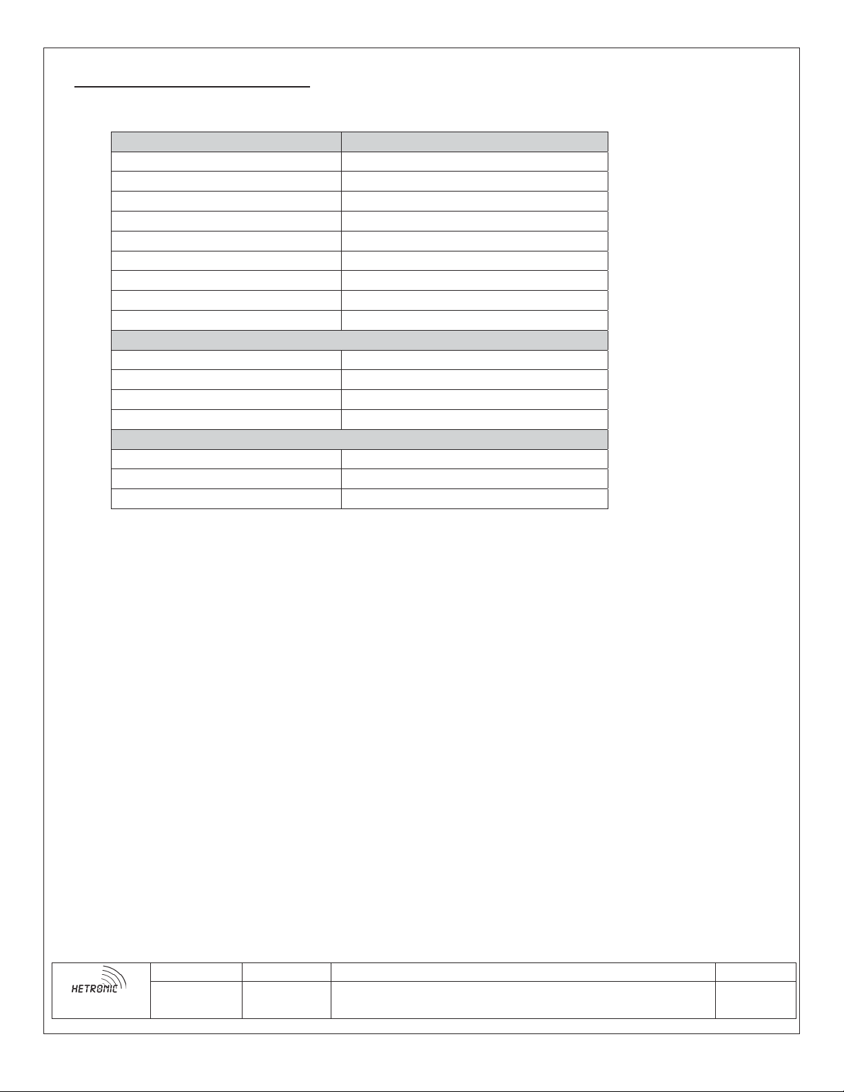
4. TECHNICAL SPECIFICATION
Parameter Specification
Nominal Supply (BATT+) 3.2~5.0Vdc
Max Supply (BATT+) 5.5V
Min Supply (BATT+) 2.9Vdc
Max Input Voltage on I/O pins 5Vdc
Operating Temperature Range -40°C ~ +80°C
Operating Frequency Range 410.0000MHz ~475.0000MHz
Channel Step 6.25 kHz minimum
Max Data Rate 50 kbps maximum
Antenna / Impedance SMB / 50ohms
TRANSMITTER - ELP
TX Operating Current 60mA
RF Output Power -10 to +10dBm (configurable)
Frequency Deviation 14 kHz (ELP, 4-GFSK, 50 kbps)
Spurious emission > -40dB
RECEIVER - ELP
RX Operating Current 60mA
Sensitivity -103 dBm (ELP, 4-GFSK, 50 kbps)
Adjacent Channel Selectivity 65dB
Research and Development
Technical Documentation
Form Rev. A
Revision Project: Page
J
Description: RF Transceiver module / Sub 1GHz 5 of 27
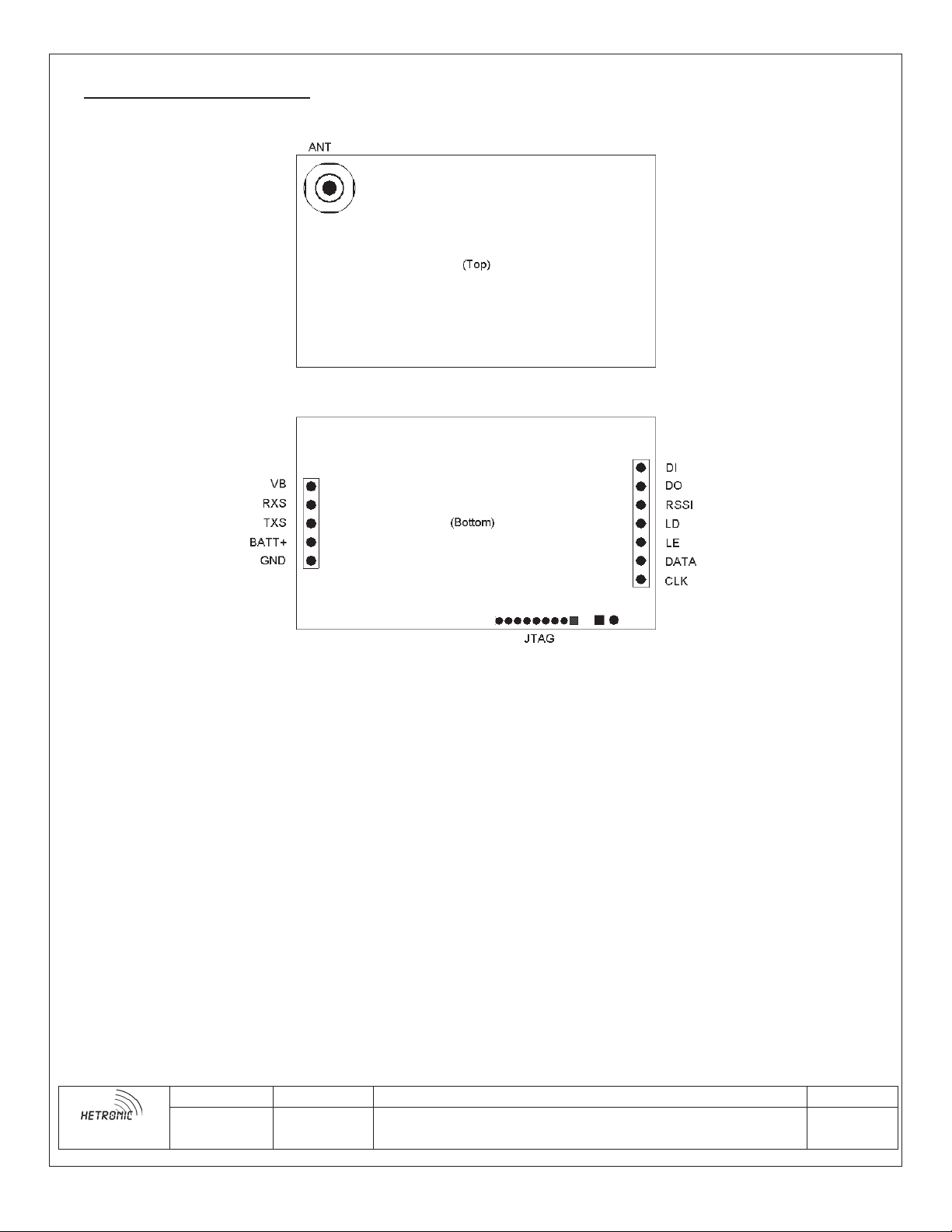
5. CONNECTION DIAGRAM
Research and Development
Technical Documentation
Form Rev. A
Figure 2: CSM-400UE Connection Diagram
Revision Project: Page
J
Description: RF Transceiver module / Sub 1GHz 6 of 27
 Loading...