

Page 1
CONFIDENTIAL
PA-1
User Manual
Revision
In-Line, Bi-Directional RF switching module for 420 to
Modified Checked Module Name
Date By Date By
PA-1
Description
475MHz. PA-1 includes a 120mW RF Power Amplifier for
the transmit direction and a SAW filter with LNA for the
receive direction.
Remarks
Item Number
52450041
Page 2

CONFIDENTIAL
1. TABLE OF CONTENTS
1. TABLE OF CONTENTS ................................................................................................................................ 2
2. PROJECT DESCRIPTION ............................................................................................................................. 3
3. TECHNICAL SPECIFICATION .................................................................................................................... 4
4. FUNCTIONAL DESCRIPTION ..................................................................................................................... 4
5. PCB .................................................................................................................................................................. 5
TABLE OF FIGURES
Figure 1, PA-1 PCB Layers .................................................................................................................................... 5
Figure 2, PA-1 Top Components (left); Bottom Components (right) .................................................................... 6
Page 3

2. PROJECT DESCRIPTION
CONFIDENTIAL
PA-1 is an in-line, Bi-Directional RF switching module for 420 to 475MHz. It includes a 120mW RF
Power Amplifier for the transmit direction and a SAW filter with LNA for the receive direction. In addition
to the item number, check-boxes are provided to indicate power output level. When the Control Input line is
low (typically below 1V), the module is in Receive Mode. When the Control Input is high (typically above
1.2V), the module is in Transmit Mode. The PA-1 typically operates from a 5Vdc supply or battery voltage
down to 3.5Vdc. Test Pad PD is a Power Detector output that provides an analog voltage that is
proportional to the transmit output power.
FCC ID: LW9-PA1
IC ID: 2119B-PA1
Note: Operation is subject to the following two conditions: (1) this device may not cause interference,
and (2) this device must accept any interference, including interference that may cause undesired
operation of the device.
Note: The user is cautioned that changes or modifications not expressly approved by the party
responsible for compliance could void the user’s authority to operate the equipment.
Note: The antenna(s) used for this transmitter must be installed to provide a separation distance of at
least 20cm from all persons. The antenna(s) used for this transmitter must not transmit
simultaneously with any other antenna or transmitter, except in accordance with FCC and IC multitransmitter product procedures.
Note: Under Industry Canada regulations, this radio transmitter may only operate using an antenna
of the same type and equal or lesser gain approved for the transmitter by Industry Canada. To reduce
potential radio interference to other users, the antenna type and its gain should be so chosen that the
equivalent isotropically radiated power (e.i.r.p.) is not more than that necessary for successful
communication.
Remarque : L'opération est soumis à deux conditions suivantes: (1) ce dispositif ne peut pas causer de
brouillage, et (2) ce dispositif doit accepter toute interférence, y compris le brouillage qui peut causer
intempestif de fonctionnement du dispositif.
Remarque : L'utilisateur est averti que les changements ou modifications non expressément
approuvées par la partie responsable de la conformité pouvaient annuler l'autorisation l'utilisateur à
faire fonctionner l'équipement.
Remarque : L'utilisation utilisée pour cet émetteur doit être installée pour fournir une distance de
séparation d'au moins 20 cm de toutes les personnes. L'utilisation utilisée pour cet émetteur ne doit
pas transmettre simultanément avec une autre antenne ou émetteur, sauf conformément aux
procédures de produits multi-transmitter de FAC et IC.
Page 4
3. TECHNICAL SPECIFICATION
CONFIDENTIAL
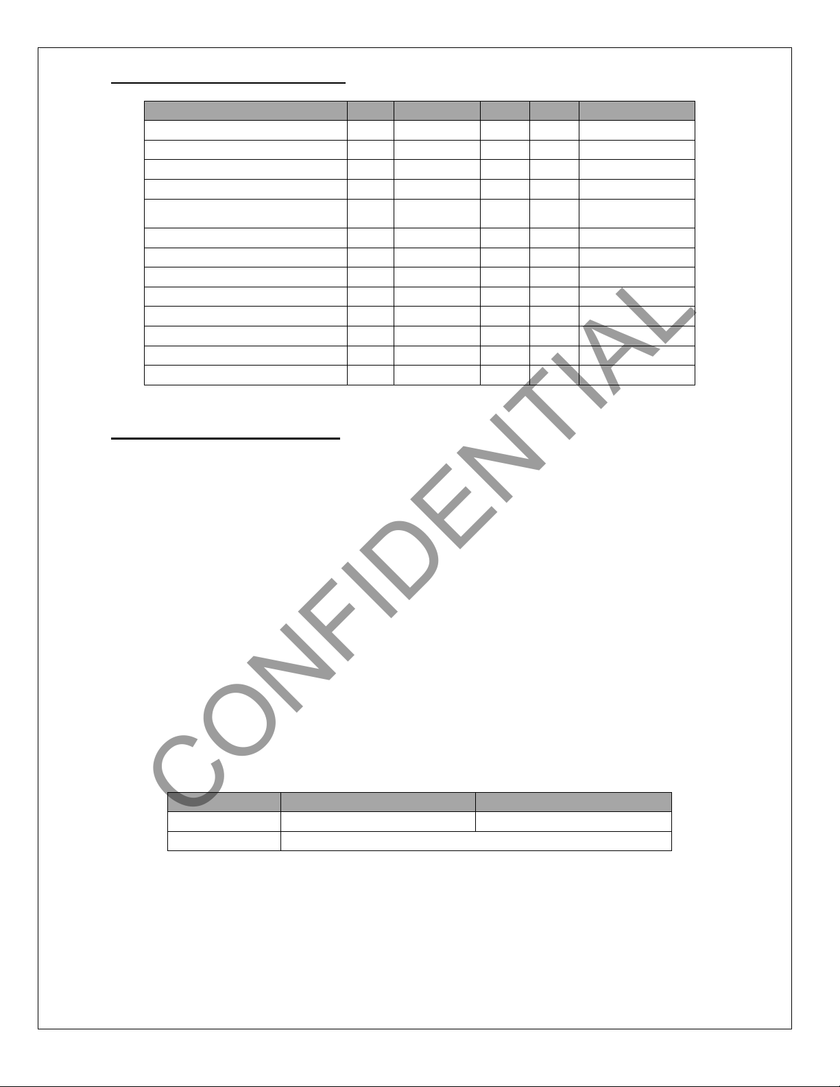
Parameter Min. Typ. Max. Unit Notes
Supply Voltage 3.5 4.0 6.0 Vdc
Supply Current TX 120mW 180±10% mA 50 ohm load
Supply Current RX 1.0 mA
TX Frequency Range 420 475 MHz
RX Frequency Range 450 472 MHz
RF Output Power 19 20.8 dBm 10dBm input
RF Receive Signal Gain 20±10% dB
Switching Time RX to TX 0.5 mS
Switching Time TX to RX 0.3 mS
Control Input High 1.2 12.0 Vdc TX Mode
Control Input Low -2.0 1.0 Vdc RX Mode
Operating Temperature -30º 85º C
4. FUNCTIONAL DESCRIPTION
Limited by Rx
SAW filter.
4.1. Operation
When the logic level on the Control Input line is low (typically below 1V), the module is in receive
mode. The RF switches are configured to route the incoming RF signal from the antenna through a
SAW filter and Low Noise Amplifier (LNA) for increased sensitivity. The SAW filter allows only
in-band signals to pass, therefore out of band interference is reduced significantly. SAW filters may
be changed to accommodate frequencies within the TX frequency range other than 450 to 472 MHz,
or omitted in favor of external band pass filters. Aside from boosting the incoming signal, the LNA’s
amplification helps to offset the signal loss from the SAW filter and lengths of cable. The amplified
signal is connected to the RF module via the onboard SMB connector marked X2.
When the logic level on the Control Input line is high (typically above 1.2V), the module is in
transmit mode. The RF switches are configured to route the transmitted signal from the RF module
to the PA-1 Power Amplifier. The Power Amplifier boosts the transmitted signal power. After the
PA, the amplified signal is fed through a Low Pass Filter to suppress harmonics. The amplified signal
is then fed to the antenna via the onboard SMB connector marked ANT. Test Pad PD is a Power
Detector output that provides an analog voltage proportional to the transmit output power.
Solder Jumper UP DOWN
Closed 11KΩ pull-up to +3.3Vdc 9KΩ pull-down to Ground
Open Default, 100K pull-down
Page 5
CONFIDENTIAL
5. PCB
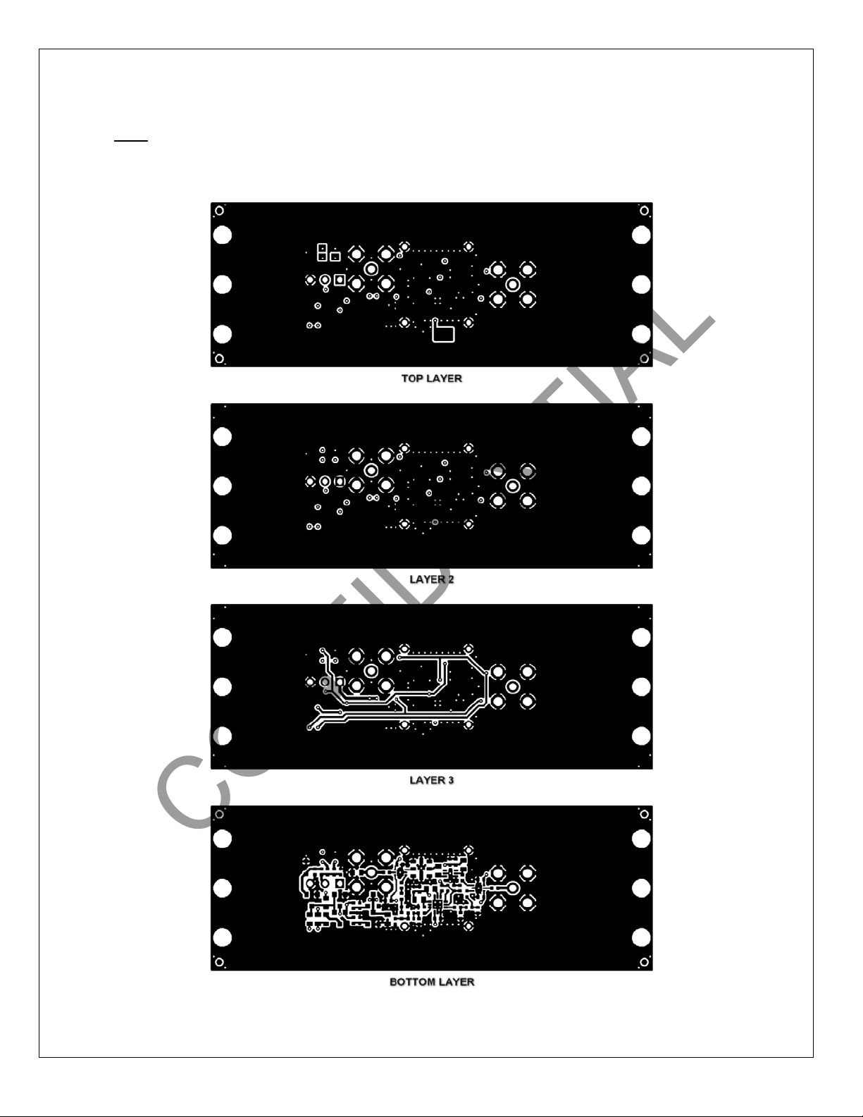
5.1. PCB Layers
Figure 1, PA-1 PCB Layers
Page 6
CONFIDENTIAL
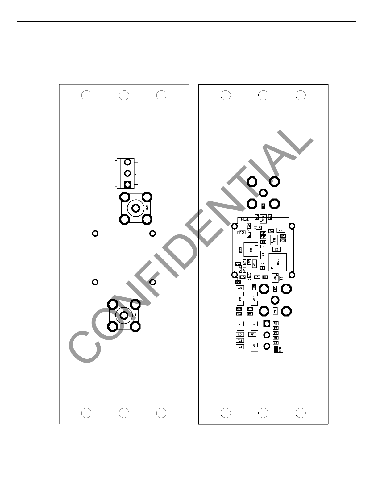
5.2. Component Placement
Figure 2, PA-1 Top Components (left); Bottom Components (right)
 Loading...