


harman/kardon |
Service Manual |
HK 990/230
2 x 200W INTEGRATED STEREO AMPLIFIER
Released EU2009 |
harman/kardon, Inc. |
Rev 0, 03/2009 |
|
250 Crossways Park Dr. |
|
|
Woodbury, New York, 11797 |
|
CONTENTS |
|
|
||
1. |
Specification |
................................................................................................................................ |
1 |
|
2. |
Front |
panel |
information ..................................................................................................................... |
2 |
3. |
Rear |
panel ............................................................................................... |
information |
3 |
4. |
Remote control ..................................................................................................information |
4 |
||
5. |
AMP |
Adjustment............................................................................................................ |
5 |
|
6. |
Wiring |
diagrams..................................................................................................................... |
6 |
|
7. |
IC spec............................................................................................................................. |
|
7-79 |
|
8. |
Printed circuit boards................................................................................................................................................. |
80-99 |
||
9. |
Schematic diagram.................................................................................................................................................100-124 |
|||
10. Exploded view......................................................................................................................................................... |
|
125-126 |
||
11. |
Electrical parts ..................................................................................................................................................list |
126-139 |
||

Specifications
|
|
NOMINAL |
Continuous Average Power Per Channel (FTC) |
8 Ohms: |
150 Watts@<0.03%THD |
20 Hz – 20 kHz, both channels driven |
4 Ohms: |
300 Watts@<0.3%THD |
Dynamic Power (IHF, 1 kHz Tone Burst) |
8 Ohms: |
220 Watts |
|
4 Ohms: |
440 Watts |
High instantaneous current capability (HCC) |
|
±200 Amps |
Power Bandwidth @ Half-Rated output, 81 |
|
20 Hz - 100 kHz |
Frequency response @ 1W (+0/-3dB) |
|
5 Hz - 120 kHz |
Damping factor (20Hz-20k Hz) |
|
>200 |
Signal-to-noise Ratio (Reference rated power output, A-WTD) |
Tuner/CD |
100 dB |
|
Phono (MC): |
75 dB |
Input sensitivity/Impedance |
Tuner/CD |
350 mV/43k Ohms |
|
Phono (MM): |
10 mV/47k Ohms |
|
Phono (MC): |
1 mV/100 Ohms |
Overload |
Tuner/CD |
2.8V |
|
Phono (MM): |
85 mV |
|
Phono (MC): |
8.5 mV |
Tone control range, Bass @ 100 Hz/Treble @ 10 kHz |
|
±10 dB/±10 dB |
Power supply |
|
AC 230V, 50 Hz |
Power consumption |
|
1000 W |
Standby power consumption |
|
1W |
Dimensions (Width x Height x Depth) |
|
440 x 160 x 444 mm |
Depth includes Volume Button and Loudspeaker Terminals |
|
|
Weight |
|
24 kg |
250 Crossways Park Drive, Woodbury, New York 11797 www.harmankardon.com
Harman Consumer Group International:
2, Route de Tours, 72500 Château-du-Loir, France © 2008 Harman Kardon, Incorporated
Part no. 8509 9012 0000
1
Controls and Functions
|
|
|
|
|
|
|
|
|
|
|
|
|
|
|
Power Indicator: This LED will illuminate in amber when the unit is in the Standby mode to signal that the unit is ready to be turned on. When the unit is in operation, the indicator will turn white.
System Power Control: Press this button to turn on the HK 990; press it again to turn the unit off (to Standby). Entering Standby also saves all Setup parameters.
Speaker 1/2 Selectors: Press to select speaker pair 1 or 2, or both, or neither (headphone output only).
Record Out Selector: First press shows the record source presently selected in the display. Pressing on the the Source selectors within
a few seconds after pressing changes the record source. Exit this function by pressing again, or wait for a few seconds until exit takes place automatically.
Input Source Selector: Select input source for listening by pressing one of the ”Source” buttons repeatedly to scroll through all the Inputs either forwards or backwards, until the display shows the desired source.
Input Setup Button: Press this Button to enter/exit the Input Setup Mode. Here you can select the physical connection for each source (Analog/Digital etc.) as well as Gain, Bass/Treble etc. Refer to the Setup section of this manual.
Speaker Setup Selector: Press this Button to enter the Speaker Setup Menu, where you can switch subwoofers on and off, select crossover frequency, run automatic speaker setup (EzSet/EQ) etc. Refer to the Setup section of this manual.
Up/Down Arrow Buttons: Press to scroll through various options for adjustment in a menu.
Left/Right Arrow Buttons: Press to increase/decrease a parameter or to select between parameters after selecting a menu for adjustment with the Up/Down Arrow Buttons.
Level Settings Button: Press to enter/exit the Balance left/right adjustment for the speakers as well as subwoofer level.
Headphone Jack/Setup Microphone Input: Plug in headphones if desired. With both ”Speaker 1” and ”2” selectors in the Off position, output is supplied only to headphones. When using the automatic loudspeaker setup and calibration system (EzSet/EQ), plug the microphone in here.
Volume Control: Turn to raise or lower output volume.
Remote Sensor Window: The sensor behind this window receives infrared signals from the remote control. Aim the remote at this area and do not block or cover it unless an external remote sensor is installed.
Enter Button: Press to select a parameter for adjustment and to confirm.
Main Information Display: This display delivers messages and status indications to help you operate the amplifier.
CONTROLS AND FUNCTIONS
2
Connections
|
|
|
|
|
|||||||||||||
|
|
|
|
|
|
|
|
|
|
|
|
|
|
|
|
|
|
|
|
|
|
|
|
|
|
|
|
|
|
|
|
|
|
|
|
|
|
|
|
|
|
|
|
|
|
|
|
|
|
|
|
|
|
|
|
|
|
|
|
|
|
|
|
|
|
|
|
|
|
|
|
|
|
|
|
|
|
|
|
|
|
|
|
|
|
|
|
|
|
|
|
|
|
|
|
|
|
|
|
|
|
|
|
|
|
|
|
|
|
|
|
|
|
|
|
|
|
|
|
|
|
|
|
|
|
|
|
|
|
|
|
|
|
|
|
|
|
|
|
|
|
|
|
|
|
|
|
|
|
|
|
|
|
|
|
|
|
|
|
|
|
|
|
|
|
|
|
|
|
|
|
|
|
|
|
|
|
|
|
|
|
|
|
|
|
|
|
|
|
|
|
|
|
|
|
|
|
|
|
|
|
|
|
|
|
|
|
|
|
|
|
|
|
|
|
|
|
|
|
|
|
|
|
|
|
|
|
|
|
|
|
|
|
|
|
|
|
|
|
|
|
|
|
|
|
|
|
|
|
|
|
|
|
|
|
|
|
|
|
|
|
|
|
|
|
|
|
|
|
|
|
|
|
|
|
|
|
|
|
|
|
|
|
|
|
|
|
|
|
|
|
|
|
|
|
|
|
|
|
|
|
|
|
|
|
|
|
|
|
|
|
|
|
|
|
|
|
|
|
|
|
|
|
|
|
|
|
|
|
|
|
|
|
|
|
Right Loudspeaker output, System 2.
Right Loudspeaker output, System 1.
RS-232 connector for possible future PC update. Update Switch.
Input jacks for one or two subwoofer signals from external surround processor.
Output jacks for two subwoofers.
Digital coaxial output jack for digital recording. Also permits digital recording of analog sources.
Preamplifier output jacks.
Analog output jacks for tape recording.
Analog output jacks for CD Recorder analog recording.
AUX input jacks, suitable for analog signals from video games, video recorders etc.
TV input jacks for analog sound input from your TV.
TAPE input jacks for analog tape replay.
CDR input jacks, for CD Recorder analog replay.
Balanced analog inputs (XLR), for use with all signal sources that output balanced signals. Available via the CD Input function only, as
an alternative to the unbalanced RCA jacks (Input ). Pin configuration for the XLR Inputs: Pin 1 is Ground, Pin 2 is Plus/Hot, Pin 3 is Minus/Cold.
Left Loudspeaker output, System 2.
Left Loudspeaker output, System 1.
Power lead AC input.
TUNER analog Input jacks.
PROCESSOR Analog Inputs. These Inputs go directly to the power amplifier section of the HK 990, bypassing the Volume and Tone Control. Here you can connect the Front Channel Pre Out L+R signals from an external surround processor, to benefit from
the superior power of the HK 990 and control volume from the processor. NOTE: Only use the Processor Input with a device that has its own volume control!
CD analog Input jacks. You can select either this Input or the Balanced Input as analog Input in the CD Input Setup Mode.
Phono Input for record player with Moving Magnet (high output and high impedance) or High-Output Moving Coil cartridge.
Phono Input for record player with Moving Coil (low output and low impedance) cartridge.
If your record player has a separate Ground wire, attach it here to avoid hum noise.
Connect the trigger Input (if available) on one or two subwoofers to these trigger ON/ OFF output jacks. When you switch ON the HK 990, it sends a trigger signal, which switches ON the subwoofer. When switching OFF the HK 990, the subwoofer also switches OFF.
HRS (High-Resolution Synchronization) Input. Use the included HRS-cable to connect the HD 990 CD player (or other similarly equipped player) for optimum sound quality.
Optical Digital Inputs (TOS-Link). Connect any digital device with Optical Digital Output to one of these Inputs. Push the Optical Jack through the hinged door that covers the Input until it clicks into place.
Coaxial Digital Inputs. Connect any digital device with Coaxial Digital Output to one of these Inputs. Usually, Coaxial Digital transmission is preferred to Optical, given a choice.
Remote IN. To control your HK 990 with an external infrared remote sensor, connect the wire from the remote sensor here.
Remote OUT. Connect other Harman Kardon devices (you may also experiment with other brands) that you wish to control with the HK 990 Remote Control to this Output.
CONNECTIONS
3
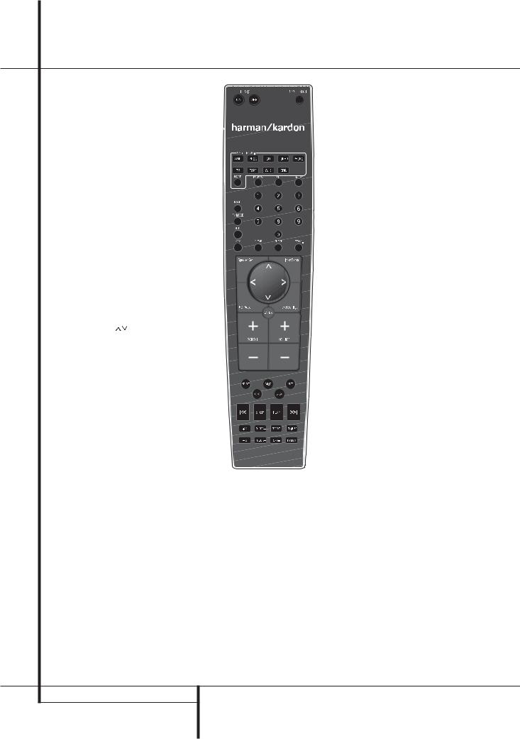
Remote Control
Band: Switches between frequency bands on a Tuner.
FM Mode: Switches between Stereo and Mono on a Tuner.
Auto: Switches between Automatic and Manual tuning on a Tuner.
Mem: For memorizing a radio station in the Preset Memory of a Tuner.
Clear: Clears the memory of a CD/CDR or clears a preset from Tuner station list.
Check: Press this button to check the order of tracks programmed into a CD player’s memory.
Prog: Press this button to begin the process of programming a CD player to play the tracks of a disc in a specific order.
Speaker Setup: Press to enter the HK 990 Speaker Setup functions. See below for explanation of the Speaker Setup process.
Input Setup: Press to enter the HK 990 Input Setup functions. See below for explanation of the Input Setup process.
Arrow Buttons (FeEee): This round button is used to navigate within the menus of the HK 990.
EQ Preset: Press to enter the HK 990 Equalizer Preset functions. See below for explanation of the EQ Presets.
Level Settings: Press to enter the HK 990 Level Setting functions. See below for explanation of the Level Setting process.
Enter: Press to confirm a selection within a HK 990 setup procedure or to switch between
selections. See under each Setup process for further explanations.
Scroll ZdI: When listening to a Tuner, press + to tune to higher frequency stations and – to tune to lower frequency stations. Also see the Owners Manual for your harman/kardon tuner.
Volume ZdI: Press to adjust the HK 990 volume up or down.
Select: When listening to a tuner, press this button to alternate between Auto Tune, Manual Tune or Preset Tune.
Pause: When playing a CD, press this button to momentarily pause the disc. Press again to resume play.
Mute: Press this button to momentarily silence the HK 990. “Muted” flashes in the front panel display. Press again to re-activate sound output.
EEand FF(Search Buttons): Press one of these buttons to search fast forward or backward on a CD or Tape. You can hear intermittent sounds from the CD while searching. Normal playback resumes when you release the button.
.EEand FF.(Skip Buttons): Press one of these buttons to move to the next track or to the previous track on a CD or Tape. Repeatedly pressing one of the buttons skips more tracks. On a CD, pressing Skip Forward while playing the last track skips to track 1, and pressing Skip Back while playing track 1 skips to the last track.
Stop: Press this button to stop play of a CD or Tape.
Play: Press this button to start playback of a CD or Tape. If the CD drawer is open, the drawer closes and play begins. Pressing the Play Button again pauses play momentarily, same as the Pause Button.
Z10 and I10: When playing a CD, press the +10 Button to skip 10 tracks forward and the -10 Button to skip 10 tracks backward from the track you are playing. More presses again skips 10 more tracks. If there are less than 10 tracks to the end or start of the CD, the last or first track is played.
Folder Zand Folder Ie: When playing a CD with MP3 files, these buttons move to the next or the previous folder with MP3 material.
Repeat: When playing a CD, pressing this button once repeats the current track, shown as “Rep 1” in the CD player’s display. Pressing once more repeats the entire CD, shown as “Rep All” in the CD player’s display. Third press exits repeat play.
Repeat A-B: When playing a CD, press once to establish a starting point (shown as “Rep A” in the CD player’s display) and a second time to establish an end point (shown as Rep A-B in the CD player’s display). The music between these two points is repeated as a loop until you press the button a third time, returning to normal play.
Open/Close: Opens the CD drawer when it is closed and closes it when it is open. The drawer may also be closed by pressing Play.
Random: When playing a CD, press this button to play all tracks in random order.
REMOTE CONTROL
4
AMP Adjustment
Iding Adjustment
Precaution for handling measuring instrument
The ground side of the measuring instrument to be connected to the speaker terminal of this unit must be kept in floating condition because this unit is equiped with the floating balanced power amplifier.
Condition
*Start adjustment 5 minutes or more after the power is turned on.
*Non loaded condition.
Idling Adjustment
Adjust R53 so that the DC voltage of TP1 becomes +38mV .
5
 R53
R53
TP1
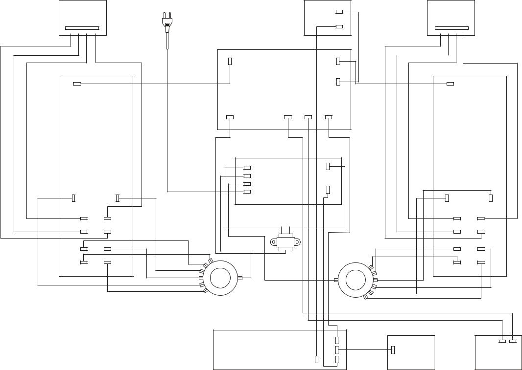
Speaker Board |
Power Cord in |
|
|
|
3P |
Seaker Board |
|
||||||
|
|
|
|
|
|
||||||||
|
|
|
|
|
|
|
In Board |
|
|
|
|
|
|
Sp1+ Sp1Sp2- Sp2+ |
|
|
|
|
|
Sp1+ Sp1Sp2- Sp2+ |
|
||||||
1 |
2 |
3 |
4 |
|
|
|
|
5P CN12 |
1 |
2 |
3 |
4 |
|
|
|
|
|
|
|
||||||||
|
|
|
|
|
7P |
|
|
7P |
|
|
|
|
|
|
|
|
|
|
J2 |
|
|
J3 |
|
|
|
|
|
|
|
|
|
|
|
Preamplifer Board |
|
3P |
|
|
|
|
|
|
7P J1 |
|
|
|
|
|
|
|
|
7P J1 |
|
|
|
|
|
|
|
5P |
|
4P |
5P |
6P |
|
|
|
|
|
|
|
|
|
J11 |
|
J14 |
J13 |
J12 |
|
|
|
|
|
|
|
|
AMP |
|
|
|
|
|
|
|
|
AMP |
|
|
|
|
left |
|
|
|
|
|
|
|
|
right |
|
|
|
|
power |
|
|
|
|
|
|
|
|
power |
|
|
|
|
|
|
2P |
|
|
5P |
|
|
|
|
|
|
|
|
|
|
|
|
CN11 |
|
|
|
|
|
|
|
|
|
|
|
CN7 |
|
|
|
|
|
|
|
|
|
|
|
|
|
|
|
|
|
|
|
|
|
|
6 |
|
|
|
|
2P |
|
|
|
|
|
|
|
|
|
|
|
|
CN8 |
|
|
|
|
|
|
|
|
|
|
|
|
|
|
|
|
|
|
|
|
|
|
|
|
|
|
|
|
2P |
|
|
|
|
|
|
|
|
|
|
|
|
|
CN9 |
Fuse Board |
|
7P |
|
|
|
|
|
|
|
|
|
|
2P |
|
|
|
|
|
|
||
|
|
|
|
|
|
|
CN6 |
|
|
|
|
|
|
|
|
|
|
|
CN10 |
|
|
|
|
|
|
|
|
|
|
|
|
|
|
|
|
|
|
|
|
|
|
|
JP2 |
|
JP8 |
|
|
|
|
|
|
JP2 |
JP8 |
|
|
|
|
JP1 |
|
JP10 |
|
|
|
|
|
|
JP1 |
JP10 |
|
|
|
JP7 |
|
JP9 |
|
|
|
|
|
|
JP7 |
JP9 |
|
|
|
JP4 |
|
JP6 |
|
|
|
|
|
|
JP4 |
JP6 |
|
|
|
JP3 |
|
JP5 |
|
Transformer |
|
|
|
|
JP3 |
JP5 |
|
|
|
|
|
|
|
|
|
|
|
||||
|
|
|
|
Thermistor |
|
|
|
|
Thermistor |
|
|
|
|
|
|
|
|
|
|
|
|
|
|
|
|
|
|
|
|
|
|
|
|
|
|
6P |
|
|
|
|
|
|
|
|
|
|
|
|
|
CN2 |
|
|
|
5P |
4P |
|
|
|
|
|
|
|
|
|
|
|
|
||
|
|
|
|
|
Display Board |
|
4P |
4P |
|
|
CN12 |
CN13 |
|
|
|
|
|
|
|
CN4 |
CN3 |
|
|
Head Phone |
|||
|
|
|
|
|
|
|
5P |
7P |
Led Board |
|
|
||
|
|
|
|
|
|
|
CN3 |
CN1 |
|
|
|
|
|
a |
High Performance Multibit - DAC |
|
with SACD Playback |
||
|
|
AD1955ARS |
FEATURES
5 V Power Supply Stereo Audio DAC System Accepts 16-/18-/20-/24-Bit Data
Supports 24-Bit, 192 kHz Sample Rate PCM Audio Data Supports SACD Bit Stream and External Digital Filter
Interface
Accepts a Wide Range of PCM Sample Rates Including: 32 kHz, 44.1 kHz, 48 kHz, 88.2 kHz, 96 kHz, and
192 kHz
Multibit Sigma-Delta Modulator with "Perfect Differential Linearity Restoration" for Reduced Idle Tones and Noise Floor
Data Directed Scrambling DAC––Low Sensitivity to Jitter Supports SACD Playback with "Bit Expansion" Filter Differential Current Output for Optimum Performance 8.64 mA p-p Differential Output
120 dB SNR/DNR (not muted) at 48 kHz Sample Rate (A-Weighted Stereo)
123 dB SNR/DNR (Mono) –110 dB THD + N
110 dB Stop-Band Attenuation with 0.0002 dB
Pass-Band Ripple
8 Oversampling Digital Filter
On-Chip Clickless Volume Control Supports SACD-Mute Pattern Detection
Supports 64 fS/128 fS DSD SACD with Phase Mode Internal Digital Filter Pass-Through for External Filter Master Clock: 256 fS, 512 fS, 768 fS
Hardware and Software Controllable Clickless Mute Serial (SPI) Control for Serial Mode, Number of Bits,
Sample Rate, Volume, Mute, De-Emphasis, Mono Mode Digital De-Emphasis for 32 kHz, 44.1 kHz, and 48 kHz
Sample Rates
Flexible Serial Data Port with Right-Justified, LeftJustified, I2S, and DSP Modes
28-Lead SSOP Plastic Package
APPLICATIONS
High End DVD Audio
SACD
CD
Home Theater Systems
Automotive Audio Systems
Sampling Musical Keyboards
Digital Mixing Consoles
Digital Audio Effects Processors
REV. 0
Information furnished by Analog Devices is believed to be accurate and reliable. However, no responsibility is assumed by Analog Devices for its use, nor for any infringements of patents or other rights of third parties that may result from its use. No license is granted by implication or otherwise under any patent or patent rights of Analog Devices.
FUNCTIONAL BLOCK DIAGRAM
|
MASTER |
CONTROL |
DSD |
|
|
BITSTREAM |
|||
|
CLOCK INPUT |
DATA INPUT |
INPUT |
|
|
|
|
3 |
4 |
|
AUTO-CLOCK |
|
DIGITAL |
|
|
SPI CONTROL |
SUPPLY |
||
|
DIVIDER |
|
||
|
|
|
||
16-/20-/24-BIT |
3/4 |
|
|
|
AUDIO DATA/ |
MUX |
DSD FILTER |
||
EXTERNAL |
|
|||
DIGITAL |
|
|
|
|
FILTER INPUT |
|
|
|
|
|
SERIAL DATA |
EXTERNAL |
RESET |
|
|
INTERFACE |
FILTER I/F |
||
|
|
|
|
MUTE |
|
DIGITAL |
S/H |
|
|
|
FILTER ENGINE |
|
||
|
|
ANALOG |
||
|
|
|
|
|
|
|
|
|
SUPPLY |
|
NOISE-SHAPED |
MULTIBIT - |
ZERO |
|
|
FLAGS |
|||
|
SCRAMBLING |
MODULATOR |
||
|
|
|||
|
|
|
VOLTAGE |
|
|
I-DAC |
I-DAC |
REFERENCE |
|
|
L-CH |
R-CH |
|
|
|
DIFFERENTIAL |
|
|
|
|
CURRENT OUTPUT |
|
|
|
PRODUCT OVERVIEW
The AD1955 is a complete, high performance, single-chip, stereo digital audio playback system. It is comprised of a multibit sigmadelta modulator, high performance digital interpolation filters, and continuous-time differential current output DACs. Other features include an on-chip clickless stereo attenuator and mute capability, programmed through an SPI compatible serial control port. The AD1955 is fully compatible with all known DVD audio formats including 192 kHz as well as 96 kHz sample frequencies and 24 bits. It is also backward compatible by supporting 50 s/ 15 s digital de-emphasis intended for “redbook” compact discs, as well as de-emphasis at 32 kHz and 48 kHz sample rates.
The AD1955 has a very flexible serial data input port that allows for glueless interconnection to a variety of ADCs, DSPs, SACD decoders, external digital filters, AES/EBU receivers, and
(continued on page 12)
One Technology Way, P.O. Box 9106, Norwood, MA 02062-9106, U.S.A.
Tel: 781/329-4700 |
www.analog.com |
Fax: 781/326-8703 |
© Analog Devices, Inc., 2002 |
7

AD1955ARS
ABSOLUTE MAXIMUM RATINGS*
Parameter |
Min |
Max |
Unit |
|
|
|
|
DVDD to DGND |
–0.3 |
6 |
V |
AVDD to AGND |
–0.3 |
6 |
V |
Digital Inputs |
DGND – 0.3 |
DVDD + 0.3 |
V |
Analog Outputs |
AGND – 0.3 |
AVDD + 0.3 |
V |
AGND to DGND |
–0.3 |
+0.3 |
V |
Reference Voltage |
|
(AVDD + 0.3)/2 |
°C |
Soldering |
|
300 |
|
|
|
10 |
sec |
|
|
|
|
PACKAGE CHARACTERISTICS
Package |
Typ |
Unit |
|
|
|
JA (Thermal Resistance |
109.0 |
°C/W |
[Junction-to-Ambient]) |
|
°C/W |
JC (Thermal Resistance |
39.0 |
|
[Junction-to-Case]) |
|
|
|
|
|
*Stresses greater than those listed under Absolute Maximum Ratings may cause permanent damage to the device. This is a stress rating only; functional operation of the device at these or any other conditions above those indicated in the operational section of this specification is not implied. Exposure to absolute maximum rating conditions for extended periods may affect device reliability.
ORDERING GUIDE
Model |
Temperature |
Package Description |
Package Option* |
|
|
|
|
AD1955ARS |
–40°C to +85°C |
28-Lead SSOP |
RS-28 |
AD1955ARSRL |
–40°C to +85°C |
28-Lead SSOP |
RS-28 on 13" Reels |
EVAL-AD1955EB |
|
Evaluation Board |
|
|
|
|
|
*RS = Shrink Small Outline Package
PIN CONFIGURATION
DVDD |
|
|
|
DGND |
1 |
|
28 |
||
LRCLK/EF_WCLK |
|
|
|
MCLK |
2 |
|
27 |
||
BCLK/EF_BCLK |
|
|
|
CCLK |
3 |
|
26 |
||
SDATA/EF_LDATA |
|
|
|
CLATCH |
4 |
|
25 |
||
EF_RDATA |
|
|
|
CDATA |
5 |
|
24 |
||
DSD_SCLK |
|
|
|
PD/RST |
6 |
AD1955 |
23 |
||
DSD_LDATA |
|
|
MUTE |
|
7 |
TOP VIEW |
22 |
||
DSD_RDATA |
|
(Not to Scale) |
|
ZEROL |
8 |
21 |
|||
DSD_PHASE |
|
|
|
ZEROR |
9 |
|
20 |
||
|
|
|
|
|
AGND |
10 |
|
19 |
AGND |
|
|
|
|
|
IOUTR+ |
11 |
|
18 |
IOUTL+ |
|
|
|
|
|
IOUTR– |
12 |
|
17 |
IOUTL– |
|
|
|
|
|
FILTR |
13 |
|
16 |
FILTB |
|
|
|
|
|
IREF |
14 |
|
15 |
AVDD |
|
|
|
|
|
CAUTION
ESD (electrostatic discharge) sensitive device. Electrostatic charges as high as 4000 V readily accumulate on the human body and test equipment and can discharge without detection. Although the AD1955 features proprietary ESD protection circuitry, permanent damage may occur on devices subjected to high energy electrostatic discharges. Therefore, proper ESD precautions are recommended to avoid performance degradation or loss of functionality.
WARNING!
ESD SENSITIVE DEVICE
REV. 0
8
Advanced |
AMS1117 |
Monolithic |
1A LOW DROPOUT VOLTAGE REGULATOR |
Systems |
|
FEATURES |
APPLICATIONS |
• Three Terminal Adjustable or Fixed Voltages* |
• High Efficiency Linear Regulators |
1.5V, 1.8V, 2.5V, 2.85V, 3.3V and 5.0V |
• Post Regulators for Switching Supplies |
• Output Current of 1A |
• 5V to 3.3V Linear Regulator |
• Operates Down to 1V Dropout |
• Battery Chargers |
• Line Regulation: 0.2% Max. |
• Active SCSI Terminators |
• Load Regulation: 0.4% Max. |
• Power Management for Notebook |
• SOT-223, TO-252 and SO-8 package available |
• Battery Powered Instrumentation |
GENERAL DESCRIPTION
The AMS1117 series of adjustable and fixed voltage regulators are designed to provide 1A output current and to operate down to 1V input-to-output differential. The dropout voltage of the device is guaranteed maximum 1.3V at maximum output current, decreasing at lower load currents.
On-chip trimming adjusts the reference voltage to 1%. Current limit is also trimmed, minimizing the stress under overload conditions on both the regulator and power source circuitry.
The AMS1117 devices are pin compatible with other three-terminal SCSI regulators and are offered in the low profile surface mount SOT-223 package, in the 8L SOIC package and in the TO-252 (DPAK) plastic package.
ORDERING INFORMATION:
|
PACKAGE TYPE |
|
OPERATING JUNCTION |
|
|
|
|
TO-252 |
SOT-223 |
8L SOIC |
TEMPERATURE RANGE |
|
|
|
|
AMS1117CD |
AMS1117 |
AMS1117CS |
-40 to 125° C |
AMS1117CD-1.5 |
AMS1117-1.5 |
AMS1117CS-1.5 |
-40 to 125° C |
AMS1117CD-1.8 |
AMS1117-1.8 |
AMS1117CS-1.8 |
-40 to 125° C |
AMS1117CD-2.5 |
AMS1117-2.5 |
AMS1117CS-2.5 |
-40 to 125° C |
AMS1117CD-2.85 |
AMS1117-2.85 |
AMS1117CS-2.85 |
-40 to 125° C |
AMS1117CD-3.3 |
AMS1117-3.3 |
AMS1117CS-3.3 |
-40 to 125° C |
AMS1117CD-5.0 |
AMS1117-5.0 |
AMS1117CS-5.0 |
-40 to 125° C |
*For additional available fixed voltages contact factory.
8L SOIC Top View
GND/ADJ |
|
|
|
N/C |
|||
1 |
|
8 |
|||||
V |
|
|
|
|
|
V |
|
OUT |
2 |
|
7 |
OUT |
|||
|
|
|
|
|
|||
VOUT |
|
|
|
VOUT |
|||
3 |
|
6 |
|||||
|
|
|
|||||
V |
IN |
4 |
|
5 |
N/C |
||
|
|
|
|
|
|
|
|
|
|
|
|
|
|
|
|
PIN CONNECTIONS |
SOT-223 Top View |
|
|
|
||||||||||
3 PIN FIXED/ADJUSTABLE |
|
|
|
|
|
|
|
|
|
|
|
TO-252 FRONT VIEW |
||
|
|
|
|
|
|
|
|
|
|
|
||||
|
|
|
|
|
|
|
|
|
|
|
||||
VERSION |
|
|
|
|
|
|
|
|
|
|
TAB IS |
3 |
|
|
|
|
|
|
|
|
|
|
|
|
|
|
|
||
|
|
|
|
|
|
|
|
|
|
|
2 |
|
|
|
|
|
|
|
|
|
|
|
|
|
|
OUTPUT |
|
|
|
1- Ground/Adjust |
|
|
|
|
|
|
|
|
|
|
1 |
|
|
|
|
|
|
|
|
|
|
|
|
|
|
|
|
||
|
|
1 |
|
2 |
|
3 |
|
|
|
|
|
|||
2- VOUT |
|
|
|
|
|
|
|
|
|
|
|
|
|
|
|
|
|
|
|
|
|
|
|
|
|
|
|
|
|
3- VIN |
|
|
|
|
|
|
|
|
|
|
|
|
|
|
Advanced Monolithic Systems, Inc. |
www.advanced-monolithic.com Phone (925) 443-0722 Fax (925) 443-0723 |
|||||||||||||
9
NEW PRODUCT
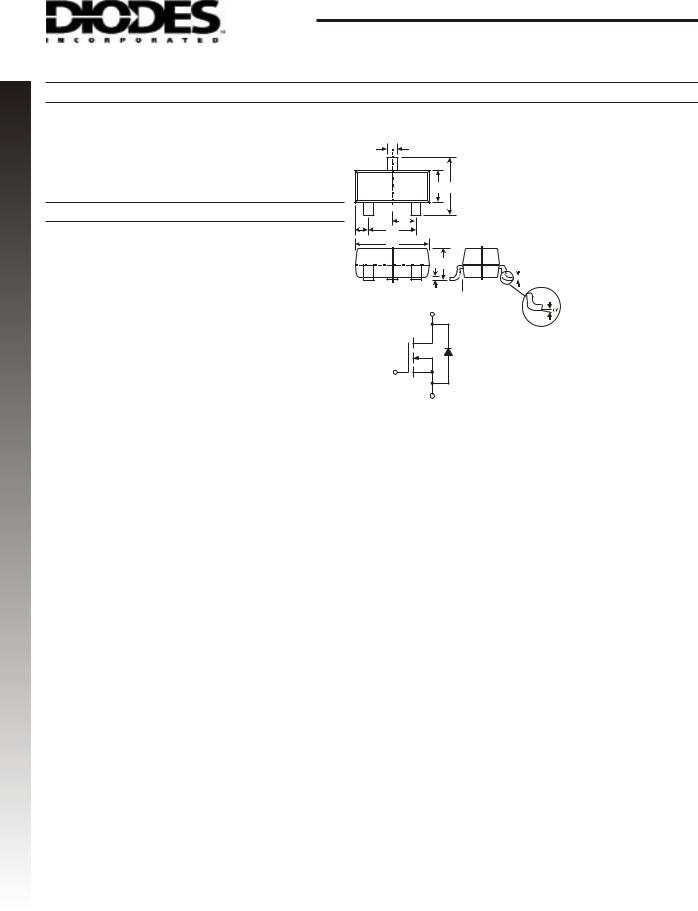
BSS123
N-CHANNEL ENHANCEMENT MODE FIELD EFFECT
TRANSISTOR
Features
Low Gate Threshold Voltage
Low Input Capacitance
Fast Switching Speed
Low Input/Output Leakage
High Drain-Source Voltage Rating
Mechanical Data
Case: SOT-23, Molded Plastic
Case material - UL Flammability Rating 94V-0
Moisture sensitivity: Level 1 per J-STD-020A
Terminals: Solderable per MIL-STD-202, Method 208
Terminal Connections: See Diagram
Marking: K23 (See Page 3)
Ordering & Date Code Information: See Page 3
Weight: 0.008 grams (approx.)
|
|
A |
|
|
D |
|
|
|
|
B |
C |
G |
TOP VIEW |
S |
|
E |
D |
|
|
G |
|
|
|
|
|
|
|
|
H |
|
|
K
J
 L
L
Drain
Gate
|
|
|
|
|
SOT-23 |
|
|
|
|
|
|
|
|
|
|
|
|
|
|
Dim |
Min |
Max |
|
|
|
|
|
|
|
|
|
|
|
|
|
A |
0.37 |
0.51 |
|
|
|
|
|
|
|
|
|
|
|
|
|
B |
1.20 |
1.40 |
|
|
|
|
|
|
|
|
|
|
|
|
|
C |
2.30 |
2.50 |
|
|
|
|
|
|
|
|
|
|
|
|
|
D |
0.89 |
1.03 |
|
|
|
|
|
|
|
|
|
|
|
|
|
E |
0.45 |
0.60 |
|
|
|
|
|
|
|
|
|
|
|
|
|
G |
1.78 |
2.05 |
|
|
|
|
|
|
|
|
|
M |
H |
2.80 |
3.00 |
||||
|
|
|
|||||
J |
0.013 |
0.10 |
|||||
|
|
|
|
||||
|
|
|
|
||||
|
|
|
|
||||
|
|
|
|
|
|
|
|
|
|
|
|
K |
0.903 |
1.10 |
|
|
|
|
|
||||
|
|
|
|
||||
|
|
|
|
|
|
|
|
|
|
|
|
L |
0.45 |
0.61 |
|
|
|
|
|
|
|
|
|
|
|
|
|
M |
0.085 |
0.180 |
|
|
|
|
|
|
|
|
|
|
|
|
|
|
0 |
8 |
|
|
|
|
|
|
|
|
|
|
|
|
|
All Dimensions in mm |
|||
|
|
|
|
|
|
|
|
|
|
|
|
|
|
|
|
|
|
|
Source |
|
|
|
|
|
|
|
|
Maximum Ratings |
@ TA = 25 C unless otherwise specified |
|
|
|
|
|
|
|
|
|
|
Characteristic |
Symbol |
|
BSS123 |
Units |
|
|
|
|
|
|
|
Drain-Source Voltage |
|
VDSS |
|
100 |
V |
|
|
|
|
|
|
Drain-Gate Voltage RGS 20K |
VDGR |
|
100 |
V |
|
Gate-Source Voltage |
Continuous |
VGSS |
|
20 |
V |
|
|
|
|
|
|
Drain Current (Note 1) |
Continuous |
ID |
|
170 |
mA |
|
Pulsed |
IDM |
|
680 |
|
|
|
|
|||
|
|
|
|
|
|
Total Power Dissipation (Note 1) |
Pd |
|
300 |
mW |
|
Thermal Resistance, Junction to Ambient (Note 1) |
R JA |
|
417 |
C/W |
|
|
|
|
|
|
|
Operating and Storage Temperature Range |
Tj, TSTG |
|
-55 to +150 |
C |
|
|
|
|
|
|
|
|
|
|
|
|
|
Note: 1. Part mounted on FR-4 board with recommended pad layout, which can be found on our website at http://www.diodes.com/datasheets/ap02001.pdf.
DS30366 Rev. 3 - 2 |
10 |
BSS123 |
|
www.diodes.com |
|
Integrated |
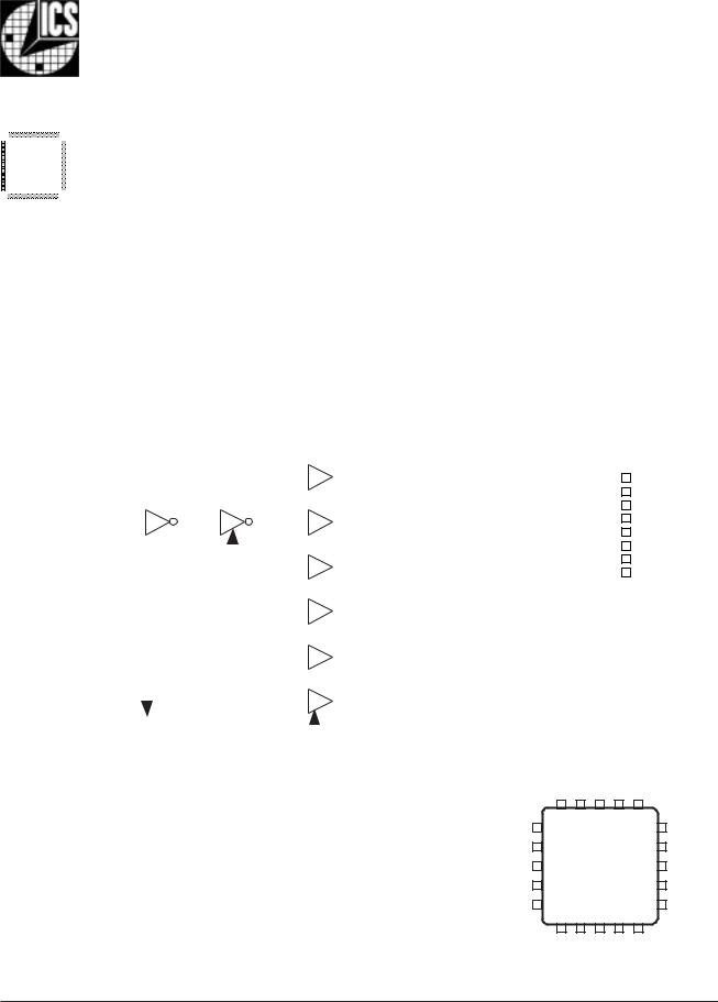
ICS83905 |
Circuit |
LOW SKEW, 1:6 CRYSTAL INTERFACE-TO- |
Systems, Inc. |
LVCMOS / LVTTL FANOUT BUFFER |
|
GENERAL DESCRIPTION
|
The ICS83905 is a low skew, 1-to-6 LVCMOS / |
|
ICS |
||
LVTTL Fanout Buffer and a member of the |
||
HiPerClockS™ |
HiPerClockS™family of High Performance Clock |
|
|
||
|
Solutions from ICS. The ICS83905 single ended |
|
|
clock input accepts LVCMOS or LVTTL input lev- |
els. The low impedance LVCMOS/LVTTL outputs are designed to drive 50Ω series or parallel terminated transmission lines. The effective fanout can be increased from 6 to 12 by utilizing the ability of the outputs to drive two series terminated lines.
The ICS83905 is characterized at full 3.3V, 2.5V, and 1.8V, mixed 3.3V/2.5V, 3.3V/1.8V and 2.5V/1.8V output operating supply mode. Guaranteed output and part-to-part skew characteristics along with the 1.8V output capabilities makes the ICS83905 ideal for high performance, single ended applications that also require a limited output voltage.
FEATURES
•6 LVCMOS / LVTTL outputs
•Crystal oscillator interface
•Output frequency range: 10MHz to 50MHz
•Crystal input frequency range: 10MHz to 50MHz
•Output skew: 10ps (typical)
•5V tolerant enable inputs
•Synchronous output enables
•Operating supply modes: Full 3.3V, 2.5V and 1.8V, mixed 3.3Vcore/2.5V or1.8V operating supply, and mixed 2.5V core/1.8V operating supply
•0°C to 70°C ambient operating temperature
•Lead-Free package fully RoHS compliant
•Pin compatible to MPC905
•Industrial version available upon request
BLOCK DIAGRAM |
PIN ASSIGNMENT |
|
|
|
|
|
|
|
|
|
|
|||||||||||||
|
|
|
|
|
|
|
|
|
|
|
|
|
BCLK0 |
|
|
|
|
|
|
|
|
|
|
|
|
|
|
|
|
|
|
|
|
|
|
|
|
|
XTAL_OUT |
|
1 |
|
16 |
|
|
XTAL_IN |
|||
|
|
|
|
|
|
|
|
|
|
|
|
|
|
ENABLE 2 |
|
2 |
|
15 |
|
|
ENABLE 1 |
|||
|
|
|
|
|
|
|
|
|
|
|
|
|
|
|
|
|
||||||||
|
|
|
|
|
|
|
|
|
|
|
|
|
|
|
GND |
|
3 |
|
14 |
|
|
BCLK5 |
|
|
|
|
|
|
|
|
|
|
|
|
|
|
|
|
|
|
|
|
|
||||||
|
|
|
|
|
|
|
|
|
|
|
|
|
BCLK1 |
|
BCLK0 |
|
4 |
|
13 |
|
|
VDDO |
|
|
|
|
|
|
|
|
|
|
|
|
|
|
|
|
|
|
|
|
|||||||
|
XTAL_IN |
|
|
|
|
|
|
|
|
|
|
|
VDDo |
|
|
5 |
|
12 |
|
|
BCLK4 |
|
||
|
|
|
|
|
|
|
|
|
|
|
|
|
|
|
BCLK1 |
|
6 |
|
11 |
|
|
GND |
|
|
|
|
|
|
|
|
|
|
|
|
|
|
|
BCLK2 |
|
GND |
|
7 |
|
10 |
|
|
BCLK3 |
|
|
|
XTAL_OUT |
|
|
|
|
|
|
|
|
|
|
|
|
|
||||||||||
|
|
|
|
|
|
|
|
|
|
|
BCLK2 |
|
8 |
|
9 |
|
|
VDD |
|
|||||
|
|
|
|
|
|
|
|
|
|
|
|
|
|
|
|
|||||||||
|
|
|
|
|
|
|
|
|
|
|
|
|
|
|
|
|
|
|
|
|
||||
|
|
|
|
|
|
|
|
|
|
|
|
|
BCLK3 |
|
|
|
ICS83905 |
|
||||||
|
|
|
|
|
|
|
|
|
|
|
|
|
|
16-Lead SOIC |
|
|||||||||
|
|
|
|
|
|
|
|
|
|
|
|
|
|
|
||||||||||
|
|
|
|
|
|
|
|
|
|
|
|
|
|
3.9mm x 9.9mm x 1.38mm body package |
||||||||||
|
|
|
|
|
|
|
|
|
|
|
|
|
|
|
|
|
M Pacakge |
|
|
|||||
|
|
|
|
|
|
|
|
|
|
|
|
|
BCLK4 |
|
|
|
|
Top View |
|
|
|
|||
|
|
|
|
|
|
|
|
|
|
|
|
|
|
|
|
|
|
|
||||||
ENABLE 1 |
|
|
|
|
|
|
|
|
|
|
|
|
|
|
|
|
ICS83905 |
|
||||||
|
|
SYNCHRONIZE |
|
|
|
|
|
|
|
|
|
|||||||||||||
|
|
|
|
|
|
|
BCLK5 |
|
16-Lead TSSOP |
|
||||||||||||||
|
|
|
|
|
|
|
|
|
|
|
|
|
|
|
||||||||||
|
|
|
|
|
|
|
|
|
|
|
|
|
|
4.4mm x 3.0mm x 0.92mm body package |
||||||||||
ENABLE 2 |
|
|
|
|
|
|
|
|
|
|
|
|
|
|
|
|
G Pacakge |
|
|
|||||
|
|
SYNCHRONIZE |
|
|
|
|
|
|
|
|
|
Top View |
|
|
|
|||||||||
|
|
|
|
|
|
|
|
|
|
|
|
|
|
|||||||||||
|
|
|
|
|
|
|
|
|
|
|
|
|
||||||||||||
|
|
|
|
|
|
|
|
|
|
|
|
|
|
|
ENABLE2 |
|
XTAL OUT |
XTAL IN |
ENABLE1 |
|
nc |
|
||
|
|
|
|
|
|
|
|
|
|
|
|
|
|
|
|
|
|
|||||||
|
|
|
|
|
|
|
|
|
|
|
|
|
|
|
20 |
19 |
18 |
17 |
16 |
|
||||
|
|
|
|
|
|
|
|
|
|
|
|
|
|
GND |
1 |
|
ICS83905 15 |
BCLK5 |
||||||
|
|
|
|
|
|
|
|
|
|
|
|
|
|
GND |
2 20-Lead VFQFN 14 |
VDDO |
||||||||
|
|
|
|
|
|
|
|
|
|
|
|
|
|
BCLK0 |
4mm x 4mm x 0.9mm |
BCLK4 |
||||||||
|
|
|
|
|
|
|
|
|
|
|
|
|
|
3 |
|
body package |
13 |
|||||||
|
|
|
|
|
|
|
|
|
|
|
|
|
|
|
|
|
|
|
||||||
|
|
|
|
|
|
|
|
|
|
|
|
|
|
VDDO |
4 |
|
K Package |
|
12 |
GND |
||||
|
|
|
|
|
|
|
|
|
|
|
|
|
|
BCLK1 |
5 |
|
|
Top View |
|
11 |
GND |
|||
|
|
|
|
|
|
|
|
|
|
|
|
|
|
|
|
|
|
|
|
|
||||
|
|
|
|
|
|
|
|
|
|
|
|
|
|
|
6 |
|
7 |
8 |
9 |
|
10 |
|
||
|
|
|
|
|
|
|
|
|
|
|
|
|
|
|
GND |
|
GND |
BCLK2 |
VDD |
|
BCLK3 |
|
||
The Preliminary Information presented herein represents a product in prototyping or pre-production. The noted characteristics are based on initial product characterization. Integrated Circuit Systems, Incorporated (ICS) reserves the right to change any circuitry or specifications without notice.
83905AM |
http://www.icst.com/products/hiperclocks.html |
REV. A JANUARY 20, 2005 |
11


 ®
®
OPA134 |
OPA2134 |
OPA4134 |
|
||
|
|
|
OPA134 |
OPA2134 |
OPA4134 |
|
||
|
|
OPA134
OPA2134
OPA4134
TM High Performance
AUDIO OPERATIONAL AMPLIFIERS
FEATURES
●SUPERIOR SOUND QUALITY
●ULTRA LOW DISTORTION: 0.00008%
●LOW NOISE: 8nV/√Hz
●TRUE FET-INPUT: IB = 5pA
●HIGH SPEED:
SLEW RATE: 20V/µs
BANDWIDTH: 8MHz
●HIGH OPEN-LOOP GAIN: 120dB (600Ω)
●WIDE SUPPLY RANGE: ±2.5V to ±18V
●SINGLE, DUAL, AND QUAD VERSIONS
APPLICATIONS
●PROFESSIONAL AUDIO AND MUSIC
●LINE DRIVERS
●LINE RECEIVERS
●MULTIMEDIA AUDIO
●ACTIVE FILTERS
●PREAMPLIFIERS
●INTEGRATORS
●CROSSOVER NETWORKS
DESCRIPTION
The OPA134 series are ultra-low distortion, low noise operational amplifiers fully specified for audio applications. A true FET input stage was incorporated to provide superior sound quality and speed for exceptional audio performance. This in combination with high output drive capability and excellent dc performance allows use in a wide variety of demanding applications. In addition, the OPA134’s wide output swing, to within 1V of the rails, allows increased headroom making it ideal for use in any audio circuit.
OPA134 op amps are easy to use and free from phase inversion and overload problems often found in common FET-input op amps. They can be operated from
±2.5V to ±18V power supplies. Input cascode circuitry provides excellent common-mode rejection and maintains low input bias current over its wide input voltage range, minimizing distortion. OPA134 series op amps are unity-gain stable and provide excellent dynamic behavior over a wide range of load conditions, including high load capacitance. The dual and quad versions feature completely independent circuitry for lowest crosstalk and freedom from interaction, even when overdriven or overloaded.
Single and dual versions are available in 8-pin DIP and SO-8 surface-mount packages in standard configurations. The quad is available in 14-pin DIP and SO-14 surface mount packages. All are specified for –40°C to +85°C operation. A SPICE macromodel is available for design analysis.
|
|
OPA134 |
|
|
Offset Trim |
1 |
8 |
Offset Trim |
|
–In |
2 |
7 |
V+ |
|
+In |
3 |
6 |
Output |
|
V– |
4 |
5 |
NC |
Out A |
|
|
8-Pin DIP, SO-8 |
|
–In A |
|
|
|
|
|
|
|
|
|
+In A |
V–
|
|
|
|
|
|
|
|
|
|
|
|
|
Out A |
|
|
|
|
|
|
|
|
|
|
|
|
|
–In A |
|
|
OPA2134 |
|
|
+In A |
||||||||
|
|
|
|
|
|
|
|
|
|
|
|
|
|
|
|
|
|
|
|
|
|
|
|
|
|
V+ |
V+ |
1 |
|
|
|
|
|
|
|
|
|
|
8 |
||
|
|
|
|
|
|
|
|
|
|
|
|||
|
|
|
|
|
|
|
|
|
|
|
|
|
+In B |
|
|
|
|
|
|
|
|
|
|
|
|
|
|
2 |
|
A |
7 |
Out B |
|||||||||
|
|
|
|
|
|
|
|
|
|
|
|
|
–In B |
|
|
|
|
|
|
|
|
|
|
|
|
|
|
|
|
|
|
|
|
|
|
|
|
|
|
|
|
3 |
|
|
|
|
|
|
|
B |
6 |
–In B |
|||
|
|
|
|
|
|
|
|
|
|
|
|
+In B |
Out B |
|
|
|
|
|
|
|
|
|
|
|
|
||
4 |
|
|
|
|
|
|
|
|
|
|
5 |
||
|
|
|
|
|
|
|
|
|
|
|
|||
|
|
|
|
|
|
|
|
|
|
|
|
|
|
OPA4134
1 |
2 |
A |
3 |
4
5 |
B |
6 |
7 |
14 |
Out D |
13 |
–In D |
D |
|
12 |
+In D |
11 |
V– |
10 |
+In C |
C |
|
9 |
–In C |
8 |
Out C |
8-Pin DIP, SO-8 |
14-Pin DIP |
|
SO-14 |
||
|
International Airport Industrial Park • Mailing Address: PO Box 11400, Tucson, AZ 85734 • Street Address: 6730 S. Tucson Blvd., Tucson, AZ 85706 • Tel: (520) 746-1111 • Twx: 910-952-1111 Internet: http://www.burr-brown.com/ • FAXLine: (800) 548-6133 (US/Canada Only) • Cable: BBRCORP • Telex: 066-6491 • FAX: (520) 889-1510 • Immediate Product Info: (800) 548-6132
© 1996 Burr-Brown Corporation |
PDS-1339C |
Printed in U.S.A. December, 1997 |
12
PCA9554A
REMOTE 8-BIT I2C AND SMBus I/O EXPANDER
WITH INTERRUPT OUTPUT AND CONFIGURATION REGISTERS
www.ti.com |
SCPS127A–SEPTEMBER 2006–REVISED FEBRUARY 2007 |
|
FEATURES
•I2C to Parallel Port Expander
•Open-Drain Active-Low Interrupt Output
•Operating Power-Supply Voltage Range of 2.3 V to 5.5 V
•5-V Tolerant I/Os
•400-kHz Fast I2C Bus
•Three Hardware Address Pins Allow up to Eight Devices on the I2C/SMBus
•Input/Output Configuration Register
•Polarity Inversion Register
•Internal Power-On Reset
•Power-Up With All Channels Configured as Inputs
•No Glitch on Power-Up
•Latched Outputs With High-Current Drive Maximum Capability for Directly Driving LEDs
•Latch-Up Performance Exceeds 100 mA Per JESD 78, Class II
•ESD Protection Exceeds JESD 22
–2000-V Human-Body Model (A114-A)
–200-V Machine Model (A115-A)
–1000-V Charged-Device Model (C101)
DB, DBQ, DGV, DW, OR PW PACKAGE (TOP VIEW)
A0 |
|
1 |
16 |
|
|
VCC |
|
|
|
|
|||||
|
|
|
|
|
|||
A1 |
|
2 |
15 |
|
|
SDA |
|
|
|
|
|
|
|
||
A2 |
|
3 |
14 |
|
|
SCL |
|
P0 |
|
4 |
13 |
|
|
|
|
|
|
|
INT |
|
|||
P1 |
|
5 |
12 |
|
|
P7 |
|
P2 |
|
6 |
11 |
|
|
P6 |
|
|
|
|
|||||
P3 |
|
7 |
10 |
|
|
P5 |
|
|
|
|
|||||
|
|
|
|
|
|
||
GND |
|
8 |
9 |
|
|
P4 |
|
|
|
|
|
|
|
|
|
RGV PACKAGE
(TOP VIEW)
|
A1 |
A0 |
V |
SDA |
|
|
|
|
CC |
|
|
|
16 |
15 |
14 |
13 |
|
A2 |
1 |
|
|
12 |
SCL |
P0 |
2 |
|
|
11 |
INT |
P1 |
3 |
|
|
10 |
P7 |
P2 |
4 |
|
|
9 |
P6 |
|
5 |
6 |
7 |
8 |
|
|
P3 |
GND |
P4 |
P5 |
|
RGT PACKAGE
(TOP VIEW)
|
A1 A0 |
V |
SDA |
|
|
|
|
|
CC |
|
|
A2 |
16 15 14 |
13 |
SCL |
||
1 |
|
|
12 |
||
P0 |
2 |
|
|
11 |
INT |
P1 |
3 |
|
|
10 |
P7 |
P2 |
4 |
|
|
9 |
P6 |
|
5 |
6 |
7 |
8 |
|
|
P3 |
GND |
P4 |
P5 |
|
DESCRIPTION/ORDERING INFORMATION
This 8-bit I/O expander for the two-line bidirectional bus (I2C) is designed for 2.3-V to 5.5-V VCC operation. It provides general-purpose remote I/O expansion for most microcontroller families via the I2C interface [serial clock (SCL), serial data (SDA)].
The PCA9554A consists of one 8-bit Configuration (input or output selection), Input, Output, and Polarity Inversion (active high or active low) registers. At power-on, the I/Os are configured as inputs with a weak pull up to VCC. However, the system master can enable the I/Os as either inputs or outputs by writing to the I/O configuration bits. The data for each input or output is kept in the corresponding Input or Output register. The polarity of the Input Port register can be inverted with the Polarity Inversion register. All registers can be read by the system master.
The system master can reset the PCA9554A in the event of a timeout or other improper operation by utilizing the power-on reset feature which puts the registers in their default state and initializes the I2C/SMBus state machine.
The PCA9554A open-drain interrupt (INT) output is activated when any input state differs from its corresponding Input Port register state and is used to indicate to the system master that an input state has changed.
INT can be connected to the interrupt input of a microcontroller. By sending an interrupt signal on this line, the remote I/O can inform the microcontroller if there is incoming data on its ports without having to communicate via the I2C bus. Thus, the PCA9554A can remain a simple slave device.
The device's outputs (latched) have high-current drive capability for directly driving LEDs and low current consumption.
Please be aware that an important notice concerning availability, standard warranty, and use in critical applications of Texas Instruments semiconductor products and disclaimers thereto appears at the end of this data sheet.
UNLESS OTHERWISE NOTED this |
document |
contains |
Copyright © 2006–2007, Texas Instruments Incorporated |
PRODUCTION DATA information current as of publication date. |
|
||
Products conform to specifications per |
the terms |
of Texas |
|
Instruments standard warranty. Production processing does not |
|
||
necessarily include testing of all parameters. |
|
|
|
13

Burr Brown Products from Texas Instruments

 SRC4392
SRC4392
SBFS029B–DECEMBER 2005–REVISED APRIL 2006
Two-Channel, Asynchronous Sample Rate Converter with Integrated Digital Audio Interface Receiver and Transmitter
FEATURES
•Two-Channel Asynchronous Sample Rate Converter (SRC)
–Dynamic Range with –60dB Input (A-Weighted): 144dB typical
–Total Harmonic Distortion and Noise (THD+N) with Full-Scale Input: –140dB typical
–Supports Audio Input and Output Data Word Lengths Up to 24 Bits
–Supports Input and Output Sampling Frequencies Up to 216kHz
–Automatic Detection of the Input-to-Output Sampling Ratio
–Wide Input-to-Output Conversion Range: 16:1 to 1:16 Continuous
–Excellent Jitter Attenuation Characteristics
–Digital De-Emphasis Filtering for 32kHz, 44.1kHz, and 48kHz Input Sampling Rates
–Digital Output Attenuation and Mute Functions
–Output Word Length Reduction
–Status Registers and Interrupt Generation for Sampling Ratio and Ready Flags
•Digital Audio Interface Transmitter (DIT)
–Supports Sampling Rates Up to 216kHz
–Includes Differential Line Driver and CMOS Buffered Outputs
–Block-Sized Data Buffers for Both Channel Status and User Data
–Status Registers and Interrupt Generation for Flag and Error Conditions
•User-Selectable Serial Host Interface: SPI or Philips I2C™
–Provides Access to On-Chip Registers and Data Buffers
•Digital Audio Interface Receiver (DIR)
–PLL Lock Range Includes Sampling Rates from 20kHz to 216kHz
–Includes Four Differential Input Line Receivers and an Input Multiplexer
–Bypass Multiplexer Routes Line Receiver Outputs to Line Driver and Buffer Outputs
–Block-Sized Data Buffers for Both Channel Status and User Data
–Automatic Detection of Non-PCM Audio Streams (DTS CD/LD and IEC 61937 formats)
–Audio CD Q-Channel Sub-Code Decoding and Data Buffer
–Status Registers and Interrupt Generation for Flag and Error Conditions
–Low Jitter Recovered Clock Output
•Two Audio Serial Ports (Ports A and B)
–Synchronous Serial Interface to External Signal Processors, Data Converters, and Logic
–Slave or Master Mode Operation with Sampling Rates up to 216kHz
–Supports Left-Justified, Right-Justified, and Philips I2S™ Data Formats
–Supports Audio Data Word Lengths Up to 24 Bits
•Four General-Purpose Digital Outputs
–Multifunction Programmable Via Control Registers
•Extensive Power-Down Support
–Functional Blocks May Be Disabled Individually When Not In Use
•Operates From +1.8V Core and +3.3V I/O Power Supplies
•Small TQFP-48 Package, Compatible with the SRC4382 and DIX4192
Please be aware that an important notice concerning availability, standard warranty, and use in critical applications of Texas Instruments semiconductor products and disclaimers thereto appears at the end of this data sheet.
Dolby is a registered trademark of Dolby Laboratories.
I2C, I2S are trademarks of Koninklijke Philips Electronics N.V. All other trademarks are the property of their respective owners.
PRODUCTION DATA information is current as of publication date. |
Copyright © 2005–2006, Texas Instruments Incorporated |
Products conform to specifications per the terms of the Texas |
|
Instruments standard warranty. Production processing does not |
|
necessarily include testing of all parameters. |
|
14
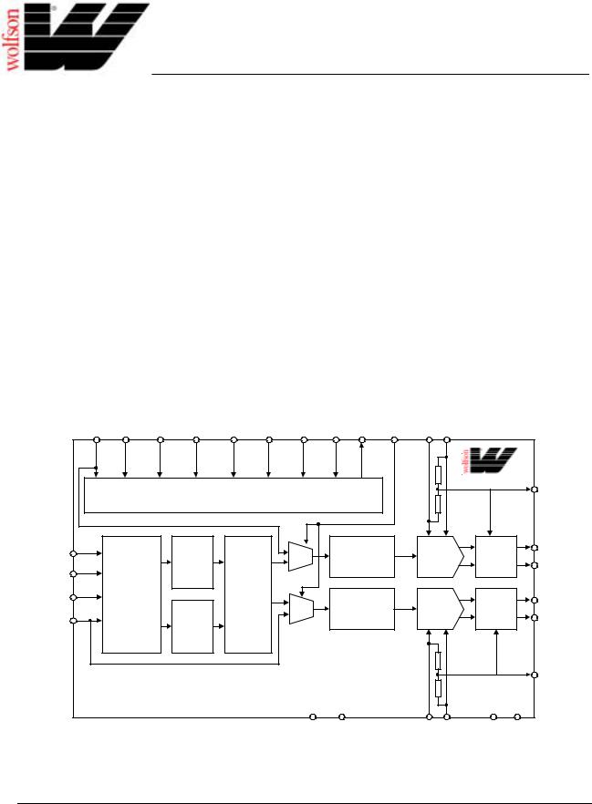
WM8740
24-bit, High Performance 192kHz Stereo DAC
Advanced Information, July 2000, Rev 1.7
DESCRIPTION
The WM8740 is a very high performance stereo DAC designed for audio applications such as CD, DVD, home theatre systems, set top boxes and digital TV. The WM8740 supports data input word lengths from 16 to 24-bits and sampling rates up to 192kHz. The WM8740 consists of a serial interface port, digital interpolation filter, multi-bit sigma delta modulator and stereo DAC in a small 28-pin SSOP package. The WM8740 also includes a digitally controllable mute and attenuator function on each channel.
The internal digital filter has two selectable roll-off characteristics. A sharp or slow roll-off can be selected dependent on application requirements. Additionally, the internal digital filter can be by-passed and the WM8740 used with an external digital filter.
The WM8740 supports two connection schemes for audio DAC control. The SPI-compatible serial control port provides access to a wide range of features including onchip mute, attenuation and phase reversal. A hardware controllable interface is also available.
FEATURES
•120dB SNR (‘A’ weighted mono @48kHz), THD+N: -104dB
@FS
•117dB SNR (‘A’ weighted stereo @48kHz), THD+N: -104dB
@FS
•Sampling frequency: 8kHz to 192kHz
•Selectable digital filter roll-off
•Optional interface to industry standard external filters
•Differential mono mode needing no glue logic
•Input data word: 16 to 24-bit
•Hardware or SPI compatible serial port control modes:
•Hardware mode: mute, de-emphasis, audio format control
•Serial mode: mute, de-emphasis, attenuation (256 steps), phase reversal
•Fully differential voltage outputs
APPLICATIONS
•CD, DVD audio
•Home theatre systems
•Professional audio systems
BLOCK DIAGRAM
MODE ML/I2S MC/DM1 MD/DM0 DIFFHW MUTEB CSBIWO RSTB ZERO MODE8X AGNDR AVDDR |
|
||||||||||||
(24) |
(28) |
(27) |
(26) |
(6) |
(25) |
(23) |
(22) |
(21) |
(4) |
(10) |
(9) |
|
|
|
|
|
|
|
|
|
|
|
|
|
|
WM8740 |
(11) VMIDR |
|
|
|
CONTROL INTERFACE |
|
|
|
|
|
|
|
|||
|
|
|
|
|
|
|
|
|
|
|
|||
SCLK (5) |
|
|
|
|
|
|
|
SIGMA |
|
RIGHT |
LOW |
(12) VOUTRP |
|
|
|
MUTE/ |
|
|
MUX |
|
DELTA |
|
PASS |
|
|||
|
|
|
|
|
|
|
DAC |
|
|
||||
|
|
|
ATTEN |
|
|
|
MODULATOR |
|
|
FILTER |
(13) VOUTRN |
||
BCKIN (3) |
|
|
|
|
|
|
|
|
|||||
|
|
|
|
|
|
|
|
|
|
|
|
|
|
LRCIN (1) |
SERIAL |
|
|
DIGITAL |
|
|
SIGMA |
|
|
|
LOW |
|
|
INTERFACE |
|
FILTERS |
MUX |
|
|
LEFT |
|
(17) VOUTLP |
|||||
|
|
|
|
|
|
|
DELTA |
|
|
PASS |
|
||
|
|
|
|
|
|
|
|
DAC |
|
(16) VOUTLN |
|||
DIN (2) |
|
|
MUTE/ |
|
|
|
MODULATOR |
|
|
FILTER |
|||
|
|
|
|
|
|
|
|
||||||
|
|
|
|
|
|
|
|
|
|
|
|
||
|
|
|
ATTEN |
|
|
|
|
|
|
|
|
|
|
|
|
|
|
|
|
|
|
|
|
|
|
|
(18) VMIDL |
(15) |
(8) |
(20) (19) |
(14) |
(7) |
AVDD DVDD |
AVDDL AGNDL |
AGND |
DGND |
|
WOLFSON MICROELECTRONICS LTD |
Advanced Information data sheets contain |
Lutton Court, Bernard Terrace, Edinburgh, EH8 9NX, UK |
preliminary data on new products in the |
Tel: +44 (0) 131 667 9386 |
preproduction phase of development. |
Fax: +44 (0) 131 667 5176 |
Supplementary data will be published at a |
Email: sales@wolfson.co.uk |
later date. |
http://www.wolfson.co.uk |
2000 Wolfson Microelectronics Ltd. |
15
PIC18F66J10 FAMILY
|
Program Memory |
|
|
|
|
|
MSSP |
|
EUSART |
Comparators |
Timers bit-8/16 |
BusExternal |
||
|
|
|
|
|
|
|
|
|
|
|
||||
|
|
|
SRAM Data |
|
10-bit |
CCP/ |
|
|
|
|
|
|
|
|
|
|
|
|
|
|
|
|
|
|
|
|
|||
Device |
Flash |
# Single-Word |
Memory |
I/O |
ECCP |
|
|
|
Master |
|
|
|
|
|
A/D (ch) |
|
SPI™ |
|
|
|
|
|
|||||||
|
(bytes) |
|
(PWM) |
|
|
|
|
|
|
|||||
|
(bytes) |
Instructions |
|
|
|
|
|
I2C™ |
|
|
|
|
||
|
|
|
|
|
|
|
|
|
|
|
|
|
|
|
PIC18F65J10 |
32K |
16384 |
2048 |
50 |
11 |
2/3 |
2 |
Y |
|
Y |
2 |
2 |
2/3 |
N |
PIC18F65J15 |
48K |
24576 |
2048 |
50 |
11 |
2/3 |
2 |
Y |
|
Y |
2 |
2 |
2/3 |
N |
|
|
|
|
|
|
|
|
|
|
|
|
|
|
|
PIC18F66J10 |
64K |
32768 |
2048 |
50 |
11 |
2/3 |
2 |
Y |
|
Y |
2 |
2 |
2/3 |
N |
|
|
|
|
|
|
|
|
|
|
|
|
|
|
|
PIC18F66J15 |
96K |
49152 |
3936 |
50 |
11 |
2/3 |
2 |
Y |
|
Y |
2 |
2 |
2/3 |
N |
|
|
|
|
|
|
|
|
|
|
|
|
|
|
|
PIC18F67J10 |
128K |
65536 |
3936 |
50 |
11 |
2/3 |
2 |
Y |
|
Y |
2 |
2 |
2/3 |
N |
|
|
|
|
|
|
|
|
|
|
|
|
|
|
|
PIC18F85J10 |
32K |
16384 |
2048 |
66 |
15 |
2/3 |
2 |
Y |
|
Y |
2 |
2 |
2/3 |
Y |
PIC18F85J15 |
48K |
24576 |
2048 |
66 |
15 |
2/3 |
2 |
Y |
|
Y |
2 |
2 |
2/3 |
Y |
|
|
|
|
|
|
|
|
|
|
|
|
|
|
|
PIC18F86J10 |
64K |
32768 |
2048 |
66 |
15 |
2/3 |
2 |
Y |
|
Y |
2 |
2 |
2/3 |
Y |
PIC18F86J15 |
96K |
49152 |
3936 |
66 |
15 |
2/3 |
2 |
Y |
|
Y |
2 |
2 |
2/3 |
Y |
|
|
|
|
|
|
|
|
|
|
|
|
|
|
|
PIC18F87J10 |
128K |
65536 |
3936 |
66 |
15 |
2/3 |
2 |
Y |
|
Y |
2 |
2 |
2/3 |
Y |
|
|
|
|
|
|
|
|
|
|
|
|
|
|
|
Pin Diagrams
64-Pin TQFP |
|
RE2/CS/P2B |
RE3/P3C |
RE4/P3B |
RE5/P1C |
RE6/P1B |
RE7/ECCP2 |
RD0/PSP0 |
VDD |
VSS |
RD1/PSP1 |
RD2/PSP2 |
RD3/PSP3 |
RD4/PSP4/SDO2 |
RD5/PSP5/SDI2/SDA2 |
RD6/PSP6/SCK2/SCL2 |
RD7/PSP7/SS2 |
||||||||||||||||||||||||
|
|
|
|
|
|
|
|
|
|
|
|
|
|
|
|
|
|
|
(1) |
|
|
|
|
|
|
|
|
|
|
|
|
|
|
|
|
|
|
|
|
|
|
|
|
|
|
|
|
|
|
|
|
|
|
|
|
|
|
|
|
|
/P2A |
|
|
|
|
|
|
|
|
|
|
|
|
|
|
|
|
|
|
|
|
|
|
|
|
|
|
|
|
|
|
|
|
|
|
|
|
|
|
|
|
|
|
|
|
|
|
|
|
|
|
|
|
|
|
|
|
|
|
|
|
|
|
||
|
|
|
|
|
|
|
|
|
|
|
|
|
|
|
|
|
|
|
(1) |
|
|
|
|
|
|
|
|
|
|
|
|
|
|
|
|
|
|
|
|
|
|
|
|
|
|
|
|
|
|
|
|
|
|
|
|
|
|
|
|
|
|
|
|
|
|
|
|
|
|
|
|
|
|
|
|
|
|
|
|
|
|
|
|
|
|
|
|
|
|
|
|
|
|
|
|
|
|
|
|
|
|
|
|
|
|
|
|
|
|
|
|
|
|
|
|
|
|
|
|
|
|
|
|
|
|
|
|
|
|
|
|
|
|
|
|
|
|
|
|
|
|
|
|
|
|
|
|
|
|
|
|
|
|
|
|
|
|
|
|
|
|
|
|
|
|
|
|
|
|
|
|
|
|
|
|
|
|
|
|
|
|
|
|
|
|
|
|
|
|
|
|
|
|
|
|
|
|
|
|
|
|
|
|
|
|
|
|
|
|
|
|
|
|
|
|
|
|
|
|
|
|
|
|
|
|
|
|
|
|
|
|
|
|
|
|
|
|
|
|
|
|
|
|
|
|
|
|
|
|
|
|
|
|
|
|
|
|
|
|
64 |
63 62 |
61 |
60 |
59 |
58 |
57 |
56 55 |
54 |
53 |
52 51 |
50 |
49 |
|||||||||||||||||||||
|
|
|
|
|
|
|
|
||||||||||||||||||||||||||||||||||
|
|
|
|
|
|
1 |
|
|
|
|
|
|
|
|
|
|
|
|
|
|
|
|
|
|
|
|
|
|
|
|
|
|
|
|
|
|
48 |
||||
RE1/ |
WR |
/P2C |
|
|
|
|
|
|
|
|
|
|
|
|
|
|
|
|
|
|
|
|
|
|
|
|
|
|
|
|
|
|
|
||||||||
|
|
|
|
|
|
|
|
|
|
|
|
|
|
|
|
|
|
|
|
|
|
|
|
|
|
|
|
|
|
||||||||||||
|
|
|
|
|
|
|
|
|
|
|
|
|
|
|
|
|
|
|
|
|
|
|
|
|
|
|
|
|
|
||||||||||||
RE0/RD/P2D |
|
2 |
|
|
|
|
|
|
|
|
|
|
|
|
|
|
|
|
|
|
|
|
|
|
|
|
|
|
|
|
|
|
47 |
||||||||
|
|
|
|
|
|
|
|
|
|
|
|
|
|
|
|
|
|
|
|
|
|
|
|
|
|
|
|
|
|
||||||||||||
RG0/ECCP3/P3A |
|
3 |
|
|
|
|
|
|
|
|
|
|
|
|
|
|
|
|
|
|
|
|
|
|
|
|
|
|
|
|
|
|
46 |
||||||||
|
|
|
|
|
|
|
|
|
|
|
|
|
|
|
|
|
|
|
|
|
|
|
|
|
|
|
|
|
|
||||||||||||
RG1/TX2/CK2 |
|
4 |
|
|
|
|
|
|
|
|
|
|
|
|
|
|
|
|
|
|
|
|
|
|
|
|
|
|
|
|
|
|
45 |
||||||||
|
|
|
|
|
|
|
|
|
|
|
|
|
|
|
|
|
|
|
|
|
|
|
|
|
|
|
|
|
|
||||||||||||
RG2/RX2/DT2 |
|
5 |
|
|
|
|
|
|
|
|
|
|
|
|
|
|
|
|
|
|
|
|
|
|
|
|
|
|
|
|
|
|
44 |
||||||||
|
|
|
|
|
|
|
|
|
|
|
|
|
|
|
|
|
|
|
|
|
|
|
|
|
|
|
|
|
|
||||||||||||
|
|
|
|
|
|
|
|
|
|
|
|
|
|
|
|
|
|
|
|
|
|
|
|
|
|
|
|
|
|
||||||||||||
RG3/CCP4/P3D |
|
6 |
|
|
|
|
|
|
|
|
|
|
|
|
|
|
|
|
|
|
|
|
|
|
|
|
|
|
|
|
|
|
43 |
||||||||
|
|
|
|
|
|
|
|
|
|
|
|
|
|
|
|
|
|
|
|
|
|
|
|
|
|
|
|
|
|
||||||||||||
|
|
|
|
|
|
|
|
|
|
|
|
|
|
|
|
|
|
|
|
|
|
|
|
|
|
|
|
|
|
||||||||||||
|
|
|
|
|
7 |
|
|
|
|
|
|
|
|
|
|
|
|
|
|
|
|
|
|
|
|
|
|
|
|
|
|
|
|
|
|
42 |
|||||
|
|
MCLR |
|
|
|
|
|
|
|
|
|
|
|
|
|
|
PIC18F6XJ10 |
|
|
|
|
|
|
||||||||||||||||||
|
|
|
|
|
|
|
|
|
|
|
|
|
|
|
|
|
|||||||||||||||||||||||||
RG4/CCP5/P1D |
|
8 |
|
|
|
|
|
|
|
|
|
|
|
|
|
|
|
|
|
41 |
|||||||||||||||||||||
|
|
|
|
|
|
|
|
|
|
|
|
|
|
|
|
|
|||||||||||||||||||||||||
|
|
|
|
VSS |
|
9 |
|
|
|
|
|
|
|
|
|
|
|
PIC18F6XJ15 |
|
|
|
|
|
|
40 |
||||||||||||||||
|
|
|
|
|
|
|
|
|
|
|
|
|
|
|
|
|
|||||||||||||||||||||||||
|
|
|
|
|
|
|
|
|
|
|
|
|
|
|
|
|
|||||||||||||||||||||||||
VDDCORE/VCAP |
|
10 |
|
|
|
|
|
|
|
|
|
|
|
|
|
|
|
|
|
|
|
|
|
|
|
|
|
|
|
|
|
|
39 |
||||||||
|
|
|
|
|
|
|
|
|
|
|
|
|
|
|
|
|
|
|
|
|
|
|
|
|
|
|
|
|
|
||||||||||||
|
|
|
|
11 |
|
|
|
|
|
|
|
|
|
|
|
|
|
|
|
|
|
|
|
|
|
|
|
|
|
|
|
|
|
|
38 |
||||||
RF7/SS1 |
|
|
|
|
|
|
|
|
|
|
|
|
|
|
|
|
|
|
|
|
|
|
|
|
|
|
|
|
|
|
|
|
|||||||||
|
|
|
|
|
|
|
|
|
|
|
|
|
|
|
|
|
|
|
|
|
|
|
|
|
|
|
|
|
|
||||||||||||
RF6/AN11 |
|
12 |
|
|
|
|
|
|
|
|
|
|
|
|
|
|
|
|
|
|
|
|
|
|
|
|
|
|
|
|
|
|
37 |
||||||||
|
|
|
|
|
|
|
|
|
|
|
|
|
|
|
|
|
|
|
|
|
|
|
|
|
|
|
|
|
|
||||||||||||
RF5/AN10/CVREF |
|
13 |
|
|
|
|
|
|
|
|
|
|
|
|
|
|
|
|
|
|
|
|
|
|
|
|
|
|
|
|
|
|
36 |
||||||||
|
|
|
|
|
|
|
|
|
|
|
|
|
|
|
|
|
|
|
|
|
|
|
|
|
|
|
|
|
|
||||||||||||
RF4/AN9 |
|
14 |
|
|
|
|
|
|
|
|
|
|
|
|
|
|
|
|
|
|
|
|
|
|
|
|
|
|
|
|
|
|
35 |
||||||||
|
|
|
|
|
|
|
|
|
|
|
|
|
|
|
|
|
|
|
|
|
|
|
|
|
|
|
|
|
|
||||||||||||
RF3/AN8 |
|
15 |
|
|
|
|
|
|
|
|
|
|
|
|
|
|
|
|
|
|
|
|
|
|
|
|
|
|
|
|
|
|
34 |
||||||||
|
|
|
|
|
|
|
|
|
|
|
|
|
|
|
|
|
|
|
|
|
|
|
|
|
|
|
|
|
|
||||||||||||
RF2/AN7/C1OUT |
|
16 |
|
|
|
|
|
|
|
|
|
|
|
|
|
|
|
|
|
|
|
|
|
|
|
|
|
|
|
|
|
|
33 |
||||||||
|
|
|
|
|
|
|
|
|
|
|
|
|
|
|
|
|
|
|
|
|
|
|
|
|
|
|
|
|
|
||||||||||||
|
|
|
|
|
|
|
|
17 |
18 |
19 |
20 |
21 |
22 |
23 |
24 |
25 |
26 |
27 |
28 |
29 |
30 31 |
32 |
|
||||||||||||||||||
|
|
|
|
|
|
|
|
|
|
|
|
|
|
|
|
|
|
|
|
|
|
|
|
|
|
|
|
|
|
|
|
|
|
|
|
|
|
|
|
|
|
|
|
|
|
|
|
|
|
|
|
|
|
|
|
|
|
|
|
|
|
|
|
|
|
|
|
|
|
|
|
|
|
|
|
|
|
|
|
|
|
|
|
|
|
|
|
|
|
|
|
|
RF1/AN6/C2OUT |
ENVREG |
AVDD |
AVSS |
RA3/AN3/VREF+ |
RA2/AN2/VREF- |
RA1/AN1 |
RA0/AN0 |
VSS |
VDD |
RA5/AN4 |
RA4/T0CKI |
RC1/T1OSI/ECCP2 |
RC0/T1OSO/T13CKI |
RC6/TX1/CK1 |
RC7/RX1/DT1 |
|||||||||||||||||
|
|
|
|
|
|
|
|
|
|
|
|
|
|
|
|
|
|
|
|
|
|
|
|
|
|
|
|
|
|
|
|
|
(1) |
|
|
|
|
|
|
|
|
|
|
|
|
|
|
|
|
|
|
|
|
|
|
|
|
|
|
|
|
|
|
|
|
|
|
|
|
|
|
|
|
|
/P2A |
|
|
|
|
|
|
|
|
|
|
|
|
|
|
|
|
|
|
|
|
|
|
|
|
|
|
|
|
|
|
|
|
|
|
|
|
|
|
|
|
|
(1) |
|
|
|
|
|
|
|
|
 RB0/INT0/FLT0
 RB1/INT1
 RB2/INT2
 RB3/INT3
 RB4/KBI0
 RB5/KBI1
 RB6/KBI2/PGC
VSS
 OSC2/CLKO
 OSC1/CLKI
VDD
 RB7/KBI3/PGD
 RC5/SDO1
 RC4/SDI1/SDA1
 RC3/SCK1/SCL1
  RC2/ECCP1/P1A
Note 1: The ECCP2/P2A pin placement depends on the setting of the CCP2MX configuration bit.
DS39663A-page 2 |
Advance Information |
¤ 2005 Microchip Technology Inc.
16
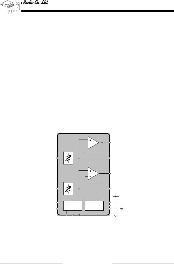
NJW1159M
2-CHANNEL ELECTRONIC VOLUME
■ GENERAL DESCRIPTION
NJW1159LV D WZR FKDQQHO HOHFWURQLF YROXPH ,& ,W LV LQFOXGHG RXWSXW EXIIHU DPSOLILHU DQG DOVR UHVLVWRU RXWSXW WHUPLQDO IRU XVLQJ H[WHUQDO DPSOLILHU WR FXVWRPL]H IRU \RXU DSSOLFDWLRQ 7KHVH IXQFWLRQV DUH FRQWUROOHG E\ WKUHH ZLUHG VHULDO GDWD $QG WKH FKLS VHOHFWRU LV DYDLODEOH IRU XVLQJ IRXU FKLSV RQ VDPH VHULDO EXV OLQH ,W¶V DYDLODEOH IRU WZR FKDQQHO VWHUHR DQG RU PXOWL FKDQQHO DXGLR YROXPH
■ PACKAGE OUTLINE
NJW1159V NJW1159M NJW1159D
■ FEATURES |
|
|
|
|
|
|
●2SHUDWLQJ 9ROWDJH |
|
|
WR 9 |
|
||
●7KUHH :LUHG 6HULDO 'DWD &RQWURO |
|
|
|
|||
●&KLS 6HOHFWRU |
|
|
DYDLODEOH IRU XVLQJ IRXU FKLSV RQ VDPH VHULDO EXV OLQH |
|||
●9ROXPH |
|
|
|
WR G% G%VWHS 087( |
||
●%L &026 7HFKQRORJ\ |
|
|
|
|
|
|
●3DFNDJH 2XWOLQH |
|
|
6623 '03 ',3 |
|||
|
|
|
|
|
|
|
■ BLOCK DIAGRAM |
|
|
|
|
|
|
|
|
|
|
|
|
|
|
|
|
|
|
|
|
|
|
|
|
|
|
% 287 / |
|
|
|
|
|
|
|
|
|
|
|
|
|
|
|
|
|
|
|
|
|
|
|
|
,1 / |
|
|
287 / |
|
|
|
|
|
||
|
|
|
|
92/ |
|
|
|
|
|
|
|
|
|
|
|
|
|
|
|
% 287 5 |
|
|
|
|
|
|
|
|
|
|
|
|
|
|
|
|
|
|
|
|
|
|
|
|
,1 5 |
|
|
287 5 |
|
|
|
|
|
||
|
|
|
|
|
|
|
|
|
|
|
92/ |
|
|
|
|
|
|
|
|
|
|
|
|
|
|
9 |
|
|
|
|
&( |
|
|
|
|
|
|
|
|
*1' |
|
|
|
|
,QWHU IDFH |
|
||
|
|
|
&( |
%LDV |
|
|
|
|
/RJLF |
|
|||
|
|
|
|
|
|
|
|
|
|
|
|
|
|
|
|
|
:LUHG |
|
|
9 |
|
|
|
|
|
||
|
|
|
|
|
|
|
|
|
&RQWURO 'DWD |
|
|
|
|
17

November 2004
LM137/LM337
3-Terminal Adjustable Negative Regulators
General Description
The LM137/LM337 are adjustable 3-terminal negative voltage regulators capable of supplying in excess of −1.5A over an output voltage range of −1.2V to −37V. These regulators are exceptionally easy to apply, requiring only 2 external resistors to set the output voltage and 1 output capacitor for frequency compensation. The circuit design has been optimized for excellent regulation and low thermal transients. Further, the LM137 series features internal current limiting, thermal shutdown and safe-area compensation, making them virtually blowout-proof against overloads.
The LM137/LM337 serve a wide variety of applications including local on-card regulation, programmable-output voltage regulation or precision current regulation. The LM137/ LM337 are ideal complements to the LM117/LM317 adjustable positive regulators.
Features
nOutput voltage adjustable from −1.2V to −37V
n1.5A output current guaranteed, −55˚C to +150˚C
nLine regulation typically 0.01%/V
nLoad regulation typically 0.3%
nExcellent thermal regulation, 0.002%/W
n77 dB ripple rejection
nExcellent rejection of thermal transients
n50 ppm/˚C temperature coefficient
nTemperature-independent current limit
nInternal thermal overload protection
nP+ Product Enhancement tested
nStandard 3-lead transistor package
nOutput is short circuit protected
LM137 Series Packages and Power Capability
|
|
Rated |
Design |
Device |
Package |
Power |
Load |
|
|
Dissipation |
Current |
|
|
|
|
LM137/337 |
TO-3 (K) |
20W |
1.5A |
|
TO-39 (H) |
2W |
0.5A |
|
|
|
|
LM337 |
TO-220 (T) |
15W |
1.5A |
|
|
|
|
LM337 |
SOT-223 |
2W |
1A |
|
(MP) |
|
|
|
|
|
|
Typical Applications |
Comparison between SOT-223 and |
Adjustable Negative Voltage Regulator |
D-Pak (TO-252) Packages |
00906731
Scale 1:1
00906701
Full output current not available at high input-output voltages
†C1 = 1 µF solid tantalum or 10 µF aluminum electrolytic required for stability
*C2 = 1 µF solid tantalum is required only if regulator is more than 4" from power-supply filter capacitor
Output capacitors in the range of 1 µF to 1000 µF of aluminum or tantalum electrolytic are commonly used to provide improved output impedance and rejection of transients
Regulators Negative Adjustable Terminal-3 LM137/LM337
© 2004 National Semiconductor Corporation |
DS009067 |
www.national.com |
18
August 1999
LM117/LM317A/LM317
3-Terminal Adjustable Regulator
General Description
The LM117 series of adjustable 3-terminal positive voltage regulators is capable of supplying in excess of 1.5A over a 1.2V to 37V output range. They are exceptionally easy to use and require only two external resistors to set the output voltage. Further, both line and load regulation are better than standard fixed regulators. Also, the LM117 is packaged in standard transistor packages which are easily mounted and handled.
In addition to higher performance than fixed regulators, the LM117 series offers full overload protection available only in IC’s. Included on the chip are current limit, thermal overload protection and safe area protection. All overload protection circuitry remains fully functional even if the adjustment terminal is disconnected.
Normally, no capacitors are needed unless the device is situated more than 6 inches from the input filter capacitors in which case an input bypass is needed. An optional output capacitor can be added to improve transient response. The adjustment terminal can be bypassed to achieve very high ripple rejection ratios which are difficult to achieve with standard 3-terminal regulators.
Besides replacing fixed regulators, the LM117 is useful in a wide variety of other applications. Since the regulator is “floating” and sees only the input-to-output differential volt-
age, supplies of several hundred volts can be regulated as long as the maximum input to output differential is not exceeded, i.e., avoid short-circuiting the output.
Also, it makes an especially simple adjustable switching regulator, a programmable output regulator, or by connecting a fixed resistor between the adjustment pin and output, the LM117 can be used as a precision current regulator. Supplies with electronic shutdown can be achieved by clamping the adjustment terminal to ground which programs the output to 1.2V where most loads draw little current.
For applications requiring greater output current, see LM150 series (3A) and LM138 series (5A) data sheets. For the negative complement, see LM137 series data sheet.
Features
nGuaranteed 1% output voltage tolerance (LM317A)
nGuaranteed max. 0.01%/V line regulation (LM317A)
nGuaranteed max. 0.3% load regulation (LM117)
nGuaranteed 1.5A output current
nAdjustable output down to 1.2V
nCurrent limit constant with temperature
nP+ Product Enhancement tested
n80 dB ripple rejection
nOutput is short-circuit protected
Typical Applications
1.2V–25V Adjustable Regulator
DS009063-1
Full output current not available at high input-output voltages *Needed if device is more than 6 inches from filter capacitors.
†Optional — improves transient response. Output capacitors in the range of 1 µF to 1000 µF of aluminum or tantalum electrolytic are commonly used to provide improved output impedance and rejection of transients.
LM117 Series Packages
Part Number |
|
Design |
Suffix |
Package |
Load |
|
|
Current |
K |
TO-3 |
1.5A |
|
|
|
H |
TO-39 |
0.5A |
|
|
|
T |
TO-220 |
1.5A |
|
|
|
E |
LCC |
0.5A |
|
|
|
S |
TO-263 |
1.5A |
|
|
|
EMP |
SOT-223 |
1A |
|
|
|
MDT |
TO-252 |
0.5A |
|
|
|
SOT-223 vs D-Pak (TO-252) Packages
DS009063-54
Scale 1:1
Regulator Adjustable Terminal-3 LM117/LM317A/LM317
© 1999 National Semiconductor Corporation |
DS009063 |
www.national.com |
19
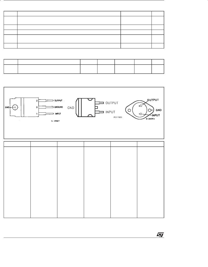
L7805CV
ABSOLUTE MAXIMUM RATINGS
Symbol |
Parameter |
Value |
Unit |
||
Vi |
DC Input Voltage (for VO = 5 to 18V) |
|
35 |
|
V |
|
(for VO = 20, 24V) |
|
40 |
|
V |
Io |
Output Current |
Internally |
limited |
|
|
Ptot |
Power Dissipation |
Internally |
limited |
|
|
Top |
Operating Junction Temperature Range (for L7800) |
-55 |
to 150 |
o C |
|
|
(for L7800C) |
0 to 150 |
o C |
||
Tst g |
Storage Temperature Range |
-65 |
to 150 |
o C |
|
THERMAL DATA
Symbol |
Parameter |
|
D2PAK |
TO-220 |
TO-220FP |
TO-3 |
Unit |
Rthjca se |
Thermal Resistance Junction-case |
Max |
3 |
3 |
5 |
4 |
oC/W |
Rthjamb |
Thermal Resistance Junction-ambient |
Max |
62.5 |
50 |
60 |
35 |
oC/W |
CONNECTION DIAGRAM AND ORDERING NUMBERS (top view)
|
TO-220 & TO-220FP |
|
D2PAK |
|
TO-3 |
Type |
TO-220 |
D2PAK (*) |
TO-220FP |
TO-3 |
Output Voltage |
L7805 |
|
|
|
L7805T |
5V |
L7805C |
L7805CV |
L7805CD2T |
L7805CP |
L7805CT |
5V |
L7852C |
L7852CV |
L7852CD2T |
L7852CP |
L7852CT |
5.2V |
L7806 |
|
|
|
L7806T |
6V |
L7806C |
L7806CV |
L7806CD2T |
L7806CP |
L7806CT |
6V |
L7808 |
|
|
|
L7808T |
8V |
L7808C |
L7808CV |
L7808CD2T |
L7808CP |
L7808CT |
8V |
L7885C |
L7885CV |
L7885CD2T |
L7885CP |
L7885CT |
8.5V |
L7809C |
L7809CV |
L7809CD2T |
L7809CP |
L7809CT |
9V |
L7812 |
|
|
|
L7812T |
12V |
L7812C |
L7812CV |
L7812CD2T |
L7812CP |
L7812CT |
12V |
L7815 |
|
|
|
L7815T |
15V |
L7815C |
L7815CV |
L7815CD2T |
L7815CP |
L7815CT |
15V |
L7818 |
|
|
|
L7818T |
18V |
L7818C |
L7818CV |
L7818CD2T |
L7818CP |
L7818CT |
18V |
L7820 |
|
|
|
L7820T |
20V |
L7820C |
L7820CV |
L7820CD2T |
L7820CP |
L7820CT |
20V |
L7824 |
|
|
|
L7824T |
24V |
L7824C |
L7824CV |
L7824CD2T |
L7824CP |
L7824CT |
24V |
(*) AVAILABLE IN TAPE AND REEL WITH ”-TR” SUFFIX
2/25
20

Advanced |
AMS1085CT |
Monolithic |
3A LOW DROPOUT VOLTAGE REGULATOR |
Systems |
|
FEATURES |
APPLICATIONS |
• Three Terminal Adjustable or Fixed Voltages |
• High Efficiency Linear Regulators |
1.5V, 2.5V, 2.85V, 3.0V, 3.3V, 3.5V and 5.0V |
• Post Regulators for Switching Supplies |
• Output Current of 3A |
• Microprocessor Supply |
• Operates Down to 1V Dropout |
• Battery Chargers |
• Load Regulation: 0.1% |
• Constant Current Regulators |
• Line Regulation: 0.015% |
• Notebook/Personal Computer Supplies |
• TO-220, TO-263 and TO-252 packages available |
• Portable Instrumentation |
GENERAL DESCRIPTION
The AMS1085 series of adjustable and fixed voltage regulators are designed to provide 3A output current and to operate down to 1V input-to-output differential. The dropout voltage of the device is guaranteed maximum 1.5V at maximum output current, decreasing at lower load currents.
On-chip trimming adjusts the reference voltage to 1%. Current limit is also trimmed, minimizing the stress under overload conditions on both the regulator and power source circuitry.
The AMS1085 devices are pin compatible with older three-terminal regulators and are offered in 3 lead TO-220 package, 3 and 2 lead TO-263 (Plastic DD) and TO-252 (D PAK) package.
ORDERING INFORMATION:
|
PACKAGE TYPE |
|
OPERATING JUNCTION |
|
|
|
|
|
|
|
|
||||||
|
|
|
|
|
|
|
|
|
|
|
|
|
|
|
|
|
|
3 LEAD TO-220 |
2&3 LEAD TO-263 |
TO-252 |
TEMPERATURE RANGE |
|
|
|
|
|
|
|
|
||||||
|
|
|
|
|
|
|
|
|
|
|
|
|
|
|
|
|
|
AMS1085CT |
AMS1085CM |
AMS1085CD |
|
0 to 125° C |
|
|
|
|
|
|
|
|
|||||
AMS1085CT-1.5 |
AMS1085CM-1.5 |
AMS1085CD-1.5 |
|
0 to 125° C |
|
|
|
|
|
|
|
|
|||||
AMS1085CT-2.5 |
AMS1085CM-2.5 |
AMS1085CD-2.5 |
|
0 to 125° C |
|
|
|
|
|
|
|
|
|||||
AMS1085CT-2.85 |
AMS1085CM-2.85 |
AMS1085CD-2.85 |
|
0 to 125° C |
|
|
|
|
|
|
|
|
|||||
AMS1085CT-3.0 |
AMS1085CM-3.0 |
AMS1085CD-3.0 |
|
0 to 125° C |
|
|
|
|
|
|
|
|
|||||
AMS1085CT-3.3 |
AMS1085CM-3.3 |
AMS1085CD-3.3 |
|
0 to 125° C |
|
|
|
|
|
|
|
|
|||||
AMS1085CT-3.5 |
AMS1085CM-3.5 |
AMS1085CD-3.5 |
|
0 to 125° C |
|
|
|
|
|
|
|
|
|||||
AMS1085CT-5.0 |
AMS1085CM-5.0 |
AMS1085CD-5.0 |
|
0 to 125° C |
|
|
|
|
|
|
|
|
|||||
|
|
|
|
|
|
|
|
|
|
|
TO-220 FRONT VIEW |
||||||
|
|
|
|
TO-252 FRONT VIEW |
|
|
|
|
|
|
|
|
|||||
PIN CONNECTIONS |
|
|
3 |
|
|
|
|
|
TAB IS |
|
3 |
|
|
|
|||
|
|
|
|
|
|
|
|
|
|
|
|||||||
|
TAB IS |
|
|
|
|
|
|
2 |
|
|
|
||||||
|
|
|
2 |
|
|
|
|
|
OUTPUT |
|
|
|
|
||||
|
|
|
OUTPUT |
|
|
|
|
|
|
|
1 |
|
|
|
|||
FIXED VERSION |
ADJUSTABLE VERSION |
|
1 |
|
|
|
|
|
|
|
|
|
|
|
|
|
|
|
|
|
|
|
|
|
|
|
|
|
|
|
|
|
|||
1- Ground |
1- Adjust |
|
|
2L TO-263 FRONT VIEW |
|
3L TO-263 FRONT VIEW |
|||||||||||
|
|
|
|
|
|
|
|
|
|
||||||||
|
|
|
|
|
|
|
|
|
|
|
|
|
|
|
|
||
2- VOUT |
2- VOUT |
|
TAB IS |
3 |
|
|
|
|
|
TAB IS |
|
3 |
|
|
|
|
|
|
|
|
|
|
|
|
|
2 |
|
|
|
|
|||||
3- VIN |
3- VIN |
|
OUTPUT |
2 |
|
|
|
|
|
OUTPUT |
|
|
|
|
|
|
|
|
|
|
|
|
|
|
|
|
1 |
|
|
|
|
||||
|
|
|
|
|
|
|
|
|
|
|
|
|
|||||
|
|
|
|
1 |
|
|
|
|
|
|
|
|
|
|
|
|
|
Advanced Monolithic Systems, Inc. 6680B Sierra Lane, Dublin, CA 94568 Phone (925) 556-9090 Fax (925) 556-9140
21
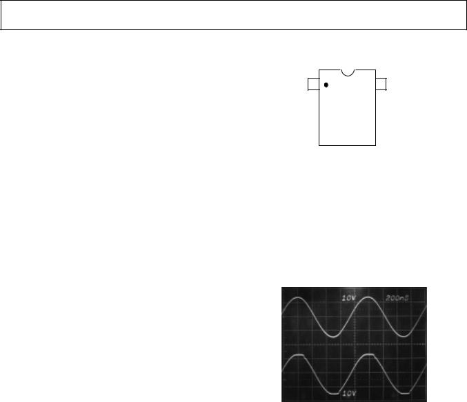
a LowHighCost,SpeedGeneralJFET AmplifierPurpose
AD825
FEATURES
High Speed
41 MHz, –3 dB Bandwidth
125 V/ s Slew Rate
80 ns Settling Time
Input Bias Current of 20 pA and Noise Current of 10 fA/√Hz
Input Voltage Noise of 12 nV/√Hz
Fully Specified Power Supplies: 5 V to 15 V
Low Distortion: –76 dB at 1 MHz High Output Drive Capability
Drives Unlimited Capacitance Load 50 mA Min Output Current
No Phase Reversal When Input Is at Rail Available in 8-Lead SOIC
APPLICATIONS
CCD
Low Distortion Filters
Mixed Gain Stages
Audio Amplifier
Photo Detector Interface
ADC Input Buffer
DAC Output Buffer
PRODUCT DESCRIPTION
The AD825 is a superbly optimized operational amplifier for high speed, low cost and dc parameters, making it ideally suited for a broad range of signal conditioning and data acquisition applications. The ac performance, gain, bandwidth, slew rate and drive capability are all very stable over temperature. The AD825 also maintains stable gain under varying load conditions.
The unique input stage has ultralow input bias current and ultralow input current noise. Signals that go to either rail on this high performance input do not cause phase reversals at the output. These features make the AD825 a good choice as a buffer for MUX outputs, creating minimal offset and gain errors.
The AD825 is fully specified for operation with dual ± 5 V and
± 15 V supplies. This power supply flexibility, and the low supply current of 6.5 mA with excellent ac characteristics under all supply conditions, makes the AD825 well suited for many demanding applications.
REV. C
Information furnished by Analog Devices is believed to be accurate and reliable. However, no responsibility is assumed by Analog Devices for its use, nor for any infringements of patents or other rights of third parties which may result from its use. No license is granted by implication or otherwise under any patent or patent rights of Analog Devices.
CONNECTION DIAGRAM
8-Lead Plastic SOIC (R) Package
NC 1 |
8 NC |
–IN |
2 |
AD825 |
7 |
+VS |
|
TOP VIEW |
|||||
|
|
|
|
||
|
|
(Not to Scale) |
|
|
|
+IN |
3 |
|
6 |
OUTPUT |
|
–VS |
|
|
|
|
|
|
|
|
|
||
4 |
|
5 |
NC |
||
|
|
|
|
|
NC = NO CONNECT
Figure 1. Performance with Rail-to-Rail Input Signals
One Technology Way, P.O. Box 9106, Norwood, MA 02062-9106, U.S.A.
Tel: 781/329-4700 |
World Wide Web Site: http://www.analog.com |
Fax: 781/326-8703 |
© Analog Devices, Inc., 1999 |
22

July 2008
TIP31/TIP31A/TIP31B/TIP31C
NPN Epitaxial Silicon Transistor
Features
• Complementary to TIP32/TIP32A/TIP32B/TIP32C
1. Base 2. Collector 3. Emitter
Absolute Maximum Ratings TC=25qC unless otherwise noted
Symbol |
|
Parameter |
Value |
Units |
|
|
|
|
|
VCBO |
Collector-Base Voltage |
: TIP31 |
40 |
V |
|
|
: TIP31A |
60 |
V |
|
|
: TIP31B |
80 |
V |
|
|
: TIP31C |
100 |
V |
|
|
|
|
|
VCEO |
Collector-Emitter Voltage |
: TIP31 |
40 |
V |
|
|
: TIP31A |
60 |
V |
|
|
: TIP31B |
80 |
V |
|
|
: TIP31C |
100 |
V |
|
|
|
|
|
VEBO |
Emitter-Base Voltage |
|
5 |
V |
IC |
Collector Current (DC) |
|
3 |
A |
ICP |
Collector Current (Pulse) |
|
5 |
A |
IB |
Base Current |
|
1 |
A |
|
|
|
|
|
PC |
Collector Dissipation (TC=25qC) |
40 |
W |
|
|
|
|
|
|
|
Collector Dissipation (Ta=25qC) |
2 |
W |
|
|
|
|
|
|
TJ |
Junction Temperature |
|
150 |
qC |
|
|
|
|
|
TSTG |
Storage Temperature |
|
- 65 ~ 150 |
qC |
Transistor Silicon Epitaxial NPN — TIP31/TIP31A/TIP31B/TIP31C
© 2008 Fairchild Semiconductor Corporation |
www.fairchildsemi.com |
TIP31/TIP31A/TIP31B/TIP31C Rev. A
23

July 2008
TIP32/TIP32A/TIP32B/TIP32C
PNP Epitaxial Silicon Transistor
Features
• Complementary to TIP31/TIP31A/TIP31B/TIP31C
1. Base 2. Collector 3. Emitter
Absolute Maximum Ratings TC=25qC unless otherwise noted
Symbol |
|
Parameter |
Value |
Units |
|
|
|
|
|
VCBO |
Collector-Base Voltage |
: TIP32 |
- 40 |
V |
|
|
: TIP32A |
- 60 |
V |
|
|
: TIP32B |
- 80 |
V |
|
|
: TIP32C |
- 100 |
V |
|
|
|
|
|
VCEO |
Collector-Emitter Voltage |
: TIP32 |
- 40 |
V |
|
|
: TIP32A |
- 60 |
V |
|
|
: TIP32B |
- 80 |
V |
|
|
: TIP32C |
-100 |
V |
|
|
|
|
|
VEBO |
Emitter-Base Voltage |
|
- 5 |
V |
IC |
Collector Current (DC) |
|
- 3 |
A |
ICP |
Collector Current (Pulse) |
|
- 5 |
A |
IB |
Base Current |
|
- 3 |
A |
|
|
|
|
|
PC |
Collector Dissipation (TC=25qC) |
40 |
W |
|
|
|
|
|
|
|
Collector Dissipation (Ta=25qC) |
2 |
W |
|
|
|
|
|
|
TJ |
Junction Temperature |
|
150 |
qC |
|
|
|
|
|
TSTG |
Storage Temperature |
|
- 65 ~ 150 |
qC |
Transistor Silicon Epitaxial PNP — TIP32/TIP32A/TIP32B/TIP32C
© 2008 Fairchild Semiconductor Corporation |
www.fairchildsemi.com |
TIP32/TIP32A/TIP32B/TIP32C Rev. A
24
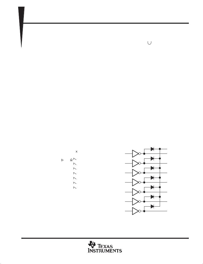
ULN2001A, ULN2002A, ULN2003A, ULN2004A
DARLINGTON TRANSISTOR ARRAYS
SLRS027 – DECEMBER 1976 – REVISED APRIL 1993
HIGH-VOLTAGE HIGH-CURRENT DARLINGTON TRANSISTOR ARRAYS
D500-mA Rated Collector Current (Single Output)
DHigh-Voltage Outputs . . . 50 V
DOutput Clamp Diodes
DInputs Compatible With Various Types of Logic
DRelay Driver Applications
DDesigned to Be Interchangeable With Sprague ULN2001A Series
description
D OR N PACKAGE
(TOP VIEW)
1B |
|
1 |
16 |
|
1C |
|
|
||||
|
|
|
|
2C |
|
2B |
|
2 |
15 |
|
|
|
|
|
|
3C |
|
3B |
|
3 |
14 |
|
|
|
4 |
13 |
|
4C |
|
4B |
|
|
|||
|
5 |
12 |
|
5C |
|
5B |
|
|
|||
|
6 |
11 |
|
6C |
|
6B |
|
|
|||
|
7 |
10 |
|
7C |
|
7B |
|
|
|||
|
8 |
9 |
|
COM |
|
E |
|
|
|||
|
|
|
|
|
|
The ULN2001A, ULN2002A, ULN2003A, and ULN2004A are monolithic high-voltage, high-current Darlington transistor arrays. Each consists of seven npn Darlington pairs that feature high-voltage outputs with common-cathode clamp diodes for switching inductive loads. The collector-current rating of a single Darlington pair is 500 mA. The Darlington pairs may be paralleled for higher current capability. Applications include relay drivers, hammer drivers, lamp drivers, display drivers (LED and gas discharge), line drivers, and logic buffers. For 100-V (otherwise interchangeable) versions, see the SN75465 through SN75469.
The ULN2001A is a general-purpose array and can be used with TTL and CMOS technologies. The ULN2002A is specifically designed for use with 14to 25-V PMOS devices. Each input of this device has a zener diode and resistor in series to control the input current to a safe limit. The ULN2003A has a 2.7-kΩ series base resistor for each Darlington pair for operation directly with TTL or 5-V CMOS devices. The ULN2004A has a 10.5-kΩ series base resistor to allow its operation directly from CMOS devices that use supply voltages of 6 to 15 V. The required input current of the ULN2004A is below that of the ULN2003A, and the required voltage is less than that required by the ULN2002A.
logic symbol†
|
|
|
CLAMP |
9 |
COM |
|
|
1 |
16 |
||||
1B |
|
|
|
1C |
||
|
|
|
||||
|
|
|
||||
|
|
|
|
|
||
2 |
|
|
|
15 |
||
2B |
|
|
|
2C |
||
|
|
|
|
|
||
3 |
|
|
|
14 |
||
3B |
|
|
|
3C |
||
|
|
|
|
|
||
4 |
|
|
|
13 |
||
4B |
|
|
|
4C |
||
5 |
|
|
|
12 |
||
5B |
|
|
|
5C |
||
|
|
|
||||
|
|
|
|
|
||
6 |
|
|
|
11 |
||
6B |
|
|
|
6C |
||
|
|
|
|
|
||
7 |
|
|
|
10 |
||
7B |
|
|
|
7C |
||
|
|
|
|
|
||
|
|
|
|
|
|
|
†This symbol is in accordance with ANSI/IEEE Std 91-1984 and IEC Publication 617-12.
logic diagram
|
1 |
9 |
COM |
1B |
16 |
1C |
|
|
|
||
2B |
2 |
15 |
2C |
|
|
||
3B |
3 |
14 |
3C |
|
|
||
4B |
4 |
13 |
4C |
|
|
||
5B |
5 |
12 |
5C |
|
|
||
6B |
6 |
11 |
6C |
7B |
7 |
10 |
7C |
|
|
PRODUCTION DATA information is current as of publication date. Products conform to specifications per the terms of Texas Instruments standard warranty. Production processing does not necessarily include testing of all parameters.
Copyright 1993, Texas Instruments Incorporated
POST OFFICE BOX 655303 • DALLAS, TEXAS 75265
25


Aureus TMS320DA708, TMS320DA708B, TMS320DA788B
Floating-Point Digital Signal Processors
www.ti.com
SPRS297E–JULY 2005–REVISED JULY 2007
1 Second Generation Aureus™ DSPs
1.1 Features
•DA708/B/DA788B: 32-/64-Bit 250-/266-MHz Floating-Point DSP
•Upgrades to C67x+ CPU From DA6xx Family:
–2X CPU Registers [64 General-Purpose]
–New Audio-Specific Instructions
–Compatible With the DA6xx C67x CPU
•Enhanced Memory System
–256K-Byte Unified Program/Data RAM
–768K-Byte Unified Program/Data ROM
–Single-Cycle Data Access From CPU
–Large Program Cache (32K-Byte) Supports RAM, ROM, and External Memory
•External Memory Interface (EMIF) Supports:
–100-/133-MHz SDRAM (16-Bit)
–Async NOR Flash, SRAM (8- or 16-Bit)
–NAND Flash (8- or 16-Bit)
•Enhanced I/O System
–High-Performance Crossbar Switch
–Dedicated McASP DMA Bus
–Deterministic I/O Performance
•dMAX Dual Data Movement Accelerator:
–Memory-to-Memory Transfers
–Memory-to-Peripheral Transfers
–Packing/Unpacking Delay Data
–Circular Addressing
–Non-Sequential Addressing for Reverb
•Three Multichannel Audio Serial Ports
–Transmit/Receive Clocks up to 50 MHz
–Five Clock Zones and 16 Serial Data Pins
–Supports TDM, I2S, and Similar Formats
–DIT Only (McASP2)
•Two 10-MHz SPI Ports With 3-, 4-, and 5-Pin Options
•Two Inter-Integrated Circuit (I2C) Ports
•Real-Time Interrupt Counter/Watchdog
•Oscillatorand Software-Controlled PLL
•Commercial or Extended Temperature
•144-Pin, 0.5-mm, PowerPAD™ Thin Quad Flatpack (TQFP) [RFP Suffix]
•Security Features Available
•Applications
–A/V and DVD Receiver
–Multizone A/V Receiver
–HDD Jukebox
–Navigation Systems
–High-Speed Encode With Simultaneous Multichannel Decode
•Software Support
–Dolby® Digital, Dolby® Digital EX, Dolby® Digital Plus, Dolby® TrueHD,
Dolby® Pro Logic® IIx, Dolby® Headphone, Dolby® Virtual Surround,
–DTS®5.1, DTS-ES™ 6.1, DTS Neo:6™, DTS 96/24™, DTS-ES 96/24™, DTS-HD™ (DA788B only)
–MPEG-2 AAC LC Decode
–MPEG-4 AAC LC Encode/Decode
–THX® Select 2, THX® Ultra 2, Neural-THX® Surround
–MP3 Encode, MP3 Decode
–WMA8 Encode, WMA9 Decode
–HDCD® Decode
–ATRAC3plus® Encode, ATRAC3plus® Decode
–Audyssey MultEQ XT®, MultEQ®, PrevEQ®, 2EQ®
–SRS® Circle Surround™ II (CS II)
–TI Bass Boost
–TI Perfect Playback™ Compressed Audio Enhancer
–TI Virtualizer/Headphone
–TI Effects Library
–TI DSD-to-PCM Decode
–TI Filter Library
–TI Performance Audio Framework (PA/F)
–TI DSP/BIOS™
–Chip Support Library and DSP Library
Please be aware that an important notice concerning availability, standard warranty, and use in critical applications of Texas Instruments semiconductor products and disclaimers thereto appears at the end of this document.
PRODUCTION DATA information is current as of publication date. |
Copyright © 2005–2007, Texas Instruments Incorporated |
Products conform to specifications per the terms of the Texas |
|
Instruments standard warranty. Production processing does not |
|
necessarily include testing of all parameters. |
|
27

Aureus TMS320DA708, TMS320DA708B, TMS320DA788B
Floating-Point Digital Signal Processors
www.ti.com
SPRS297E–JULY 2005–REVISED JULY 2007
1.2 Trademarks
Aureus, Perfect Playback, DSP/BIOS, PowerPAD, TMS320C6000, C6000, Code Composer Studio, XDS, TMS320, TMS320C62x, and TMS320C67x are trademarks of Texas Instruments.
Audyssey MultEQ XT, MultEQ, PrevEQ, and 2EQ are registered trademarks of Audyssey Laboratories. SRS is a registered trademark of SRS Labs, Inc. in the U.S. and selected foreign countries.
Circle Surround II is a trademark of SRS Labs, Inc.
DTS-ES, DTS Neo:6, DTS 96/24, DTS-ES 96/24, and DTS-HD are trademarks of Digital Theater Systems, Inc.
DTS is a registered trademark of Digital Theater Systems, Inc.
Dolby and Pro Logic are registered trademarks of Dolby Laboratories. Philips is a registered trademark of Koninklijki Philips Electronics N.V.
HDCD is a registered trademark of Microsoft Corporation in the United States and/or other countries. ATRAC3plus is a registered trademark of Sony Corporation in Japan and/or other countries/territories. THX is a registered trademark of THX Ltd.
All trademarks are the property of their respective owners.
Second Generation Aureus™ DSPs |
Submit Documentation Feedback |
28
 Loading...