

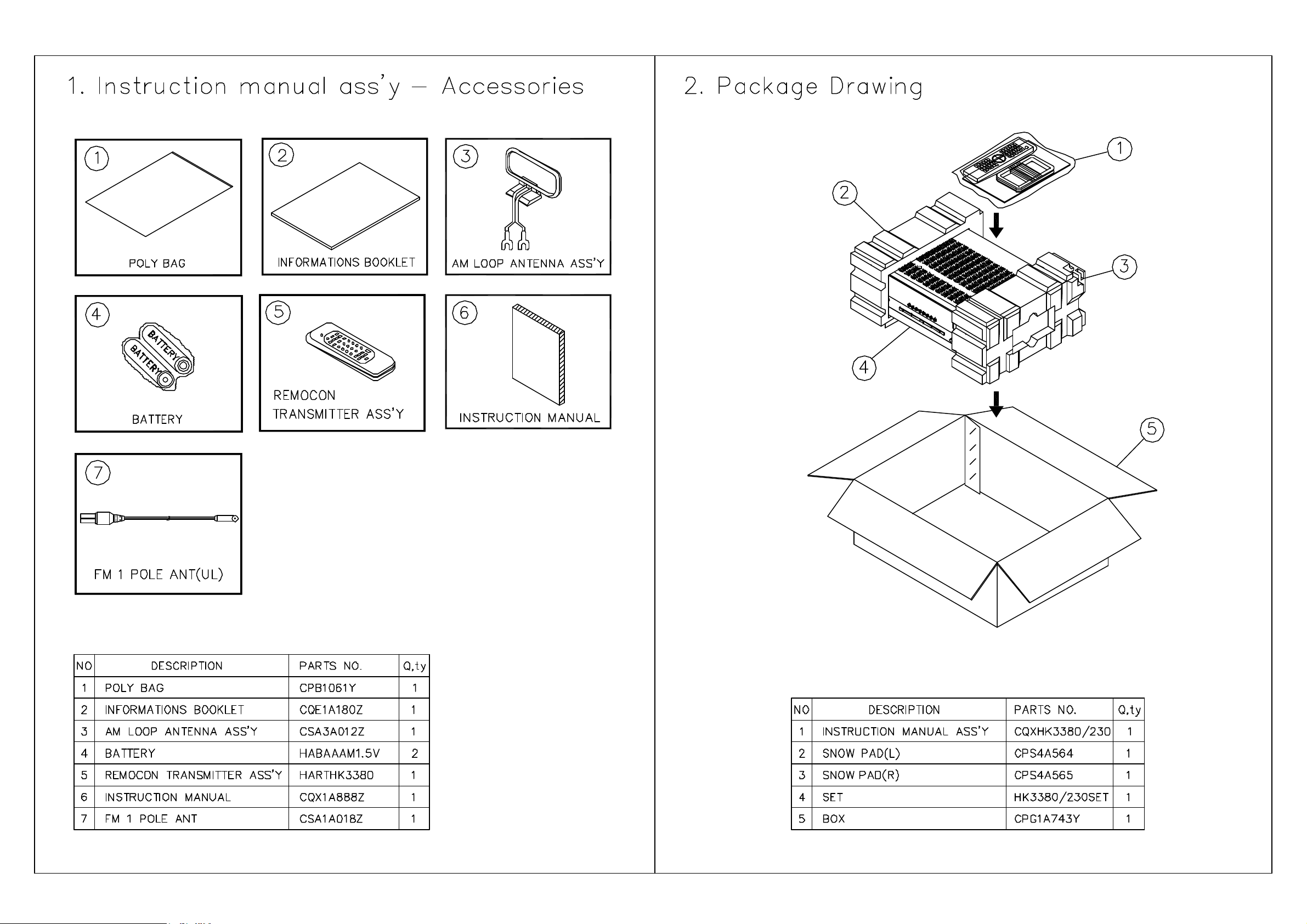
Page 1
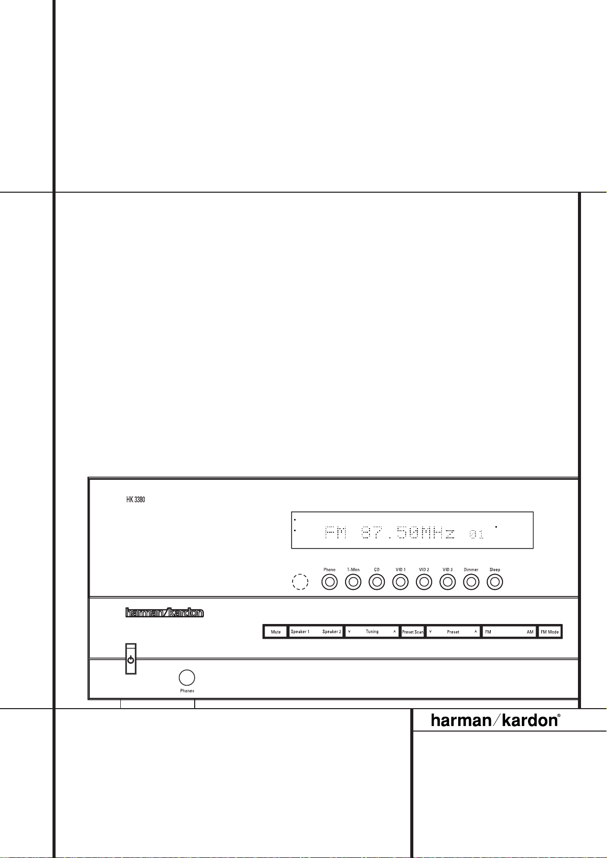
HK 3380 HK3480 Stereo Receiver
SERVICE MANUAL
Power for the Digital Revolution
®
SPEAKER 1
SPEAKER 2
MUTE
AUTO
TUNED
STEREO
RDS
PTY CT RT TA
PHONO
MEMORY
PRESET
SLEEP
VID 1
FM
VID 2
AM
VID 3
TAPE M.
CD
Page 2

TECHNICAL SPECIFICATIONS HK3380
Technical Specifications HK3380/230
Audio Section
Stereo Mode
Continuous Average Power (FTC)
80 Watts per channel, 20Hz –20kHz
@ < 0.07% THD, both channels driven into 8 ohms
100 Watts per channel, 20Hz–20kHz
@ < 0.2% THD, both channels driven into 4 ohms
Input Sensitivity/Impedance
Linear (High Level) 200mV/47kohms
Signal-to-Noise Ratio (IHF-A) 95dB
Frequency Response
@ 1W (+0dB, –3dB) 10Hz– 110kHz
High Instantaneous
Current Capability (HCC) ±42 Amps
Transient Intermodulation
Distortion (TIM) Unmeasurable
Rise Time 16 µsec
Slew Rate 40V/µsec
FM T uner Section
Frequency Range 87.5 –108MHz
Usable Sensitivity IHF: 1.12 µV/13.5dBf
Signal-to-Noise Ratio Mono/Stereo: 73/72dBA (DIN)
Distortion Mono/Stereo: 0.3/0.4%
Stereo Separation 40dB @ 1kHz
Selectivity ±400kHz, 65dB
Image Rejection >80dB
IF Rejection >100dB
AM T uner Section
Frequency Range 520 –1710kHz
Signal-to-Noise Ratio >40dB
Usable Sensitivity Loop: 500µV/M
Distortion 1kHz, 50% Mod: 0.8%
Selectivity ±10kHz: >25dB
Video Section
Television System NTSC/PAL/SECAM
Signal Format Composite
Input Level 1Vp-p
Input Impedance 75 ohms, unbalanced
Sync Polarity Negative
Output Level 1Vp-p
Output Impedance 75 ohms, unbalanced
Video Frequency
Response 10Hz – 10MHz
General
Power Requirement AC 230V/50Hz
Power Consumption 3W standby, 200W maximum
(both channels driven)
Dimension (Max)
Width 442mm
Height 168mm
Depth 382mm
Weight 9.5kg
Depth measurement includes knobs, buttons and terminal connections. Height measurement includes feet and chassis.
All features and specifications are subject to change without notice.
Harman Kardon and Power for the Digital Revolution are registered trademarks of Harman International Industries,Incorporated.
Page 3
Technical Specifications HK3480
Audio Section
Stereo Mode
Continuous Average Power (FTC)
100 Watts per channel, 20Hz–20kHz
@ < 0.07% THD, both channels driven into 8 ohms
135 Watts per channel, 20Hz–20kHz
@ < 0.2% THD, both channels driven into 4 ohms
Input Sensitivity/Impedance
Linear (High Level) 200mV/47kohms
Signal-to-Noise Ratio (IHF-A) 95dB
Frequency Response
@ 1W (+0dB, –3dB) 10Hz– 110kHz
High Instantaneous
Current Capability (HCC) ±40 Amps
Transient Intermodulation
Distortion (TIM) Unmeasurable
Rise Time 16 µsec
Slew Rate 40V/µsec
FM T uner Section
Frequency Range 87.5 –108MHz
Usable Sensitivity IHF: 1.12 µV/13.5dBf
Signal-to-Noise Ratio Mono/Stereo: 71/67dBA (DIN)
Distortion Mono/Stereo: 0.3/0.4%
Stereo Separation 40dB @ 1kHz
Selectivity ±300kHz, 60dB
Image Rejection >80dB
IF Rejection >100dB
AM T uner Section
Frequency Range 520 –1710kHz
Signal-to-Noise Ratio >40dB
Usable Sensitivity Loop: 500µV/M
Distortion 1kHz, 50% Mod: 0.8%
Selectivity ±9kHz: >25dB
General
Power Requirement AC 230V/50Hz
Power Consumption 72W idle, 470W maximum
(both channels driven)
Dimension (Max)
Width 442mm
Height 156mm
Depth 415mm
Weight 12.1kg
Depth measurement includes knobs, buttons and terminal connections. Height measurement includes feet and chassis.
All features and specifications are subject to change without notice.
Harman Kardon is a registered trademark, and Power for the digital revolution is a trademark, of Harman Kardon, Inc.
VMAx is a registered trademark of Harman International Industries, Inc.,and is an implementation of Cooper Bauck Transaural Stereo under patent license.
TECHNICAL SPECIFICATIONS HK3480
Page 4

DISASSEMBLY PROCEDURES
<1> TOP-CABINET(21) REMOVAL
1. Remove 13 screws(S1) and then remove the Top-cabinet.
<2> FRONT PANEL ASS’Y REMOVAL
1. Remove the Top-cabinet, referring to the previous step<1>.
2. Disconnect the lead wire(BN71-12P,BN72-5P) on the Tone PCB(38) from connector(CN71,CN72) on the
Main PCB(44).
3. Disconnect the lead wire(BN82-7P) on the Front PCB(37) from connector(CN82) on the Main PCB(44).
4. Disconnect the connector(CN81-20P wire assy) on the Front PCB(37) from connector(CN81)
on the Main PCB(44).
5. Disconnect the lead wire(BN73-3P) on the Phone PCB(40) from connector(CN73) on the Main PCB(44).
6. Disconnect the lead wire(BN89-7P) on the Front PCB(37) from connector(CN73) on the Download PCB(44).
7. Remove 1 screw(S10) and then lead wire(JW73-2P) on the Phone PCB(40).
8. Remove 1 screw(S10) and then lead wire(JW72-1P) on the Tone PCB(38).
9. Remove 9 screws(S1) and then remove the Front Panel ASS’Y.
<3> TONE PCB(38) REMOVAL
1. Remove the Top-cabinet, referring to the previous step<1>.
2. Remove the Front Panel ASS’Y, referring to the previous step<2>.
3. Pull out the Volume Knob ASS’Y & 3 Rotary Knobs(5).
4. Remove 9 screws(S1,S11) and then remove the Tone PCB(38).
5. Disconnect the lead wire(BN83-4P) from connector(CN83) on the Tone PCB(38).
<4>PHONE PCB(40) REMOVAL
1. Remove the Top-cabinet, referring to the previous step<1>.
2. Remove the Front Panel ASS’Y, referring to the previous step<2>.
3. Remove 2 screws(S2,S3) and then remove the Phone PCB(16).
<5>POWER LED PCB(39) REMOVAL
1. Remove the Top-cabinet, referring to the previous step<1>.
2. Remove the Front Panel ASS’Y, referring to the previous step<2>.
3. Remove 2 screws(S2) and then remove the Power led PCB(39).
4. Disconnect the lead wire(BN84-4P) from connector(CN84) on the Power led PCB(39).
<6>FRONT PCB(37) REMOVAL
1. Remove the Top-cabinet, referring to the previous step<1>.
2. Remove the Front Panel ASS’Y, referring to the previous step<2>.
3. Remove the Tone PCB(38), referring to the previous step<3>.
4. Remove the Phone PCB(40), referring to the previous step<4>.
5. Remove the Power led PCB(39), referring to the previous step<5>.
6. Remove 13 screws(S2) and then remove the Front PCB(37).
<7>TUNER MODULE(34) REMOVAL
1. Remove the Top-cabinet, referring to the previous step<1>.
2. Disconnect the connector(CON1-Card cable) from connector(CN26) on the Main PCB ASS’Y(44).
3. Remove 2 screws(S8) and then remove the Tuner Module(34).
Page 5

<8>VIDEO PCB(43) REMOVAL
1. Remove the Top-cabinet, referring to the previous step<1>.
2. Disconnect the connector (CN91) on the Main PCB ASS’Y(44) from lead wire(BN91-9P)
on the Video PCB(43).
3. Remove 4 screws(S8,S13) and then remove the Video PCB(43).
<9>DOWNLOAD PCB(42) REMOVAL
1. Remove the Top-cabinet, referring to the previous step<1>.
2. Disconnect the connector (CN89) from lead wire(BN89-7P) on the Front PCB(37).
3. Remove 2 screws(S4) and then remove the Download PCB(42).
<10>POWER TRANS(30) REMOVAL
1. Remove the Top-cabinet, referring to the previous step<1>.
2. Disconnect the connector (CN62,CN63,CN64) on the Trans PCB from lead wire(BN62-2P,BN63-3P,BN64-6P)
on the Main PCB(44).
3. Remove 4 Trans screws(S9) and then remove the Power Trans(30).
<11>MAIN PCB ASS’Y(44) REMOVAL
1. Remove the Top-cabinet, referring to the previous step<1>.
2. Remove the Power Trans(30), referring to the previous step<10>.
3. Disconnect the connector(CN81-20P wire ass’y) from connector(CN81-7P) on the Front PCB(37).
4. Disconnect the connector(CN82) from lead wire(BN82-7P) on the Front PCB(37).
5. Disconnect the connector(CN71) from lead wire(BN71-12P) on the Tone PCB(38).
6. Disconnect the connector(CN72) from lead wire(BN72-5P) on the Tone PCB(38).
7. Disconnect the connector(CN73) from lead wire(BN73-3P) on the Phone PCB(40).
8. Disconnect the connector(CN91) from lead wire(BN91-9P) on the Video PCB(43).
9. Disconnect the connector(CN26-Card cable) from lead wire(CON1) on the Tuner Module(34).
10. Disconnect the connector(CN61) from Power cord(35).
11. Remove 21 screws(S8-11EA, S13-1EA, S4-2EA, S6-2EA, S15-1EA, S12-3EA, S5-1EA) and then
remove the Main PCB ASS’Y(44).
Page 6
HK3380/230
HK3480/230
Page 7
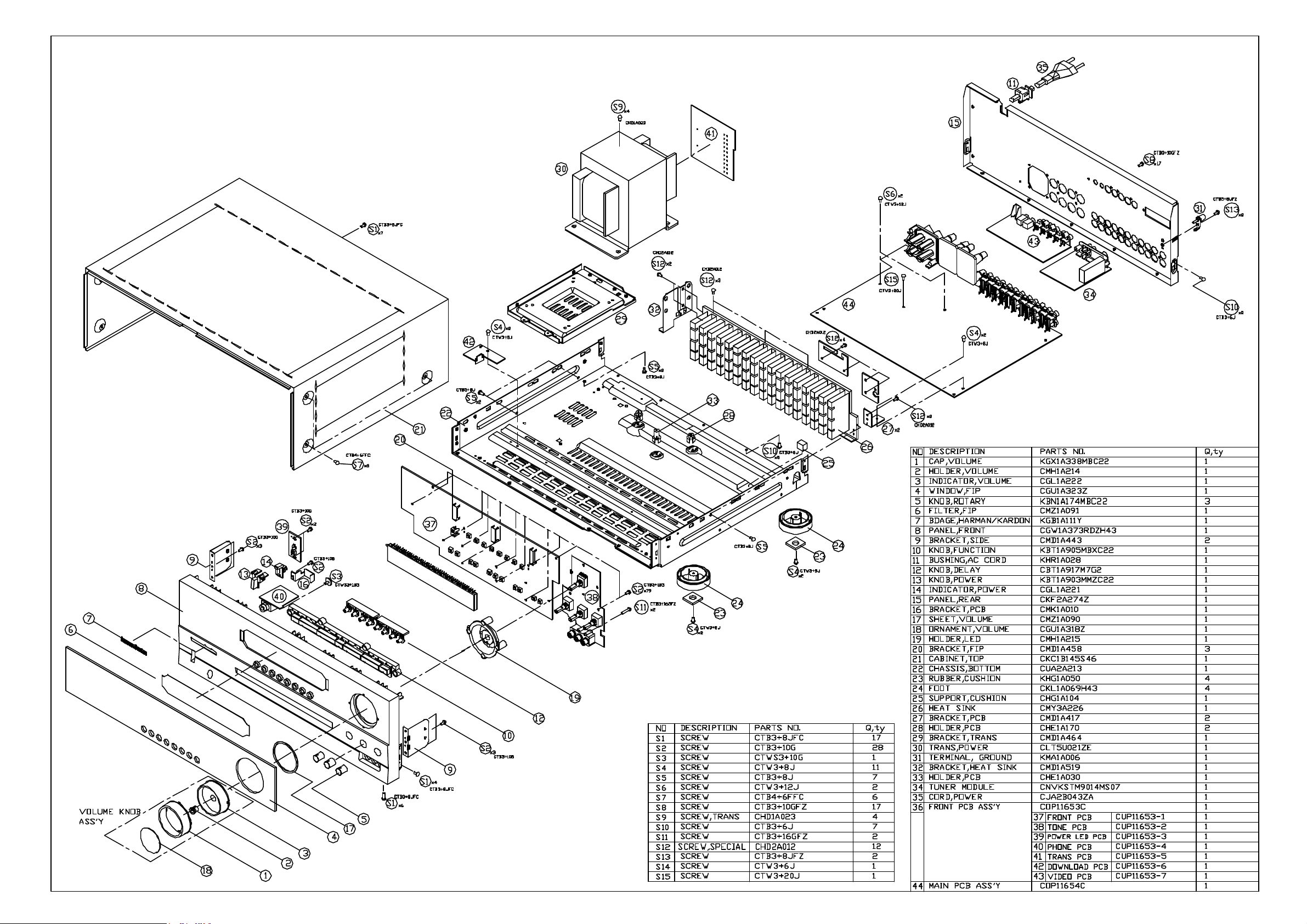
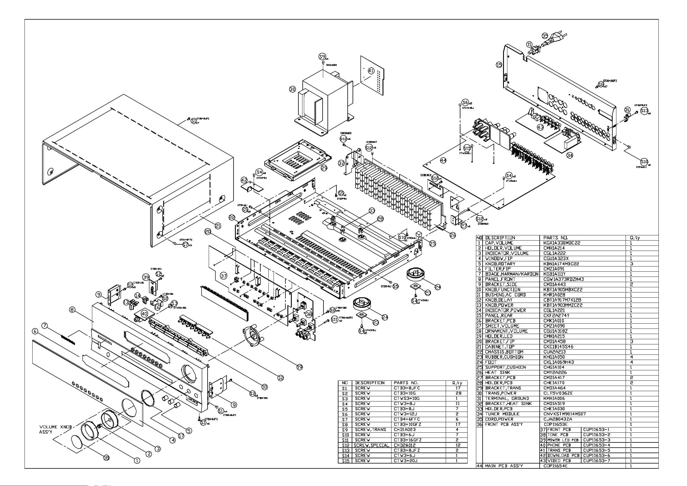
HK3380/230 EXPLODED VIEW
Page 8
HK3480/230 EXPLODED VIEW
Page 9
HK3380/230
Page 10

HK3480/230
Page 11

FRONT PCB CUP11653Y (VIDEO PCB CUP11653-7) HK3380/230
REF NO. PART NO. 1st DESCRIPTION 2nd DESCRIPTION
▶CAPACITOR
C603,604,605,606 HCQI1H473JZT CAP , MYLAR 0.047UF 50V J
C701,702,711~714
C802,817
C703,704,726 HCBS1H101KBT CAP , CERAMIC 100PF 50V K
C707, 708 CCEA1CKS470T CAP , ELECT 47UF/16V
C709,710,813,814 HCBS1H470JT CAP , CERAMIC 47PF 50V J
C715,716,719,720 KCFE1J183JBT CAP , FILM 0.018UF 63V J
C717,718 KCFE1J823JBT CAP , FILM 0.082UF 63V J
C721,722 KCFE1J332JBT CAP , FILM 0.0033UF 63V J
C723,724 HCBS1H221KBT CAP , CERAMIC 220PF 50V K
C727,744,808,809
C819,838,839,914
C728,729,730,804
C811,815,816,818
C830,834,837,911
C912,828
C741,742 HCQI1H122JZT CAP , MYLAR 1200PF 50V J
C745 HCBS1H103ZFT CAP , CERAMIC 0.01UF 50V Z
C801 CCKT1H104ZF CAP , CERAMIC 50V 0.1UF
C803,812 CCEA1AH471T CAP , ELECT 470UF 10V
C805,806 HCBS1H150JCT CAP , CERAMIC 15PF 50V
C807,823,824,840 HCBS1H821KBT CAP , CERAMIC 820PF 50V K
C810, 829 CCEA1AKS101T CAP. ELECT 100UF 10V
C820 CCEA1CH331T CAP , ELECT 330UF 16V
C821 CCEA1CKS4R7T CAP. ELECT 4.7UF 16V
C822 HCBS1H151KBT CAP , CERAMIC 150PF 50V K
C831 CCEA1CKS2R2T CAP , ELECT HK3480 only 2.2UF 16V
C832,833 HCBS1H102KBT CAP , CERAMIC 1000PF 50V K
C835 CCEA0JH102T CAP , ELECT 1000UF 6.3V
C904~908 CCKT1H101KB CAP , CERAMIC 100PF 50V KB
C909,910,921,922 CCEA1CH101T CAP , ELECT 100UF 16V
C913 CCEA1EH220T CAP , ELECT 22UF/25V
C825, 826 HCBS1H390JT CAP , CERAMIC 39PF 50V J
C827 HCBS1H561KBT CAP , CERAMIC 560PF 50V K
▶DIODE
D701~705 CVD52CSBBCEAB2 BLUE L.E.D
D706 CVD50BOGDWGA L.E.D , 2 COLOR
D707,708,802~808
D901~903
▶COIL
L801 HLQ02C100KT COIL , AXAIL
▶TRANSISTOR
Q801,803,805,807
Q808,813
Q802,806,814,901 HVTKRA107MT T.R KRA107M
Q804 HVTKTA1271YT T.R KTA1271Y
Q809 KVTKSA1175YT T.R KSA1175Y
Q810 KVTKSC2785YT T.R KSC2785Y
Q811,812 HVTKSC945CYT T.R KSC945CY
CCEA1HKS100T CAP , ELECT UF10 50V KS
HCBS1H104ZFT CAP , CERAMIC 0.1UF 50V Z
HCBS1H223ZFT CAP , CERAMIC 0.022UF 50V Z
HVD1SS133MT DIODE 1SS133T-77
HVTKRC107MT T.R KRC107M
Page 12

FRONT PCB CUP11653Y (VIDEO PCB CUP11653-7) HK3380/230
REF NO. PART NO. 1st DESCRIPTION 2nd DESCRIPTION
▶RESISTOR
R705,706,829,830
R870,918,871
R701,702,707,708
R709,710,723,724
R711,712 CRD20TJ105T RES , CARBON 1M OHM 1/5W J
R713,714 CRD20TJ223T RES , CARBON 22K OHM 1/5W J
R715,716,919 CRD20TJ392T RES , CARBON 3.9K OHM 1/5W J
R717,718,824,872 CRD20TJ222T RES , CARBON 2.2K OHM 1/5W J
R719,720 CRD20TJ681T RES , CARBON 680 OHM 1/5W J
R721,722,745 CRD20TJ471T RES , CARBON 470 OHM 1/5W J
R725,901~905 CRD20TJ750T RES , CARBON 75 OHM 1/5W J
R726 CRD20TJ560T RES , CARBON 56 OHM 1/5W J
R727,728,820,856
R866
R729,809,825~827
R835,853,860,863
R908,911,912,913
R873,874
R733,734 CRD20TJ331T RES , CARBON 330 OHM 1/5W J
R742,828,833,834
R836,909,910,877
R744 CRD20TJ181T RES , CARBON 180 OHM 1/5W J
R801 CRD20TJ122T RES , CARBON 1.2K OHM 1/5W J
R806,807,808,822
R823,837~839,841
R842,845,847~852
R876,818
R831,832,844,846 CRD20TJ472T RES , CARBON 4.7K OHM 1/5W J
R843,857,867,906
R907,917
R854,861,864 CRD20TJ152T RES , CARBON 1.5K OHM 1/5W J
R855,862,865 CRD20TJ182T RES , CARBON 1.8K OHM 1/5W J
R858,868 CRD20TJ562T RES , CARBON 5.6K OHM 1/5W J
R859,869 CRD20TJ752T RES , CARBON 7.5K OHM 1/5W J
R875 CRD20TJ820T RES , CARBON 82 OHM 1/5W J
R878 CRD20TJ273T RES , CARBON 27K OHM 1/5W J
R915 CRD20TJ271T RES , CARBON 270 OHM 1/5W J
R916 CRD20TJ470T RES , CARBON 47 OHM 1/5W J
R920 CRD20TJ473T RES , CARBON 47K OHM 1/5W J
R921,922 CRG2ANJ470H RES , METAL OXIDE FILM 47 OHM 2W J
▶TACT SWITCH
S701,801~819 HST1A020ZT SW , TACT
▶WIRE ASS'Y
BN71 CWZHK3380BN71 WIRE ASS'Y
BN72 CWZHK3380BN72 WIRE ASS'Y
BN73 CWB2B903350EN WIRE ASS'Y
BN82 CWB2B907350EN WIRE ASS'Y
BN83,84 CWB2B904070EN WIRE ASS'Y
BN89 CWB2B907160EN WIRE ASS'Y
BN91 CWB2B909200EN WIRE ASS'Y
BN81 CWZHK3380BN81 WIRE ASS'Y
CRD20TJ101T RES , CARBON 100 OHM 1/5W J
CRD20TJ104T RES , CARBON 100K OHM 1/5W J
CRD20TJ272T RES , CARBON 2.7K OHM 1/5W J
CRD20TJ102T RES , CARBON 1K OHM 1/5W J
CRD20TJ100T RES , CARBON 10 OHM 1/5W J
CRD20TJ103T RES , CARBON 10K OHM 1/5W J
CRD20TJ332T RES , CARBON 3.3K OHM 1/5W J
Page 13

FRONT PCB CUP11653Y (VIDEO PCB CUP11653-7) HK3380/230
REF NO. PART NO. 1st DESCRIPTION 2nd DESCRIPTION
▶CONNECTOR
CN62 KJP02GA89ZM WAFER MOLEX35328-02
CN63 KJP03GA90ZM WAFER MOLEX35313-0310
CN64 KJP06GA01ZM WAFER MOLEX 5267-06A
CN81 CJP20GB163ZW WAFER
CN83,84 KJP04GA19ZM WAFER
CN89 KJP07GA19ZM WAFER MOLEX53014-0710
CN90 KJP07HA37ZM WAFER
▶F.I.P
FIP1 HFLHCA16ML08-1 F.I.P
▶I.C
IC71 HVINJM2068MDTE1 I.C , OP AMP NJM2068MD-TE1
IC81 HVIST72F321R I.C , FLASH U-COM
IC82 BVISAA6579TV1 I.C , RDS FILTER SAA6579T/V1
IC83 HVIAT24C08N10SC I.C AT24C08N10SC2.7
IC84 HVIS-80145ALMC I.C RESET S-80145ALMC
IC85 HVIRE5VL28CATZ I.C , RESET
IC87 HVIL7805CP I.C, REGULATOR
IC88 HVIL7905CP I.C, REGULATOR
IC91 HVINJM2296M I.C , VIDEO SW NJM2296M
IC92 BVIKP1010B I.C, PHOTO COUPLER
▶JACK
JK71 CJJ2E026Z JACK , HEADPHONE
JK72 CJJ4S023Y JACK , BOARD
JK91 CJJ4N043Z JACK , BOARD
JK92 CJJ4S010Z JACK , BOARD
JK93,94 CJJ2D008Z JACK , STEREO
JW72 CWE8202110RV WIRE, ASS'Y
JW73 CWZAVR2550JW82 WIRE , ASS'Y
▶REMOCON SENSER
RC81 HRVKSM603TH2 REMOCON SENSER CN KSM-603TH2
▶VARIABLE RESISTOR
VR71,72 CVV2X07C104Z RES , VARIABLE(TONE) RK14128030214C
VR73 CVV2X05M104Z RES , VARIABLE(BALANCE) RK14128030214Y
▶ENCODER
VR81 HSR2A026Z VR , ENCODER
▶CRYSTAL
X801 HOX04000E150C CRYSTAL , 4MHZ
X802 HOX04332E200C CRYSTAL , 4.332MHZ
Page 14

PCB, MAIN CUP11654Y HK3380/230
REF NO. PART NO. 1st DESCRIPTION 2nd DESCRIPTION
▶CAPACITOR
C101,102,105,106 CCKT1H101KB CAP , CERAMIC 100PF 50V KB
C103,104,117,118
C191~194,301,302
C107,108,111,112
C121,122,123,124
C175,176,181,182
C195,196,219,220
C305,306
C307~310 HCEA1JH471E CAP , ELECT HK 3480 only 470UF 63V
C109,110,213,214
C222
C113,114,331~336 HCQI1H562JZT CAP , MYLAR 5600PF 50V J
C115,116 HCQI1H152JZT CAP , MYLAR 1500PF 50V J
C119,120 HCQI1H183JZT CAP , MYLAR 0.018UF 50V J
C125~130 HCBS1H471KBT CAP , CERAMIC 470PF 50V K
C131~144 HCBS1H221KBT CAP , CERAMIC 220PF 50V K
C145,146 HCBS1H104ZFT CAP , CERAMIC 0.1UF 50V Z
C183~185,303,304 CCKT1H471KB CAP , CERAMIC 470PF 50V KB
C197,198,342,615
C616,623,624,627
C201~204 HCBS1H101KBT CAP , CERAMIC 100PF 50V K
C211,212,215
C216,341,620
C240 CCEA1HH1R0T CAP , ELECT 1UF 50V
C311,312 HCBS1H120JCT CAP , CERAMIC 12PF 50V J
C313,314 HCBS1H330JT CAP , CERAMIC 33PF 50V
C315,316,317 CCEA1HH100TS CAP , ELECT 10UF/50V 105'C
C318 CCEA1HH100T CAP. ELECT 10UF/50V
C319,320,607~609 HCQI1H473JZT CAP , MYLAR 0.047UF 50V J
C343 CCEA1AH471T CAP , ELECT 470UF 10V
C351,352 HCBS1H681KBT CAP , CERAMIC 680PF 50V K
C401,402,405,406 CCEA1EH470T CAP , ELECT HK 3480 only 47UF 25V
C409 KCFE1J334JBT CAP , FILM HK 3480 only 0.33UF 63V J
C613,614,622 CCEA1EH101T CAP , ELECT 100UF 25V
C619,629 CCEA1HH470T CAP , ELECT 47UF/50V
C626 CCEA1AH101T 100UF 10V
C628,630 HCBS1H103ZFT CAP , CERAMIC 0.01UF 50V Z
C307~310 CCEA1JH221E CAP , ELECT 220UF 63V
C601,602 CCET63VKL5103NK CAP , ELECT HK 3380 only 10000/63V
C601,602 CCET63VKL5153NK CAP , ELECT HK 3480 only 15000UF 63V
C611 HCEA1EH332E CAP , ELECT 3300UF 25V
C612 CCEA1EH222E CAP. ELECT. 2200UF 25V
C621 KCKDKS472ME CAP , CERAMIC(X1/Y2/SC) 0.0047UF/2.5KV
C625 CCEA1EH102E CAP , ELECT 1000UF 25V
C631 BCQE2E104KDE CAP , LINE ACROSS 0.1UF 250V KD
C632 CCEA1JH101E CAP , ELECT 100UF 63V
▶DIODE
D101~110,112~115
D301~309,606,612
D613,614
D602~605,607,615
D616~618
D608,609 HVDMTZJ15BT DIODE , ZENER 15V 1/2W
D611 HVDMTZJ6.2BT DIODE , ZENER 6.2V 1/2W
D601 HVDGBJ806MF DIODE , BRIDGE
CCEA1VH100T CAP , ELECT 10UF 35V
CCEA1CH101T CAP , ELECT 100UF 16V
HCQI1H102JZT CAP , MYLAR 1000PF 50V J
CCKT1H223ZF CAP , CERAMIC 0.022UF 50V ZF
CCEA1HH4R7T CAP , ELECT 4.7UF 50V
HVD1SS133MT DIODE 1SS133T-77
KVD1N4003ST DIODE 1N4003
Page 15

PCB, MAIN CUP11654Y HK3380/230
REF NO. PART NO. 1st DESCRIPTION 2nd DESCRIPTION
▶COIL
L101,102 HLQ02C470KT COIL , AXAIL
▶TRANSISTOR
Q204~208 HVTKTC2874BT T.R , MUTE KTC2874B
Q209,332,337,338
Q602
Q210,335,336 HVTKRC107MT T.R KRC107M
Q301~306,311,312 HVTKTC3200GRT T.R KTC3200GR
Q307~310 HVTKTA1268GRT T.R KTA1268GR
Q323,324,333,334
Q601
Q331 KVTKSA1175YT T.R KSA1175Y
Q603 HVTKTA1271YT T.R KTA1271Y
Q313,314 HVTKTA1360Y T.R , PRE DRIVE KTA1360Y
Q315,316 HVTKTC3423Y T.R , PRE DRIVE KTC3423Y
Q317 HVTKTC3114A T.R , BIAS KTC3114A
Q318 HVTKTC3114A T.R , BIAS KTC3114A
Q319 BVT2SD2401P T.R , POWER(DARINGTON)
Q320 BVT2SD2401P T.R , POWER(DARINGTON)
Q321 BVT2SB1570P T.R , POWER(DARINGTON)
Q322 BVT2SB1570P T.R , POWER(DARINGTON)
▶RESISTOR
R101,102,359,360
R363,364,386
R103~106,117,118
R213,214,221,222
R618
R107,108,121,123
R124,171,172,181
R182,195,196,201
R202~204,219,220
R109,110 CRD20TJ564T RES , CARBON 560K OHM 1/5W J
R111,112,173,174
R367,368,385
R113,114 CRD20TJ751T RES , CARBON 750 OHM 1/5W J
R115,116,125~144
R183~185,211,305
R306
R122 CRD25TJ101T RES , CARBON 100 OHM 1/4W J
R151~164 CRD20TJ474T RES , CARBON 470K OHM 1/5W J
R191~194,205~208 CRD20TJ184T RES , CARBON 180K OHM 1/5W J
R212 CRD25TJ471T RES , CARBON 470 OHM 1/4W J
R215,216 CRD20TJ202T RES , CARBON 2K OHM 1/5W J
R217,218,617 CRD20TJ222T RES , CARBON 2.2K OHM 1/5W J
R223,224,315~318
R384
R234 CRD20TJ562T RES , CARBON 5.6K OHM 1/5W J
R235~239 CRD20TJ332T RES , CARBON 3.3K OHM 1/5W J
R240,365,366 CRD20TJ103T RES , CARBON 10K OHM 1/5W J
R241 CRD20TJ822T RES , CARBON 8.2K OHM 1/5W J
R255 CRD20TJ105T RES , CARBON 1M OHM 1/5W J
R303,304,319,320
R383
HVTKRA107MT T.R KRA107M
KVTKSC2785YT T.R KSC2785Y
CRD20TJ102T RES , CARBON 1K OHM 1/5W J
CRD20TJ104T RES , CARBON 100K OHM 1/5W J
CRD20TJ101T RES , CARBON 100 OHM 1/5W J
CRD20TJ473T RES , CARBON 47K OHM 1/5W J
CRD20TJ471T RES , CARBON 470 OHM 1/5W J
CRD20TJ152T RES , CARBON 1.5K OHM 1/5W J
CRD20TJ333T RES , CARBON 33K OHM 1/5W J
Page 16

PCB, MAIN CUP11654Y HK3380/230
REF NO. PART NO. 1st DESCRIPTION 2nd DESCRIPTION
R307,308 CRD20TJ100T RES , CARBON 10 OHM 1/5W J
R309,310 CRD20TJ271T RES , CARBON 270 OHM 1/5W J
R311~314 CRD20TJ221T RES , CARBON 220 OHM 1/5W J
R321,322,343,344
R611
R323~334 CRD20TJ561T RES , CARBON 560 OHM 1/5W J
R335~338 CRD20TJ750T RES , CARBON 75 OHM 1/5W J
R339~342 CRD20TJ223T RES , CARBON 22K OHM 1/5W J
R345,346 CRD20TJ331T RES , CARBON 330 OHM 1/5W J
R347~350,621 KRD25FJ3R3T RES , CARBON 3.3 OHM 1/4W J
R351~354 KRD25FJ180T RES , CARBON 18 OHM 1/4W J
R357,358 CRD20TJ511T RES , CARBON 510 OHM 1/5W J
R361,362,609,610
R619,620
R371~374 CRD25TJ470T RES , CARBON 47 OHM 1/4W J
R381,382 CRD20TJ273T RES , CARBON 27K OHM 1/5W J
R383 CRD20TJ433T RES , CARBON HK 3480 only 43K OHM 1/5W J
R391~393 CRD20TJ470T RES , CARBON 47 OHM 1/5W J
R601~604 CRD25TJ393T RES , CARBON 39K OHM 1/4W J
R607,608 CRD20TJ123T RES , CARBON 12K OHM 1/5W J
R612,613 CRD20TJ560T RES , CARBON 56 OHM 1/5W J
R614 CRD20TJ820T RES , CARBON 82 OHM 1/5W J
R355,356 CRF5EKR22HX2 RES , CEMENT 0.22OHM(*2), 5W
R375,376 CRG1ANJ100H RES , METAL OXIDE FILM 10 OHM 1W J
R377,378 CRG1ANJ221H RES , METAL OXIDE FILM 220 OHM 1W J
R605,606 KRQ1AJR47H RES , FUSE 0.47 OHM 1W J
R615 KRQ1AJ100H RES , FUSE 10 OHM 1W J
R427 CRD20TJ151T RES , CARBON HK 3480 only 150 OHM 1/5W J
R413,414 CRD20TJ220T RES , CARBON HK 3480 only 22 OHM 1/5W J
R434 CRD20TJ4R7T RES , CARBON HK 3480 only 4.7 OHM 1/5W J
R426,429,430,435 CRD20TJ512T RES , CARBON HK 3480 only 5.1K OHM J
R421,423 CRD20TJ622T RES , CARBON HK 3480 only 6.2K OHM 1/5W J
▶SEMI RESISTOR
VR31,32 HVN1RA221B01T RES , SEMI FIXED(220 OHM) RH0615C100221
▶WIRE ASS'Y
BN62 CWB4FA32120PU WIRE ASS'Y
BN63 CWB3FE03280UP WIRE ASS'Y
BN64 CWB1C906200BM WIRE ASS'Y
JW31 CWE7202050AA WIRE ASS'Y
JW32 CWE7202070AA WIRE ASS'Y
JW33 CWE7202060AA WIRE ASS'Y
JW34,35 CWE7202090AA WIRE ASS'Y
▶CONNECTOR
CN26 CJP13GA115ZY WAFER , CARD CABLE
CN31,32 KJP02GA01ZM WAFER MOLEX 5267-02A
CN61 KJP02KA060ZY WAFER 7.92MM(YUNHO)
CN71 KJP12GA19ZM WAFER
CN73,74 KJP03GA19ZM WAFER
CN75 KJP02GA19ZM WAFER
CN81 CJP20GA147ZW 20 DUAL WAFER JWT
CN82 KJP07GA19ZM WAFER MOLEX53014-0710
CN91 KJP09GA19ZM WAFER MOLEX53014-0910
▶I.C
IC11,14,16,21
IC41~43
IC12 HVITC9164AF I.C , FUNCTION TC9164AF
IC13 HVITC9163AF I.C , FUNCTION TC9163AF
IC15 HVITC9459F I.C , VOLUME
IC61 HVIL7805CP I.C, REGULATOR
IC64 CVIL7815CPVA I.C ASS'Y
IC65 CVIL7915CPVA I.C ASS'Y
CRD20TJ122T
CRD20TJ182T RES , CARBON 1.8K OHM 1/5W J
HVINJM2068MDTE1 I.C , OP AMP NJM2068MD-TE1
RES , CARBON 1.2K OHM 1/5W J
Page 17

PCB, MAIN CUP11654Y HK3380/230
REF NO. PART NO. 1st DESCRIPTION 2nd DESCRIPTION
▶JACK
JK10 CJJ4N060Z JACK , BOARD 2P (GOLD)
JK11,12 CJJ4P014W JACK , IN/OUT
JK13 CJJ4R019W TERMINAL , IN/OUT
JK14 CJJ4R021W JACK , IN/OUT
JK15 CJJ5Q006Z TERMINAL , SPEAKER
▶COIL
L301,302 CLEY0R5KAK COIL , SPEAKER 0.5UH K
▶OUTLET
OL61 KJJ7A025Z OUTLET , EUR (2P) A3-04-D007-2P
▶RELAY
RY31,32 HSL4A004ZU RELAY OSA-SS-212DM3
RY61 HSL1A008ZE RELAY SDT-S-112DMR
▶POSISTOR
TH31 KRTP42T7D330B
THERMAL SENSOR , POSISTOR
P42T7D330BW20
▶SUB TRANS
T602 CLT5J033ZE TRANS , SUB
▶CARD CABLE
BN26 CWC1C4A13B170B CARD , CABLE
▶FUSE
F601 KBA2C4000TLEY FUSE HK3380/230 T 4A L 250V
F601 KBA2C6300TLEY FUSE HK3480/230 T 6.3A L 250V
F602 KBA2D2500TLET FUSE T 2.5A L 250V
F603,604 KBA2C6300TLEY FUSE HK3380/230 T 6.3A L 250V
F603,604 KBA2C8000TLEY FUSE HK 3480/230 T 8A L 250V
▶OTHERS
T601 CLT5U021ZE TRANS , POWER HK3380/230
CLT5V036ZE TRANS , POWER HK3480/230
Page 18

Page 19

Page 20

Page 21

Page 22

Page 23

Page 24

KB1010B
NJM2068
DISPLAY
SAA6579TV1 RE5VL28
SAA6579
Page 25

2 PIN DESCRIPTION
Figure 2. 64-Pin TQFP 14x14 and 10x10 Package Pinout
/ SCLI
(HS) PE4
(HS) PE5
(HS) PE6
(HS) PE7
PWM3 / PB0
PWM2 / PB1
PWM1 / PB2
PWM0 /PB3
ARTCLK /(HS) PB4
ARTIC1 / PB5
ARTIC2 / PB6
PB7
AIN0 / PD0
AIN1 / PD1
AIN2 / PD2
AIN3 / PD3
EVD
/ ICCSEL
PP
PA7 (HS)
V
RESET
PA6 (HS) / SDAI
_2
DD
PE3
PE2
64 63 62 61 60 59 58 57 56 55 54 53 52 51 50 49
1
V
PE1 / RDI
PE0 / TDO
_2
SS
OSC1
OSC2
V
TLI
2
3
4
5
6
ei2
7
ei0
8
9
10
ei3
11
12
13
14
15
16
17 18 19 20 21 22 23 24 29 30 31 3225 26 27 28
SSA
AREF
V
V
AIN4 / PD4
AIN5 / PD5
AIN6 / PD6
AIN7 / PD7
ei1
SS_3
DD_3
V
V
(HS) PF2
BEEP / (HS) PF1
MCO / AIN8 / PF0
ICAP2_A / AIN11 / PF5
OCMP2_A / AIN9 / PF3
OCMP1_ A / AI N10 / PF4
PA5 (HS)
PA4 (HS)
V
48
SS_1
V
47
DD_1
PA3 (HS)
46
PA2
45
PA1
44
PA0
43
PC7 / SS
42
PC6 / SCK / ICCCLK
41
PC5 / MOSI / AIN 14
40
PC4 / MISO / ICCDATA
39
PC3 (HS) / ICAP1_B
38
PC2 (HS) / ICAP2_B
37
PC1 / OCMP1_B / AIN 1 3
36
PC0 / OCMP2_B / AIN12
35
V
34
V
33
ICAP1_A / (HS) PF6
EXTCLK_A / (HS) PF7
/ AIN15
SS_0
DD_0
(HS) 20mA high sink capability
eix associated external interrupt vector
Page 26

HVIST72F321R (U-COM) : IC81
Figure 1. Device Block Diagram
RESET
V
PP
TLI
V
SS
V
DD
EVD
OSC1
OSC2
PF7:0
(8-bits)
PE7:0
(8-bits)
PD7:0
(8-bits)
V
AREF
V
SSA
8-BIT CO RE
ALU
CONTROL
LVD
AVD
OSC
MCC/RTC/BEEP
PORT F
TIME R A
BEEP
PORT E
SCI
PORT D
10-BIT ADC
PROGRAM
MEMORY
(16K - 60K B yt es)
RAM
(512 - 2048 By tes)
WATCHDOG
ADDRESS AND DATA BUS
I2C
PORT A
PORT B
PWM ART
PORT C
TIMER B
SPI
PA7:0
(8-bits)
PB7:0
(8-bits)
PC7:0
(8-bits)
3
Page 27

Page 28

LEVEL SHIFTER
2
1
2
3
4
1
5
6
2
7
8
3
1
2
3
4
1
5
6
2
7
8
3
1
3
4
5
6
7
8
9
10
14 28
11
12
13
27
26
25
24
23
22
21
20
19
18
17
16
15
LATCH CIRCUIT
SHIFT REGISTER
LEVEL SHIFTER
LATCH CIRCUIT
L-S R-S
Vss GND VDD
L-S
L-S
L-S
L-COM
L-S
L-S
L-COM
L-S
L-S
L-COM
ST
R-S
R-S
R-S
R-COM
R-S
R-S
R-COM
R-S
R-S
R-COM
DATA
CK
LEVEL SHIFTER
2
1
2
3
1
4
5
6
2
7
8
3
1
2
3
1
4
5
6
2
7
8
3
1
3
4
5
6
7
8
9
10
14 28
11
12
13
27
26
25
24
23
22
21
20
19
18
17
16
15
LATCH CIRCUIT
SHIFT REGISTER
LEVEL SHIFTER
LATCH CIRCUIT
L-S R-S
Vss GND VDD
L-S
L-S
L-COM
L-S
L-S
L-S
L-COM
L-S
L-S
L-COM
ST
R-S
R-S
R-COM
R-S
R-S
R-S
R-COM
R-S
R-S
R-COM
DATA
CK
TC9164AF (FUNCTION/INPUT) : IC12
BLOCK DIAGRAM
TC9163AF (FUNCTION/INPUT) : IC13
BLOCK DIAGRAM
Page 29

Page 30

 Loading...