

Page 1
Harman Kardon Service Manual
CONTENTS
EXPLODED VIEW AND PARTS 14
FRONT PANEL CONTROLS 3
AVR 151, AVR151S
75W 5.1 CHANNEL A/V RECEIVER
REAR PANEL CONNECTORS 5
REMOTE CONTROL FUNCTIONS 7
PROCESSOR RESET 9
TROUBLESHOOTING 10
SPECIFICATIONS 11
PACKAGE DRAWING 12
DISASSEMBLY 13
Released EU2013 Harman Consumer Group, Inc. Rev 1.1, 05/2015
8500 Balboa Boulevard
Northridge, California 91329
PARTS LIST 15
BIAS ADJUSTMENT 39
SEMICONDUCTOR PINOUTS 40
PCB DRAWINGS 108
BLOCK DIAGRAMS 118
WIRING DIAGRAM 120
SCHEMATIC DIAGRAMS 121
Page 2
®
AVR1510, AVR151, AVR151S
Harman Kardon
AVR151, AVR151S
Service ManualService Manual
Page 2 of 131
Audio/video receiver
DTS Logo
DLNA Logo
Owner’s Manual
Page 3
AVR
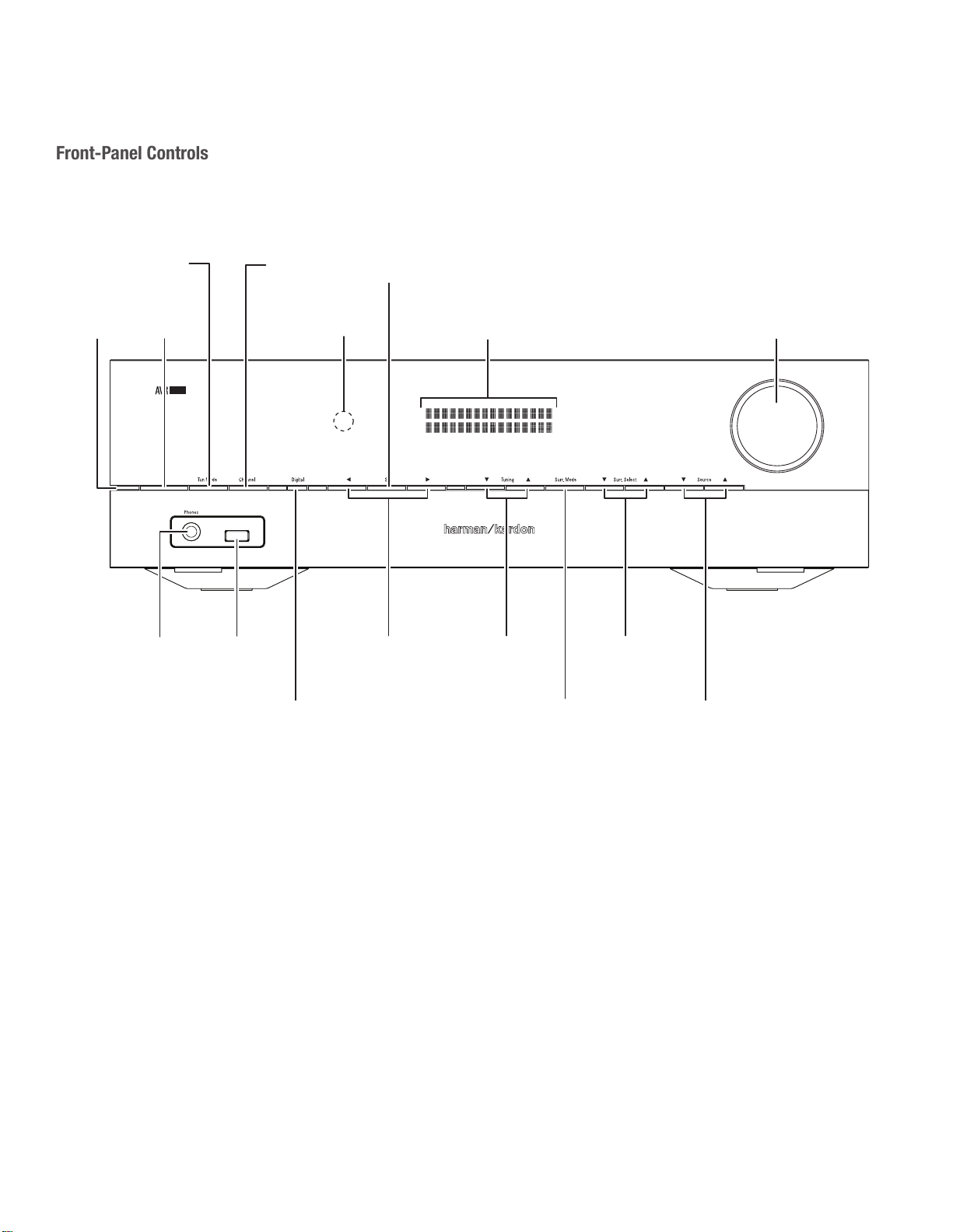
Front-Panel Controls
Front-Panel Controls
Harman Kardon
AVR151, AVR151S
Service ManualService Manual
Page 3 of 131
Tuning Mode Button
(AVR 1510)/ RDS
Button (AVR 151)
Power
Indicator
Power
Button
Headphone Jack
1510
USB
Port
Channel Volume
Adjust Button
IR
Sensor
Set
Button
Left/Right
Buttons
Front-Panel
Display
Up/Down Buttons/
Tuning Buttons
Volume
Knob
Surround Modes
Select Buttons
Audio Input
Button
4
Surround Mode
Category Button
Source Select
Buttons
Page 4

ENGLISH
AVR
Front-Panel Controls
Harman Kardon
AVR151, AVR151S
Service ManualService Manual
Page 4 of 131
Front-Panel Controls, continued
Power indicator/Power button: The AVR has three different power modes:
• Off (Power indicator glows solid amber): The Off mode minimizes energy
consumption when you’re not using the AVR. When the AVR is off, it will not
automatically turn on or play audio in response to a DLNA DMR stream from a
networked device. When the AVR is off, pressing the Power button turns it on.
To turn the AVR off when it is on, press the Power button for more than three
seconds. The Front-Panel Display will indicate “Your device is switched off” for
two seconds, then will switch off.
NOTE: You can use the System Setup menu to set the AVR to automatically
enter the off mode after it has been in the Sleep mode for a certain period of
time. See System Settings, on page 31.
• Sleep (Power indicator glows solid amber): The Sleep mode powers-down
some of the AVR’s circuitry, but allows the AVR to automatically turn on and
play audio in response to a DMR stream from a networked device. When the
AVR is in Sleep, pressing the Power button turns it on. To put the AVR into
Sleep when it is on, press the Power button for less than three seconds. The
message display will indicate “Device sleep” while the AVR is in the Sleep
mode.
NOTE: The AVR will automatically enter the Sleep mode after 30 minutes of no
audio signal or user control input, unless USB, iPod, Home Network, vTuner,
AirPlay, or DLNA DMR is active. In these cases, the AVR will automatically enter
the Sleep mode after the number of hours set in the Auto Power Off system
setting. See System Settings, on page 31.
• On (Power indicator glows solid white): When the AVR is on it is fully operational.
Headphone jack: Connect a 1/4" stereo headphone plug to this jack for private
listening.
Tuning Mode button (AVR 1510 only): Press this button to toggle the radio between
the manual (one frequency step at a time) and automatic (seeks frequencies with
acceptable signal strength) FM tuning mode. The button also toggles the radio
between stereo and mono modes when an FM station is tuned in.
RDS Button (AVR 151 only): When listening to an FM radio station that broadcasts
RDS information, this button activates the various RDS functions.
USB port: The USB port can be used to play audio les from an Apple iOS
connected to the port, and can also be used to play MP3 and WMA audio les from a USB
device inserted into the port. Insert the connector or device into the USB port oriented so
it ts all the way into the port. You may insert or remove the connector or device at any
time – there is no installation or ejection procedure.
You can also use the USB port to perform rmware upgrades. If an upgrade for the AVR’s
operating system is released in the future, you will be able to download it to the AVR using
this port. Complete instructions will be provided at that time.
IMPORTANT: Do not connect a PC or other USB host/controller to this port, or you
may damage both the AVR and the other device.
Channel Volume Adjust button: Press this button to activate the individual channel level
adjustment. After pressing this button, use the Up/Down buttons/Tuning buttons to select
the channel for adjustment and use the Left/Right buttons to adjust the channel’s level.
Audio Input button: Press this button to change the audio input connection for the current
source. Use the Left/Right buttons to cycle through the available input connections, and
press the Set button to assign the currently-displayed connection to the source.
IR sensor: This sensor receives infrared (IR) commands from the remote control. Make
sure that the sensor is not blocked.
Set button: Press this button to select the currently highlighted menu item.
Left/Right buttons: Use these buttons to navigate the AVR’s menus.
®
device
Front-panel display: Various messages appear on this two-line display in response
to commands and changes in the incoming signal. In normal operation, the current
source name appears on the upper line, while the active surround mode is displayed
on the lower line. When the on-screen display menu system (OSD) is in use, the
current menu settings appear.
Up/Down buttons/Tuning buttons: Use these buttons to navigate the AVR’s menus.
When the radio is the active source, use these buttons to tune stations according to the
setting of the Tuning Mode button (see above).
Surround Mode Category button: Press this button to select a surround-sound
category. Each press changes the surround-mode category: Auto Select, Virtual
Surround, Stereo, Movie, Music and Game. To change the specic surroundsound mode within the category, use the Surround Mode Select buttons. See
Audio Processing and Surround Sound, on page 30, for more information about
surround modes.
Surround Mode Select buttons: After you have selected the desired surround-mode
category, press these buttons to select a specic mode within the category, such
as to change from Dolby
Surround mode availability depends on the nature of the source input signal, i.e.,
digital versus analog, and the number of channels encoded within the signal.
Source Select buttons: Press these buttons to select the active source.
Volume knob: Turn this knob to raise or lower the volume.
®
Pro Logic® II Movie mode to DTS® NEO:6 Cinema mode.
5
Page 5
AVR
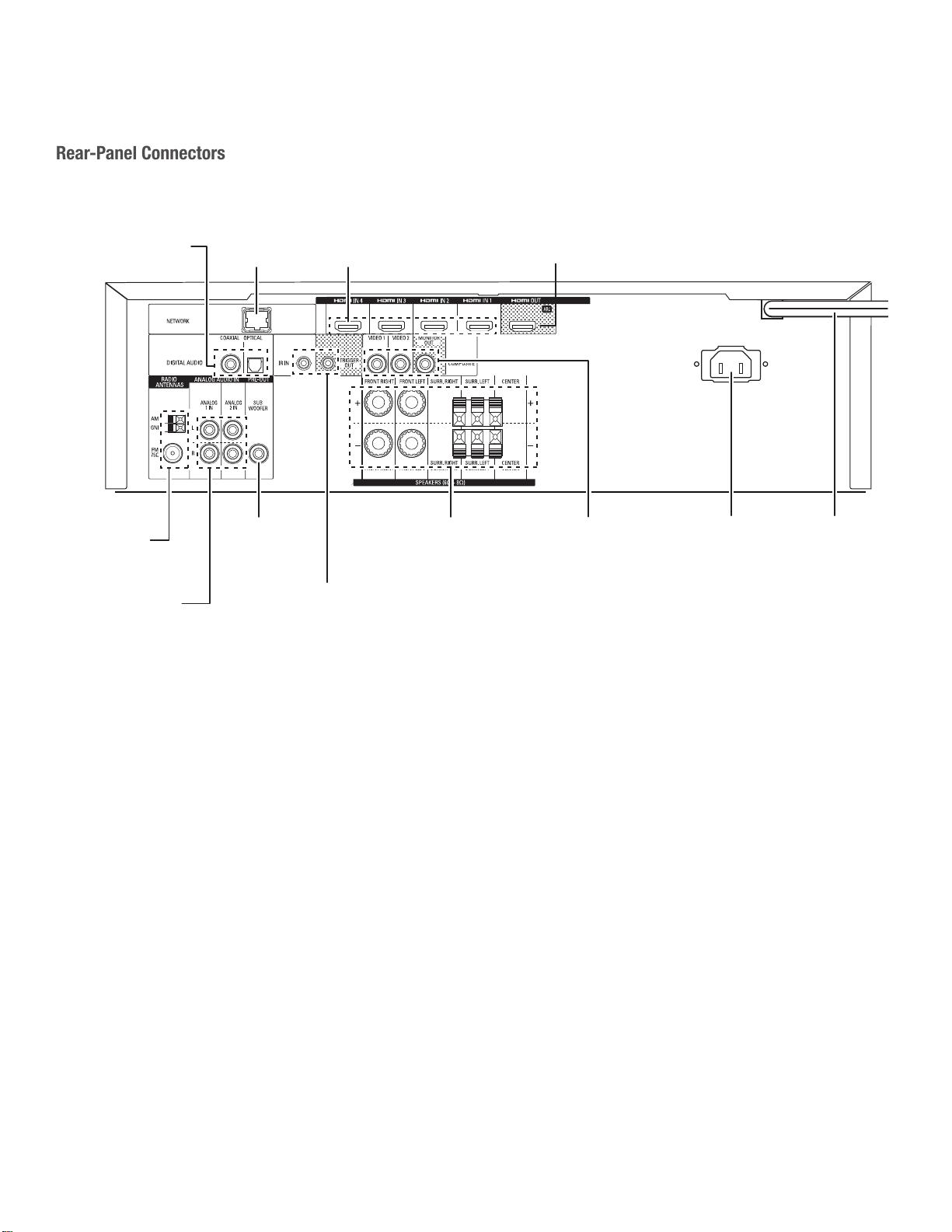
Rear-Panel Connectors
Rear-Panel Connectors
Harman Kardon
AVR151, AVR151S
Service ManualService Manual
Page 5 of 131
Digital Audio
Connectors
Radio Antenna
Connectors
Analog Audio
Connectors
Network
Connector
Subwoofer
Pre-Out
Connector
HDMI Input
Connectors
IR and Trigger
Connectors
Speaker
Connectors
HDMI Output
Connectors
Analog Video
Connectors
AC Input
Connector
(AVR 151)
Power Cord
(AVR 1510)
6
Page 6

ENGLISH
AVR
Rear-Panel Connectors, continued
Harman Kardon
AVR151, AVR151S
Service ManualService Manual
Page 6 of 131
Digital Audio connectors: If your non-HDMI source devices have digital outputs,
connect them to the AVR’s digital audio connectors. NOTE: Make only one type of
digital connection (HDMI, optical or coaxial) from each device. See Connect Your
Audio and Video Source Devices, on page 16, for more information.
Radio Antenna connectors: Connect the supplied AM and FM antennas to their
respective terminals for radio reception.
Analog Audio connectors: The following analog audio connectors are provided:
• Analog Audio Input connectors: Use the AVR’s Analog Audio Input connectors
for source devices that don’t have HDMI or digital audio connectors. See
Connect Your Audio and Video Source Devices, on page 16, for more
information.
Network connector: If your home network is wired, use a Cat. 5 or Cat. 5E Ethernet
cable (not supplied) to connect the AVR’s Network connector to your home
network to enjoy Internet radio and content from DLNA-compatible devices that
are connected to the network. See Connect to Your Home Network, on page 18,
for more information.
Subwoofer Pre-Out connector: Connect this jack to a powered subwoofer with a
line-level input. See Connect Your Subwoofer, on page 15, for more information.
IR and Trigger connector: The following IR and trigger connectors are provided:
• IR In connectors: When the IR sensor on the front panel is blocked (such as
when the AVR is installed inside a cabinet), connect an optional IR receiver to
the IR In jack.
• 12V Trigger connector: This connector provides 12V DC whenever the AVR
is on. It can be used to turn on and off other devices such as a powered
subwoofer.
HDMI Output connectors: If your TV has an HDMI connector and you are connecting
HDMI source devices to the AVR, use an HDMI cable (not included) to connect it to
the AVR’s HDM
I Out connector
Rear-Panel Connectors
®
HDMI
Input connectors: An HDMI connection transmits digital audio and video
signals between devices. If your source devices have HDMI connectors, using
them will provide the best possible video and audio performance quality. Since
the HDMI cable carries both digital video and digital audio signals, you do not have
to make any additional audio connections for devices you connect via the HDMI
connection. See Connect Your Audio and Video Source Devices, on page 16, for
more information.
AC Input connector (AVR 151 only): After you have made and veried all other
connections, plug the supplied AC power cord into this receptacle and into an
unswitched wall outlet.
Power cord (AVR 151 only): After you have made and veried all other connections,
plug the power cord into an unswitched wall outlet.
.
Notes on using the HDMI Output connector:
• When connecting a DVI-equipped display to the HDMI Out connector, use an
HDMI-to-DVI adapter and make a separate audio connection.
• Make sure the HDMI-equipped display is HDCP (High-bandwidth Digital
Content Protection)-compliant. If it isn’t, do not connect it via an HDMI
connection; use an analog video connection instead and make a separate
audio connection.
Speaker connectors: Use two-conductor speaker wire to connect each set of
terminals to the correct speaker. See Connect Your Speakers, on page 14, for more
information.
Analog Video connectors: The following Analog Video connectors are provided:
• Composite Video Input connectors: Use composite video connectors for video
source devices that don’t have HDMI connectors. You will also need to make an
audio connection from the source device to the AVR. See Connect Your Audio
and Video Source Devices, on page 16, for more information.
• Composite Video Monitor Out connector: If your TV or video display does
not have an HDMI connector, or if your TV does have an HDMI connector
but you are connecting some source devices with only composite video
connectors, use a composite video cable (not included) to connect the AVR’s
Composite Video Monitor Out connector to your TV ’s composite video input.
7
Page 7
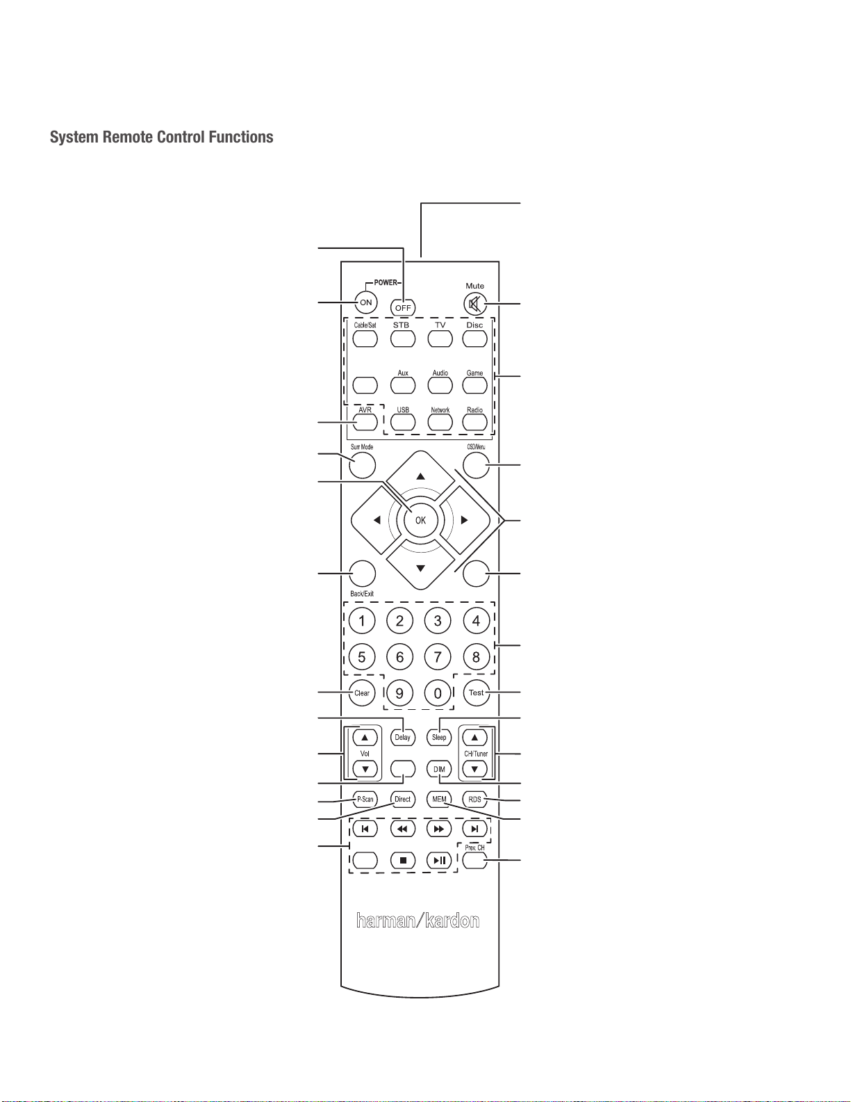
AVR
System Remote Control Functions
Power Off Button
Harman Kardon
AVR151, AVR151S
Service ManualService Manual
Page 7 of 131
System Remote Control Functions
IR Transmitter
Power On Button
AVR Button
Surround Modes Button
OK Button
Back/Exit Button
Clear Button
Server
Mute Button
Source Selector Buttons
OSD/Menu Button
Up/Down/Left/Right
Buttons
Info/Option Button
Info/Option
Number Buttons
Test Tone Button
Volume Up/Down Buttons
Transport Control Buttons
8
Delay Button
Tone Button
Preset Scan Button
Direct Button
Sleep Button
Channel/Tuner Buttons
Tone
Display Dimmer Button
RDS Button
Memory Button
TopMenu
Previous Channel Button
Page 8

ENGLISH
AVR
System Remote Control Functions
Harman Kardon
AVR151, AVR151S
Service ManualService Manual
Page 8 of 131
System Remote Control Functions, continued
In addition to controlling the AVR, the AVR remote is capable of controlling eight
other devices, including an iPod/iPhone device connected to the AVR’s frontpanel USB port. During the installation process, you may program the codes for
each of your source components into the remote. (See Program the Remote to
Control Your Source Devices and TV, on page 20, for programming information.)
To operate a component, press its Source Selector button to change the remote’s
control mode.
A button’s function depends on which component is being controlled. See Table
A13 in the Appendix for listings of the functions for each type of component. Most
of the buttons on the remote have dedicated functions, although the precise codes
transmitted vary depending on the specic device being controlled. Due to the wide
variety of functions for various source devices, we have included only a few of
the most-often used functions on the remote: number buttons, transport controls,
television-channel control, menu access and power on and off. Buttons dedicated
to the AVR – AVR Power On/Off, Surround Modes, Volume, Mute, Delay and Sleep
Settings – are available at any time, even when the remote is controlling another
device.
Power On/Power Off buttons: Press these buttons to turn the AVR on and put it
into Sleep or turn it off. See Power Indicator/Power Button, on page 5, for more
information.
IR Transmitter: As buttons are pressed on the remote, infrared codes are emitted
through this lens.
Mute button: Press this button to mute the AVR’s speaker-output connectors and
headphone jack. To restore the sound, press this button or adjust the volume.
Source Selector buttons: Press one of these buttons to select a source device, e.g.,
Disc, Cable/Sat, Radio, etc. This action will also turn on the AVR and switch the
remote’s control mode to operate the selected source device.
• The rst press of the Radio button switches the AVR to the last-used tuner band
(AM or FM). Each successive press changes the band.
• The rst press of the USB button switches the AVR to the last-used source
(USB or iPod). Each successive press cycles between the two sources.
• The rst press of the Network button switches the AVR to the last-used source
(Network or vTuner). Each successive press cycles between the two sources.
AVR button: Press to put the remote into the AVR control mode.
Surround Modes button: Press this button to access the Surround Modes submenu.
Select a surround-mode category: Auto Select, Virtual Surround, Stereo, Movie,
Music or Game. When you select the category, it is highlighted and the surround
mode changes.
To change the surround mode for the selected category navigate to the Surround
Mode menu in the AVR’s on-screen display menu, select the desired category, and
use the Left/Right buttons to select one of the available surround modes. See the
Advanced Functions section, on page 30, for more information.
OSD/Menu button: When the remote is controlling the AVR, press this button to
display the AVR’s on-screen display (OSD) menu. This button is also used within
the tuner menus and an iPod connected to the AVR’s front-panel USB port, and is
also used to display the main menu on some source devices.
OK button: This button is used to select items from the menu system. It is also used
to toggle between the Manual and Automatic tuning modes for FM or AM radio. To
toggle between these options, press and hold this button for more than 3 seconds.
Up/Down/Left/Right buttons: These buttons are used to navigate the menu system
and to operate the tuner.
Back/Exit button: Press this button to return to the previous menu or to exit the
menu system.
Info/Option button: Press to display the available option settings for the current
source.
Number buttons: Use these buttons to enter numbers for radio-station frequencies
or to select station presets.
Clear button: Press this button to clear a radio station frequency you have started
to enter.
Test Tone button: Press this button to activate test noise that will circulate through
each speaker, allowing you to adjust the individual speaker levels. Use the Up/Down
buttons to switch the noise to a different speaker and use the Left/Right buttons to
change the volume of the speaker the noise is playing through.
Delay Adjust button: Pressing this button lets you adjust two different types of delay
settings (use the Up/Down buttons to cycle through the settings):
• Lip Sync: This setting lets you resynchronize the audio and video signals from
a source to eliminate a “lip sync” problem. Lip-sync issues can occur when the
video portion of a signal undergoes additional processing in either the source
device or the video display. Use the Left/Right buttons to delay the audio by
up to 180ms.
• Distance: These settings let you set the delay for each speaker to compensate
for the different distances they may be from the listening position. Use the Up/
Down buttons to cycle through each of the system’s speakers, and use the Left/
Right buttons to set the distance each speaker is from the listening position.
See Congure the AVR for Your Speakers, on page 23, for more information.
Sleep button: Press this button to activate the sleep timer, which turns off the
receiver after a programmed period of time. Each press decreases the time by 10
minutes, down from 90 minutes – ending with the “Sleep Off” message.
Volume Up/Down buttons: Press these buttons to raise or lower the volume.
Channel/Tuner buttons: When radio has been selected, press these buttons to
select a preset radio station. While operating a cable, satellite or HDTV set-top box
or a television, press these buttons to change channels.
Tone button: Pressing this button lets you adjust the Tone settings for the current
source. Use the Left/Right buttons to switch between On and Off, or to adjust the
Bass or Treble from -10dB to +10dB. See Set Up Your Sources, on page 24, for
more information.
Display Dimmer button: Press this button to dim the AVR’s front-panel display
partially or fully.
Preset Scan button: When Radio is the selected source, press this button to play
each of your preset radio stations in order for ve seconds. Pressing the button
again to remain tuned to the current station.
Direct button: Press this button to directly tune to a radio station by using the
Number buttons to enter its frequency.
Memory button: Press this button to save the current radio station as a preset.
RDS button: When listening to an FM radio station that broadcasts RDS information,
this button activates the various RDS functions.
Transport Control buttons: These buttons are used to control source devices.
Previous Channel button: In AVR control mode, this button lets you adjust the output
levels for each speaker individually. Use the Up/Down buttons to cycle through
each speaker, and use the Left/Right buttons to set the level of that speaker. See
Congure the AVR for Your Speakers, on page 23, for more information. When TV
is the selected source, press this button to switch to the previously-tuned channel.
9
9
Page 9

AVR
Harman Kardon
AVR151, AVR151S
Service ManualService Manual
Page 9 of 131
System Settings
ENGLISH
System Settings
The AVR’s System Settings menu lets you customize in what way many of the AVR’s
features operate. Press the OSD/Menu button and navigate to the System line. Press the
OK button to display the System Settings menu.
Panel Timeout: This setting allows you to set the AVR’s front-panel display to automa tically
turn off after remaining on for a predertimined time (3 – 10 seconds) each time you use
a control. Set this to “Off” to have the display remain on continually.
Auto Power Off: This setting allows you to set the AVR to automatically switch to the Off
mode after being in the Sleep mode for a predetermined time (1 – 8 hours) and switch
to the Sleep mode after this amount of time if a source with an analog audio input or
internal source (FM, AM, USB, iPod, Home Network, vTuner or DMR) is active. See Power
Indicator/Power Button, on page 5, for more information.
Menu Timeout: This setting allows you to set the amount of time (20 – 50 seconds) a
menu screen will remain on after the last adjustment. Set this to “Off” to have the menus
remain on continually until you press the OSD/Menu button.
Status Message: When the AVR is turned on, the volume is adjusted, the source is
changed or a change in the input signal is detected, a status message will be displayed
on the TV screen. Select how long the message remains visible, from 2 to 10 seconds,
with a default of 3 seconds. Select “Off” if you do not wish to see the status messages on
the TV screen (they will still appear on the AVR’s front-panel message display).
Volume Default and Default Volume Setting: These two settings are used together to
program the volume level when you turn on the AVR. Set Volume Default to On, and then
set the Default Volume Setting to the desired turn-on volume. When Volume Default is
set to Off, the AVR will turn on at the last-used volume setting from the previous listening
session.
HDMI Audio to TV: This setting determines whether HDMI audio signals are passed
through the HDMI Monitor Out connector to the video display. In normal operation, leave
this setting at Off, as audio will be played through the AVR. To use the TV by itself, without
the home theater system, turn this setting to On. In this case you will need to mute the
TV’s speakers (or switch the setting to Off) when using the AVR for audio.
HDMI Link: This setting allows the communication of control information among the
HDMI devices in your system. Turn this setting to On to allow control communication
between the HDMI devices; turn the setting to Off to forbid control communication. When
this setting is set to Off, the TV source audio input is set to Optical. When this setting is
set to On, the TV source audio input is set to HDMI ARC.
Software Update: If a software upgrade is released for your AVR, installation instructions
will be available in the Product Support section of the Web site or from Harman Kardon
customer service. At that time, you may use this submenu to install the upgrade
software.
IMPORTANT: During a software upgrade, do not power off the AVR or use any of its
controls. Doing so could permanently damage the AVR.
Sleep Timer
The sleep timer sets the AVR to play for up to 90 minutes and then turn off
automatically.
Press the Sleep button on the remote, and the time until turn-off will be displayed. Each
additional press of the Sleep button decreases the play time by 10 minutes, from 90 to
10 minutes. The SLEEP OFF setting disables the sleep timer.
When the sleep timer has been set, the front-panel display will automatically dim to half
brightness.
If you press the Sleep button after the timer has been set, the remaining play time will be
displayed. Press the Sleep button again to change the play time.
Processor Reset
If the AVR behaves erratically after a power surge, unplug the AC power cord for at least
3 minutes. Plug the cord back in and turn the AVR on. If this procedure doesn’t help, reset
the AVR’s processor as described below.
NOTE:
A processor reset erases all user configurations, including speaker and level
settings, and tuner presets. After a reset, reenter all of these settings from your entries
in the Appendix worksheets.
To reset the AVR’s processor:
1. Press the front-panel Standby/On switch for more than three seconds to turn the AVR
off (the Power Indicator will turn amber).
2. Press and hold the front-panel Surround Modes button for at least 5 seconds until the
RESET message appears on the front-panel Message Display.
NOTE:
After performing a processor reset, wait at least 1 minute before pressing any
Source Selector buttons.
If the AVR does not function correctly after a processor reset, contact an authorized
Harman Kardon service center for assistance. Authorized service centers may be located
by visiting our Web site at www.harmankardon.com.
29
Page 10

ENGLISH
AVR
Symptom Cause Solution
Harman Kardon
AVR151, AVR151S
Service ManualService Manual
Page 10 of 131
Troubleshooting
Unit does not function • No AC power • Ensure that the power cord is plugged into a live AC
Front-panel display lights, but there’s no sound or
picture
No sound from any speaker
No sound from center or surround speakers • Incorrect surround mode
Unit does not respond to remote control commands • Weak batteries in remote
Intermittent buzzing in tuner
• Intermittent input connection
• Mute is on
• Volume control is turned down
• Amplier is in protection mode due to possible short
circuit
• Amplier is in protection mode due to internal
problems
• Program material is monophonic
• Incorrect speaker conguration
• Program material is stereo
• Remote sensor is obscured
• Local interference • Move the AVR or antenna away from computers,
power outlet
• Check if the AC outlet is switch-controlled
• Secure all input and speaker connections
• Press Mute button
• Turn up Volume control
• Check all speaker wires at speaker and AVR
connections for crossed wires
• Contact your local Harman Kardon service center
• Select a surround mode other than stereo
• Mono programs contain no surround information
• Check the speaker conguration in the setup menu
• The surround decoder may not create center- or
surround-channel information from nonencoded
programs
• Change batteries in remote
• Ensure that the AVR’s front-panel remote sensor is in
the line of sight of the remote
uorescent lights, motors or other electrical appliances
Unable to activate remote control Programming mode • Source Selector button is not held for at least 3
Unable to establish network connection
Additional information on troubleshooting possible problems with your AVR and installation-related issues may be found in the list of “Frequently Asked Questions,” which is
located in the Product Support section of our Web site: www.harmankardon.com
seconds
• AVR network programming requires rebooting • Cycle the AVR into the Off mode, and then turn it on
• Be sure to hold the Source Selector button for at least
3 seconds
again
33
Page 11
AVR
Specifications
Harman Kardon
AVR151, AVR151S
Service ManualService Manual
Page 11 of 131
Specifications
Audio Section
Stereo power:
Multichannel power:
Input sensitivity/impedance: 250mV/27k ohms
Signal-to-noise ratio (IHF-A): 100dB
Surround system adjacent channel
separation:
Frequency response (@ 1W): 10Hz – 130kHz (+0dB/–3dB)
High instantaneous current
capability (HCC):
Transient intermodulation
distortion (TIM):
Slew rate: 40V/μsec
FM Tuner Section
Frequency range: 87.5 – 108.0MHz
Usable sensitivity IHF: 1.3μV/13.2dBf
Signal-to-noise ratio (mono/stereo): 70dB/68dB
Distortion (mono/stereo): 0.2%/0.3%
Stereo separation: 40dB @ 1kHz
Selectivity (±400kHz): 70dB
Image rejection: 80dB
IF rejection: 80dB
75W per channel, two channels driven @
6/8 ohms, 1kHz, <0.9% THD
75W per channel, two channels driven @
6/8 ohms, 1kHz, <0.9% THD
Dolby Pro Logic/DPLII: 40dB
Dolby Digital: 55dB
DTS: 55dB
±28 amps
Unmeasurable
AM Tuner Section
Frequency range:
Signal-to-noise ratio: 38dB
Usable sensitivity (loop):
Distortion (1kHz, 50% mod): 1.0%
Selectivity (±10kHz): 30dB
520 – 1710kHz (AVR 1510)
522 – 1620kHz (AVR 151)
500µV
Video Section
Television format:
Input level/impedance: 1Vp-p/75 ohms
Output level/impedance: 1Vp-p/75 ohms
Video frequency response (composite
video):
HDMI:
NTSC (AVR 1510);
PAL (AVR 151)
10Hz – 8MHz (–3dB)
HDMI 1.4
General Specifications
Power requirement:
Power consumption:
Dimensions (W x H x D):
Weight
Depth measurement includes knobs, buttons and terminal connections.
Height measurement includes feet and chassis.
120V AC/60Hz (AVR 1510);
220V – 240V AC/50Hz – 60Hz (AVR 151)
<0.5W (standby);
410W maximum
17-5/16" x 4-3/4" x 11-13/16"
(440mm x 121mm x 300mm)
10 lb (4.6kg)
34
Page 12
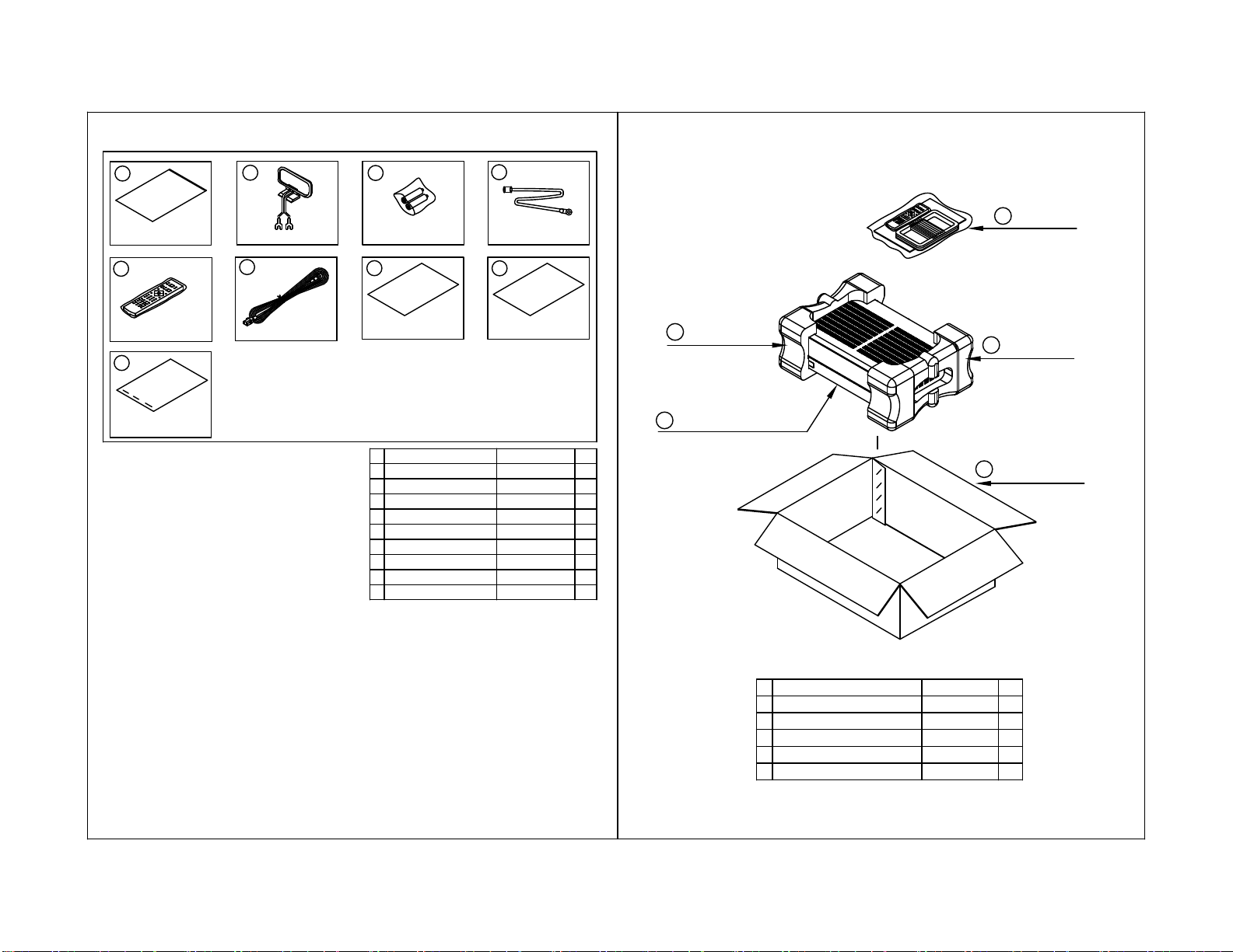
1. Instruction manual ass'y - Accessories(CQXAVR151/230)
Harman Kardon
AVR151, AVR151S
Service ManualService Manual
Page 12 of 131
2. Package Drawing
AVR151/230
1
POLY BAG
5
REMOCON
TRANSMITTER ASS'Y
9
STAPLE
2
AM LOOP ANTENNA ASS'Y
6
CORD , POWER(EUR)
3
BATTERY ASS'Y
7
SHEET,QUICK START GUIDE
NO DESCRIPTION PARTS NO. Q,ty
1
2
3
BATTERY
4
FM 1 POL ANT CSA1A018Z 1
5
REMOCON ASS'Y CARTAVR151-HK 1
CORD,POWER(PLUG+SOCKET)
6
7
SHEET,QUICK START GUIDE8CQE1A570Z
SHEET,SAFETY CQE1A601Z 1
9
STAPLE CPL0905 3
4
FM 1 POLE ANT(UL)
8
SHEET,SAFETY
CPB1A190ZPOLY BAG
CSA1A039ZANT, AM LOOP(9.5uH/5T)
CABR03PPB
CJA2B120Z 1
MANUAL ASS'Y
1
3
SNOW PAD (L)
SET
5
1
1
2
1
1
SNOW PAD (R)
4
BOX ,OUT CARTON
6
DESCRIPTIONNO
1
MANUAL ASS'Y
21PAD,LEFT
3
4
SET AVR151/230SET
BOX,OUT CARTON
5
CQXAVR151/230
CPS1A930
CPS1A931PAD,RIGHT
CPG1A972W
Q,tyPARTS NO.
1
1
1
1
Page 13
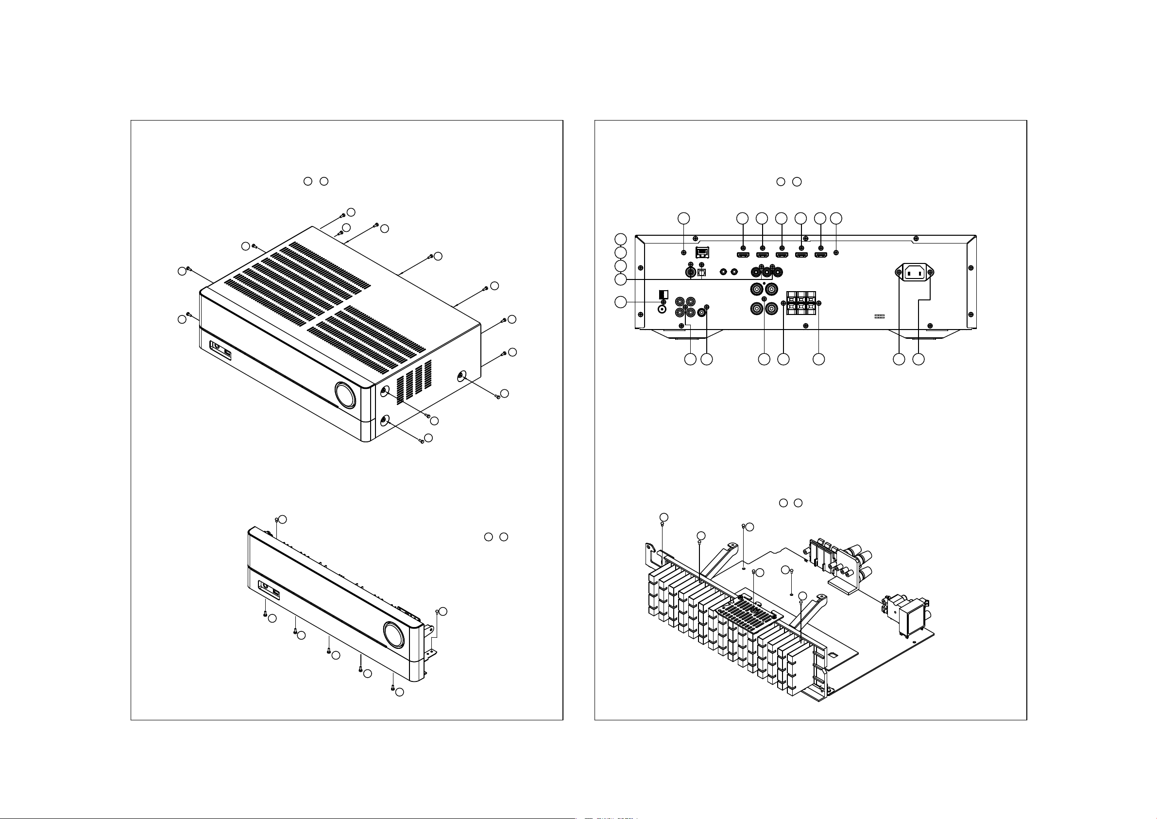
DISASSEMBLY
Harman Kardon
AVR151, AVR151S
Service Manual
Page 13 of 131
AVR151/230
1. Removing the Top Cabinet
13
Remove the Screws
5
6
4
1
~
10
11
3. Removing the Rear Panel
Remove the Screws
9
8
7
8
12
13
2
3
1
9
10
11
12
14 15 16 1713
19
1
~
1234567
18 19
4. Removing the Main PCB
1 6
Remove the Screws
1
7
6
2. Removing the Front Panel
Remove the Screws
2
5
4
3
1 7
~
4
6
3
2
~
5
1
Page 14
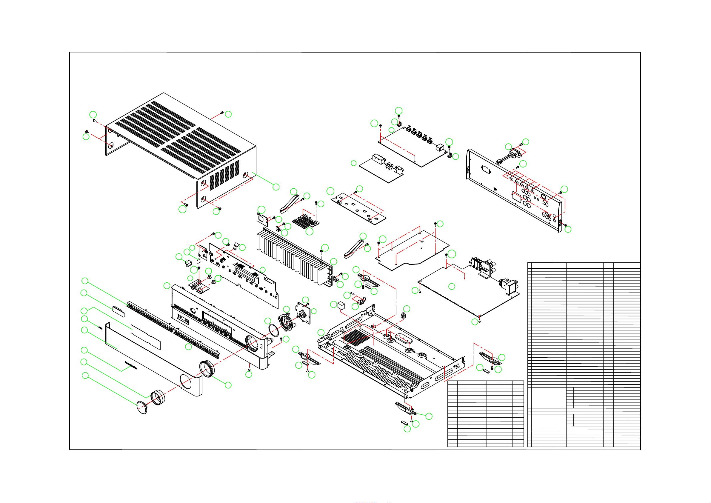
AVR151/230 EXPLODE VIEW
Harman Kardon
AVR151, AVR151S
Service Manual
Page 14 of 131
CTB4+10JFZR
S4
S3
8
7
6
5
4
3
2
1
CTB4+10JFZR
CTW3+8JR
11
12
S14
13
40-4
9
40-2
S11
S3
S3
S3
S5
S5
S1
10
33
S1
42-3
40-1
14
30
S6
31
15
S1
S6
25
16
18
S6
42-2
S5
S8
40-3
S6
19
S13
42-4
22
32
31
S6
S10
40-5
17
S8
20
S6
25
S6
S11
18
S11
S6
28
41
S6
S1
37
28
S2
S9
S7
S6
S7
Q,ty
1
1
1
1
111
1
1
1
1
1
11
11SHEET,BLIND CPE1A009
1
1
2
2
1
11
1
1
2CUSHION , RUBBER CHG1A160Z
1
1
1
1
1
1
11
11
11
11
11
1
1
REMARK
21
18
S6
S8
17
42-1
S6
18
DESCRIPTION PARTS NO. Q,ty
NO
S1
SCREW
S2
SCREW
S3
S4
SCREW
SCREW
S5
SCREW CTB3+8JR 4
S6
SCREW
S7
S8
SCREW
S9
SCREW CTB3+6JR 2
S10
SCREW CTW3+8JR 5
S11
SCREW
S12
SCREW 5
S13
SCREW CTB4+10JFZR 2
S14
CTB3+10JFZR
CTWS3+10GR
CTB4+6FFZR
CTB3+10JR
CTW3+12JR
CTS3+8JFZRSCREW 4
CTB3+6FFZR
CHD1A012R
CHD4A012R
S8
16
DESCRIPTION
NO
KNOB,VOLUME CBN1A269B65 1
1
INDICATOR,VOLUME
2
BADGE, HARMAN/KARDON
3
WINDOW,FIP CGU2A410A25J
4
BADGE,AVR151 CGB1A259Z
5
FILTER,FIP CMZ1A145
6
JACK,COVER CGR1A555B63
7
KNOB,STANDBY CBT2A1064
8
KNOB,BACK CBT2A1065
9
ORNAMENT,RING CGR1A538G5
10
PANEL,FRONT
11
INDICATOR,POWER CGL1A265Y
12
13
SHEET , VOLUME CGX1A476Z
14
HOLDER , LED CMH3A215
15
16
FOOT A
17
FOOT B
18
CUSHION , FOOT CHG1A373 4
CHASSIS,BOTTOM
19
COVER , SCREW CMD1A815 1
20
HOLDER , PCB CHE170 4
21
HEAT SINK CMY1A388
22
23
24
BRACKET , PCB CMD1A810 2
25
26
27
BRACKET,HDMI CMD1A809 2
28
PANEL,REAR CKF4A463Z 1
29
CABINET,TOP
30
31
BRACKET,H/S
32
PLATE , EARTH TOP CMC1A416 2
33
34
35
36
37
38
39
FRONT PCB ASS'Y
40
17CTB3+8JFZRSCREW
9
2
4
23
2
DIGITAL PCB ASS'Y COP12503H 11
41
MAIN PCB ASS'Y COP12506H 1
42
8
15
43
44
SMPS PCB ASS'Y
CGL1A300
CGB1A255Z
CGW1A533RHXB63
CKL1A094
CKL1A095
CUA1A343
CKC1A219B64
CMD1A802 2
COP12502H
40-1
40-2
40-3
40-4
40-5
42-1
42-2
42-3
42-4
COP12509B
PARTS NO.
FIP & KEY PCB
POWER LED PCB
VOLUME PCB
PHONE PCB
JACK PCB ASS'Y 1
MAIN PCB
GUIDE PCB(CARD)
GUIDE PCB(CARD)
SHIELD PCB
Page 15
Level Ref# Component Description Drawing No REQ-Qty
CGWAVR151/230
...3 CGB1A255Z BADGE , HARMAN/KARDON 1
...3 CGB1A259Z BADGE , AVR151 1
...3 CGL1A265Y INDICATOR , POWER AVR155 1
CGU2A410A25J
CGW1A533RHXB63
......6 C311 CCUS1H102KC CAP, CHIP(1608, 50V/1000pF) 1
......6 C322 CCUS1H102KC CAP, CHIP(1608, 50V/1000pF) 1
......6 C351 CCUS1H181JA CAP, CHIP(1608, 50V/180pF) 1608 SIZE 1
......6 C423 CCUS1H680JA CAP, CHIP(1608, 50V/68pF) 1
......6 C431 CCUS1H104KC CAP, CHIP(1608, 50V/0.1uF) 1
......6 C441 CCUS1H223KC CAP, CHIP(1608, 50V/0.022uF) 1
......6 C644 CCUS1H104KC CAP, CHIP(1608, 50V/0.1uF) 1
......6 C645 CCUS1H471JA CAP, CHIP(1608, 50V/470pF) 1
......6 C646 CCUS1H471JA CAP, CHIP(1608, 50V/470pF) 1
......6 C912 CCUS1H104KC CAP, CHIP(1608, 50V/0.1uF) 1
......6 C923 CCUS1H681JA CAP, CHIP(1608, 50V/680pF) 1
......6 C924 CCUS1H681JA CAP, CHIP(1608, 50V/680pF) 1
CVISN74ACT04DR
......6 IC421
HVINJM2244MTE1
I.C , VIDEO SWITCH QRW-6500 1
......6 IC91 HVTKTC812TB T.R , CHIP(TS 6) KTC812T-B-RTK/P 1
......6 IC92 HVTKTC812TB T.R , CHIP(TS 6) KTC812T-B-RTK/P 1
......6 Q721 CVTRT1N144C T.R,RT1N144C(10K-47K) RT1N144C 1
......6 Q906 CVTRT1P144C T.R,RT1P144C(10K-47K) RT1P144C-T112-1 1
Harman Kardon
AVR151, AVR151S
Service Manual
Service Manual
Page 15 of 131
..2 CBN1A269B65 KNOB , VOLUME 1
..2 CGL1A300 INDIC ATOR , VOLUME 1
..2 CGR1A555B63 COVER , JACK AVR1510 1
..2
...3 CBT2A1064 KNOB , STANDBY 1
...3 CBT2A1065 KNOB , BACK 1
...3 CGR1A538G5 ORNAMENT , RING 1
...3
...3
...3 CGX1A476Z SHEET , VOLUME 1
...3 CMC1A416 PLATE , EARTH TOP 2
...3 CMH3A215 HOLDER , LED 1
...3 CMZ1A145 FILTER AVR1510 1
...3 COP12502H AVR1510 FRONT PCB ASS'Y 1
......6 C109 CCUS1H104KC CAP, CHIP(1608, 50V/0.1uF) 1
......6 C121 CCUS1H151JA CAP, CHIP(1608, 50V/150pF) 1
......6 C151 CCUS1H104KC CAP, CHIP(1608, 50V/0.1uF) 1
......6 C213 CCUS1H223KC CAP, CHIP(1608, 50V/0.022uF) 1
......6 C214 CCUS1H223KC CAP, CHIP(1608, 50V/0.022uF) 1
......6 C352 CCUS1H104KC CAP, CHIP(1608, 50V/0.1uF) 1
......6 C361 CCUS1H103KC CAP, CHIP(1608, 50V/0.01uF) 1608 SIZE 1
......6 C362 CCUS1H103KC CAP, CHIP(1608, 50V/0.01uF) 1608 SIZE 1
......6 C363 CCUS1H104KC CAP, CHIP(1608, 50V/0.1uF) 1
......6 C364 CCUS1H104KC CAP, CHIP(1608, 50V/0.1uF) 1
......6 C365 CCUS1H104KC CAP, CHIP(1608, 50V/0.1uF) 1
......6 C366 CCUS1H104KC CAP, CHIP(1608, 50V/0.1uF) 1
......6 C421 CCUS1H104KC CAP, CHIP(1608, 50V/0.1uF) 1
......6 C422 CCUS1H104KC CAP, CHIP(1608, 50V/0.1uF) 1
......6 C442 CCUS1H223KC CAP, CHIP(1608, 50V/0.022uF) 1
......6 C451 CCUS1H104KC CAP, CHIP(1608, 50V/0.1uF) 1
......6 C456 CCUS1H104KC CAP, CHIP(1608, 50V/0.1uF) 1
......6 C557 CCUS1H104KC CAP, CHIP(1608, 50V/0.1uF) 1
......6 C558 CCUS1H104KC CAP, CHIP(1608, 50V/0.1uF) 1
......6 C601 CCUS1H104KC CAP, CHIP(1608, 50V/0.1uF) 1
......6 C602 CCUS1H104KC CAP, CHIP(1608, 50V/0.1uF) 1
......6 C603 CCUS1H104KC CAP, CHIP(1608, 50V/0.1uF) 1
......6 C604 CCUS1H104KC CAP, CHIP(1608, 50V/0.1uF) 1
......6 C605 CCUS1H104KC CAP, CHIP(1608, 50V/0.1uF) 1
AVR 151, 5.1CH RECEIVER, bill of materials
FRONT PANEL ASS'Y 1
WINDOW , FIP AVR170/230 1
PANEL , FRONT AVR1510 1
......6 C647 CCUS1H104KC CAP, CHIP(1608, 50V/0.1uF) 1
......6 C714 CCUS1H104KC CAP, CHIP(1608, 50V/0.1uF) 1
......6 C715 CCUS0J475KC CAP, CHIP(1608, 6.3V/4.7uF, MURATA GRM18) GRM188R60J475KE19D 1
......6 C732 CCUS1H104KC CAP, CHIP(1608, 50V/0.1uF) 1
......6 C751 CCUS1H222KC CAP, CHIP(1608, 50V/2200pF) 1
......6 C752 CCUS1H102KC CAP, CHIP(1608, 50V/1000pF) 1
......6 C753 CCUS1H102KC CAP, CHIP(1608, 50V/1000pF) 1
......6 C754 CCUS1H104KC CAP, CHIP(1608, 50V/0.1uF) 1
......6 C911 CCUS1H104KC CAP, CHIP(1608, 50V/0.1uF) 1
......6 C951 CCUS1H104KC CAP, CHIP(1608, 50V/0.1uF) 1
......6 C952 CCUS1H104KC CAP, CHIP(1608, 50V/0.1uF) 1
......6 D1 CVD1SS355T DIODE , CHIP , SWITCHING 1SS355(T/B) 1
......6 D2 CVD1SS355T DIODE , CHIP , SWITCHING 1SS355(T/B) 1
......6 D361 CVD1SS355T DIODE , CHIP , SWIT CHING 1SS355(T/B) 1
......6 D362 CVD1SS355T DIODE , CHIP , SWIT CHING 1SS355(T/B) 1
......6 D363 CVD1SS355T DIODE , CHIP , SWIT CHING 1SS355(T/B) 1
......6 D643 CVD1SS355T DIODE , CHIP , SWIT CHING 1SS355(T/B) 1
......6 D644 CVD1SS355T DIODE , CHIP , SWIT CHING 1SS355(T/B) 1
......6 IC13
......6 L451 HLZ9Z014Z CHIP , BEAD HU-1M4516-600JT 1
......6 Q111 CVTRT1P144C T.R,RT1P144C(10K-47K) RT1P144C-T112-1 1
......6 Q112 CVTRT1N144C T.R,RT1N144C(10K-47K) RT1N144C 1
......6 Q113 CVTRT1N144C T.R,RT1N144C(10K-47K) RT1N144C 1
......6 Q114 CVTRT1N144C T.R,RT1N144C(10K-47K) RT1N144C 1
......6 Q252 CVTRT1N144C T.R,RT1N144C(10K-47K) RT1N144C 1
......6 Q362 CVTRT1N141C T.R,RT1N141C(10K-10K) RT1N141C 1
......6 Q363 CVTRT1P141C T.R,RT1P141C(10K-10K) RT1P141C-T112-1 1
......6 Q373 CVTRT1P144C T.R,RT1P144C(10K-47K) RT1P144C-T112-1 1
......6 Q907 CVTRT1P144C T.R,RT1P144C(10K-47K) RT1P144C-T112-1 1
I.C , HEX INVERTERS(SO IC/D-14P) SN74ACT04DR 1
Page 16

Level Ref# Component Description Drawing No REQ-Qty
......6 R110 CRJ10DJ0R0T RES, CHIP(1608/5%/0ohm) 00200-0090 1
......6 R111 CRJ10DJ0R0T RES, CHIP(1608/5%/0ohm) 00200-0090 1
......6 R112 CRJ10DJ0R0T RES, CHIP(1608/5%/0ohm) 00200-0090 1
......6 R214 CRJ10DJ272T RES, CHIP(1608/5%/2.7Kohm) 1
......6 R251 CRJ10DJ222T RES, CHIP(1608/5%/2.2Kohm) 00200-0142 1
......6 R252 CRJ10DJ393T RES, CHIP(1608/5%/39Kohm) 1
......6 R327 CRJ10DF5601T RES, CHIP(1608/1%/5.6Kohm) 00200-0234 1
......6
R328 CRJ10DF5601T RES, CHIP(1608/1%/5.6Kohm) 00200-0234 1
......6 R351 CRJ10DJ750T RES, CHIP(1608/5%/75ohm) 1608 SIZE 1
......6 R375 CRJ10DJ103T RES, CHIP(1608/5%/10Kohm) 00200-0096 1
......6 R376 CRJ10DJ221T RES, CHIP(1608/5%/220ohm) 00200-0101 1
......6 R377 CRJ10DJ473T RES, CHIP(1608/5%/47Kohm) 00200-0185 1
......6 R432 CRJ10DJ100T RES, CHIP(1608/5%/10ohm) 1608 SIZE 1
......6 R451 CRJ10DJ472T RES, CHIP(1608/5%/4.7Kohm) 00200-0087 1
......6 R452 CRJ10DJ472T RES, CHIP(1608/5%/4.7Kohm) 00200-0087 1
......6 R605 CRJ10DJ103T RES, CHIP(1608/5%/10Kohm) 00200-0096 1
......6 R641 CRJ10DJ0R0T RES, CHIP(1608/5%/0ohm) 00200-0090 1
......6 R643 CRJ10DJ0R0T RES, CHIP(1608/5%/0ohm) 00200-0090 1
......6 R735 CRJ10DJ152T RES, CHIP(1608/5%/1.5Kohm) 00200-0119 1
......6 R741 CRJ10DJ123T RES, CHIP(1608/5%/12Kohm) 1608 SIZE 1
......6 R742 CRJ10DJ102T RES, CHIP(1608/5%/1Kohm) 00200-0094 1
Harman Kardon
AVR151, AVR151S
Service Manual
Service Manual
Page 16 of 131
...3 COP12502H AVR1510 FRONT PCB ASS'Y 1
......6 R101 CRJ10DJ221T RES, CHIP(1608/5%/220ohm) 00200-0101 1
......6 R102 CRJ10DJ681T RES, CHIP(1608/5%/680ohm) 00200-0120 1
......6 R104 CRJ10DJ103T RES, CHIP(1608/5%/10Kohm) 00200-0096 1
......6 R108 CRJ10DJ0R0T RES, CHIP(1608/5%/0ohm) 00200-0090 1
......6 R109 CRJ10DJ0R0T RES, CHIP(1608/5%/0ohm) 00200-0090 1
......6 R113 CRJ10DJ0R0T RES, CHIP(1608/5%/0ohm) 00200-0090 1
......6 R114 CRJ10DJ0R0T RES, CHIP(1608/5%/0ohm) 00200-0090 1
......6 R122 CRJ10DJ100T RES, CHIP(1608/5%/10ohm) 1608 SIZE 1
......6 R151 CRJ10DJ0R0T RES, CHIP(1608/5%/0ohm) 00200-0090 1
......6 R201 CRJ10DJ101T RES, CHIP(1608/5%/100ohm) 00200-0100 1
......6 R202 CRJ10DJ101T RES, CHIP(1608/5%/100ohm) 00200-0100 1
......6 R203 CRJ10DJ101T RES, CHIP(1608/5%/100ohm) 00200-0100 1
......6 R211 CRJ10DJ101T RES, CHIP(1608/5%/100ohm) 00200-0100 1
......6 R213 CRJ10DJ272T RES, CHIP(1608/5%/2.7Kohm) 1
......6 R312 CRJ10DF1001T RES, CHIP(1608/1%/1Kohm) RM06FB1K 1
......6 R313 CRJ10DF1501T RES, CHIP(1608/1%/1.5Kohm) 1.5K /1/10W/F 1
......6 R314 CRJ10DF1801T RES, CHIP(1608/1%/1.8Kohm) 1.8K /1/10W/F 1
......6 R315 CRJ10DF2701T RES, CHIP(1608/1%/2.7Kohm) RM06FB2K7 1
......6 R316 CRJ10DF3301T RES, CHIP(1608/1%/3.3Kohm) 1
......6 R322 CRJ10DF1001T RES, CHIP(1608/1%/1Kohm) RM06FB1K 1
......6 R323 CRJ10DF1501T RES, CHIP(1608/1%/1.5Kohm) 1.5K /1/10W/F 1
......6 R324 CRJ10DF1801T RES, CHIP(1608/1%/1.8Kohm) 1.8K /1/10W/F 1
......6 R325 CRJ10DF2701T RES, CHIP(1608/1%/2.7Kohm) RM06FB2K7 1
......6 R326 CRJ10DF3301T RES, CHIP(1608/1%/3.3Kohm) 1
......6 R352 CRJ10DJ103T RES, CHIP(1608/5%/10Kohm) 00200-0096 1
......6 R361 CRJ10DJ1R0T RES, CHIP(1608/5%/1ohm) 1608 SIZE 1
......6 R362 CRJ10DJ1R0T RES, CHIP(1608/5%/1ohm) 1608 SIZE 1
......6 R363 CRJ10DJ103T RES, CHIP(1608/5%/10Kohm) 00200-0096 1
......6 R364 CRJ10DJ4R7T RES, CHIP(1608/5%/4.7ohm) 00200-0099 1
......6 R365 CRJ10DJ4R7T RES, CHIP(1608/5%/4.7ohm) 00200-0099 1
......6 R366 CRJ10DJ103T RES, CHIP(1608/5%/10Kohm) 00200-0096 1
......6 R367 CRJ10DJ0R0T RES, CHIP(1608/5%/0ohm) 00200-0090 1
......6 R368 CRJ10DJ102T RES, CHIP(1608/5%/1Kohm) 00200-0094 1
AVR 151, 5.1CH RECEIVER, bill of materials
......6 R402 CRJ14CJ4R7T RES, CHIP(3216/5%/4.7ohm) 3216 1
......6 R404 CRJ14CJ4R7T RES, CHIP(3216/5%/4.7ohm) 3216 1
......6 R413 CRJ10DJ0R0T RES, CHIP(1608/5%/0ohm) 00200-0090 1
......6 R421 CRJ10DJ105T RES, CHIP(1608/5%/1Mohm) 00200-0095 1
......6 R422 CRJ10DJ105T RES, CHIP(1608/5%/1Mohm) 00200-0095 1
......6 R423 CRJ10DJ105T RES, CHIP(1608/5%/1Mohm) 00200-0095 1
......6 R424 CRJ10DJ0R0T RES, CHIP(1608/5%/0ohm) 00200-0090 1
......6 R425 CRJ10DJ101T RES, CHIP(1608/5%/100ohm) 00200-0100 1
......6 R426 CRJ10DJ101T RES, CHIP(1608/5%/100ohm) 00200-0100 1
......6 R431 CRJ10DJ100T RES, CHIP(1608/5%/10ohm) 1608 SIZE 1
......6 R453 CRJ10DJ472T RES, CHIP(1608/5%/4.7Kohm) 00200-0087 1
......6 R454 CRJ10DJ472T RES, CHIP(1608/5%/4.7Kohm) 00200-0087 1
......6 R455 CRJ14CJ101T RES, CHIP(3216/5%/100ohm) 3216 1
......6 R456 CRJ14CJ101T RES, CHIP(3216/5%/100ohm) 3216 1
......6 R457 CRJ10DJ103T RES, CHIP(1608/5%/10Kohm) 00200-0096 1
......6 R601 CRJ10DJ103T RES, CHIP(1608/5%/10Kohm) 00200-0096 1
......6 R602 CRJ10DJ103T RES, CHIP(1608/5%/10Kohm) 00200-0096 1
......6 R603 CRJ10DJ103T RES, CHIP(1608/5%/10Kohm) 00200-0096 1
......6 R604 CRJ10DJ103T RES, CHIP(1608/5%/10Kohm) 00200-0096 1
......6 R644 CRJ10DJ0R0T RES, CHIP(1608/5%/0ohm) 00200-0090 1
......6 R701 CRJ10DJ102T RES, CHIP(1608/5%/1Kohm) 00200-0094 1
......6 R702 CRJ10DJ102T RES, CHIP(1608/5%/1Kohm) 00200-0094 1
......6 R703 CRJ10DJ102T RES, CHIP(1608/5%/1Kohm) 00200-0094 1
......6 R711 CRJ10DJ470T RES, CHIP(1608/5%/47ohm) 00200-0098 1
......6 R712 CRJ10DJ470T RES, CHIP(1608/5%/47ohm) 00200-0098 1
......6 R713 CRJ10DJ470T RES, CHIP(1608/5%/47ohm) 00200-0098 1
......6 R721 CRJ10DJ103T RES, CHIP(1608/5%/10Kohm) 00200-0096 1
......6 R722 CRJ10DJ101T RES, CHIP(1608/5%/100ohm) 00200-0100 1
......6 R731 CRJ10DJ100T RES, CHIP(1608/5%/10ohm) 1608 SIZE 1
......6 R901 CRJ10DJ101T RES, CHIP(1608/5%/100ohm) 00200-0100 1
......6 R902 CRJ10DJ101T RES, CHIP(1608/5%/100ohm) 00200-0100 1
......6 R921 CRJ10DJ102T RES, CHIP(1608/5%/1Kohm) 00200-0094 1
......6 R922 CRJ10DJ102T RES, CHIP(1608/5%/1Kohm) 00200-0094 1
Page 17

Level Ref# Component Description Drawing No REQ-Qty
......6 R932 CRJ10DJ104T RES, CHIP(1608/5%/100Kohm) 00200-0097 1
......6 R933 CRJ10DJ221T RES, CHIP(1608/5%/220ohm) 00200-0101 1
......6 R934 CRJ10DJ221T RES, CHIP(1608/5%/220ohm) 00200-0101 1
HVDUDZS5.6BSR
......6 ZD452
HVDUDZS5.6BSR
DIODE , ZENER(CHIP,5.6V) UDZSTE-175.6B 1
......6 ZD453
HVDUDZS5.6BSR
DIODE , ZENER(CHIP,5.6V) UDZSTE-175.6B 1
.....5 C108
CCEA1AH471TC
CAP, ELECT(10V/470uF) 1
CCEA1AKS331TC
CCEA1HH100TC
CCEA1CH101TC
CCEA1HKS2R2TC
CCEA1HH470TC
CCEA1AH471TC
CCEA1HH100TC
CCEA1HH100TC
CCEA1CH101TC
CCEA1JH470TCS
.....5 C454
CCME2E273JX14T
CAP , POLYESTER FILM(250V/0.027UF, 5%) 1
.....5
C455
CCEA1CH101TC
CAP, ELECT(16V/100uF) 1
.....5 C556
CCEA1AKS331TC
CAP, ELECT(10V/330uF)-S 1
CCEA1AKS331TC
CCEA1HKS2R2TC
CCEA1AH471TC
CCEA1HH100TC
CCEA1HH100TC
CCEA1CH331TC
CCEA1CH331TC
CCEA1VKS470TCS
CCEA1VKS470TCS
.....5 ET90 CJT1A026 PLATE , EARTH(TRONIC ELECTRONICS) 1
.....5 L452 CLZ9Z112Z COIL , CHOKE ( 220uH ) 1
.....5 Q251
HVTKTA1271YT
T.R KTA1271-Y-AT/P 1
HVTKTA1266YT
.....5 S318 CST1A024ZT SW , TACT 1
.....5 S319 CST1A024ZT SW , TACT 1
.....5 S320 CST1A024ZT SW , TACT 1
CMD1A572-V1
CMD1A572-V1
CWB1B007150HC
CWB1B005100HC
....4 BN73 CJP06GB142ZB PIN HEADER(6P, 2.54mm) 1
....4 BN76
CWB1C207380H6001
WIRE ASS'Y (7P,2.0mm,380mm,Shield_ANGLE)_usb 1
....4 BN78
CWB1B005100HC
WIRE ASS'Y Locking (YH) (5P,2MM,100MM,26#) 1
CVD1L0345W31BOCT201V
CVD30ASOGCAA-S7
CVD1L0345W31BOCT201V
CVD1L0345W31BOCT201V
CVD1L0345W31BOCT201V
CFL162SD19GINK
CRVKSM603TE5B
....4 IC15
HVINJM4556AL
I.C , HEADPHONE (JRC) NJM4556AL 1
....4 IC371 BVIKP1010B IC, PHOTO COUPLER (COSMO) 1
....4 JK351 CJJ4M044X JACK , RCA (1P,RCA-115A-04) RCA-115A-04 1
Harman Kardon
AVR151, AVR151S
Service ManualService Manual
Page 17 of 131
...3 COP12502H AVR1510 FRONT PCB ASS'Y 1
......6 R923 CRJ10DJ152T RES, CHIP(1608/5%/1.5Kohm) 00200-0119 1
......6 R924 CRJ10DJ152T RES, CHIP(1608/5%/1.5Kohm) 00200-0119 1
......6 R925 CRJ10DJ104T RES, CHIP(1608/5%/100Kohm) 00200-0097 1
......6 R926 CRJ10DJ104T RES, CHIP(1608/5%/100Kohm) 00200-0097 1
......6 R931 CRJ10DJ104T RES, CHIP(1608/5%/100Kohm) 00200-0097 1
......6 R935 CRJ10DJ221T RES, CHIP(1608/5%/220ohm) 00200-0101 1
......6 R936 CRJ10DJ221T RES, CHIP(1608/5%/220ohm) 00200-0101 1
......6 R941 CRJ10DJ472T RES, CHIP(1608/5%/4.7Kohm) 00200-0087 1
......6 R942 CRJ10DJ472T RES, CHIP(1608/5%/4.7Kohm) 00200-0087 1
......6 R943 CRJ10DJ472T RES, CHIP(1608/5%/4.7Kohm) 00200-0087 1
......6 R944 CRJ10DJ472T RES, CHIP(1608/5%/4.7Kohm) 00200-0087 1
......6 R951 CRJ10DJ0R0T RES, CHIP(1608/5%/0ohm) 00200-0090 1
......6 R952 CRJ10DJ0R0T RES, CHIP(1608/5%/0ohm) 00200-0090 1
......6 ZD451
AVR 151, 5.1CH RECEIVER, bill of materials
DIODE , ZENER(CHIP,5.6V) UDZSTE-175.6B 1
.....5 C122
.....5 C152
.....5 C251
.....5 C252
.....5 C401
.....5 C424
.....5 C425
.....5 C426
.....5 C452
.....5 C453
.....5 C559
.....5 C721
.....5 C731
.....5 C901
.....5 C902
.....5 C931
.....5 C932
.....5 C933
.....5 C944
.....5 Q361
.....5 Q451 CVTKTC1027YT T.R KTC1027Y 1
.....5 Q452 CVTKTC1027YT T.R KTC1027Y 1
.....5 S311 CST1A024ZT SW , TACT 1
.....5 S312 CST1A024ZT SW , TACT 1
.....5 S313 CST1A024ZT SW , TACT 1
.....5 S314 CST1A024ZT SW , TACT 1
.....5 S315 CST1A024ZT SW , TACT 1
.....5 S316 CST1A024ZT SW , TACT 1
.....5 S317 CST1A024ZT SW , TACT 1
.....5 S321 CST1A024ZT SW , TACT 1
.....5 S322 CST1A024ZT SW , TACT 1
.....5 S323 CST1A024ZT SW , TACT 1
.....5 S330 CST1A024ZT SW , TACT 1
....4 BK30 CMD1A775 BRACKET, SHIELD 1
....4 BK71
....4 BK72
....4 BN71
....4 BN72
CAP, ELECT(10V/330uF)-S 1
CAP, ELECT(50V/10uF) 1
CAP, ELECT(16V/100uF) 1
CAP, ELECT(50V/2.2uF)-S 1
CAP , ELECT (50V/47uF) 1
CAP, ELECT(10V/470uF) 1
CAP, ELECT(50V/10uF) 1
CAP, ELECT(50V/10uF) 1
CAP, ELECT(16V/100uF) 1
CAP , ELECT(63V/47uF),105'C 1
CAP, ELECT(10V/330uF)-S 1
CAP, ELECT(50V/2.2uF)-S 1
CAP, ELECT(10V/470uF) 1
CAP, ELECT(50V/10uF) 1
CAP, ELECT(50V/10uF) 1
CAP, ELECT(16V/330uF) 1
CAP, ELECT(16V/330uF) 1
CAP, ELECT(35V/47uF, 105'C)-S 1
CAP, ELECT(35V/47uF, 105'C)-S 1
T.R KTA1266-Y-AT/PJ 1
BRACKET , FIP 1
BRACKET , FIP 1
WIRE ASS'Y Locking (YH) (7P,2MM,150MM,#26) 1
WIRE ASS'Y Locking (YH) (5P,2MM,100MM,26#) 1
....4 CN72 CJP05GJ288ZY LOCK-WAFER/ANGLE/2MM PITCH/5PIN 1
....4 CN73 CJP06GB143ZB FEMALE HEADER(6P, 2.54mm) 1
....4 CN78 CJP05GI236ZW LOCKING TYPE , STRAIGHT WAFER , 2mm A2008WV0-5P 1
....4 D101
....4 D102
....4 D201
....4 D202
....4 D203
....4 FIP1
....4 IC12
....4 JK352 CJSJSR1124 MODUL E , OPTICAL(RX 16MHz) 1
....4 JK401 CJJ4S010Z JACK , BOARD RCA-325A-02 1
....4 JK402 CJJ2D008Z JACK, STEREO (BLK MOLD) PJ-308-02 1
....4 JK403 CJJ2D008Z JACK, STEREO (BLK MOLD) PJ-308-02 1
L.E.D , WHITE 1
L.E.D , ORANGE 1
L.E.D , WHITE 1
L.E.D , WHITE 1
L.E.D , WHITE 1
V.F.D , (FUTABA, 162-SD-19GINK) 162SD19GINK 1
SENSOR , REMOCO N 1
Page 18
Level Ref# Component Description Drawing No REQ-Qty
CWE8202150RV
CWE8202120RV
CWE5202080A
....4 TF94 CLT9Z092ZE TRANS , DC-AC (AVR1X1) 1
....4 VR74 CSR2A037Z ENCODER 1
....4 WF31
CJP11GA285ZN
WAFER, FFC(11P-1.25mm, STRAIGHT) 1
CJP23GA285ZN
CWC6C4A23B220B10
..2 CTB4+10JFZR SCREW 2
..2 CTB4+6FFZR SCREW 4
..2
CUAAVR151/230
BOTTOM CHASSIS ASS'Y 1
.......7 C1008 CCUC0J106KC CAP, CHIP(2012, 6.3V /10uF, X7R) LAO-63V103MS56PW# 1
.......7
C1009 CCUI1C104KC CAP, CHIP(1005, 16V/0.1uF) 1
.......7 C1010 CCUI1E103KC CAP, CHIP(1005, 25V/0.01uF) 0402B103K250HI 1
.......7 C1020 CCUC0J106KC CAP, CHIP(2012, 6.3V /10uF, X7R) LAO-63V103MS56PW# 1
.......7 C1021 CCUI1C104KC CAP, CHIP(1005, 16V/0.1uF) 1
.......7 C1022 CCUI1E103KC CAP, CHIP(1005, 25V/0.01uF) 0402B103K250HI 1
.......7 C1033 CCUC0J106KC CAP, CHIP(2012, 6.3V /10uF, X7R) LAO-63V103MS56PW# 1
.......7 C1034 CCUI1C104KC CAP, CHIP(1005, 16V/0.1uF) 1
.......7 C1035 CCUI1E103KC CAP, CHIP(1005, 25V/0.01uF) 0402B103K250HI 1
.......7 C1045 CCUC0J106KC CAP, CHIP(2012, 6.3V /10uF, X7R) LAO-63V103MS56PW# 1
.......7 C1046 CCUI1C104KC CAP, CHIP(1005, 16V/0.1uF) 1
.......7 C1047 CCUI1C104KC CAP, CHIP(1005, 16V/0.1uF) 1
.......7 C1119 CCUC0J106KC CAP, CHIP(2012, 6.3V /10uF, X7R) LAO-63V103MS56PW# 1
.......7 C1120 CCUS1H222KC CAP, CHIP(1608, 50V/2200pF) 1
.......7 C1121 CCUS1H222KC CAP, CHIP(1608, 50V/2200pF) 1
Harman Kardon
AVR151, AVR151S
Service ManualService Manual
Page 18 of 131
...3 COP12502H AVR1510 FRONT PCB ASS'Y 1
....4 JK53 CJJ9X012Z JACK , USB (ANGLE TYPE) 1
....4 JK64 CJJ2E026Z JACK, PHONES(6.35mm,SILVER) PJ-612A-51 1
....4 JW19
....4 JW20
....4 JW21
AVR 151, 5.1CH RECEIVER, bill of materials
WIRE ASS'Y HTS-5000 1
WIRE ASS'Y PM-4200 1
WIRE ASS'Y (1P, 80MM,BLK,#22) 1
....4 WF70
...3 CPE1A009 SHEET , BLIND 1
...3 CTB3+10JR SCREW 28
...3 CTWS3+10GR SCREW 2
...3
..2 CKC1A219B64 CABINET, TOP AVR1510 1
..2 CQB1A549Y LABEL , ATTENTION DVD48 1
..2 CQB1A622 LABEL , SERIAL NO DVD-310 1
..2 CTB3+8JFZR SCREW 15
...3 CHD4A012R SCREW , SPECIAL 4
...3 CHE170 HOLD ER , PCB ALL MODEL 4
...3 CHG1A373 CUSHION , FOOT AVR350 4
...3 CHS1A032 TAPE , HEMELON 4
...3 CKF4A463Z PANEL , REAR AVR151 1
...3 CKL1A094 FOOT , A AVR350 2
...3 CKL1A095 FOOT , B AVR350 2
...3 CMD1A809 BRAC KET , HDMI 2
...3 CMD1A815 CO VER , SCREW 1
...3 COP12503I AVR151/230 DIGITAL PCB ASS'Y (EUR) 1
.......7 C1011 CCUI1C104KC CAP, CHIP(1005, 16V/0.1uF) 1
.......7 C1012 CCUI1E103KC CAP, CHIP(1005, 25V/0.01uF) 0402B103K250HI 1
.......7 C1013 CCUI1C104KC CAP, CHIP(1005, 16V/0.1uF) 1
.......7 C1014 CCUC0J106KC CAP, CHIP(2012, 6.3V/10uF, X7R) LAO-63V103MS56PW# 1
.......7 C1015 CCUI1C104KC CAP, CHIP(1005, 16V/0.1uF) 1
.......7 C1016 CCUI1E103KC CAP, CHIP(1005, 25V/0.01uF) 0402B103K250HI 1
.......7 C1017 CCUI1C104KC CAP, CHIP(1005, 16V/0.1uF) 1
.......7 C1018 CCUI1E103KC CAP, CHIP(1005, 25V/0.01uF) 0402B103K250HI 1
.......7 C1019 CCUI1C104KC CAP, CHIP(1005, 16V/0.1uF) 1
.......7 C1023 CCUI1C104KC CAP, CHIP(1005, 16V/0.1uF) 1
.......7 C1024 CCUI1E103KC CAP, CHIP(1005, 25V/0.01uF) 0402B103K250HI 1
.......7 C1025 CCUC0J106KC CAP, CHIP(2012, 6.3V/10uF, X7R) LAO-63V103MS56PW# 1
.......7 C1026 CCUI1C104KC CAP, CHIP(1005, 16V/0.1uF) 1
.......7 C1027 CCUI1E103KC CAP, CHIP(1005, 25V/0.01uF) 0402B103K250HI 1
.......7 C1028 CCUC0J106KC CAP, CHIP(2012, 6.3V/10uF, X7R) LAO-63V103MS56PW# 1
.......7 C1029 CCUI1C104KC CAP, CHIP(1005, 16V/0.1uF) 1
.......7 C1030 CCUI1E103KC CAP, CHIP(1005, 25V/0.01uF) 0402B103K250HI 1
.......7 C1031 CCUI1C104KC CAP, CHIP(1005, 16V/0.1uF) 1
.......7 C1032 CCUI1E103KC CAP, CHIP(1005, 25V/0.01uF) 0402B103K250HI 1
WAFER,FPC 1.25mm,stright 1
CARD , CABLE (23P,1.25mm,220mm,B,10mm) 1
.......7 C1036 CCUC0J106KC CAP, CHIP(2012, 6.3V/10uF, X7R) LAO-63V103MS56PW# 1
.......7 C1037 CCUI1C104KC CAP, CHIP(1005, 16V/0.1uF) 1
.......7 C1038 CCUI1E103KC CAP, CHIP(1005, 25V/0.01uF) 0402B103K250HI 1
.......7 C1039 CCUI1C104KC CAP, CHIP(1005, 16V/0.1uF) 1
.......7 C1040 CCUI1E103KC CAP, CHIP(1005, 25V/0.01uF) 0402B103K250HI 1
.......7 C1041 CCUI1C104KC CAP, CHIP(1005, 16V/0.1uF) 1
.......7 C1042 CCUI1E103KC CAP, CHIP(1005, 25V/0.01uF) 0402B103K250HI 1
.......7 C1043 CCUI1C104KC CAP, CHIP(1005, 16V/0.1uF) 1
.......7 C1044 CCUI1E103KC CAP, CHIP(1005, 25V/0.01uF) 0402B103K250HI 1
.......7 C1048 CCUI1C104KC CAP, CHIP(1005, 16V/0.1uF) 1
.......7 C1049 CCUI1C104KC CAP, CHIP(1005, 16V/0.1uF) 1
.......7 C1053 CCUS1A105KC CAP, CHIP(1608, 10V/1uF) 1
.......7 C1054 CCUS1A105KC CAP, CHIP(1608, 10V/1uF) 1
.......7 C1101 CCUC1A226KC CAP, CHIP(2012, 10V/22uF) 1
.......7 C1102 CCUS1H103KC CAP, CHIP(1608, 50V/0.01uF) 1608 SIZE 1
.......7 C1105 CCUI1C104KC CAP, CHIP(1005, 16V/0.1uF) 1
.......7 C1108 CCUS1H104KC CAP, CHIP(1608, 50V/0.1uF) 1
.......7 C1113 CCUS1H104KC CAP, CHIP(1608, 50V/0.1uF) 1
.......7 C1114 CCUS1H104KC CAP, CHIP(1608, 50V/0.1uF) 1
.......7 C1130 CCUS1H104KC CAP, CHIP(1608, 50V/0.1uF) 1
.......7 C1132 CCUP0J226KC CAP, CHIP(3216, 6.3V/22uF) 1
.......7 C1134 CCUS1H103KC CAP, CHIP(1608, 50V/0.01uF) 1608 SIZE 1
.......7 C1137 CCUS1A105KC CAP, CHIP(1608, 10V/1uF) 1
Page 19

Level Ref# Component Description Drawing No REQ-Qty
.......7 C1149 CCUS1H680JA CAP, CHIP(1608, 50V/68pF) 1
.......7 C1150 CCUS1H103KC CAP, CHIP(1608, 50V/0.01uF) 1608 SIZE 1
.......7 C1151 CCUS1H104KC CAP, CHIP(1608, 50V/0.1uF) 1
.......7 C1167 CCUS1H680JA CAP, CHIP(1608, 50V/68pF) 1
.......7 C1168 CCUS1H103KC CAP, CHIP(1608, 50V/0.01uF) 1608 SIZE 1
.......7 C1169 CCUS1H104KC CAP, CHIP(1608, 50V/0.1uF) 1
.......7 C1215 CCUS1H104KC CAP, CHIP(1608, 50V/0.1uF) 1
.......7
C1222 CCUC1A226KC CAP, CHIP(2012, 10V/22uF) 1
.......7 C1233 CCUC1A226KC CAP, CHIP(2012, 10V/22uF) 1
.......7 C1308 CCUS1H101JA CAP, CHIP(1608, 50V/100pF) 1
.......7 C1309 CCUS1H272KC CAP, CHIP(1608, 50V/2700pF) 1
.......7 C1310 CCUS1H104KC CAP, CHIP(1608, 50V/0.1uF) 1
.......7 C1326 CCUS1H223KC CAP, CHIP(1608, 50V/0.022uF) 1
.......7 C1327 CCUS1H104KC CAP, CHIP(1608, 50V/0.1uF) 1
.......7 C1328 CCUC1A226KC CAP, CHIP(2012, 10V/22uF) 1
.......7 C1358 CCUS1H104KC CAP, CHIP(1608, 50V/0.1uF) 1
.......7 C1359 CCUS1H104KC CAP, CHIP(1608, 50V/0.1uF) 1
.......7 C1360 CCUS1H104KC CAP, CHIP(1608, 50V/0.1uF) 1
.......7 C1372 CCUS1H104KC CAP, CHIP(1608, 50V/0.1uF) 1
.......7 C1373 CCUS1H104KC CAP, CHIP(1608, 50V/0.1uF) 1
.......7 C1374 CCUS1H104KC CAP, CHIP(1608, 50V/0.1uF) 1
Harman Kardon
AVR151, AVR151S
Service ManualService Manual
Page 19 of 131
...3 COP12502H AVR1510 FRONT PCB ASS'Y 1
.......7 C1140 CCUS1H103KC CAP, CHIP(1608, 50V/0.01uF) 1608 SIZE 1
.......7 C1144 CCUS1H104KC CAP, CHIP(1608, 50V/0.1uF) 1
.......7 C1146 CCUS1A105KC CAP, CHIP(1608, 10V/1uF) 1
.......7 C1147 CCUS1H104KC CAP, CHIP(1608, 50V/0.1uF) 1
.......7 C1148 CCUS1A105KC CAP, CHIP(1608, 10V/1uF) 1
.......7 C1152 CCUS1H104KC CAP, CHIP(1608, 50V/0.1uF) 1
.......7 C1153 CCUS1H103KC CAP, CHIP(1608, 50V/0.01uF) 1608 SIZE 1
.......7 C1154 CCUS1H680JA CAP, CHIP(1608, 50V/68pF) 1
.......7 C1155 CCUS1H100JA CAP, CHIP(1608, 50V/10pF) 1
.......7 C1157 CCUS1H104KC CAP, CHIP(1608, 50V/0.1uF) 1
.......7 C1158 CCUS1A105KC CAP, CHIP(1608, 10V/1uF) 1
.......7 C1159 CCUS1H104KC CAP, CHIP(1608, 50V/0.1uF) 1
.......7 C1165 CCUS1H103KC CAP, CHIP(1608, 50V/0.01uF) 1608 SIZE 1
.......7 C1166 CCUS1H104KC CAP, CHIP(1608, 50V/0.1uF) 1
.......7 C1170 CCUS1H103KC CAP, CHIP(1608, 50V/0.01uF) 1608 SIZE 1
.......7 C1171 CCUS1H680JA CAP, CHIP(1608, 50V/68pF) 1
.......7 C1172 CCUS0J225KC CAP, CHIP(1608, 6.3V/2.2uF) 1
.......7 C1190 CCUS1H104KC CAP, CHIP(1608, 50V/0.1uF) 1
.......7 C1191 CCUS1H104KC CAP, CHIP(1608, 50V/0.1uF) 1
.......7 C1202 CCUS1H104KC CAP, CHIP(1608, 50V/0.1uF) 1
.......7 C1204 CCUS1H104KC CAP, CHIP(1608, 50V/0.1uF) 1
.......7 C1206 CCUS1H104KC CAP, CHIP(1608, 50V/0.1uF) 1
.......7 C1212 CCUS1H104KC CAP, CHIP(1608, 50V/0.1uF) 1
.......7 C1213 CCUS1H103KC CAP, CHIP(1608, 50V/0.01uF) 1608 SIZE 1
.......7 C1241 CCUS1H104KC CAP, CHIP(1608, 50V/0.1uF) 1
.......7 C1244 CCUC1A226KC CAP, CHIP(2012, 10V/22uF) 1
.......7 C1245 CCUS1H104KC CAP, CHIP(1608, 50V/0.1uF) 1
.......7 C1248 CCUS1H104KC CAP, CHIP(1608, 50V/0.1uF) 1
.......7 C1301 CCUS1H101JA CAP, CHIP(1608, 50V/100pF) 1
.......7 C1302 CCUS1H272KC CAP, CHIP(1608, 50V/2700pF) 1
.......7 C1303 CCUS1H104KC CAP, CHIP(1608, 50V/0.1uF) 1
.......7 C1304 CCUS1H151JA CAP, CHIP(1608, 50V/150pF) 1
.......7 C1307 CCUS1H104KC CAP, CHIP(1608, 50V/0.1uF) 1
AVR 151, 5.1CH RECEIVER, bill of materials
.......7 C1311 CCUS1H151JA CAP, CHIP(1608, 50V/150pF) 1
.......7 C1313 CCUS1H104KC CAP, CHIP(1608, 50V/0.1uF) 1
.......7 C1314 CCUS1H102KC CAP, CHIP(1608, 50V/1000pF) 1
.......7 C1317 CCUC1A226KC CAP, CHIP(2012, 10V/22uF) 1
.......7 C1318 CCUS1H104KC CAP, CHIP(1608, 50V/0.1uF) 1
.......7 C1319 CCUS1H104KC CAP, CHIP(1608, 50V/0.1uF) 1
.......7 C1322 CCUS1H104KC CAP, CHIP(1608, 50V/0.1uF) 1
.......7 C1323 CCUS1H104KC CAP, CHIP(1608, 50V/0.1uF) 1
.......7 C1324 CCUC1A226KC CAP, CHIP(2012, 10V/22uF) 1
.......7 C1325 CCUS1H102KC CAP, CHIP(1608, 50V/1000pF) 1
.......7 C1329 CCUS1H103KC CAP, CHIP(1608, 50V/0.01uF) 1608 SIZE 1
.......7 C1330 CCUS1H103KC CAP, CHIP(1608, 50V/0.01uF) 1608 SIZE 1
.......7 C1331 CCUS1H103KC CAP, CHIP(1608, 50V/0.01uF) 1608 SIZE 1
.......7 C1333 CCUS1H103KC CAP, CHIP(1608, 50V/0.01uF) 1608 SIZE 1
.......7 C1350 CCUS1H104KC CAP, CHIP(1608, 50V/0.1uF) 1
.......7 C1351 CCUS1H104KC CAP, CHIP(1608, 50V/0.1uF) 1
.......7 C1354 CCUC1A226KC CAP, CHIP(2012, 10V/22uF) 1
.......7 C1355 CCUS1H104KC CAP, CHIP(1608, 50V/0.1uF) 1
.......7 C1357 CCUS1H104KC CAP, CHIP(1608, 50V/0.1uF) 1
.......7 C1361 CCUS1H104KC CAP, CHIP(1608, 50V/0.1uF) 1
.......7 C1362 CCUS1H104KC CAP, CHIP(1608, 50V/0.1uF) 1
.......7 C1364 CCUS1H104KC CAP, CHIP(1608, 50V/0.1uF) 1
.......7 C1365 CCUS1H104KC CAP, CHIP(1608, 50V/0.1uF) 1
.......7 C1366 CCUS1H104KC CAP, CHIP(1608, 50V/0.1uF) 1
.......7 C1367 CCUS1H104KC CAP, CHIP(1608, 50V/0.1uF) 1
.......7 C1368 CCUS1H104KC CAP, CHIP(1608, 50V/0.1uF) 1
.......7 C1369 CCUS1H104KC CAP, CHIP(1608, 50V/0.1uF) 1
.......7 C1370 CCUS1H104KC CAP, CHIP(1608, 50V/0.1uF) 1
.......7 C1371 CCUS1H104KC CAP, CHIP(1608, 50V/0.1uF) 1
.......7 C1375 CCUS1H104KC CAP, CHIP(1608, 50V/0.1uF) 1
.......7 C1376 CCUS1H104KC CAP, CHIP(1608, 50V/0.1uF) 1
.......7 C1377 CCUS1H104KC CAP, CHIP(1608, 50V/0.1uF) 1
.......7 C1378 CCUS1H104KC CAP, CHIP(1608, 50V/0.1uF) 1
Page 20

.......7 C1402 CCUS1H102KC CAP, CHIP(1608, 50V/1000pF) 1
.......7 C1403 CCUS1H102KC CAP, CHIP(1608, 50V/1000pF) 1
.......7 C1404 CCUS1H221JA CAP, CHIP(1608, 50V/220pF) 1
.......7 C1417 CCUS1H104KC CAP, CHIP(1608, 50V/0.1uF) 1
.......7 C1418 CCUS1H104KC CAP, CHIP(1608, 50V/0.1uF) 1
.......7 C1419 CCUS1H104KC CAP, CHIP(1608, 50V/0.1uF) 1
.......7 C1451 CCUC0J106KC CAP, CHIP(2012, 6.3V/10uF, X7R) LAO-63V103MS56PW# 1
.......7
C1456 CCUS1H103KC CAP, CHIP(1608, 50V/0.01uF) 1608 SIZE 1
.......7 C1457 CCUC1A225KC CAP, CHIP(2012, 10V/2.2uF) 1
.......7 C1523 CCUS1H391JA CAP, CHIP(1608, 50V/390pF) 1
.......7 C1527 CCUS1H103KC CAP, CHIP(1608, 50V/0.01uF) 1608 SIZE 1
.......7 C1528 CCUS1H103KC CAP, CHIP(1608, 50V/0.01uF) 1608 SIZE 1
.......7 D1401 CVDBAR43C DIODE, SCHOTTKY BA R43CFILM 1
.......7 D1402 CVD1SS355T D IODE , CHIP , SWITCHING 1SS355(T/B) 1
.......7 D1403 CVD1SS355T D IODE , CHIP , SWITCHING 1SS355(T/B) 1
HVDUDZS3.3BSR
CRTMINISMDC200F
CVIMFI337S3959-HK
CVIPCM5100PWR
CVIAT45DB321D-SU
HVINJM2115MDTE1
HVINJM2115MDTE1
.......7 IC1404
CVICAT24C32WI-GT3
I.C, EEPROM, 32K CAT24C32WI-GT3 1
.......7 IC1406
CVICAT809RTBI-GT3
I.C , RESET IC (2.63V, SOT-23-3) CAT809RTBI-GT3 1
.......7 L1001 CLZ9R005V FERRITE CHIP BEAD(1608/60R, CB03YTYH600) 1
.......7 L1116 CLZ9R005V FERRITE CHIP BEAD(1608/60R, CB03YTYH600) 1
.......7 L1117 CLZ9R005V FERRITE CHIP BEAD(1608/60R, CB03YTYH600) 1
.......7 L1118 CLZ9R005V FERRITE CHIP BEAD(1608/60R, CB03YTYH600) 1
Harman Kardon
AVR151, AVR151S
Service ManualService Manual
Page 20 of 131
Level Ref# Component Description Drawing No REQ-Qty
...3 COP12502H AVR1510 FRONT PCB ASS'Y 1
.......7 C1379 CCUS1H104KC CAP, CHIP(1608, 50V/0.1uF) 1
.......7 C1382 CCUS1H104KC CAP, CHIP(1608, 50V/0.1uF) 1
.......7 C1384 CCUS1H104KC CAP, CHIP(1608, 50V/0.1uF) 1
.......7 C1387 CCUS1H104KC CAP, CHIP(1608, 50V/0.1uF) 1
.......7 C1389 CCUS1H104KC CAP, CHIP(1608, 50V/0.1uF) 1
.......7 C1405 CCUS1H104KC CAP, CHIP(1608, 50V/0.1uF) 1
.......7 C1406 CCUS1H104KC CAP, CHIP(1608, 50V/0.1uF) 1
.......7 C1409 CCUS1H103KC CAP, CHIP(1608, 50V/0.01uF) 1608 SIZE 1
.......7 C1410 CCUC1A225KC CAP, CHIP(2012, 10V/2.2uF) 1
.......7 C1412 CCUC1A226KC CAP, CHIP(2012, 10V/22uF) 1
.......7 C1413 CCUS1H151JA CAP, CHIP(1608, 50V/150pF) 1
.......7 C1414 CCUS1H104KC CAP, CHIP(1608, 50V/0.1uF) 1
.......7 C1415 CCUS1H104KC CAP, CHIP(1608, 50V/0.1uF) 1
.......7 C1416 CCUS1H102KC CAP, CHIP(1608, 50V/1000pF) 1
.......7 C1420 CCUS1H104KC CAP, CHIP(1608, 50V/0.1uF) 1
.......7 C1421 CCUS1H104KC CAP, CHIP(1608, 50V/0.1uF) 1
.......7 C1422 CCUS1H104KC CAP, CHIP(1608, 50V/0.1uF) 1
.......7 C1423 CCUS1H104KC CAP, CHIP(1608, 50V/0.1uF) 1
.......7 C1424 CCUS1H104KC CAP, CHIP(1608, 50V/0.1uF) 1
.......7 C1425 CCUS1H104KC CAP, CHIP(1608, 50V/0.1uF) 1
.......7 C1426 CCUS1H104KC CAP, CHIP(1608, 50V/0.1uF) 1
.......7 C1427 CCUS1H104KC CAP, CHIP(1608, 50V/0.1uF) 1
.......7 C1430 CCUS0J475KC CAP, CHIP(1608, 6.3V/4.7uF, MURATA GRM18) GRM188R60J475KE19D 1
.......7 C1450 CCUS1H104KC CAP, CHIP(1608, 50V/0.1uF) 1
.......7 C1505 CCUS1H272KC CAP, CHIP(1608, 50V/2700pF) 1
.......7 C1506 CCUS1H272KC CAP, CHIP(1608, 50V/2700pF) 1
.......7 C1508 CCUS1H391JA CAP, CHIP(1608, 50V/390pF) 1
.......7 C1509 CCUS1H391JA CAP, CHIP(1608, 50V/390pF) 1
.......7 C1513 CCUS1H103KC CAP, CHIP(1608, 50V/0.01uF) 1608 SIZE 1
.......7 C1514 CCUS1H103KC CAP, CHIP(1608, 50V/0.01uF) 1608 SIZE 1
.......7 C1519 CCUS1H683KC CAP, CHIP(1608, 50V/0.068uF) 1
.......7 C1520 CCUS1H272KC CAP, CHIP(1608, 50V/2700pF) 1
.......7 C1522 CCUS1H822KC CAP, CHIP(1608, 50V/8200pF) 1
AVR 151, 5.1CH RECEIVER, bill of materials
.......7 C1533 CCUS1H272KC CAP, CHIP(1608, 50V/2700pF) 1
.......7 C1534 CCUS1H272KC CAP, CHIP(1608, 50V/2700pF) 1
.......7 C1536 CCUS1H391JA CAP, CHIP(1608, 50V/390pF) 1
.......7 C1537 CCUS1H391JA CAP, CHIP(1608, 50V/390pF) 1
.......7 C1541 CCUS1H103KC CAP, CHIP(1608, 50V/0.01uF) 1608 SIZE 1
.......7 C1542 CCUS1H103KC CAP, CHIP(1608, 50V/0.01uF) 1608 SIZE 1
.......7 C1549 CCUS1H220JA CAP, CHIP(1608, 50V/22pF) 1
.......7 C1550 CCUS1H220JA CAP, CHIP(1608, 50V/22pF) 1
.......7 C1551 CCUS1H102KC CAP, CHIP(1608, 50V/1000pF) 1
.......7 C1554 CCUS1H102KC CAP, CHIP(1608, 50V/1000pF) 1
.......7 D1501 CVD1SS355T D IODE , CHIP , SWITCHING 1SS355(T/B) 1
.......7 D1502 CVD1SS355T D IODE , CHIP , SWITCHING 1SS355(T/B) 1
.......7 D1507
.......7 F1301
.......7 IC1102
.......7 IC1104
.......7 IC1107
.......7 IC1306
.......7 IC1307
.......7 L1002 CLZ9R005V FERRITE CHIP BEAD(1608/60R, CB03YTYH600) 1
.......7 L1003 CLZ9R005V FERRITE CHIP BEAD(1608/60R, CB03YTYH600) 1
.......7 L1004 CLZ9R005V FERRITE CHIP BEAD(1608/60R, CB03YTYH600) 1
.......7 L1005 CLZ9R005V FERRITE CHIP BEAD(1608/60R, CB03YTYH600) 1
.......7 L1006 CLZ9R005V FERRITE CHIP BEAD(1608/60R, CB03YTYH600) 1
.......7 L1007 CLZ9R005V FERRITE CHIP BEAD(1608/60R, CB03YTYH600) 1
.......7 L1008 CLZ9R005V FERRITE CHIP BEAD(1608/60R, CB03YTYH600) 1
.......7 L1106 CLZ9R018V FERRITE CHIP BEAD(2012/220R, CB05YTYH221) 1
.......7 L1108 CLZ9Z014Z FERRITE CHIP BEAD(4516/60R) HCB4516KF-600T60 1
.......7 L1115 CLZ9Z014Z FERRITE CHIP BEAD(4516/60R) HCB4516KF-600T60 1
.......7 L1120 CLZ9R005V FERRITE CHIP BEAD(1608/60R, CB03YTYH600) 1
.......7 L1121 CLZ9R005V FERRITE CHIP BEAD(1608/60R, CB03YTYH600) 1
.......7 L1204 CLZ9Z014Z FERRITE CHIP BEAD(4516/60R) HCB4516KF-600T60 1
.......7 L1205 CLZ9Z014Z FERRITE CHIP BEAD(4516/60R) HCB4516KF-600T60 1
DIODE , ZENER(CHIP,3.3V) UDZSTE-173.3B 1
SW , POLY (RESETTABLE 2A 0.02 OHM 1W 4532) MINISMDC200F 1
IC, Apple iPod Authentication coprocessor 2.0c MFI337S3959 1
I.C , 2CH DAC(32BIT,384KHZ,TSSOP-20P) 1
I.C , SERIAL DATA FLASH(32M) 1
IC, OP AMP NJM2115M 1
IC, OP AMP NJM2115M 1
Page 21

Level Ref# Component Description Drawing No REQ-Qty
.......7 Q1001 CVTRT1P141C T.R,RT1P141C(10K-10K) RT1P141C-T112-1 1
.......7 Q1002 CVTRT1N241C T.R,RT1N241C(22K-22K) RT1N241C-T112-1 1
.......7 Q1006 CVTRT1N241C T.R,RT1N241C(22K-22K) RT1N241C-T112-1 1
CVTINC2001AC1
HVTKTA1504SYRTK
HVTKTC3875SYRTK
.......7 Q1407 CVTRT1P144C T.R,RT1P144C(10K-47K) RT1P144C-T112-1 1
.......7 Q1408 CVTRT1P144C T.R,RT1P144C(10K-47K) RT1P144C-T112-1 1
.......7 Q1501 CVTRT1N144C T.R,RT1N144C(10K-47K) RT1N144C 1
.......7 Q1515 CVTRT1P144C T.R,RT1P144C(10K-47K) RT1P144C-T112-1 1
.......7
Q1516
CVTMMBT5401
High Voltage PNP Transistors(SOT-23) 1
.......7 Q1517
CVTMMBT5551
High Voltage NPN Transistors(SOT-23) 1
CVTMMBT5551
.......7 R1031 CRJ06IJ101T RES, CHIP(1005/5%/100ohm) RM04JC100R 1
.......7 R1041 CRJ06IJ472T RES, CHIP(1005/5%/4.7Kohm) RM04JC4K7 1
.......7 R1042 CRJ06IJ472T RES, CHIP(1005/5%/4.7Kohm) RM04JC4K7 1
.......7 R1068 CRJ06IJ222T RES, CHIP(1005/5%/2.2Kohm) RM04JC2K2 1
.......7 R1109 CRJ06IJ100T RES, CHIP(1005/5%/10ohm) RM04JC10R 1
.......7 R1124 CRJ10DJ301T RES, CHIP(1608/5%/300ohm) 00200-0170 1
.......7 R1147 CRJ10DJ330T RES, CHIP(1608/5%/33ohm) 00200-0118 1
.......7 R1149 CRJ10DF6041T RES, CHIP(1608/1%/6.04Kohm) 1
.......7 R1159 CRJ10DF1002T RES, CHIP(1608/1%/10Kohm) 10K /1/10W/F 1
.......7 R1217 CRJ10DJ0R0T RES, CHIP(1608/5%/0ohm) 00200-0090 1
.......7 R1218 CRJ10DJ0R0T RES, CHIP(1608/5%/0ohm) 00200-0090 1
.......7 R1219 CRJ10DJ0R0T RES, CHIP(1608/5%/0ohm) 00200-0090 1
Harman Kardon
AVR151, AVR151S
Service ManualService Manual
Page 21 of 131
...3 COP12502H AVR1510 FRONT PCB ASS'Y 1
.......7 L1207 CLZ9Z014Z FERRITE CHIP BEAD(4516/60R) HCB4516KF-600T60 1
.......7 L1214 CLZ9Z014Z FERRITE CHIP BEAD(4516/60R) HCB4516KF-600T60 1
.......7 L1217 CLZ9Z014Z FERRITE CHIP BEAD(4516/60R) HCB4516KF-600T60 1
.......7 L1304 CLZ9R005V FERRITE CHIP BEAD(1608/60R, CB03YTYH600) 1
.......7 L1501 CLZ9R005V FERRITE CHIP BEAD(1608/60R, CB03YTYH600) 1
.......7 Q1008 CVTRT1N241C T.R,RT1N241C(22K-22K) RT1N241C-T112-1 1
.......7 Q1101 CVTRT1P144C T.R,RT1P144C(10K-47K) RT1P144C-T112-1 1
.......7 Q1301 CVTRT1N241C T.R,RT1N241C(22K-22K) RT1N241C-T112-1 1
.......7 Q1401
.......7 Q1402 CVT2S C3052 T.R,2SC3052 2SC3052 1
.......7 Q1403 CVT2S C3052 T.R,2SC3052 2SC3052 1
.......7 Q1404
.......7 Q1405
.......7 Q1406 CVTRT1P144C T.R,RT1P144C(10K-47K) RT1P144C-T112-1 1
.......7 Q1502 CVTRT1N144C T.R,RT1N144C(10K-47K) RT1N144C 1
.......7 Q1503 CVTRT1P144C T.R,RT1P144C(10K-47K) RT1P144C-T112-1 1
.......7 Q1504 CVTRT1P144C T.R,RT1P144C(10K-47K) RT1P144C-T112-1 1
.......7 Q1505 CVTRT1N144C T.R,RT1N144C(10K-47K) RT1N144C 1
.......7 Q1506 CVTRT1N144C T.R,RT1N144C(10K-47K) RT1N144C 1
.......7 Q1507 CVTRT1N144C T.R,RT1N144C(10K-47K) RT1N144C 1
.......7 Q1508 CVTRT1N144C T.R,RT1N144C(10K-47K) RT1N144C 1
.......7 Q1509 CVTRT1P144C T.R,RT1P144C(10K-47K) RT1P144C-T112-1 1
.......7 Q1510 CVTRT1P144C T.R,RT1P144C(10K-47K) RT1P144C-T112-1 1
.......7 Q1511 CVTRT1P144C T.R,RT1P144C(10K-47K) RT1P144C-T112-1 1
AVR 151, 5.1CH RECEIVER, bill of materials
T.R , MUTE INC2001AC1 1
T.R , CHIP , SOT-23 KTA1504S-Y-RTK/P 1
T.R , CHIP , SOT-23 KTC3875S-Y-RTK/P 1
.......7 Q1518
.......7 R1004 CRJ06IJ102T RES, CHIP(1005/5%/1Kohm) RM04JC1K 1
.......7 R1017 CRJ06IJ102T RES, CHIP(1005/5%/1Kohm) RM04JC1K 1
.......7 R1023 CRJ06IJ102T RES, CHIP(1005/5%/1Kohm) RM04JC1K 1
.......7 R1025 CRJ06IJ103T RES, CHIP(1005/5%/10Kohm) RM04JC10K 1
.......7 R1026 CRJ06IJ103T RES, CHIP(1005/5%/10Kohm) RM04JC10K 1
.......7 R1028 CRJ06IJ101T RES, CHIP(1005/5%/100ohm) RM04JC100R 1
.......7 R1029 CRJ06IJ101T RES, CHIP(1005/5%/100ohm) RM04JC100R 1
.......7 R1030 CRJ06IJ101T RES, CHIP(1005/5%/100ohm) RM04JC100R 1
.......7 R1043 CRJ06IJ472T RES, CHIP(1005/5%/4.7Kohm) RM04JC4K7 1
.......7 R1046 CRJ06IJ103T RES, CHIP(1005/5%/10Kohm) RM04JC10K 1
.......7 R1047 CRJ06IJ101T RES, CHIP(1005/5%/100ohm) RM04JC100R 1
.......7 R1054 CRJ10DJ5R1T RES, CHIP(1608/5%/5.1ohm) 1
.......7 R1055 CRJ10DF51R0T RES, CHIP(1608/1%/51ohm) 1
.......7 R1056 CRJ10DF51R0T RES, CHIP(1608/1%/51ohm) 1
.......7 R1058 CRJ06IJ0R0T RES, CHIP(1005/5%/0ohm) RM0 4JC0R 1
.......7 R1059 CRJ06IJ473T RES, CHIP(1005/5%/47Kohm) RM04JC47K 1
.......7 R1060 CRJ06IJ473T RES, CHIP(1005/5%/47Kohm) RM04JC47K 1
.......7 R1067 CRJ06IJ222T RES, CHIP(1005/5%/2.2Kohm) RM04JC2K2 1
.......7 R1130 CRJ10DJ103T RES, CHIP(1608/5%/10Kohm) 00200-0096 1
.......7 R1133 CRJ10DJ471T RES, CHIP(1608/5%/470ohm) 00200-0088 1
.......7 R1134 CRJ10DJ471T RES, CHIP(1608/5%/470ohm) 00200-0088 1
.......7 R1135 CRJ10DJ472T RES, CHIP(1608/5%/4.7Kohm) 00200-0087 1
.......7 R1136 CRJ10DJ472T RES, CHIP(1608/5%/4.7Kohm) 00200-0087 1
.......7 R1138 CRJ10DJ224T RES, CHIP(1608/5%/220Kohm) 1
.......7 R1140 CRJ06IJ330T RES, CHIP(1005/5%/33ohm) RM04JC33R 1
.......7 R1141 CRJ06IJ330T RES, CHIP(1005/5%/33ohm) RM04JC33R 1
.......7 R1142 CRJ06IJ0R0T RES, CHIP(1005/5%/0ohm) RM0 4JC0R 1
.......7 R1170 CRJ06IJ101T RES, CHIP(1005/5%/100ohm) RM04JC100R 1
.......7 R1203 CRJ10DJ0R0T RES, CHIP(1608/5%/0ohm) 00200-0090 1
.......7 R1204 CRJ10DJ0R0T RES, CHIP(1608/5%/0ohm) 00200-0090 1
.......7 R1205 CRJ10DJ0R0T RES, CHIP(1608/5%/0ohm) 00200-0090 1
.......7 R1207 CRJ10DJ0R0T RES, CHIP(1608/5%/0ohm) 00200-0090 1
.......7 R1209 CRJ10DJ0R0T RES, CHIP(1608/5%/0ohm) 00200-0090 1
.......7 R1210 CRJ10DJ0R0T RES, CHIP(1608/5%/0ohm) 00200-0090 1
.......7 R1212 CRJ10DJ0R0T RES, CHIP(1608/5%/0ohm) 00200-0090 1
.......7 R1213 CRJ10DJ0R0T RES, CHIP(1608/5%/0ohm) 00200-0090 1
.......7 R1214 CRJ10DJ0R0T RES, CHIP(1608/5%/0ohm) 00200-0090 1
High Voltage NPN Transistors(SOT-23) 1
.......7 R1221 CRJ10DJ0R0T RES, CHIP(1608/5%/0ohm) 00200-0090 1
.......7 R1236 CCUS1H104KC CAP, CHIP(1608, 50V/0.1uF) 1
.......7 R1252 CRJ10DJ0R0T RES, CHIP(1608/5%/0ohm) 00200-0090 1
.......7 R1253 CRJ10DJ0R0T RES, CHIP(1608/5%/0ohm) 00200-0090 1
Page 22

Level Ref# Component Description Drawing No REQ-Qty
.......7 R1261 CRJ10DJ0R0T RES, CHIP(1608/5%/0ohm) 00200-0090 1
.......7 R1262 CRJ10DJ0R0T RES, CHIP(1608/5%/0ohm) 00200-0090 1
.......7 R1263 CRJ10DJ0R0T RES, CHIP(1608/5%/0ohm) 00200-0090 1
.......7 R1309 CRJ10DJ472T RES, CHIP(1608/5%/4.7Kohm) 00200-0087 1
.......7 R1310 CRJ10DJ101T RES, CHIP(1608/5%/100ohm) 00200-0100 1
.......7 R1311 CRJ10DJ472T RES, CHIP(1608/5%/4.7Kohm) 00200-0087 1
.......7 R1329 CRJ10DJ102T RES, CHIP(1608/5%/1Ko hm) 00200-0094 1
.......7
R1330 CRJ10DJ102T RES, CHIP(1608/5%/1Kohm) 00200-0094 1
.......7 R1331 CRJ10DJ0R0T RES, CHIP(1608/5%/0ohm) 00200-0090 1
.......7 R1347 CRJ10DJ0R0T RES, CHIP(1608/5%/0ohm) 00200-0090 1
.......7 R1348 CRJ10DJ221T RES, CHIP(1608/5%/220ohm) 00200-0101 1
.......7 R1350 CRJ10DF5101T RES, CHIP(1608/1%/5.1Kohm) 1
.......7 R1407 CRJ10DJ224T RES, CHIP(1608/5%/220Ko hm) 1
.......7 R1409 CRJ10DJ203T RES, CHIP(1608/5%/20Ko hm) 1608 1
.......7 R1411 CRJ10DJ103T RES, CHIP(1608/5%/10Ko hm) 00200-0096 1
.......7 R1433 CRJ10DJ103T RES, CHIP(1608/5%/10Ko hm) 00200-0096 1
.......7 R1439 CRJ10DJ473T RES, CHIP(1608/5%/47Ko hm) 00200-0185 1
.......7 R1440 CRJ10DJ272T RES, CHIP(1608/5%/2.7Kohm) 1
.......7 R1473 CRJ10DJ103T RES, CHIP(1608/5%/10Ko hm) 00200-0096 1
.......7 R1478 CRJ10DJ103T RES, CHIP(1608/5%/10Ko hm) 00200-0096 1
.......7 R1482 CRJ10DJ225T RES, CHIP(1608/5%/2.2Mohm) 1
Harman Kardon
AVR151, AVR151S
Service ManualService Manual
Page 22 of 131
...3 COP12502H AVR1510 FRONT PCB ASS'Y 1
.......7 R1254 CRJ10DJ0R0T RES, CHIP(1608/5%/0ohm) 00200-0090 1
.......7 R1255 CRJ10DJ0R0T RES, CHIP(1608/5%/0ohm) 00200-0090 1
.......7 R1258 CRJ10DJ0R0T RES, CHIP(1608/5%/0ohm) 00200-0090 1
.......7 R1259 CRJ10DJ0R0T RES, CHIP(1608/5%/0ohm) 00200-0090 1
.......7 R1260 CRJ10DJ0R0T RES, CHIP(1608/5%/0ohm) 00200-0090 1
.......7 R1264 CRJ10DJ0R0T RES, CHIP(1608/5%/0ohm) 00200-0090 1
.......7 R1265 CRJ10DJ0R0T RES, CHIP(1608/5%/0ohm) 00200-0090 1
.......7 R1266 CRJ10DJ0R0T RES, CHIP(1608/5%/0ohm) 00200-0090 1
.......7 R1301 CRJ10DJ101T RES, CHIP(1608/5%/100ohm) 00200-0100 1
.......7 R1302 CRJ10DJ472T RES, CHIP(1608/5%/4.7Kohm) 00200-0087 1
.......7 R1303 CRJ10DJ272T RES, CHIP(1608/5%/2.7Kohm) 1
.......7 R1305 CRJ10DJ101T RES, CHIP(1608/5%/100ohm) 00200-0100 1
.......7 R1306 CRJ10DJ272T RES, CHIP(1608/5%/2.7Kohm) 1
.......7 R1308 CRJ10DJ392T RES, CHIP(1608/5%/3.9Kohm) 1
.......7 R1313 CRJ10DJ272T RES, CHIP(1608/5%/2.7Kohm) 1
.......7 R1314 CRJ10DJ101T RES, CHIP(1608/5%/100ohm) 00200-0100 1
.......7 R1315 CRJ10DJ272T RES, CHIP(1608/5%/2.7Kohm) 1
.......7 R1317 CRJ10DJ101T RES, CHIP(1608/5%/100ohm) 00200-0100 1
.......7 R1318 CRJ10DJ101T RES, CHIP(1608/5%/100ohm) 00200-0100 1
.......7 R1320 CRJ10DJ0R0T RES, CHIP(1608/5%/0ohm) 00200-0090 1
.......7 R1321 CRJ10DJ0R0T RES, CHIP(1608/5%/0ohm) 00200-0090 1
.......7 R1322 CRJ10DJ330T RES, CHIP(1608/5%/33ohm) 00200-0118 1
.......7 R1323 CRJ10DF1371T RES, CHIP(1608/1%/1.37Kohm) 1
.......7 R1328 CRJ10DJ0R0T RES, CHIP(1608/5%/0ohm) 00200-0090 1
.......7 R1332 CRJ10DJ560T RES, CHIP(1608/5%/56ohm) 00200-0226 1
.......7 R1334 CRJ10DJ101T RES, CHIP(1608/5%/100ohm) 00200-0100 1
.......7 R1335 CRJ10DJ332T RES, CHIP(1608/5%/3.3Kohm) 00200-0105 1
.......7 R1336 CRJ10DJ332T RES, CHIP(1608/5%/3.3Kohm) 00200-0105 1
.......7 R1337 CRJ10DJ332T RES, CHIP(1608/5%/3.3Kohm) 00200-0105 1
.......7 R1339 CRJ10DJ103T RES, CHIP(1608/5%/10Kohm) 00200-0096 1
.......7 R1340 CRJ10DJ332T RES, CHIP(1608/5%/3.3Kohm) 00200-0105 1
.......7 R1341 CRJ10DJ103T RES, CHIP(1608/5%/10Kohm) 00200-0096 1
.......7 R1342 CRJ10DJ103T RES, CHIP(1608/5%/10Kohm) 00200-0096 1
AVR 151, 5.1CH RECEIVER, bill of materials
.......7 R1351 CRJ10DJ330T RES, CHIP(1608/5%/33ohm) 00200-0118 1
.......7 R1357 CRJ10DJ103T RES, CHIP(1608/5%/10Kohm) 00200-0096 1
.......7 R1358 CRJ10DJ103T RES, CHIP(1608/5%/10Kohm) 00200-0096 1
.......7 R1367 CRJ10DJ103T RES, CHIP(1608/5%/10Kohm) 00200-0096 1
.......7 R1401 CRJ10DJ330T RES, CHIP(1608/5%/33ohm) 00200-0118 1
.......7 R1402 CRJ10DJ103T RES, CHIP(1608/5%/10Kohm) 00200-0096 1
.......7 R1403 CRJ10DJ104T RES, CHIP(1608/5%/100Kohm) 00200-0097 1
.......7 R1404 CRJ10DJ472T RES, CHIP(1608/5%/4.7Kohm) 00200-0087 1
.......7 R1405 CRJ10DJ473T RES, CHIP(1608/5%/47Kohm) 00200-0185 1
.......7 R1406 CRJ10DJ104T RES, CHIP(1608/5%/100Kohm) 00200-0097 1
.......7 R1412 CRJ10DJ103T RES, CHIP(1608/5%/10Kohm) 00200-0096 1
.......7 R1413 CRJ10DJ0R0T RES, CHIP(1608/5%/0ohm) 00200-0090 1
.......7 R1426 CRJ10DJ103T RES, CHIP(1608/5%/10Kohm) 00200-0096 1
.......7 R1427 CRJ10DJ100T RES, CHIP(1608/5%/10ohm) 1608 SIZE 1
.......7 R1428 CRJ10DJ103T RES, CHIP(1608/5%/10Kohm) 00200-0096 1
.......7 R1429 CRJ10DJ103T RES, CHIP(1608/5%/10Kohm) 00200-0096 1
.......7 R1430 CRJ10DJ473T RES, CHIP(1608/5%/47Kohm) 00200-0185 1
.......7 R1431 CRJ10DJ103T RES, CHIP(1608/5%/10Kohm) 00200-0096 1
.......7 R1432 CRJ10DJ103T RES, CHIP(1608/5%/10Kohm) 00200-0096 1
.......7 R1441 CRJ10DJ272T RES, CHIP(1608/5%/2.7Kohm) 1
.......7 R1443 CRJ10DJ330T RES, CHIP(1608/5%/33ohm) 00200-0118 1
.......7 R1444 CRJ10DJ330T RES, CHIP(1608/5%/33ohm) 00200-0118 1
.......7 R1456 CRJ10DJ103T RES, CHIP(1608/5%/10Kohm) 00200-0096 1
.......7 R1458 CRJ10DJ330T RES, CHIP(1608/5%/33ohm) 00200-0118 1
.......7 R1460 CRJ10DJ330T RES, CHIP(1608/5%/33ohm) 00200-0118 1
.......7 R1462 CRJ10DJ103T RES, CHIP(1608/5%/10Kohm) 00200-0096 1
.......7 R1468 CRJ10DJ0R0T RES, CHIP(1608/5%/0ohm) 00200-0090 1
.......7 R1470 CRJ10DJ103T RES, CHIP(1608/5%/10Kohm) 00200-0096 1
.......7 R1472 CRJ10DJ103T RES, CHIP(1608/5%/10Kohm) 00200-0096 1
.......7 R1501 CRJ10DJ332T RES, CHIP(1608/5%/3.3Kohm) 00200-0105 1
.......7 R1504 CRJ10DJ682T RES, CHIP(1608/5%/6.8Kohm) 1608 SIZE 1
.......7 R1505 CRJ10DJ152T RES, CHIP(1608/5%/1.5Kohm) 00200-0119 1
.......7 R1506 CRJ10DJ0R0T RES, CHIP(1608/5%/0ohm) 00200-0090 1
Page 23
.......7 R1516 CRJ10DJ101T RES, CHIP(1608/5%/100ohm) 00200-0100 1
.......7 R1517 CRJ10DJ104T RES, CHIP(1608/5%/100Kohm) 00200-0097 1
.......7 R1518 CRJ10DJ104T RES, CHIP(1608/5%/100Kohm) 00200-0097 1
.......7 R1534 CRJ10DJ101T RES, CHIP(1608/5%/100ohm) 00200-0100 1
.......7 R1535 CRJ10DJ104T RES, CHIP(1608/5%/100Kohm) 00200-0097 1
.......7 R1536 CRJ10DJ104T RES, CHIP(1608/5%/100Kohm) 00200-0097 1
.......7 R1553 CRJ10DJ104T RES, CHIP(1608/5%/100Kohm) 00200-0097 1
.......7
R1554 CRJ10DJ104T RES, CHIP(1608/5%/100Kohm) 00200-0097 1
.......7 R1555 CRJ10DJ102T RES, CHIP(1608/5%/1Kohm) 00200-0094 1
.......7 R1567 CRJ10DJ472T RES, CHIP(1608/5%/4.7Kohm) 00200-0087 1
.......7 R1569 CRJ10DJ104T RES, CHIP(1608/5%/100Kohm) 00200-0097 1
.......7 R1570 CRJ10DF1002T RES, CHIP(1608/1%/10Kohm) 10K /1/10W/F 1
CIP12503ITSMD
.......7 CN1402 CJP07GA193ZY WAFER, FFC, SMD(07P-1mm, STRAIGHT) 1
.......7 CN1403 CJP09GA193ZY WAFER, FFC, SMD(09-1mm, STRAIGHT) 1
.......7 C1001 CCUI1C104KC CAP, CHIP(1005, 16V/0.1uF) 1
.......7 C1104 CCUS1H102KC CAP, CHIP(1608, 50V/1000pF) 1
.......7 C1106 CCUS1H104KC CAP, CHIP(1608, 50V/0.1uF) 1
.......7 C1107 CCUS1H104KC CAP, CHIP(1608, 50V/0.1uF) 1
.......7 C1123 CCUS1H220JA CAP, CHIP(1608, 50V/22pF) 1
.......7 C1124
CCEC1CMVG100T
CAP,ALUMINUM ELECTROLYTIC (16V/10uF) 1
.......7 C1126
CCEC1CMVG100T
CAP,ALUMINUM ELECTROLYTIC (16V/10uF) 1
Harman Kardon
AVR151, AVR151S
Service ManualService Manual
Page 23 of 131
Level Ref# Component Description Drawing No REQ-Qty
...3 COP12502H AV R1510 FRONT PCB ASS'Y 1
.......7 R1511 CRJ10DJ332T RES, CHIP(1608/5%/3.3Kohm) 00200-0105 1
.......7 R1512 CRJ10DJ152T RES, CHIP(1608/5%/1.5Kohm) 00200-0119 1
.......7 R1513 CRJ10DJ682T RES, CHIP(1608/5%/6.8Kohm) 1608 SIZE 1
.......7 R1514 CRJ10DJ0R0T RES, CHIP(1608/5%/0ohm) 00200-0090 1
.......7 R1515 CRJ10DJ101T RES, CHIP(1608/5%/100ohm) 00200-0100 1
.......7 R1519 CRJ10DJ332T RES, CHIP(1608/5%/3.3Kohm) 00200-0105 1
.......7 R1522 CRJ10DJ103T RES, CHIP(1608/5%/10Kohm) 00200-0096 1
.......7 R1523 CRJ10DJ0R0T RES, CHIP(1608/5%/0ohm) 00200-0090 1
.......7 R1524 CRJ10DJ152T RES, CHIP(1608/5%/1.5Kohm) 00200-0119 1
.......7 R1529 CRJ10DJ332T RES, CHIP(1608/5%/3.3Kohm) 00200-0105 1
.......7 R1530 CRJ10DJ152T RES, CHIP(1608/5%/1.5Kohm) 00200-0119 1
.......7 R1531 CRJ10DJ682T RES, CHIP(1608/5%/6.8Kohm) 1608 SIZE 1
.......7 R1532 CRJ10DJ0R0T RES, CHIP(1608/5%/0ohm) 00200-0090 1
.......7 R1533 CRJ10DJ101T RES, CHIP(1608/5%/100ohm) 00200-0100 1
.......7 R1537 CRJ10DJ332T RES, CHIP(1608/5%/3.3Kohm) 00200-0105 1
.......7 R1540 CRJ10DJ682T RES, CHIP(1608/5%/6.8Kohm) 1608 SIZE 1
.......7 R1541 CRJ10DJ0R0T RES, CHIP(1608/5%/0ohm) 00200-0090 1
.......7 R1542 CRJ10DJ152T RES, CHIP(1608/5%/1.5Kohm) 00200-0119 1
.......7 R1547 CRJ10DJ332T RES, CHIP(1608/5%/3.3Kohm) 00200-0105 1
.......7 R1548 CRJ10DJ152T RES, CHIP(1608/5%/1.5Kohm) 00200-0119 1
.......7 R1549 CRJ10DJ682T RES, CHIP(1608/5%/6.8Kohm) 1608 SIZE 1
.......7 R1550 CRJ10DJ0R0T RES, CHIP(1608/5%/0ohm) 00200-0090 1
.......7 R1551 CRJ10DJ101T RES, CHIP(1608/5%/100ohm) 00200-0100 1
.......7 R1552 CRJ10DJ101T RES, CHIP(1608/5%/100ohm) 00200-0100 1
.......7 R1556 CRJ10DJ103T RES, CHIP(1608/5%/10Kohm) 00200-0096 1
.......7 R1557 CRJ10DJ103T RES, CHIP(1608/5%/10Kohm) 00200-0096 1
.......7 R1558 CRJ10DJ103T RES, CHIP(1608/5%/10Kohm) 00200-0096 1
.......7 R1559 CRJ10DJ105T RES, CHIP(1608/5%/1Mohm) 00200-0095 1
.......7 R1560 CRJ10DJ105T RES, CHIP(1608/5%/1Mohm) 00200-0095 1
.......7 R1561 CRJ10DJ105T RES, CHIP(1608/5%/1Mohm) 00200-0095 1
.......7 R1562 CRJ10DJ104T RES, CHIP(1608/5%/100Kohm) 00200-0097 1
.......7 R1565 CRJ10DJ102T RES, CHIP(1608/5%/1Kohm) 00200-0094 1
.......7 R1566 CRJ10DJ302T RES, CHIP(1608/5%/3Kohm) 1608 1
AVR 151, 5.1CH RECEIVER, bill of materials
.......7 R1571 CRJ10DF1002T RES, CHIP(1608/1%/10Kohm) 10K /1/10W/F 1
Level Ref# Component Description Drawing No REQ-Qty
...3 COP12502H AV R1510 FRONT PCB ASS'Y 1
.......7 R1572 CRJ10DJ0R0T RES, CHIP(1608/5%/0ohm) 00200-0090 1
......6
.......7 CUP12503Z PCB,AVR1510 DIGITAL (FR-4/4L/206X135) 1
.......7 BN1401 CJP03GA208ZY WA FER , SMD (2MM PITCH)-3P 1
.......7 CN1001 CJP07GA193ZY WAFER, FFC, SMD(07P-1mm, STRAIGHT) 1
.......7 CN1101 CJP07GA208ZY WAFER, 2mm, SMD, Vertical, 07p 1
.......7 CN1201 CJP15GB276ZY WAFER, 20037WR-NN Series, 2mm, SMD, ANGLE, 15P 1
.......7 CN1401 CJP03GA208ZY WAFER , SMD (2MM PITCH)-3P 1
.......7 C1002 CCUI1C104KC CAP, CHIP(1005, 16V/0.1uF) 1
.......7 C1003 CCUI1C104KC CAP, CHIP(1005, 16V/0.1uF) 1
.......7 C1004 CCUI1C104KC CAP, CHIP(1005, 16V/0.1uF) 1
.......7 C1005 CCUC0J106KC CAP, CHIP(2012, 6.3V/10uF, X7R) LAO-63V103MS56PW# 1
.......7 C1006 CCUI1C104KC CAP, CHIP(1005, 16V/0.1uF) 1
.......7 C1007 CCUS1H104KC CAP, CHIP(1608, 50V/0.1uF) 1
.......7 C1050 CCUS1H120JA CAP, CHIP(1608, 50V/12pF) 1
.......7 C1051 CCUS1H120JA CAP, CHIP(1608, 50V/12pF) 1
.......7 C1052 CCUI1C104KC CAP, CHIP(1005, 16V/0.1uF) 1
.......7 C1103 CCUS1H104KC CAP, CHIP(1608, 50V/0.1uF) 1
.......7 C1109 CCUS1H104KC CAP, CHIP(1608, 50V/0.1uF) 1
.......7 C1110 CCUS1H220JA CAP, CHIP(1608, 50V/22pF) 1
.......7 C1111 CCUS1H220JA CAP, CHIP(1608, 50V/22pF) 1
.......7 C1112 CCUS1H104KC CAP, CHIP(1608, 50V/0.1uF) 1
.......7 C1115 CCUS1H104KC CAP, CHIP(1608, 50V/0.1uF) 1
.......7 C1116 CCUI1C104KC CAP, CHIP(1005, 16V/0.1uF) 1
.......7 C1117 CCUI1C104KC CAP, CHIP(1005, 16V/0.1uF) 1
.......7 C1118 CCUI1C104KC CAP, CHIP(1005, 16V/0.1uF) 1
.......7 C1122 CCUS1H220JA CAP, CHIP(1608, 50V/22pF) 1
.......7 C1127 CCUS0J225KC CAP, CHIP(1608, 6.3V/2.2uF) 1
.......7 C1128 CCUS1H104KC CAP, CHIP(1608, 50V/0.1uF) 1
AVR 151, 5.1CH RECEIVER, bill of materials
AVR151/230 DIGITAL PCB TOP SMD ASS'Y (EUR) 1
Page 24
.......7 C1139 CCUS1H103KC CAP, CHIP(1608, 50V/0.01uF) 1608 SIZE 1
.......7 C1141
CCUS1H070DA
CAP, CHIP(1608, 50V/7pF) 1
.......7 C1142 CCUS1A105KC CAP, CHIP(1608, 10V/1uF) 1
.......7 C1201
CCEC0JMVG221T
CAP,ALUMINUM ELECTROLYTIC (6.3V/220uF) 1
.......7 C1203
CCEC1CMVG101T
CAP,ALUMINUM ELECTROLYTIC CAPACITORS (16V/100uF) 1
.......7 C1205
CCEC1CMVG101T
CAP,ALUMINUM ELECTROLYTIC CAPACITORS (16V/100uF) 1
CCEC1CMVG471T
CCEC0JMVG470T
.......7 C1220 CCUS1H153KC CAP, CHIP(1608, 50V/0.015uF) 1
.......7
C1221 CCUS1H103KC CAP, CHIP(1608, 50V/0.01uF) 1608 SIZE 1
.......7 C1223 CCUC0J106KC CAP, CHIP(2012, 6.3V/10uF, X7R) LAO-63V103MS56PW# 1
.......7 C1235 CCUS1H103KC CAP, CHIP(1608, 50V/0.01uF) 1608 SIZE 1
.......7 C1236 CCUC1A226KC CAP, CHIP(2012, 10V/22uF) 1
.......7 C1237 CCUS1H104KC CAP, CHIP(1608, 50V/0.1uF) 1
CCUSSP1E106KC
CCUYAP0J226KC
CCEC0JMVG470T
CCEC1CMVG100T
CCEC1CMVG100T
.......7 C1312
CCEC1CMVG100T
CAP,ALUMINUM ELECTROLYTIC (16V/10uF) 1
.......7 C1315 CCUC0J106KC CAP, CHIP(2012, 6.3V/10uF, X7R) LAO-63V103MS56PW# 1
.......7 C1316 CCUS1H104KC CAP, CHIP(1608, 50V/0.1uF) 1
CCEC1CMVG100T
CCEC1CMVG101T
.......7 C1340 CCUC0J106KC CAP, CHIP(2012, 6.3V/10uF, X7R) LAO-63V103MS56PW# 1
.......7 C1341 CCUC1A226KC CAP, CHIP(2012, 10V/22uF) 1
.......7 C1342 CCUS1H104KC CAP, CHIP(1608, 50V/0.1uF) 1
.......7 C1381 CCUS1H104KC CAP, CHIP(1608, 50V/0.1uF) 1
.......7 C1383 CCUS1H104KC CAP, CHIP(1608, 50V/0.1uF) 1
.......7 C1385 CCUS1H104KC CAP, CHIP(1608, 50V/0.1uF) 1
Harman Kardon
AVR151, AVR151S
Service ManualService Manual
Page 24 of 131
Level Ref# Component Description Drawing No REQ-Qty
.......7 C1129 CCUS0J225KC CAP, CHIP(1608, 6.3V/2.2uF) 1
.......7 C1131 CCUC0J106KC CAP, CHIP(2012, 6.3V/10uF, X7R) LAO-63V103MS56PW# 1
.......7 C1133 CCUS1H103KC CAP, CHIP(1608, 50V/0.01uF) 1608 SIZE 1
.......7 C1135 CCUS1H103KC CAP, CHIP(1608, 50V/0.01uF) 1608 SIZE 1
.......7 C1136 CCUS1A105KC CAP, CHIP(1608, 10V/1uF) 1
.......7 C1138 CCUS1H103KC CAP, CHIP(1608, 50V/0.01uF) 1608 SIZE 1
.......7 C1143 CCUS1A105KC CAP, CHIP(1608, 10V/1uF) 1
.......7 C1145 CCUS1A105KC CAP, CHIP(1608, 10V/1uF) 1
.......7 C1156 CCUS1H104KC CAP, CHIP(1608, 50V/0.1uF) 1
.......7 C1160 CCUS1H220JA CAP, CHIP(1608, 50V/22pF) 1
.......7 C1161 CCUS1H220JA CAP, CHIP(1608, 50V/22pF) 1
.......7 C1162 CCUS1H103KC CAP, CHIP(1608, 50V/0.01uF) 1608 SIZE 1
.......7 C1163 CCUS1H100JA CAP, CHIP(1608, 50V/10pF) 1
.......7 C1164 CCUS1H100JA CAP, CHIP(1608, 50V/10pF) 1
.......7 C1173 CCUS1H104KC CAP, CHIP(1608, 50V/0.1uF) 1
AVR 151, 5.1CH RECEIVER, bill of materials
.......7 C1207
.......7 C1208 CCUS1H104KC CAP, CHIP(1608, 50V/0.1uF) 1
.......7 C1209 CCUC1A226KC CAP, CHIP(2012, 10V/22uF) 1
.......7 C1210 CCUS1H104KC CAP, CHIP(1608, 50V/0.1uF) 1
.......7 C1211
.......7 C1214 CCUS1H103KC CAP, CHIP(1608, 50V/0.01uF) 1608 SIZE 1
.......7 C1216 CCUC1A226KC CAP, CHIP(2012, 10V/22uF) 1
.......7 C1217 CCUS1H104KC CAP, CHIP(1608, 50V/0.1uF) 1
.......7 C1218 CCUC1A225KC CAP, CHIP(2012, 10V/2.2uF) 1
.......7 C1219 CCUS1H103KC CAP, CHIP(1608, 50V/0.01uF) 1608 SIZE 1
.......7 C1224 CCUS1H104KC CAP, CHIP(1608, 50V/0.1uF) 1
.......7 C1225 CCUS1H104KC CAP, CHIP(1608, 50V/0.1uF) 1
.......7 C1226 CCUS0J475KC CAP, CHIP(1608, 6.3V/4.7uF, MURATA GRM18) GRM188R60J475KE19D 1
.......7 C1227 CCUS1H104KC CAP, CHIP(1608, 50V/0.1uF) 1
.......7 C1228 CCUC1A226KC CAP, CHIP(2012, 10V/22uF) 1
.......7 C1229 CCUS1H104KC CAP, CHIP(1608, 50V/0.1uF) 1
.......7 C1230 CCUC1A225KC CAP, CHIP(2012, 10V/2.2uF) 1
.......7 C1231 CCUS1H103KC CAP, CHIP(1608, 50V/0.01uF) 1608 SIZE 1
.......7 C1232 CCUS1H153KC CAP, CHIP(1608, 50V/0.015uF) 1
.......7 C1238 CCUC1A226KC CAP, CHIP(2012, 10V/22uF) 1
.......7 C1239 CCUS1H104KC CAP, CHIP(1608, 50V/0.1uF) 1
.......7 C1240 CCUC1A226KC CAP, CHIP(2012, 10V/22uF) 1
.......7 C1242 CCUC1A226KC CAP, CHIP(2012, 10V/22uF) 1
.......7 C1243 CCUS1H104KC CAP, CHIP(1608, 50V/0.1uF) 1
.......7 C1246
.......7 C1247
.......7 C1249
.......7 C1305
.......7 C1306
.......7 C1320
.......7 C1321
.......7 C1332 CCUS1H103KC CAP, CHIP(1608, 50V/0.01uF) 1608 SIZE 1
.......7 C1334 CCUS1H103KC CAP, CHIP(1608, 50V/0.01uF) 1608 SIZE 1
.......7 C1335 CCUS1H103KC CAP, CHIP(1608, 50V/0.01uF) 1608 SIZE 1
.......7 C1336 CCUS1H103KC CAP, CHIP(1608, 50V/0.01uF) 1608 SIZE 1
.......7 C1337 CCUS1H104KC CAP, CHIP(1608, 50V/0.1uF) 1
.......7 C1338 CCUC1A226KC CAP, CHIP(2012, 10V/22uF) 1
.......7 C1339 CCUS1H104KC CAP, CHIP(1608, 50V/0.1uF) 1
CAP,ALUMINUM ELECTROLYTIC (16V/470uF) 1
CAP,ALUMINUM ELECTROLYTIC (6.3V/47uF) 1
CAP, CHIP(3216, 25V/10uF) 1
CAP , CHIP (3216, 6.3V/22uF) 1
CAP,ALUMINUM ELECTROLYTIC (6.3V/47uF) 1
CAP,ALUMINUM ELECTROLYTIC (16V/10uF) 1
CAP,ALUMINUM ELECTROLYTIC (16V/10uF) 1
CAP,ALUMINUM ELECTROLYTIC (16V/10uF) 1
CAP,ALUMINUM ELECTROLYTIC CAPACITORS (16V/100uF) 1
.......7 C1344 CCUC0J106KC CAP, CHIP(2012, 6.3V/10uF, X7R) LAO-63V103MS56PW# 1
.......7 C1345 CCUC0J106KC CAP, CHIP(2012, 6.3V/10uF, X7R) LAO-63V103MS56PW# 1
.......7 C1347 CCUC0J106KC CAP, CHIP(2012, 6.3V/10uF, X7R) LAO-63V103MS56PW# 1
.......7 C1348 CCUC0J106KC CAP, CHIP(2012, 6.3V/10uF, X7R) LAO-63V103MS56PW# 1
.......7 C1349 CCUC0J106KC CAP, CHIP(2012, 6.3V/10uF, X7R) LAO-63V103MS56PW# 1
.......7 C1352 CCUS1H120JA CAP, CHIP(1608, 50V/12pF) 1
.......7 C1353 CCUS1H120JA CAP, CHIP(1608, 50V/12pF) 1
.......7 C1356 CCUS1H104KC CAP, CHIP(1608, 50V/0.1uF) 1
.......7 C1363 CCUS1H104KC CAP, CHIP(1608, 50V/0.1uF) 1
.......7 C1380 CCUS1H104KC CAP, CHIP(1608, 50V/0.1uF) 1
.......7 C1386 CCUS1H104KC CAP, CHIP(1608, 50V/0.1uF) 1
.......7 C1388 CCUS1H104KC CAP, CHIP(1608, 50V/0.1uF) 1
.......7 C1407 CCUS1H120JA CAP, CHIP(1608, 50V/12pF) 1
.......7 C1408 CCUS1H120JA CAP, CHIP(1608, 50V/12pF) 1
.......7 C1411 CCUS1H104KC CAP, CHIP(1608, 50V/0.1uF) 1
Page 25

Level Ref# Component Description Drawing No REQ-Qty
.......7 C1507 CCUS1H104KC CAP, CHIP(1608, 50V/0.1uF) 1
.......7 C1510
CCEC1CMVG100T
CAP,ALUMINUM ELECTROLYTIC (16V/10uF) 1
.......7 C1511 CCUS1H104KC CAP, CHIP(1608, 50V/0.1uF) 1
CCEC1CMVG100T
CCEC1CMVG100T
CCEC1CMVG100T
.......7 C1529 CCUS1H272KC CAP, CHIP(1608, 50V/2700pF) 1
.......7 C1530 CCUS1H272KC CAP, CHIP(1608, 50V/2700pF) 1
.......7 C1531 CCUS1H391JA CAP, CHIP(1608, 50V/390pF) 1
CCEC1CMVG100T
CCEC1CMVG100T
CCEC1CMVG471T
CCEC1CMVG471T
.......7 C1548 CCUS1H104KC CAP, CHIP(1608, 50V/0.1uF) 1
.......7
C1552
CCEC1CMVG100T
CAP,ALUMINUM ELECTROLYTIC (16V/10uF) 1
.......7 C1553
CCEC1CMVG100T
CAP,ALUMINUM ELECTROLYTIC (16V/10uF) 1
CCEC0JMVG220T
CVD1SR159-200H
CVD1SR159-200H
.......7 IC1001
CVIADV7623BSTZ_A
I.C , HDMI Transceiver (L QFP-144P) 1
.......7 IC1002
CVIMX25L8006EM2I-12G
I.C , SERIAL FLASH(8M) 1
.......7 IC1003
CVITC74VCX541FT
I,C , OCTAL BUS BUFFER (TOSHIBA) TC74VCX541FT(EL,M) 1
CVIISL54220IUZ-T
CVIKSZ8851SNLTR
CVIA3V28S40FTP-G6
CVIAZ1117CH-5.0TRG1
CVIDB1230HETR
CVIDB1514AHETR
CVIDB1230HETR
CVIEML3418-00SE08GRR
CVIAZ1117CH-1.2TRG1
.......7 IC1301
HVICS42528-CQ
I.C , CODEC + DIR (CIRRUS LOGIC) CS42528-CQZ 1
.......7 IC1302
CVICS497024CVZ
EOL item I.C , DSP (CIRRUS L OGIC) CS497024-CVZ 1
.......7 IC1303
HVITC74VHC157FT
I.C, QUAD 2-CHANNEL MUX(TSSOP-16) TC74VHC157FT(EL,M) 1
CVITC74VCX541FT
CVIMX25L8006EM2I-12G
CVIM12L16161A5TG2Q
CVINJM2845DL118
CVIDB1510BT3TR33
CRTLM94022BIMG
CVINJM4580CG
CVINJM4580CG
.......7 IC1503
CVINJM4580CG
I.C , DUAL OPAMP(SOP-8P) 1
.......7 IC1504
CVILM7808RTRL
IC, REGULATOR(1A , 8V) LM7808RTRL 1
.......7 IC1505
CVILM7908RTRL
IC, REGULATOR(1A , -8V) LM7908RTRL 1
.......7 L1104 CLZ9Z128Z COIL, CHOKE CHIP(2012/90R) DLW21SN900SQ2L 1
.......7 L1105 CLZ9Z128Z COIL, CHOKE CHIP(2012/90R) DLW21SN900SQ2L 1
.......7 L1107 CLZ9Z014Z FERRITE CHIP BEAD(4516/60R) HCB4516KF-600T60 1
CLQ12E100MRZ
Harman Kardon
AVR151, AVR151S
Service ManualService Manual
Page 25 of 131
.......7 C1428 CCUC1A226KC CAP, CHIP(2012, 10V/22uF) 1
.......7 C1429 CCUS1H104KC CAP, CHIP(1608, 50V/0.1uF) 1
.......7 C1501 CCUS1H272KC CAP, CHIP(1608, 50V/2700pF) 1
.......7 C1502 CCUS1H272KC CAP, CHIP(1608, 50V/2700pF) 1
.......7 C1503 CCUS1H391JA CAP, CHIP(1608, 50V/390pF) 1
.......7 C1504 CCUS1H391JA CAP, CHIP(1608, 50V/390pF) 1
AVR 151, 5.1CH RECEIVER, bill of materials
.......7 C1512
.......7 C1515 CCUS1H683KC CAP, CHIP(1608, 50V/0.068uF) 1
.......7 C1516 CCUS1H272KC CAP, CHIP(1608, 50V/2700pF) 1
.......7 C1517 CCUS1H822KC CAP, CHIP(1608, 50V/8200pF) 1
.......7 C1518 CCUS1H391JA CAP, CHIP(1608, 50V/390pF) 1
.......7 C1521 CCUS1H104KC CAP, CHIP(1608, 50V/0.1uF) 1
.......7 C1524 CCUS1H104KC CAP, CHIP(1608, 50V/0.1uF) 1
.......7 C1525
.......7 C1526
.......7 C1532 CCUS1H391JA CAP, CHIP(1608, 50V/390pF) 1
.......7 C1535 CCUS1H104KC CAP, CHIP(1608, 50V/0.1uF) 1
.......7 C1538
.......7 C1539 CCUS1H104KC CAP, CHIP(1608, 50V/0.1uF) 1
.......7 C1540
.......7 C1543
.......7 C1544
.......7 C1545 CCUS1H104KC CAP, CHIP(1608, 50V/0.1uF) 1
.......7 C1546 CCUS1H104KC CAP, CHIP(1608, 50V/0.1uF) 1
.......7 C1547 CCUS1H104KC CAP, CHIP(1608, 50V/0.1uF) 1
.......7 C1555
.......7 C1556 CCUS1H104KC CAP, CHIP(1608, 50V/0.1uF) 1
.......7 D1105 CVD1SS355T DIO DE , CHIP , SWITCHING 1SS355(T/B) 1
.......7 D1106 CVD1SS355T DIO DE , CHIP , SWITCHING 1SS355(T/B) 1
.......7 D1404 CVD1SS355T DIO DE , CHIP , SWITCHING 1SS355(T/B) 1
.......7 D1503
.......7 D1504
.......7 D1505 CVD1SS355T DIO DE , CHIP , SWITCHING 1SS355(T/B) 1
.......7 D1506 CVD1SS355T DIO DE , CHIP , SWITCHING 1SS355(T/B) 1
.......7 IC1101
.......7 IC1103
.......7 IC1105 CVIFS1230A I.C , C HORUS3(NETWORK PROCESS OR) FS1230A 1
.......7 IC1106
.......7 IC1201
.......7 IC1202
.......7 IC1203
.......7 IC1204
.......7 IC1205
.......7 IC1206
CAP,ALUMINUM ELECTROLYTIC (16V/10uF) 1
CAP,ALUMINUM ELECTROLYTIC (16V/10uF) 1
CAP,ALUMINUM ELECTROLYTIC (16V/10uF) 1
CAP,ALUMINUM ELECTROLYTIC (16V/10uF) 1
CAP,ALUMINUM ELECTROLYTIC (16V/10uF) 1
CAP,ALUMINUM ELECTROLYTIC (16V/470uF) 1
CAP,ALUMINUM ELECTROLYTIC (16V/470uF) 1
CAP,ALUMINUM ELECTROLYTIC (6.3V/22uF) 1
DIODE, SCHOTTKY 1
DIODE, SCHOTTKY 1
I.C , USB2.0 Multiplexer(TQF N-10P) ISL54220IUZ-T 1
I.C , ETHERNET PHY (10/100M,QFN-32P)) KSZ8851SNL TR 1
I.C , SDRAM(128MBIT,TSOP-54P) 1
LDO, low dropout three-terminal regulator AZ1117CH-5.0TRG1 1
I.C , DC DC CONVERTER(3A,700 KHZ,SOP-8P) DB1230HETR 1
I.C,REGULATOR(1.5A,ADJ,CONT,8-S OP-EP) 1
I.C , DC DC CONVERTER(3A,700 KHZ,SOP-8P) DB1230HETR 1
I.C , DCDC CONVERTER(SOP-8FD) 1
LDO , low dropout three-terminal regulator AZ1117CH-1.2TRG1 1
.......7 IC1304
.......7 IC1305
.......7 IC1308
.......7 IC1309
.......7 IC1401
.......7 IC1403
.......7 IC1405
.......7 IC1501
.......7 IC1502
.......7 JK1001 CJJ9H008Y JACK, HDMI(TYPE-A, SMT-19P) 1
.......7 JK1002 CJJ9H008Y JACK, HDMI(TYPE-A, SMT-19P) 1
.......7 JK1003 CJJ9H008Y JACK, HDMI(TYPE-A, SMT-19P) 1
.......7 JK1004 CJJ9H008Y JACK, HDMI(TYPE-A, SMT-19P) 1
.......7 JK1005 CJJ9H008Y JACK, HDMI(TYPE-A, SMT-19P) 1
.......7 JK1101 CJJ9L026Z JACK , RJ-45 Wit h TR (SMT) 1
.......7 L1009 CLZ9R005V FERRITE CHIP BEAD(1608/60R, CB03YTYH600) 1
.......7 L1101 CLZ9R018V FERRITE CHIP BEAD(2012/220R, CB05YTYH221) 1
.......7 L1102 CLZ9R018V FERRITE CHIP BEAD(2012/220R, CB05YTYH221) 1
.......7 L1103 CLZ9Z127Z COIL, CHOKE CHIP(2012/180R) DLW21SN181SQ2L 1
.......7 L1109 CLZ9Z014Z FERRITE CHIP BEAD(4516/60R) HCB4516KF-600T60 1
.......7 L1110 CLZ9Z014Z FERRITE CHIP BEAD(4516/60R) HCB4516KF-600T60 1
.......7 L1111 CLZ9Z014Z FERRITE CHIP BEAD(4516/60R) HCB4516KF-600T60 1
.......7 L1112 CLZ9Z014Z FERRITE CHIP BEAD(4516/60R) HCB4516KF-600T60 1
.......7 L1113 CLZ9Z014Z FERRITE CHIP BEAD(4516/60R) HCB4516KF-600T60 1
.......7 L1114 CLZ9Z014Z FERRITE CHIP BEAD(4516/60R) HCB4516KF-600T60 1
.......7 L1201
CVIANAM1783AV
I,C , OCTAL BUS BUFFER (TOSHIBA) TC74VCX541FT(EL,M) 1
I.C , SERIAL FLASH(8M) 1
I.C, 16MB SDRAM(TSOP-50P) M12L16161A5TG2Q 1
I.C, REGULATOR(1.8V/TO-252) NJM2845DL-18-TEL(PB-F) 1
I.C , FLASH MCU (32 BIT, 1MB, LQFP 144) 1
I.C, REGULATOR(1.0A,3.3V ,TO252-(1)) DB1510BT3TR33 1
SENSOR , TEMPERAT URE LM94022BIMG 1
I.C , DUAL OPAMP(SOP-8P) 1
I.C , DUAL OPAMP(SOP-8P) 1
COIL , SMD POWER (10uH/3A) CMI-SPC9H45F-SERIES 1
Page 26

Level Ref# Component Description Drawing No REQ-Qty
.......7 L1211 CLZ9R005V FERRITE CHIP BEAD(1608/60R, CB03YTYH600) 1
.......7 L1212 CLZ9Z014Z FERRITE CHIP BEAD(4516/60R) HCB4516KF-600T60 1
.......7 L1213 CLZ9Z014Z FERRITE CHIP BEAD(4516/60R) HCB4516KF-600T60 1
CLQ18E1R5NRZ
CLQ20E3R3NRZ
CLQ20E3R3NRZ
.......7 Q1004 CVTRT1N241C T.R,RT1N241C(22K-22K) RT1N241C-T112-1 1
.......7 Q1005 CVTRT1P141C T.R,RT1P141C(10K-10K) RT1P141C-T112-1 1
.......7 Q1007 CVTRT1P141C T.R,RT1P141C(10K-10K) RT1P141C-T112-1 1
CVTMMBT5551
CVTMMBT5551
CVTMMBT5551
.......7 RN1006 CRJ104DJ220T RES, CHIP(1608/5%/22ohm*4) 22X4/2012 1
.......7
RN1101 CRJ064IJ330T RES, CHIP(1005/5%/33ohm*4) 0402*4 5% 33 OHM 1
.......7 RN1301 CRJ064IJ330T RES, CHIP(1005/5%/33ohm*4) 0402*4 5% 33 OHM 1
.......7 RN1311 CRJ064IJ330T RES, CHIP(1005/5%/33ohm*4) 0402*4 5% 33 OHM 1
.......7 RN1312 CRJ064IJ330T RES, CHIP(1005/5%/33ohm*4) 0402*4 5% 33 OHM 1
.......7 RN1401 CRJ104DJ101T RES, CHIP(1608/5%/100ohm*4) 1
.......7 R1007 CRJ06IJ473T RES, CHIP(1005/5%/47Kohm) RM04JC47K 1
.......7 R1008 CRJ06IJ102T RES, CHIP(1005/5%/1Kohm) RM04JC1K 1
.......7 R1009 CRJ06IJ223T RES, CHIP(1005/5%/22Kohm) RM04JC22K 1
.......7 R1020 CRJ06IJ102T RES, CHIP(1005/5%/1Kohm) RM04JC1K 1
.......7 R1021 CRJ06IJ223T RES, CHIP(1005/5%/22Kohm) RM04JC22K 1
.......7 R1022 CRJ06IJ473T RES, CHIP(1005/5%/47Kohm) RM04JC47K 1
.......7 R1048 CRJ06IJ0R0T RES, CHIP(1005/5%/0ohm) RM0 4JC0R 1
.......7 R1049 CRJ10DJ394T RES, CHIP(1608/5%/390Ko hm) 1
.......7 R1050 CRJ10DF1001T RES, CHIP(1608/1%/1Kohm) RM06FB1K 1
Harman Kardon
AVR151, AVR151S
Service ManualService Manual
Page 26 of 131
.......7 L1202 CLZ9Z014Z FERRITE CHIP BEAD(4516/60R) HCB4516KF-600T60 1
.......7 L1203 CLZ9Z014Z FERRITE CHIP BEAD(4516/60R) HCB4516KF-600T60 1
.......7 L1206 CLZ9Z014Z FERRITE CHIP BEAD(4516/60R) HCB4516KF-600T60 1
.......7 L1208 CLZ9Z014Z FERRITE CHIP BEAD(4516/60R) HCB4516KF-600T60 1
.......7 L1209 CLZ9Z014Z FERRITE CHIP BEAD(4516/60R) HCB4516KF-600T60 1
.......7 L1210 CLZ9R005V FERRITE CHIP BEAD(1608/60R, CB03YTYH600) 1
.......7 L1215 CLZ9Z014Z FERRITE CHIP BEAD(4516/60R) HCB4516KF-600T60 1
.......7 L1216
.......7 L1219
.......7 L1220
.......7 L1301 CLZ9Z014Z FERRITE CHIP BEAD(4516/60R) HCB4516KF-600T60 1
.......7 L1302 CLZ9Z014Z FERRITE CHIP BEAD(4516/60R) HCB4516KF-600T60 1
.......7 L1303 CLZ9Z014Z FERRITE CHIP BEAD(4516/60R) HCB4516KF-600T60 1
.......7 L1401 CLZ9R005V FERRITE CHIP BEAD(1608/60R, CB03YTYH600) 1
.......7 Q1003 CVTRT1P141C T.R,RT1P141C(10K-10K) RT1P141C-T112-1 1
.......7 Q1010 CVTRT1N241C T.R,RT1N241C(22K-22K) RT1N241C-T112-1 1
.......7 Q1409 CVTRT1N141C T.R,RT1N141C(10K-10K) RT1N141C 1
.......7 Q1512
.......7 Q1513
.......7 Q1514
.......7 RN1001 CRJ104DJ330T RES, CHIP(1608/5%/33ohm*4) 1
.......7 RN1002 CRJ104DJ330T RES, CHIP(1608/5%/33ohm*4) 1
.......7 RN1003 CRJ104DJ330T RES, CHIP(1608/5%/33ohm*4) 1
.......7 RN1004 CRJ104DJ330T RES, CHIP(1608/5%/33ohm*4) 1
.......7 RN1005 CRJ104DJ220T RES, CHIP(1608/5%/22ohm*4) 22X4/2012 1
.......7 RN1302 CRJ064IJ330T RES, CHIP(1005/5%/33ohm*4) 0402*4 5% 33 OHM 1
.......7 RN1303 CRJ064IJ330T RES, CHIP(1005/5%/33ohm*4) 0402*4 5% 33 OHM 1
.......7 RN1304 CRJ064IJ330T RES, CHIP(1005/5%/33ohm*4) 0402*4 5% 33 OHM 1
.......7 RN1305 CRJ064IJ330T RES, CHIP(1005/5%/33ohm*4) 0402*4 5% 33 OHM 1
.......7 RN1306 CRJ064IJ330T RES, CHIP(1005/5%/33ohm*4) 0402*4 5% 33 OHM 1
.......7 RN1307 CRJ064IJ330T RES, CHIP(1005/5%/33ohm*4) 0402*4 5% 33 OHM 1
.......7 RN1308 CRJ064IJ330T RES, CHIP(1005/5%/33ohm*4) 0402*4 5% 33 OHM 1
.......7 RN1309 CRJ064IJ330T RES, CHIP(1005/5%/33ohm*4) 0402*4 5% 33 OHM 1
.......7 RN1310 CRJ064IJ330T RES, CHIP(1005/5%/33ohm*4) 0402*4 5% 33 OHM 1
AVR 151, 5.1CH RECEIVER, bill of materials
COIL,SMD POWER(1.5uH/2A) SWPA3015S1R5MT 1
COIL,SMD POWER(3.3uH/3.2A) 1
COIL,SMD POWER(3.3uH/3.2A) 1
High Voltage NPN Transistors(SOT-23) 1
High Voltage NPN Transistors(SOT-23) 1
High Voltage NPN Transistors(SOT-23) 1
.......7 RN1402 CRJ104DJ101T RES, CHIP(1608/5%/100ohm*4) 1
.......7 RN1403 CRJ104DJ101T RES, CHIP(1608/5%/100ohm*4) 1
.......7 RN1404 CRJ104DJ101T RES, CHIP(1608/5%/100ohm*4) 1
.......7 RN1405 CRJ104DJ330T RES, CHIP(1608/5%/33ohm*4) 1
.......7 RN1406 CRJ104DJ330T RES, CHIP(1608/5%/33ohm*4) 1
.......7 R1001 CRJ06IJ473T RES, CHIP(1005/5%/47Kohm) RM04JC47K 1
.......7 R1002 CRJ06IJ102T RES, CHIP(1005/5%/1Kohm) RM04JC1K 1
.......7 R1003 CRJ06IJ223T RES, CHIP(1005/5%/22Kohm) RM04JC22K 1
.......7 R1005 CRJ06IJ101T RES, CHIP(1005/5%/100ohm) RM04JC100R 1
.......7 R1006 CRJ06IJ473T RES, CHIP(1005/5%/47Kohm) RM04JC47K 1
.......7 R1010 CRJ06IJ102T RES, CHIP(1005/5%/1Kohm) RM04JC1K 1
.......7 R1011 CRJ06IJ473T RES, CHIP(1005/5%/47Kohm) RM04JC47K 1
.......7 R1012 CRJ06IJ101T RES, CHIP(1005/5%/100ohm) RM04JC100R 1
.......7 R1013 CRJ06IJ473T RES, CHIP(1005/5%/47Kohm) RM04JC47K 1
.......7 R1014 CRJ06IJ102T RES, CHIP(1005/5%/1Kohm) RM04JC1K 1
.......7 R1015 CRJ06IJ223T RES, CHIP(1005/5%/22Kohm) RM04JC22K 1
.......7 R1016 CRJ06IJ473T RES, CHIP(1005/5%/47Kohm) RM04JC47K 1
.......7 R1018 CRJ06IJ101T RES, CHIP(1005/5%/100ohm) RM04JC100R 1
.......7 R1019 CRJ06IJ473T RES, CHIP(1005/5%/47Kohm) RM04JC47K 1
.......7 R1024 CRJ06IJ101T RES, CHIP(1005/5%/100ohm) RM04JC100R 1
.......7 R1027 CRJ06IJ103T RES, CHIP(1005/5%/10Kohm) RM04JC10K 1
.......7 R1032 CRJ10DJ182T RES, CHIP(1608/5%/1.8Kohm) 00200-0200 1
.......7 R1033 CRJ10DJ182T RES, CHIP(1608/5%/1.8Kohm) 00200-0200 1
.......7 R1034 CRJ06IJ473T RES, CHIP(1005/5%/47Kohm) RM04JC47K 1
.......7 R1035 CRJ06IJ103T RES, CHIP(1005/5%/10Kohm) RM04JC10K 1
.......7 R1037 CRJ10DJ104T RES, CHIP(1608/5%/100Kohm) 00200-0097 1
.......7 R1038 CRJ06IJ0R0T RES, CHIP(1005/5%/0ohm) RM0 4JC0R 1
.......7 R1039 CRJ06IJ0R0T RES, CHIP(1005/5%/0ohm) RM0 4JC0R 1
.......7 R1040 CRJ06IJ0R0T RES, CHIP(1005/5%/0ohm) RM0 4JC0R 1
.......7 R1051 CRJ10DF1001T RES, CHIP(1608/1%/1Kohm) RM06FB1K 1
.......7 R1052 CRJ10DF1601T RES, CHIP(1608/1%/1.6Kohm) 1
.......7 R1053 CRJ10DF2001T RES, CHIP(1608/1%/2Kohm) 1
.......7 R1061 CRJ10DJ330T RES, CHIP(1608/5%/33ohm) 00200-0118 1
.......7 R1062 CRJ10DJ330T RES, CHIP(1608/5%/33ohm) 00200-0118 1
.......7 R1063 CRJ10DJ330T RES, CHIP(1608/5%/33ohm) 00200-0118 1
.......7 R1064 CRJ10DJ330T RES, CHIP(1608/5%/33ohm) 00200-0118 1
Page 27
.......7 R1107 CRJ10DJ472T RES, CHIP(1608/5%/4.7Kohm) 00200-0087 1
.......7 R1108 CRJ10DJ472T RES, CHIP(1608/5%/4.7Kohm) 00200-0087 1
.......7 R1110 CRJ10DJ510T RES, CHIP(1608/5%/51ohm) 1608 SIZE 1
.......7 R1121 CRJ06IJ330T RES, CHIP(1005/5%/33ohm) RM04JC33R 1
.......7 R1122 CRJ06IJ330T RES, CHIP(1005/5%/33ohm) RM04JC33R 1
.......7 R1123 CRJ06IJ330T RES, CHIP(1005/5%/33ohm) RM04JC33R 1
.......7 R1145 CRJ10DJ105T RES, CHIP(1608/5%/1Mohm) 00200-0095 1
.......7
R1146 CRJ10DJ271T RES, CHIP(1608/5%/270ohm) 1608 SIZE 1
.......7 R1148 CRJ10DJ0R0T RES, CHIP(1608/5%/0ohm) 00200-0090 1
.......7 R1215 CRJ10DJ0R0T RES, CHIP(1608/5%/0ohm) 00200-0090 1
.......7 R1216 CRJ10DJ0R0T RES, CHIP(1608/5%/0ohm) 00200-0090 1
.......7 R1220 CRJ10DJ0R0T RES, CHIP(1608/5%/0ohm) 00200-0090 1
.......7 R1232 CRJ10DF3301T RES, CHIP(1608/1%/3.3Kohm) 1
.......7 R1233 CRJ10DF1802T RES, CHIP(1608/1%/18Kohm) 1/10W 1608 F 18K OHM 1
.......7 R1234 CRJ10DJ0R0T RES, CHIP(1608/5%/0ohm) 00200-0090 1
.......7 R1307 CRJ10DJ0R0T RES, CHIP(1608/5%/0ohm) 00200-0090 1
.......7 R1312 CRJ10DJ472T RES, CHIP(1608/5%/4.7Kohm) 00200-0087 1
.......7 R1316 CRJ10DJ0R0T RES, CHIP(1608/5%/0ohm) 00200-0090 1
.......7 R1346 CRJ10DJ105T RES, CHIP(1608/5%/1Mohm) 00200-0095 1
.......7 R1349 CRJ10DJ330T RES, CHIP(1608/5%/33ohm) 00200-0118 1
.......7 R1352 CRJ10DJ332T RES, CHIP(1608/5%/3.3Kohm) 00200-0105 1
Harman Kardon
AVR151, AVR151S
Service ManualService Manual
Page 27 of 131
Level Ref# Component Description Drawing No REQ-Qty
.......7 R1065 CRJ10DJ101T RES, CHIP(1608/5%/100ohm) 00200-0100 1
.......7 R1066 CRJ10DJ101T RES, CHIP(1608/5%/100ohm) 00200-0100 1
.......7 R1101 CRJ10DJ103T RES, CHIP(1608/5%/10Kohm) 00200-0096 1
.......7 R1102 CRJ10DJ103T RES, CHIP(1608/5%/10Kohm) 00200-0096 1
.......7 R1105 CRJ10DJ101T RES, CHIP(1608/5%/100ohm) 00200-0100 1
.......7 R1106 CRJ10DJ103T RES, CHIP(1608/5%/10Kohm) 00200-0096 1
.......7 R1111 CRJ10DJ510T RES, CHIP(1608/5%/51ohm) 1608 SIZE 1
.......7 R1112 CRJ10DJ510T RES, CHIP(1608/5%/51ohm) 1608 SIZE 1
.......7 R1113 CRJ10DJ510T RES, CHIP(1608/5%/51ohm) 1608 SIZE 1
.......7 R1115 CRJ10DJ0R0T RES, CHIP(1608/5%/0ohm) 00200-0090 1
.......7 R1116 CRJ10DJ472T RES, CHIP(1608/5%/4.7Kohm) 00200-0087 1
.......7 R1117 CRJ10DJ472T RES, CHIP(1608/5%/4.7Kohm) 00200-0087 1
.......7 R1118 CRJ06IJ330T RES, CHIP(1005/5%/33ohm) RM04JC33R 1
.......7 R1119 CRJ06IJ330T RES, CHIP(1005/5%/33ohm) RM04JC33R 1
.......7 R1120 CRJ06IJ330T RES, CHIP(1005/5%/33ohm) RM04JC33R 1
.......7 R1125 CRJ10DJ272T RES, CHIP(1608/5%/2.7Kohm) 1
.......7 R1126 CRJ06IJ105T RES, CHIP(1005/5%/1Mohm) RM04 JC1M 1
.......7 R1127 CRJ06IJ103T RES, CHIP(1005/5%/10Kohm) RM04JC10K 1
.......7 R1128 CRJ06IJ103T RES, CHIP(1005/5%/10Kohm) RM04JC10K 1
.......7 R1129 CRJ10DJ103T RES, CHIP(1608/5%/10Kohm) 00200-0096 1
.......7 R1131 CRJ10DJ104T RES, CHIP(1608/5%/100Kohm) 00200-0097 1
.......7 R1132 CRJ10DJ104T RES, CHIP(1608/5%/100Kohm) 00200-0097 1
.......7 R1139 CRJ06IJ330T RES, CHIP(1005/5%/33ohm) RM04JC33R 1
.......7 R1143 CRJ06IJ101T RES, CHIP(1005/5%/100ohm) RM04JC100R 1
.......7 R1144 CRJ10DJ152T RES, CHIP(1608/5%/1.5Kohm) 00200-0119 1
.......7 R1150 CRJ10DJ104T RES, CHIP(1608/5%/100Kohm) 00200-0097 1
.......7 R1152 CRJ10DJ101T RES, CHIP(1608/5%/100ohm) 00200-0100 1
.......7 R1153 CRJ10DJ105T RES, CHIP(1608/5%/1Mohm) 00200-0095 1
.......7 R1155 CRJ10DJ104T RES, CHIP(1608/5%/100Kohm) 00200-0097 1
.......7 R1201 CRJ10DJ0R0T RES, CHIP(1608/5%/0ohm) 00200-0090 1
.......7 R1202 CRJ10DJ0R0T RES, CHIP(1608/5%/0ohm) 00200-0090 1
.......7 R1206 CRJ10DJ0R0T RES, CHIP(1608/5%/0ohm) 00200-0090 1
.......7 R1208 CRJ10DJ0R0T RES, CHIP(1608/5%/0ohm) 00200-0090 1
.......7 R1211 CRJ10DJ0R0T RES, CHIP(1608/5%/0ohm) 00200-0090 1
AVR 151, 5.1CH RECEIVER, bill of materials
.......7 R1222 CRJ10DJ0R0T RES, CHIP(1608/5%/0ohm) 00200-0090 1
.......7 R1223 CRJ10DJ103T RES, CHIP(1608/5%/10Kohm) 00200-0096 1
.......7 R1224 CRJ10DF1502T RES, CHIP(1608/1%/15Kohm) 1
.......7 R1225 CRJ10DF4702T RES, CHIP(1608/1%/47Kohm) 1
.......7 R1226 CRJ10DJ0R0T RES, CHIP(1608/5%/0ohm) 00200-0090 1
.......7 R1227 CRJ10DJ0R0T RES, CHIP(1608/5%/0ohm) 00200-0090 1
.......7 R1228 CRJ10DJ104T RES, CHIP(1608/5%/100Kohm) 00200-0097 1
.......7 R1229 CRJ10DF1002T RES, CHIP(1608/1%/10Kohm) 10K /1/10W/F 1
.......7 R1230 CRJ10DF2702T RES, CHIP(1608/1%/27Kohm) 1
.......7 R1231 CRJ10DJ103T RES, CHIP(1608/5%/10Kohm) 00200-0096 1
.......7 R1237 CRJ10DJ103T RES, CHIP(1608/5%/10Kohm) 00200-0096 1
.......7 R1238 CRJ10DF1002T RES, CHIP(1608/1%/10Kohm) 10K /1/10W/F 1
.......7 R1239 CRJ10DF4702T RES, CHIP(1608/1%/47Kohm) 1
.......7 R1250 CRJ10DJ0R0T RES, CHIP(1608/5%/0ohm) 00200-0090 1
.......7 R1251 CRJ10DJ0R0T RES, CHIP(1608/5%/0ohm) 00200-0090 1
.......7 R1270 CRJ10DJ0R0T RES, CHIP(1608/5%/0ohm) 00200-0090 1
.......7 R1271 CRJ10DJ0R0T RES, CHIP(1608/5%/0ohm) 00200-0090 1
.......7 R1272 CRJ10DJ0R0T RES, CHIP(1608/5%/0ohm) 00200-0090 1
.......7 R1304 CRJ10DJ472T RES, CHIP(1608/5%/4.7Kohm) 00200-0087 1
.......7 R1319 CRJ10DJ0R0T RES, CHIP(1608/5%/0ohm) 00200-0090 1
.......7 R1324 CRJ10DJ0R0T RES, CHIP(1608/5%/0ohm) 00200-0090 1
.......7 R1325 CRJ10DJ0R0T RES, CHIP(1608/5%/0ohm) 00200-0090 1
.......7 R1326 CRJ10DJ100T RES, CHIP(1608/5%/10ohm) 1608 SIZE 1
.......7 R1327 CRJ10DJ330T RES, CHIP(1608/5%/33ohm) 00200-0118 1
.......7 R1333 CRJ10DJ820T RES, CHIP(1608/5%/82ohm) 1608 SIZE 1
.......7 R1338 CRJ10DJ332T RES, CHIP(1608/5%/3.3Kohm) 00200-0105 1
.......7 R1343 CRJ10DJ103T RES, CHIP(1608/5%/10Kohm) 00200-0096 1
.......7 R1344 CRJ10DJ332T RES, CHIP(1608/5%/3.3Kohm) 00200-0105 1
.......7 R1345 CRJ10DJ103T RES, CHIP(1608/5%/10Kohm) 00200-0096 1
.......7 R1353 CRJ10DJ332T RES, CHIP(1608/5%/3.3Kohm) 00200-0105 1
.......7 R1354 CRJ10DJ820T RES, CHIP(1608/5%/82ohm) 1608 SIZE 1
.......7 R1355 CRJ10DJ0R0T RES, CHIP(1608/5%/0ohm) 00200-0090 1
.......7 R1356 CRJ10DJ103T RES, CHIP(1608/5%/10Kohm) 00200-0096 1
.......7 R1359 CRJ10DJ330T RES, CHIP(1608/5%/33ohm) 00200-0118 1
.......7 R1360 CRJ10DJ330T RES, CHIP(1608/5%/33ohm) 00200-0118 1
.......7 R1361 CRJ10DJ330T RES, CHIP(1608/5%/33ohm) 00200-0118 1
Page 28

.......7 R1369 CRJ06IJ330T RES, CHIP(1005/5%/33ohm) RM04JC33R 1
.......7 R1370 CRJ06IJ330T RES, CHIP(1005/5%/33ohm) RM04JC33R 1
.......7 R1371 CRJ06IJ330T RES, CHIP(1005/5%/33ohm) RM04JC33R 1
.......7 R1418 CRJ10DJ330T RES, CHIP(1608/5%/33ohm) 00200-0118 1
.......7 R1419 CRJ10DJ103T RES, CHIP(1608/5%/10Kohm) 00200-0096 1
.......7 R1420 CRJ10DJ103T RES, CHIP(1608/5%/10Kohm) 00200-0096 1
.......7 R1445 CRJ10DJ330T RES, CHIP(1608/5%/33ohm) 00200-0118 1
.......7
R1446 CRJ10DJ101T RES, CHIP(1608/5%/100ohm) 00200-0100 1
.......7 R1447 CRJ10DJ101T RES, CHIP(1608/5%/100ohm) 00200-0100 1
.......7 R1467 CRJ10DJ0R0T RES, CHIP(1608/5%/0ohm) 00200-0090 1
.......7 R1471 CRJ10DJ103T RES, CHIP(1608/5%/10Kohm) 00200-0096 1
.......7 R1475 CRJ10DJ103T RES, CHIP(1608/5%/10Kohm) 00200-0096 1
.......7 R1521 CRJ10DJ152T RES, CHIP(1608/5%/1.5Kohm) 00200-0119 1
.......7 R1525 CRJ10DJ103T RES, CHIP(1608/5%/10Kohm) 00200-0096 1
.......7 R1526 CRJ10DJ682T RES, CHIP(1608/5%/6.8Kohm) 1608 SIZE 1
.......7 R1564 CRJ10DJ472T RES, CHIP(1608/5%/4.7Kohm) 00200-0087 1
.......7 R1568 CRJ10DJ152T RES, CHIP(1608/5%/1.5Kohm) 00200-0119 1
.......7 WF1102 CJP15GA193ZY WAFER, FFC, SMD(15P-1mm, STRAIGHT) 1
CJP23GA299ZN
CJP11GA299ZN
CJP17GA299ZN
CJP27GA299ZN
COX28636I120ST
COX24576I120ST
COX12000I100ST
COX25000I120ST
COX24576I120ST
COX25000I120ST
...3 COP12506I AVR151/230 MAIN PCB ASS'Y 1
......6 C1700 CCUS1H220JA CAP, CHIP(1608, 50V/22pF) 1
......6 C1701 CCUS1H220JA CAP, CHIP(1608, 50V/22pF) 1
Harman Kardon
AVR151, AVR151S
Service ManualService Manual
Page 28 of 131
Level Ref# Component Description Drawing No REQ-Qty
.......7 R1362 CRJ10DJ330T RES, CHIP(1608/5%/33ohm) 00200-0118 1
.......7 R1363 CRJ10DJ330T RES, CHIP(1608/5%/33ohm) 00200-0118 1
.......7 R1364 CRJ10DJ0R0T RES, CHIP(1608/5%/0ohm) 00200-0090 1
.......7 R1365 CRJ10DJ0R0T RES, CHIP(1608/5%/0ohm) 00200-0090 1
.......7 R1366 CRJ10DJ0R0T RES, CHIP(1608/5%/0ohm) 00200-0090 1
.......7 R1368 CRJ06IJ330T RES, CHIP(1005/5%/33ohm) RM04JC33R 1
.......7 R1372 CRJ06IJ330T RES, CHIP(1005/5%/33ohm) RM04JC33R 1
.......7 R1373 CRJ06IJ330T RES, CHIP(1005/5%/33ohm) RM04JC33R 1
.......7 R1374 CRJ10DJ330T RES, CHIP(1608/5%/33ohm) 00200-0118 1
.......7 R1375 CRJ06IJ820T RES, CHIP(1005/5%/82ohm) RM04JC82R 1
.......7 R1376 CRJ10DJ0R0T RES, CHIP(1608/5%/0ohm) 00200-0090 1
.......7 R1410 CRJ10DJ105T RES, CHIP(1608/5%/1Mohm) 00200-0095 1
.......7 R1415 CRJ10DJ101T RES, CHIP(1608/5%/100ohm) 00200-0100 1
.......7 R1416 CRJ10DJ101T RES, CHIP(1608/5%/100ohm) 00200-0100 1
.......7 R1417 CRJ10DJ330T RES, CHIP(1608/5%/33ohm) 00200-0118 1
.......7 R1422 CRJ10DJ330T RES, CHIP(1608/5%/33ohm) 00200-0118 1
.......7 R1423 CRJ10DJ101T RES, CHIP(1608/5%/100ohm) 00200-0100 1
.......7 R1424 CRJ10DJ100T RES, CHIP(1608/5%/10ohm) 1608 SIZE 1
.......7 R1425 CRJ10DJ100T RES, CHIP(1608/5%/10ohm) 1608 SIZE 1
.......7 R1434 CRJ10DJ103T RES, CHIP(1608/5%/10Kohm) 00200-0096 1
.......7 R1435 CRJ10DJ103T RES, CHIP(1608/5%/10Kohm) 00200-0096 1
.......7 R1436 CRJ10DJ0R0T RES, CHIP(1608/5%/0ohm) 00200-0090 1
.......7 R1437 CRJ10DJ0R0T RES, CHIP(1608/5%/0ohm) 00200-0090 1
.......7 R1438 CRJ10DJ330T RES, CHIP(1608/5%/33ohm) 00200-0118 1
.......7 R1442 CRJ10DJ330T RES, CHIP(1608/5%/33ohm) 00200-0118 1
.......7 R1448 CRJ10DJ101T RES, CHIP(1608/5%/100ohm) 00200-0100 1
.......7 R1452 CRJ10DJ101T RES, CHIP(1608/5%/100ohm) 00200-0100 1
.......7 R1453 CRJ10DJ330T RES, CHIP(1608/5%/33ohm) 00200-0118 1
.......7 R1454 CRJ10DJ330T RES, CHIP(1608/5%/33ohm) 00200-0118 1
.......7 R1455 CRJ10DJ330T RES, CHIP(1608/5%/33ohm) 00200-0118 1
.......7 R1461 CRJ10DJ103T RES, CHIP(1608/5%/10Kohm) 00200-0096 1
.......7 R1464 CRJ10DJ0R0T RES, CHIP(1608/5%/0ohm) 00200-0090 1
.......7 R1465 CRJ10DJ0R0T RES, CHIP(1608/5%/0ohm) 00200-0090 1
.......7 R1466 CRJ10DJ0R0T RES, CHIP(1608/5%/0ohm) 00200-0090 1
AVR 151, 5.1CH RECEIVER, bill of materials
.......7 R1477 CRJ10DJ103T RES, CHIP(1608/5%/10Kohm) 00200-0096 1
.......7 R1480 CRJ10DJ473T RES, CHIP(1608/5%/47Kohm) 00200-0185 1
.......7 R1481 CRJ10DJ0R0T RES, CHIP(1608/5%/0ohm) 00200-0090 1
.......7 R1502 CRJ10DJ332T RES, CHIP(1608/5%/3.3Kohm) 00200-0105 1
.......7 R1503 CRJ10DJ152T RES, CHIP(1608/5%/1.5Kohm) 00200-0119 1
.......7 R1507 CRJ10DJ682T RES, CHIP(1608/5%/6.8Kohm) 1608 SIZE 1
.......7 R1508 CRJ10DJ682T RES, CHIP(1608/5%/6.8Kohm) 1608 SIZE 1
.......7 R1509 CRJ10DJ332T RES, CHIP(1608/5%/3.3Kohm) 00200-0105 1
.......7 R1510 CRJ10DJ152T RES, CHIP(1608/5%/1.5Kohm) 00200-0119 1
.......7 R1520 CRJ10DJ332T RES, CHIP(1608/5%/3.3Kohm) 00200-0105 1
.......7 R1527 CRJ10DJ332T RES, CHIP(1608/5%/3.3Kohm) 00200-0105 1
.......7 R1528 CRJ10DJ152T RES, CHIP(1608/5%/1.5Kohm) 00200-0119 1
.......7 R1538 CRJ10DJ332T RES, CHIP(1608/5%/3.3Kohm) 00200-0105 1
.......7 R1539 CRJ10DJ152T RES, CHIP(1608/5%/1.5Kohm) 00200-0119 1
.......7 R1543 CRJ10DJ682T RES, CHIP(1608/5%/6.8Kohm) 1608 SIZE 1
.......7 R1544 CRJ10DJ682T RES, CHIP(1608/5%/6.8Kohm) 1608 SIZE 1
.......7 R1545 CRJ10DJ332T RES, CHIP(1608/5%/3.3Kohm) 00200-0105 1
.......7 R1546 CRJ10DJ152T RES, CHIP(1608/5%/1.5Kohm) 00200-0119 1
.......7 R1563 CRJ10DJ472T RES, CHIP(1608/5%/4.7Kohm) 00200-0087 1
.......7 WF1401
.......7 WF1402
.......7 WF1501
.......7 WF1502
.......7 X1001
.......7 X1101
.......7 X1102
.......7 X1103
.......7 X1301
.......7 X1401
......6 C1702 CCUS1H220JA CAP, CHIP(1608, 50V/22pF) 1
......6 C1703 CCUS1H220JA CAP, CHIP(1608, 50V/22pF) 1
......6 C1704 CCUS1H220JA CAP, CHIP(1608, 50V/22pF) 1
......6 C1705 CCUS1H220JA CAP, CHIP(1608, 50V/22pF) 1
......6 C1706 CCUS1H220JA CAP, CHIP(1608, 50V/22pF) 1
......6 C1707 CCUS1H220JA CAP, CHIP(1608, 50V/22pF) 1
......6 C1708 CCUS1H220JA CAP, CHIP(1608, 50V/22pF) 1
WAFER, FFC, SMD(23P-1.25mm, STRAIGHT) 1
WAFER, FFC, SMD(11P-1.25mm, STRAIGHT) 1
WAFER, FFC, SMD(17P-1.25mm, STRAIGHT) 1
WAFER, FFC, SMD(27P-1.25mm, STRAIGHT) 1
X-TAL, SMD 3.2X2.5, 28.636MHz, 12PF 7V28600001 1
X-TAL, SMD 3.2X2.5, 24.576MHz, 12PF 7V24500006 1
X-TAL, SMD 3.2X2.5, 12.000MHz, 10PF 7V12000005 1
X-TAL, SMD 3.2X2.5, 25.000MHz, 12PF 7V25000009 1
X-TAL, SMD 3.2X2.5, 24.576MHz, 12PF 7V24500006 1
X-TAL, SMD 3.2X2.5, 25.000MHz, 12PF 7V25000009 1
Page 29

Level Ref# Component Description Drawing No REQ-Qty
......6 C1751 CCUS1H101JA CAP, CHIP(1608, 50V/100pF) 1
......6 C1771 CCUS1H223KC CAP, CHIP(1608, 50V/0.022uF) 1
......6 C1773 CCUS1H223KC CAP, CHIP(1608, 50V/0.022uF) 1
......6 D303 CVD1SS355T DIODE , CHIP , SWIT CHING 1SS355(T/B) 1
......6 D304 CVD1SS355T DIODE , CHIP , SWIT CHING 1SS355(T/B) 1
......6 D501 CVD1SS355T DIODE , CHIP , SWIT CHING 1SS355(T/B) 1
CVINJU72340AFH3
......6 IC1709 HVTKTC812TB T.R , CHIP(TS6) KTC812T-B-RTK/P 1
......6
IC1710 HVTKTC812TB T.R , CHIP(TS6) KTC812T-B-RTK/P 1
......6 IC1712 HVTKTC812TB T.R , CHIP(TS6) KTC812T-B-RTK/P 1
CVTMMBT5551
CVTMMBT5551
CVTMMBT5551
CVTMMBT5551
CVTINC2001AC1
CVTINC2001AC1
CVTINC2001AC1
CVTMMBT5551
CVTMMBT5551
......6 Q683
CVTMMBT5551
High Voltage NPN Transistors(SOT-23) 1
......6 Q684
CVTMMBT5551
High Voltage NPN Transistors(SOT-23) 1
......6 Q801
CVTMMBT5551
High Voltage NPN Transistors(SOT-23) 1
CVTMMBT5551
CVTMMBT5401
CVTMMBT5401
......6 R1710 CRJ10DJ183T RES, CHIP(1608/5%/18Kohm) 1608 SIZE 1
......6 R1711 CRJ10DJ183T RES, CHIP(1608/5%/18Kohm) 1608 SIZE 1
......6 R1712 CRJ10DJ104T RES, CHIP(1608/5%/100Kohm) 00200-0097 1
......6 R1794 CRJ10DJ271T RES, CHIP(1608/5%/270ohm) 1608 SIZE 1
......6 R1795 CRJ10DJ473T RES, CHIP(1608/5%/47Kohm) 00200-0185 1
......6 R1796 CRJ10DJ473T RES, CHIP(1608/5%/47Kohm) 00200-0185 1
......6 R1811 CRJ10DJ392T RES, CHIP(1608/5%/3.9Kohm) 1
......6 R1812 CRJ10DJ561T RES, CHIP(1608/5%/560ohm) 00200-0225 1
......6 R1813 CRJ10DJ392T RES, CHIP(1608/5%/3.9Kohm) 1
Harman Kardon
AVR151, AVR151S
Service ManualService Manual
Page 29 of 131
......6 C1709 CCUS1H220JA CAP, CHIP(1608, 50V/22pF) 1
......6 C1710 CCUS1H220JA CAP, CHIP(1608, 50V/22pF) 1
......6 C1711 CCUS1H220JA CAP, CHIP(1608, 50V/22pF) 1
......6 C1742 CCUS1H104KC CAP, CHIP(1608, 50V/0.1uF) 1
......6 C1743 CCUS1H104KC CAP, CHIP(1608, 50V/0.1uF) 1
......6 C1750 CCUS1H101JA CAP, CHIP(1608, 50V/100pF) 1
......6 C303 CCUS1H221JA CAP, CHIP(1608, 50V/220pF) 1
......6 C304 CCUS1H221JA CAP, CHIP(1608, 50V/220pF) 1
......6 C305 CCUS1H221JA CAP, CHIP(1608, 50V/220pF) 1
......6 C306 CCUS1H221JA CAP, CHIP(1608, 50V/220pF) 1
......6 C312 CCUS1H104KC CAP, CHIP(1608, 50V/0.1uF) 1
......6 C313 CCUS1H104KC CAP, CHIP(1608, 50V/0.1uF) 1
......6 C322 CCUS1H104KC CAP, CHIP(1608, 50V/0.1uF) 1
......6 C726 CCUS1H221JA CAP, CHIP(1608, 50V/220pF) 1
......6 C924 CCUS1H104KC CAP, CHIP(1608, 50V/0.1uF) 1
......6 D502 CVD1SS355T DIODE , CHIP , SWIT CHING 1SS355(T/B) 1
......6 D503 CVD1SS355T DIODE , CHIP , SWIT CHING 1SS355(T/B) 1
......6 D504 CVD1SS355T DIODE , CHIP , SWIT CHING 1SS355(T/B) 1
......6 D803 CVD1SS355T DIODE , CHIP , SWIT CHING 1SS355(T/B) 1
......6 D973 CVD1SS355T DIODE , CHIP , SWIT CHING 1SS355(T/B) 1
......6 D974 CVD1SS355T DIODE , CHIP , SWIT CHING 1SS355(T/B) 1
......6 IC1700
......6 IC1704 CVINJM8080G I.C , DUAL OPAMP(S OP-8P) 1
......6 IC1706 HVTKTC812TB T.R , CHIP(TS6) KTC812T-B-RTK/P 1
......6 IC1707 HVTKTC812TB T.R , CHIP(TS6) KTC812T-B-RTK/P 1
AVR 151, 5.1CH RECEIVER, bill of materials
I.C , INPUT WITH 8CH VOLUME(52P LQF P) 1
......6 Q541
......6 Q542
......6 Q543
......6 Q544
......6 Q610
......6 Q612
......6 Q613
......6 Q681
......6 Q682
......6 Q824
......6 Q937
......6 Q940
......6 Q960 CVTRT1N144C T.R,RT1N144C(10K-47K) RT1N144C 1
......6 R1702 CRJ10DJ102T RES, CHIP(1608/5%/1Kohm) 00200-0094 1
......6 R1703 CRJ10DJ102T RES, CHIP(1608/5%/1Kohm) 00200-0094 1
......6 R1704 CRJ10DJ0R0T RES, CHIP(1608/5%/0ohm) 00200-0090 1
......6 R1705 CRJ10DJ0R0T RES, CHIP(1608/5%/0ohm) 00200-0090 1
......6 R1708 CRJ10DJ472T RES, CHIP(1608/5%/4.7Kohm) 00200-0087 1
......6 R1709 CRJ10DJ472T RES, CHIP(1608/5%/4.7Kohm) 00200-0087 1
......6 R1713 CRJ10DJ104T RES, CHIP(1608/5%/100Kohm) 00200-0097 1
......6 R1786 CRJ10DJ392T RES, CHIP(1608/5%/3.9Kohm) 1
......6 R1787 CRJ10DJ392T RES, CHIP(1608/5%/3.9Kohm) 1
......6 R1788 CRJ10DJ473T RES, CHIP(1608/5%/47Kohm) 00200-0185 1
......6 R1789 CRJ10DJ473T RES, CHIP(1608/5%/47Kohm) 00200-0185 1
......6 R1790 CRJ10DJ271T RES, CHIP(1608/5%/270ohm) 1608 SIZE 1
......6 R1791 CRJ10DJ271T RES, CHIP(1608/5%/270ohm) 1608 SIZE 1
......6 R1792 CRJ10DJ392T RES, CHIP(1608/5%/3.9Kohm) 1
......6 R1793 CRJ10DJ271T RES, CHIP(1608/5%/270ohm) 1608 SIZE 1
......6 R1797 CRJ10DJ392T RES, CHIP(1608/5%/3.9Kohm) 1
......6 R1798 CRJ10DJ392T RES, CHIP(1608/5%/3.9Kohm) 1
......6 R1799 CRJ10DJ392T RES, CHIP(1608/5%/3.9Kohm) 1
......6 R1800 CRJ10DJ561T RES, CHIP(1608/5%/560ohm) 00200-0225 1
......6 R1801 CRJ10DJ561T RES, CHIP(1608/5%/560ohm) 00200-0225 1
......6 R1802 CRJ10DJ392T RES, CHIP(1608/5%/3.9Kohm) 1
......6 R1803 CRJ10DJ561T RES, CHIP(1608/5%/560ohm) 00200-0225 1
......6 R1805 CRJ10DJ473T RES, CHIP(1608/5%/47Kohm) 00200-0185 1
......6 R1806 CRJ10DJ473T RES, CHIP(1608/5%/47Kohm) 00200-0185 1
......6 R1809 CRJ10DJ561T RES, CHIP(1608/5%/560ohm) 00200-0225 1
High Voltage NPN Transistors(SOT-23) 1
High Voltage NPN Transistors(SOT-23) 1
High Voltage NPN Transistors(SOT-23) 1
High Voltage NPN Transistors(SOT-23) 1
T.R , MUTE INC2001AC1 1
T.R , MUTE INC2001AC1 1
T.R , MUTE INC2001AC1 1
High Voltage NPN Transistors(SOT-23) 1
High Voltage NPN Transistors(SOT-23) 1
High Voltage NPN Transistors(SOT-23) 1
High Voltage PNP Transistors(SOT-23) 1
High Voltage PNP Transistors(SOT-23) 1
......6 R1815 CRJ10DJ473T RES, CHIP(1608/5%/47Kohm) 00200-0185 1
......6 R1816 CRJ10DJ473T RES, CHIP(1608/5%/47Kohm) 00200-0185 1
......6 R1822 CRJ10DJ101T RES, CHIP(1608/5%/100ohm) 00200-0100 1
......6 R1823 CRJ10DJ101T RES, CHIP(1608/5%/100ohm) 00200-0100 1
......6 R1824 CRJ10DJ104T RES, CHIP(1608/5%/100Kohm) 00200-0097 1
......6 R1825 CRJ10DJ104T RES, CHIP(1608/5%/100Kohm) 00200-0097 1
......6 R1826 CRJ10DJ104T RES, CHIP(1608/5%/100Kohm) 00200-0097 1
Page 30

Level Ref# Component Description Drawing No REQ-Qty
......6 R1840 CRJ10DJ393T RES, CHIP(1608/5%/39Kohm) 1
......6 R1845 CRJ10DJ271T RES, CHIP(1608/5%/270ohm) 1608 SIZE 1
......6 R1848 CRJ10DJ271T RES, CHIP(1608/5%/270ohm) 1608 SIZE 1
......6 R321 CRJ10DJ472T RES, CHIP(1608/5%/4.7Kohm) 00200-0087 1
......6 R322 CRJ10DJ472T RES, CHIP(1608/5%/4.7Kohm) 00200-0087 1
......6 R323 CRJ10DJ472T RES, CHIP(1608/5%/4.7Kohm) 00200-0087 1
......6 R706 CRJ10DJ0R0T RES, CHIP(1608/5%/0ohm) 00200-0090 1
......6
R731 CRJ18AJ0R0T RES, CHIP(2012/5%/0ohm) 00200-0000 1
......6 R732 CRJ18AJ0R0T RES, CHIP(2012/5%/0ohm) 00200-0000 1
......6 R917 CRJ14CJ473T RES, CHIP(3216/5%/47Kohm) 1
......6 R918 CRJ14CJ473T RES, CHIP(3216/5%/47Kohm) 1
......6 R919 CRJ14CJ473T RES, CHIP(3216/5%/47Kohm) 1
CCEA1CH101TC
CCEA1CH101TC
CCEA1HH101TC
CCEA1HH101TC
CCEA1HH101TC
CCEA1HH101TC
CCEA1HH101TC
.....5 C1753
CCEA1HH101TC
CAP, ELECT(50V/100uF) 1
.....5 C1767
CCEA1HH100TC
CAP, ELECT(50V/10uF) 1
.....5 C1768
CCEA1HH100TC
CAP, ELECT(50V/10uF) 1
CCEA1HH220TC
CCEA1CH101TC
.....5 C509 CCKT1H331KB CAP, CERAMIC(50V/330pF/K) CKB 1H 331K 04 FK5 1
.....5 C561 CCEA1HH221T CAP, ELECT(50V/220uF) 1
.....5 C562 CCEA1HH221T CAP, ELECT(50V/220uF) 1
CCEA1CH101TC
CCEA1CH101TC
CCEA1CH101TC
CCEA1CH101TC
CCBS1H271KBT
CCBS1H271KBT
CCBS1H271KBT
CCBS1H271KBT
.....5 C601 CCCT1H120JC CAP, CERAMIC(50V/12pF/J) CCC 1H 120J 04 FK5 1
.....5 C602 CCCT1H120JC CAP, CERAMIC(50V/12pF/J) CCC 1H 120J 04 FK5 1
.....5 C603 CCCT1H120JC CAP, CERAMIC(50V/12pF/J) CCC 1H 120J 04 FK5 1
CCEA1HH470TC
CCEA1HH470TC
Harman Kardon
AVR151, AVR151S
Service ManualService Manual
Page 30 of 131
......6 R1827 CRJ10DJ104T RES, CHIP(1608/5%/100Kohm) 00200-0097 1
......6 R1828 CRJ10DJ104T RES, CHIP(1608/5%/100Kohm) 00200-0097 1
......6 R1829 CRJ10DJ104T RES, CHIP(1608/5%/100Kohm) 00200-0097 1
......6 R1836 CRJ10DJ472T RES, CHIP(1608/5%/4.7Kohm) 00200-0087 1
......6 R1837 CRJ10DJ472T RES, CHIP(1608/5%/4.7Kohm) 00200-0087 1
......6 R1839 CRJ10DJ393T RES, CHIP(1608/5%/39Kohm) 1
......6 R305 CRJ10DJ101T RES, CHIP(1608/5%/100ohm) 00200-0100 1
......6 R306 CRJ10DJ101T RES, CHIP(1608/5%/100ohm) 00200-0100 1
......6 R307 CRJ10DJ101T RES, CHIP(1608/5%/100ohm) 00200-0100 1
......6 R308 CRJ10DJ101T RES, CHIP(1608/5%/100ohm) 00200-0100 1
......6 R311 CRJ10DJ104T RES, CHIP(1608/5%/100Kohm) 00200-0097 1
......6 R312 CRJ10DJ104T RES, CHIP(1608/5%/100Kohm) 00200-0097 1
......6 R313 CRJ10DJ104T RES, CHIP(1608/5%/100Kohm) 00200-0097 1
......6 R314 CRJ10DJ104T RES, CHIP(1608/5%/100Kohm) 00200-0097 1
......6 R319 CRJ10DJ0R0T RES, CHIP(1608/5%/0ohm) 00200-0090 1
......6 R324 CRJ10DJ101T RES, CHIP(1608/5%/100ohm) 00200-0100 1
......6 R325 CRJ10DJ0R0T RES, CHIP(1608/5%/0ohm) 00200-0090 1
......6 R326 CRJ10DJ104T RES, CHIP(1608/5%/100Kohm) 00200-0097 1
......6 R327 CRJ10DJ101T RES, CHIP(1608/5%/100ohm) 00200-0100 1
......6 R328 CRJ10DJ0R0T RES, CHIP(1608/5%/0ohm) 00200-0090 1
......6 R329 CRJ10DJ104T RES, CHIP(1608/5%/100Kohm) 00200-0097 1
......6 R686 CRJ10DJ103T RES, CHIP(1608/5%/10Kohm) 00200-0096 1
......6 R687 CRJ10DJ103T RES, CHIP(1608/5%/10Kohm) 00200-0096 1
......6 R688 CRJ10DJ103T RES, CHIP(1608/5%/10Kohm) 00200-0096 1
......6 R689 CRJ10DJ103T RES, CHIP(1608/5%/10Kohm) 00200-0096 1
......6 R733 CRJ18AJ0R0T RES, CHIP(2012/5%/0ohm) 00200-0000 1
......6 R734 CRJ18AJ0R0T RES, CHIP(2012/5%/0ohm) 00200-0000 1
......6 R735 CRJ18AJ0R0T RES, CHIP(2012/5%/0ohm) 00200-0000 1
......6 R736 CRJ18AJ0R0T RES, CHIP(2012/5%/0ohm) 00200-0000 1
......6 R737 CRJ18AJ0R0T RES, CHIP(2012/5%/0ohm) 00200-0000 1
......6 R738 CRJ18AJ0R0T RES, CHIP(2012/5%/0ohm) 00200-0000 1
......6 R801 CRJ10DJ103T RES, CHIP(1608/5%/10Kohm) 00200-0096 1
......6 R901 CRJ10DJ753T RES, CHIP(1608/5%/75Kohm) 1608 SYZE 1
......6 R902 CRJ10DJ333T RES, CHIP(1608/5%/33Kohm) 1608 SIZE 1
AVR 151, 5.1CH RECEIVER, bill of materials
......6 R920 CRJ14CJ473T RES, CHIP(3216/5%/47Kohm) 1
......6 R925 CRJ10DJ103T RES, CHIP(1608/5%/10Kohm) 00200-0096 1
......6 R928 CRJ10DJ333T RES, CHIP(1608/5%/33Kohm) 1608 SIZE 1
.....5 C1740
.....5 C1741
.....5 C1744
.....5 C1745
.....5 C1747
.....5 C1749
.....5 C1752
.....5 C1776
.....5 C321
.....5 C501 CCEA2AH100T CAP, ELECT(100V/10uF) 1
.....5 C502 CCEA2AH100T CAP, ELECT(100V/10uF) 1
.....5 C503 CCEA2AH100T CAP, ELECT(100V/10uF) 1
.....5 C504 CCEA2AH100T CAP, ELECT(100V/10uF) 1
.....5 C506 CCKT1H331KB CAP, CERAMIC(50V/330pF/K) CKB 1H 331K 04 FK5 1
.....5 C507 CCKT1H331KB CAP, CERAMIC(50V/330pF/K) CKB 1H 331K 04 FK5 1
.....5 C508 CCKT1H331KB CAP, CERAMIC(50V/330pF/K) CKB 1H 331K 04 FK5 1
.....5 C563 CCEA1HH221T CAP, ELECT(50V/220uF) 1
.....5 C564 CCEA1HH221T CAP, ELECT(50V/220uF) 1
.....5 C566
.....5 C567
.....5 C568
.....5 C569
.....5 C571
.....5 C572
.....5 C573
.....5 C574
.....5 C604 CCCT1H120JC CAP, CERAMIC(50V/12pF/J) CCC 1H 120J 04 FK5 1
.....5 C606 CCCT1H330JC CAP, CERAMIC(50V/33pF/J) CCC 1H 330J 05 FK5 1
.....5 C607 CCCT1H330JC CAP, CERAMIC(50V/33pF/J) CCC 1H 330J 05 FK5 1
.....5 C608 CCCT1H330JC CAP, CERAMIC(50V/33pF/J) CCC 1H 330J 05 FK5 1
.....5 C609 CCCT1H330JC CAP, CERAMIC(50V/33pF/J) CCC 1H 330J 05 FK5 1
.....5 C631
.....5 C632
CAP, ELECT(16V/100uF) 1
CAP, ELECT(16V/100uF) 1
CAP, ELECT(50V/100uF) 1
CAP, ELECT(50V/100uF) 1
CAP, ELECT(50V/100uF) 1
CAP, ELECT(50V/100uF) 1
CAP, ELECT(50V/100uF) 1
CAP, ELECT(50V/22uF) 1
CAP, ELECT(16V/100uF) 1
CAP, ELECT(16V/100uF) 1
CAP, ELECT(16V/100uF) 1
CAP, ELECT(16V/100uF) 1
CAP, ELECT(16V/100uF) 1
CAP , CERAMIC(270PF/50V) CH UP025 B271K-A-B Z 1
CAP , CERAMIC(270PF/50V) CH UP025 B271K-A-B Z 1
CAP , CERAMIC(270PF/50V) CH UP025 B271K-A-B Z 1
CAP , CERAMIC(270PF/50V) CH UP025 B271K-A-B Z 1
CAP , ELECT (50V/47uF) 1
CAP , ELECT (50V/47uF) 1
Page 31

CCEA1HH470TC
CCEA1HH470TC
CCEA1HH470TC
CCEA1HH470TC
CCEA1HH470TC
CCEA1HH470TC
.....5 C681
CCEA1HH100TC
CAP, ELECT(50V/10uF) 1
.....5 C682
CCEA1HH100TC
CAP, ELECT(50V/10uF) 1
.....5 C683
CCEA1HH100TC
CAP, ELECT(50V/10uF) 1
CCEA1HH100TC
CCEA1CH220TC
CCEA1HH100TC
CCEA1HH470TC
CCEA1HH470TC
CCEA1CH101TC
.....5 C815 CCKT1H331KB CAP, CERAMIC(50V/330pF/K) CKB 1H 331K 04 FK5 1
.....5 C817 CCEA2AH100T CAP, ELECT(100V/10uF) 1
.....5 C819
CCBS1H271KBT
CAP , CERAMIC(270PF/50V) CH UP025 B271K-A-B Z 1
CCEA1HH470TC
.....5 C919 HCQI1H473JZT CAP, MYLAR(50V/0.047uF/J) HPE473J2AP050T 1
.....5
C931 HCQI1H473JZT CAP, MYLAR(50V/0.047uF/J) HPE473J2AP050T 1
.....5 C932 HCQI1H473JZT CAP, MYLAR(50V/0.047uF/J) HPE473J2AP050T 1
CCEA1AH471TC
.....5 C995 HCQI1H473JZT CAP, MYLAR(50V/0.047uF/J) HPE473J2AP050T 1
.....5 C997 HCQI1H473JZT CAP, MYLAR(50V/0.047uF/J) HPE473J2AP050T 1
.....5 D581
CVD1SS133MT
DIODE , SWITCHING ISS133(T/B) 1
CVD1SS133MT
CVD1SS133MT
CVD1SS133MT
CVD1SS133MT
CVD1N4003SRT
CVD1N4003SRT
CVTKSA992FTA
CVTKSA992FTA
.....5 Q503
CVTKSA992FTA
PNP, TO-92, LOW NOISE, HFE:300-600, FAILCHILD 1
.....5 Q504
CVTKSA992FTA
PNP, TO-92, LOW NOISE, HFE:300-600, FAILCHILD 1
.....5 Q511
CVTKSC1845FTA
NPN, TO-92, LOW NOISE, HFE:300-600, FAILCHILD KSC1845FTA 1
CVTKSC1845FTA
CVTKSC1845FTA
CVTKSC1845FTA
CVTKSC1845FTA
CVTKSC1845FTA
CVTKSC1845FTA
CVTKSC1845FTA
CVTKSC1845FTA
CVTKSC1845FTA
.....5 Q558
CVTKSC1845FTA
NPN, TO-92, LOW NOISE, HFE:300-600, FAILCHILD KSC1845FTA 1
.....5 Q559
CVTKSC1845FTA
NPN, TO-92, LOW NOISE, HFE:300-600, FAILCHILD KSC1845FTA 1
.....5 Q561
CVTKSC1845FTA
NPN, TO-92, LOW NOISE, HFE:300-600, FAILCHILD KSC1845FTA 1
CVTKSC1845FTA
CVTKSC1845FTA
CVTKSC1845FTA
CVTKSA992FTA
CVTKSA992FTA
CVTKSA992FTA
CVTKSA992FTA
CVTKSA992FTA
CVTKSC1845FTA
CVTKSA992FTA
.....5 Q818
CVTKSC1845FTA
NPN, TO-92, LOW NOISE, HFE:300-600, FAILCHILD KSC1845FTA 1
.....5 Q819
CVTKSC1845FTA
NPN, TO-92, LOW NOISE, HFE:300-600, FAILCHILD KSC1845FTA 1
.....5 Q820
CVTKSC1845FTA
NPN, TO-92, LOW NOISE, HFE:300-600, FAILCHILD KSC1845FTA 1
HVTKTA1024YT
Harman Kardon
AVR151, AVR151S
Service ManualService Manual
Page 31 of 131
Level Ref# Component Description Drawing No REQ-Qty
.....5 C633
.....5 C634
.....5 C636
.....5 C637
.....5 C638
.....5 C639
AVR 151, 5.1CH RECEIVER, bill of materials
CAP , ELECT (50V/47uF) 1
CAP , ELECT (50V/47uF) 1
CAP , ELECT (50V/47uF) 1
CAP , ELECT (50V/47uF) 1
CAP , ELECT (50V/47uF) 1
CAP , ELECT (50V/47uF) 1
.....5 C684
.....5 C716
.....5 C801
.....5 C803 CCCT1H330JC CAP, CERAMIC(50V/33pF/J) CCC 1H 330J 05 FK5 1
.....5 C805 CCCT1H120JC CAP, CERAMIC(50V/12pF/J) CCC 1H 120J 04 FK5 1
.....5 C807
.....5 C808
.....5 C811 CCEA1HH221T CAP, ELECT(50V/220uF) 1
.....5 C813
.....5 C852 CCEA1HH220T CAP, ELECT(50V/22uF) 00107-1033 1
.....5 C854 CCEA1HH220T CAP, ELECT(50V/22uF) 00107-1033 1
.....5 C855 CCEA1HH220T CAP, ELECT(50V/22uF) 00107-1033 1
.....5 C856 CCEA1HH220T CAP, ELECT(50V/22uF) 00107-1033 1
.....5 C857 CCEA1HH220T CAP, ELECT(50V/22uF) 00107-1033 1
.....5 C900 HCQI1H473JZT CAP, MYLAR(50V/0.047uF/J) HPE473J2AP050T 1
.....5 C901 HCQI1H473JZT CAP, MYLAR(50V/0.047uF/J) HPE473J2AP050T 1
.....5 C910 HCQI1H473JZT CAP, MYLAR(50V/0.047uF/J) HPE473J2AP050T 1
.....5 C917
.....5 C918 HCQI1H473JZT CAP, MYLAR(50V/0.047uF/J) HPE473J2AP050T 1
.....5 C940
.....5 C971 HCQI1H562JZT CAP, MYLAR(50V/5600pF/J) HPE562J2AP050T 1
.....5 C972 HCQI1H562JZT CAP, MYLAR(50V/5600pF/J) HPE562J2AP050T 1
.....5 C973 HCQI1H562JZT CAP, MYLAR(50V/5600pF/J) HPE562J2AP050T 1
.....5 C980 HCQI1H562JZT CAP, MYLAR(50V/5600pF/J) HPE562J2AP050T 1
.....5 C981 HCQI1H562JZT CAP, MYLAR(50V/5600pF/J) HPE562J2AP050T 1
.....5 C990 HCQI1H473JZT CAP, MYLAR(50V/0.047uF/J) HPE473J2AP050T 1
.....5 C992 HCQI1H473JZT CAP, MYLAR(50V/0.047uF/J) HPE473J2AP050T 1
.....5 C993 HCQI1H473JZT CAP, MYLAR(50V/0.047uF/J) HPE473J2AP050T 1
.....5 D582
.....5 D583
.....5 D584
.....5 D801
.....5 D954
.....5 D955
.....5 G901 CJT1A026 PLATE , EARTH(TRONIC ELECTRONICS) 1
.....5 G902 CJT1A026 PLATE , EARTH(TRONIC ELECTRONICS) 1
.....5 Q501
.....5 Q502
CAP, ELECT(50V/10uF) 1
CAP, ELECT(16V/22uF) 1
CAP, ELECT(50V/10uF) 1
CAP , ELECT (50V/47uF) 1
CAP , ELECT (50V/47uF) 1
CAP, ELECT(16V/100uF) 1
CAP , ELECT (50V/47uF) 1
CAP, ELECT(10V/470uF) 1
DIODE , SWITCHING ISS133(T/B) 1
DIODE , SWITCHING ISS133(T/B) 1
DIODE , SWITCHING ISS133(T/B) 1
DIODE , SWITCHING ISS133(T/B) 1
DIODE , RECT 1N4003 SRT 1
DIODE , RECT 1N4003 SRT 1
PNP, TO-92, LOW NOISE, HFE:300-600, FAILCHILD 1
PNP, TO-92, LOW NOISE, HFE:300-600, FAILCHILD 1
.....5 Q512
.....5 Q513
.....5 Q514
.....5 Q516
.....5 Q517
.....5 Q518
.....5 Q519
.....5 Q556
.....5 Q557
.....5 Q562
.....5 Q563
.....5 Q564
.....5 Q601
.....5 Q602
.....5 Q603
.....5 Q604
.....5 Q812
.....5 Q813
.....5 Q816
.....5 Q961
.....5 R501 CRD20TJ433T RES, CARBON(1/5W,43Kohm,J) 43K OHM 1/5W J 1
.....5 R502 CRD20TJ433T RES, CARBON(1/5W,43Kohm,J) 43K OHM 1/5W J 1
.....5 R504 CRD20TJ433T RES, CARBON(1/5W,43Kohm,J) 43K OHM 1/5W J 1
.....5 R505 CRD20TJ433T RES, CARBON(1/5W,43Kohm,J) 43K OHM 1/5W J 1
.....5 R506 CRD20TJ273T RES, CARBON(1/5W,27Kohm,J) 1
.....5 R507 CRD20TJ273T RES, CARBON(1/5W,27Kohm,J) 1
NPN, TO-92, LOW NOISE, HFE:300-600, FAILCHILD KSC1845FTA 1
NPN, TO-92, LOW NOISE, HFE:300-600, FAILCHILD KSC1845FTA 1
NPN, TO-92, LOW NOISE, HFE:300-600, FAILCHILD KSC1845FTA 1
NPN, TO-92, LOW NOISE, HFE:300-600, FAILCHILD KSC1845FTA 1
NPN, TO-92, LOW NOISE, HFE:300-600, FAILCHILD KSC1845FTA 1
NPN, TO-92, LOW NOISE, HFE:300-600, FAILCHILD KSC1845FTA 1
NPN, TO-92, LOW NOISE, HFE:300-600, FAILCHILD KSC1845FTA 1
NPN, TO-92, LOW NOISE, HFE:300-600, FAILCHILD KSC1845FTA 1
NPN, TO-92, LOW NOISE, HFE:300-600, FAILCHILD KSC1845FTA 1
NPN, TO-92, LOW NOISE, HFE:300-600, FAILCHILD KSC1845FTA 1
NPN, TO-92, LOW NOISE, HFE:300-600, FAILCHILD KSC1845FTA 1
NPN, TO-92, LOW NOISE, HFE:300-600, FAILCHILD KSC1845FTA 1
PNP, TO-92, LOW NOISE, HFE:300-600, FAILCHILD 1
PNP, TO-92, LOW NOISE, HFE:300-600, FAILCHILD 1
PNP, TO-92, LOW NOISE, HFE:300-600, FAILCHILD 1
PNP, TO-92, LOW NOISE, HFE:300-600, FAILCHILD 1
PNP, TO-92, LOW NOISE, HFE:300-600, FAILCHILD 1
NPN, TO-92, LOW NOISE, HFE:300-600, FAILCHILD KSC1845FTA 1
PNP, TO-92, LOW NOISE, HFE:300-600, FAILCHILD 1
T.R KTA1024-Y-AT/P 1
Page 32

.....5 R516 CRD20TJ152T RES, CARBON(1/5W,1 .5Kohm,J) 1
.....5 R517 CRD20TJ152T RES, CARBON(1/5W,1 .5Kohm,J) 1
.....5 R518 CRD20TJ152T RES, CARBON(1/5W,1 .5Kohm,J) 1
.....5 R536 CRD20TJ101T RES, CARBON(1/5W,100ohm,J) 1
.....5 R537 CRD20TJ101T RES, CARBON(1/5W,100ohm,J) 1
.....5 R538 CRD20TJ101T RES, CARBON(1/5W,100ohm,J) 1
.....5 R562 CRD20TJ242T RES, CARBON(1/5W,2 .4Kohm,J) 1
.....5
R563 CRD20TJ242T RES, CA RBON(1/5W,2.4Kohm,J) 1
.....5 R564 CRD20TJ242T RES, CARBON(1/5W,2 .4Kohm,J) 1
.....5 R577 CRD20TJ100T RES, CARBON(1/5W,10ohm,J) 1
.....5 R578 CRD20TJ100T RES, CARBON(1/5W,10ohm,J) 1
.....5 R579 CRD20TJ100T RES, CARBON(1/5W,10ohm,J) 1
.....5 R593 CRD20TJ561T RES, CARBON(1/5W,560ohm,J) 1
.....5 R594 CRD20TJ561T RES, CARBON(1/5W,560ohm,J) 1
.....5 R596 CRD20TJ561T RES, CARBON(1/5W,560ohm,J) 1
.....5 R608 CRD20TJ223T RES, CARBON(1/5W,22Kohm,J) 1
.....5 R609 CRD20TJ223T RES, CARBON(1/5W,22Kohm,J) 1
.....5 R611 CRD20TJ100T RES, CARBON(1/5W,10ohm,J) 1
.....5 R648 CRD25FJ3R3T RES , CARBON 1
.....5 R649 CRD25FJ3R3T RES , CARBON 1
.....5 R651 CRD25FJ3R3T RES , CARBON 1
Harman Kardon
AVR151, AVR151S
Service ManualService Manual
Page 32 of 131
Level Ref# Component Description Drawing No REQ-Qty
.....5 R508 CRD20TJ273T RES, CARBON(1/5W,27Kohm,J) 1
.....5 R509 CRD20TJ273T RES, CARBON(1/5W,27Kohm,J) 1
.....5 R511 CRD20TJ152T RES, CARBON(1/5W,1 .5Kohm,J) 1
.....5 R512 CRD20TJ152T RES, CARBON(1/5W,1 .5Kohm,J) 1
.....5 R513 CRD20TJ152T RES, CARBON(1/5W,1 .5Kohm,J) 1
.....5 R514 CRD20TJ152T RES, CARBON(1/5W,1 .5Kohm,J) 1
.....5 R519 CRD20TJ152T RES, CARBON(1/5W,1 .5Kohm,J) 1
.....5 R521 CRD20TJ471T RES, CARBON(1/5W,470ohm,J) 1
.....5 R522 CRD20TJ471T RES, CARBON(1/5W,470ohm,J) 1
.....5 R523 CRD20TJ471T RES, CARBON(1/5W,470ohm,J) 1
.....5 R524 CRD20TJ471T RES, CARBON(1/5W,470ohm,J) 1
.....5 R531 CRD20TJ101T RES, CARBON(1/5W,100ohm,J) 1
.....5 R532 CRD20TJ101T RES, CARBON(1/5W,100ohm,J) 1
.....5 R533 CRD20TJ101T RES, CARBON(1/5W,100ohm,J) 1
.....5 R534 CRD20TJ101T RES, CARBON(1/5W,100ohm,J) 1
.....5 R539 CRD20TJ101T RES, CARBON(1/5W,100ohm,J) 1
.....5 R541 CRD20TJ271T RES, CARBON(1/5W,270ohm,J) 1
.....5 R542 CRD20TJ271T RES, CARBON(1/5W,270ohm,J) 1
.....5 R543 CRD20TJ271T RES, CARBON(1/5W,270ohm,J) 1
.....5 R544 CRD20TJ271T RES, CARBON(1/5W,270ohm,J) 1
.....5 R556 CRD20TJ273T RES, CARBON(1/5W,27Kohm,J) 1
.....5 R557 CRD20TJ273T RES, CARBON(1/5W,27Kohm,J) 1
.....5 R558 CRD20TJ273T RES, CARBON(1/5W,27Kohm,J) 1
.....5 R559 CRD20TJ273T RES, CARBON(1/5W,27Kohm,J) 1
.....5 R561 CRD20TJ242T RES, CARBON(1/5W,2 .4Kohm,J) 1
.....5 R566 CRD20TJ561T RES, CARBON(1/5W,560ohm,J) 1
.....5 R567 CRD20TJ561T RES, CARBON(1/5W,560ohm,J) 1
.....5 R568 CRD20TJ561T RES, CARBON(1/5W,560ohm,J) 1
.....5 R569 CRD20TJ561T RES, CARBON(1/5W,560ohm,J) 1
.....5 R571 CRD20TJ561T RES, CARBON(1/5W,560ohm,J) 1
.....5 R572 CRD20TJ561T RES, CARBON(1/5W,560ohm,J) 1
.....5 R573 CRD20TJ561T RES, CARBON(1/5W,560ohm,J) 1
.....5 R574 CRD20TJ561T RES, CARBON(1/5W,560ohm,J) 1
.....5 R576 CRD20TJ100T RES, CARBON(1/5W,10ohm,J) 1
AVR 151, 5.1CH RECEIVER, bill of materials
.....5 R581 CRD20TJ561T RES, CARBON(1/5W,560ohm,J) 1
.....5 R582 CRD20TJ561T RES, CARBON(1/5W,560ohm,J) 1
.....5 R583 CRD20TJ561T RES, CARBON(1/5W,560ohm,J) 1
.....5 R584 CRD20TJ561T RES, CARBON(1/5W,560ohm,J) 1
.....5 R586 CRD20TJ561T RES, CARBON(1/5W,560ohm,J) 1
.....5 R587 CRD20TJ561T RES, CARBON(1/5W,560ohm,J) 1
.....5 R588 CRD20TJ561T RES, CARBON(1/5W,560ohm,J) 1
.....5 R589 CRD20TJ561T RES, CARBON(1/5W,560ohm,J) 1
.....5 R591 CRD20TJ561T RES, CARBON(1/5W,560ohm,J) 1
.....5 R592 CRD20TJ561T RES, CARBON(1/5W,560ohm,J) 1
.....5 R597 CRD20TJ561T RES, CARBON(1/5W,560ohm,J) 1
.....5 R598 CRD20TJ561T RES, CARBON(1/5W,560ohm,J) 1
.....5 R599 CRD20TJ561T RES, CARBON(1/5W,560ohm,J) 1
.....5 R601 CRD20TJ223T RES, CARBON(1/5W,22Kohm,J) 1
.....5 R602 CRD20TJ223T RES, CARBON(1/5W,22Kohm,J) 1
.....5 R603 CRD20TJ223T RES, CARBON(1/5W,22Kohm,J) 1
.....5 R604 CRD20TJ223T RES, CARBON(1/5W,22Kohm,J) 1
.....5 R606 CRD20TJ223T RES, CARBON(1/5W,22Kohm,J) 1
.....5 R607 CRD20TJ223T RES, CARBON(1/5W,22Kohm,J) 1
.....5 R631 CRD25FJ180T RES , CARBON (18 OHM) NONFLAMMABLE 1
.....5 R632 CRD25FJ180T RES , CARBON (18 OHM) NONFLAMMABLE 1
.....5 R633 CRD25FJ180T RES , CARBON (18 OHM) NONFLAMMABLE 1
.....5 R634 CRD25FJ180T RES , CARBON (18 OHM) NONFLAMMABLE 1
.....5 R636 CRD25FJ180T RES , CARBON (18 OHM) NONFLAMMABLE 1
.....5 R637 CRD25FJ180T RES , CARBON (18 OHM) NONFLAMMABLE 1
.....5 R638 CRD25FJ180T RES , CARBON (18 OHM) NONFLAMMABLE 1
.....5 R639 CRD25FJ180T RES , CARBON (18 OHM) NONFLAMMABLE 1
.....5 R646 CRD25FJ3R3T RES , CARBON 1
.....5 R647 CRD25FJ3R3T RES , CARBON 1
.....5 R652 CRD25FJ3R3T RES , CARBON 1
.....5 R653 CRD25FJ3R3T RES , CARBON 1
.....5 R654 CRD25FJ3R3T RES , CARBON 1
.....5 R666 CRD25TJ470T RES, CARBON(1/4W,47ohm,J) 1
.....5 R667 CRD25TJ470T RES, CARBON(1/4W,47ohm,J) 1
.....5 R668 CRD25TJ470T RES, CARBON(1/4W,47ohm,J) 1
.....5 R669 CRD25TJ470T RES, CARBON(1/4W,47ohm,J) 1
Page 33

Level Ref# Component Description Drawing No REQ-Qty
.....5 R678 CRD25TJ182T RES, CARBON(1 /4W,1.8Kohm,J) 1
.....5 R679 CRD25TJ182T RES, CARBON(1 /4W,1.8Kohm,J) 1
.....5 R681 CRD20TJ562T RES, CARBON(1 /5W,5.6Kohm,J) 1
CRG2SANJR47RT
CRG2SANJR47RT
.....5 R713
CRG2SANJR47RT
RES, M-OXIDE FILM(2W/0.47ohm) 1
.....5 R714
CRG2SANJR47RT
RES, M-OXIDE FILM(2W/0.47ohm) 1
.....5 R715
CRG2SANJR47RT
RES, M-OXIDE FILM(2W/0.47ohm) 1
CRG2SANJR47RT
CRG2SANJR47RT
CRG2SANJR47RT
CRG2SANJR47RT
CRG2SANJR47RT
CRG2SANJR47RT
CRG2SANJR47RT
CRG2SANJR47RT
CRG2SANJR47RT
CRG2SANJR47RT
.....5 R726
CRG2SANJR47RT
RES, M-OXIDE FILM(2W/0.47ohm) 1
.....5
R727
CRG2SANJR47RT
RES, M-OXIDE FILM(2W/0.47ohm) 1
.....5 R728
CRG2SANJR47RT
RES, M-OXIDE FILM(2W/0.47ohm) 1
CRG2SANJR47RT
CRG2SANJR47RT
.....5 R783 CRD20TJ750T RES, CARBON(1/5W,75ohm,J) 1
.....5 R784 CRD20TJ750T RES, CARBON(1/5W,75ohm,J) 1
.....5 R786 CRD20TJ750T RES, CARBON(1/5W,75ohm,J) 1
.....5 R831 CRD20TJ223T RES, CARBON(1/5W,22Kohm,J) 1
.....5 R834 CRD20TJ561T RES, CARBON(1/5W,560ohm,J) 1
.....5 R835 CRD20TJ561T RES, CARBON(1/5W,560ohm,J) 1
.....5 R857 CRD20TJ101T RES, CARBON(1/5W,100ohm,J) 1
.....5 R860 CRD20TJ271T RES, CARBON(1/5W,270ohm,J) 1
.....5 R862 CRD20TJ273T RES, CARBON(1/5W,27Kohm,J) 1
.....5 R887 CRD20TJ122T RES, CARBON(1 /5W,1.2Kohm,J) 1
.....5 R888 CRD20TJ122T RES, CARBON(1 /5W,1.2Kohm,J) 1
.....5 R891 CRD20TJ391T RES, CARBON(1/5W,390ohm,J) 1
Harman Kardon
AVR151, AVR151S
Service ManualService Manual
Page 33 of 131
.....5 R671 CRD20TJ472T RES, CARBON(1 /5W,4.7Kohm,J) 1
.....5 R672 CRD20TJ472T RES, CARBON(1 /5W,4.7Kohm,J) 1
.....5 R673 CRD20TJ472T RES, CARBON(1 /5W,4.7Kohm,J) 1
.....5 R674 CRD20TJ472T RES, CARBON(1 /5W,4.7Kohm,J) 1
.....5 R676 CRD25TJ182T RES, CARBON(1 /4W,1.8Kohm,J) 1
.....5 R677 CRD25TJ182T RES, CARBON(1 /4W,1.8Kohm,J) 1
.....5 R682 CRD20TJ562T RES, CARBON(1 /5W,5.6Kohm,J) 1
.....5 R683 CRD20TJ562T RES, CARBON(1 /5W,5.6Kohm,J) 1
.....5 R684 CRD20TJ562T RES, CARBON(1 /5W,5.6Kohm,J) 1
.....5 R696 CRD25TJ470T RES, CARBON(1/4W,47ohm,J) 1
.....5 R697 CRD25TJ470T RES, CARBON(1/4W,47ohm,J) 1
.....5 R698 CRD25TJ470T RES, CARBON(1/4W,47ohm,J) 1
.....5 R699 CRD25TJ470T RES, CARBON(1/4W,47ohm,J) 1
.....5 R711
.....5 R712
AVR 151, 5.1CH RECEIVER, bill of materials
RES, M-OXIDE FILM(2W/0.47ohm) 1
RES, M-OXIDE FILM(2W/0.47ohm) 1
.....5 R716
.....5 R717
.....5 R718
.....5 R719
.....5 R720
.....5 R721
.....5 R722
.....5 R723
.....5 R724
.....5 R725
.....5 R729
.....5 R730
.....5 R771 CRD20TJ750T RES, CARBON(1/5W,75ohm,J) 1
.....5 R772 CRD20TJ750T RES, CARBON(1/5W,75ohm,J) 1
.....5 R773 CRD20TJ750T RES, CARBON(1/5W,75ohm,J) 1
.....5 R774 CRD20TJ750T RES, CARBON(1/5W,75ohm,J) 1
.....5 R776 CRD20TJ750T RES, CARBON(1/5W,75ohm,J) 1
.....5 R781 CRD20TJ750T RES, CARBON(1/5W,75ohm,J) 1
.....5 R782 CRD20TJ750T RES, CARBON(1/5W,75ohm,J) 1
.....5 R803 CRD20TJ562T RES, CARBON(1 /5W,5.6Kohm,J) 1
.....5 R805 CRD20TJ472T RES, CARBON(1 /5W,4.7Kohm,J) 1
.....5 R808 CRD25TJ182T RES, CARBON(1 /4W,1.8Kohm,J) 1
.....5 R812 CRD25TJ470T RES, CARBON(1/4W,47ohm,J) 1
.....5 R813 CRD25TJ470T RES, CARBON(1/4W,47ohm,J) 1
.....5 R817 CRD25FJ3R3T RES , CARBON 1
.....5 R818 CRD25FJ3R3T RES , CARBON 1
.....5 R821 CRD25FJ180T RES , CARBON (18 OHM) NONFLAMMABLE 1
.....5 R822 CRD25FJ180T RES , CARBON (18 OHM) NONFLAMMABLE 1
.....5 R830 CRD20TJ223T RES, CARBON(1/5W,22Kohm,J) 1
.....5 R836 CRD20TJ561T RES, CARBON(1/5W,560ohm,J) 1
.....5 R837 CRD20TJ561T RES, CARBON(1/5W,560ohm,J) 1
.....5 R842 CRD20TJ561T RES, CARBON(1/5W,560ohm,J) 1
.....5 R843 CRD20TJ561T RES, CARBON(1/5W,560ohm,J) 1
.....5 R848 CRD20TJ273T RES, CARBON(1/5W,27Kohm,J) 1
.....5 R850 CRD20TJ242T RES, CARBON(1 /5W,2.4Kohm,J) 1
.....5 R852 CRD20TJ152T RES, CARBON(1 /5W,1.5Kohm,J) 1
.....5 R853 CRD20TJ152T RES, CARBON(1 /5W,1.5Kohm,J) 1
.....5 R856 CRD20TJ101T RES, CARBON(1/5W,100ohm,J) 1
RES, M-OXIDE FILM(2W/0.47ohm) 1
RES, M-OXIDE FILM(2W/0.47ohm) 1
RES, M-OXIDE FILM(2W/0.47ohm) 1
RES, M-OXIDE FILM(2W/0.47ohm) 1
RES, M-OXIDE FILM(2W/0.47ohm) 1
RES, M-OXIDE FILM(2W/0.47ohm) 1
RES, M-OXIDE FILM(2W/0.47ohm) 1
RES, M-OXIDE FILM(2W/0.47ohm) 1
RES, M-OXIDE FILM(2W/0.47ohm) 1
RES, M-OXIDE FILM(2W/0.47ohm) 1
RES, M-OXIDE FILM(2W/0.47ohm) 1
RES, M-OXIDE FILM(2W/0.47ohm) 1
.....5 R870 CRD20TJ433T RES, CARBON(1/5W,43Kohm,J) 43K OHM 1/5W J 1
.....5 R872 CRD20TJ471T RES, CARBON(1/5W,470ohm,J) 1
.....5 R875 CRD20TJ361T RES, CARBON(1/5W,360ohm,J) 360 OHM 1/5W J 1
.....5 R877 CRD20TJ361T RES, CARBON(1/5W,360ohm,J) 360 OHM 1/5W J 1
.....5 R878 CRD20TJ361T RES, CARBON(1/5W,360ohm,J) 360 OHM 1/5W J 1
.....5 R879 CRD20TJ361T RES, CARBON(1/5W,360ohm,J) 360 OHM 1/5W J 1
.....5 R880 CRD20TJ361T RES, CARBON(1/5W,360ohm,J) 360 OHM 1/5W J 1
.....5 R883 CRD20TJ122T RES, CARBON(1 /5W,1.2Kohm,J) 1
.....5 R885 CRD20TJ122T RES, CARBON(1 /5W,1.2Kohm,J) 1
.....5 R886 CRD20TJ122T RES, CARBON(1 /5W,1.2Kohm,J) 1
.....5 R893 CRD20TJ391T RES, CARBON(1/5W,390ohm,J) 1
.....5 R894 CRD20TJ391T RES, CARBON(1/5W,390ohm,J) 1
.....5 R896 CRD20TJ391T RES, CARBON(1/5W,390ohm,J) 1
.....5 R897 CRD20TJ391T RES, CARBON(1/5W,390ohm,J) 1
.....5 R908 CRD20TJ333T RES, CARBON(1/5W,33Kohm,J) 1
.....5 R909 CRD20TJ333T RES, CARBON(1/5W,33Kohm,J) 1
.....5 R941 CRD20TJ103T RES, CARBON(1/5W,10Kohm,J) 1
Page 34

Level Ref# Component Description Drawing No REQ-Qty
.....5 R955 CRD20TJ564T RES, CARBON(1/5W,560Kohm,J) 1
.....5 R961 CRD20TJ331T RES, CARBON(1/5W,330ohm,J) 1
.....5 R962 CRD20TJ273T RES, CARBON(1/5W,27Kohm,J) 1
CRG1SANJ100RT
CRG1SANJ100RT
CRG1SANJ100RT
CRG1SANJ100RT
CRG1SANJ100RT
CVN12A221B03T
CVN12A221B03T
CVN12A221B03T
CVN12A221B03T
.....5 VR87
CVN12A221B03T
RES , SEMI FIXED (220 OHM) NVZ6TLTAB221 1
....4 CMYAVR1510 HEAT SINK ASS'Y 1
.....5 CHD1A012R SCREW , SPECIAL 15
.....5 Q659 CVT2SD2389P T.R , PO WER 2SD2389P 1
.....5
Q660 CVT2SD2389P T.R , POWER 2SD2389P 1
.....5 Q661 CVT2SB1559P T.R , POWER 2SB1559P 1
HVTKTD600KGR
HVTKTD600KGR
HVTKTD600KGR
HVTKTD600KGR
HVTKTD600KGR
....4 BN60
CWB3FE03320UZ
WIRE ASS'Y (3P, 320mm) 1
....4 BN61
CWB1B0031507H
WIRE ASS'Y (3P, 2.0mm, 150mm) 1
....4 CN54 CJP17GA115ZY WAFER, FFC(17P-1.25mm, STRAIGHT) 12511HS-17 1
CCET50VLP222NC
CCET50VLP222NC
CWE5202080A
....4 JK90 CJJ4M040Z JACK , BOARD (SW) RCA-107B-01 1
....4 JK91 CJJ5R020Z TERMINAL , SPEAKER (PUSH T YPE) 1
....4 JK92 CJJ5P020Z TERMINAL , SPEAKER JB-405E-09 1
....4 Q876 HVTKTA1360Y T .R , PRE DRIVE KTA1360-Y-U/PH 1
....4 Q881 HVTKTC3423Y T.R , PRE DRIVE KTC3423-Y-U/PH 1
....4 Q882 HVTKTC3423Y T.R , PRE DRIVE KTC3423-Y-U/PH 1
CNVMW104MV1R78
......6 C906 CCUC1H222KC CAP, CHIP(2012, 50V/2200pF) 1
......6 C907 CCUC1H470JA CAP, CHIP(2012, 50V/47pF) 1
......6 C908 CCUP3A221JA CAP, CHIP(3216, 1KV/220pF, X7R) 1
Harman Kardon
AVR151, AVR151S
Service ManualService Manual
Page 34 of 131
.....5 R942 CRD20TJ103T RES, CARBON(1/5W,10Kohm,J) 1
.....5 R944 CRD20TJ103T RES, CARBON(1/5W,10Kohm,J) 1
.....5 R946 CRD20TJ103T RES, CARBON(1/5W,10Kohm,J) 1
.....5 R947 CRD20TJ103T RES, CARBON(1/5W,10Kohm,J) 1
.....5 R951 CRD20TJ1R0T RES, CARBON(1/5W,1ohm,J) 1
.....5 R954 CRD20TJ102T RES, CARBON(1 /5W,1Kohm,J) 1
AVR 151, 5.1CH RECEIVER, bill of materials
.....5 R990
.....5 R993
.....5 R995
.....5 R997
.....5 R999
.....5 VR82
.....5 VR84
.....5 VR85
.....5 VR86
.....5 CHD4A012R SCREW , SPECIAL 1
.....5 CMD1A802 BRACKET,H/S PCB 2
.....5 CMD1A810 BRACKET , PCB 2
.....5 CMY1A388 HEAT S INK AVR1510 1
.....5 CTB3+8JR SCREW 00M51260308M0 8
.....5 Q652 CVT2SB1559P T.R , POWER 2SB1559P 1
.....5 Q653 CVT2SB1559P T.R , POWER 2SB1559P 1
.....5 Q654 CVT2SB1559P T.R , POWER 2SB1559P 1
.....5 Q657 CVT2SD2389P T.R , PO WER 2SD2389P 1
.....5 Q658 CVT2SD2389P T.R , PO WER 2SD2389P 1
.....5 Q803 CVT2SD2389P T.R , PO WER 2SD2389P 1
.....5 Q804 CVT2SB1559P T.R , POWER 2SB1559P 1
.....5 Q852
.....5 Q854
.....5 Q855
.....5 Q856
.....5 Q857
....4 BK90 CMD1A629 BRACKET , PCB 1
....4 BK91 CMD1A629 BRACKET , PCB 1
....4 CN55 CJP27GA115ZY WAFER, FFC(27P-1.25mm, STRAIGHT) 12511HS-27 1
....4 CN61 CJP02GA01ZY WAFER/STRAIGHT/2.5mm/2P YMW025-02R 1
....4 CN62 CJP02GA01ZY WAFER/STRAIGHT/2.5mm/2P YMW025-02R 1
....4 CN63 CJP02GA01ZY WAFER/STRAIGHT/2.5mm/2P YMW025-02R 1
....4 CN64 CJP02GA01ZY WAFER/STRAIGHT/2.5mm/2P YMW025-02R 1
....4 CN66 CJP02GA01ZY WAFER/STRAIGHT/2.5mm/2P YMW025-02R 1
....4 C915
....4 C916
....4 ET01
....4 JK312 CJJ4P014W JACK , IN/OUT RCA-401DA(II)-05 1
RES, M-OXIDE FIL M(1W/10ohm) 1
RES, M-OXIDE FIL M(1W/10ohm) 1
RES, M-OXIDE FIL M(1W/10ohm) 1
RES, M-OXIDE FIL M(1W/10ohm) 1
RES, M-OXIDE FIL M(1W/10ohm) 1
RES , SEMI FIXED (220 OHM) NVZ6TLTAB221 1
RES , SEMI FIXED (220 OHM) NVZ6TLTAB221 1
RES , SEMI FIXED (220 OHM) NVZ6TLTAB221 1
RES , SEMI FIXED (220 OHM) NVZ6TLTAB221 1
T.R , BIAS KTD600K-Y-U/PH 1
T.R , BIAS KTD600K-Y-U/PH 1
T.R , BIAS KTD600K-Y-U/PH 1
T.R , BIAS KTD600K-Y-U/PH 1
T.R , BIAS KTD600K-Y-U/PH 1
CAP , ELECT (2200uF/50V, 85'C), 22X26 1
CAP , ELECT (2200uF/50V, 85'C), 22X26 1
WIRE ASS'Y (1P, 80MM,BLK,#22) 1
....4 L501 CLEY 0R5KAK COIL , SPEAKER(0.5uH) 0.5UH K 1
....4 L502 CLEY 0R5KAK COIL , SPEAKER(0.5uH) 0.5UH K 1
....4 L503 CLEY 0R5KAK COIL , SPEAKER(0.5uH) 0.5UH K 1
....4 L504 CLEY 0R5KAK COIL , SPEAKER(0.5uH) 0.5UH K 1
....4 L506 CLEY 0R5KAK COIL , SPEAKER(0.5uH) 0.5UH K 1
....4 Q858 HVTKTA1360Y T .R , PRE DRIVE KTA1360-Y-U/PH 1
....4 Q871 HVTKTA1360Y T .R , PRE DRIVE KTA1360-Y-U/PH 1
....4 Q872 HVTKTA1360Y T .R , PRE DRIVE KTA1360-Y-U/PH 1
....4 Q874 HVTKTA1360Y T .R , PRE DRIVE KTA1360-Y-U/PH 1
....4 Q883 HVTKTC3423Y T.R , PRE DRIVE KTC3423-Y-U/PH 1
....4 Q884 HVTKTC3423Y T.R , PRE DRIVE KTC3423-Y-U/PH 1
....4 Q886 HVTKTC3423Y T.R , PRE DRIVE KTC3423-Y-U/PH 1
....4 R937 CRF5EKR10HS RES , CEMENT (SMALL SIZE) 1
....4 R938 CRF5EKR10HS RES , CEMENT (SMALL SIZE) 1
....4 TUN1
...3 COP12509I AVR151/230 SMPS PCB ASS'Y 1
......6 C903 CCUC1H474KC CAP, CHIP(2012, 50V/0.47uF) 1
......6 C904 CCUC1H105KC CAP, CHIP(2012, 50V/1uF) 1
......6 C905 CCUP3A102KC CAP, CHIP(3216, 1KV/1000pF, X7R) 1
......6 C909 CCUC1H821JA CAP, CHIP(2012, 50V/820pF, NPO) 1
......6 C910 CCUP3A222KC CAP, CHIP(3216, 1KV/2200pF, X7R) 1
......6 C912 CCUP3A470JA CAP, CHIP(3216, 1KV/47pF, X7R) 1
......6 C913 CCUC1E225KC CAP, CHIP(2012, 25V/2.2uF, X7R) 1
......6 C914 CCUC1H472KC CAP, CHIP(2012, 50V/4700pF) 1
......6 C915 CCUC1H105KC CAP, CHIP(2012, 50V/1uF) 1
......6 C917 CCUC1H472KC CAP, CHIP(2012, 50V/4700pF) 1
MODULE , TUNER ( AM/FM WITH RDS) 1
Page 35

......6 C934 CCUC1H105KC CAP, CHIP(2012, 50V/1uF) 1
......6 C945 CCUC1H104KC CAP, CHIP(2012, 50V/0.1uF) 1
......6 C956 CCUP3A102KC CAP, CHIP(3216, 1KV/1000pF, X7R) 1
......6 C968 CCUC1H103KC CAP, CHIP(2012, 50V/0.01uF) 1
......6 C969 CCUC1H224KC CAP, CHIP(2012, 50V/0.22uF) 1
......6 C970 CCUC1H223KC CAP, CHIP(2012, 50V/0.022uF, X7R) 1
......6 D902 CVDS1M DIODE, SURFACE MOUNT RECTIFIER(1000V/1A) 1
......6
D903 CVDUS1M DIODE , ULTRA FAST RECTIFIER 1
......6 D904 CVDUS1M DIODE , ULTRA FAST RECTIFIER 1
CVD1N4448W
CVDMM1Z24H
CVDMM1Z20H
CVDMM1Z27H
CVDMM1Z18H
CVDMM1Z16H
......6 D918
CVDMM1Z16H
DIODE , ZENER(16V/0.5W, SOD-123) 1
......6 D922
CVD1N4448W
DIODE , FAST SWITCHING(0.5W, SOD-123) 1
......6 D924
CVD1N4448W
DIODE , FAST SWITCHING(0.5W, SOD-123) 1
CVD1N4448W
CVD1N4448W
CVD1N4448W
CVDMM1Z12H
CVD1N4448W
CVD1N4448W
CVDMM1Z15H
......6 IC94
CVIKA431SAMF2
I.C , SHUNT REGULATOR(SOT-23F) 1
......6 IC95
CVIKA431SAMF2
I.C , SHUNT REGULATOR(SOT-23F) 1
......6 IC96
CVIKA431SAMF2
I.C , SHUNT REGULATOR(SOT-23F) 1
......6 R907 CRJ01HJ683T RES, CHIP(6432/5%/68Kohm) 1
......6 R910 CRJ18AJ330T RES, CHIP(2012/5%/33ohm) 1
......6 R911 CRJ18AJ0R0T RES, CHIP(2012/5%/0ohm) 00200-0000 1
......6 R926 CRJ14CJ125T RES, CHIP(3216/5%/1.2Mohm) 1
......6 R927 CRJ14CJ125T RES, CHIP(3216/5%/1.2Mohm) 1
......6 R928 CRJ18AJ100T RES, CHIP(2012/5%/10ohm) 00200-0001 1
Harman Kardon
AVR151, AVR151S
Service ManualService Manual
Page 35 of 131
Level Ref# Component Description Drawing No REQ-Qty
......6 C919 CCUP3A470JA CAP, CHIP(3216, 1KV/47pF, X7R) 1
......6 C923 CCUC1H104KC CAP, CHIP(2012, 50V/0.1uF) 1
......6 C924 CCUC1H222KC CAP, CHIP(2012, 50V/2200pF) 1
......6 C925 CCUC1H104KC CAP, CHIP(2012, 50V/0.1uF) 1
......6 C926 CCUC1H104KC CAP, CHIP(2012, 50V/0.1uF) 1
......6 C927 CCUC1H105KC CAP, CHIP(2012, 50V/1uF) 1
......6 C957 CCUP3A102KC CAP, CHIP(3216, 1KV/1000pF, X7R) 1
......6 C958 CCUC1H103KC CAP, CHIP(2012, 50V/0.01uF) 1
......6 C959 CCUC1H104KC CAP, CHIP(2012, 50V/0.1uF) 1
......6 C960 CCUC1H103KC CAP, CHIP(2012, 50V/0.01uF) 1
......6 C961 CCUC1H104KC CAP, CHIP(2012, 50V/0.1uF) 1
......6 C962 CCUC1H103KC CAP, CHIP(2012, 50V/0.01uF) 1
......6 C963 CCUC1H104KC CAP, CHIP(2012, 50V/0.1uF) 1
......6 C964 CCUC1H103KC CAP, CHIP(2012, 50V/0.01uF) 1
......6 C967 CCUC1H104KC CAP, CHIP(2012, 50V/0.1uF) 1
......6 C971 CCUC1H224KC CAP, CHIP(2012, 50V/0.22uF) 1
......6 C972 CCUC1H223KC CAP, CHIP(2012, 50V/0.022uF, X7R) 1
......6 C973 CCUC1H224KC CAP, CHIP(2012, 50V/0.22uF) 1
......6 C974 CCUC1H223KC CAP, CHIP(2012, 50V/0.022uF, X7R) 1
......6 C975 CCUC1H224KC CAP, CHIP(2012, 50V/0.22uF) 1
......6 C976 CCUC1H223KC CAP, CHIP(2012, 50V/0.022uF, X7R) 1
......6 C977 CCUC1H104KC CAP, CHIP(2012, 50V/0.1uF) 1
......6 C978 CCUC1H104KC CAP, CHIP(2012, 50V/0.1uF) 1
......6 C979 CCUC1H104KC CAP, CHIP(2012, 50V/0.1uF) 1
......6 D901 CVDS1M DIODE, SURFACE MOUNT RECTIFIER(1000V/1A) 1
......6 D906 CVDUS1M DIODE , ULTRA FAST RECTIFIER 1
......6 D907
......6 D908
......6 D909
......6 D911 CVDUS1M DIODE , ULTRA FAST RECTIFIER 1
......6 D912
......6 D913 CVDS1M DIODE, SURFACE MOUNT RECTIFIER(1000V/1A) 1
......6 D914
......6 D917
AVR 151, 5.1CH RECEIVER, bill of materials
DIODE , FAST SWITCHING(0.5W, SOD-123) 1
DIODE , ZENER(24V/0.5W, SOD-123) 1
DIODE , ZENER(20V/0.5W, SOD-123) 1
DIODE , ZENER(27V/0.5W, SOD-123) 1
DIODE , ZENER(18V/0.5W, SOD-123) 1
DIODE , ZENER(16V/0.5W, SOD-123) 1
......6 D925
......6 D926
......6 D927
......6 D929
......6 D932 CVDS1M DIODE, SURFACE MOUNT RECTIFIER(1000V/1A) 1
......6 D935
......6 D936
......6 D944 CVDUS1M DIODE , ULTRA FAST RECTIFIER 1
......6 D950
......6 IC93 CVIICE2QS02G I.C , PWM CONTROLLER(PG-DSO-8) 1
......6 L922 CLZ9Z014Z FERRITE CHIP BEAD(4516/60R) HCB4516KF-600T60 1
......6 L923 CLZ9Z014Z FERRITE CHIP BEAD(4516/60R) HCB4516KF-600T60 1
......6 Q909 CVTRT1N141C T.R,RT1N141C(10K-10K) RT1N141C 1
......6 Q915 CVTRT1N141C T.R,RT1N141C(10K-10K) RT1N141C 1
......6 Q916 CVTRT1N141C T.R,RT1N141C(10K-10K) RT1N141C 1
......6 R901 CRJ18AJ392T RES, CHIP(2012/5%/3.9Kohm) 0805 5% 1
......6 R902 CRJ18AJ153T RES, CHIP(2012/5%/15Kohm) 0805 5% 1
......6 R904 CRJ14CJ0R0T RES, CHIP(3216/5%/0ohm) 1
......6 R906 CRJ18AJ390T RES, CHIP(2012/5%/39ohm) 1
......6 R912 CRJ18AJ112T RES, CHIP(2012/5%/1.1Kohm) 1
......6 R915 CRJ18AJ683T RES, CHIP(2012/5%/68Kohm) 0805 5% 1
......6 R916 CRJ18AJ153T RES, CHIP(2012/5%/15Kohm) 0805 5% 1
......6 R918 CRJ18AJ203T RES, CHIP(2012/5%/20Kohm) 1
......6 R919 CRJ18AJ103T RES, CHIP(2012/5%/10Kohm) 0805 5% 1
......6 R921 CRJ14CF5602T RES, CHIP(3216/1%/56Kohm) 1
......6 R922 CRJ18AJ100T RES, CHIP(2012/5%/10ohm) 00200-0001 1
......6 R923 CRJ18AJ102T RES, CHIP(2012/5%/1Kohm) 0805 5% 1
......6 R924 CRJ14CJ125T RES, CHIP(3216/5%/1.2Mohm) 1
......6 R925 CRJ14CJ125T RES, CHIP(3216/5%/1.2Mohm) 1
......6 R929 CRJ14CJ125T RES, CHIP(3216/5%/1.2Mohm) 1
......6 R930 CRJ18AF6802T RES, CHIP(2012/1%/68Kohm) 1
......6 R931 CRJ18AJ824T RES, CHIP(2012/5%/820Kohm) 1
......6 R932 CRJ14CJ4R7T RES, CHIP(3216/5%/4.7ohm) 3216 1
......6 R933 CRJ18AJ181T RES, CHIP(2012/5%/180ohm) 0805 5% 1
......6 R934 CRJ18AJ561T RES, CHIP(2012/5%/560ohm) 0805 5% 1
......6 R935 CRJ18AJ220T RES, CHIP(2012/5%/22ohm) 0805 5% 1
DIODE , FAST SWITCHING(0.5W, SOD-123) 1
DIODE , FAST SWITCHING(0.5W, SOD-123) 1
DIODE , FAST SWITCHING(0.5W, SOD-123) 1
DIODE , ZENER(12V/0.5W, SOD-123) 1
DIODE , FAST SWITCHING(0.5W, SOD-123) 1
DIODE , FAST SWITCHING(0.5W, SOD-123) 1
DIODE , ZENER(15V/0.5W, SOD-123) 1
Page 36

......6 R942 CRJ18AJ222T RES, CHIP(2012/5%/2.2Kohm) 0805 5% 1
......6 R943 CRJ18AJ622T RES, CHIP(2012/5%/6.2Kohm) 1
......6 R944 CRJ18AJ472T RES, CHIP(2012/5%/4.7Kohm) 0805 5% 1
......6 R956 CRJ18AJ473T RES, CHIP(2012/5%/47Kohm) 0805 5% 1
......6 R957 CRJ18AJ181T RES, CHIP(2012/5%/180ohm) 0805 5% 1
......6 R958 CRJ18AF1002T RES, CHIP(2012/1%/10Kohm) 1
......6 R971 CRJ18AJ100T RES, CHIP(2012/5%/10ohm) 00200-0001 1
......6
R972 CRJ18AJ100T RES, CHIP(2012/5%/10ohm) 00200-0001 1
......6 R973 CRJ01HJ221T RES, CHIP(6432/5%/220ohm) 1
......6 R984 CRJ18AJ470T RES, CHIP(2012/5%/47ohm) 0805 5% 1
......6 R985 CRJ18AJ182T RES, CHIP(2012/5%/1.8Kohm) 1
......6 R986 CRJ18AJ561T RES, CHIP(2012/5%/560ohm) 0805 5% 1
......6 R999 CRJ14CF5602T RES, CHIP(3216/1%/56Kohm) 1
.....5 C911 CCKT3A102KBL CAP, CERAMIC(1kV/1000pF/K) EKR3A102K05FK5 1
.....5 C918
CCEA1HH100TCS
CAP, ELECT(50V/10uF),105'C 1
CCEA1HH470TCS
CCEA1HH220TCS
CCEA0JH471TCS
CCEA1HH470TCS
CCEA0JH102TCS
CCEA2AH100TCS
CCEA1EH101TCS
CCEA1HH220TCS
CCEA0JH471TCS
.....5 D910 HVDUF4007T DIODE , SCHOTTKY UF4007 1
.....5 D916 CVDZJ20BT DIODE , ZENER ,1/2W, 20V ZJ20BT(26MM T/B) 1
.....5 D919 HVD1N4007T DIODE 1N4007T 1
.....5 FH91 KJCFC5S HOLDER , FUSE 1
.....5 FH92 KJCFC5S HOLDER , FUSE 1
.....5 IC99 CVIL78L24AB IC, REGULATOR ( 24V, TO-92L ) L78L24ABZ-TR 1
CWB1C01525047
Harman Kardon
AVR151, AVR151S
Service ManualService Manual
Page 36 of 131
Level Ref# Component Description Drawing No REQ-Qty
......6 R936 CRJ18AJ102T RES, CHIP(2012/5%/1Kohm) 0805 5% 1
......6 R937 CRJ18AJ102T RES, CHIP(2012/5%/1Kohm) 0805 5% 1
......6 R938 CRJ18AJ561T RES, CHIP(2012/5%/560ohm) 0805 5% 1
......6 R939 CRJ18AJ470T RES, CHIP(2012/5%/47ohm) 0805 5% 1
......6 R940 CRJ18AJ153T RES, CHIP(2012/5%/15Kohm) 0805 5% 1
......6 R941 CRJ18AJ622T RES, CHIP(2012/5%/6.2Kohm) 1
......6 R945 CRJ18AJ561T RES, CHIP(2012/5%/560ohm) 0805 5% 1
......6 R946 CRJ18AF1002T RES, CHIP(2012/1%/10Kohm) 1
......6 R947 CRJ18AF1002T RES, CHIP(2012/1%/10Kohm) 1
......6 R948 CRJ14CJ0R0T RES, CHIP(3216/5%/0ohm) 1
......6 R950 CRJ18AJ224T RES, CHIP(2012/5%/220Kohm) 1
......6 R952 CRJ01HJ101T RES, CHIP(6432/5%/100ohm) 1
......6 R953 CRJ18AF1502T RES, CHIP(2012/1%/15Kohm) 1
......6 R954 CRJ18AJ472T RES, CHIP(2012/5%/4.7Kohm) 0805 5% 1
......6 R955 CRJ14CF5602T RES, CHIP(3216/1%/56Kohm) 1
......6 R959 CRJ18AF5601T RES, CHIP(2012/1%/5.6Kohm) 1
......6 R960 CRJ01HJ752T RES, CHIP(6432/5%/7.5Kohm) 1
......6 R961 CRJ18AJ103T RES, CHIP(2012/5%/10Kohm) 0805 5% 1
......6 R962 CRJ18AF2002T RES, CHIP(2012/1%/20Kohm) 1
......6 R963 CRJ14CJ0R0T RES, CHIP(3216/5%/0ohm) 1
......6 R966 CRJ18AJ220T RES, CHIP(2012/5%/22ohm) 0805 5% 1
......6 R967 CRJ18AJ100T RES, CHIP(2012/5%/10ohm) 00200-0001 1
......6 R968 CRJ18AJ0R0T RES, CHIP(2012/5%/0ohm) 00200-0000 1
......6 R969 CRJ18AJ0R0T RES, CHIP(2012/5%/0ohm) 00200-0000 1
......6 R970 CRJ18AJ100T RES, CHIP(2012/5%/10ohm) 00200-0001 1
......6 R974 CRJ14CJ154T RES, CHIP(3216/5%/150Kohm) 1
......6 R975 CRJ14CJ154T RES, CHIP(3216/5%/150Kohm) 1
......6 R976 CRJ14CJ154T RES, CHIP(3216/5%/150Kohm) 1
......6 R977 CRJ18AF1503T RES, CHIP(2012/1%/150Kohm) 1
......6 R978 CRJ01HJ221T RES, CHIP(6432/5%/220ohm) 1
......6 R979 CRJ14CJ474T RES, CHIP(3216/5%/470Kohm) 1
......6 R980 CRJ14CJ474T RES, CHIP(3216/5%/470Kohm) 1
......6 R981 CRJ14CJ474T RES, CHIP(3216/5%/470Kohm) 1
......6 R982 CRJ14CJ474T RES, CHIP(3216/5%/470Kohm) 1
AVR 151, 5.1CH RECEIVER, bill of materials
......6 R988 CRJ18AJ0R0T RES, CHIP(2012/5%/0ohm) 00200-0000 1
......6 R989 CRJ18AJ182T RES, CHIP(2012/5%/1.8Kohm) 1
......6 R990 CRJ01HJ100T RES , CHIP 2515 5% 100HM 1
......6 R991 CRJ18AJ102T RES, CHIP(2012/5%/1Kohm) 0805 5% 1
......6 R992 CRJ14CJ0R0T RES, CHIP(3216/5%/0ohm) 1
......6 R993 CRJ01HJ752T RES, CHIP(6432/5%/7.5Kohm) 1
......6 R994 CRJ01HJ361T RES, CHIP(6432/5%/360ohm) 1
......6 R995 CRJ01HJ361T RES, CHIP(6432/5%/360ohm) 1
......6 R996 CRJ18AJ470T RES, CHIP(2012/5%/47ohm) 0805 5% 1
......6 R997 CRJ14CF5602T RES, CHIP(3216/1%/56Kohm) 1
.....5 C920
.....5 C921
.....5 C929
.....5 C932
.....5 C944
.....5 C949
.....5 C953
.....5 C955
.....5 C984
.....5 D920 HVDUF4004T DIODE , SCHOTTKY UF4004 1
.....5 D921 HVD11EQ06T DIODE , SCHOTTKY (60V/1A) 11EQ06 1
.....5 D928 CVDZJ20BT DIODE , ZENER ,1/2W, 20V ZJ20BT(26MM T/B) 1
.....5 D933 CVDSF26 DIODE , SUPER FAST RECTIFIER 1
.....5 D937 CVDSF26 DIODE , SUPER FAST RECTIFIER 1
.....5 D943 HVDUF4004T DIODE , SCHOTTKY UF4004 1
.....5 ET91 CJT1A026 PLATE , EARTH(TRONIC ELECTRONICS) 1
.....5 ET92 CJT1A026 PLATE , EARTH(TRONIC ELECTRONICS) 1
.....5 ET93 CJT1A026 PLATE , EARTH(TRONIC ELECTRONICS) 1
.....5 ET95 CJT1A026 PLATE , EARTH(TRONIC ELECTRONICS) 1
.....5 Q902 HVTKSA708YT T.R KSA708-YTA 1
.....5 Q903 HVTKSA708YT T.R KSA708-YTA 1
.....5 Q914 HVTKSA708YT T.R KSA708-YTA 1
.....5 RX93 CRO50TJ155T RES , SURGE ,(1.5M OHM, 5%, 1/2W, PRC TYPE) 1
....4 C4B120122 TUBE , UL 0.02
....4 BD91 CLZ9H002Z BEAD , CORE(100MHz MIN 120ohm) 1
....4 BN65
CAP, ELECT(50V/47uF),105'C 1
CAP, ELECT(50V/22uF),105'C 1
CAP, ELECT(6.3V/470uF),105'C 1
CAP, ELECT(50V/47uF),105'C 1
CAP, ELECT(6.3V/1000uF),105'C 1
CAP, ELECT(100V/10uF),105'C 1
CAP, ELECT(25V/100uF),105'C 1
CAP, ELECT(50V/22uF),105'C 1
CAP, ELECT(6.3V/470uF),105'C 1
WIRE ASSY (LOCK, 15P, 250mm, 2.0mm) 1
Page 37

Level Ref# Component Description Drawing No REQ-Qty
CCQF2E224KZFS
CCQF2E334KZES
CCKDHS152ME
....4 CY92
CCKDHS152ME
CAP , CERAMIC (400V Y-CAP) SDE1152M10FF7 1
....4 CY93
CCKDHS102ME
CAP , CERAMIC (400V Y-CAP) SDE102M10FF7 1
....4 CY94
CCKDHS102ME
CAP , CERAMIC (400V Y-CAP) SDE102M10FF7 1
CCKDHS102ME
CCKDHS152ME
CCET450VKM220NCS
CCEA1HGF222ECS
CCET450VK3J121NKS
CCEA1EH471ECS
CCEA1HGF222ECS
CCEA1HH221ECS
CCEA1HH221ECS
....4 C941
CCEA1AGF562ECS
CAP, ELECT(10V/5600uF/105'C), 13X30 1
....4 C943
CCEA1AH102ECS
CAP, ELECT(10V/1000uF),105'C 1
....4 DB91 CVDRS1005M DIODE , BRIDGE (600V/10A,RS-10M) 1
HVD31DQ06H
HVD31DQ06H
CVTIPW65R280E6ZA
CMY2A327ZA-V2
CRTST22110070WZA
CRTST22110070W
CRTST22110070WA
.....5
CVTIPW65R280E6
FET, IPW65R280E6, N-CH, PG-TO247, INFINEON 1
....4
HS92
CVDFCU20A40YA
DIODE HEAT SINK ASS'Y (CMY9A222) 1
.....5 CMY9A222-V2 HEAT SINK 1
CVDFCU20A40YA
CVINJM7812FAXA
.....5 CMY2A223-V2 HEAT SINK 1
.....5 CTB3+8JR SCREW 00M51260308M0 1
.....5
HVINJM7812FA
I.C , REGULATOR NJM7812FA 1
HVINJM7912FA
....4 PC91 CVIEL817B I.C , PHOTO COUPLER EL817B 1
....4 PC92 CVIEL817B I.C , PHOTO COUPLER EL817B 1
....4 PC93 CVIEL817B I.C , PHOTO COUPLER EL817B 1
....4 R920 CRG2ANJ683H RES , METAL OXIDE F ILM 68K OHM 2W J 1
....4 TF91 CLT9Z087ZE TRANS , STBY (AVR1X1) 1
....4 TF92 CLT9Z088ZE TRANS , SUB (AVR1X1) 1
CRT2R5D20MSFC
CRVSVC561D14A
CRVSVC561D14A
...3 CTW3+12JR SCREW 4
...3 CTW3+8JR SCREW 2
...3 CUA1A343 CHASSIS , BOTTOM AVR1510 1
CWB1B003200HH
CWC4C4A11B150B10
CWZAVR2700CN90A
CWZAVR1700CN90
KBA2C6300TLHEY
Harman Kardon
AVR151, AVR151S
Service Manual
Page 37 of 131
....4 CN20 CJP03GA90ZY WAFER,YW396-03B(3.96mm) 1
....4 CN66 CJP07GI236ZW LOCKING TYPE , STRAIGHT WAFER , 2MM A2008WV0-7P 1
....4 CN90 CJP02KA060ZY WAFER, 2P, 3.96mm 1
....4 CX91
....4 CX92
....4 CY91
AVR 151, 5.1CH RECEIVER, bill of materials
CAP , X2(275VAC, 0.22uF, 12mm, SEORYONG) 1
CAP , X2(275VAC, 0.33uF, 15mm, SEORYONG) 1
CAP , CERAMIC (400V Y-CAP) SDE1152M10FF7 1
....4 CY95
....4 CY96
....4 C902
....4 C928
....4 C930
....4 C933
....4 C936
....4 C937
....4 C939
....4 D938
....4 D939
....4 HS91
.....5 CMD1A720 BRACKET , THERMAL SENS OR 1
.....5 CMX1A164 INSULA TOR , SILICON QRW-7500 1
.....5
.....5
......6
......6
.....5 CTB3+10JR SCREW 1
.....5 CTB3+10JR SCREW 1
.....5 CVDFCU20A40 DIODE , FAST RECOVERY (400V/20A,TO-220) 1
.....5 K8AYG6260 COMPOUND , SILICONE 0.2
....4 HS93
.....5 CMY9A222-V2 HEAT SINK 1
.....5 CTB3+10JR SCREW 1
.....5 CVDFCU20A40 DIODE , FAST RECOVERY (400V/20A,TO-220) 1
.....5 K8AYG6260 COMPOUND , SILICONE 0.2
....4 HS94
.....5 K8AYG6260 COMPOUND , SILICONE 0.2
....4 IC91 CVIOB2358LAP I.C , PWM 1
....4 IC92 CVIICE2B265 IC , COOLSET ICE2B265 1
....4 IC98
....4 LF91 CLZ9Z135Z FILTER , LINE (S QE2930, 8mH) 1
....4 LF92 CLZ9Z135Z FILTER , LINE (S QE2930, 8mH) 1
....4 LF93 CLZ9Z121Z LINE, FILTER (150u H, RING-616) 1
....4 L924 CLZ9Z090Z COIL , CHOKE(7UH) 1
....4 L925 CLZ9Z090Z COIL , CHOKE(7UH) 1
....4 L928 CLZ9Z090Z COIL , CHOKE(7UH) 1
CAP , CERAMIC (400V Y-CAP) SDE102M10FF7 1
CAP , CERAMIC (400V Y-CAP) SDE1152M10FF7 1
CAP, ELECT(450V/22uF),105'C,13X20 1
CAP, ELECT(50V/2200uF/105'C), 18X40 1
CAP , ELECT (120uF/450V, 105'C, 25X40, K3J) 1
CAP, ELECT(25V/470uF),105'C 1
CAP, ELECT(50V/2200uF/105'C), 18X40 1
CAP , ELECT(50V/220uF),105'C 1
CAP , ELECT(50V/220uF),105'C 1
DIODE 31DQ06H 1
DIODE 31DQ06H 1
FET HEAT SINK ASS'Y (IPW65R280E6+CMY2A327ZA-V1) 1
HEAT SINK 1
PROTECTOR , THERMAL ASS'Y 1
PROTECTOR , THERMAL (110'C, 70mm) 1
PROTECTOR , THERMAL ASS'Y (110'C, 70mm) 1
DIODE HEAT SINK ASS'Y (CMY9A222) 1
HEAT SINK ASS'Y(HVINJM7812FA+CMY2A223) 1
I.C , REGULATOR NJM7912FA 1
....4 PC94 CVIEL817B I.C , PHOTO COUPLER EL817B 1
....4 PC95 CVIEL817B I.C , PHOTO COUPLER EL817B 1
....4 PC96 CVIEL817B I.C , PHOTO COUPLER EL817B 1
....4 PC97 CVIEL817B I.C , PHOTO COUPLER EL817B 1
....4 PC98 CVIEL817B I.C , PHOTO COUPLER EL817B 1
....4 R903 CRG2ANJ470H RES , METAL OXIDE F ILM 47 OHM 2W J 1
....4 R908 CRW1PJ0R6V RES , WIRE WOUND (1W/0.6OHM) 1
....4 R913 CRW1PJ0R1V RES , WIRE WOUND (1W/0.1OHM) 1
....4 R914 CRW1PJ0R1V RES , WIRE WOUND (1W/0.1OHM) 1
....4 TF93 CLT9Z089ZE TRANS , MAIN (AVR1X1) 1
....4 TH91
....4 TS92 CJP02GA01ZY WAFER/ST RAIGHT/2.5mm/2P YMW025-02R 1
....4 VT91
....4 VT92
...3 CTB3+10JFZR SCREW 9
...3 CTB3+6FFZR SCREW 8
...3 CTB3+6JR SC REW 2
...3 CTB3+8JR SC REW 00M51260308M0 2
...3 CTS3+8JFZR SCREW 4
...3
...3
...3
....4 CJJ8A006ZW RECEPTACLE , AC(15A/250V,R-301,B21) R-301-(B21) 1
....4 CLZ9W003Z FERRITE , RING 29X7.7X19 1
....4
...3 F901
NTC , THERMISTOR (10MM PITCH, 2.5D-20) 1
VARISTOR(560V, 14mm) 1
VARISTOR(560V, 14mm) 1
WIRE ASS'Y (3P, 2.0mm, 200mm) 1
CARD , CABLE (11P,1.25mm,150mm,B,10mm) 1
INLET WIRE ASS'Y 1
WIRE ASS'Y 1
FUSE(215Series, 250V/6.3) 1
Page 38

...3 WF1501
CWC4C4A27B150B10
CWC4C4A17B120B10
TFEL , DAP 039A1SPC1. 1
THGIR , DAP 139A1SPC1. 1
451RVA EDOC RAB , LEBAL Z709A1BQC1. 1
CQXAVR151/230
CARTAVR151-HK
..2 CQE1 A570Z SHEET , QUICK START GUIDE AVR1510 1
1-F11051T TNA ELOP 1 MF Z810A1ASC2.. 1
)T5/Hu5.9(POOL MA ,TNA Z930A1ASC2.. 1
...3 WF1502
AVR 151, 5.1CH RECEIVER, bill of materials
MRA , REPMALC 451EHC1. 21.0
YLOP ,GAB X310A1BPC1. 1
ELPATS M5A81LPC1. 8
pircseDtnenopmoC#feRleveL
151RVA NOTRAC TUO , XOB W279A1GPC1. 1
ytQ-QERoN gniwarDno
1 )mm051 ,hctiP mm52.1,p72( ELBAC , DRAC
1 )MM52.1 ,MM021 ,P71(DRAC , ELBAC
.1
..2 CABR03P
..2
..2 CJA2B120
PB 3002100493D00 KCAP NI SCP2 AAA , YRETTAB
Z
)TES(EDOC RAB , LEBAL 879A1BQC1. 1
CORD , POWER (PLUG+SOCKET) EU
ELPATS 5090LPC2.. 3
PPO , EPAT LC005CF4C1. 3.2
R 1
)563X062LAUNAM(YLOP , GAB Z091A1BPC2.. 1
)LAUNAM(EDOC RAB , LEBAL 179A1BQC2.. 1
)mm05*mm42(P.P , EPAT LC042CF4C1. 2.0
)0704-RT(YNOS EDOC RAB , NOBIR 100A1SQC1.
OB097M80HS REKCOL 730A1ERC1. 4
0.12
1 Y'SSA LAUNAM NOITCURTSNI
2
1 )151RVA( RELLORTNOC ETOMER
PCBA and IC Matrix - AVR151 vs AVR151S (Sportify feature added)
AVR151/230 COP12503I DIGITAL PCB ASS'Y AVR151
AVR151S/230 COP12503K DIGITAL PCB ASS'Y AVR151S (EUR)
IC1401 CVIANAM1783AV IC MCU (AVR151/230)
IC1401 CVIANAM2134AV IC MCU (AVR151S/230)
IC1107 CVIANAM1786AV IC SERIAL DATA FLASH(32M) (AVR151/230)
IC1107 CVIANAM2135AV IC SERIAL DATA FLASH(32M SOIC-8P) (AVR151S/230)
Page 38 of 131
Page 39

AMPLIFIER SECTION BIAS ADJUSTMENT
Harman Kardon
AVR151, AVR151S
Service Manual
Page 39 of 131
Measurement condition
.No input signal or volume position is minium.
.Do not adjust at FM/AM
Standard value
.Ideal current = 48mA (±7%)
.Ideal DC Voltage = 22.5mA (±7%)
DC VOLTMETER ; Connect to
CN66(SL),CN61(CNT),CN64(SR),CN62(FR),CN63(FL)
No. Channel Adjust for Adjust
1 Front Left 22.5mV (±7%) CN63
2 Front Right 22.5mV (±7%) CN62
3 Center 22.5mV (±7%) CN61
4 Surround Left 22.5mV (±7%) CN66
5 Surround Right 22.5mV (±7%) CN64
Page 40

Harman Kardon
AVR151, AVR151S
Service Manual
Page 40 of 131
Page 41

Harman Kardon
AVR151, AVR151S
Service Manual
Page 41 of 131
Page 42

㩷
ԙ
Ԛ
Harman Kardon
AVR151, AVR151S
Service Manual
Page 42 of 131
䌒䌔䋱䌎䋲䋴䋱䌘㩷㪪㪜㪩㪠㪜㪪㩷
㩷
㩷
㩷㩷 㩷
㩷㩷 㩷
㩷 䇴㪫㫉㪸㫅㫊㫀㫊㫋㫆㫉䇵
㪫㫉㪸㫅㫊㫀㫊㫋㫆㫉㩷㪮㫀㫋㪿㩷㪩㪼㫊㫀㫊㫋㫆㫉㩷
㩷
㪝㫆㫉㩷㪪㫎㫀㫋㪺㪿㫀㫅㪾㩷㪘㫇㫇㫃㫀㪺㪸㫋㫀㫆㫅㩷
㪪㫀㫃㫀㪺㫆㫅㩷㪥㪧㪥㩷㪜㫇㫀㫋㪸㫏㫀㪸㫃㩷㪫㫐㫇㪼㩷
㩷
㪛㪜㪪㪚㪩㪠㪧㪫㪠㪦㪥㩷 㪦㪬㪫㪣㪠㪥㪜㩷㩷㪛㪩㪘㪮㪠㪥㪞㩷㩷㩷㩷㩷㩷㩷㪬㪥㪠㪫䋺㫄㫄
㩷㩷
㪩㪫㪈㪥㪉㪋㪈㪯㩷 㩷 㫀㫊㩷 㩷 㪸㩷 㩷 㫆㫅㪼㩷㪺㪿㫀㫇㩷㫋㫉㪸㫅㫊㫀㫊㫋㫆㫉㩷
㫎㫀㫋㪿㩷㪹㫌㫀㫃㫋㪄㫀㫅㩷㪹㫀㪸㫊㩷㫉㪼㫊㫀㫊㫋㫆㫉㪃㪧㪥㪧㩷㫋㫐㫇㪼㩷㫀㫊㩷㪩㪫㪈㪧㪉㪋㪈㪯㪅
㩷
㩷
㪝㪜㪘㪫㪬㪩㪜㩷
䊶㪙㫌㫀㫃㫋㪄㫀㫅㩷㪹㫀㪸㫊㩷㫉㪼㫊㫀㫊㫋㫆㫉㩷㩿㪩㪈㪔㪉㪉㫂㱅㪃㪩㪉㪔㪉㪉㫂㱅㪀㪅㩷
㪘㪧㪧㪣㪠㪚㪘㪫㪠㪦㪥㩷
㪠㫅㫍㪼㫉㫋㪼㪻㩷㪺㫀㫉㪺㫌㫀㫋㪃㫊㫎㫀㫋㪺㪿㫀㫅㪾㩷㪺㫀㫉㪺㫌㫀㫋㪃㫀㫅㫋㪼㫉㪽㪸㪺㪼㩷㪺㫀㫉㪺㫌㫀㫋㪃㩷
㪻㫉㫀㫍㪼㫉㩷㪺㫀㫉㪺㫌㫀㫋㪅㩷
㩷
㩷㩷㩷
㩷
㩷
㩷
㩷
㩷
㩷
㩷
㩷
㩷
㩷
㩷
㩷
㩷
㩷
㩷
㩷
㩷
㩷
㩷
㪜㫈㫌㫀㫍㪸㫃㪼㫅㫋㩷㪺㫀㫉㪺㫌㫀㫋㩷
㩷
㪙㩷
㩿㪠㪥㪀㩷
㪇㪅㪋㩷㪇㪅㪋㩷
㪇㪅㪏㩷
㪈㪅㪉㪈㩷
㪇㪅㪌㩷
㪡㪜㪠㪫㪘㪃㩷㪡㪜㪛㪜㪚䋺䋭㩷
㪠㪪㪘㪟㪘㪰㪘䋺㪫㪄㪬㪪㪤㩷
㪫㪼㫉㫄㫀㫅㪸㫃㩷㪚㫆㫅㫅㪼㪺㫋㫆㫉㩷
㽲䋺㪙㪸㫊㪼㩷
㽳䋺㪜㫄㫀㫋㫋㪼㫉㩷
㽴䋺㪚㫆㫃㫃㪼㪺㫋㫆㫉㩷
㪩㪈㩷
㪩㪉㩷
㪩㪫㪈㪥㪉㪋㪈㪫㪉㩷
㪈
Ԙ㩷
㩷
㪚㩷
㩿㪦㪬㪫㪀㩷
㪜㩷
㩿㪞㪥㪛㪀㩷
㪈
㪇㪅㪉㩷
㩷
㩷
㩷
㩷
㪇㪅㪉㪌㩷
㪩㪫㪈㪥㪉㪋㪈㪬㩷 㪩㪫㪈㪥㪉㪋㪈㪚㩷
㩷
㩷
㩷
㪈㪅㪍
㪇㪅㪋㪇㪅㪏㪇㪅㪋
㩷
㪉㪅㪌
㪇㪅㪌㪈㪅㪌㪇㪅㪌㩷
㩷
㩷
㩷
㩷
㩷
㪈㪅㪍㩷
㩷
㪈㪅㪇㩷
㪇㪅㪌㩷㪇㪅㪌㩷
Ԙ
ԙ
㪇㪅㪊㩷
㪉㪅㪐㩷
Ԛ
㪈㪅㪐㪇㩷
㪇㪅㪐㪌㩷㪇㪅㪐㪌㩷
Ԙ㩷
ԙ㩷
㪇㪅㪋㩷
Ԛ
㩷
㩷
㩷
㩷
㩷
㪇㪅㪎㩷
㩷
㪇㪅㪌㪌㩷
㪇㪅㪈㪌㩷
㪈㪅㪈㩷
㪇㪅㪏㩷
㪇㪅㪈㪍㩷
㩷
㩷
㪇㨪㪇㪅㪈㩷
㪡㪜㪠㪫㪘䋺䋭㩷
㪡㪜㪛㪜㪚䋺䋭㩷
㪫㪼㫉㫄㫀㫅㪸㫃㩷㪚㫆㫅㫅㪼㪺㫋㫆㫉㩷
㽲䋺㪙㪸㫊㪼㩷
㽳䋺㪜㫄㫀㫋㫋㪼㫉㩷
㽴䋺㪚㫆㫃㫃㪼㪺㫋㫆㫉㩷
㩷 㩷 㩷 㩷 㪡㪜㪠㪫㪘䋺㪪㪚㪄㪌㪐㩷
㪡㪜㪛㪜㪚䋺㪪㫀㫄㫀㫃㪸㫉㩷㫋㫆㩷㪫㪦㪄㪉㪊㪍㩷
㪫㪼㫉㫄㫀㫅㪸㫃㩷㪚㫆㫅㫅㪼㪺㫋㫆㫉㩷
㪇㨪㪇㪅㪈㩷
㽲䋺㪙㪸㫊㪼㩷
㽳䋺㪜㫄㫀㫋㫋㪼㫉㩷
㽴䋺㪚㫆㫃㫃㪼㪺㫋㫆㫉㩷
㩷㩷
㩷㩷
㪩㪫㪈㪥㪉㪋㪈㪤
㪇㪅㪋㪉㪌
㪉㪅㪈
㪈㪅㪉㪌
㪇㪅㪋㪉㪌
㩷
㩷
㪩㪫㪈㪥㪉㪋㪈㪪
㪋㪅㪇
㩷
㩷
㪊㪅㪇㩷
㩷
㩷
㪈㪋㪅㪇㩷
㪈㪅㪇㩷
㪈㪅㪇㩷
㩷
㩷
㩷
㪇㪅㪈
㪇㪅㪋㪌
㪉㪅㪇㩷
㪈㪅㪊㩷
Ԙ
㪇㪅㪍㪌㩷㪇㪅㪍㪌㩷
ԙ
㪇㪅㪊㩷
Ԛ
㩷
㩷
㪇㪅㪐㩷
㪇㪅㪎㩷
㪇㨪㪇㪅㪈㩷
㪡㪜㪠㪫㪘䋺㪪㪚㪄㪎㪇㩷
㪡㪜㪛㪜㪚䋺䋭㩷
㪫㪼㫉㫄㫀㫅㪸㫃㩷㪚㫆㫅㫅㪼㪺㫋㫆㫉㩷
㽲䋺㪙㪸㫊㪼㩷
㽳䋺㪜㫄㫀㫋㫋㪼㫉㩷
㽴䋺㪚㫆㫃㫃㪼㪺㫋㫆㫉㩷
㪇㪅㪈㪌㩷
㩷
㩷
㩷
㩷
㪉㪅㪌㩷
㩷
㪈㪅㪉㪎 㪈㪅㪉㪎
㪇㪅㪋㩷
Ԙ㩷 ԙԚ
㪡㪜㪠㪫㪘䋺䋭㩷
㪡㪜㪛㪜㪚䋺䋭㩷
㪫㪼㫉㫄㫀㫅㪸㫃㩷㪚㫆㫅㫅㪼㪺㫋㫆㫉㩷
㽲䋺㪜㫄㫀㫋㫋㪼㫉㩷
㽳䋺㪚㫆㫃㫃㪼㪺㫋㫆㫉㩷
㽴䋺㪙㪸㫊㪼㩷
㩷
ISAHAYA ELECTRONICS CORPORATION
Page 43

〈Transistor〉
A
S
②
③
Harman Kardon
AVR151, AVR151S
Service ManualService Manual
Page 43 of 131
RT1N144X SERIES
Transistor With Resistor
For Switching Application
Silicon NPN Epitaxial Type
DESCRIPTION OUTLINE DRAWING UNIT:mm
RT1N144X is a one chip transistor
with built-in bias resistor,PNP type is RT1P144X.
FEATURE
・Built-in bias resistor (R1=10kΩ,R2=47kΩ).
APPLICATION
Inverted circuit,switching circuit,interface circuit,
driver circuit.
Equivalent circuit
R1
B
(IN)
R2
E
(GND)
C
(OUT)
RT1N144U RT1N144C
1.6
0.40.80.4
①
0.5 0.5
1.0
1.6
0.7
②
0.55
0〜0.1
JEITA:−
JEDEC:−
Terminal Connector
①:
Base
0.3
2.9
③
0.15
1.90
1.1
0.95 0.95
0.8
①
②
JEITA:SC-59
JEDEC:Similar to TO-236
Terminal Connector
②:Emitter
③:Collector
2.5
0〜0.1
①:
Base
②:Emitter
③:Collector
0.51.50.5
0.4
③
0.16
RT1N144S
4.0
3.0
1.0
1.0
14.0
1.27 1.27
2.5
① ②③
JEITA:−
JEDEC:−
Terminal Connector
①:
Emitter
②:Collector
③:Base
0.1
0.45
0.4
0.425
①
0.65 0.65
1.3
2.0
0.9
②
0.7
Terminal Connector
RT1N144M
2.1
1.25
0.425
0〜0.1
JEITA:SC-70
JEDEC:−
Base
①:
②:Emitter
③:Collector
RT1N144T2
0.2
1
0.3
1.21
③
0.15
0. 5
0.8
0.4 0.4
①
0.25
JEITA:−, JEDEC:−
ISAHAYA:T-USM
Terminal Connector
①:
Base
②:Emitter
③:Collector
ISAHAY
ELECTRONIC
CORPORATION
Page 44

〈Transistor〉
A
S
Harman Kardon
AVR151, AVR151S
Service ManualService Manual
Page 44 of 131
RT1N144X SERIES
Transistor With Resistor
For Switching Application
Silicon NPN Epitaxial Type
MAXIMUM RATING (Ta=25℃)
SYMBOL PARAMETER
V
Collector to Base voltage 50 V
CBO
V
Emitter to Base voltage 6 V
EBO
V
Collector to Emitter voltage 50 V
CEO
I
Collector current 100 mA
C
I
Peak Collector current 200 mA
CM
RT1N144T2 RT1N144U RT1N144M RT1N144C RT1N144S
PC Collector dissipation(Ta=25℃) 125(※) 150 200 450 mW
Tj Junction temperature +125 +150 ℃
Tstg Storage temperature -55〜+125 -55〜+150 ℃
(※) package mounted on 9mm×19mm×1mm glass-epoxy substrate.
RATING
ELECTRICAL CHARACTERISTICS (Ta=25℃)
SYMBOL PARAMETER TEST CONDITION
V
C to E break down voltage I C=100μA,RBE=∞ 50 V
(BR) CEO
I
Collector cut off current VCB=50V,I E =0 0.1 μA
CBO
MIN TYP
hFE DC forward current gain VCE=5V,I C =5mA 50 −
V
C to E saturation voltage I C =10mA,I B =0.5mA 0.1 0.3 V
CE(sat)
V
Input on voltage VCE=0.2V,I C =5mA 1.0 1.8 V
I(ON)
V
Input off voltage VCE=5V,I C =100μA 0.4 0.7 V
I(OFF)
R1 Input resistance 7.0 10 13 kΩ
R2/R1 Resistance ratio 4.2 4.7 5.1
fT Gain band width product VCE=6V,I E =-10mA 200 MHz
LIMIT
MAX
UNIT
UNIT
COLLECTOR DISSIPATION
600
500
400
300
200
100
COLLECTOR DISSIPATION Pc (mW)
0
0 25 50 75 100 125 150 175
VS AMBIENT TEMPERTURE
RT1N144S
RT1N144C
RT1N144M
RT1N144U
RT1N144T2
AMBIENT TEMPERTURE Ta (℃)
ISAHAY
ELECTRONIC
CORPORATION
Page 45

A
S
)
Harman Kardon
AVR151, AVR151S
Service ManualService Manual
Page 45 of 131
RT1N144X SERIES
30
25
20
15
10
COLLECTOR CURRENT IC(mA)
5
COMMON EMITTER OUTPUT
Ta=25℃
IB=0.10 mA
IB=0.09 mA
IB=0.08 mA
IB=0.07 mA
IB=0.06 mA
IB=0.05 mA
IB=0.04 mA
IB=0.03 mA
IB=0.02 mA
1000
100
10
DC FORW ARD C URRE NT GAIN hFE
〈Transistor〉
VCE=5V
Transistor With Resistor
For Switching Application
Silicon NPN Epitaxial Type
DC FORWARD CURRENT GAIN
VS COLLECTOR CURRENT
Ta=100℃
Ta=25℃
Ta=-40℃
0
0123456
COLLECTOR TO EMITTER VOLTAGE VCE(V)
INPUT ON VOLTAGE
10
VCE=200mV
1
INPUT ON VOLTAGE VI(ON)( V
0.1
0.1 1 10 100
1000
IC/IB=20/1
VS COLLECTOR CURRENT
Ta=-40℃
Ta=25℃
Ta=100℃
COLLECTOR CURRENT IC(mA)
COLLECTOR TO EMITTER SATURATION
VOLTAGE VS. COLLEC T OR C URRENT
1
0.1 1 10 100
COLLECTOR CURRENT IC(mA)
COLLECTOR CURRENT
1000
VCE=5V
Ta=100℃
100
10
COLLECTOR CURRENT IC(uA)
1
00.511.52
COLLECTOR OUTPUT CAPACITANCE VS.
5
4
VS INPUT OFF VOLT AG E
Ta=-40℃
Ta=25℃
INPUT OFF VOLTAGE VI(OFF)(V)
COLLEC TOR TO BASE VOLTAG E
IE=0A
Ta=25℃
Ta=100℃
3
100
2
VOLTAGEVCE(sat)(mV)
Ta=-40℃
CO LLECTOR TO EMITTER STUR ATION
10
1 10 100
COLLECTOR CURRENT IC(mA)
ISAHAY
Ta=25℃
ELECTRONIC
1
COLLECTOR OUTPUT CAPACITANCE Cob(pF)
0
0.1 1 10 100
COLLECTOR TO BASE VOLTAGE VC B( V)
CORPORATION
Page 46

㩷
ԙ
Ԛ
Harman Kardon
AVR151, AVR151S
Service ManualService Manual
Page 46 of 131
䌒䌔䋱䌎䋱䋴䋱䌘㩷㪪㪜㪩㪠㪜㪪㩷
㩷
㩷
㩷㩷 㩷
㩷㩷 㩷
㩷 䇴㪫㫉㪸㫅㫊㫀㫊㫋㫆㫉䇵
㪫㫉㪸㫅㫊㫀㫊㫋㫆㫉㩷㪮㫀㫋㪿㩷㪩㪼㫊㫀㫊㫋㫆㫉㩷
㩷
㪝㫆㫉㩷㪪㫎㫀㫋㪺㪿㫀㫅㪾㩷㪘㫇㫇㫃㫀㪺㪸㫋㫀㫆㫅㩷
㪪㫀㫃㫀㪺㫆㫅㩷㪥㪧㪥㩷㪜㫇㫀㫋㪸㫏㫀㪸㫃㩷㪫㫐㫇㪼㩷
㩷
㪛㪜㪪㪚㪩㪠㪧㪫㪠㪦㪥㩷 㪦㪬㪫㪣㪠㪥㪜㩷㩷㪛㪩㪘㪮㪠㪥㪞㩷㩷㩷㩷㩷㩷㩷㪬㪥㪠㪫䋺㫄㫄
㩷㩷
㩷
㪩㪫㪈㪥㪈㪋㪈㪯㩷 㩷 㫀㫊㩷 㩷 㪸㩷 㩷 㫆㫅㪼㩷㪺㪿㫀㫇㩷㫋㫉㪸㫅㫊㫀㫊㫋㫆㫉㩷
㫎㫀㫋㪿㩷㪹㫌㫀㫃㫋㪄㫀㫅㩷㪹㫀㪸㫊㩷㫉㪼㫊㫀㫊㫋㫆㫉㪃㪧㪥㪧㩷㫋㫐㫇㪼㩷㫀㫊㩷㪩㪫㪈㪧㪈㪋㪈㪯㪅
㩷
㩷
㪝㪜㪘㪫㪬㪩㪜㩷
䊶㪙㫌㫀㫃㫋㪄㫀㫅㩷㪹㫀㪸㫊㩷㫉㪼㫊㫀㫊㫋㫆㫉㩷㩿㪩㪈㪔㪈㪇㫂㱅㪃㪩㪉㪔㪈㪇㫂㱅㪀㪅㩷
㪘㪧㪧㪣㪠㪚㪘㪫㪠㪦㪥㩷
㪠㫅㫍㪼㫉㫋㪼㪻㩷㪺㫀㫉㪺㫌㫀㫋㪃㫊㫎㫀㫋㪺㪿㫀㫅㪾㩷㪺㫀㫉㪺㫌㫀㫋㪃㫀㫅㫋㪼㫉㪽㪸㪺㪼㩷㪺㫀㫉㪺㫌㫀㫋㪃㩷
㪻㫉㫀㫍㪼㫉㩷㪺㫀㫉㪺㫌㫀㫋㪅㩷
㩷
㩷
㩷
㩷
㩷
㪜㫈㫌㫀㫍㪸㫃㪼㫅㫋㩷㪺㫀㫉㪺㫌㫀㫋㩷
㪩㪈㩷
㪙㩷
㩿㪠㪥㪀㩷
㪩㪉㩷
㪜㩷
㩿㪞㪥㪛㪀㩷
㪚㩷
㩿㪦㪬㪫㪀㩷
㩷
㩷
㩷
㩷
㪩㪫㪈㪥㪈㪋㪈㪪㩷
㪋㪅㪇
㪊㪅㪇㩷
㪇㪅㪈㩷
㪇㪅㪋㪌㩷
㪇㪅㪋㩷
㪈㪋㪅㪇㩷
㪉㪅㪌㩷
㪈㪅㪇㩷
㪈㪅㪇㩷
㪈㪅㪉㪎㩷 㪈㪅㪉㪎㩷
Ԙ㩷 ԙԚ㩷
㩷
㪡㪜㪠㪫㪘䋺䋭㩷
㪡㪜㪛㪜㪚䋺㩷
㪫㪼㫉㫄㫀㫅㪸㫃㩷㪚㫆㫅㫅㪼㪺㫋㫆㫉㩷
㽲䋺㪜㫄㫀㫋㫋㪼㫉㩷
㽳䋺㪚㫆㫃㫃㪼㪺㫋㫆㫉㩷
㽴䋺㪙㪸㫊㪼㩷
ISAHAYA ELECTRONICS CORPORATION
㪩㪫㪈㪥㪈㪋㪈㪬㩷 㪩㪫㪈㪥㪈㪋㪈㪚㩷
㩷
㩷
㩷
㪈㪅㪍
㪇㪅㪋㪇㪅㪏㪇㪅㪋
㩷
㪉㪅㪌
㪇㪅㪌㪈㪅㪌㪇㪅㪌㩷
㩷
㩷
㩷
㩷
㩷
㪈㪅㪍㩷
㩷
㪈㪅㪇㩷
㪇㪅㪌㩷㪇㪅㪌㩷
Ԙ
ԙ
㪇㪅㪊㩷
㪉㪅㪐㩷
Ԛ
㪈㪅㪐㪇㩷
㪇㪅㪐㪌㩷㪇㪅㪐㪌㩷
Ԙ㩷
ԙ㩷
㪇㪅㪋㩷
Ԛ
㩷
㩷
㩷
㩷
㩷
㪇㪅㪎㩷
㩷
㪇㪅㪌㪌㩷
㪇㪅㪈㪌㩷
㪈㪅㪈㩷
㪇㪅㪏㩷
㪇㪅㪈㪍㩷
㩷
㩷
㪇㨪㪇㪅㪈㩷
㪡㪜㪠㪫㪘䋺䋭㩷
㪡㪜㪛㪜㪚䋺䋭㩷
㪫㪼㫉㫄㫀㫅㪸㫃㩷㪚㫆㫅㫅㪼㪺㫋㫆㫉㩷
㽲䋺㪙㪸㫊㪼㩷
㽳䋺㪜㫄㫀㫋㫋㪼㫉㩷
㽴䋺㪚㫆㫃㫃㪼㪺㫋㫆㫉㩷
㩷 㩷 㩷 㩷 㪡㪜㪠㪫㪘䋺㪪㪚㪄㪌㪐㩷
㪡㪜㪛㪜㪚䋺㪪㫀㫄㫀㫃㪸㫉㩷㫋㫆㩷㪫㪦㪄㪉㪊㪍㩷
㪫㪼㫉㫄㫀㫅㪸㫃㩷㪚㫆㫅㫅㪼㪺㫋㫆㫉㩷
㪇㨪㪇㪅㪈㩷
㽲䋺㪙㪸㫊㪼㩷
㽳䋺㪜㫄㫀㫋㫋㪼㫉㩷
㽴䋺㪚㫆㫃㫃㪼㪺㫋㫆㫉㩷
㩷
㪩㪫㪈㪥㪈㪋㪈㪤㩷
㪩㪫㪈㪥㪈㪋㪈㪫㪉㩷
㩷㩷
㪇㪅㪉㩷
㪈
㪇㪅㪋㪉㪌
㪉㪅㪈
㪈㪅㪉㪌
㪇㪅㪋㪉㪌
㩷
㩷
㩷
㪉㪅㪇㩷
㪈㪅㪊㩷
Ԙ
㪇㪅㪍㪌㩷㪇㪅㪍㪌㩷
ԙ
㩷
㪇㪅㪊㩷
㩷
㪈㪅㪉㪈㩷
㩷
㩷
Ԛ
㩷
㪇㪅㪏㩷
㪇㪅㪋㩷㪇㪅㪋㩷
Ԙ㩷
㩷
㪇㪅㪉㪌㩷
㩷
㩷
㩷
㩷
㪇㪅㪌㩷
㪇㪅㪐㩷
㪇㪅㪎㩷
㪇㪅㪈㪌㩷
㩷
㩷
㩷
㩷
㪇㨪㪇㪅㪈㩷
㪡㪜㪠㪫㪘䋺㪪㪚㪄㪎㪇㩷
㪡㪜㪛㪜㪚䋺䋭㩷
㪫㪼㫉㫄㫀㫅㪸㫃㩷㪚㫆㫅㫅㪼㪺㫋㫆㫉㩷
㽲䋺㪙㪸㫊㪼㩷
㽳䋺㪜㫄㫀㫋㫋㪼㫉㩷
㽴䋺㪚㫆㫃㫃㪼㪺㫋㫆㫉㩷
㪡㪜㪠㪫㪘㪃㪡㪜㪛㪜㪚䋺䋭㩷
㪠㪪㪘㪟㪘㪰㪘䋺㪫㪄㪬㪪㪤㩷
㪫㪼㫉㫄㫀㫅㪸㫃㩷㪚㫆㫅㫅㪼㪺㫋㫆㫉㩷
㽲䋺㪙㪸㫊㪼㩷
㽳䋺㪜㫄㫀㫋㫋㪼㫉㩷
㽴䋺㪚㫆㫃㫃㪼㪺㫋㫆㫉㩷
Page 47

Imagis Co., Ltd.
LM7905
Harman Kardon
AVR151, AVR151S
Service ManualService Manual
Page 47 of 131
LM7900
1. Overview
1.1 Description
LM7900 series of fixed output negative voltage regulators are intended as complement
to LM7800 series devices. These negative regulators are available in the same even-voltage options
as the LM7800 devices
1.2 Features
• No external components required
• Output voltages (5V, 6V, 8V, 9V, 10V, 12V, 15V, 18V, 24V)
• Internal Thermal shutdown and SOA protection
• Output voltage offered in 4% Tolerance
• Pb-Free Packages are available
• High ESD Level (HBM>8,000V, MM>800V)
1.3 Standard Application
Input 2 3 Output
CI 1 CO
2.2㎌ 0.1㎌
The input voltage must remain typically 2.0V below the output voltage even during the
high point on the ripple voltage.
• CI is required if regulator is located an appreciable distance from power filter.
• Co improves transient response. Values of ≤1.0 ㎌ could cause instability.
1.4 Package Type
123 123 1 2 3 3. OUTPUT
TO-220F TO-220 D-PAK(TO-252)
1. GND
2. INPUT
CONFIDENTIAL 2012-04-16
- 3/20 -
Page 48

Imagis Co., Ltd.
LM7805
Harman Kardon
AVR151, AVR151S
Service ManualService Manual
Page 48 of 131
LM7800
1. Overview
1.1 Description
The voltage regulators are designed as fixed-voltage regulator for a wide variety of applications
Including local,on-card regulation. Although designed primarily as a fixed voltage regulator,
these devices can be used with external components to obtain adjustable voltages and currents
1.2 Features
• Output current in excess of 1.0A
• No external components required
• Output voltages (5V, 6V, 8V, 9V, 10V, 12V, 15V, 18V, 24V)
• Internal Thermal shutdown and SOA protection
• Output voltage offered in 4% Tolerance
• Pb-Free Packages are available
• High ESD Level (HBM>8,000V, MM>800V)
1.3 Standard Application
Input 1 3 Output
CI 2 CO
0.33㎌ 0.1㎌
The input voltage must remain typically 2.0V above the output voltage even during the
low point on the ripple voltage.
• CI is required if regulator is located an appreciable distance from power filter.
• Co improves transient response. Value of ≤0.1㎌ could cause instability.
1.4 Package Type
1 2 3 123 1 2 3 3. OUTPUT
1. INPUT
2. GND
TO-220F TO-220 D-PAK(TO-252)
CONFIDENTIAL 2012-04-16
- 3/21 -
Page 49

Harman Kardon
AVR151, AVR151S
Service ManualService Manual
Page 49 of 131
Page 50

Harman Kardon
AVR151, AVR151S
Service ManualService Manual
Page 50 of 131
Page 51

Harman Kardon
AVR151, AVR151S
Service ManualService Manual
Page 51 of 131
Page 52

Pin Configurations
Harman Kardon
AVR151, AVR151S
Service ManualService Manual
Page 52 of 131
ISL54220
(10 LD 3.0X3.0 TDFN)
TOP VIEW
ISL54220
ISL54220
(10 LD MSOP)
TOP VIEW
SEL
HSD1+
HSD2+
D+
GND
PD
1
2
3
4
5
LOGIC
CONTROL
NOTE:
1. Switches Shown for SEL = Logic “1” and OE
VDD
10
9
OE
8
HSD1-
7
HSD2-
6
D-
ISL54220
(10 LD 1.8X1.4 µTQFN)
TOP VIEW
HSD1- HSD2-
OE
VDD
SEL
8
9
10
7
LOGIC
CONTROL
1
HSD1+ HSD2+
= Logic “0”.
SEL
1
HSD1+
HSD2+
6
2
D+
GND
5
4
3
2
3
4
5
D-
GND
D+
LOGIC
CONTROL
10
9
8
7
6
VDD
OE
HSD1-
HSD2-
D-
Truth Table
OE SEL HSD1-, HSD1+ H SD2-, HSD2+
0 0 ON OFF
01 OFF ON
1X OFF OFF
Logic “0” when ≤ 0.5V, Logic “1” when ≥ 1.4V with a 2.7V to
3.6V Supply.
Pin Descriptions
TDFN MSOP µTQFN NAME FUNCTION
10 10 9 VDD Power Supply (2.7V to
5.5V)
1 1 10 SEL Select Logic Control
Input
2 2 1 HSD1+ USB Data Port (Channel
1 Positive Input)
3 3 2 HSD2+ USB Data Port (Channel
2 Positive Input)
4 4 3 D+ USB Data Common
Positive Port
5 5 4 GND Ground Connection
6 6 5 D- USB Data Common
7 7 6 HSD2- USB Data Port (Channel
8 8 7 HSD1- USB Data Port (Channel
998OE
PD - - PD Thermal Pad. Tie to
Negative Port
2 Negative Input)
1 Negative Input)
Bus Switch Enable
Ground or Float
2
FN6819.1
February 4, 2010
Page 53

ESMT/EMP
Harman Kardon
AVR151, AVR151S
Service ManualService Manual
Page 53 of 131
Connection Diagram
TDFN-8 Package
SOP-8FD Package
EML3418
Order information
EML3418-00FF08NRR
00 Adj Operation
FF08 TDFN-8 Package
NRR RoHS & Halogen Free
Rating: -40 to 85°C
Package in Tape & Reel
EML3418-00SE08GRR/NRR
00 Adj Operation
SE08 SOP-8FD package
GRR RoHS (Pb Free)
Rating: -40 to 85°C
Package in Tape & Reel
NRR RoHS & Halogen free (By Request)
Rating: -40 to 85°C
Package in Tape & Reel
Order, Mark & Packing Information
Package Vout Product ID Marking Packing
5Kpcs
TDFN-8 Adj EML3418-00FF08NRR
SOP-8FD Adj EML3418-00SE08GRR
Tape & Reel
3Kpcs
Tape & Reel
Elite Semiconductor Memory Technology Inc./Elite Micropower Inc. Publication Date: Jan. 2011
Revision: 2.3 2/17
Page 54

ESMT/EMP
Harman Kardon
AVR151, AVR151S
Service ManualService Manual
Page 54 of 131
EML3418
Package Configuration
SOP-8 Adjustable
Pin Functions
Pin # Pin Name Function
1
V
FB
(Adjustable)
V
OUT
(Fixed
Feedback Pin. Receives the feedback voltage from an external
resistive divider across the output.
Output Voltage Pin. An internal resistive divider divides the output
voltage down for comparison to the internal reference voltage.
voltage)
2 VSS_CLN Analog Ground Pin.
3 VSS_PWR Power Ground Pin.
Switch Pin. Must be connected to Inductor. This pin connects to
4 SW
the drains of the internal main and synchronous power MOSFET
switches.
5, 6 V
7 V
IN_PWR
IN_CLN
Power Input Pin. Must be closely decoupled to GND pin with a
4.7μF or greater ceramic capacitor.
Analog Input Pin. Must be closely decoupled to GND pin with a
4.7μF or greater ceramic capacitor.
Enable Pin. Minimum 1.2V to enable the device. Maximum 0.4V
8 EN
to shut down the device. Do not leave this pin floating and
enable the chip after Vin is in the input voltage range.
Exposed
pad
Connect to Ground.
Elite Semiconductor Memory Technology Inc./Elite Micropower Inc. Publication Date: Jan. 2011
Revision: 2.3 3/17
Page 55

DB1514A
Harman Kardon
AVR151, AVR151S
Service ManualService Manual
Page 55 of 131
1.5A, Low Dropout Regulator with Power Good
DESCRIPTION
The DB1514A is a very low dropout voltage linear
regulator which can operate from the input
voltages as low as 2.5V and is capable of
delivering the continuous output load current up
to 1.5A.
It has a low dropout voltage (maximum 300mV at
1A), a very low quiescent current (typically 300uA
at 0.1A) and very high PSRR up to 86dB at 1A
load current.
The output voltage can be set from 0.5V to (VIN -
) with an external resistor divider and it has
V
DRP
±2% accuracy through all temperature ranges
include the line as well as load variations.
It is allowed to use a small 4.7μF MLCC input and
output capacitor to deliver the current with the
stable operation.
An internal Soft-Start function reduces the inrush
current and the other features are include over
current protection (OCP), short-circuit protection
(SCP), and thermal shut down protection (TSD).
The DB1514A is available in 8-SOP-EP package
with exposed pad for optimal power dissipation
and 8-TDFN(3mmx3mm).
FEATURES
Input Voltage Range: 2.5V to 6.0V
Low Quiescent Current: Typ. 300uA @
Current limit : Min. 1.8A
Adjustable Output from 0.5V
DB1514A: Typ 0.4V Dropout @ I
Max 0.28V Dropout @ I
Max 0.2V Dropout @ I
Compatible with MLCC Capacitors
Soft-Start Limits Inrush Current
Thermal Shutdown Protection
Over Current & Short Circuit Protection
=1.5A
OUT
OUT
=0.5A
OUT
=1A
APPLICATIONS
TV & STB application
Servers
Networking
Notebook
Optical Modules
Post Regulators
ORDERING INFORMATION
PART NUMBER PACKAGE
DB1514AHETR 8-SOP-EP
DB1514ADLTR 8-TDFN(3x3)
TYPICAL APPLICA TION
1 of 10
Datasheet AT1514AF-00
16. Sep. 2010
Page 56

PIN DESCRIPTION
Harman Kardon
AVR151, AVR151S
Service ManualService Manual
Page 56 of 131
DB1514A
PIN NO
8-TDFN 8-SOP-EP
7 5 PG Open Drain Power-Good (PG) Output.
8 6 EN Enable Input.
1,2 7,8 VIN Input Supply Voltage Pin.
3,4 1,2 OUT Output pin
5 3 FB
6 4 GND Ground Pin
EP EP Exposed pad Should be connected to GND for Heatsink.
SYMBOL
DESCRIPTION
Feedback Pin. Connect to output through a voltage-divider to set
the output. Recommended that the tolerance of feedback
resistors is below 1%.
PIN CONFIGURATION
TOP VIEW
8-TDFN(3x3) 8-SOP-EP
BLOCK DIAGRAM
2 of 10
Datasheet AT1514AF-00
16. Sep. 2010
Page 57

PIN DESCRIPTION
DONGBU HITEK CONFIDENTIAL
Harman Kardon
AVR151, AVR151S
Service ManualService Manual
Page 57 of 131
PIN NO
TO-252 (I)
SOT-223 (I)
1 3 1 VIN Input Voltage
2, TAB 1 3 GND Ground
3 2, TAB 5, 6 OUT Output Voltage
- - 2, 4, 7, 8 NC No Connection
TO-252 (II)
SOT-223 (II)
8-TDFN
SYMBOL DESCRIPTION
PIN CONFIGURATION
TOP VIEW
DB1510B
O-252 SOT-223 8-TDFN (3x3)
T
BLOCK DIAGRAM
2 of 8
Datasheet A T1510BF-01
9. Nov. 2009
Page 58

DB1230
Harman Kardon
AVR151, AVR151S
Service ManualService Manual
Page 58 of 131
3A, 700KHz, Synchronous Step-down Converter
DESCRIPTION
The DB1230 is a high frequency synchronous
rectified step-down regulator which integrates an
110mΩ high-side power MOSFET and an 85mΩ
low-side power MOSFET.
It provides easy & compact solution to implement
3A continuous output current over a wide range
input from 4.5V to 16V with a good load and line
regulation.
The current-mode control operation provides a
good loop-stability under any system condition
and fast transient response.
According to an internal compensation and a high
frequency operation, the DB1230 requires a few
number of external components mentioned in the
basic dc-dc power system.
The built-in protections are allowed to have a
simple design and a robust operation.
For a good thermal performance, the DB1230
uses an internal temperature independent voltage
reference and the package that has low θ
(<50°C/W)
It is available in 8-pin SOP-EP or 14-pin TSSOP
package with an exposed pad.
JA
FEATURES
4.5V to 16V operating input range.
High-side 110 mΩ, low-side 85 mΩ
Built-in power MOSFETs.
Fixed PWM 700kHz switching frequency
Output voltage accuracy : ±
3A continuous output curren
Low reference volt
Programma
Internal
Built-in SCP, OCP, TSD Protection.
Thermally Enhanced 8-SOP-EP Package
Compensation.
age : 0.8V
ble soft-sta
2%
t.
rt.
APPLICATIONS
Digital Set Top Boxes.
Personal Video Recorder.
Flat Panel TV & Monitor.
Distributed Power System
ORDERING INFORMATION
PART NUMBER PACKAGE
DB1230HETR 8-SOP-EP
DB1230HPTR 14-TSSOP-EP
s.
.
TYPICAL APPLICATION EFFICIENCY
Fig.1 Normal application circuit Fig.2 Efficiency (Vout=3.3V)
1 of 19
Preliminary Datasheet DB1230P-02
19. Oct. 2011
Page 59

PIN DESCRIPTION
Harman Kardon
AVR151, AVR151S
Service ManualService Manual
Page 59 of 131
PIN NO. SYMBOL DESCRIPTION
Enable pin.
1 EN
2 FB
3 VCC
4 SS
5 GND Ground.
6 SW
7 BS
8 IN Input power supply pin.
EP Exposed Pad
For automatic start-up, please leave it open and in case of on/off control, there
should be pull-down resistor.(10K~100Kohm)
Feedback pin.
External resistors are connected between OUT and GND to set the regulated
output voltage based on 0.8V reference.
Internal regulated output.
A decoupling capacitor should be close to this pin as possible
External soft-start program pin.
An external capacitor should be connected to GND.
Switching Node.
An inductor, internal high-side and low-side power switches are connected
Bootstrap pin.
The bootstrap charge capacitor should be connected between BS and SW to
provide a supply to gate driver of high-side power switch.
Exposed pad. Connect the exposed pad to GND for heat sink.
This pin combines thermal sink and power ground.
DB1230
PIN CONFIGURATION
TOP VIEW
8-SOP-EP Package
Fig.3 DB1230 PIN configuration
2 of 19
Preliminary Datasheet DB1230P-02
19. Oct. 2011
Page 60

PIN DESCRIPTION
Harman Kardon
AVR151, AVR151S
Service ManualService Manual
Page 60 of 131
PIN NO. SYMBOL DESCRIPTION
1 NC No Connection pin.
Feedback pin.
2 FB
3 VCC
4 SS
5 AGND Analog Signal Ground.
6 NC No Connection pin.
7 EN
8 PGND Power Ground.
9 PGND Power Ground.
10 SW
11 SW
12 BS
13 IN Input power supply pin.
External resistors are connected between OUT and GND to set the regulated
output voltage based on 0.8V reference.
Internal regulated output.
A decoupling capacitor should be close to this pin as possible
External soft-start program pin.
An external capacitor should be connected to GND.
Enable pin.
For automatic start-up, please leave it open and in case of on/off control, there
should be pull-down resistor.(10K~100Kohm)
Switching Node.
An inductor, internal high-side and low-side power switches are connected
Switching Node.
An inductor, internal high-side and low-side power switches are connected
Bootstrap pin.
The bootstrap charge capacitor should be connected between BS and SW to
provide a supply to gate driver of high-side power switch.
DB1230
14 NC No Connection pin.
PIN CONFIGURATION
TOP VIEW
14-TSSOP-EP Package
Fig.4 DB1230 PIN configuration
3 of 19
Preliminary Datasheet DB1230P-02
19. Oct. 2011
Page 61

Harman Kardon
AVR151, AVR151S
Service ManualService Manual
Page 61 of 131
Page 62

Harman Kardon
AVR151, AVR151S
Service ManualService Manual
Page 62 of 131
Page 63

CAT803, CAT809, CAT810
Harman Kardon
AVR151, AVR151S
Service ManualService Manual
Page 63 of 131
3-Pin Microprocessor
Power Supply Supervisors
Description
The CAT803, CAT809, and CAT810 are supervisory circuits that
monitor power supplies in digital systems. The CAT803, CAT809, and
CAT810 are direct replacements for the MAX803, MAX809 and
MAX810 in applications operating over the industrial temperature range.
These devices generate a reset signal, which is asserted while the
power supply voltage is below a preset threshold level and for at least
140 ms after the power supply level has risen above that level. The
underlying floating gate technology, AE2 used by ON Semiconductor,
makes it possible to offer any custom reset threshold value. Seven
industry standard threshold levels are offered to support +5.0 V,
+3.3 V, +3.0 V and +2.5 V systems.
The CAT803 has an open−drain RESET output (active LOW). The
CAT803 requires a pull−up resistor on the reset output.
The CAT809 features a push−pull RESET output (active LOW) and
the CAT810 features a push−pull RESET output (active HIGH).
Fast transients on the power supply are ignored and the output is
guaranteed to be in the correct state at VCC levels as low as 1.0 V.
The CAT803, CAT809, and CAT810 are available in both the
compact 3−pin SOT−23 and SC−70 packages.
Features
• Precision Monitoring of
+5.0 V (−5%, −10%, −20%),
+3.3 V (−5%, −10%),
+3.0 V (−10%) and
+2.5 V (−5%) Power Supplies
• Offered in Three Output Configurations:
− CAT803: Open−Drain Active LOW Reset
− CAT809: Push−Pull Active LOW Reset
− CAT810: Push−Pull Active HIGH Reset
• Direct Replacements for the MAX803, MAX809 and MAX810 in
Applications Operating over the Industrial Temperature Range
• Reset Valid down to V
• 6 mA Power Supply Current
• Power Supply Transient Immunity
• Industrial Temperature Range: −40°C to +85°C
• Available in SOT−23 and SC−70 Packages
• These Devices are Pb−Free and are RoHS Compliant
Applications
• Computers, Servers, Laptops, Cable Modems
• Wireless Communications
• Embedded Control Systems
• White Goods, Power Meters
• Intelligent Instruments
• PDAs and Handheld Equipment
= 1.0 V
CC
http://onsemi.com
SOT−23
TB SUFFIX
CASE 527AG
SC−70
SD SUFFIX
CASE 419AB
PIN CONFIGURATION
1
GND
3
2
RESET
(RESET)
(Top View)
MARKING DIAGRAMS
XXXZMG
G
SOT−23 SC−70
XXX = Specific Device Code
Z = Assembly Lot Code
M = Month Code
G = Pb−Free Package
(*Note: Microdot may be in either location)
ORDERING INFORMATION
See detailed ordering and shipping information in the package
dimensions section on page 8 of this data sheet.
3−Lead SOT23
3−Lead SC70
V
CC
CAT803
CAT809
(CAT810)
XXXZMG
G
© Semiconductor Components Industries, LLC, 2012
April, 2012 − Rev. 31
1 Publication Order Number:
CAT803/D
Page 64

CAT803, CAT809, CAT810
Harman Kardon
AVR151, AVR151S
Service ManualService Manual
Page 64 of 131
Table 1. THRESHOLD SUFFIX SELECTOR
Nominal Threshold Voltage Threshold Suffix Designation
4.63 V L
4.55 V H
4.38 V M
4.00 V J
3.08 V T
2.93 V S
2.63 V R
2.32 V Z
1.60 V V
Table 2. PIN DESCRIPTIONS
Pin Number
CAT803 CAT809 CAT810
1 1 1 GND Ground
2 2 − RESET Active LOW reset. RESET is asserted if VCC falls below the reset threshold and
− − 2 RESET Active HIGH reset. RESET is asserted if VCC falls below the reset threshold and
3 3 3 V
Name Description
remains low for at least 140 ms after VCC rises above the reset threshold.
remains high for at least 140 ms after VCC rises above the reset threshold.
CC
Power supply voltage that is monitored.
Table 3. ABSOLUTE MAXIMUM RATINGS
Parameter Rating Units
Any pin with respect to ground −0.3 to +6.0 V
Input Current, V
Output Current, RESET, RESET 20 mA
Rate of Rise, V
Continuous Power Dissipation
Derate 2.2 mW/°C above 70°C (SC70)
Derate 4 mW/°C above 70°C (SOT23)
Operating Temperature Range −40 to +85 °C
Storage Temperature Range −65 to +105 °C
Lead Soldering Temperature (10 sec) 300 °C
Stresses exceeding Maximum Ratings may damage the device. Maximum Ratings are stress ratings only. Functional operation above the
Recommended Operating Conditions is not implied. Extended exposure to stresses above the Recommended Operating Conditions may affect
device reliability.
CC
CC
20 mA
100
175
320
V/ms
mW
http://onsemi.com
2
Page 65

Data Sheet
Harman Kardon
AVR151, AVR151S
Service ManualService Manual
Page 65 of 131
600mA LOW DROPOUT LINEAR REGULATOR AP2317 600mA LOW DROPOUT LINEAR REGULATOR AP1117M
LOW DROPOUT LINEAR REGULATOR AZ1117C
General Description
The AZ1117C is a low dropout three-terminal regulator.
The AZ1117C has been optimized for low voltage
where transient response and minimum input voltage
are critical. It provides current limit and thermal shutdown. Its circuit includes a trimmed bandgap reference
to assure output voltage accuracy to be within ±1%.
On-chip thermal shutdown provides protection against
a combination of high current and ambient temperature
that would create excessive junction temperature.
The AZ1117C is available in 1.2V, 1.5V, 1.8V, 2.5V,
3.3V, 5.0V fixed output voltage vesions and ADJ output voltage version. The fixed versions integrate the
adjust resistors. It is also available in an adjustable version which can set the output voltage with two external
resistors.
The AZ1117C is available in the industry-standard TO252-2 (1), TO-252-2 (2), TO-252-2 (3), TO-252-2 (4),
SOT-89 and SOT-223 power packages.
Features
· Current Limit: 1.0A (Typ.)
· Output Noise from 10Hz to 10KHz: 0.003% of
V
OUT
· PSRR at I
=300mA and f=120Hz: 70dB
OUT
· Output Voltage Accuracy: ±1% (Except 1.2V
version)
· On-chip Thermal Shutdown
· Maximum Quiescent Current: I
QMAX
=6mA
· Compatible with Low ESR Ceramic Capacitor
· Operation Junction Temperature: -20 to 125oC
Applications
· USB Device
· Add-on Card
· DVD Player
· PC Motherboard
SOT-89
TO-252-2 (2)
Figure 1. Package Types of AZ1117C
SOT-223
TO-252-2 (3)
TO-252-2 (1)
TO-252-2 (4)
Jan. 2012 Rev. 1. 5 BCD Semiconductor Manufacturing Limited
1
Page 66

Data Sheet
Harman Kardon
AVR151, AVR151S
Service ManualService Manual
Page 66 of 131
600mA LOW DROPOUT LINEAR REGULATOR AP2317 600mA LOW DROPOUT LINEAR REGULATOR AP1117M
LOW DROPOUT LINEAR REGULATOR AZ1117C
Pin Configuration
D Package
(TO-252-2 (1))
3
2
1
(TO-252-2 (3))
3
2
1
H Package
(SOT-223)
INPUT
OUTPUT
ADJ/GND
INPUT
OUTPUT
ADJ/GND
VOUT
(TO-252-2 (2))
3
2
1
(TO-252-2 (4))
3
2
1
R Package
(SOT-89)
INPUT
OUTPUT
ADJ/GND
INPUT
OUTPUT
ADJ/GND
3
VOUT
2
1
INPU T
OUTPUT
ADJ/GND
VOUT
3
2
1
INPUT
OUTPUT
ADJ/GND
Figure 2. Pin Configuration of AZ1117C (Top View)
Jan. 2012 Rev. 1. 5 BCD Semiconductor Manufacturing Limited
2
Page 67

Data Sheet
Harman Kardon
AVR151, AVR151S
Service ManualService Manual
Page 67 of 131
600mA LOW DROPOUT LINEAR REGULATOR AP2317 600mA LOW DROPOUT LINEAR REGULATOR AP1117M
LOW DROPOUT LINEAR REGULATOR AZ1117C
General Description
The AZ1117C is a low dropout three-terminal regulator.
The AZ1117C has been optimized for low voltage
where transient response and minimum input voltage
are critical. It provides current limit and thermal shutdown. Its circuit includes a trimmed bandgap reference
to assure output voltage accuracy to be within ±1%.
On-chip thermal shutdown provides protection against
a combination of high current and ambient temperature
that would create excessive junction temperature.
The AZ1117C is available in 1.2V, 1.5V, 1.8V, 2.5V,
3.3V, 5.0V fixed output voltage vesions and ADJ output voltage version. The fixed versions integrate the
adjust resistors. It is also available in an adjustable version which can set the output voltage with two external
resistors.
The AZ1117C is available in the industry-standard TO252-2 (1), TO-252-2 (2), TO-252-2 (3), TO-252-2 (4),
SOT-89 and SOT-223 power packages.
Features
· Current Limit: 1.0A (Typ.)
· Output Noise from 10Hz to 10KHz: 0.003% of
V
OUT
· PSRR at I
=300mA and f=120Hz: 70dB
OUT
· Output Voltage Accuracy: ±1% (Except 1.2V
version)
· On-chip Thermal Shutdown
· Maximum Quiescent Current: I
QMAX
=6mA
· Compatible with Low ESR Ceramic Capacitor
· Operation Junction Temperature: -20 to 125oC
Applications
· USB Device
· Add-on Card
· DVD Player
· PC Motherboard
SOT-89
TO-252-2 (2)
Figure 1. Package Types of AZ1117C
SOT-223
TO-252-2 (3)
TO-252-2 (1)
TO-252-2 (4)
Jan. 2012 Rev. 1. 5 BCD Semiconductor Manufacturing Limited
1
Page 68

Data Sheet
Harman Kardon
AVR151, AVR151S
Service ManualService Manual
Page 68 of 131
600mA LOW DROPOUT LINEAR REGULATOR AP2317 600mA LOW DROPOUT LINEAR REGULATOR AP1117M
LOW DROPOUT LINEAR REGULATOR AZ1117C
Pin Configuration
D Package
(TO-252-2 (1))
3
2
1
(TO-252-2 (3))
3
2
1
H Package
(SOT-223)
INPUT
OUTPUT
ADJ/GND
INPUT
OUTPUT
ADJ/GND
VOUT
(TO-252-2 (2))
3
2
1
(TO-252-2 (4))
3
2
1
R Package
(SOT-89)
INPUT
OUTPUT
ADJ/GND
INPUT
OUTPUT
ADJ/GND
3
VOUT
2
1
INPU T
OUTPUT
ADJ/GND
VOUT
3
2
1
INPUT
OUTPUT
ADJ/GND
Figure 2. Pin Configuration of AZ1117C (Top View)
Jan. 2012 Rev. 1. 5 BCD Semiconductor Manufacturing Limited
2
Page 69

1. Description
A
Harman Kardon
AVR151, AVR151S
Service ManualService Manual
Page 69 of 131
The Atmel AT45DB321D is a 2.5V or 2.7V, serial interface, sequential access flash memory ideally suited for a wide variety of
digital voice-, image-, program code-, and data-storage applications. The AT45DB321D supports the Atmel RapidS serial
interface for applications requiring very high speed operations. The RapidS serial interface is SPI compatible for frequencies up
to 66MHz. The 34,603,008-bits of memory are organized as 8,192 pages of 512 bytes or 528 bytes each. In addition to the main
memory, the AT45DB321D also contains two SRAM buffers of 512/528 bytes each. These buffers allow the receiving of data
while a page in the main memory is being reprogrammed, as well as the writing of a continuous data stream. EEPROM
(electrically erasable and programmable read-only memory) emulation (bit or byte alterability) is easily handled with a selfcontained, three-step read-modify-write operation. Unlike conventional flash memories, which are accessed randomly with
multiple address lines and a parallel interface, Atmel DataFlash
data. The simple sequential access dramatically reduces active pin count, facilitates hardware layout, increases system
reliability, minimizes switching noise, and reduces package size. The device is optimized for use in many commercial and
industrial applications where high density, low pin count, low voltage and low power are essential.
To allow for simple, in-system reprogrammability, the AT45DB321D does not require high input voltages for programming. The
device operates from a single power supply, 2.7V to 3.6V, for both the program and read operations. The AT45DB321D is
enabled through the chip select pin (
(SO), and serial clock (SCK) lines.
All programming and erase cycles are self timed.
Figure 1-1. Pin configurations and pinouts.
®
devices use a RapidS serial interface to sequentially access its
CS) and accessed via a three-wire interface consisting of the serial input (SI), serial output
SI
SCK
RESET
CS
(1)
MLF
Top View
1
2
3
4
(VDFN)
8
7
6
5
SO
GND
VCC
WP
SI
SCK
RESET
CS
SOIC
Top View
1
2
3
4
SO
8
GND
7
VCC
6
WP
5
Note: 1. The metal pad on the bottom of
the MLF package is floating.
This pad can be a “No Connect” or
connected to GND.
BGA Package Ball-out
Top View
1 2 3 4 5
NC NC NC NC
B
NC
NCVCCGNDSCK
RDY/BUSY
RESET
WP
VCC
GND
C
NC
D
NC
E
RDY/BSY WP
CS
NCNC
NC
SISO RESET
NC NC NC
NC
SCK
NC
NC
NC
NC
NC
CS
SO
1
2
3
4
5
6
7
8
9
10
11
12
13
SI
14
TSOP: Type 1
Top View
28
27
26
25
24
23
22
21
20
19
18
17
16
15
NC
NC
NC
NC
NC
NC
NC
NC
NC
NC
NC
NC
NC
NC
Note: TSOP package is not recommended for new designs.
Future die shrinks will support 8-pin packages only.
Atmel AT45DB321D
3597Q–DFLASH–6/11
2
Page 70

Table 1-1. Pin Configurations
Harman Kardon
AVR151, AVR151S
Service ManualService Manual
Page 70 of 131
Symbol Name and Function
CS
Chip Select: Asserting the CS pin selects the device. When the CS pin is deasserted, the
device will be deselected and normally be placed in the standby mode (not deep powerdown mode), and the output pin (SO) will be in a high-impedance state. When the device
is deselected, data will not be accepted on the input pin (SI).
A high-to-low transition on the
CS pin is required to start an operation, and a low-to-high
transition is required to end an operation. When ending an internally self-timed operation
such as a program or erase cycle, the device will not enter the standby mode until the
completion of the operation.
SCK
Serial Clock: This pin is used to provide a clock to the device, and is used to control the
flow of data to and from the device. Command, address, and input data present on the SI
pin are always latched on the rising edge of SCK, while output data on the SO pin are
always clocked out on the falling edge of SCK.
SI
Serial Input: The SI pin is used to shift data into the device. The SI pin is used for all data
input, including command and address sequences. Data on the SI pin are always latched
on the rising edge of SCK.
SO
Serial Output: The SO pin is used to shift data out from the device. Data on the SO pin
are always clocked out on the falling edge of SCK.
WP
Write Protect: When the WP pin is asserted, all sectors specified for protection by the
sector protection register will be protected against program and erase operations,
regardless of whether the enable sector protection command has been issued or not. The
WP pin functions independently of the software controlled protection method. After the
WP pin goes low, the content of the sector protection register cannot be modified.
If a program or erase command is issued to the device while the
device will simply ignore the command and perform no operation. The device will return to
the idle state once the
CS pin has been deasserted. The enable sector protection
command and sector lockdown command, however, will be recognized by the device
when the
The
WP pin is asserted.
WP pin is internally pulled high, and may be left floating if hardware controlled
protection will not be used. However, it is recommended that the
RESET
externally connected to V
Reset: A low state on the reset pin (RESET) will terminate the operation in progress and
whenever possible.
CC
reset the internal state machine to an idle state. The device will remain in the reset
condition as long as a low level is present on the
resume once the
RESET pin is brought back to a high level.
The device incorporates an internal power-on reset circuit, and so there are no restrictions
on the
RESET pin during power-on sequences. If this pin and feature are not utilized, it is
RDY/BUSY
recommended that the
Ready/Busy: This open drain output pin will be driven low when the device is busy in an
RESET pin be driven high externally.
internally self-timed operation. This pin, which is normally in a high state (through
an external pull-up resistor), will be pulled low during programming/erase operations,
compare operations, and page-to-buffer transfers.
The busy status indicates that the flash memory array and one of the buffers cannot be
accessed; read and write operations to the other buffer can still be performed.
V
CC
Device Power Supply: The VCC pin is used to supply the source voltage to the device.
Operations at invalid V
voltages may produce spurious results and should not be
CC
attempted.
GND
Ground: The ground reference for the power supply. GND should be connected to the
system ground.
Asserted
State Type
Low Input
– Input
– Input
– Output
Low Input
WP pin is asserted, the
WP pin also be
Low Input
RESET pin. Normal operation can
– Output
– Power
– Ground
Atmel AT45DB321D
3597Q–DFLASH–6/11
3
Page 71

ADI Confidential ADV7623
A
A
Anam Electronics
March 18, 2010
Harman Kardon
AVR151, AVR151S
Service ManualService Manual
Page 71 of 131
PIN CONFIGURATION AND FUNCTION DESCRIPTIONS
5V_DETC
HP_CTRLC
RXB_2+
RXB_2–
TVDD
RXB_1+
RXB_1–
CGND
RXB_0+
RXB_0–
TVDD
RXB_C+
RXB_C–
CGND
CVDD
DDCB_SCL
DDCB_SDA
DVDD
DGND
5V_DETB
HP_CTRLB
RXA_2+
RXA_2–
TVDD
RXA_1+
RXA_1–
CGND
RXA_0+
RXA_0–
TVDD
RXA_C+
RXA_C–
CGND
CVDD
DDCA_SCL
109
110
111
112
108
DDCA_SDA
107
RTERM
106
5V_DETA
105
HP_CTRLA
104
PGND
103
PVDD
102
XTAL1
101
XTAL
100
PVDD
99
PGND
98
PWRDN
97
RESET
96
MCLK_OUT
95
SCLK_OUT
94
AP5_OUT
93
DVDD
92
DGND
91
AP4_OUT
90
AP3_OUT
89
AP2_OUT
88
AP1_OUT
87
AP0_OUT
86
DVDDIO
85
DGNDIO
84
INT_TX
83
INT2
82
INT1
81
DVDD
80
DGND
79
SCL
78
SDATA
77
AP0_IN
76
AP1_IN
75
AP2_IN
74
AP3_IN
73
DVDDIO
AP5_IN
AP4_IN
DGNDIO
SCLK_IN
8302-005
DDCC_SCL
CVDD
CGND
RXC_C–
RXC_C+
TVDD
RXC_0–
RXC_0+
CGND
RXC_1–
RXC_1+
TVDD
RXC_2–
RXC_2+
HP_CTRLD
5V_DETD
DGND
DVDD
DDCD_SD
DDCD_SCL
CVDD
CGND
RXD_C–
RXD_C+
TVDD
RXD_0–
RXD_0+
CGND
RXD_1–
RXD_1+
TVDD
RXD_2–
RXD_2+
CVDD
CGND
TXPVDD
DDCC_SDA
113
114
115
116
117
118
119
120
121
122
123
124
125
126
127
128
129
130
131
132
133
134
135
136
137
138
139
140
141
142
143
144
1
PIN 1
2
3
4
5
6
7
8
9
10
11
12
13
14
15
16
17
18
19
20
21
22
23
24
25
26
27
28
29
30
31
32
33
34
35
36
37
38
39
404142434445464748495051525354555657585960616263646566676869707172
TXC–
TXAVDD
TXC+
TXGND
TXGND
TXPLVDD
ARC+
TXPGND
HPD_ARC–
XDDC_SD
EXT_SWING
TXDDC_SCL
TX0–
TXGND
ADV7623
TOP VIEW
(Not to S cale)
TX1–
TX0+
TX1+
TXGND
TXAVDD
DGND
DVDD
CS
ALSB
EP_CS
EP_SCK
EP_MOSI
EP_MISO
MCLK_IN
CEC
TX2–
TX2+
TXGND
Figure 5. Pin Configuration
Table 5. Pin Function Descriptions
Pin No. Mnemonic Type Description
1 DDCC_SCL Digital input HDCP Slave Serial Clock Port C. DDCC_SCL is a 3.3 V input that is 5 V tolerant.
2 CVDD Power Receiver Comparator Supply Voltage (1.8 V).
3 CGND Ground TVDD and CVDD Ground.
4 RXC_C− HDMI input Digital Input Clock Complement of Port C in the HDMI Interface.
5 RXC_C+ HDMI input Digital Input Clock True of Port C in the HDMI Interface.
6 TVDD Power Receiver Terminator Supply Voltage (3.3 V ).
7 RXC_0− HDMI input Digital Input Channel 0 Complement of Port C in the HDMI Interface.
8 RXC_0+ HDMI input Digital Input Channel 0 True of Port C in the HDMI Interface.
9 CGND Ground TVDD and CVDD Ground.
10 RXC_1− HDMI input Digital Input Channel 1 Complement of Port C in the HDMI Interface.
11 RXC_1+ HDMI input Digital Input Channel 1 True of Port C in the HDMI Interface.
12 TVDD Power Receiver Terminator Supply Voltage (3.3 V).
Rev. Sp0 | Page 9 of 16
Page 72

ADV7623 ADI Confidential
Anam Electronics
March 18, 2010
Harman Kardon
AVR151, AVR151S
Service ManualService Manual
Page 72 of 131
Pin No. Mnemonic Type Description
13 RXC_2− HDMI input Digital Input Channel 2 Complement of Port C in the HDMI Interface.
14 RXC_2+ HDMI input Digital Input Channel 2 True of Port C in the HDMI Interface.
15 HP_CTRLD Digital output Hot Plug Detect for Port D.
16 5V_DETD Digital input 5 V Detect Pin for Port D in the HDMI Interface.
17 DGND Ground DVDD Ground.
18 DVDD Power Digital Supply Voltage (1.8 V).
19 DDCD_SDA Digital I/O HDCP Slave Serial Data Port D. DDCD_SDA is a 3.3 V input/output that is 5 V tolerant.
20 DDCD_SCL Digital input HDCP Slave Serial Clock Port D. DDCD_SCL is a 3.3 V input that is 5 V tolerant.
21 CVDD Power Receiver Comparator Supply Voltage (1.8 V).
22 CGND Ground TVDD and CVDD Ground.
23 RXD_C− HDMI input Digital Input Clock Complement of Port D in the HDMI Interface.
24 RXD_C+ HDMI input Digital Input Clock True of Port D in the HDMI Interface.
25 TVDD Power Receiver Terminator Supply Voltage (3.3 V).
26 RXD_0− HDMI input Digital Input Channel 0 Complement of Port D in the HDMI Interface.
27 RXD_0+ HDMI input Digital Input Channel 0 True of Port D in the HDMI Interface.
28 CGND Ground TVDD and CVDD Ground.
29 RXD_1− HDMI input Digital Input Channel 1 Complement of Port D in the HDMI Interface.
30 RXD_1+ HDMI input Digital Input Channel 1 True of Port D in the HDMI Interface.
31 TVDD Power Receiver Terminator Supply Voltage (3.3 V).
32 RXD_2− HDMI input Digital Input Channel 2 Complement of Port D in the HDMI Interface.
33 RXD_2+ HDMI input Digital Input Channel 2 True of Port D in the HDMI Interface.
34 CVDD Power Receiver Comparator Supply Voltage (1.8 V).
35 CGND Ground TVDD and CVDD Ground.
36 TXPVDD Power
37 TXPLVDD Power 1.8 V Power Supply.
38 TXGND Ground TXPVDD Ground.
39 TXPGND Ground TXPLVDD Ground.
40 EXT_SWING Analog input
41 HPD_ARC− Analog input
42 ARC+ Analog input Audio Return Channel Input (5 V Tolerant).
43 TXDDC_SDA Digital I/O
44 TXDDC_SCL Digital output
45 TXAVDD Power 1.8 V Power Supply for TMDS Outputs.
46 TXGND Ground TXAVDD Ground.
47 TXC− HDMI output
48 TXC+ HDMI output
49 TXGND Ground TXAVDD Ground.
50 TX0− HDMI output
51 TX0+ HDMI output
52 TXGND Ground TXAVDD Ground.
53 TX1− HDMI output
54 TX1+ HDMI output
55 TXAVDD Power 1.8 V Power Supply for TMDS Outputs.
1.8 V Power Supply for Digital and I/O Power Supply. This pin supplies power to the
digital logic and I/Os. It should be filtered and as quiet as possible.
This pin sets the internal reference currents. Place an 887 Ω resistor (1% tolerance) between
this pin and ground.
Hot Plug Detect Signal. This pin indicates to the interface whether the receiver is connected.
It supports 1.8 V to 5 V CMOS logic levels.
Serial Port Data I/O to Receiver. This pin serves as the master to the DDC bus. It supports a
5 V CMOS logic level.
Serial Port Data Clock to Receiver. This pin serves as the master clock for the DDC bus.
It supports a 5 V CMOS logic level.
Differential Clock Output. Differential clock output at the TMDS clock rate; supports
TMDS logic level.
Differential Clock Output. Differential clock output at the TMDS clock rate; supports
TMDS logic level.
Differential Output Channel 0 Complement. Differential output of the red data at 10×
the pixel clock rate; supports TMDS logic level.
Differential Output Channel 0 True. Differential output of the red data at 10× the pixel clock
rate; supports TMDS logic level.
Differential Output Channel 1 Complement. Differential output of the red data at 10×
the pixel clock rate; supports TMDS logic level.
Differential Output Channel 1 True. Differential output of the red data at 10× the pixel
clock rate; supports TMDS logic level.
Rev. Sp0 | Page 10 of 16
Page 73

ADI Confidential ADV7623
Anam Electronics
March 18, 2010
Harman Kardon
AVR151, AVR151S
Service ManualService Manual
Page 73 of 131
Pin No. Mnemonic Type Description
56 TX2− HDMI output
57 TX2+ HDMI output
58 TXGND Ground TXAVDD Ground.
59 CEC Digital I/O Consumer Electronics Control Channel (5 V Tolerant).
60 DGND Ground DVDD Ground.
61 DVDD Power Digital Supply Voltage (1.8 V).
62 ALSB Digital input This pin is used to set the I2C address of the Rx IO and the Tx main map.
Digital input
Digital output
Digital output
Digital input
Digital input
63
64 EP_SCK Digital output SPI Clock Interface for the EDID/OSD.
65 EP_CS Digital output SPI Chip Selected Interface for the EDID/OSD.
66 EP_MOSI Digital output SPI Master Out/Slave In for the EDID/OSD.
67 EP_MISO Digital input SPI Master In/Slave Out for the EDID/OSD.
68 MCLK_IN Digital input
69 SCLK_IN Digital input I2S Audio Clock. It supports CMOS logic levels from 1.8 V to 3.3 V.
70 AP5_IN Digital input Audio Input Port 5. It supports CMOS logic levels from 1.8 V to 3.3 V.
71 AP4_IN Digital input Audio Input Port 4. It supports CMOS logic levels from 1.8 V to 3.3 V.
72 DGNDIO Ground DVDDIO Ground.
73 DVDDIO Power Digital I/O Supply Voltage (3.3 V).
74 AP3_IN Digital input Audio Input Port 3. It supports CMOS logic levels from 1.8 V to 3.3 V.
75 AP2_IN Digital input Audio Input Port 2. It supports CMOS logic levels from 1.8 V to 3.3 V.
76 AP1_IN Digital input Audio Input Port 1. It supports CMOS logic levels from 1.8 V to 3.3 V.
77 AP0_IN Digital input Audio Input Port 0. It supports CMOS logic levels from 1.8 V to 3.3 V.
78 SDATA Digital I/O I2C Port Serial Data Input/Output Pin. SDATA is the data line for the control port.
79 SCL Digital input I2C Port Serial Clock Input. SCL is the clock line for the control port.
80 DGND Ground DVDD Ground.
81 DVDD Power Digital Supply Voltage (1.8 V).
82
83
84 INT_TX Digital output Interrupt; Open Drain. A 2 kΩ pull-up resistor to the microcontroller I/O supply is recommended.
85 DGNDIO Ground DVDDIO Ground.
86 DVDDIO Power Digital I/O Supply Voltage (3.3 V).
87 AP0_OUT Digital output Audio Output Port 0.
88 AP1_OUT Digital output Audio Output Port 1.
89 AP2_OUT Digital output Audio Output Port 2.
90 AP3_OUT Digital output Audio Output Port 3.
91 AP4_OUT Digital output Audio Output Port 4.
92 DGND Ground DVDD Ground.
93 DVDD Power Digital Supply Voltage (1.8 V).
94 AP5_OUT Digital output Audio Output Port 5.
95 SCLK_OUT Digital output Audio Serial Clock Output.
96 MCLK_OUT Digital output Audio Master Clock Output.
97
98
CS
INT1
(AMUTE1)
INT2
(AMUTE2)
RESET
PWRDN
Differential Output Channel 2 Complement. Differential output of the red data at 10×
the pixel clock rate; supports TMDS logic level.
Differential Output Channel 2 True. Differential output of the red data at 10× the pixel
clock rate; supports TMDS logic level.
Chip Select Pin. This pin must be set low or left floating for the chip to process I2C messages
that are destined for the ADV7623. The ADV7623 ignores I
this pin is high.
Audio Reference Clock. 128 × N × f
256 × f
, 384 × fS, or 512 × fS. It supports CMOS logic levels from 1.8 V to 3.3 V.
S
Interrupt Pin. This pin can be active low or active high. When status bits change, this pin is
triggered. The events that trigger an interrupt are under user control. This pin can also output
an audio mute signal.
Interrupt Pin. This pin can be active low or active high. When status bits change, this pin is
triggered. The events that trigger an interrupt are under user control. This pin can also output
an audio mute signal.
with N = 1, 2, 3, or 4. Set to 128 × sampling frequency (fS),
S
2
C messages that it receives if
System Reset Input. Active low. A minimum low reset pulse width of 5 ms is required to reset
the ADV7623 circuitry.
Active Low Power-Down Pin. If used, this pin should be pulled high to power up the
ADV7623. This pin can also be used as an in system power detect where internal EDID can
be powered from a 5 V signal of the HDMI port when it is connected to active equipment.
Rev. Sp0 | Page 11 of 16
Page 74

ADV7623 ADI Confidential
Anam Electronics
March 18, 2010
Harman Kardon
AVR151, AVR151S
Service ManualService Manual
Page 74 of 131
Pin No. Mnemonic Type Description
99 PGND Ground PVDD Ground.
100 PVDD Power PLL Supply Voltage (1.8 V).
101 XTAL
102 XTAL1
103 PVDD Power PLL Supply Voltage (1.8 V).
104 PGND Ground PVDD Ground.
105 HP_CTRLA Digital output Hot Plug Detect for Port A.
106 5V_DETA Digital input 5 V Detect Pin for Port A in the HDMI Interface.
107 RTERM
108 DDCA_SDA Digital I/O HDCP Slave Serial Data Port A. DDCA_SDA is a 3.3 V input/output that is 5 V tolerant.
109 DDCA_SCL Digital input HDCP Slave Serial Clock Port A. DDCA_SCL is a 3.3 V input that is 5 V tolerant.
110 CVDD Power Receiver Comparator Supply Voltage (1.8 V).
111 CGND Ground TVDD and CVDD Ground.
112 RXA_C− HDMI input Digital Input Clock Complement of Port A in the HDMI Interface.
113 RXA_C+ HDMI input Digital Input Clock True of Port A in the HDMI Interface.
114 TVDD Power Receiver Terminator Supply Voltage (3.3 V).
115 RXA_0− HDMI input Digital Input Channel 0 Complement of Port A in the HDMI Interface.
116 RXA_0+ HDMI input Digital Input Channel 0 True of Port A in the HDMI Interface.
117 CGND Ground TVDD and CVDD Ground.
118 RXA_1− HDMI input Digital Input Channel 1 Complement of Port A in the HDMI Interface.
119 RXA_1+ HDMI input Digital Input Channel 1 True of Port A in the HDMI Interface.
120 TVDD Power Receiver Terminator Supply Voltage (3.3 V).
121 RXA_2− HDMI input Digital Input Channel 2 Complement of Port A in the HDMI Interface.
122 RXA_2+ HDMI input Digital Input Channel 2 True of Port A in the HDMI Interface.
123 HP_CTRLB Digital output Hot Plug Detect for Port B.
124 5V_DETB Digital input 5 V Detect Pin for Port B in the HDMI Interface.
125 DGND Ground DVDD Ground.
126 DVDD Power Digital Supply Voltage (1.8 V).
127 DDCB_SDA Digital I/O HDCP Slave Serial Data Port B. DDCB_SDA is a 3.3 V input/output that is 5 V tolerant.
128 DDCB_SCL Digital input HDCP Slave Serial Clock Port B. DDCB_SCL is a 3.3 V input that is 5 V tolerant.
129 CVDD Power Receiver Comparator Supply Voltage (1.8 V).
130 CGND Ground TVDD and CVDD Ground.
131 RXB_C− HDMI input Digital Input Clock Complement of Port B in the HDMI Interface.
132 RXB_C+ HDMI input Digital Input Clock True of Port B in the HDMI Interface.
133 TVDD Power Receiver Terminator Supply Voltage (3.3 V).
134 RXB_0− HDMI input Digital Input Channel 0 Complement of Port B in the HDMI Interface.
135 RXB_0+ HDMI input Digital Input Channel 0 True of Port B in the HDMI Interface.
136 CGND Ground TVDD and CVDD Ground.
137 RXB_1− HDMI input Digital Input Channel 1 Complement of Port B in the HDMI Interface.
138 RXB_1+ HDMI input Digital Input Channel 1 True of Port B in the HDMI Interface.
139 TVDD Power Receiver Terminator Supply Voltage (3.3 V).
140 RXB_2− HDMI input Digital Input Channel 2 Complement of Port B in the HDMI Interface.
141 RXB_2+ HDMI input Digital Input Channel 2 True of Port B in the HDMI Interface.
142 HP_CTRLC Digital output Hot Plug Detect for Port C.
143 5V_DETC Digital input 5 V Detect Pin for Port C in the HDMI Interface.
144 DDCC_SDA Digital I/O HDCP Slave Serial Data Port C. DDCC_SDA is a 3.3 V input/output that is 5 V tolerant.
Miscellaneous
analog
Miscellaneous
analog
Miscellaneous
analog
Input pin for 28.63636 MHz crystal or an external 1.8 V 28.63636 MHz clock oscillator source to
clock the ADV7623.
Crystal Output Pin. This pin should be left floating if a clock oscillator is used.
This pin sets the internal termination resistance. A 500 Ω resistor between this pin and
ground should be used.
Rev. Sp0 | Page 12 of 16
Page 75

Harman Kardon
AVR151, AVR151S
Service ManualService Manual
Page 75 of 131
Page 76

Harman Kardon
AVR151, AVR151S
Service ManualService Manual
Page 76 of 131
Page 77

STM32F205xx, STM32F207xx Pinouts and pin description
2&5
6
$$?
0%
0%
0"
0"
"//4
0"
0"
0"
0"
0"
0'
6
$$?633?
0'
0'
0'
0'
0'
0'
0$
0$
6
$$?633?
0$
0$
0$
0$
0$
0$
0#
0#
0#
0!
0!
0%
6
$$?
0%
6
33?
0%
0%
0!
0%
0!
6"!4
0!
0#24#?!&
0!
0#/3#?).
0!
0#/3#?/54
0!
0&
0#
0&
0#
0&
0#
0&
0#
0&
6
$$?
0&
6
33?
6
33?
0'
6
$$?
0'
0&
0'
0&
0'
0&
0'
0&
0'
0&
0'
0(/3#?).
0$
0(/3#?/54
0$
.234
6
$$?
0#
6
33?
0#
0$
0#
0$
0#
0$
6
33!
0$
6
$$?
0$
6
2%&
0$
6
$$!
0"
0! 7 + 5 0
0"
0!
0"
0!
0"
0!
6
33?
6
$$?
0!
0!
0!
0!
0#
0#
0"
0"
0"
0&
0&
633?
6
$$?
0&
0&
0&
0'
0'
0%
0%
0%
6
33?
6
$$?
0%
0%
0%
0%
0%
0%
0"
0"
6
#!0?
6
$$?
,1&0
AID
6
#!0?
Harman Kardon
AVR151, AVR151S
Service ManualService Manual
Page 77 of 131
Figure 12. STM32F20x LQFP144 pinout
1. RFU means “reserved for future use”.
Doc ID 15818 Rev 5 35/147
Page 78

Pinouts and pin description STM32F205xx, STM32F207xx
Harman Kardon
AVR151, AVR151S
Service ManualService Manual
Page 78 of 131
Table 5. STM32F20x pin and ball definitions
Pins
(2)
Main
(3)
function
Alternate functions
(after reset)
I / O Level
PE2
TRACECLK/ FSMC_A23 /
ETH_MII_TXD3
PE3 TRACED0/FSMC_A19
PE4
PE5
PE6
BAT
PI8
PC13
PC14
PC15
(5)
(5)
(5)
(5)
TRACED1/FSMC_A20 /
DCMI_D4
TRACED2 / FSMC_A21 /
TIM9_CH1 / DCMI_D6
TRACED3 / FSMC_A22 /
TIM9_CH2 / DCMI_D7
PI9 CAN1_RX
PI10 ETH_MII_RX_ER
PI11 OTG_HS_ULPI_DIR
SS_13
DD_13
Pin name
LQFP64
WLCSP64+2
LQFP100
LQFP144
LQFP176
UFBGA176
- - 1 1 1 A2 PE2 I/O
- - 2 2 2 A1 PE3 I/O
- - 3 3 3 B1 PE4 I/O
- - 4 4 4 B2 PE5 I/O
- - 5 5 5 B3 PE6 I/O
1A96 6 6 C1 V
----7D2 PI8
2B87 7 8 D1 PC13
3 B9 8 8 9 E1 PC14
4C99 910F1
BAT
(4)
(4)
(4)
-OSC32_IN
(4)
PC15
OSC32_OUT
I/O
I/O
(6)
I/O
-
(6)
I/O
- - - - 11 D3 PI9 I/O
- - - - 12 E3 PI10 I/O
- - - - 13 E4 PI11 I/O
----14F2 V
----15F3 V
SS_13
DD_13
(1)
Typ e
FT
FT
FT
FT
FT
SV
FT
FT
FT
FT
FT
FT
FT
SV
SV
- - - 10 16 E2 PF0 I/O FT PF0 FSMC_A0 / I2C2_SDA
- - - 11 17 H3 PF1 I/O FT PF1 FSMC_A1 / I2C2_SCL
- - - 12 18 H2 PF2 I/O FT PF2 FSMC_A2 / I2C2_SMBA
---1319J2 PF3
---1420J3 PF4
---1521K3 PF5
-H9101622G2 V
- - 11 17 23 G3 V
---1824K2 PF6
---1925K1 PF7
---2026L3 PF8
---2127L2 PF9
(6)
(6)
(6)
SS_5
DD_5
(6)
(6)
(6)
(6)
I/O FT PF3 FSMC_A3 ADC3_IN9
I/O FT PF4 FSMC_A4 ADC3_IN14
I/O FT PF5 FSMC_A5 ADC3_IN15
SV
SV
I/O
FT
I/O
FT
I/O
FT
I/O
FT
SS_5
DD_5
PF6
TIM10_CH1 /
FSMC_NIORD
PF7 TIM11_CH1/FSMC_NREG ADC3_IN5
PF8
TIM13_CH1 /
FSMC_NIOWR
PF9 TIM14_CH1 / FSMC_CD ADC3_IN7
Other
functions
RTC_AF2
RTC_AF1
OSC32_IN
OSC32_OUT
ADC3_IN4
ADC3_IN6
38/147 Doc ID 15818 Rev 5
Page 79

STM32F205xx, STM32F207xx Pinouts and pin description
Harman Kardon
AVR151, AVR151S
Service ManualService Manual
Page 79 of 131
Table 5. STM32F20x pin and ball definitions (continued)
Pins
(2)
Main
function
(3)
Alternate functions
(after reset)
I / O Level
PF10 FSMC_INTR ADC3_IN8
PH0 OSC_IN
Pin name
LQFP64
---2228L1 PF10
5E9122329G1 PH0
6F9132430H1 PH1
LQFP100
WLCSP64+2
LQFP144
LQFP176
UFBGA176
(6)
(6)
-OSC_IN I/O
(6)
-OSC_OUT I/O FT PH1 OSC_OUT
I/O
(1)
Typ e
FT
FT
7 E8 14 25 31 J1 NRST I/O NRST
8G9152632M2 PC0
9F8162733M3 PC1
10 D7 17 28 34 M4 PC2
(6)
(6)
(6)
I/O
I/O
I/O
FT
FT
FT
PC0 OTG_HS_ULPI_STP
PC1 ETH_MDC
SPI2_MISO /
PC2
OTG_HS_ULPI_DIR /
ETH_MII_TXD2
SPI2_MOSI / I2S2_SD /
OTG_HS_ULPI_NXT /
11 G8 18 29 35 M5 PC3
(6)
I/O
FT
PC3
ETH_MII_TX_CLK
- - 19 30 36 - V
DD_12
12 - 20 31 37 M1 V
-----N1 V
-F7213238P1 V
REF+
13 - 22 33 39 R1 V
SSA
REF-
DDA
SV
SV
SV
SV
SV
DD_12
SSA
REF-
REF+
DDA
USART2_CTS/ UART4_TX/
14 E7 23 34 40 N3 PA0
(7)
-WKUP
(6)
I/O
FT
PA 0- WK UP
ETH_MII_CRS /
TIM2_CH1_ETR/
TIM5_CH1 / TIM8_ETR
USART2_RTS /
UART4_RX/
ETH_RMII_REF_CLK /
15 H8 24 35 41 N2 PA1
(6)
I/O
FT
PA 1
ETH_MII_RX_CLK /
TIM5_CH2 / TIM2_CH2
USART2_TX/TIM5_CH3 /
TIM9_CH1 / TIM2_CH3 /
16 J9 25 36 42 P2 PA2
(6)
I/O
FT
PA 2
ETH_MDIO
- - - - 43 F4 PH2 I/O
- - - - 44 G4 PH3 I/O
- - - - 45 H4 PH4 I/O
- - - - 46 J4 PH5 I/O
FT
FT
FT
FT
PH2 ETH_MII_CRS
PH3 ETH_MII_COL
PH4
I2C2_SCL /
OTG_HS_ULPI_NXT
PH5 I2C2_SDA
Other
functions
ADC123_
IN10
ADC123_
IN11
ADC123_
IN12
ADC123_
IN13
ADC123_CH0
/WKUP
ADC123_IN1
ADC123_IN2
Doc ID 15818 Rev 5 39/147
Page 80

Pinouts and pin description STM32F205xx, STM32F207xx
Harman Kardon
AVR151, AVR151S
Service ManualService Manual
Page 80 of 131
Table 5. STM32F20x pin and ball definitions (continued)
Pins
(2)
Main
function
(after reset)
I / O Level
(3)
Alternate functions
LQFP64
WLCSP64+2
Pin name
(1)
Typ e
LQFP100
LQFP144
LQFP176
UFBGA176
USART2_RX/TIM5_CH4 /
17 G7 26 37 47 R2 PA3
(6)
I/O
FT
PA 3
TIM9_CH2 / TIM2_CH4 /
OTG_HS_ULPI_D0 /
ETH_MII_COL
18 F1 27 38 48 - V
SS_4
SV
SS_4
H7 L4 REGOFF I/O REGOFF
19 E1 28 39 49 K4 V
DD_4
SV
DD_4
SPI1_NSS / SPI3_NSS /
20 J8 29 40 50 N4 PA4
(6)
I/O PA4
USART2_CK /
DCMI_HSYNC /
OTG_HS_SOF/ I2S3_WS
SPI1_SCK/
21 H6 30 41 51 P4 PA5
(6)
I/O PA5
OTG_HS_ULPI_CK / /
TIM2_CH1_ETR/
TIM8_CHIN
SPI1_MISO /
22 H5 31 42 52 P3 PA6
(6)
I/O
FT
PA 6
TIM8_BKIN/TIM13_CH1 /
DCMI_PIXCLK / TIM3_CH1
/ TIM1_BKIN
SPI1_MOSI/ TIM8_CH1N /
TIM14_CH1
23 J7 32 43 53 R3 PA7
(6)
I/O
FT
PA 7
TIM3_CH2/
ETH_MII_RX_DV /
TIM1_CH1N /
RMII_CRS_DV
24 H4 33 44 54 N5 PC4
25 G3 34 45 55 P5 PC5
(6)
(6)
I/O
I/O
FT
FT
PC4
PC5
ETH_RMII_RX_D0 /
ETH_MII_RX_D0
ETH_RMII_RX_D1 /
ETH_MII_RX_D1
TIM3_CH3 / TIM8_CH2N/
26 J6 35 46 56 R5 PB0
(6)
I/O
FT
PB0
OTG_HS_ULPI_D1/
ETH_MII_RXD2 /
TIM1_CH2N
TIM3_CH4 / TIM8_CH3N/
OTG_HS_ULPI_D2/
ETH_MII_RXD3 /
27 J5 36 47 57 R4 PB1
(6)
I/O FT
PB1
OTG_HS_INTN /
TIM1_CH3N
PB2-
28 J4 37 48 58 M6 PB2 I/O FT
BOOT1
- - - 49 59 R6 PF11 I/O FT PF11 DCMI_12
---5060P6
PF12
I/O FT PF12 FSMC_A6
Other
functions
ADC123_IN3
ADC12_IN4
/DAC1_OUT
ADC12_IN5
/DAC2_OUT
ADC12_IN6
ADC12_IN7
ADC12_IN14
ADC12_IN15
ADC12_IN8
ADC12_IN9
40/147 Doc ID 15818 Rev 5
Page 81

STM32F205xx, STM32F207xx Pinouts and pin description
Harman Kardon
AVR151, AVR151S
Service ManualService Manual
Page 81 of 131
Table 5. STM32F20x pin and ball definitions (continued)
Pins
(2)
Main
function
(after reset)
I / O Level
SS_6
DD_6
(3)
Alternate functions
Pin name
LQFP64
---5161M8 V
---5262N8 V
LQFP100
WLCSP64+2
LQFP144
LQFP176
UFBGA176
SS_6
DD_6
(1)
Typ e
SV
SV
- - - 53 63 N6 PF13 I/O FT PF13 FSMC_A7
- - - 54 64 R7 PF14 I/O FT PF14 FSMC_A8
- - - 55 65 P7 PF15 I/O FT PF15 FSMC_A9
- - - 56 66 N7 PG0 I/O FT PG0 FSMC_A10
- - - 57 67 M7 PG1 I/O FT PG1 FSMC_A11
- - 38 58 68 R8 PE7 I/O FT PE7 FSMC_D4/TIM1_ETR
- - 39 59 69 P8 PE8 I/O FT PE8 FSMC_D5/TIM1_CH1N
- - 40 60 70 P9 PE9 I/O FT PE9 FSMC_D6/TIM1_CH1
---6171M9 V
---6272N9 V
SS_7
DD_7
SV
SV
SS_7
DD_7
- - 41 63 73 R9 PE10 I/O FT PE10 FSMC_D7/TIM1_CH2N
- - 42 64 74 P10 PE11 I/O FT PE11 FSMC_D8/TIM1_CH2
- - 43 65 75 R10 PE12 I/O FT PE12 FSMC_D9/TIM1_CH3N
- - 44 66 76 N11 PE13 I/O FT PE13 FSMC_D10/TIM1_CH3
- - 45 67 77 P11 PE14 I/O FT PE14 FSMC_D11/TIM1_CH4
- - 46 68 78 R11 PE15 I/O FT PE15 FSMC_D12/TIM1_BKIN
SPI2_SCK/ I2S2_CK/
I2C2_SCL / USART3_TX /
29 H3 47 69 79 R12 PB10 I/O FT PB10
OTG_HS_ULPI_D3 /
ETH_MII_RX_ER /
OTG_HS_SCL / TIM2_CH3
I2C2_SDA/USART3_RX/
OTG_HS_ULPI_D4 /
30 J2 48 70 80 R13 PB11 I/O FT PB11
ETH_RMII_TX_EN/
ETH_MII_TX_EN /
OTG_HS_SDA / TIM2_CH4
31 J3 49 71 81 M10 V
32 - 50 72 82 N10 V
CAP_1
DD_1
- - - - 83 M11 PH6 I/O
- - - - 84 N12 PH7 I/O
- - - - 85 M12 PH8 I/O
SV
SV
FT
FT
FT
CAP_1
DD_1
PH6
PH7
PH8 I2C3_SDA / DCMI_HSYNC
I2C2_SMBA / TIM12_CH1 /
ETH_MII_RXD2
I2C3_SCL /
ETH_MII_RXD3
Other
functions
Doc ID 15818 Rev 5 41/147
Page 82

Pinouts and pin description STM32F205xx, STM32F207xx
Harman Kardon
AVR151, AVR151S
Service ManualService Manual
Page 82 of 131
Table 5. STM32F20x pin and ball definitions (continued)
Pins
(2)
Main
function
(3)
Alternate functions
(after reset)
I / O Level
PH9
PH10
I2C3_SMBA / TIM12_CH2/
DCMI_D0
TIM5_CH1_ETR /
DCMI_D1
PH11 TIM5_CH2 / DCMI_D2
Pin name
LQFP64
LQFP100
WLCSP64+2
LQFP144
LQFP176
UFBGA176
- - - - 86 M13 PH9 I/O
- - - - 87 L13 PH10 I/O
- - - - 88 L12 PH11 I/O
(1)
Typ e
FT
FT
FT
- - - - 89 K12 PH12 I/O FT PH12 TIM5_CH3 / DCMI_D3
----90H12 V
----91J12 V
SS_14
DD_14
SV
SV
SS_14
DD_14
SPI2_NSS/I2S2_WS/
I2C2_SMBA/
USART3_CK/ TIM1_BKIN /
33 J1 51 73 92 P12 PB12 I/O FT PB12
CAN2_RX /
OTG_HS_ULPI_D5/
ETH_RMII_TXD0 /
ETH_MII_TXD0/
OTG_HS_ID
SPI2_SCK / I2S2_CK /
USART3_CTS/
34 H2 52 74 93 P13 PB13 I/O FT PB13
TIM1_CH1N /CAN2_TX /
OTG_HS_ULPI_D6 /
ETH_RMII_TXD1 /
ETH_MII_TXD1
SPI2_MISO/ TIM1_CH2N /
35 H1 53 75 94 R14 PB14 I/O FT PB14
TIM12_CH1 / OTG_HS_DM
USART3_RTS/
TIM8_CH2N
SPI2_MOSI / I2S2_SD /
36 G1 54 76 95 R15 PB15 I/O FT PB15
TIM1_CH3N / TIM8_CH3N
/ TIM12_CH2 /
OTG_HS_DP
- - 55 77 96 P15 PD8 I/O FT PD8 FSMC_D13 / USART3_TX
- - 56 78 97 P14 PD9 I/O FT PD9 FSMC_D14 / USART3_RX
- - 57 79 98 N15 PD10 I/O FT PD10 FSMC_D15 / USART3_CK
- - 58 80 99 N14 PD11 I/O FT PD11 FSMC_A16/USART3_CTS
- - 59 81 100 N13 PD12 I/O FT PD12
FSMC_A17/TIM4_CH1 /
USART3_RTS
- - 60 82 101 M15 PD13 I/O FT PD13 FSMC_A18/TIM4_CH2
---83102- V
---84103J13 V
SS_8
DD_8
SV
SV
SS_8
DD_8
Other
functions
OTG_HS_
VBUS
42/147 Doc ID 15818 Rev 5
Page 83

STM32F205xx, STM32F207xx Pinouts and pin description
Harman Kardon
AVR151, AVR151S
Service ManualService Manual
Page 83 of 131
Table 5. STM32F20x pin and ball definitions (continued)
Pins
(2)
Main
function
(after reset)
I / O Level
(3)
Alternate functions
LQFP64
WLCSP64+2
Pin name
(1)
Typ e
LQFP100
LQFP144
LQFP176
UFBGA176
- - 61 85 104 M14 PD14 I/O FT PD14 FSMC_D0/TIM4_CH3
- - 62 86 105 L14 PD15 I/O FT PD15 FSMC_D1/TIM4_CH4
- - - 87 106 L15 PG2 I/O FT PG2 FSMC_A12
- - - 88 107 K15 PG3 I/O FT PG3 FSMC_A13
- - - 89 108 K14 PG4 I/O FT PG4 FSMC_A14
- - - 90 109 K13 PG5 I/O FT PG5 FSMC_A15
- - - 91 110 J15 PG6 I/O FT PG6 FSMC_INT2
- - - 92 111 J14 PG7 I/O FT PG7 FSMC_INT3 /USART6_CK
- - - 93 112 H14 PG8 I/O FT PG8
---94113G12 V
---95114H13 V
SS_9
DD_9
SV
SV
SS_9
DD_9
USART6_RTS /
ETH_PPS_OUT
SPI2_MCK /
37 G2 63 96 115 H15 PC6 I/O FT PC6
TIM8_CH1/SDIO_D6 /
USART6_TX /
DCMI_D0/TIM3_CH1
SPI3_MCK /
38 F2 64 97 116 G15 PC7 I/O FT PC7
TIM8_CH2/SDIO_D7 /
USART6_RX /
DCMI_D1/TIM3_CH2
TIM8_CH3/SDIO_D0
39 F3 65 98 117 G14 PC8 I/O FT PC8
/TIM3_CH3/ USART6_CK /
DCMI_D2
I2S2_CKIN/ I2S3_CKIN/
MCO2 /
40 D1 66 99 118 F14 PC9 I/O FT PC9
TIM8_CH4/SDIO_D1 /
/I2C3_SDA / DCMI_D3 /
TIM3_CH4
MCO1 / USART1_CK/
41 E2 67 100 119 F15 PA8 I/O FT PA8
TIM1_CH1/ I2C3_SCL/
OTG_FS_SOF
42 E3 68 101 120 E15 PA9 I/O FT PA9
43 D3 69 102 121 D15 PA10 I/O FT PA10
44 D2 70 103 122 C15 PA11 I/O FT PA11
USART1_TX/ TIM1_CH2 /
I2C3_SMBA / DCMI_D0
USART1_RX/ TIM1_CH3/
OTG_FS_ID/DCMI_D1
USART1_CTS / CAN1_RX /
TIM1_CH4 / OTG_FS_DM
Other
functions
OTG_FS_
VBUS
Doc ID 15818 Rev 5 43/147
Page 84

Pinouts and pin description STM32F205xx, STM32F207xx
Harman Kardon
AVR151, AVR151S
Service ManualService Manual
Page 84 of 131
Table 5. STM32F20x pin and ball definitions (continued)
Pins
(2)
Pin name
(1)
Typ e
LQFP64
LQFP100
WLCSP64+2
LQFP144
LQFP176
UFBGA176
45 C1 71 104 123 B15 PA12 I/O FT PA12
46 B2 72 105 124 A15 PA13 I/O FT
47 C2 73 106 125 F13 V
- B1 74 107 126 F12 V
48 A8 75 108 127 G13 V
CAP_2
SS_2
DD_2
SV
SV
SV
Main
function
(after reset)
I / O Level
JTMS-
SWDIO
CAP_2
SS_2
DD_2
(3)
Alternate functions
USART1_RTS / CAN1_TX/
TIM1_ETR/ OTG_FS_DP
JTMS-SWDIO
- - - - 128 E12 PH13 I/O FT PH13 TIM8_CH1N / CAN1_TX
- - - - 129 E13 PH14 I/O FT PH14 TIM8_CH2N / DCMI_D4
- - - - 130 D13 PH15 I/O FT PH15 TIM8_CH3N / DCMI_D11
- - - - 131 E14 PI0 I/O FT PI0
- - - - 132 D14 PI1 I/O FT PI1
- - - - 133 C14 PI2 I/O FT PI2
- - - - 134 C13 PI3 I/O FT PI3
----135D9 V
----136C9 V
SS_15
DD_15
49 A1 76 109 137 A14 PA14 I/O FT
SV
SV
JTCK-
SWCLK
SS_15
DD_15
TIM5_CH4 / SPI2_NSS /
I2S2_WS / DCMI_D13
SPI2_SCK / I2S2_CK /
DCMI_D8
TIM8_CH4 /SPI2_MISO /
DCMI_D9
TIM8_ETR / SPI2_MOSI /
I2S2_SD / DCMI_D10
JTCK-SWCLK
JTDI/ SPI3_NSS/
50 A2 77 110 138 A13 I/O FT JTDI
I2S3_WS/TIM2_CH1_ETR
/ SPI1_NSS
SPI3_SCK / I2S3_CK /
51 B3 78 111 139 B14 PC10 I/O FT PC10
UART4_TX / SDIO_D2 /
DCMI_D8 / USART3_TX
UART4_RX/ SPI3_MISO /
52 C3 79 112 140 B13 PC11 I/O FT PC11
SDIO_D3 /
DCMI_D4/USART3_RX
UART5_TX/SDIO_CK /
53 A3 80 113 141 A12 PC12 I/O FT PC12
DCMI_D9 / SPI3_MOSI /
I2S3_SD / USART3_CK
- - 81 114 142 B12 PD0 I/O FT PD0 FSMC_D2/CAN1_RX
- - 82 115 143 C12 PD1 I/O FT PD1 FSMC_D3 / CAN1_TX
Other
functions
44/147 Doc ID 15818 Rev 5
Page 85

STM32F205xx, STM32F207xx Pinouts and pin description
Harman Kardon
AVR151, AVR151S
Service ManualService Manual
Page 85 of 131
Table 5. STM32F20x pin and ball definitions (continued)
Pins
(2)
Pin name
(1)
Typ e
LQFP64
LQFP100
WLCSP64+2
LQFP144
LQFP176
UFBGA176
54 C7 83 116 144 D12 PD2 I/O FT PD2
Main
function
(after reset)
I / O Level
(3)
Alternate functions
TIM3_ETR/UART5_RX
SDIO_CMD / DCMI_D11
- - 84 117 145 D11 PD3 I/O FT PD3 FSMC_CLK/USART2_CTS
- - 85 118 146 D10 PD4 I/O FT PD4 FSMC_NOE/USART2_RTS
- - 86 119 147 C11 PD5 I/O FT PD5 FSMC_NWE/USART2_TX
- - - 120 148 D8 V
- - - 121 149 C8 V
SS_10
DD_10
- - 87 122 150 B11 PD6 I/O FT PD6
- - 88 123 151 A11 PD7 I/O FT PD7
- - - 124 152 C10 PG9 I/O FT PG9
- - - 125 153 B10 PG10 I/O FT PG10
- - - 126 154 B9 PG11 I/O FT PG11
- - - 127 155 B8 PG12 I/O FT PG12
SV
SV
SS_10
DD_10
FSMC_NWAIT/USART2_R
X
USART2_CK/FSMC_NE1/F
SMC_NCE2
USART6_RX /
FSMC_NE2/FSMC_NCE3
FSMC_NCE4_1/
FSMC_NE3
FSMC_NCE4_2 /
ETH_MII_TX_EN
FSMC_NE4 /
USART6_RTS
FSMC_A24 /
- - - 128 156 A8 PG13 I/O FT PG13
USART6_CTS
/ETH_MII_TXD0/ETH_RMII
_TXD0
FSMC_A25 / USART6_TX
- - - 129 157 A7 PG14 I/O FT PG14
/ETH_MII_TXD1/ETH_RMII
_TXD1
- - - 130 158 D7 V
- - - 131 159 C7 V
SS_11
DD_11
SV
SV
SS_11
DD_11
- - - 132 160 B7 PG15 I/O FT PG15 USART6_CTS / DCMI_D13
55 A4 89 133 161 A10 PB3 I/O FT
JTDO/
TRACESWO
56 B4 90 134 162 A9 PB4 I/O FT NJTRST
JTDO/ TRACESWO/
SPI3_SCK / I2S3_CK /
TIM2_CH2 / SPI1_SCK
NJTRST/ SPI3_MISO /
TIM3_CH1 / SPI1_MISO
Other
functions
Doc ID 15818 Rev 5 45/147
Page 86

Pinouts and pin description STM32F205xx, STM32F207xx
Harman Kardon
AVR151, AVR151S
Service ManualService Manual
Page 86 of 131
Table 5. STM32F20x pin and ball definitions (continued)
Pins
(2)
Main
function
(after reset)
I / O Level
(3)
Alternate functions
Other
functions
LQFP64
WLCSP64+2
Pin name
(1)
Typ e
LQFP100
LQFP144
LQFP176
UFBGA176
I2C1_SMBA/ CAN2_RX /
OTG_HS_ULPI_D7 /
57 A5 91 135 163 A6 PB5 I/O FT PB5
ETH_PPS_OUT/TIM3_CH2
/ SPI1_MOSI/ SPI3_MOSI /
DCMI_D10 / I2S3_SD
I2C1_SCL/ TIM4_CH1 /
58 B5 92 136 164 B6 PB6 I/O FT PB6
CAN2_TX /OTG_FS_INTN
/ DCMI_D5/USART1_TX
(8)
/
59 A6 93 137 165 B5 PB7 I/O FT PB7
I2C1_SDA / FSMC_NL
DCMI_VSYNC /
USART1_RX/ TIM4_CH2
60 B6 94 138 166 D6 BOOT0 I BOOT0 V
TIM4_CH3/SDIO_D4/
TIM10_CH1 / DCMI_D6 /
61 B7 95 139 167 A5 PB8 I/O FT PB8
OTG_FS_SCL/
ETH_MII_TXD3 /
I2C1_SCL/ CAN1_RX
SPI2_NSS/ I2S2_WS/
TIM4_CH4/ TIM11_CH1/
62 A7 96 140 168 B4 PB9 I/O FT PB9
OTG_FS_SDA/ SDIO_D5 /
DCMI_D7 / I2C1_SDA /
CAN1_TX
- - 97 141 169 A4 PE0 I/O FT PE0
TIM4_ETR / FSMC_NBL0 /
DCMI_D2
- - 98 142 170 A3 PE1 I/O FT PE1 FSMC_NBL1 / DCMI_D3
-D5V
63 D8 - - - - V
- - 99 143 171 C6 RFU
64 D9 100 144 172 C5 V
SS
SS_3
(9)
DD_3
- - - - 173 D4 PI4 I/O
- - - - 174 C4 PI5 I/O
- - - - 175 C3 PI6 I/O
- - - - 176 C2 PI7 I/O
SV
SV
SV
FT
FT
FT
FT
SS
SS_3
DD_3
PI4 TIM8_BKIN / DCMI_D5
PI5 TIM8_CH1 / DCMI_VSYNC
PI6 TIM8_CH2 / DCMI_D6
PI7 TIM8_CH3 / DCMI_D7
- C8 - - - - IRROFF I/O IRROFF
PP
1. I = input, O = output, S = supply, HiZ = high impedance.
2. FT = 5 V tolerant.
3. Function availability depends on the chosen device.
46/147 Doc ID 15818 Rev 5
Page 87

PCM5100, PCM5101, PCM5102
Harman Kardon
AVR151, AVR151S
Service ManualService Manual
Page 87 of 131
SLAS764 – MAY 2011
TERMINAL FUNCTIONS, PCM510x
Table 2. TERMINAL FUNCTIONS, PCM510x
TERMINAL
NAME NO.
CPVDD 1 - Charge pump power supply, 3.3V
CAPP 2 O Charge pump flying capacitor terminal for positive rail
CPGND 3 - Charge pump ground
CAPM 4 O Charge pump flying capacitor terminal for negative rail
VNEG 5 O Negative charge pump rail terminal for decoupling, -3.3V
OUTL 6 O Analog output from DAC left channel
OUTR 7 O Analog output from DAC right channel
AVDD 8 - Analog power supply, 3.3V
AGND 9 - Analog ground
DEMP 10 I De-emphasis control for 44.1kHz sampling rate
FLT 11 I Filter select : Normal latency (Low) / Low latency (High)
SCK 12 I System clock input
BCK 13 I Audio data bit clock input
DIN 14 I Audio data input
LRCK 15 I Audio data word clock input
FMT 16 I Audio format selection : I2S (Low) / Left justified (High)
XSMT 17 I Soft mute control : Soft mute (Low) / soft un-mute (High)
LDOO 18 - Internal logic supply rail terminal for decoupling
DGND 19 - Digital ground
DVDD 20 - Digital power supply, 3.3V
(1) Failsafe LVCMOS Schmitt trigger input
I/O DESCRIPTION
DEVICE INFORMATION
PCM510X (top view)
(1)
: Off (Low) / On (High)
www.ti.com
6 Copyright © 2011, Texas Instruments Incorporated
Page 88

T
T
+
-
Harman Kardon
AVR151, AVR151S
Service ManualService Manual
Page 88 of 131
tenatative
DUAL OPERATIONAL AMPLIFIER
■ GENERAL DESCRIPTION ■ PACKAGE OUTLINE
NJM8080 is the dual operational amplifier, specially designed for
improving the tone control, which is most suitable for the audio
application.
Featuring noiseless, higher gain bandwidth, high output current and
low distortion ratio, and it is most suitable not only for acoustic
electronic parts of audio pre-amp and active filter, but also for the
industrial measurement tools. It is also suitable for the head phone
amp at higher output current, and further more, it can be applied for
the handy type set operational amplifier of general purpose in
application of low voltage single supply type which is properly biased
of the low voltage source.
■ FEATURES
● Operating Voltage ±2V~±18V
● Low Input Noise Voltage 0.8µVrms typ. (RIAA)
● Wide GBW 15MHz typ.
● Low Distortion 0.0005% typ.
● Slew Rate 5V/µs typ.
● Bipolar Technology
● Package Outline SOP8
■ PIN CONFIGURATION
Top View
1
A
2
3
4
SOP8 Package
8
7
B
6
5
PIN FUNCTION
1.A OUTPUT
2.A -INPUT
3.A +INPUT
4.V-
5.B +INPUT
6.B -INPUT
7.B OUTPUT
+
8.V
■ EQUIVALENT CIRCUIT ( 1/2 Shown )
V
NJM8080G
(SOP8)
NJM8080
Ver.2012-09-19
-INPU
+INPU
OUTPUT
V
-
-
Page 89

Harman Kardon
AVR151, AVR151S
Service ManualService Manual
Page 89 of 131
Page 90

3
2
8
3 4
5
3
Harman Kardon
AVR151, AVR151S
Service ManualService Manual
Page 90 of 131
NJM2845/46
LOW DROPOUT VOLTAGE REGULA TOR
GENERAL DESCRIPTION PACKAGE OUTLINE
The NJM2845 is low dropout voltage regulator. Advanced
Bipolar technology achieves low noise, high ripple rejection
and low quiescent current.
NJM2845 is 3 terminal type and NJM2846 is ON/OFF control
built in type. These product can be selected according to the
applications.
FEATURES
High Ripple Rejection 75dB typ. (f=1kHz,3V Version)
Output Noise Voltage Vno=45µVrms typ. (Vo=3V Version)
Output capacitor with 2.2µF ceramic capacitor (Vo≥2.6V)
Output Current Io(max.)=800mA
High Precision Output Vo ±1.0%
Low Dropout Voltage 0.18V typ. (Io=500mA)
ON/OFF Control (NJM2846)
Internal Short Circuit Current Limit
Internal Thermal Overload Protection
Bipolar Technology
Package Outline TO-252-3 (NJM2845DL1), TO-252-5 (NJM2846DL3)
PIN CONFIGURATION
1.V
IN
2.GND
3.V
OUT
1.CONTROL
2.V
IN
3.GND
4.Vo
1
1
2
5.NC
NJM2845DL1
NJM2846DL3
NJM2845DL1 NJM2846DL3
EQUIVALENT CIRCUIT
V
GND
IN
Thermal
Protection
Bandgap
Reference
V
OUT
V
Control
GND
IN
NJM2845DL1
Ver.2005-01-20
Bandgap
Reference
NJM2
Thermal
Protection
46DL3
V
OUT
-1-
Page 91

Harman Kardon
AVR151, AVR151S
Service ManualService Manual
Page 91 of 131
Page 92

Harman Kardon
AVR151, AVR151S
Service ManualService Manual
Page 92 of 131
Page 93

MX25L8005
Harman Kardon
AVR151, AVR151S
Service ManualService Manual
Page 93 of 131
• WP# pin
- Hardware write protection
• HOLD# pin
- pause the chip without diselecting the chip
• PACKAGE
- 8-pin SOP (150mil)
- 8-pin SOP (200mil)
- 8-pin PDIP (300mil)
- 8-land SON/WSON (6x5mm), 8-land SON is not reco mmended f o r new design
- 8-land USON (4x4mm)
- All Pb-free devices are RoHS Compliant
GENERAL DESCRIPTION
The MX25L8005 is a CMOS 8,388,608 bit serial Flash memory, which is configured as 1,048,576 x 8 internally. The
MX25L8005 feature a serial peripheral interface and software protocol allowing operation on a simple 3-wire bus. The three
bus signals are a clock input (SCLK), a serial data input (SI), and a serial data output (SO). SPI access to the device is
enabled by CS# input.
The MX25L8005 provide sequential read operation on whole chip.
After program/erase command is issued, auto program/ erase algorithms which program/ erase and verify the specified
page or byte /sector/block locations will be executed. Program command is executed on page (256 bytes) basis, and erase
command is executes on chip or sector(4K-bytes) or block(64K-bytes).
To provide user with ease of interface, a status register is included to indicate the status of the chip. The status read
command can be issued to detect completion status of a program or erase operation via WIP bit.
When the device is not in operation and CS# is high, it is put in standby mode and draws less than 10uA DC current.
The MX25L8005 utilize MXIC's proprietary memory cell, which reliably stores memory contents even after 100,000 program
and erase cycles.
PIN CONFIGURATIONS
8-PIN SOP (150/200mil)
8-PIN PDIP (300mil)
PIN DESCRIPTION
SYMBOL DESCRIPTION
CS # Chip Select
VCC
HOLD#
SCLK
SI
8
1
CS#
7
2
SO
6
3
WP#
5
4
GND
CS#
SO
WP#
GND
2
3
4
8
7
6
5
1
* 8-LAND SON/WSON (6x5mm), USON (4x4mm)
VCC
HOLD#
SCLK
SI
SI Serial Data Input
SO Serial Data Output
SCLK Clock Input
HOLD# Hold, to pause the device without
deselecting the device
WP# Write Protection
VC C + 3.3V Power Supply
GND Ground
Note: 8-land SON is not recommended for new design
P/N: PM1237
CS#
SO
WP#
GND
1
2
3
4
VCC
8
HOLD#
7
SCLK
6
SI
5
2
REV. 2.2, OCT. 23, 2008
Page 94

A
Harman Kardon
AVR151, AVR151S
Service ManualService Manual
Page 94 of 131
ML61 Series Positive Voltage Detector
ML61
Application
Memory Battery Back-up Circuits
Microprocessor Reset Circuitry
Power Failure Detection
Power-on Reset Circuit
System Battery Life and Charge Voltage
Monitor
Features
z CMOS Low Power Consumption : Typical 1.0uA at
Vin=2.0V
z Selectable Detect Voltage : 1.1V to 6.0V in 0.1V increments
z Highly Accurate : Detect Voltage 1.1V to 1.9V +
Detect Voltage 2.0V to 6.0V +
3%
2%
z Operating Voltage : 0.8V to 10.0V
z Package Available : SOT23 (150mW), SOT89 (500mW)
& TO92 (300mW)
General Description
The ML61 is a group of high-precision and low-power voltage detectors.
The ML61 consists of a highly-accurate and low-power reference voltage source, a comparator,
a hysteresis circuit, and an output driver. Detect voltage is very accurate and stable with
N-channel open drain and CMOS, are available.
Block Diagram
(1) CMOS Output (2) N-Channel Open Drain Output
bsolute Maximum Ratings
Parameter Symbol Ratings Units
Input Voltage VIN 10 V
Output Current IOUT 50 mA
Output Voltage VOUT VSS-0.3 ~VIN+0.3 V
Continuous
Total Power
Dissipation
Operating Ambient
Temperature
SOT-23 150
SOT-89 500
TO-92
P
d
T
opr -40 ~ +70
Storage Temperature Tstg -40 ~ +70
P1/14
300
mW
o
C
oC
Page 95

Harman Kardon
AVR151, AVR151S
Service ManualService Manual
Page 95 of 131
ML61
Pin Configuration
SOT-89
Pin Number Pin Name Description
1 VOUT Supply Voltage Output
2 VIN Supply Voltage Input
3 VSS Ground
Page 96

Harman Kardon
AVR151, AVR151S
Service ManualService Manual
Page 96 of 131
Ordering Information
Designator Description
Output Configuration
a
b
c
d
e
C = CMOS Output
N = N-Channel Output
Detect Voltage
eg. 30=3.0V
50=5.0V
Detect Voltage Accuracy
2 = +2.0%
3.0%
3 = +
Package Type
M = SOT-23
P = SOT-89
T = TO-92
Device Orientation
R = Embossed Tape
(Orientation of Device : Right)
L = Embossed Tape
(Orientation of Device : Left)
B = Bag (TO-92)
H = Paper Tape (TO-92)
ML61
Marking
SOT-23 :
Designator Description
1
2,3
4
SOT-89 :
Designator Description
1
2,3
4
TO-92 :
Designator Description
1
2,3
4
5, 6
7, 8
Type
C = Voltage Detector (CMOS Output)
N = Voltage Detector (N-channel Output)
Output Voltage
eg. 30 = 3.0V
Internal Code
Type
C = Voltage Detector (CMOS Output)
N = Voltage Detector (N-channel Output)
Output Voltage
eg. 30 = 3.0V
Internal Code
Type
C = Voltage Detector (CMOS Output)
N = Voltage Detector (N-channel Output)
Output Voltage
eg. 30 = 3.0V
Internal code
Yea r C o de
eg. 00 = Year 2000
Wee k Code
eg. 10 = Week 10
P9/14
Page 97

Packaging Information
m
Harman Kardon
AVR151, AVR151S
Service ManualService Manual
Page 97 of 131
ML61
SOT-23 :
+1.2
-0.0.1
2.8 r 0.2
1.6
TO-92 :
(0.95)
1.9 r 0.2
2.9 r 0.2
(0.8)
-0.1
-0.05
-0.1
-0.05
0.4
1.1 r 0.1
1.27 1.27
5.2 max
0.15
0 ~ 0.1
min. 0.2
4.2 max
SOT-89 :
0.42 r 0.06 0.42 r 0.06
4.5 r 0.1
1.72 r0.1
0.49 r 0.06
1.5 r 0.1 1.5 r 0.1
0.15
r
2.45
4.25 max
1.1
m
1.5 r 0.1
0.4 r 0.04
Recommended Pattern Layout
SOT-23 :
2.4
1.9
Units : mm
5.3 max 12.7 min
SOT-89
0.9
45º
0.8
2.2
3.7
45º
1.0
P10/14
1.5
1.0 1. 0
1.6
Page 98

Harman Kardon
AVR151, AVR151S
Service ManualService Manual
Page 98 of 131
Page 99

M24C64-W M24C64-R M24C64-F
Harman Kardon
AVR151, AVR151S
Service ManualService Manual
Page 99 of 131
M24C32-W M24C32-R M24C32-F
64 Kbit and 32 Kbit Serial I²C bus EEPROM
Feature summary
■ Two-Wire I
Supports 400kHz Protocol
■ Single supply voltage:
– 2.5 to 5.5V for M24Cxx-W
– 1.8 to 5.5V for M24Cxx-R
– 1.7 to 5.5V for M25Cxx-F
■ Write Control Input
■ Byte and Page Write (up to 32 Bytes)
■ Random And Sequential Read modes
■ Self-Tim e d pr og ra m m ing cycle
■ Automatic address incrementing
■ Enhanced ESD/Latch-Up Protection
■ More than 1 Million Write cycles
■ More than 40-year data retention
2
C serial interface
PDIP8 (BN)
SO8 (MN)
150 mil width
TSSOP8 (DW)
169 mil width
UFDFPN8 (MB)
2x3mm² (MLP)
July 2006 Rev 8 1/34
www.st.com
1
Page 100

Summary description M24Cxx-W, M24Cxx-R, M24Cxx-F
Harman Kardon
AVR151, AVR151S
Service ManualService Manual
Page 100 of 131
1 Summary description
These I2C-compatible electrically erasable programmable memory (EEPROM) devices are
organized as 8192 × 8 bits (M24C64-x) and 4096 × 8 bits (M24C32-x).
Figure 1. Logic diagram
V
CC
3
E0-E2 SDA
SCL
WC
M24C64-W
M24C64-R
M24C64-F
M24C32-W
M24C32-R
M24C32-F
V
SS
AI01844c
2
C uses a two-wire serial interface, comprising a bi-directional data line and a clock line.
I
The devices carry a built-in 4-bit Device Type Identifier code (1010) in accordance with the
2
C bus definition.
I
The device beha v es as a sla v e in the I
2
C protocol, with all memory operations synchronized
by the serial clock. Read and Write operations are initiated by a Start condition, generated
by the bus master. The Start condition is followed by a Device Select Code and Read/Write
bit (RW
When writing data to the memory, the device inserts an acknowledge bit during the 9
) (as described in Table 2), terminated by an acknowledge bit.
th
bit
time, follo wing the b us master ’ s 8-bit transmission. When data is read b y the b us master, the
bus master acknowledges the receipt of the data byte in the same way. Data transfers are
terminated by a Stop condition after an Ack for Write, and after a NoAck for Read.
Table 1. Signal names
E0, E1, E2 Chip Enable
SDA Serial Data
SCL S erial Clock
WC Write Control
V
CC
V
SS
Supply Voltage
Ground
6/34
 Loading...