

Page 1
harman/kardon
AVR 145/230 service manual
Page 1 of 135
harman/kardon
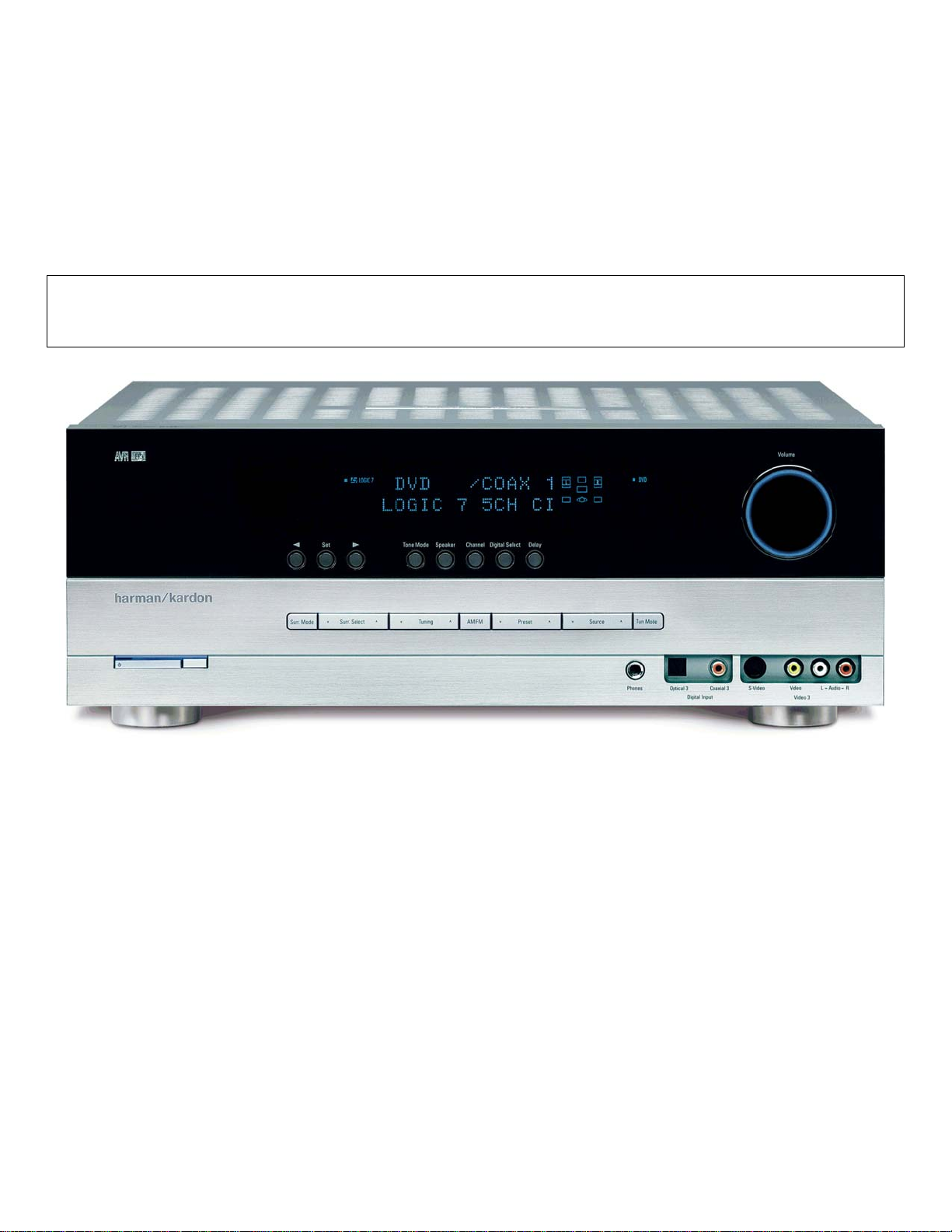
AVR145
5 X 40W 5.1 CHANNEL A/V RECEIVER
SERVICE MANUAL
CONTENTS
ESD WARNING........................ 2 ELECTRICAL PARTS LIST.... 12
LEAKAGE TESTING.................. 3 SEMICONDUCTOR PINOUTS 48
BASIC SPECIFICATIONS.......... 4 PCB DRAWINGS.................. 119
TROUBLESHOOTING GUIDE..... 5 BLOCK DIAGRAM................. 126
PROCESSOR RESET............... 5 WIRING DIAGRAM................ 127
PACKAGE LIST AND PARTS....... 6 AMP BIAS ADJUSTMENT 128
DISASSEMBLY 7 SCHEMATIC DIAGRAMS....... 129
UNIT EXPLODED VIEW AND PARTS 11
Released 2007
Discontinued XXXX Rev 0, 10/2007
harman/kardon, Inc.
250 Crossways Park Dr.
Woodbury, New York, 11797
Page 2
harman/kardon
AVR 145/230 service manual
Page 2 of 135
2
ELECTROSTATICALLY SENSITIVE DEVICES
AVR145
harman/kardon
Some semiconductor (solid state) devices can be damaged easily by static electricity. Such components commonly are called
Electrostatically Sensitive (ES) Devices. Examples of typical ES devices are integrated circuits and some field effect transistors and
semiconductor "chip" components.
The following techniques should be used to help reduce the incidence of component damage caused by static electricity.
1. Immediately before handling any semiconductor component or semiconductor-equipped assembly, drain off any electrostatic charge on
your body by touching a known earth ground. Alternatively, obtain and wear a commercially available discharging wrist strap device,
which should be removed for potential shock reasons prior to applying power to the unit under test.
2. After removing an electrical assembly equipped with ES devices, place the assembly on a conductive surface such as aluminum foil, to
prevent electrostatic charge build-up or exposure of the assembly.
3. Use only a grounded-tip soldering iron to solder or unsolder ES devices.
4. Use only an anti-static solder removal device. Some solder removal devices not classified as "anti-static" can generate electrical charges
sufficient to damage ES devices.
5. Do not use freon-propelled chemicals. These can generate electrical change sufficient to damage ES devices.
6. Do not remove a replacement ES device from its protective package until immediately before you are ready to install it. (Most replacement
ES devices are packaged with leads electrically shorted together by conductive foam, aluminum foil or comparable conductive material.)
7. Immediately before removing the protective material from the leads of a replacement ES device, touch the protective material to the
chassis or circuit assembly into which the device will be installed.
CAUTION :
8. Minimize bodily motions when handling unpackaged replacement ES devices. (Otherwise harmless motion such as the brushing together
or your clothes fabric or the lifting of your foot from a carpeted floor can generate static electricity sufficient to damage an ES devices.
Be sure no power is applied to the chassis or circuit, and observe all other safety precautions.
Each precaution in this manual should be followed during servicing.
Components identified with the IEC symbol in the parts list are special significance to safety. When replacing a component identified with
, use only the replacement parts designated, or parts with the same ratings or resistance, wattage, or voltage that are designated in the
parts list in this manual. Leakage-current or resistance measurements must be made to determine that exposed parts are acceptably
insulated from the supply circuit before retuming the product to the customer.
Page 3
SAFETY PRECAUTIONS
The following check should be performed for the continued
protection of the customer and service technician.
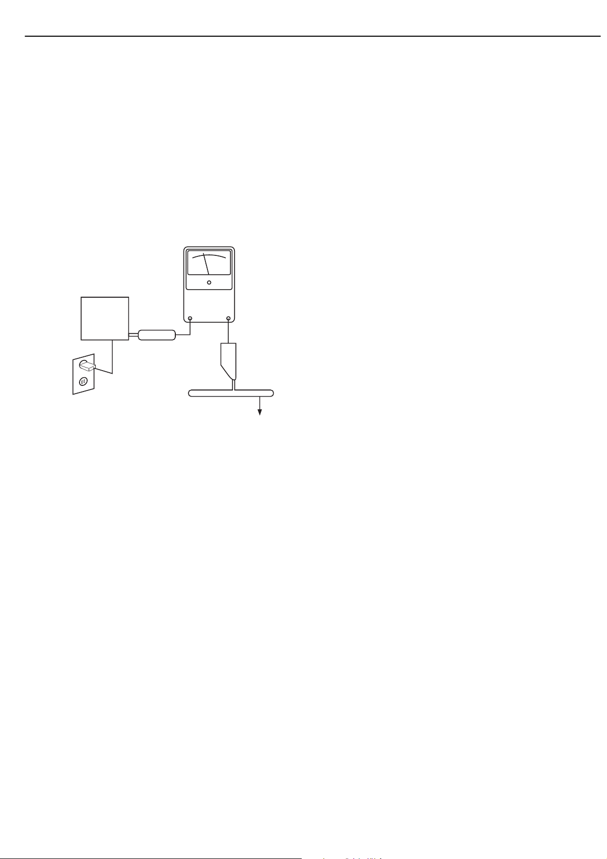
LEAKAGE CURRENT CHECK
Measure leakage current to a known earth ground (water
pipe, conduit, etc.) by connecting a leakage current tester
between the earth ground and all exposed metal parts of the
appliance (input/output terminals, screwheads, metal
overlays, control shaft, etc.). Plug the AC line cord of the
appliance directly into a 120V AC 60Hz outlet and turn the
AC power switch on. Any current measured must not exceed
o.5mA.
ANY MEASUREMENTS NOT WITHIN THE LIMITS
OUTLINED ABOVE ARE INDICATIVE OF A
POTENTIAL SHOCK HAZARD AND MUST BE
CORRECTED BEFORE RETURNING THE APPLIANCE
TO THE CUSTOMER.
harman/kardon
AVR 145/230 service manual
Page 3 of 135
Reading should
not be above
0.5mA
Earth
ground
Device
under
test
Test all
exposed metal
surfaces
Also test with
plug reversed
(Using AC adapter
plug as required)
Leakage
current
tester
AC Leakage Test
Page 4

Technical Specifications AVR145/230
harman/kardon
AVR 145/230 service manual
Page 4 of 135
Audio Section
Stereo Mode
Continuous Average Power (FTC)
50 Watts per channel, 20Hz–20kHz,
@ < 0.07% THD, both channels driven into 8 ohms
5 Channel Surround Modes
Power Per Individual Channel
Front L&R channels:
40 Watts per channel,
@ < 0.07% THD, 20Hz–20kHz into 8 ohms
Center channel:
40 Watts, @ < 0.07% THD, 20Hz–20kHz into 8 ohms
Surround channels:
40 Watts per channel,
@ < 0.07% THD, 20Hz–20kHz into 8 ohms
Input Sensitivity/Impedance
Linear (High Level) 200mV/47kohms
Signal-to-Noise Ratio (IHF-A) 100dB
Surround System Adjacent Channel Separation
Analog Decoding 40dB
(Pro Logic, etc.)
Dolby Digital (AC-3) 55dB
DTS 55dB
FM Tuner Section
Frequency Range 87.5–108MHz
Usable Sensitivity IHF 1.3 µV/13.2dBf
Signal-to-Noise Ratio Mono/Stereo: 70/68dB (DIN)
Distortion Mono/Stereo: 0.2/0.3%
Stereo Separation 40dB @ 1kHz
Selectivity ±400kHz: 70dB
Image Rejection 80dB
IF Rejection 90dB
AM Tuner Section
Frequency Range 522–1620kHz
Signal-to-Noise Ratio 45dB
Usable Sensitivity Loop: 500µV
Distortion 1kHz, 50% Mod: 0.8%
Selectivity ±10kHz: 30dB
Video Section
Video Format PAL/NTSC
Input Level/Impedance 1Vp-p/75 ohms
Output Level/Impedance 1Vp-p/75 ohms
Video Frequency Response
(Composite and S-Video) 10Hz–8MHz (-3dB)
Video Frequency
Response (Component) 10Hz–100MHz (-3dB)
Frequency Response
@ 1W (+0dB, –3dB) 10Hz–130kHz
High Instantaneous
Current Capability (HCC) ±25 Amps
Transient Intermodulation
Distortion (TIM) Unmeasurable
Rise Time 16 µsec
Slew Rate 40V/µsec**
General
Power Requirement AC 220–240V/50Hz
Power Consumption 65W idle, 540W maximum
(5 channels driven)
Dimensions (Max)
Width 440mm
Height 165mm
Depth 382mm
Weight 9.7 kg
Depth measurement includes knobs, buttons and terminal connections.
Height measurement includes feet and chassis.
All features and specifications are subject to change without notice.
Harman Kardon, The Bridge and Logic 7 are
registered trademarks of Harman International Industries, Incorporated.
*Manufactured under license from Dolby Laboratories.
“Dolby,”“Pro Logic” and the Double-D symbol are trademarks of Dolby Laboratories.
"DTS" and "DTS Neo:6" are registered trademarks of DTS,
Inc. "96/24" is a trademark of DTS,Inc.
SA-CD is a trademark of Sony Electronics, Inc.
Apple and iPod are registered trademarks of Apple Computer,Inc.
Cirrus is a registered trademark of Cirrus Logic Corp.
**Without input anti slewing and output isolation networks.
TM
is a trademark of Harman International Industries, Inc.
Page 5

45
TROUBLESHOOTING GUIDE
SYMPTOM CAUSE SOLUTION
Unit does not function when Main • No AC Power • Make certain AC power cord is plugged into
Power Switch is pushed a live outlet
• Check to see whether outlet is switch-controlled
Display lights,but no sound • Intermittent input connections • Make certain that all input and speaker connections
or picture are secure
• Mute is on • Press Mute Button
• Volume control is down • Turn up volume control
No sound from any speaker; • Amplifier is in protection mode • Check speaker wire connections for shorts at receiver and
light around power switch is red due to possible short speaker ends
• Amplifier is in protection mode • Contact your local Harman Kardon service center
due to internal problems
No sound from surround or • Incorrect surround mode • Select a mode other than Stereo
center speakers • Input is monaural • There is no surround information from mono sources
• Incorrect configuration • Check speaker mode configuration
• Stereo or Mono program material • The surround decoder may not create center- or rear-channel
information from nonencoded programs
Unit does not respond to • Weak batteries in remote • Change remote batteries
remote commands • Wrong device selected • Press the AVR selector
• Remote sensor is obscured • Make certain front panel sensor is visible to remote
or connect an optional remote sensor
Intermittent buzzing in tuner • Local interference • Move unit or antenna away from computers,fluorescent
lights,motors or other electrical appliances
Letters flash in the channel indicator • Digital audio feed paused • Resume play for DVD
display and digital audio stops • Check that Digital Input is selected
In addition to the items shown above,additional information on troubleshooting possible problems with your AVR 145,or installation-related issues, may
be found in the list of "Frequently Asked Questions" which is located in the Product Support section of our Web site at www.harmankardon.com.
harman/kardon
AVR 145/230 service manual
Page 5 of 135
Page 6
1. Instruction manual ass'y - Accessories
harman/kardon
AVR 145/230 service manual
Page 6 of 135
2. Package Drawing
AVR145/230
1
5
9
POLY BAG
COVER ASS'Y
POLY BAG
2
AM LOOP ANTENNA ASS'Y
6
IMAGE BROCHURES
10
BOOKLET,INFORMATION
3
BATTERY ASS'Y
7
REMOCON
TRANSMITTER ASS'Y
11
MANUAL INSTRUCTION
4
FM 1 POLE ANT
8
STAPLE
12
MANUAL SETUP CODE
2
SNOW PAD (L)
SET
4
ACCESSORY-1
1
SNOW PAD (R)
3
BOX ,OUT CARTON
5
ACCESSORY-1
NO
1
2
3
4
5
6
7
8 STAPLE CPL0905 3
DESCRIPTION
POLY BAG
AM LOOP ANTENNA ASS'Y
BATTERY 3
FM 1 POL ANT
COVER ASS'Y
1
COVER A
2
COVER B
SHEET,FRONT COVER
3
PAD , COVER
4
5
BAG , POLY
IMAGE BROCHURES
REMOCON ASS'Y CARTAVR145/230 1
PARTS NO. Q,ty
CPB1061Y
CSA1A027Z
CABR03P3
CSA1A018Z 1
CGRAVR130/230ZA
CGR1A331M7H43 1
CQE1A220Z
CPS1A676 1
CPB1A176Z 1
HQE1A273Z
13
1
1
STAPLE
1
1
NO
1CGR1A332M7H43
1
1
9
BOOKLET,INFORMATION
10
11
12
MANUAL ,SETUP GUIDE
13
STAPLE CPL0905 3
ACCESSORY-2
DESCRIPTION
PARTS NO. Q,ty
CQE1A180Z 1
CQX1A1135YMANUAL,INSTRUCTION
CQX1A1138X
DESCRIPTIONNO
ACCESSORY-1
1CPB1061YPOLY BAG
1
1
1
SNOW,PAD(L)
2
3
SNOW,PAD(R)
4
SET
BOX,OUT CARTON5
6
ACCESSORY-2 CQXAVR145/230
CQXAVR145/230
CPS4A564
CPS4A565
AVR145/230SET
CPG1A820W
Q,tyPARTS NO.
1
1
1
1
6
1
1
ACCESSORY-2
Page 7
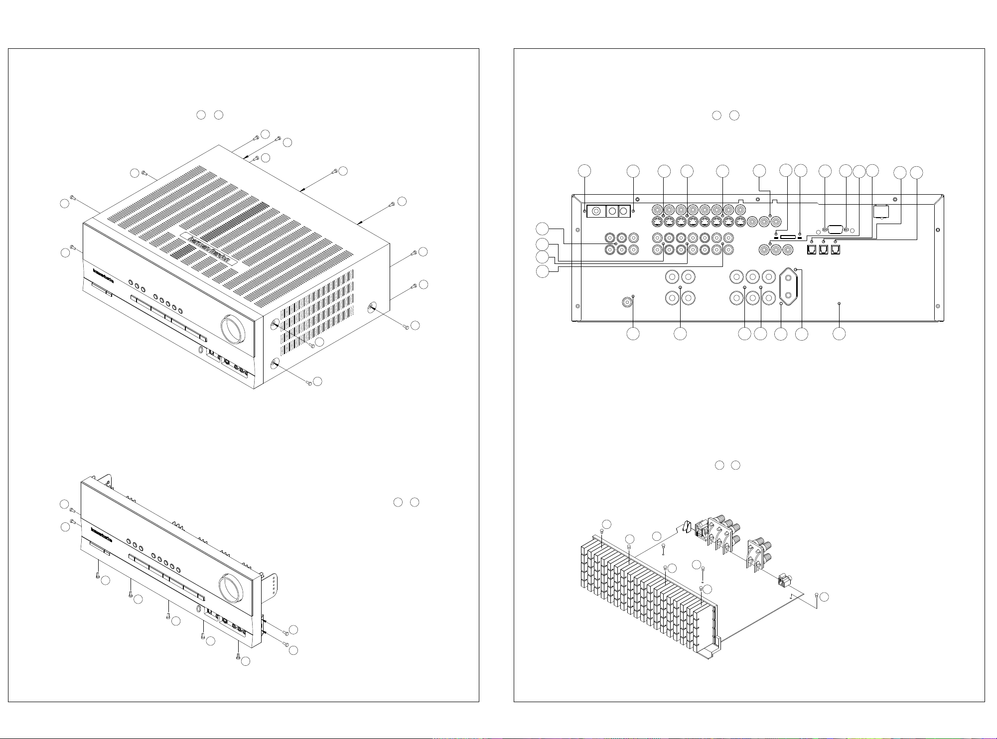
DISASSEMBLY
harman/kardon
AVR 145/230 service manual
Page 7 of 135
AVR145/230
1. Removing the Top Cabinet
Remove the Screws
6
4
5
3. Removing the Rear Panel
13
1
~
10
9
11
7
8
12
13
3
1
2
Remove the Screws
6
7
8
9
10
19
5
4 3 2
20 21 22
25
1
~
11
23
12
24
13
25
1
14
15
16
17 18
9
8
7
4. Removing the Main PCB
1 7
Remove the Screws
~
2. Removing the Front Panel
Remove the Screws
6
5
1
4
2
3
1 9
~
1
5
2
6
3
4
7
Page 8

Page 8 of 135
AVR145
harman/kardon
AVR145 DISASSEMBLY PROCEDURE
1 TOP-CABINET (21) REMOVAL
1. Remove 13 screws (S1,S7) and then remove the Top-cabinet.
2 FRONT PANEL ASS’Y REMOVAL
1. Remove the Top-cabinet, referring to the previous step 1.
2. Disconnect the card cable between connector (CN72-17p) on the FIP PCB (37-1) and connector (CN72) on the Input PCB (39-1).
3. Disconnect the lead wire (BN81-8P) on the FIP PCB (37-1) from connector (CN81) on the Trans PCB (40-4).
4. Disconnect the lead wire (BN22-6P) on the Phone PCB (37-5) from connector (CN22) on the Input PCB (39-1).
5. Disconnect the lead wire (BN18-5P) on the Phone PCB (37-5) from connector (CN18) on the Input PCB (39-1)
6. Disconnect the lead wire (BN10-4P) on the Volume PCB (37-6) from connector (CN10) on the Input PCB (39-1)
7. Disconnect the lead wire (BN41-6P) on the Volume PCB (37-6) from connector (CN41) on the Video PCB (41)
8. Remove 1 screw (S10) and then lead wire (JW82-1P,JW83-1P) on the Phone PCB (37-5).
9 .Remove 1screw (S10) and then lead wire (JW84-1P) on the Volume PCB (37-3).
10. Remove 10 screws (S1) and then remove the Front Panel ASS’Y.
3 VOLUME PCB (37-6) REMOVAL
1. Remo ve the Top-cabinet, r eferring to t he prev iou s step 1.
2. Remove the Front Panel ASS’Y, referring to the previous step 2.
3. Pull out the Volume Knob ASS’Y.
4. Disconnect connector (CN84) on the Volume PCB (37-6) from the lead wire (BN84-5P) on the FIP PCB (37-1).
5. Remove 8 screws (S2,S14), and then remove the Volume PCB (37-6).
4 PHONE PCB (37-5) REMOVAL
1. Remo ve the Top-cabinet, r eferring to t he prev iou s step 1.
2. Remove the Front Panel ASS’Y, referring to the previous step 2.
3.. Disconnect connector (CN85)on the Phone PCB (37-5) from the lead wire (BN85-2P) on the FIP PCB (37-1).
4. Remove 2 screws (S2) and then remove the Phone PCB (37-5).
5 POWER LED PCB (37-3) REMOVAL
1. Remo ve the Top-cabinet, r eferring to t he prev iou s step 1.
2. Remove the Front Panel ASS’Y, referring to the previous step 2.
3. Disconnect connector (CN88) on the Power Led PCB (37-3) from the lead wire (BN88-4P) on the FIP PCB (37-1) .
4. Remove 2 screws (S2) and then remove the Power led PCB (37-3).
6 FIP PCB (37-1) REMOVAL
1. Remo ve the Top-cabinet, r eferring to t he prev iou s step 1.
2. Remove the Front Panel ASS’Y, referring to the previous step 2.
3. Disconnect the lead wire (BN84-5P) on the FIP PCB (37-1) from connector (CN84) on the Volume PCB (37-6).
4. Disconnect the lead wire (BN85-2P) on the FIP PCB (37-1) from connector (CN85) on the Phone PCB (37-5).
5. Disconnect the lead wire (BN88-4P) on the FIP PCB (37-1) from connector (CN88) on the Power Led PCB (37-3).
6. Disconnect the connector (CN89) on the FIP PCB (37-1) from lead wire (BN89-4P) on the Key PCB (37-2).
7. Remove 3 screws (S2) and then remove the Guide PCB (37-8) & the FIP PCB (37-1).
7 KEY PCB (37-2) REMOVAL
1. Remo ve the Top-cabinet, r eferring to t he prev iou s step 1.
2. Remove the Front Panel ASS’Y, referring to the previous step 2.
3. Remove the FIP PCB (37-1), referring to the previous step6.
4. Remove 10 screws (S2) and then remove the Key PCB (37-2).
Page 9

Page 9 of 135
AVR145
harman/kardon
8 TUNER MODULE (42) REMOVAL
1. Remove the Top-cabinet, referring to the previous step 1.
2. Disconnect the card cable between connector (CON1-13p) on the Tuner module (42) and connector (CN13) on Input PCB (39-1).
3. Remove 2 screws (S8) and then remove the Tuner Module (42).
9 VIDEO PCB (41) REMOVAL
1. Remove the Top-cabinet, referring to the previous step 1.
2. Disconnect the card cable between connector (BN14-13p) on the Video PCB (41) and connector (CN14) on the Input PCB (39-1).
3. Disconnect connector (CN43 ) on the Vide o PCB (41 ) from the lead wire (BN43-4P ) on the Re gulator PCB (A)(40 -2) .
4. Disconnect the card cable between connector (CN42) on the Video PCB (41) and connector (BN44-7p) on the I-Pod PCB (39-2).
5. Disconnect connector (CN41) on the Video PCB (41) from the lead wire (BN41-6P) on the Volume PCB (37-6).
6. Remove 6 screws (S8) and then remove the Video PCB (41).
10 I-POD PCB (39-2) REMOVAL
1. Remove the Top-cabinet, referring to the previous step 1.
2. Remove the Video PCB (41), referring to the previous step9
3. Disconnect connector (CN46) on the I-Pod PCB (39-2) from the lead wire (BN46-3P) on the Input PCB (39-1).
4. Disconnect the card cable between connector (BN19-9p)) on the I-Pod PCB (39-2) and connector (CN19) on the Input PCB (39-1).
5. Disconnect the card cable between connector (BN44-7p)) on the I-Pod PCB (39-2) and connector (CN42) on the Video PCB (41).
6. Disconnect the card cable between connector (CN47-7p)) on the I-Pod PCB (39-2) and connector (CN47) on the RS232 PCB (37-7).
7. Remove 2 screws (S13) and then remove the I-Pod PCB (39-2).
11 RS232 PCB (37-7) REMOVAL
1. Remove the Top-cabinet, referring to the previous step 1.
2. Remove the Video PCB (41), referring to the previous step9
3. Disconnect the card cable between connector (CN47) on the RS232 PCB (37-7) and connector (CN47-7) on the RS232 PCB (37-7).
4. Remove 2 screws and then remove the RS232 PCB (37-7).
12 INPUT PCB (39-1) REMOVAL
1. Remove the Top-cabinet, referring to the previous step 1.
2. Remove the Tuner module (42), referring to the previous step8
3. Remove the Video PCB (41), referring to the previous step9
4. Disconnect connector (CN20) on the the Input PCB (39-1) from the lead wire (BN20-5P) on the Regulator PCB (B)(40-5).
5. Disconnect connector (CN22) on the Input PCB (39-1) from the lead wire (BN22-6P) on the Phone PCB (37-5).
6. Disconnect connector (CN18) on the Input PCB (39-1) from the lead wire (BN18-5P) on the Phone PCB (37-5)
7. Disconnect connector (CN10) on the Input PCB (39-1) from the lead wire (BN10-4P) on the Volume PCB (37-6).
8. Disconnect the card cable between connector (CN14) on the Input PCB (39-1) and connector (BN14-13p)) on the Video PCB (41).
9. Disconnect the card cable between connector (CN19) on the Input PCB (39-1) and connector (BN19-9p) on the I-Pod PCB (39-2)
10. Disconnect the lead wire (BN46-3P) on the Input PCB (39-1) from connector (CN46) on the I-Pod PCB (39-2).
11. Disconnect the card cable between connector (CN12-21p) on the Input PCB (39-1) and connector (CN12-21p)
on the main PCB (38-1)
12. Disconnect the card cable between connector (CN11-13p) on the Input PCB (39-1) and connector (CN11) on the main PCB (38-1)
13. Disconnect the card cable between connector (CN72) on the Input PCB (39-1) and connector (CN72-17p) on the FIP PCB (37-1)
14. Remove 11 screws (S8,S15) and then remove the Input PCB (39-1).
13 POWER TRANS (36) & POWER PCB ASS’Y(40) REMOVAL
1. Remove the Top-cabinet, referring to the previous step 1.
2. Disconnect lead wire of the Power Trans (36) from connector (CN91-3P) on the Main PCB (38-1)
3. Disconnect connector (CN19-3P,CN20-4P) on TRANS PCB (40-3) from the lead wire (BN19-3P,BN20-4P) on the Main PCB (38-1).
4. Disconnect the lead wire (BN96-8P) on the Power PCB (40-4) from connector (CN96) on the Regulator PCB (B)(40-5).
5. Disconnect the lead wire (BN99-8P) on the Power PCB (40-4) from connector (CN99) on the Regulator PCB (A)(40-2).
6. Disconnect connector (CN81) on the Trans PCB (40-4) from the lead wire (BN81-8P) on the FIP PCB (37-1).
7. Remove 4 Trans screws (S9) and then remove the Power Trans (36)& Power PCB ASS’Y(40) REMOVAL .
Page 10

Page 10 of 135
AVR145
harman/kardon
14 MAIN PCB AS S ’Y (38 -1 ) REMOVA L
1. Remove the Top-cabinet, referring to the previous step 1.
2. Remove the Tuner module (42), referring to the previous step8.
3. Remove the Video PCB (41) referring to the previous step9.
4. Remove the I-Pod PCB (39-2), referring to the previous step 10.
5. Remove the RS232 PCB (37-7), referring to the previous step 11.
6. Remove the Input PCB (39-1), referring to the previous step 12.
7. Remove the AC Cord(35) on the Main PCB (38-1)
8. Disconnect the lead wire (BN90-2P) on the Main PCB (38-1) from connector (CN86) on Moms PCB (37-4).
9. Disconnect connector (CN91-3P) on the Main PCB (38-1) from lead wire of the Power Trans (36)
10. Disconnect the lead wire (BN89-2P) on the Main PCB (38-1) from connector (CN89) on Regulator PCB (A)(40-2).
11. Disconnect the lead wire (BN19-3P,BN20-4P) on the Main PCB (38-1) from connector (CN19-3P,CN20-4P) on TRANS PCB (40-4).
12. Remove 11screws (S13-1EA, S4-2EA, S6-2EA, S8-6EA) and then remove the Main PCB ASS’Y (38-1).
Page 11
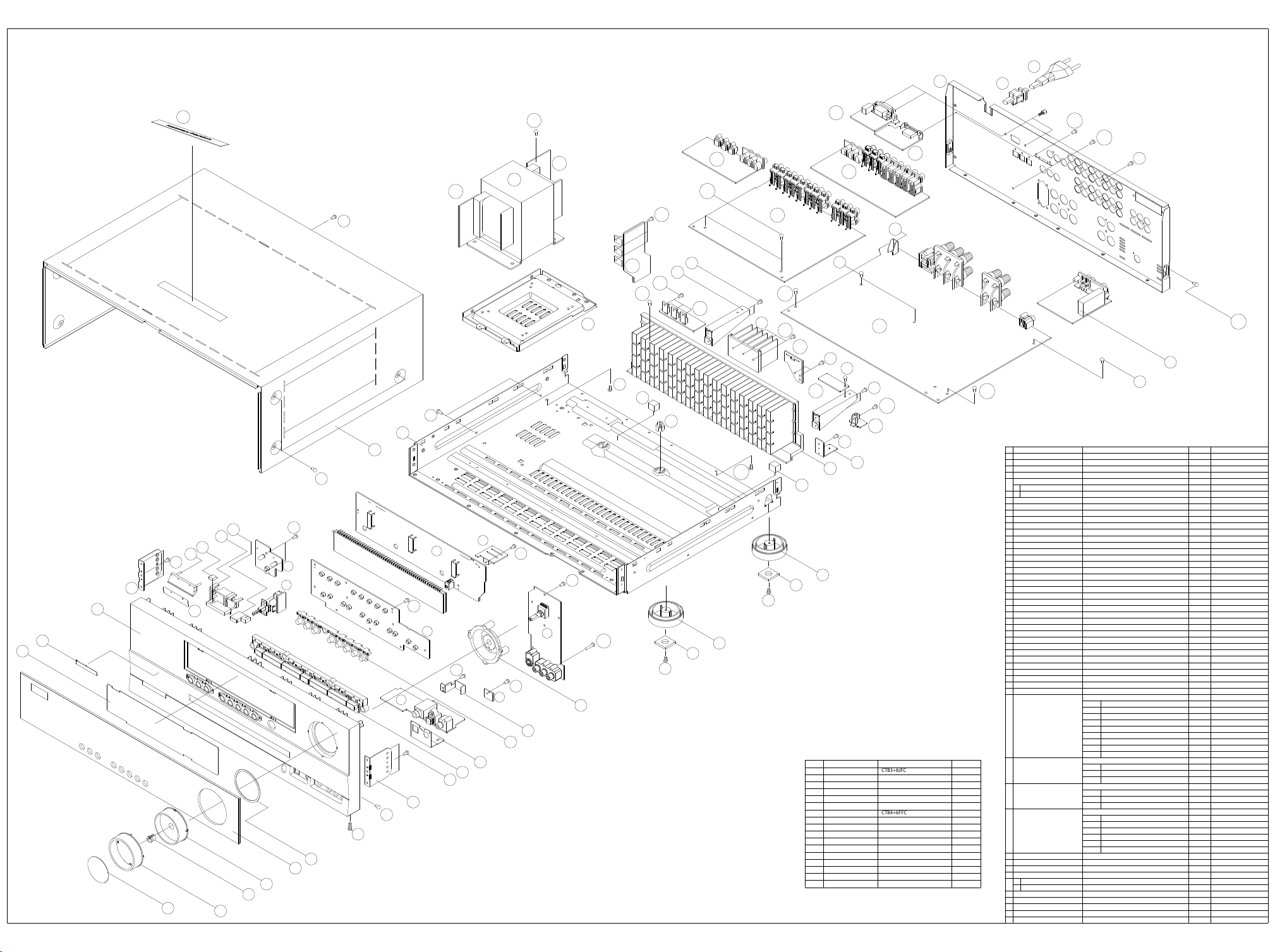
AVR145/230 EXPLODED VIEW
harman/kardon
AVR 145/230 service manual
Page 11 of 135
Only screws marked in yellow are stocked
33
35
34
44
S9
37-7
S13
S13
40-3
36
40-4
40-5
S16
30
S1
40-1
41
S15
39-1
S6
S5
x2
39-2
32
S8
S16
S17
S4
40-2
29
45
S12
38-1
S10
38-2
S4
S4
S5
43
S5
28
39-3
22
21
S7
37-4
37-3
S2
37-1
37-8
S2
S2
S2
37-2
37-6
S11
23
S2
S4
15
13
14-1
14
S2
10
9
18
8
7
S10
S4
24
26
25
24
23
S2
37-5
37-9
19
16
12
17
11
S2
10
S1
S1
6
5
4
DESCRIPTION PARTS NO. Q,ty
NO
S1
SCREW
S2
SCREW
S3
SCREW
S4
SCREW
S5
SCREW
S6
SCREW
S7
SCREW
S8
SCREW,TRANS
S9
SCREW
S10
SCREW
S11
SCREW CTB3+10JR 3
S12
SCREW
S13
SCREW,SPECIAL CHD1A012R 18
S14
SCREW,SPECIAL
S15
SCREW,SPECIAL
S16
SCREW,SPECIAL
S17
3
1
2
S5
S15
S14
40-2
S5
27
CTB3+10GR
CTWS3+10GR
CTW3+8JR
CTB3+8JR
CTW3+12JR
CTB4+6FFC
CTB3+10GFZR
CHD1A023R
CTB3+6JR
CTB3+16GFZR
CTB3+8JFZR
CHD1A012ZR 2
CHD3A012R 6
CHD4A012R 5
17CTB3+8JFCSCREW
35
1
9
10
3
6
19
4
19
2
3
DESCRIPTION
NO
ORNAMENT,VOLUME CGU1A318Z 1
1
CAP,VOLUME
2
HOLDER,VOLUME
3
INDICATOR,VOLUME
4
WINDOW ASS'Y
5
WINDOW,FIP CGU1A399Y
1
BADGE,MODEL
2
6
FILTER,FIP
7
BDAGE,HARMAN/KARDON
8
PANEL,FRONT
9
BRACKET,SIDE
10
KNOB,FUNCTION
11
KNOB,DISPLAY
12
KNOB,POWER
13
INDICATOR,POWER
14
KNOB,MOMS
15
BRACKET,PCB CMK2A010
16
PLATE,SHIELD
17
SHEET , REFLECTION CMZ1A120 1
18
HOLDER,LED
19
BRACKET,FIP
20
CABINET,TOP
21
CHASSIS,BOTTOM
22
RUBBER,CUSHION
23
FOOT
24
SUPPORT,CUSHION
25
HEAT SINK
26
BRACKET,PCB
27
HOLDER,PCB
28
BRACKET,TRANS
29
BRACKET,PCB(H/T)
30
BRACKET,PCB CMD1A570 1
31
BRACKET,PCB
32
PANEL,REAR
33
BUSHING,AC CORD
34
CORD,POWER
35
TRANS,POWER
36
FRONT PCB ASS'Y
37
MAIN PCB ASS'Y COP11911E 1
38
INPUT PCB ASS'Y COP11912E 1
39
POWER PCB ASS'Y
40
VIDEO PCB ASS'Y
41
TUNER MODULE
42
43
BADGE ASS'Y
44
ORNAMENT,BADGE
1
BADGE,H/K(TOP)
2
45
PARTS NO.
CGX1A338MBC63
CMH1A214
CGL1A222
CGUAVR145
CGB1A168Z
CMZ2A090SHEET,VOLUME 1
CMZ1A088
KGB1A158Z
CGW1A427RDZH43
CMD2A443
CBT1A1028MBYG27
CBT1A1027K128
CBT1A1026MMZG27
CGL1A258Z
CBC1A158MBZG27
CMC1A302
CMH1A215
CMD1A209
CKC5B145S46Z
CUA2A229
CHG1A329
CKL2A069H43
CHG1A104Z
CMY2A269
CMD1A417
CHE1A170
CMD1A487
CMD1A398
CMD1A387
CKF4A319Z
KHR1A028
CJA2B043ZA
CLT5V045ZE
COP11910E
FIP PCB
37-1
KEY PCB
37-2
POWER LED PCB
37-3
MOMS PCB
37-4
PHONE PCB
37-5
VOLUME PCB
37-6
RS232 PCB
37-7
GUIDE PCB(CARD CABLE)
37-8
MAIN PCB
38-1
GUIDE PCB(CARD CABLE) 1
38-2
INPUT PCB
39-1
iPOD PCB 1
39-2
RDS PCB 1
39-3
COP11916E 1
DIGITAL IN OUT PCB 1
40-1
REGULATOR PCB(A) 5
40-2
TRANS PCB 1
40-3
TRANS PCB 1
40-4
REGELATOR PCB(B) 1
40-5
COP11917E 1
CNVM9014MS171L
CHG1A160ZCUSHION 1
CGX1A375ZA
CGX1A375M7G32
KGB1A159Z
CMY1A249HEAT SINK 1
42
S4
Q,ty
Weright
1
1
1
1
1
1
1
1
1
2
11
1
1
1
1
1
1
3
1
1
4
4
1
1
2
2
1
2
2
1
1
1
1
1
1
1
1
1
1
1
1
1
1
1
1
1
1
1
1
Page 12

AVR145/230 Electrical Parts List
harman/kardon
AVR 145/230 service manual
Page 12 of 135
Ref. # Part Number
CGL1A222 INDICATOR , VOLUME INDICATOR 1
CGUAVR145 WINDOW ASS'Y ASS'Y 1
CGB1A168Z BADGE , AVR145 BADGE 1
CGU1A399Y WINDOW , FIP FIP WINDOW 1
CGU1A318Z ORNAMENT , VOLUME ORNAMENT 1
CGX1A338MBC63 CAP , VOLUME CAP 1
CGX1A375ZA BADGE ASS'Y ASS'Y 1
CGX1A375M7G32 ORNAMENT , BADGE ORNAMENT 1
KGB1A159Z BADGE , HARMAN/KARDON(TOP) BADGE 1
CKC5B145S46Z CABINET , TOP TOP CABINET 1
BKC5C145S46 TOP CABINET TOP CABINET 1
CMH1A214 HOLDER , VOLUME HOLDER 1
CMZ2A090 SHEET,VOLUME SHEET 1
CQB1A549Z LABEL , ATTENTION LABEL 1
CQB1A551Z LABEL , BAR CODE LABEL 1
CQB1A622 LABEL , SERIAL NO LABEL 1
CTB3+8JFC SCREW SCREW 13
CTB4+6FFC SCREW SCREW 6
CHE154 CLAMPER , ARM CLAMPER 0,12
CPG1A820W BOX , OUT CARTON BOX 1
CPS4A564 PAD , SNOW L PAD 1
CPS4A565 PAD , SNOW R PAD 1
CQB1A551Z LABEL , BAR CODE LABEL 2
CQB1A795Z LABEL , COUNTRY(AVR245/230) LABEL 2
CQS1A001 RIBON , BAR CODE SONY(TR-4070) 0,12
CQXAVR145/230 INSTRUCTION MANUAL ASS'Y ASS'Y 1
CARTAVR145/230 REMOCON ASS'Y ASS'Y 1
CGRAVR130/230ZA COVER ASS'Y ASS'Y 1
CGR1A331M7H43 COVER A COVER 1
CGR1A332M7H43 COVER B COVER 1
CPS1A676 PAD , COVER PAD 1
CQE1A220Z SHEET , FRONT COVER SHEET 1
CPL0905 STAPLE STAPLE 6
CQE1A180Z BOOKLET , IMFORMATIONS BOOKLET 1
CQX1A1135Y MANUAL , INSTRUCTION AVR145/23 MANUAL 1
CQX1A1138X MANUAL , SETUP(AVR145/230) MANUAL 1
CSA1A018Z FM 1 POLE ANT ANT 1
HQE1A273Z HARMAN IMAGE BROCHURES BROCHURES 1
CRE1A037 LOCKER LOCKER 10
KPL6500 STAPLE STAPLE 8
Description
Value Qty
BOTTOM CHASSIS ASS'Y
Ref. # Part Number
CUAAVR145/230 BOTTOM CHASSIS ASS'Y ASS'Y 1
CHD1A012ZR SCREW , SPECIAL Not stocked 2
CHD1A023R SCREW , SPECIAL Not stocked 4
CHD4A012R SCREW , SPECIAL Not stocked 5
CHE170 HOLDER , PCB HOLDER 2
Description
Value Qty
Page 13

BOTTOM CHASSIS ASS'Y
Y
harman/kardon
AVR 145/230 service manual
Page 13 of 135
Ref. # Part Number
CHE36-3 CLAMPER , WIRE CLAMPER 1
CHG1A104Z CUSHION , RUBBER CUSHION 1
CHG1A160Z CUSHION , RUBBER CUSHION 1
CHG1A360 CUSHION , FOOT CUSHION 4
CHS1A032 HEMELON TAPE TAPE 5
CJA2B043ZA CORD , POWER(EUR) QDR-7100CC 1
CKF4A319Z PANEL , REAR PANEL 1
CKL2A069H43 FOOT FOOT 4
CLZ9W003Z FERRITE , RING FERRITE RING 1
CMD1A487 BRACKET , TRANS BARCKET 1
CNVM9014MS171L MODULE , TUNER(EUR) TUNER 1
CQB1A173Y LABEL, FUSE CAUTION LABEL 1
CTB3+10GFZR SCREW Not stocked 20
CTB3+6FFZR SCREW Not stocked 3
CTB3+6JR SCREW Not stocked 13
CTB3+8JR SCREW Not stocked 7
CTW3+12JR SCREW Not stocked 2
CTW3+8JR SCREW Not stocked 8
CUA2A229 CHASSIS , BOTTOM CHASSIS 1
KHR1A028 BUSHING , AC CORD AC CORD 1
CB11 CWC1B2A13A100B CABLE , CARD CARD CABLE 1
CB12 CWC1C4A21B110B CABLE , CARD CARD CABLE 1
CB13 CWC1C4A13B080B CABLE , CARD CARD CABLE 1
CB14 CWC1B2A13A100B CABLE , CARD CARD CABLE 1
CB19 CWC1B2A09A240B CABLE , CARD CARD CABLE 1
CB42 CWC1B2A07A120B CABLE, CARD (1mm PITCH, A-B TY CARD CABLE 1
CB47 CWC1B2A07A060B CABLE , CARD CARD CABLE 1
F901 KBA2C4000TLEZ FUSE(233TPYE,4A,250V) LITTLE FUSE 1
T901 CLT5V045ZE TRANS , POWER MAIN MAIN TRANS 1
Description
Value Qty
FRONT PANEL ASS
Ref. # Part Number
CGWAVR145/230 FRONT PANEL ASS'Y ASS'Y 1
CBC1A158MBZG27 KNOB , MOMS KNOB 1
CBT1A1026MMZG27 KNOB , POWER KNOB 1
CBT1A1027K128 KNOB , DISPLAY KNOB 1
CBT1A1028MBYG27 KNOB , FUNCTION KNOB 1
CGL1A258Z INDICATOR , POWER INDICATOR 1
CGW1A427RDZH43 PANEL , FRONT PANEL 1
CHR301 CLAMPER CLAMPER 12
CMC1A302 PLATE , SHIELD PLATE 1
CMD2A443 BRACKET , SIDE BRACKET 2
CMH1A215 HOLDER , LED HOLDER 1
CMK2A010 BRACKET , PCB BRACKET 1
CMZ1A088 FILTER , FIP FIP 1
CMZ1A120 SHEET , REFLECTION SHEET 1
CTB3+10GR SCREW Not stocked 31
CTB3+16GFZR SCREW Not stocked 2
KGB1A158Z BADGE , HARMAN/KARDON(FRONT) BADGE 1
CB72 CWC1B2A17A230B WAFER, CARD CABLE (1mm PITCH, WAFER 1
Description
Value Qty
Page 14

FRONT PCB ASSY
harman/kardon
AVR 145/230 service manual
Page 14 of 135
Ref. # Part Number
COP11910E FRONT PCB ASS'Y(AVR145/230) ASS'Y 1
C714 HCBS1H151KBT CAP , CERAMIC 150UF 50V K 1
C716 CCEA1AH331T CAP , ELECT 330UF 10V 1
C719 HCBS1H102KBT CAP , CERAMIC 1000PF 50V K 1
C720 HCBS1H102KBT CAP , CERAMIC 1000PF 50V K 1
C721 HCBS1H102KBT CAP , CERAMIC 1000PF 50V K 1
C723 HCBS1H104ZFT CAP , CERAMIC 0.1UF 50V Z 1
C728 HCBS1H104ZFT CAP , CERAMIC 0.1UF 50V Z 1
C729 HCBS1H473ZFT CAP , CERAMIC 0.047UF 50V Z 1
C731 CCEA1HH100T CAP , ELECT 10UF 50V 1
C735 CCEA1CKS100T CAP , ELECT 10UF 16V 1
C742 HCBS1H223ZFT CAP , CERAMIC 0.02UF 50V Z 1
C793 HCBS1H104ZFT CAP , CERAMIC 0.1UF 50V Z 1
C794 HCBS1C222MXT CAP , CERAMIC 2200PF 16V 1
C795 HCBS1H102KBT CAP , CERAMIC 1000PF 50V K 1
C796 HCBS1H102KBT CAP , CERAMIC 1000PF 50V K 1
C805 HCBS1H223ZFT CAP , CERAMIC 0.022UF 50V Z 1
C806 HCBS1H223ZFT CAP , CERAMIC 0.022UF 50V Z 1
C807 HCBS1H104ZFT CAP , CERAMIC 0.1UF 50V Z 1
C808 HCBS1H181KBT CAP , CERAMIC 180PF 50V Z 1
C809 CCEA1AH471T CAP , ELECT 470UF 10V 1
C812 HCBS1H104ZFT CAP , CERAMIC 0.1UF 50V Z 1
C817 HCBS1H100JCT CAP , CERAMIC 10PF 50V 1
C841 CCEA1HH100T CAP , ELECT 10UF 50V 1
C842 CCEA1HH100T CAP , ELECT 10UF 50V 1
C843 CCEA1HH100T CAP , ELECT 10UF 50V 1
C850 HCBS1H471KBT CAP , CERAMIC 470PF 50V 1
C851 HCBS1H471KBT CAP , CERAMIC 470PF 50V 1
C852 HCBS1H104ZFT CAP , CERAMIC 0.1UF 50V Z 1
C855 HCBS1H101KBT CAP , CERAMIC 100PF 50V K 1
C856 HCBS1H101KBT CAP , CERAMIC 100PF 50V K 1
C857 HCBS1H104ZFT CAP , CERAMIC 0.1UF 50V Z 1
C862 HCBS1H101KBT CAP , CERAMIC 100PF 50V K 1
C863 HCBS1H101KBT CAP , CERAMIC 100PF 50V K 1
C866 CCEA1HKS100T CAP , ELECT 10UF 50V SMALL 1
C867 CCEA1HKS100T CAP , ELECT 10UF 50V SMALL 1
C868 CCEA1EKS470T CAP , ELECT 47UF 25V 1
C869 CCEA1EKS470T CAP , ELECT 47UF 25V 1
C870 HCBS1H681KBT CAP , CERAMIC 680PF 50V K 1
C871 HCBS1H681KBT CAP , CERAMIC 680PF 50V K 1
C872 CCEA1CH331T CAP , ELECT 330UF 16V 1
C873 CCEA1CH331T CAP , ELECT 330UF 16V 1
C874 HCBS1H101KBT CAP , CERAMIC 100PF 50V K 1
C882 HCBS1H104ZFT CAP , CERAMIC 0.1UF 50V Z 1
C889 HCBS1H104ZFT CAP , CERAMIC 0.1UF 50V Z 1
C891 HCBS1H223ZFT CAP , CERAMIC 0.023UF 50V Z 1
C892 HCBS1H223ZFT CAP , CERAMIC 0.023UF 50V Z 1
C893 HCBS1H223ZFT CAP , CERAMIC 0.023UF 50V Z 1
C894 CCEA1CKS100T CAP , ELECT 10UF 16V 1
Description
Value Qty
Page 15

FRONT PCB ASSY
harman/kardon
AVR 145/230 service manual
Page 15 of 135
Ref. # Part Number
C896 HCBS1H223ZFT CAP , CERAMIC 0.023UF 50V Z 1
C897 CCEA1AH471T CAP , ELECT 470UF 10V 1
C901 HCBS1H390JT CAP , CERAMIC 39PF 50V Z 1
C903 CCEA1HKS2R2T CAP , ELECT 2.2UF 50V SMALL SIZE 1
C905 CCEA1HKS2R2T CAP , ELECT 2.2UF 50V SMALL SIZE 1
C953 HCBS1H104ZFT CAP , CERAMIC 0.1UF 50V Z 1
C954 HCBS1H104ZFT CAP , CERAMIC 0.1UF 50V Z 1
C957 HCBS1H104ZFT CAP , CERAMIC 0.1UF 50V Z 1
D730 CVD1SS133MT DIODE 1SS133 1
D774 CVD1SS133MT DIODE 1SS133 1
D778 HVD1N5819T DIODE , SCHOTTKY 1N5819 1
D784 CVD1SS133MT DIODE 1SS133 1
D785 CVD1SS133MT DIODE 1SS133 1
L702 HLQ02C100KT COIL , AXAIL 10uH 1
Q701 HVTKRC107MT T.R KRC107M 1
Q722 HVTKRA107MT T.R KRA107M 1
Q724 HVTKRC107MT T.R KRC107M 1
Q725 HVTKRC107MT T.R KRC107M 1
Q734 HVTKTC2874BT T.R , MUTE KTC2874B 1
Q735 HVTKTC2874BT T.R , MUTE KTC2874B 1
Q736 HVTKTC2874BT T.R , MUTE KTC2874B 1
Q737 HVTKTC2874BT T.R , MUTE KTC2874B 1
Q738 HVTKRC107MT T.R KRC107M 1
Q739 HVTKTA1271YT T.R KTA1271Y 1
R701 CRD20TJ103T RES , CARBON 10K OHM 1/5W J 1
R704 CRD20TJ100T RES , CARBON 10 OHM 1/5W J 1
R705 CRD20TJ820T RES , CARBON 82 OHM 1/5W J 1
R706 CRD20TJ820T RES , CARBON 82 OHM 1/5W J 1
R708 CRD20TJ820T RES , CARBON 82 OHM 1/5W J 1
R709 CRD20TJ470T RES , CARBON 47 OHM 1/5W J 1
R710 CRD20TJ470T RES , CARBON 47 OHM 1/5W J 1
R711 CRD20TJ470T RES , CARBON 47 OHM 1/5W J 1
R718 CRD20TJ222T RES , CARBON 2.2K OHM 1/5W J 1
R737 CRD20TJ100T RES , CARBON 10 OHM 1/5W J 1
R747 CRD20TJ103T RES , CARBON 10K OHM 1/5W J 1
R753 CRD20TF1001T RES , CARBON 1K 1/5W F 1
R754 CRD20TF1501T RES , CARBON 1.5K 1/5W F 1
R755 CRD20TF1801T RES , CARBON 1.8K 1/5W F 1
R756 CRD20TF2701T RES , CARBON 2.7K 1/5W F 1
R757 CRD20TF3301T RES , CARBON 3.3K 1/5W F 1
R758 CRD20TF5601T RES , CARBON 5.6K 1/5W F 1
R759 CRD20TF1001T RES , CARBON 1K 1/5W F 1
R760 CRD20TF1501T RES , CARBON 1.5K 1/5W F 1
R761 CRD20TF1801T RES , CARBON 1.8K 1/5W F 1
R762 CRD20TF2701T RES , CARBON 2.7K 1/5W F 1
R763 CRD20TF3301T RES , CARBON 3.3K 1/5WF 1
R764 CRD20TF5601T RES , CARBON 5.6K 1/5W F 1
R765 CRD20TF7501T RES , CARBON 7.5K 1/5W F 1
R766 CRD20TF1001T RES , CARBON 1K 1/5W F 1
R767 CRD20TF1501T RES , CARBON 1.5K 1/5W F 1
Description
Value Qty
Page 16

FRONT PCB ASSY
harman/kardon
AVR 145/230 service manual
Page 16 of 135
Ref. # Part Number
R768 CRD20TF1801T RES , CARBON 1.8K 1/5W F 1
R769 CRD20TF2701T RES , CARBON 2.7K 1/5W F 1
R781 CRD20TJ102T RES , CARBON 1K OHM 1/5W J 1
R783 CRD20TJ102T RES , CARBON 1K OHM 1/5W J 1
R784 CRD20TJ102T RES , CARBON 1K OHM 1/5W J 1
R786 CRD20TJ152T RES , CARBON 1.5K OHM 1/5W J 1
R787 CRD20TJ101T RES , CARBON 100 OHM 1/5W J 1
R791 CRD20TJ822T RES , CARBON 8.2K OHM 1/5W J 1
R805 CRD20TJ104T RES , CARBON 100K OHM 1/5W J 1
R806 CRD20TJ472T RES , CARBON 4.7K OHM 1/5W J 1
R824 CRD20TJ221T RES , CARBON 220 OHM 1/5W J 1
R825 CRD20TJ681T RES , CARBON 680 OHM 1/5W J 1
R828 CRD20TJ221T RES , CARBON 220 OHM 1/5W J 1
R829 CRD20TJ681T RES , CARBON 680 OHM 1/5W J 1
R864 CRD20TJ272T RES , CARBON 2.7K OHM 1/5W J 1
R865 CRD20TJ101T RES , CARBON 100 OHM 1/5W J 1
R866 CRD20TJ272T RES , CARBON 2.7K OHM 1/5W J 1
R869 CRD20TJ750T RES , CARBON 75 OHM 1/5W J 1
R871 CRD20TJ104T RES , CARBON 100K OHM 1/5W J 1
R872 CRD20TJ104T RES , CARBON 100K OHM 1/5W J 1
R873 CRD20TJ471T RES , CARBON 470 OHM 1/5W J 1
R874 CRD20TJ471T RES , CARBON 470 OHM 1/5W J 1
R875 CRD20TJ103T RES , CARBON 10K OHM 1/5W J 1
R876 CRD20TJ750T RES , CARBON 75 OHM 1/5W J 1
R877 CRD20TJ750T RES , CARBON 75 OHM 1/5W J 1
R878 CRD20TJ750T RES , CARBON 75 OHM 1/5W J 1
R892 CRD20TJ222T RES , CARBON 2.2K OHM 1/5W J 1
R893 CRD20TJ333T RES , CARBON 33K OHM 1/5W J 1
R895 CRD20TJ101T RES , CARBON 100 OHM 1/5W J 1
R896 CRD20TJ101T RES , CARBON 100 OHM 1/5W J 1
R897 CRD20TJ101T RES , CARBON 100 OHM 1/5W J 1
R898 CRD20TJ101T RES , CARBON 100 OHM 1/5W J 1
R899 CRD20TJ104T RES , CARBON 100K OHM 1/5W J 1
R900 CRD20TJ104T RES , CARBON 100K OHM 1/5W J 1
R901 CRD20TJ152T RES , CARBON 1.5K OHM 1/5W J 1
R902 CRD20TJ152T RES , CARBON 1.5K OHM 1/5W J 1
R903 CRD20TJ102T RES , CARBON 1K OHM 1/5W J 1
R904 CRD20TJ102T RES , CARBON 1K OHM 1/5W J 1
R905 CRD20TJ104T RES , CARBON 100K OHM 1/5W J 1
R906 CRD20TJ104T RES , CARBON 100K OHM 1/5W J 1
R907 CRD20TJ472T RES , CARBON 4.7K OHM 1/5W J 1
R908 CRD20TJ472T RES , CARBON 4.7K OHM 1/5W J 1
R909 CRD20TJ221T RES , CARBON 220 OHM 1/5W J 1
R910 CRD20TJ221T RES , CARBON 220 OHM 1/5W J 1
R911 CRD20TJ221T RES , CARBON 220 OHM 1/5W J 1
R912 CRD20TJ221T RES , CARBON 220 OHM 1/5W J 1
R913 CRD20TJ102T RES , CARBON 1K OHM 1/5W J 1
R915 CRD20TJ473T RES , CARBON 47K OHM 1/5W J 1
R918 CRD20TJ472T RES , CARBON 4.7K OHM 1/5W J 1
R919 CRD20TJ472T RES , CARBON 4.7K OHM 1/5W J 1
Description
Value Qty
Page 17

FRONT PCB ASSY
harman/kardon
AVR 145/230 service manual
Page 17 of 135
Ref. # Part Number
R956 CRD20TJ1R0T RES , CARBON 1 OHM 1/5W J 1
S701 HST1A020ZT SW , TACT 1A020 1
S702 HST1A020ZT SW , TACT 1A020 1
S703 HST1A020ZT SW , TACT 1A020 1
S704 HST1A020ZT SW , TACT 1A020 1
S705 HST1A020ZT SW , TACT 1A020 1
S706 HST1A020ZT SW , TACT 1A020 1
S707 HST1A020ZT SW , TACT 1A020 1
S708 HST1A020ZT SW , TACT 1A020 1
S709 HST1A020ZT SW , TACT 1A020 1
S710 HST1A020ZT SW , TACT 1A020 1
S711 HST1A020ZT SW , TACT 1A020 1
S712 HST1A020ZT SW , TACT 1A020 1
S713 HST1A020ZT SW , TACT 1A020 1
S714 HST1A020ZT SW , TACT 1A020 1
S715 HST1A020ZT SW , TACT 1A020 1
S716 HST1A020ZT SW , TACT 1A020 1
S717 HST1A020ZT SW , TACT 1A020 1
S718 HST1A020ZT SW , TACT 1A020 1
S719 HST1A020ZT SW , TACT 1A020 1
S720 HST1A020ZT SW , TACT 1A020 1
CMC3A111 PLATE , EARTH PLATE 1
BK71 CMD1A209 BRACKET , FLT BRACKET 1
BK72 CMD1A209 BRACKET , FLT BRACKET 1
BK73 CMD1A209 BRACKET , FLT BRACKET 1
BN10 CWZAVR230BN10 WIRE ASS'Y (SHIELD) WIRE 1
BN18 CWZAVR125BN18 WIRE ASS'Y (SHIELD) WIRE 1
BN22 CWZAVR145BN22 WIRE ASS'Y (SHIELD) WIRE 1
BN41 CWZAVR130BN41 WIRE ASS'Y (SHIELD) WIRE 1
BN81 CWB2C908200BM WIRE ASS'Y WIRE 1
BN84 CWB2B905080EN WIRE ASS'Y WIRE 1
BN85 CWB2B902100EW WIRE ASS'Y ( ANGLE ) WIRE 1
BN88 CWB2B904100EN WIRE ASS'Y WIRE 1
BN89 CWB2B904100EN WIRE ASS'Y WIRE 1
CN47 CJP07GA117ZY TEMP ITEM WAFER 1
CN72 CJP17GA193ZY WAFER, CARD CABLE (SMD) WAFER 1
CN84 CJP05GB46ZY WAFER WAFER 1
CN85 CJP02GA19ZY WAFER, 2PIN WAFER 1
CN86 CJP02GA89ZM WAFER WAFER 1
CN88 CJP04GB46ZY WAFER WAFER 1
CN89 CJP04GB46ZY WAFER WAFER 1
D701 CVD52CSBBCEAB2 BLUE L.E.D L.E.D 1
D703 CVD52CSBBCEAB2 BLUE L.E.D L.E.D 1
D705 CVD52CSBBCEAB2 BLUE L.E.D L.E.D 1
D723 CVD50BOBBWGA L.E.D , 2 COLOR (ORG , BLUE) L.E.D 1
D727 CVD50BOBBWGA L.E.D , 2 COLOR (ORG , BLUE) L.E.D 1
ET03 CMD1A569 BRACKET , PCB BRACKET 1
FIP1 HFLHCA18ML03 F.I.P FIP 1
IC73 HRVNJL34H380A SENSOR , REMOTE JRC 1
IC75 HVI74ACT04MTR I.C , HEX INVERTER FAIRCHILD 1
Description
Value Qty
Page 18

FRONT PCB ASSY
harman/kardon
AVR 145/230 service manual
Page 18 of 135
Ref. # Part Number
IC76 HVI74HCU04AFNG I.C , INVERTER TOSHIBA 1
IC86 HVINJM4556AL I.C , HEADPHONE JRC 1
IC97 HVIST202EBW IC , RS232C TRANSCEIVER ST 1
JK81 CJJ4M043Y JACK , BOARD BOARD JACK 1
JK82 HJSTORX177L MODULE , OPTICAL(RX) OPT JACK(RX) 1
JK83 CJJ2E026Z JACK , HEADPHONE(SILVER PLATE) JACK 1
JK85 CJJ9M003Z JACK , S-VIDEO JACK 1
JK86 CJJ4S023Y JACK , BOARD JACK 1
JK97 CJJ9W001Z 9P D-SUB FEMALE(RS-232C) SEMCO JACK 1
JW82 CWE8202300RV WIRE ASS'Y WIRE 1
JW83 CWE8202150RV WIRE ASS'Y WIRE 1
JW84 CWE8202110RV WIRE ASS'Y WIRE 1
SW1 CSH1A008ZV SW , PUSH (MOMS) MOMS SWITCH 1
SW95 KST1A010Z SW , TACT SWITCH 1
SW98 HSH2B018Z SW , PUSH SWITCH 1
VR74 CSR2A037Z ENCODER ENCODER 1
Description
Value Qty
MAIN PCB ASSY
Ref. # Part Number
COP11911E MAIN PCB ASS'Y(AVR145/230) ASS'Y 1
CHD3A012R SCREW , SPECIAL Not stocked 3
CHS1A032 HEMELON TAPE TAPE 1
C501 CCEA1HH100T CAP , ELECT 10UF 50V 1
C502 CCEA1HH100T CAP , ELECT 10UF 50V 1
C503 CCEA1HH100T CAP , ELECT 10UF 50V 1
C504 CCEA1HH100T CAP , ELECT 10UF 50V 1
C505 CCEA1HH100T CAP , ELECT 10UF 50V 1
C506 CCKT1H331KB CAP , CERAMIC 330PF 50V 1
C507 HCBS1H331KBT CAP , CERAMIC 330PF 50V 1
C508 HCBS1H331KBT CAP , CERAMIC 330PF 50V 1
C509 CCKT1H331KB CAP , CERAMIC 330PF 50V 1
C510 HCBS1H331KBT CAP , CERAMIC 330PF 50V 1
C561 CCEA1CH101T CAP , ELECT 100UF 16V 1
C562 CCEA1CH101T CAP , ELECT 100UF 16V 1
C563 CCEA1CH101T CAP , ELECT 100UF 16V 1
C564 CCEA1CH101T CAP , ELECT 100UF 16V 1
C565 CCEA1CH101T CAP , ELECT 100UF 16V 1
C566 CCEA1CH101T CAP , ELECT 100UF 16V 1
C567 CCEA1CH101T CAP , ELECT 100UF 16V 1
C568 CCEA1CH101T CAP , ELECT 100UF 16V 1
C569 CCEA1CH101T CAP , ELECT 100UF 16V 1
C570 CCEA1CH101T CAP , ELECT 100UF 16V 1
C571 HCBS1H681KBT CAP , CERAMIC 680PF 50V 1
C572 HCBS1H681KBT CAP , CERAMIC 680PF 50V 1
C573 HCBS1H681KBT CAP , CERAMIC 680PF 50V 1
C574 HCBS1H681KBT CAP , CERAMIC 680PF 50V 1
C575 HCBS1H681KBT CAP , CERAMIC 680PF 50V 1
C601 CCCT1H120JC CAP , CERAMIC 12PF 50V 1
C602 CCCT1H120JC CAP , CERAMIC 12PF 50V 1
Description
Value Qty
Page 19

MAIN PCB ASSY
harman/kardon
AVR 145/230 service manual
Page 19 of 135
Ref. # Part Number
C603 CCCT1H120JC CAP , CERAMIC 12PF 50V 1
C604 CCCT1H120JC CAP , CERAMIC 12PF 50V 1
C605 CCCT1H120JC CAP , CERAMIC 12PF 50V 1
C606 CCCT1H330JC CAP , CERAMIC 33PF 50V 1
C607 CCCT1H330JC CAP , CERAMIC 33PF 50V 1
C608 CCCT1H330JC CAP , CERAMIC 33PF 50V 1
C609 CCCT1H330JC CAP , CERAMIC 33PF 50V 1
C610 CCCT1H330JC CAP , CERAMIC 33PF 50V 1
C681 CCEA1HH100T CAP , ELECT 10UF 50V 1
C682 CCEA1HH100T CAP , ELECT 10UF 50V 1
C683 CCEA1HH100T CAP , ELECT 10UF 50V 1
C684 CCEA1HH100T CAP , ELECT 10UF 50V 1
C685 CCEA1HH100T CAP , ELECT 10UF 50V 1
C726 CCKT1H221KB CAP , CERAMIC 220PF 50V 1
C900 HCQI1H473JZT CAP , MYLAR 0.047UF 50V 1
C901 HCQI1H473JZT CAP , MYLAR 0.047UF 50V 1
C905 CCFT1H223ZF CAP , CERAMIC 0.022UP 50V 1
C907 CCEA1CH101T CAP , ELECT 100UF 16V 1
C908 CCFT1H223ZF CAP , CERAMIC 0.022UP 50V 1
C910 HCQI1H473JZT CAP , MYLAR 0.047UF 50V 1
C911 CCEA1CH471T CAP , ELECT 470UF 16V 1
C912 CCEA1CH221T CAP , ELECT 220UF 16V 1
C913 CCFT1H104ZF CAP , SEMICONDUCTOR 0.1UF 50V ZF 1
C914 HCQI1H473JZT CAP , MYLAR 0.047UF 50V J 1
C917 HCQI1H473JZT CAP , MYLAR 0.047UF 50V J 1
C924 CCFT1H104ZF CAP , SEMICONDUCTOR 0.1UF 50V ZF 1
C939 CCEA1HH4R7T CAP , ELECT 4.7UF 50V 1
C940 CCEA1AH471T CAP , ELECT 470UF 10V 1
C948 CCFT1H104ZF CAP , SEMICONDUCTOR 0.1UF 50V ZF 1
C949 CCEA1HH220T CAP , ELECT 22UF 50V 1
C971 HCQI1H562JZT CAP , MYLAR 5600PF 50V 1
C972 HCQI1H562JZT CAP , MYLAR 5600PF 50V 1
C973 HCQI1H562JZT CAP , MYLAR 5600PF 50V 1
C980 HCQI1H562JZT CAP , MYLAR 5600PF 50V 1
C981 HCQI1H562JZT CAP , MYLAR 5600PF 50V 1
C990 HCQI1H473JZT CAP , MYLAR 0.047UF 50V J 1
C991 CCEA1HH1R0T CAP , ELECT 1UF 50V 1
C992 HCQI1H473JZT CAP , MYLAR 0.047UF 50V J 1
C993 HCQI1H473JZT CAP , MYLAR 0.047UF 50V J 1
C995 HCQI1H473JZT CAP , MYLAR 0.047UF 50V J 1
C997 HCQI1H473JZT CAP , MYLAR 0.047UF 50V J 1
C999 CCFT1H223ZF CAP , CERAMIC 0.022UP 50V 1
D501 CVD1SS133MT DIODE 1SS133 1
D502 CVD1SS133MT DIODE 1SS133 1
D503 CVD1SS133MT DIODE 1SS133 1
D504 CVD1SS133MT DIODE 1SS133 1
D505 CVD1SS133MT DIODE 1SS133 1
D581 CVD1SS133MT DIODE 1SS133 1
D582 CVD1SS133MT DIODE 1SS133 1
D583 CVD1SS133MT DIODE 1SS133 1
Description
Value Qty
Page 20

MAIN PCB ASSY
harman/kardon
AVR 145/230 service manual
Page 20 of 135
Ref. # Part Number
D584 CVD1SS133MT DIODE 1SS133 1
D585 CVD1SS133MT DIODE 1SS133 1
D901 CVD1N4003SRT RECT , DIODE 1N4003 1
D902 CVD1SS133MT DIODE 1SS133 1
D911 CVD1SS133MT DIODE 1SS133 1
D912 CVD1SS133MT DIODE 1SS133 1
D914 CVD1SS133MT DIODE 1SS133 1
D917 CVD1SS133MT DIODE 1SS133 1
D953 CVD1SS133MT DIODE 1SS133 1
D954 CVD1N4003SRT RECT , DIODE 1N4003 1
D955 CVD1N4003SRT RECT , DIODE 1N4003 1
D956 CVD1N4003SRT RECT , DIODE 1N4003 1
D957 CVD1N4003SRT RECT , DIODE 1N4003 1
D961 CVD1N4003ST RECT , DIODE 1N4003 1
D962 CVD1N4003SRT RECT , DIODE 1N4003 1
D963 CVD1N4003ST RECT , DIODE 1N4003 1
D973 CVD1SS133MT DIODE 1SS133 1
D974 CVD1SS133MT DIODE 1SS133 1
D979 HVDMTZJ6.2BT DIODE , ZENER MTZJ6.2B 1
D980 CVD1SS133MT DIODE 1SS133 1
ET90 HJT1A025 PALTE , EARTH MET37-0002 1
ET91 HJT1A025 PALTE , EARTH MET37-0002 1
F901 KJCFC5S HOLDER , FUSE FUSE HOLDER 2
F902 KBA2D2500TLET FUSE(SR-5, 2.5A, 250V) SAVE FUSETECH 1
Q501 HVTKTA1268GRT T.R KTA1268GR 1
Q502 HVTKTA1268GRT T.R KTA1268GR 1
Q503 HVTKTA1268GRT T.R KTA1268GR 1
Q504 HVTKTA1268GRT T.R KTA1268GR 1
Q505 HVTKTA1268GRT T.R KTA1268GR 1
Q511 HVTKTC3200GRT T.R KTC3200GR 1
Q512 HVTKTC3200GRT T.R KTC3200GR 1
Q513 HVTKTC3200GRT T.R KTC3200GR 1
Q514 HVTKTC3200GRT T.R KTC3200GR 1
Q515 HVTKTC3200GRT T.R KTC3200GR 1
Q516 HVTKTC3200GRT T.R KTC3200GR 1
Q517 HVTKTC3200GRT T.R KTC3200GR 1
Q518 HVTKTC3200GRT T.R KTC3200GR 1
Q519 HVTKTC3200GRT T.R KTC3200GR 1
Q520 HVTKTC3200GRT T.R KTC3200GR 1
Q541 HVTKTC3198YT T.R KTC3198Y 1
Q542 HVTKTC3198YT T.R KTC3198Y 1
Q543 HVTKTC3198YT T.R KTC3198Y 1
Q544 HVTKTC3198YT T.R KTC3198Y 1
Q545 HVTKTC3198YT T.R KTC3198Y 1
Q556 HVTKTC3200GRT T.R KTC3200GR 1
Q557 HVTKTC3200GRT T.R KTC3200GR 1
Q558 HVTKTC3200GRT T.R KTC3200GR 1
Q559 HVTKTC3200GRT T.R KTC3200GR 1
Q560 HVTKTC3200GRT T.R KTC3200GR 1
Q561 HVTKTC3200GRT T.R KTC3200GR 1
Description
Value Qty
Page 21

MAIN PCB ASSY
harman/kardon
AVR 145/230 service manual
Page 21 of 135
Ref. # Part Number
Q562 HVTKTC3200GRT T.R KTC3200GR 1
Q563 HVTKTC3200GRT T.R KTC3200GR 1
Q564 HVTKTC3200GRT T.R KTC3200GR 1
Q565 HVTKTC3200GRT T.R KTC3200GR 1
Q601 HVTKTA1268GRT T.R KTA1268GR 1
Q602 HVTKTA1268GRT T.R KTA1268GR 1
Q603 HVTKTA1268GRT T.R KTA1268GR 1
Q604 HVTKTA1268GRT T.R KTA1268GR 1
Q605 HVTKTA1268GRT T.R KTA1268GR 1
Q681 HVTKSC2785YT T.R KSC2785Y 1
Q682 HVTKSC2785YT T.R KSC2785Y 1
Q683 HVTKSC2785YT T.R KSC2785Y 1
Q684 HVTKSC2785YT T.R KSC2785Y 1
Q685 HVTKSC2785YT T.R KSC2785Y 1
Q901 HVTKSC2785YT T.R KSC2785Y 1
Q938 HVTKRA107MT T.R KRA107M 1
Q939 HVTKRA107MT T.R KRA107M 1
Q942 HVTKSC2785YT T.R KSC2785Y 1
Q943 HVTKSC2785YT T.R KSC2785Y 1
Q951 HVTKRC107MT T.R KRC107M 1
Q952 HVTKRA107MT T.R KRA107M 1
Q960 HVTKRC107MT T.R KRC107M 1
Q961 HVTKTA1024YT T.R KTA1024YT 1
Q991 HVTKRC107MT T.R KRC107M 1
Q992 HVTKRA107MT T.R KRA107M 1
R501 CRD20TJ433T RES , CARBON 43K OHM 1/5W J 1
R502 CRD20TJ433T RES , CARBON 43K OHM 1/5W J 1
R503 CRD20TJ433T RES , CARBON 43K OHM 1/5W J 1
R504 CRD20TJ433T RES , CARBON 43K OHM 1/5W J 1
R505 CRD20TJ433T RES , CARBON 43K OHM 1/5W J 1
R506 CRD20TJ333T RES , CARBON 33K OHM 1/5W J 1
R507 CRD20TJ333T RES , CARBON 33K OHM 1/5W J 1
R508 CRD20TJ333T RES , CARBON 33K OHM 1/5W J 1
R509 CRD20TJ333T RES , CARBON 33K OHM 1/5W J 1
R510 CRD20TJ333T RES , CARBON 33K OHM 1/5W J 1
R511 CRD20TJ152T RES , CARBON 1.5K OHM 1/5W J 1
R512 CRD20TJ152T RES , CARBON 1.5K OHM 1/5W J 1
R513 CRD20TJ152T RES , CARBON 1.5K OHM 1/5W J 1
R514 CRD20TJ152T RES , CARBON 1.5K OHM 1/5W J 1
R515 CRD20TJ152T RES , CARBON 1.5K OHM 1/5W J 1
R516 CRD20TJ152T RES , CARBON 1.5K OHM 1/5W J 1
R517 CRD20TJ152T RES , CARBON 1.5K OHM 1/5W J 1
R518 CRD20TJ152T RES , CARBON 1.5K OHM 1/5W J 1
R519 CRD20TJ152T RES , CARBON 1.5K OHM 1/5W J 1
R520 CRD20TJ152T RES , CARBON 1.5K OHM 1/5W J 1
R521 CRD20TJ471T RES , CARBON 470 OHM 1/5W J 1
R522 CRD20TJ471T RES , CARBON 470 OHM 1/5W J 1
R523 CRD20TJ471T RES , CARBON 470 OHM 1/5W J 1
R524 CRD20TJ471T RES , CARBON 470 OHM 1/5W J 1
R525 CRD20TJ471T RES , CARBON 470 OHM 1/5W J 1
Description
Value Qty
Page 22

MAIN PCB ASSY
harman/kardon
AVR 145/230 service manual
Page 22 of 135
Ref. # Part Number
R531 CRD20TJ221T RES , CARBON 220 OHM 1/5W J 1
R532 CRD20TJ221T RES , CARBON 220 OHM 1/5W J 1
R533 CRD20TJ221T RES , CARBON 220 OHM 1/5W J 1
R534 CRD20TJ221T RES , CARBON 220 OHM 1/5W J 1
R535 CRD20TJ221T RES , CARBON 220 OHM 1/5W J 1
R536 CRD20TJ221T RES , CARBON 220 OHM 1/5W J 1
R537 CRD20TJ221T RES , CARBON 220 OHM 1/5W J 1
R538 CRD20TJ221T RES , CARBON 220 OHM 1/5W J 1
R539 CRD20TJ221T RES , CARBON 220 OHM 1/5W J 1
R540 CRD20TJ221T RES , CARBON 220 OHM 1/5W J 1
R541 CRD20TJ271T RES , CARBON 270 OHM 1/5W J 1
R542 CRD20TJ271T RES , CARBON 270 OHM 1/5W J 1
R543 CRD20TJ271T RES , CARBON 270 OHM 1/5W J 1
R544 CRD20TJ271T RES , CARBON 270 OHM 1/5W J 1
R545 CRD20TJ271T RES , CARBON 270 OHM 1/5W J 1
R556 CRD20TJ273T RES , CARBON 27K OHM 1/5W J 1
R557 CRD20TJ273T RES , CARBON 27K OHM 1/5W J 1
R558 CRD20TJ273T RES , CARBON 27K OHM 1/5W J 1
R559 CRD20TJ273T RES , CARBON 27K OHM 1/5W J 1
R560 CRD20TJ273T RES , CARBON 27K OHM 1/5W J 1
R561 CRD20TJ182T RES , CARBON 1.8K OHM 1/5W J 1
R562 CRD20TJ182T RES , CARBON 1.8K OHM 1/5W J 1
R563 CRD20TJ182T RES , CARBON 1.8K OHM 1/5W J 1
R564 CRD20TJ182T RES , CARBON 1.8K OHM 1/5W J 1
R565 CRD20TJ182T RES , CARBON 1.8K OHM 1/5W J 1
R566 CRD20TJ561T RES , CARBON 560 OHM 1/5W J 1
R567 CRD20TJ561T RES , CARBON 560 OHM 1/5W J 1
R568 CRD20TJ561T RES , CARBON 560 OHM 1/5W J 1
R569 CRD20TJ561T RES , CARBON 560 OHM 1/5W J 1
R570 CRD20TJ561T RES , CARBON 560 OHM 1/5W J 1
R571 CRD20TJ561T RES , CARBON 560 OHM 1/5W J 1
R572 CRD20TJ561T RES , CARBON 560 OHM 1/5W J 1
R573 CRD20TJ561T RES , CARBON 560 OHM 1/5W J 1
R574 CRD20TJ561T RES , CARBON 560 OHM 1/5W J 1
R575 CRD20TJ561T RES , CARBON 560 OHM 1/5W J 1
R576 CRD20TJ100T RES , CARBON 10 OHM 1/5W J 1
R577 CRD20TJ100T RES , CARBON 10 OHM 1/5W J 1
R578 CRD20TJ100T RES , CARBON 10 OHM 1/5W J 1
R579 CRD20TJ100T RES , CARBON 10 OHM 1/5W J 1
R580 CRD20TJ100T RES , CARBON 10 OHM 1/5W J 1
R581 CRD20TJ561T RES , CARBON 560 OHM 1/5W J 1
R582 CRD20TJ561T RES , CARBON 560 OHM 1/5W J 1
R583 CRD20TJ561T RES , CARBON 560 OHM 1/5W J 1
R584 CRD20TJ561T RES , CARBON 560 OHM 1/5W J 1
R585 CRD20TJ561T RES , CARBON 560 OHM 1/5W J 1
R586 CRD20TJ561T RES , CARBON 560 OHM 1/5W J 1
R587 CRD20TJ561T RES , CARBON 560 OHM 1/5W J 1
R588 CRD20TJ561T RES , CARBON 560 OHM 1/5W J 1
R589 CRD20TJ561T RES , CARBON 560 OHM 1/5W J 1
R590 CRD20TJ561T RES , CARBON 560 OHM 1/5W J 1
Description
Value Qty
Page 23

MAIN PCB ASSY
harman/kardon
AVR 145/230 service manual
Page 23 of 135
Ref. # Part Number
R591 CRD20TJ561T RES , CARBON 560 OHM 1/5W J 1
R592 CRD20TJ561T RES , CARBON 560 OHM 1/5W J 1
R593 CRD20TJ561T RES , CARBON 560 OHM 1/5W J 1
R594 CRD20TJ561T RES , CARBON 560 OHM 1/5W J 1
R595 CRD20TJ561T RES , CARBON 560 OHM 1/5W J 1
R596 CRD20TJ561T RES , CARBON 560 OHM 1/5W J 1
R597 CRD20TJ561T RES , CARBON 560 OHM 1/5W J 1
R598 CRD20TJ561T RES , CARBON 560 OHM 1/5W J 1
R599 CRD20TJ561T RES , CARBON 560 OHM 1/5W J 1
R600 CRD20TJ561T RES , CARBON 560 OHM 1/5W J 1
R601 CRD20TJ223T RES , CARBON 22K OHM 1/5W J 1
R602 CRD20TJ223T RES , CARBON 22K OHM 1/5W J 1
R603 CRD20TJ223T RES , CARBON 22K OHM 1/5W J 1
R604 CRD20TJ223T RES , CARBON 22K OHM 1/5W J 1
R605 CRD20TJ223T RES , CARBON 22K OHM 1/5W J 1
R606 CRD20TJ223T RES , CARBON 22K OHM 1/5W J 1
R607 CRD20TJ223T RES , CARBON 22K OHM 1/5W J 1
R608 CRD20TJ223T RES , CARBON 22K OHM 1/5W J 1
R609 CRD20TJ223T RES , CARBON 22K OHM 1/5W J 1
R610 CRD20TJ223T RES , CARBON 22K OHM 1/5W J 1
R631 CRD25FJ180T RES , CARBON 18 OHM 1/4W J 1
R632 CRD25FJ180T RES , CARBON 18 OHM 1/4W J 1
R633 CRD25FJ180T RES , CARBON 18 OHM 1/4W J 1
R634 CRD25FJ180T RES , CARBON 18 OHM 1/4W J 1
R635 CRD25FJ180T RES , CARBON 18 OHM 1/4W J 1
R636 CRD25FJ180T RES , CARBON 18 OHM 1/4W J 1
R637 CRD25FJ180T RES , CARBON 18 OHM 1/4W J 1
R638 CRD25FJ180T RES , CARBON 18 OHM 1/4W J 1
R639 CRD25FJ180T RES , CARBON 18 OHM 1/4W J 1
R640 CRD25FJ180T RES , CARBON 18 OHM 1/4W J 1
R646 CRD25FJ3R3T RES , CARBON 3.3 OHM 1/4W J 1
R647 CRD25FJ3R3T RES , CARBON 3.3 OHM 1/4W J 1
R648 CRD25FJ3R3T RES , CARBON 3.3 OHM 1/4W J 1
R649 CRD25FJ3R3T RES , CARBON 3.3 OHM 1/4W J 1
R650 CRD25FJ3R3T RES , CARBON 3.3 OHM 1/4W J 1
R651 CRD25FJ3R3T RES , CARBON 3.3 OHM 1/4W J 1
R652 CRD25FJ3R3T RES , CARBON 3.3 OHM 1/4W J 1
R653 CRD25FJ3R3T RES , CARBON 3.3 OHM 1/4W J 1
R654 CRD25FJ3R3T RES , CARBON 3.3 OHM 1/4W J 1
R655 CRD25FJ3R3T RES , CARBON 3.3 OHM 1/4W J 1
R666 CRD25TJ470T RES , CARBON 47 OHM 1/4W J 1
R667 CRD25TJ470T RES , CARBON 47 OHM 1/4W J 1
R668 CRD25TJ470T RES , CARBON 47 OHM 1/4W J 1
R669 CRD25TJ470T RES , CARBON 47 OHM 1/4W J 1
R670 CRD25TJ470T RES , CARBON 47 OHM 1/4W J 1
R671 CRD20TJ911T RES , CARBON 910 OHM 1/5W J 1
R672 CRD20TJ911T RES , CARBON 910 OHM 1/5W J 1
R673 CRD20TJ911T RES , CARBON 910 OHM 1/5W J 1
R674 CRD20TJ911T RES , CARBON 910 OHM 1/5W J 1
R675 CRD20TJ911T RES , CARBON 910 OHM 1/5W J 1
Description
Value Qty
Page 24

MAIN PCB ASSY
harman/kardon
AVR 145/230 service manual
Page 24 of 135
Ref. # Part Number
R676 CRD20TJ182T RES , CARBON 1.8K OHM 1/5W J 1
R677 CRD20TJ182T RES , CARBON 1.8K OHM 1/5W J 1
R678 CRD20TJ182T RES , CARBON 1.8K OHM 1/5W J 1
R679 CRD20TJ182T RES , CARBON 1.8K OHM 1/5W J 1
R680 CRD20TJ182T RES , CARBON 1.8K OHM 1/5W J 1
R681 CRD20TJ562T RES , CARBON 5.6K OHM 1/5W J 1
R682 CRD20TJ562T RES , CARBON 5.6K OHM 1/5W J 1
R683 CRD20TJ562T RES , CARBON 5.6K OHM 1/5W J 1
R684 CRD20TJ562T RES , CARBON 5.6K OHM 1/5W J 1
R685 CRD20TJ562T RES , CARBON 5.6K OHM 1/5W J 1
R686 CRD20TJ103T RES , CARBON 10K OHM 1/5W J 1
R687 CRD20TJ103T RES , CARBON 10K OHM 1/5W J 1
R688 CRD20TJ103T RES , CARBON 10K OHM 1/5W J 1
R689 CRD20TJ103T RES , CARBON 10K OHM 1/5W J 1
R690 CRD20TJ103T RES , CARBON 10K OHM 1/5W J 1
R696 CRD25TJ470T RES , CARBON 47 OHM 1/4W J 1
R697 CRD25TJ470T RES , CARBON 47 OHM 1/4W J 1
R698 CRD25TJ470T RES , CARBON 47 OHM 1/4W J 1
R699 CRD25TJ470T RES , CARBON 47 OHM 1/4W J 1
R700 CRD25TJ470T RES , CARBON 47 OHM 1/4W J 1
R771 CRD20TJ750T RES , CARBON 75 OHM 1/5W J 1
R772 CRD20TJ750T RES , CARBON 75 OHM 1/5W J 1
R773 CRD20TJ750T RES , CARBON 75 OHM 1/5W J 1
R774 CRD20TJ750T RES , CARBON 75 OHM 1/5W J 1
R775 CRD20TJ750T RES , CARBON 75 OHM 1/5W J 1
R781 CRD20TJ750T RES , CARBON 75 OHM 1/5W J 1
R782 CRD20TJ750T RES , CARBON 75 OHM 1/5W J 1
R783 CRD20TJ750T RES , CARBON 75 OHM 1/5W J 1
R784 CRD20TJ750T RES , CARBON 75 OHM 1/5W J 1
R785 CRD20TJ750T RES , CARBON 75 OHM 1/5W J 1
R900 CRD20TJ103T RES , CARBON 10K OHM 1/5W J 1
R901 CRD25TJ393T RES , CARBON 39K OHM 1/4W J 1
R902 CRD25TJ393T RES , CARBON 39K OHM 1/4W J 1
R903 CRD25TJ393T RES , CARBON 39K OHM 1/4W J 1
R906 CRD25TJ393T RES , CARBON 39K OHM 1/4W J 1
R907 CRD20TJ103T RES , CARBON 10K OHM 1/5W J 1
R910 CRD20TJ105T RES , CARBON 1M OHM 1/5W J 1
R911 CRD25TJ680T RES , CARBON 68 OHM 1/4W J 1
R912 CRD20TJ332T RES , CARBON 3.3K OHM 1/5W J 1
R917 CRD25TJ393T RES , CARBON 39K OHM 1/4W J 1
R918 CRD25TJ393T RES , CARBON 39K OHM 1/4W J 1
R919 CRD25TJ393T RES , CARBON 39K OHM 1/4W J 1
R920 CRD25TJ393T RES , CARBON 39K OHM 1/4W J 1
R932 CRD20TJ103T RES , CARBON 10K OHM 1/5W J 1
R939 CRD20TJ472T RES , CARBON 4.7K OHM 1/5W J 1
R940 CRD20TJ152T RES , CARBON 1.5K OHM 1/5W J 1
R941 CRD20TJ223T RES , CARBON 22K OHM 1/5W J 1
R942 CRD20TJ223T RES , CARBON 22K OHM 1/5W J 1
R944 CRD25TJ223T RES , CARBON 22K OHM 1/4W J 1
R946 CRD25TJ223T RES , CARBON 22K OHM 1/4W J 1
Description
Value Qty
Page 25

MAIN PCB ASSY
harman/kardon
AVR 145/230 service manual
Page 25 of 135
Ref. # Part Number
R947 CRD20TJ223T RES , CARBON 22K OHM 1/5W J 1
R948 CRD25TJ222T RES , CARBON 2.2K OHM 1/5W J 1
R949 CRD20TJ822T RES , CARBON 8.2K OHM 1/5W J 1
R955 CRD20TJ203T RES , CARBON 20K OHM 1/5W J 1
R956 CRD20TJ394T RES , CARBON 390K OHM 1/5W J 1
R957 CRD20TJ153T RES , CARBON 15K OHM 1/5W J 1
R960 CRD20TJ332T RES , CARBON 3.3K OHM 1/5W J 1
R961 CRD20TJ331T RES , CARBON 330 OHM 1/5W J 1
R962 CRD20TJ273T RES , CARBON 27K OHM 1/5W J 1
R963 CRD20TJ105T RES , CARBON 1M OHM 1/5W J 1
R966 CRD20TJ472T RES , CARBON 4.7K OHM 1/5W J 1
R980 CRD20TJ473T RES , CARBON 47K OHM 1/5W J 1
R986 CRD20TJ102T RES , CARBON 1K OHM 1/5W J 1
R987 CRD20TJ561T RES , CARBON 560 OHM 1/5W J 1
R988 CRD20TJ562T RES , CARBON 5.6K OHM 1/5W J 1
R989 CRD20TJ302T RES , CARBON 3K OHM 1/5W J 1
R991 CRD20TJ822T RES , CARBON 8.2K OHM 1/5W J 1
R992 CRD20TJ562T RES , CARBON 5.6K OHM 1/5W J 1
R998 CRD20TJ103T RES , CARBON 10K OHM 1/5W J 1
CTW3+8JR SCREW Not stocked 2
BN19 CWB3FE03250UP WIRE ASS'Y WIRE 1
BN20 CWB3FC04280UP WIRE ASS'Y WIRE 1
BN82 CWB1C902050EN WIRE ASS'Y WIRE 1
BN83 CWB1C902050EN WIRE ASS'Y WIRE 1
BN84 CWB1C902050EN WIRE ASS'Y WIRE 1
BN85 CWB1C902050EN WIRE ASS'Y WIRE 1
BN86 CWB1C902050EN WIRE ASS'Y WIRE 1
BN89 CWB1C902250BM WIRE ASS'Y WIRE 1
BN90 CWB4F232550PU WIRE ASS'Y WIRE 1
BN98 HJP08GA130ZK WAFER WAFER 1
CN11 CJP13GA117ZY WAFER , CARD CABLE WAFER 1
CN12 CJP21GA115ZY WAFER , CARD CABLE WAFER 1
CN61 CJP02GA01ZY WAFER, STRAIGHT, 2PIN WAFER 1
CN62 CJP02GA01ZY WAFER, STRAIGHT, 2PIN WAFER 1
CN63 CJP02GA01ZY WAFER, STRAIGHT, 2PIN WAFER 1
CN64 CJP02GA01ZY WAFER, STRAIGHT, 2PIN WAFER 1
CN65 CJP02GA01ZY WAFER, STRAIGHT, 2PIN WAFER 1
CN91 CJP02GA89ZY WAFER WAFER 1
CN92 KJP02KA060ZY WAFER WAFER 1
C631 CCEA1JH101E CAP , ELECT 100UF 63V 1
C632 CCEA1JH101E CAP , ELECT 100UF 63V 1
C633 CCEA1JH101E CAP , ELECT 100UF 63V 1
C634 CCEA1JH101E CAP , ELECT 100UF 63V 1
C635 CCEA1JH101E CAP , ELECT 100UF 63V 1
C636 CCEA1JH101E CAP , ELECT 100UF 63V 1
C637 CCEA1JH101E CAP , ELECT 100UF 63V 1
C638 CCEA1JH101E CAP , ELECT 100UF 63V 1
C639 CCEA1JH101E CAP , ELECT 100UF 63V 1
C640 CCEA1JH101E CAP , ELECT 100UF 63V 1
C902 CCET50VKL4682NK CAP , ELECT 6800UF/50V 1
Description
Value Qty
Page 26

MAIN PCB ASSY
harman/kardon
AVR 145/230 service manual
Page 26 of 135
Ref. # Part Number
C904 KCKDKS472ME CAP , CERAMIC(X1/Y2/SC) 0.0047UF/2.5KV 1
C906 CCEA1EH102E CAP , ELECT 1000UF 25V 1
C909 CCET50VKL4682NK CAP , ELECT 6800UF/50V 1
C915 CCET50VKL4682NK CAP , ELECT 6800UF/50V 1
C916 CCET50VKL4682NK CAP , ELECT 6800UF/50V 1
ET01 CMD1A387 BRACKET , PCB BRACKET 1
IC94 HVIMC7805C I.C, REGULATOR FAIRCHILD 1
IC97 HVIS-80842CNY-X I.C RESET SEIKO 1
JK90 CJJ4M040Z JACK , BOARD (SW) JACK 1
JK91 CJJ5R006Z TERMINAL , SPEAKER TERMINAL 1
JK92 CJJ5P020Z TERMINAL , SPEAKER TERMINAL 1
JW90 CWE8212120VV WIRE , RED WIRE 1
JW91 CWE8212180VV WIRE ASS'Y WIRE 1
JW92 CWEE212080VV WIRE ASS'Y WIRE 1
JW93 CWEP202110VV WIRE WIRE 1
L501 CLEY0R5KAK COIL , SPEAKER 0.5UH 1
L502 CLEY0R5KAK COIL , SPEAKER 0.5UH 1
L503 CLEY0R5KAK COIL , SPEAKER 0.5UH 1
L504 CLEY0R5KAK COIL , SPEAKER 0.5UH 1
L505 CLEY0R5KAK COIL , SPEAKER 0.5UH 1
OL91 KJJ7A022Z OUTLET , AC(EUR/1P) A302D0061P 1
Q858 HVT2SA1360O T.R 2SA1360O 1
Q871 HVT2SA1360O T.R 2SA1360O 1
Q872 HVT2SA1360O T.R 2SA1360O 1
Q874 HVT2SA1360O T.R 2SA1360O 1
Q875 HVT2SA1360O T.R 2SA1360O 1
Q881 HVT2SC3423O T.R 2SC3423O 1
Q882 HVT2SC3423O T.R 2SC3423O 1
Q883 HVT2SC3423O T.R 2SC3423O 1
Q884 HVT2SC3423O T.R 2SC3423O 1
Q885 HVT2SC3423O T.R 2SC3423O 1
RY94 HSL1A008ZE RELAY SDT-S-112DMR 1
R656 CRF5EKR27HX2K RES , CEMENT 0.27ohm X 2 1
R657 CRF5EKR27HX2K RES , CEMENT 0.27ohm X 2 1
R658 CRF5EKR27HX2K RES , CEMENT 0.27ohm X 2 1
R659 CRF5EKR27HX2K RES , CEMENT 0.27ohm X 2 1
R660 CRF5EKR27HX2K RES , CEMENT 0.27ohm X 2 1
R905 CRG1ANJ100H RES , METAL OXIDE FILM 10 OHM 1W J 1
R990 CRG1ANJ100H RES , METAL OXIDE FILM 10 OHM 1W J 1
R993 CRG1ANJ100H RES , METAL OXIDE FILM 10 OHM 1W J 1
R995 CRG1ANJ100H RES , METAL OXIDE FILM 10 OHM 1W J 1
R997 CRG1ANJ100H RES , METAL OXIDE FILM 10 OHM 1W J 1
R999 CRG1ANJ100H RES , METAL OXIDE FILM 10 OHM 1W J 1
TH91 KRTP42T7D330B THERMAL SENSOR , POSISTOR P42T7D330BW20 1
T902 CLT5J033YE TRANS , SUB TRANS 1
Description
Value Qty
CMYAVR145 HEAR SINK ASS'Y 1
CHD1A012R SCREW , SPECIAL Not stocked 15
CHD3A012R SCREW , SPECIAL Not stocked 4
CMD1A398 BRACKET , PCB AG-D9320 2
Page 27
CMYAVR145 HEAR SINK ASS'Y 1
harman/kardon
AVR 145/230 service manual
Page 27 of 135
CMD1A417 BRACKET , PCB AG-D8900 2
CMY1A249 HEAT SINK HEAT SINK 1
CMY2A269 HEAT SINK HEAT SINK 1
CTB3+10JR SCREW Not stocked 3
CTB3+8JR SCREW Not stocked 6
Q652 HVT2SB1560-OKM T.R , POWER 2SB1560 1
Q653 HVT2SB1560-OKM T.R , POWER 2SB1560 1
Q654 HVT2SB1560-OKM T.R , POWER 2SB1560 1
Q655 HVT2SB1560-OKM T.R , POWER 2SB1560 1
Q657 HVT2SD2390-OKM T.R , POWER 2SD2390 1
Q658 HVT2SD2390-OKM T.R , POWER 2SD2390 1
Q659 HVT2SD2390-OKM T.R , POWER 2SD2390 1
Q660 HVT2SD2390-OKM T.R , POWER 2SD2390 1
Q661 HVT2SB1560-OKM T.R , POWER 2SB1560 1
Q670 HVT2SD2390-OKM T.R , POWER 2SD2390 1
INPUT PCB ASSY
Ref. # Part Number
COP11912E INPUT PCB ASS'Y(AVR145/230) ASS'Y 1
C201 CCUS1H221JA CAP , CHIP 220PF 1
C202 CCUS1H221JA CAP , CHIP 220PF 1
C203 CCUS1H221JA CAP , CHIP 220PF 1
C204 CCUS1H221JA CAP , CHIP 220PF 1
C205 CCUS1H221JA CAP , CHIP 220PF 1
C206 CCUS1H221JA CAP , CHIP 220PF 1
C209 CCUS1H221JA CAP , CHIP 220PF 1
C210 CCUS1H221JA CAP , CHIP 220PF 1
C211 CCUS1H221JA CAP , CHIP 220PF 1
C212 CCUS1H221JA CAP , CHIP 220PF 1
C213 CCUS1H221JA CAP , CHIP 220PF 1
C214 CCUS1H221JA CAP , CHIP 220PF 1
C215 CCUS1H221JA CAP , CHIP 220PF 1
C216 CCUS1H221JA CAP , CHIP 220PF 1
C219 CCUS1H221JA CAP , CHIP 220PF 1
C220 CCUS1H221JA CAP , CHIP 220PF 1
C221 CCUS1H221JA CAP , CHIP 220PF 1
C222 CCUS1H221JA CAP , CHIP 220PF 1
C223 CCUS1H221JA CAP , CHIP 220PF 1
C224 CCUS1H221JA CAP , CHIP 220PF 1
C260 CCUS1H104KC CAP , CHIP 0.1UF 1
C269 CCUS1A105KC CAP , CHIP 1UF 1
C274 CCUS1A105KC CAP , CHIP 1UF 1
C277 CCUS1H104KC CAP , CHIP 0.1UF 1
C279 CCUS1H104KC CAP , CHIP 0.1UF 1
C280 CCUS1H104KC CAP , CHIP 0.1UF 1
C289 CCUS1H104KC CAP , CHIP 0.1UF 1
C290 CCUS1H104KC CAP , CHIP 0.1UF 1
C291 CCUS1H104KC CAP , CHIP 0.1UF 1
C293 CCUS1H104KC CAP , CHIP 0.1UF 1
C299 CCUS1H104KC CAP , CHIP 0.1UF 1
C301 CCUS1H471JA CAP , CHIP 470PF 1
Description
Value Qty
Page 28

INPUT PCB ASSY
harman/kardon
AVR 145/230 service manual
Page 28 of 135
Ref. # Part Number
C302 CCUS1H471JA CAP , CHIP 470PF 1
C303 CCUS1H471JA CAP , CHIP 470PF 1
C304 CCUS1H471JA CAP , CHIP 470PF 1
C305 CCUS1H471JA CAP , CHIP 470PF 1
C306 CCUS1H471JA CAP , CHIP 470PF 1
C309 CCUS1H332KC CAP , CHIP 3300PF 1
C310 CCUS1H332KC CAP , CHIP 3300PF 1
C311 CCUS1H332KC CAP , CHIP 3300PF 1
C312 CCUS1H332KC CAP , CHIP 3300PF 1
C313 CCUS1H332KC CAP , CHIP 3300PF 1
C314 CCUS1H332KC CAP , CHIP 3300PF 1
C317 CCUS1H223KC CAP , CHIP 0.022UF 1
C318 CCUS1H223KC CAP , CHIP 0.022UF 1
C319 CCUS1H223KC CAP , CHIP 0.022UF 1
C321 CCUS1H561JA CAP , CHIP 560PF 1
C322 CCUS1H561JA CAP , CHIP 560PF 1
C323 CCUS1H561JA CAP , CHIP 560PF 1
C324 CCUS1H561JA CAP , CHIP 560PF 1
C325 CCUS1H561JA CAP , CHIP 560PF 1
C326 CCUS1H561JA CAP , CHIP 560PF 1
C327 CCUS1H561JA CAP , CHIP 560PF 1
C328 CCUS1H561JA CAP , CHIP 560PF 1
C329 CCUS1H561JA CAP , CHIP 560PF 1
C330 CCUS1H561JA CAP , CHIP 560PF 1
C331 CCUS1H561JA CAP , CHIP 560PF 1
C332 CCUS1H561JA CAP , CHIP 560PF 1
C337 CCUS1H223KC CAP , CHIP 0.022UF 1
C338 CCUS1H223KC CAP , CHIP 0.022UF 1
C339 CCUS1H223KC CAP , CHIP 0.022UF 1
C350 CCUS1H332KC CAP , CHIP 3300PF 1
C351 CCUS1H332KC CAP , CHIP 3300PF 1
C352 CCUS1H332KC CAP , CHIP 3300PF 1
C353 CCUS1H332KC CAP , CHIP 3300PF 1
C354 CCUS1H332KC CAP , CHIP 3300PF 1
C355 CCUS1H332KC CAP , CHIP 3300PF 1
C369 CCUS1H223KC CAP , CHIP 0.022UF 1
C370 CCUS1H223KC CAP , CHIP 0.022UF 1
C381 CCUS1H223KC CAP , CHIP 0.022UF 1
C382 CCUS1H223KC CAP , CHIP 0.022UF 1
C383 CCUS1H223KC CAP , CHIP 0.022UF 1
C384 CCUS1H223KC CAP , CHIP 0.022UF 1
C385 CCUS1H223KC CAP , CHIP 0.022UF 1
C386 CCUS1H223KC CAP , CHIP 0.022UF 1
C391 CCUS1H151JA CAP , CHIP 150PF 1
C392 CCUS1H151JA CAP , CHIP 150PF 1
C393 CCUS1H151JA CAP , CHIP 150PF 1
C394 CCUS1H102KC CAP , CHIP 1000PF 1
C395 CCUS1H151JA CAP , CHIP 150PF 1
C396 CCUS1H151JA CAP , CHIP 150PF 1
C400 CCUS1H104KC CAP , CHIP 0.1UF 1
Description
Value Qty
Page 29

INPUT PCB ASSY
harman/kardon
AVR 145/230 service manual
Page 29 of 135
Ref. # Part Number
C401 CCUS1H104KC CAP , CHIP 0.1UF 1
C402 CCUS1H471JA CAP , CHIP 470PF 1
C403 CCUS1H471JA CAP , CHIP 470PF 1
C410 CCUS1A105KC CAP , CHIP 1UF 1
C411 CCUS1A105KC CAP , CHIP 1UF 1
C412 CCUC1C225ZF CAP , CHIP(2.2UF/16V/2012/Y5V) 2.2UF 1
C413 CCUC1C225ZF CAP , CHIP(2.2UF/16V/2012/Y5V) 2.2UF 1
C416 CCUS1H473KC CAP , CHIP 0.047UF 1
C420 CCUS1A105KC CAP , CHIP 1UF 1
C421 CCUS1A105KC CAP , CHIP 1UF 1
C422 CCUS1A105KC CAP , CHIP 1UF 1
C423 CCUS1H220JA CAP , CHIP 22PF 1
C424 CCUS1H220JA CAP , CHIP 22PF 1
C425 CCUS1H223KC CAP , CHIP 0.022UF 1
C426 CCUS1H223KC CAP , CHIP 0.022UF 1
C427 CCUS1H223KC CAP , CHIP 0.022UF 1
C432 HCEC1CRV2220T CAP , ELEC (SMD) 22UF/16V 1
C435 CCUS1H070DA CAP , CHIP 7PF 1
C436 CCUS1H120JA CAP, CHIP 12PF/50V/COG/1608 12PF 1
C440 CCUS1H223KC CAP , CHIP 0.022UF 1
C445 HCEC1CRV2220T CAP , ELEC (SMD) 22UF/16V 1
C601 CCUS1H104KC CAP , CHIP 0.1UF 1
C603 CCUS1H104KC CAP , CHIP 0.1UF 1
C605 CCUS1H104KC CAP , CHIP 0.1UF 1
C607 CCUS1H104KC CAP , CHIP 0.1UF 1
C609 CCUS1H104KC CAP , CHIP 0.1UF 1
C611 CCUS1H104KC CAP , CHIP 0.1UF 1
C613 CCUS1H104KC CAP , CHIP 0.1UF 1
C615 CCUS1H104KC CAP , CHIP 0.1UF 1
C617 CCUS1H104KC CAP , CHIP 0.1UF 1
C619 CCUS1H104KC CAP , CHIP 0.1UF 1
C621 CCUS1H104KC CAP , CHIP 0.1UF 1
C623 CCUS1H104KC CAP , CHIP 0.1UF 1
C625 CCUS1H104KC CAP , CHIP 0.1UF 1
C627 CCUS1H104KC CAP , CHIP 0.1UF 1
C629 CCUS1H104KC CAP , CHIP 0.1UF 1
C631 CCUS1H104KC CAP , CHIP 0.1UF 1
C701 CCUS1H150JA CHIP, CAP 15PF/50V/1608 15PF 1
C702 CCUS1H150JA CHIP, CAP 15PF/50V/1608 15PF 1
C704 CCUS1H104KC CAP , CHIP 0.1UF 1
C705 CCUS1H104KC CAP , CHIP 0.1UF 1
C707 CCUS1H102KC CAP , CHIP 1000PF 1
C708 CCUS1H104KC CAP , CHIP 0.1UF 1
C709 CCUS1H102KC CAP , CHIP 1000PF 1
C711 CCUS1H102KC CAP , CHIP 1000PF 1
C712 CCUS1H223KC CAP , CHIP 0.022UF 1
C713 CCUS1H390JA CAP , CHIP 39PF 1
C714 CCUS1H390JA CAP , CHIP 39PF 1
C718 CCUS1H104KC CAP , CHIP 0.1UF 1
C719 CCUS1H104KC CAP , CHIP 0.1UF 1
Description
Value Qty
Page 30

INPUT PCB ASSY
harman/kardon
AVR 145/230 service manual
Page 30 of 135
Ref. # Part Number
C722 CCUS1H104KC CAP , CHIP 0.1UF 1
C723 CCUS1H473KC CAP , CHIP 0.047UF 1
C725 CCUS1H104KC CAP , CHIP 0.1UF 1
C727 CCUS1H104KC CAP , CHIP 0.1UF 1
C729 CCUS1H104KC CAP , CHIP 0.1UF 1
C731 CCUS1H104KC CAP , CHIP 0.1UF 1
C733 CCUS1H104KC CAP , CHIP 0.1UF 1
C734 CCUS1H102KC CAP , CHIP 1000PF 1
C735 CCUS1H470JA CAP , CHIP 0.047UF 1
C738 CCUS1A105KC CAP , CHIP 1UF 1
C739 CCUS1H103KC CAP , CHIP 0.01UF 1
C741 CCUS1H104KC CAP , CHIP 0.1UF 1
C742 CCUS1H180JA CHIP, CAP 18PF/50V/1608 18PF 1
C743 CCUS1H104KC CAP , CHIP 0.1UF 1
C744 CCUS1H180JA CHIP, CAP 18PF/50V/1608 18PF 1
C745 CCUS1H104KC CAP , CHIP 0.1UF 1
C746 CCUS1H104KC CAP , CHIP 0.1UF 1
C747 CCUS1H104KC CAP , CHIP 0.1UF 1
C748 CCUS1H104KC CAP , CHIP 0.1UF 1
C751 CCUS1H104KC CAP , CHIP 0.1UF 1
C755 CCUS1H561JA CAP , CHIP 560PF 1
C757 CCUS1H104KC CAP , CHIP 0.1UF 1
C758 CCUS1H104KC CAP , CHIP 0.1UF 1
C759 CCUS1H104KC CAP , CHIP 0.1UF 1
C760 CCUS1H104KC CAP , CHIP 0.1UF 1
C761 CCUS1H104KC CAP , CHIP 0.1UF 1
C762 CCUS1H104KC CAP , CHIP 0.1UF 1
C763 CCUS1H104KC CAP , CHIP 0.1UF 1
C765 CCUS1H104KC CAP , CHIP 0.1UF 1
C767 HCEC1CRV2100T CAP , ELEC (SMD) 10UF / 16V 1
C768 CCUS1H104KC CAP , CHIP 0.1UF 1
C769 CCUS1H104KC CAP , CHIP 0.1UF 1
C770 CCUS1H104KC CAP , CHIP 0.1UF 1
C771 CCUS1H104KC CAP , CHIP 0.1UF 1
C772 CCUS1H104KC CAP , CHIP 0.1UF 1
C773 CCUS1H104KC CAP , CHIP 0.1UF 1
C774 HCEC1CRV2101T CAP , ELEC (SMD) 100UF / 16V 1
D201 CVD1SS355T CHIP , DIODE 1SS355T 1
D202 CVD1SS355T CHIP , DIODE 1SS355T 1
D203 CVD1SS355T CHIP , DIODE 1SS355T 1
D204 CVD1SS355T CHIP , DIODE 1SS355T 1
D207 CVD1SS355T CHIP , DIODE 1SS355T 1
D208 CVD1SS355T CHIP , DIODE 1SS355T 1
D209 CVD1SS355T CHIP , DIODE 1SS355T 1
D210 CVD1SS355T CHIP , DIODE 1SS355T 1
D211 CVD1SS355T CHIP , DIODE 1SS355T 1
D212 CVD1SS355T CHIP , DIODE 1SS355T 1
D213 CVD1SS355T CHIP , DIODE 1SS355T 1
D214 CVD1SS355T CHIP , DIODE 1SS355T 1
D215 CVD1SS355T CHIP , DIODE 1SS355T 1
Description
Value Qty
Page 31

INPUT PCB ASSY
harman/kardon
AVR 145/230 service manual
Page 31 of 135
Ref. # Part Number
D216 CVD1SS355T CHIP , DIODE 1SS355T 1
D400 CVD1SS355T CHIP , DIODE 1SS355T 1
D401 CVD1SS355T CHIP , DIODE 1SS355T 1
IC20 CVINJW1197FC2 IC , SW(WITH VOLUME) JRC 1
IC21 HVINJM2068MDTE1 I.C , OP AMP JRC 1
IC22 HVINJM2068MDTE1 I.C , OP AMP JRC 1
IC23 HVINJM2068MDTE1 I.C , OP AMP JRC 1
IC25 HVINJM2068MDTE1 I.C , OP AMP JRC 1
IC31 HVINJM2068MDTE1 I.C , OP AMP JRC 1
IC32 HVINJM2068MDTE1 I.C , OP AMP JRC 1
IC33 HVINJM2068MDTE1 I.C , OP AMP JRC 1
IC41 HVINJM2068MDTE1 I.C , OP AMP JRC 1
IC42 HVINJM2068MDTE1 I.C , OP AMP JRC 1
IC43 HVINJM2137MTE1 I.C, OP AMP JRC 1
IC72 HVI74HCU04AFNG I.C , HEX INVERTER TOSHIBA 1
IC73 HVIAK4589VQ-T I.C , CODEC + DIR ASAHI KASEI 1
IC74 HVILC72723M IC , PLL (RDS) SANYO 1
IC75 CVICS49510-CQ I.C , DSP CIRRUS LOGIC 1
IC76 HVIM29W800DT70N I.C, 4M FLASH MEMORY ST 1
IC77 HVI57V161610ET7 SDRAM 16M 7NS HYNIX 1
IC78 HVINJM2391DL133 I.C , CHIP REGULATOR (+3.3V) JRC 1
IC79 HVILM1117S-1V8 I.C , REGULATOR (1.8V) HTC 1
IC88 HVILM1117S-3V3 I.C , REGULATOR (3.3V) HTC 1
IC89 CVIM24C32WMN6TP I.C , EEPROM (32 Kbit) ST 1
IC90 CVIT5CC1 I.C , FLASH U-COM TOSHIBA 1
IC91 HVI74ACT04MTR I.C , HEX INVERTER TOSHIBA 1
JK40 HJJ9L003Z JACK , IPOD IPOD JACK 1
L701 HLZ9Z014Z CHIP , BEAD HU-1H4516-600JT 1
L702 HLZ9Z014Z CHIP , BEAD HU-1H4516-600JT 1
L703 HLZ9Z014Z CHIP , BEAD HU-1H4516-600JT 1
L704 HLZ9R005Z BEAD CHIP 60(1608 SIZE) HH-1M1608-600 1
L705 HLZ9R005Z BEAD CHIP 60(1608 SIZE) HH-1M1608-600 1
Q402 HVTKRC102S TR , CHIP KRC102S 1
Q729 HVTKRC107S TR , CHIP KRC107S 1
Q730 HVTKRC107S TR , CHIP KRC107S 1
RN61 CRJ104DJ103T RES , 4ARRAY (1608*4) 10K OHM/1608*4 1
RN62 CRJ104DJ103T RES , 4ARRAY (1608*4) 10K OHM/1608*4 1
RN63 CRJ104DJ103T RES , 4ARRAY (1608*4) 10K OHM/1608*4 1
RN64 CRJ104DJ101T RES , 4ARRAY (1608*4) 100 OHM/1608*4 1
RN65 CRJ104DJ101T RES , 4ARRAY (1608*4) 100 OHM/1608*4 1
RN66 CRJ104DJ101T RES , 4ARRAY (1608*4) 100 OHM/1608*4 1
RN71 CRJ104DJ103T RES , 4ARRAY (1608*4) 10K OHM/1608*4 1
RN72 CRJ104DJ103T RES , 4ARRAY (1608*4) 10K OHM/1608*4 1
RN73 CRJ104DJ103T RES , 4ARRAY (1608*4) 10K OHM/1608*4 1
RN74 CRJ104DJ330T RES , 4ARRAY (1608*4) 33 OHM/1608*4 1
RN75 CRJ104DJ330T RES , 4ARRAY (1608*4) 33 OHM/1608*4 1
RN76 CRJ104DJ330T RES , 4ARRAY (1608*4) 33 OHM/1608*4 1
RN77 CRJ104DJ330T RES , 4ARRAY (1608*4) 33 OHM/1608*4 1
RN78 CRJ104DJ330T RES , 4ARRAY (1608*4) 33 OHM/1608*4 1
RN79 CRJ104DJ330T RES , 4ARRAY (1608*4) 33 OHM/1608*4 1
Description
Value Qty
Page 32

INPUT PCB ASSY
harman/kardon
AVR 145/230 service manual
Page 32 of 135
Ref. # Part Number
RN80 CRJ104DJ330T RES , 4ARRAY (1608*4) 33 OHM/1608*4 1
RN81 CRJ104DJ330T RES , 4ARRAY (1608*4) 33 OHM/1608*4 1
RN82 CRJ104DJ330T RES , 4ARRAY (1608*4) 33 OHM/1608*4 1
RN83 CRJ104DJ330T RES , 4ARRAY (1608*4) 33 OHM/1608*4 1
RN84 CRJ104DJ330T RES , 4ARRAY (1608*4) 33 OHM/1608*4 1
RN85 CRJ104DJ330T RES , 4ARRAY (1608*4) 33 OHM/1608*4 1
RN86 CRJ104DJ103T RES , 4ARRAY (1608*4) 10K OHM/1608*4 1
RN87 CRJ104DJ330T RES , 4ARRAY (1608*4) 33 OHM/1608*4 1
RN88 CRJ104DJ103T RES , 4ARRAY (1608*4) 10K OHM/1608*4 1
RN89 CRJ104DJ103T RES , 4ARRAY (1608*4) 10K OHM/1608*4 1
RN90 CRJ104DJ330T RES , 4ARRAY (1608*4) 33 OHM/1608*4 1
RN91 CRJ104DJ330T RES , 4ARRAY (1608*4) 33 OHM/1608*4 1
RN92 CRJ104DJ101T RES , 4ARRAY (1608*4) 100 OHM/1608*4 1
R201 CRJ10DJ101T RES , CHIP 100 OHM 1
R202 CRJ10DJ101T RES , CHIP 100 OHM 1
R203 CRJ10DJ101T RES , CHIP 100 OHM 1
R204 CRJ10DJ101T RES , CHIP 100 OHM 1
R205 CRJ10DJ101T RES , CHIP 100 OHM 1
R206 CRJ10DJ101T RES , CHIP 100 OHM 1
R209 CRJ10DJ101T RES , CHIP 100 OHM 1
R210 CRJ10DJ101T RES , CHIP 100 OHM 1
R211 CRJ10DJ101T RES , CHIP 100 OHM 1
R212 CRJ10DJ101T RES , CHIP 100 OHM 1
R213 CRJ10DJ101T RES , CHIP 100 OHM 1
R214 CRJ10DJ101T RES , CHIP 100 OHM 1
R215 CRJ10DJ101T RES , CHIP 100 OHM 1
R216 CRJ10DJ101T RES , CHIP 100 OHM 1
R219 CRJ10DJ101T RES , CHIP 100 OHM 1
R220 CRJ10DJ101T RES , CHIP 100 OHM 1
R221 CRJ10DJ101T RES , CHIP 100 OHM 1
R222 CRJ10DJ101T RES , CHIP 100 OHM 1
R223 CRJ10DJ101T RES , CHIP 100 OHM 1
R224 CRJ10DJ272T RES , CHIP 2.7K OHM 1
R227 CRJ10DJ474T RES , CHIP 470K OHM 1
R228 CRJ10DJ474T RES , CHIP 470K OHM 1
R229 CRJ10DJ474T RES , CHIP 470K OHM 1
R230 CRJ10DJ474T RES , CHIP 470K OHM 1
R231 CRJ10DJ474T RES , CHIP 470K OHM 1
R232 CRJ10DJ474T RES , CHIP 470K OHM 1
R235 CRJ10DJ474T RES , CHIP 470K OHM 1
R236 CRJ10DJ474T RES , CHIP 470K OHM 1
R237 CRJ10DJ474T RES , CHIP 470K OHM 1
R238 CRJ10DJ474T RES , CHIP 470K OHM 1
R239 CRJ10DJ474T RES , CHIP 470K OHM 1
R240 CRJ10DJ474T RES , CHIP 470K OHM 1
R241 CRJ10DJ474T RES , CHIP 470K OHM 1
R242 CRJ10DJ474T RES , CHIP 470K OHM 1
R245 CRJ10DJ474T RES , CHIP 470K OHM 1
R246 CRJ10DJ474T RES , CHIP 470K OHM 1
R247 CRJ10DJ474T RES , CHIP 470K OHM 1
Description
Value Qty
Page 33

INPUT PCB ASSY
harman/kardon
AVR 145/230 service manual
Page 33 of 135
Ref. # Part Number
R248 CRJ10DJ474T RES , CHIP 470K OHM 1
R249 CRJ10DJ474T RES , CHIP 470K OHM 1
R250 CRJ10DJ103T RES , CHIP 10K OHM 1
R253 CRJ10DJ4R7T RES , CHIP 4.7 OHM 1
R254 CRJ10DJ4R7T RES , CHIP 4.7 OHM 1
R255 CRJ10DJ4R7T RES , CHIP 4.7 OHM 1
R256 CRJ10DJ4R7T RES , CHIP 4.7 OHM 1
R257 CRJ10DJ4R7T RES , CHIP 4.7 OHM 1
R259 CRJ10DJ4R7T RES , CHIP 4.7 OHM 1
R260 CRJ10DJ4R7T RES , CHIP 4.7 OHM 1
R261 CRJ10DJ184T RES , CHIP 180K OHM 1
R262 CRJ10DJ184T RES , CHIP 180K OHM 1
R263 CRJ10DJ184T RES , CHIP 180K OHM 1
R264 CRJ10DJ184T RES , CHIP 180K OHM 1
R265 CRJ10DJ184T RES , CHIP 180K OHM 1
R266 CRJ10DJ184T RES , CHIP 180K OHM 1
R271 CRJ10DJ102T RES , CHIP 1K OHM 1
R272 CRJ10DJ102T RES , CHIP 1K OHM 1
R273 CRJ10DJ102T RES , CHIP 1K OHM 1
R274 CRJ10DJ102T RES , CHIP 1K OHM 1
R275 CRJ10DJ102T RES , CHIP 1K OHM 1
R276 CRJ10DJ102T RES , CHIP 1K OHM 1
R281 CRJ10DJ512T RES , CHIP 5.1K OHM 1
R282 CRJ10DJ512T RES , CHIP 5.1K OHM 1
R283 CRJ10DJ512T RES , CHIP 5.1K OHM 1
R284 CRJ10DJ912T RES , CHIP 9.1K OHM/1608 1
R285 CRJ10DJ512T RES , CHIP 5.1K OHM 1
R286 CRJ10DJ512T RES , CHIP 5.1K OHM 1
R291 CRJ10DJ184T RES , CHIP 180K OHM 1
R292 CRJ10DJ184T RES , CHIP 180K OHM 1
R293 CRJ10DJ184T RES , CHIP 180K OHM 1
R294 CRJ10DJ184T RES , CHIP 180K OHM 1
R295 CRJ10DJ184T RES , CHIP 180K OHM 1
R296 CRJ10DJ184T RES , CHIP 180K OHM 1
R301 CRJ10DJ332T RES , CHIP 3.3K OHM 1
R302 CRJ10DJ332T RES , CHIP 3.3K OHM 1
R303 CRJ10DJ332T RES , CHIP 3.3K OHM 1
R304 CRJ10DJ332T RES , CHIP 3.3K OHM 1
R305 CRJ10DJ332T RES , CHIP 3.3K OHM 1
R306 CRJ10DJ332T RES , CHIP 3.3K OHM 1
R307 CRJ10DJ332T RES , CHIP 3.3K OHM 1
R308 CRJ10DJ332T RES , CHIP 3.3K OHM 1
R309 CRJ10DJ332T RES , CHIP 3.3K OHM 1
R310 CRJ10DJ332T RES , CHIP 3.3K OHM 1
R311 CRJ10DJ332T RES , CHIP 3.3K OHM 1
R312 CRJ10DJ332T RES , CHIP 3.3K OHM 1
R317 CRJ10DJ561T RES , CHIP 560 OHM 1
R318 CRJ10DF3920T RES. CHIP (392R 1%) 392 OHM 1
R321 CRJ10DJ512T RES , CHIP 5.1K OHM 1
R322 CRJ10DJ122T RES , CHIP 1.2K OHM 1
Description
Value Qty
Page 34

INPUT PCB ASSY
harman/kardon
AVR 145/230 service manual
Page 34 of 135
Ref. # Part Number
R323 CRJ10DJ122T RES , CHIP 1.2K OHM 1
R324 CRJ10DJ512T RES , CHIP 5.1K OHM 1
R325 CRJ10DJ512T RES , CHIP 5.1K OHM 1
R326 CRJ10DJ122T RES , CHIP 1.2K OHM 1
R327 CRJ10DJ122T RES , CHIP 1.2K OHM 1
R328 CRJ10DJ103T RES , CHIP 10K OHM 1
R329 CRJ10DJ512T RES , CHIP 5.1K OHM 1
R330 CRJ10DJ122T RES , CHIP 1.2K OHM 1
R331 CRJ10DJ122T RES , CHIP 1.2K OHM 1
R332 CRJ10DJ512T RES , CHIP 5.1K OHM 1
R341 CRJ10DJ122T RES , CHIP 1.2K OHM 1
R344 CRJ10DJ122T RES , CHIP 1.2K OHM 1
R345 CRJ10DJ122T RES , CHIP 1.2K OHM 1
R348 CRJ10DJ122T RES , CHIP 1.2K OHM 1
R349 CRJ10DJ122T RES , CHIP 1.2K OHM 1
R352 CRJ10DJ122T RES , CHIP 1.2K OHM 1
R361 CRJ10DJ104T RES , CHIP 100K OHM 1
R362 CRJ10DJ104T RES , CHIP 100K OHM 1
R363 CRJ10DJ104T RES , CHIP 100K OHM 1
R364 CRJ10DJ104T RES , CHIP 100K OHM 1
R365 CRJ10DJ104T RES , CHIP 100K OHM 1
R366 CRJ10DJ104T RES , CHIP 100K OHM 1
R371 CRJ10DJ512T RES , CHIP 5.1K OHM 1
R372 CRJ10DJ512T RES , CHIP 5.1K OHM 1
R373 CRJ10DJ512T RES , CHIP 5.1K OHM 1
R374 CRJ10DJ103T RES , CHIP 10K OHM 1
R375 CRJ10DJ512T RES , CHIP 5.1K OHM 1
R376 CRJ10DJ512T RES , CHIP 5.1K OHM 1
R381 CRJ10DJ561T RES , CHIP 560 OHM 1
R382 CRJ10DJ561T RES , CHIP 560 OHM 1
R383 CRJ10DJ561T RES , CHIP 560 OHM 1
R384 CRJ10DJ561T RES , CHIP 560 OHM 1
R385 CRJ10DJ561T RES , CHIP 560 OHM 1
R386 CRJ10DJ561T RES , CHIP 560 OHM 1
R389 CRJ10DJ184T RES , CHIP 180K OHM 1
R390 CRJ10DJ184T RES , CHIP 180K OHM 1
R391 CRJ10DF3920T RES. CHIP (392R 1%) 392 OHM 1
R392 CRJ10DF3920T RES. CHIP (392R 1%) 392 OHM 1
R393 CRJ10DF3920T RES. CHIP (392R 1%) 392 OHM 1
R394 CRJ10DF3920T RES. CHIP (392R 1%) 392 OHM 1
R395 CRJ10DF3920T RES. CHIP (392R 1%) 392 OHM 1
R396 CRJ10DF3920T RES. CHIP (392R 1%) 392 OHM 1
R400 CRJ10DJ4R7T RES , CHIP 4.7 OHM 1
R401 CRJ10DJ4R7T RES , CHIP 4.7 OHM 1
R402 CRJ10DF5493T RES , CHIP 549KOHM/1608/1% 543K OHM 1% 1
R403 CRJ10DJ0R0T RES , CHIP 0 OHM 1
R404 CRJ10DJ103T RES , CHIP 10K OHM 1
R405 CRJ10DJ103T RES , CHIP 10K OHM 1
R406 CRJ10DJ474T RES , CHIP 470K OHM 1
R407 CRJ10DJ474T RES , CHIP 470K OHM 1
Description
Value Qty
Page 35

INPUT PCB ASSY
harman/kardon
AVR 145/230 service manual
Page 35 of 135
Ref. # Part Number
R421 CRJ10DJ222T RES , CHIP 2.2K OHM 1
R422 CRJ10DJ474T RES , CHIP 470K OHM 1
R430 CRJ10DJ473T RES , CHIP 47K OHM 1
R431 CRJ10DJ473T RES , CHIP 47K OHM 1
R432 CRJ18AJ221T RES , CHIP 220 OHM,2012 SIZE 1
R433 CRJ18AJ221T RES , CHIP 220 OHM,2012 SIZE 1
R434 CRJ10DJ103T RES , CHIP 10K OHM 1
R435 CRJ10DJ103T RES , CHIP 10K OHM 1
R436 CRJ10DJ222T RES , CHIP 2.2K OHM 1
R437 CRJ10DJ222T RES , CHIP 2.2K OHM 1
R438 CRJ10DJ222T RES , CHIP 2.2K OHM 1
R439 CRJ10DJ222T RES , CHIP 2.2K OHM 1
R440 CRJ10DJ220T RES , CHIP 2.2K OHM 1
R441 CRJ10DJ472T RES , CHIP 4.7K OHM 1
R442 CRJ10DJ472T RES , CHIP 4.7K OHM 1
R443 CRJ10DJ202T RES , CHIP 2K OHM 1
R444 CCUS1H151JA CAP , CHIP 150PF 1
R445 CRJ10DJ202T RES , CHIP 2K OHM 1
R446 CRJ10DJ431T RES , CHIP 430 OHM 1
R447 CRJ10DJ821T RES , CHIP 820 OHM 1
R449 CRJ10DJ0R0T RES , CHIP 0 OHM 1
R453 CRJ10DJ220T RES , CHIP 22 OHM 1
R701 CRJ10DJ103T RES , CHIP 10K OHM 1
R702 CRJ10DJ103T RES , CHIP 10K OHM 1
R703 CRJ10DJ103T RES , CHIP 10K OHM 1
R706 CRJ10DJ222T RES , CHIP 2.2K OHM 1
R707 CRJ10DJ222T RES , CHIP 2.2K OHM 1
R708 CRJ10DJ101T RES , CHIP 100 OHM 1
R709 CRJ10DJ103T RES , CHIP 10K OHM 1
R710 CRJ10DJ103T RES , CHIP 10K OHM 1
R711 CRJ10DJ103T RES , CHIP 10K OHM 1
R714 CRJ10DJ104T RES , CHIP 100K OHM 1
R715 CRJ10DJ104T RES , CHIP 100K OHM 1
R716 CRJ10DJ472T RES , CHIP 4.7K OHM 1
R717 CRJ10DJ3R3T RES , CHIP 3.3 OHM 1
R718 CRJ10DJ123T RES , CHIP 12K OHM 1
R719 CRJ10DJ473T RES , CHIP 47K OHM 1
R720 CRJ10DJ473T RES , CHIP 47K OHM 1
R721 CRJ10DJ330T RES , CHIP 33 OHM 1
R723 CRJ10DJ2R7T RES , CHIP 2.7 OHM 1
R724 CRJ10DJ101T RES , CHIP 100 OHM 1
R725 CRJ10DJ473T RES , CHIP 47K OHM 1
R726 CRJ10DJ473T RES , CHIP 47K OHM 1
R727 CRJ10DJ473T RES , CHIP 47K OHM 1
R728 CRJ10DJ102T RES , CHIP 1K OHM 1
R729 CRJ10DJ123T RES , CHIP 12K OHM 1
R730 CRJ10DJ123T RES , CHIP 12K OHM 1
R732 CRJ10DJ103T RES , CHIP 10K OHM 1
R737 CRJ10DJ330T RES , CHIP 33 OHM 1
R739 CRJ10DJ1R0T RES , CHIP 1 OHM 1
Description
Value Qty
Page 36

INPUT PCB ASSY
harman/kardon
AVR 145/230 service manual
Page 36 of 135
Ref. # Part Number
R740 CRJ10DJ820T RES , CHIP 820 OHM 1
R741 CRJ10DJ330T RES , CHIP 33 OHM 1
R742 CRJ10DJ330T RES , CHIP 33 OHM 1
R743 CRJ10DJ330T RES , CHIP 33 OHM 1
R744 CRJ10DJ0R0T RES , CHIP 0 OHM 1
R746 CRJ10DJ0R0T RES , CHIP 0 OHM 1
R747 CRJ10DJ330T RES , CHIP 33 OHM 1
R748 CRJ10DJ330T RES , CHIP 33 OHM 1
R751 CRJ10DJ330T RES , CHIP 33 OHM 1
R752 CRJ10DJ330T RES , CHIP 33 OHM 1
R753 CRJ10DJ103T RES , CHIP 10K OHM 1
R754 CRJ10DJ103T RES , CHIP 10K OHM 1
R756 CRJ10DJ103T RES , CHIP 10K OHM 1
R759 CRJ10DJ330T RES , CHIP 33 OHM 1
R760 CRJ10DJ105T RES , CHIP 1M OHM 1
R765 CRJ10DJ103T RES , CHIP 10K OHM 1
R766 CRJ10DJ103T RES , CHIP 10K OHM 1
R767 CRJ10DJ301T RES , CHIP 300 OHM 1
R768 CRJ10DJ562T RES , CHIP 5.6K OHM 1
R773 CRJ10DJ332T RES , CHIP 3.3K OHM 1
R774 CRJ10DJ332T RES , CHIP 3.3K OHM 1
R775 CRJ10DJ332T RES , CHIP 3.3K OHM 1
R776 CRJ10DJ332T RES , CHIP 3.3K OHM 1
R777 CRJ10DJ102T RES , CHIP 1K OHM 1
R778 CRJ10DJ103T RES , CHIP 10K OHM 1
R782 CRJ10DJ272T RES , CHIP 2.7K OHM 1
R783 CRJ10DJ272T RES , CHIP 2.7K OHM 1
R784 CRJ10DJ473T RES , CHIP 47K OHM 1
R785 CRJ10DJ104T RES , CHIP 100K OHM 1
R786 CRJ10DJ471T RES , CHIP 470 OHM 1
R787 CRJ10DJ103T RES , CHIP 10K OHM 1
R788 CRJ10DJ103T RES , CHIP 10K OHM 1
R789 CRJ10DJ103T RES , CHIP 10K OHM 1
R791 CRJ10DJ103T RES , CHIP 10K OHM 1
R792 CRJ10DJ103T RES , CHIP 10K OHM 1
R794 CRJ10DJ102T RES , CHIP 1K OHM 1
R795 CRJ10DJ102T RES , CHIP 1K OHM 1
R796 CRJ10DJ102T RES , CHIP 1K OHM 1
X702 HOX27000E180S CRYSTAL , CHIP(SMD) 27MHZ 1
C261 CCEA1EH470T CAP , ELECT 47UF 25V 1
C262 CCEA1EH470T CAP , ELECT 47UF 25V 1
C263 CCEA1EH470T CAP , ELECT 47UF 25V 1
C264 CCEA1EH470T CAP , ELECT 47UF 25V 1
C265 CCEA1EH470T CAP , ELECT 47UF 25V 1
C266 CCEA1EH470T CAP , ELECT 47UF 25V 1
C267 CCEA1EH470T CAP , ELECT 47UF 25V 1
C268 CCEA1EH470T CAP , ELECT 47UF 25V 1
C272 CCEA1HH100T CAP , ELECT 10UF 50V 1
C273 CCEA1HH100T CAP , ELECT 10UF 50V 1
C275 CCEA1HH100T CAP , ELECT 10UF 50V 1
Description
Value Qty
Page 37

INPUT PCB ASSY
harman/kardon
AVR 145/230 service manual
Page 37 of 135
Ref. # Part Number
C276 CCEA1HH100T CAP , ELECT 10UF 50V 1
C281 CCEA1HH100T CAP , ELECT 10UF 50V 1
C282 CCEA1HH100T CAP , ELECT 10UF 50V 1
C283 CCEA1HH100T CAP , ELECT 10UF 50V 1
C284 CCEA1HH100T CAP , ELECT 10UF 50V 1
C285 CCEA1HH100T CAP , ELECT 10UF 50V 1
C286 CCEA1HH100T CAP , ELECT 10UF 50V 1
C292 CCEA1CH101T CAP , ELECT 100UF 16V 1
C294 CCEA1CH101T CAP , ELECT 100UF 16V 1
C341 CCEA1HH100T CAP , ELECT 10UF 50V 1
C342 CCEA1HH100T CAP , ELECT 10UF 50V 1
C343 CCEA1HH100T CAP , ELECT 10UF 50V 1
C344 CCEA1HH100T CAP , ELECT 10UF 50V 1
C345 CCEA1HH100T CAP , ELECT 10UF 50V 1
C346 CCEA1HH100T CAP , ELECT 10UF 50V 1
C349 CCEA1CH101T CAP , ELECT 100UF 16V 1
C358 CCEA1CH101T CAP , ELECT 100UF 16V 1
C359 CCEA1CH101T CAP , ELECT 100UF 16V 1
C360 CCEA1CH101T CAP , ELECT 100UF 16V 1
C371 CCEA1HH100T CAP , ELECT 10UF 50V 1
C372 CCEA1HH100T CAP , ELECT 10UF 50V 1
C373 CCEA1HH100T CAP , ELECT 10UF 50V 1
C374 CCEA1HH100T CAP , ELECT 10UF 50V 1
C375 CCEA1HH100T CAP , ELECT 10UF 50V 1
C376 CCEA1HH100T CAP , ELECT 10UF 50V 1
C389 CCEA1HH100T CAP , ELECT 10UF 50V 1
C390 CCEA1HH100T CAP , ELECT 10UF 50V 1
C417 CCEA1CH471T CAP , ELECT 470UF 16V 1
C430 CCEA1AH331T CAP , ELECT 330UF 10V 1
C431 CCEA1CH221T CAP , ELECT 220UF 16V 1
C433 CCEA1CH101T CAP , ELECT 100UF 16V 1
C600 CCEA1CH101T CAP , ELECT 100UF 16V 1
C602 CCEA1CH101T CAP , ELECT 100UF 16V 1
C604 CCEA1CH101T CAP , ELECT 100UF 16V 1
C606 CCEA1CH101T CAP , ELECT 100UF 16V 1
C608 CCEA1CH101T CAP , ELECT 100UF 16V 1
C610 CCEA1CH101T CAP , ELECT 100UF 16V 1
C612 CCEA1CH101T CAP , ELECT 100UF 16V 1
C614 CCEA1CH101T CAP , ELECT 100UF 16V 1
C616 CCEA1CH101T CAP , ELECT 100UF 16V 1
C618 CCEA1CH101T CAP , ELECT 100UF 16V 1
C620 CCEA1CH101T CAP , ELECT 100UF 16V 1
C622 CCEA1CH101T CAP , ELECT 100UF 16V 1
C624 CCEA1CH101T CAP , ELECT 100UF 16V 1
C626 CCEA1CH101T CAP , ELECT 100UF 16V 1
C628 CCEA1CH101T CAP , ELECT 100UF 16V 1
C630 CCEA1CH101T CAP , ELECT 100UF 16V 1
C703 CCEA1CH101T CAP , ELECT 100UF 16V 1
C706 CCEA1CH101T CAP , ELECT 100UF 16V 1
C717 CCEA1CH101T CAP , ELECT 100UF 16V 1
Description
Value Qty
Page 38

INPUT PCB ASSY
harman/kardon
AVR 145/230 service manual
Page 38 of 135
Ref. # Part Number
C720 CCEA1AH471T CAP , ELECT 470UF 10V 1
C721 CCEA1AH471T CAP , ELECT 470UF 10V 1
C724 CCEA1AH471T CAP , ELECT 470UF 10V 1
C726 CCEA1CH101T CAP , ELECT 100UF 16V 1
C728 CCEA1AH471T CAP , ELECT 470UF 10V 1
C730 CCEA1CH101T CAP , ELECT 100UF 16V 1
C736 CCEA1HH2R2T CAP , ELECT 2.2UF 50V 1
C737 CCEA1CH101T CAP , ELECT 100UF 16V 1
C740 CCEA1CH101T CAP , ELECT 100UF 16V 1
C749 CCEA1CH101T CAP , ELECT 100UF 16V 1
C764 CCEA0JH102T CAP , ELECT 1000UF 6.3V 1
C766 CCEA0JH102T CAP , ELECT 1000UF 6.3V 1
D221 CVD1N4003ST RECT , DIODE 1N4003 1
D222 CVD1N4003ST RECT , DIODE 1N4003 1
D402 CVD1N4003SRT RECT , DIODE 1N4003 1
D703 CVD1N4003ST RECT , DIODE 1N4003 1
D704 CVD1N4003SRT RECT , DIODE 1N4003 1
IC87 HVIRE5VT28CATZ IC , RESET RICOH 1
Q301 HVTKTC2874BT T.R , MUTE KTC2874B 1
Q302 HVTKTC2874BT T.R , MUTE KTC2874B 1
Q303 HVTKTC2874BT T.R , MUTE KTC2874B 1
Q304 HVTKTC2874BT T.R , MUTE KTC2874B 1
Q305 HVTKTC2874BT T.R , MUTE KTC2874B 1
Q306 HVTKTC2874BT T.R , MUTE KTC2874B 1
Q311 HVTKTC2874BT T.R , MUTE KTC2874B 1
BN19 CJP09GA117ZY WAFER WAFER 1
BN44 CJP07GA117ZY TEMP ITEM WAFER 1
BN46 CWZAVR145BN46 WIRE ASS'Y (SHIELD) WIRE 1
BN49 CWB2B905080EN WIRE ASS'Y WIRE 1
CN10 CJP04GB46ZY WAFER WAFER 1
CN11 CJP13GA117ZY WAFER , CARD CABLE WAFER 1
CN12 CJP21GA115ZY WAFER , CARD CABLE WAFER 1
CN13 CJP13GA115ZY WAFER , CARD CABLE WAFER 1
CN14 CJP13GA117ZY WAFER , CARD CABLE WAFER 1
CN17 KJP12GB142ZP PIN HEADER WAFER 1
CN18 CJP05GA19ZY WAFER, STRAIGHT, 5PIN WAFER 1
CN19 CJP09GA117ZY WAFER WAFER 1
CN20 CJP05GA01ZY CON WAFER YMW025-05R WAFER 1
CN22 CJP06GA19ZY WAFER, STRAIGHT, 6PIN WAFER 1
CN46 CJP03GB46ZY WAFER , ANGLE , 3PIN WAFER 1
CN47 CJP07GA117ZY TEMP ITEM WAFER 1
CN49 CJP05GA19ZY WAFER, STRAIGHT, 5PIN WAFER 1
CN72 CJP17GA117ZY WAFER WAFER 1
C732 CCEA0JKR3222E CAP , ELECT 2200UF 6.3V 1
ET02 CMD1A570 BRACKET , PCB BRACKET 1
IC36 HVIL7808CP I.C , REGULATOR (+8V) ST 1
IC37 HVINJM7908FA I.C REGULATOR(-8V) JRC 1
JK11 CJJ4R019W TERMINAL , IN/OUT TERMINAL 1
JK12 CJJ4P014W JACK , IN/OUT JACK 1
JK13 CJJ4R019W TERMINAL , IN/OUT TERMINAL 1
Description
Value Qty
Page 39

INPUT PCB ASSY
harman/kardon
AVR 145/230 service manual
Page 39 of 135
Ref. # Part Number
JK14 CJJ4P043W JACK IN/OUT JACK 1
X701 HOX24576E150TF CRYSTAL 24.576MHz 1
X703 HOX04332E200C CRYSTAL 4.332MHz 1
Description
Value Qty
POWER PCB ASSY
Ref. # Part Number
COP11916E POWER PCB ASS'Y(AVR145/230) ASS'Y 1
C104 HCBS1H103ZFT CAP , CERAMIC 0.01UF 50V 1
C105 HCBS1H103ZFT CAP , CERAMIC 0.01UF 50V 1
C106 CCFT1H104ZF CAP , SEMICONDUCTOR 0.1UF 50V ZF 1
C107 HCBS1H103ZFT CAP , CERAMIC 0.01UF 50V 1
C108 HCBS1H103ZFT CAP , CERAMIC 0.01UF 50V 1
C109 CCFT1H104ZF CAP , SEMICONDUCTOR 0.1UF 50V ZF 1
C117 CCEA1HH4R7T CAP , ELECT 4.7UF 50V 1
C118 HCBS1H103ZFT CAP , CERAMIC 0.01UF 50V 1
C119 CCEA1JH470TS CAP , ELECT 63V/47UF/105'C 1
C120 CCEA1JH470TS CAP , ELECT 63V/47UF/105'C 1
C121 HCBS1H103ZFT CAP , CERAMIC 0.01UF 50V 1
C123 CCFT1H473ZF CAP , CERAMIC 0.047UF 50V ZF 1
C125 CCFT1H473ZF CAP , CERAMIC 0.047UF 50V ZF 1
C126 CCFT1H473ZF CAP , CERAMIC 0.047UF 50V ZF 1
C131 CCEA1HH4R7T CAP , ELECT 4.7UF 50V 1
C750 CCEA1CH101T CAP , ELECT 100UF 16V 1
C751 CCEA1CH101T CAP , ELECT 100UF 16V 1
C753 HCBS1H181KBT CAP , CERAMIC 180PF 50V 1
C754 HCBS1H181KBT CAP , CERAMIC 180PF 50V 1
C756 CCFT1H104ZF CAP , SEMICONDUCTOR 0.1UF 50V ZF 1
C757 CCFT1H104ZF CAP , SEMICONDUCTOR 0.1UF 50V ZF 1
C759 HCBS1H101KBT CAP , CERAMIC 100PF 50V 1
C760 CCFT1H473ZF CAP , CERAMIC 0.047UF 50V ZF 1
C761 CCEA1CH101T CAP , ELECT 100UF 16V 1
C762 CCEA1CH101T CAP , ELECT 100UF 16V 1
C763 CCFT1H104ZF CAP , SEMICONDUCTOR 0.1UF 50V ZF 1
C851 CCEA1HH100T CAP , ELECT 10UF 50V 1
C852 CCEA1HH100T CAP , ELECT 10UF 50V 1
C853 CCEA1HH100T CAP , ELECT 10UF 50V 1
C854 CCEA1HH100T CAP , ELECT 10UF 50V 1
C855 CCEA1HH100T CAP , ELECT 10UF 50V 1
C902 HCBS1H223ZFT CAP , CERAMIC 0.022UF 50V 1
C903 HCBS1H223ZFT CAP , CERAMIC 0.022UF 50V 1
C906 CCEA1CH101T CAP , ELECT 100UF 16V 1
C907 CCEA1CH101T CAP , ELECT 100UF 16V 1
C908 CCEA1CH101T CAP , ELECT 100UF 16V 1
C910 CCEA1VH221T CAP , ELECT 220UF 35V 1
C919 CCKT1H102KB CAP , CERAMIC 1000PF 50V 1
C920 CCEA1HH470T CAP , ELECT 47UF 50V 1
C921 HCQI1H104JZT CAP , MYLAR 0.1UF 50V J 1
C922 HCQI1H104JZT CAP , MYLAR 0.1UF 50V J 1
C923 HCQI1H104JZT CAP , MYLAR 0.1UF 50V J 1
C924 HCQI1H104JZT CAP , MYLAR 0.1UF 50V J 1
Description
Value Qty
Page 40

POWER PCB ASSY
harman/kardon
AVR 145/230 service manual
Page 40 of 135
Ref. # Part Number
C925 HCQI1H103JZT CAP , MYLAR 0.01UF 50V J 1
C926 HCQI1H103JZT CAP , MYLAR 0.01UF 50V J 1
C927 HCQI1H103JZT CAP , MYLAR 0.01UF 50V J 1
C928 HCQI1H103JZT CAP , MYLAR 0.01UF 50V J 1
C931 HCQI1H473JZT CAP , MYLAR 0.047UF 50V J 1
C932 HCQI1H473JZT CAP , MYLAR 0.047UF 50V J 1
C933 HCQI1H473JZT CAP , MYLAR 0.047UF 50V J 1
C934 HCQI1H473JZT CAP , MYLAR 0.047UF 50V J 1
C935 HCBS1H223ZFT CAP , CERAMIC 0.022UF 50V 1
C936 HCBS1H223ZFT CAP , CERAMIC 0.022UF 50V 1
C937 HCBS1H223ZFT CAP , CERAMIC 0.022UF 50V 1
C938 CCEA1CH101T CAP , ELECT 100UF 16V 1
C939 CCEA1EH101T CAP , ELECT 100UF 25V 1
C940 CCEA1EH101T CAP , ELECT 100UF 25V 1
D101 HVDMTZJ15BT DIODE , ZENER MTZJ15B 1/2W 1
D102 HVDMTZJ27BT DIODE , ZENER MTZJ27B 1/2W 1
D104 CVD1N4003ST RECT , DIODE 1N4003 1
D105 CVD1N4003ST RECT , DIODE 1N4003 1
D108 CVD1N4003ST RECT , DIODE 1N4003 1
D109 HVDMTZJ12BT DIODE , ZENER MTZJ12B 1/2W 1
D111 HVDMTZJ12BT DIODE , ZENER MTZJ12B 1/2W 1
D112 CVD1N4003ST RECT , DIODE 1N4003 1
D113 CVD1N4003ST RECT , DIODE 1N4003 1
D114 CVD1N4003ST RECT , DIODE 1N4003 1
D115 CVD1N4003ST RECT , DIODE 1N4003 1
D116 CVD1N4003ST RECT , DIODE 1N4003 1
D117 CVD1N4003ST RECT , DIODE 1N4003 1
D118 CVD1N4003ST RECT , DIODE 1N4003 1
D119 CVD1N4003ST RECT , DIODE 1N4003 1
D120 CVD1N4003ST RECT , DIODE 1N4003 1
D121 CVD1N4003ST RECT , DIODE 1N4003 1
D124 CVD1N4003ST RECT , DIODE 1N4003 1
D125 CVD1N4003ST RECT , DIODE 1N4003 1
Q104 HVTKSC2316YT T.R KSC2316Y 1
Q911 HVTKTA1267YT T.R KTA1267Y 1
Q912 HVTKTC3198YT T.R KTC3198Y 1
Q913 HVTKTC3198YT T.R KTC3198Y 1
R101 CRD25FJ3R3T RES , CARBON 3.3 OHM 1/4W J 1
R108 CRD20TJ4R7T RES , CARBON 4.7 OHM 1/5W J 1
R109 CRD20TJ100T RES , CARBON 10 OHM 1/5W J 1
R110 CRD20TJ4R7T RES , CARBON 4.7 OHM 1/5W J 1
R112 CRD20TJ122T RES , CARBON 1.2K OHM 1/5W J 1
R113 CRD20TJ473T RES , CARBON 47K OHM 1/5W J 1
R120 CRD20TJ103T RES , CARBON 10K OHM 1/5W J 1
R750 CRD20TJ103T RES , CARBON 10K OHM 1/5W J 1
R751 CRD20TJ103T RES , CARBON 10K OHM 1/5W J 1
R756 CRD20TJ750T RES , CARBON 75 OHM 1/5W J 1
R757 CRD20TJ750T RES , CARBON 75 OHM 1/5W J 1
R759 CRD20TJ100T RES , CARBON 10 OHM 1/5W J 1
R760 CRD20TJ241T RES , CARBON 240OHM 1/5W J 1
Description
Value Qty
Page 41

POWER PCB ASSY
harman/kardon
AVR 145/230 service manual
Page 41 of 135
Ref. # Part Number
R761 CRD20TJ750T RES , CARBON 75 OHM 1/5W J 1
R764 CRD20TJ102T RES , CARBON 1K OHM 1/5W J 1
R765 CRD20TJ104T RES , CARBON 100K OHM 1/5W J 1
R766 CRD20TJ472T RES , CARBON 4.7K OHM 1/5W J 1
R767 CRD20TJ472T RES , CARBON 4.7K OHM 1/5W J 1
R768 CRD20TJ472T RES , CARBON 4.7K OHM 1/5W J 1
R770 CRD20TJ104T RES , CARBON 100K OHM 1/5W J 1
R771 CRD20TJ102T RES , CARBON 1K OHM 1/5W J 1
R776 CRD20TJ104T RES , CARBON 100K OHM 1/5W J 1
R874 CRD20TJ331T RES , CARBON 330 OHM 1/5W J 1
R875 CRD20TJ331T RES , CARBON 330 OHM 1/5W J 1
R876 CRD20TJ331T RES , CARBON 330 OHM 1/5W J 1
R877 CRD20TJ331T RES , CARBON 330 OHM 1/5W J 1
R878 CRD20TJ331T RES , CARBON 330 OHM 1/5W J 1
R882 CRD20TJ122T RES , CARBON 1.2K OHM 1/5W J 1
R883 CRD20TJ122T RES , CARBON 1.2K OHM 1/5W J 1
R884 CRD20TJ122T RES , CARBON 1.2K OHM 1/5W J 1
R885 CRD20TJ122T RES , CARBON 1.2K OHM 1/5W J 1
R886 CRD20TJ122T RES , CARBON 1.2K OHM 1/5W J 1
R912 CRD20TJ153T RES , CARBON 15K OHM 1/5W J 1
R913 CRD20TJ153T RES , CARBON 15K OHM 1/5W J 1
R917 CRD20TJ153T RES , CARBON 15K OHM 1/5W J 1
R918 CRD20TJ153T RES , CARBON 15K OHM 1/5W J 1
R919 CRD20TJ153T RES , CARBON 15K OHM 1/5W J 1
R920 CRD20TJ153T RES , CARBON 15K OHM 1/5W J 1
R921 CRD20TJ153T RES , CARBON 15K OHM 1/5W J 1
R922 CRD20TJ153T RES , CARBON 15K OHM 1/5W J 1
R923 CRD25TJ153T RES , CARBON 15K OHM 1/4W J 1
R924 CRD20TJ153T RES , CARBON 15K OHM 1/5W J 1
R925 CRD20TJ103T RES , CARBON 10K OHM 1/5W J 1
R926 CRD25TJ103T RES , CARBON 10K OHM 1/4W J 1
R927 CRD20TJ104T RES , CARBON 100K OHM 1/5W J 1
R928 CRD20TJ333T RES , CARBON 33K OHM 1/5W J 1
VR81 HVN1RA221B01T RES , SEMI FIXED(220 OHM) RH0615C100221 1
VR82 HVN1RA221B01T RES , SEMI FIXED(220 OHM) RH0615C100221 1
VR83 HVN1RA221B01T RES , SEMI FIXED(220 OHM) RH0615C100221 1
VR84 HVN1RA221B01T RES , SEMI FIXED(220 OHM) RH0615C100221 1
VR85 HVN1RA221B01T RES , SEMI FIXED(220 OHM) RH0615C100221 1
BN17 KJP12GB143ZP DIP SOCKET SOCKET 1
BN20 CWB1C905200BM WIRE ASS'Y WIRE 1
BN43 CWB1C904200BM WIRE ASS'Y WIRE 1
BN95 CWB1C903080EN WIRE ASS'Y WIRE 1
BN96 CWB1C909150BM WIRE ASS'Y WIRE 1
BN99 CWB1B908270EN WIRE ASS'Y WIRE 1
CN13 CJP05GA01ZY CON WAFER YMW025-05R WAFER 1
CN19 CJP03GA90ZY WAFER WAFER 1
CN20 CJP04GA90ZM WAFER WAFER 1
CN31 CJP02GA19ZY WAFER, 2PIN WAFER 1
CN32 CJP02GA19ZY WAFER, 2PIN WAFER 1
CN33 CJP02GA19ZY WAFER, 2PIN WAFER 1
Description
Value Qty
Page 42

POWER PCB ASSY
harman/kardon
AVR 145/230 service manual
Page 42 of 135
Ref. # Part Number
CN34 CJP02GA19ZY WAFER, 2PIN WAFER 1
CN35 CJP02GA19ZY WAFER, 2PIN WAFER 1
CN81 CJP08GA01ZY WAFER, STRAIGHT, 8PIN WAFER 1
CN89 CJP02GA01ZY WAFER, STRAIGHT, 2PIN WAFER 1
CN95 CJP03GA19ZY WAFER, STRAIGHT, 3PIN WAFER 1
CN96 CJP09GA01ZY CON WAFER YMW025-09R WAFER 1
CN98 HJP08GB131ZK WAFER WAFER 1
CN99 CJP08GA19ZY WAFER, STRAIGHT, 8PIN WAFER 1
C122 CCEA1JH101E CAP , ELECT 100UF 63V 1
C124 CCEA1VH102E CAP , ELECT 1000UF 35V 1
C128 CCEA1EH102E CAP , ELECT 1000UF 25V 1
C129 CCEA1EH222E CAP , ELECT 2200UF 25V 1
C912 CCEA0JKR3222E CAP , ELECT 2200UF 6.3V 1
C929 CCEA1VH102E CAP , ELECT 1000UF 35V 1
C930 CCEA1VH102E CAP , ELECT 1000UF 35V 1
C941 CCEA1CH682E CAP , ELECT 6800UF 16V 1
D991 CVDKBU804FMA BRIDGE DIODE ASS'Y ASS'Y 1
CMY1A219 HEAT SINK (BRIDGE DIODE) HEAT SINK 1
CTB3+12JR SCREW Not stocked 1
HVDKBU804F DIODE , BRIDGE KBU804F 1
D992 CVDKBU804FMA BRIDGE DIODE ASS'Y ASS'Y 1
CMY1A219 HEAT SINK (BRIDGE DIODE) HEAT SINK 1
CTB3+12JR SCREW Not stocked 1
HVDKBU804F DIODE , BRIDGE KBU804F 1
IC72 HVI74HCU04AFNG I.C , INVERTER TOSHIBA 1
IC89 HVIL7805CP I.C, REGULATOR(+5V) ST 1
IC90 HVIL7815CP I.C, REGULATOR(+15V) ST 1
IC91 HVIL7915CP I.C, REGULATOR(-15V) ST 1
IC93 HVIL7905CP I.C, REGULATOR(-5V) ST 1
IC94 HVIL7805CP I.C, REGULATOR(+5V) ST 1
IC95 HVIL7812CP I.C , REGULATOR(+12V) ST 1
JK74 HJSTOTX177L MODULE , OPTICAL(TX) OPT JACK(TX) 1
JK75 HJSTORX177L MODULE , OPTICAL(RX) OPT JACK(RX) 1
JK76 HJSTORX177L MODULE , OPTICAL(RX) OPT JACK(RX) 1
JK78 CJJ4S022Z JACK , BOARD JACK 1
Q851 HVTKTD600KGR T.R , BIAS KTD600KGR 1
Q852 HVTKTD600KGR T.R , BIAS KTD600KGR 1
Q853 HVTKTD600KGR T.R , BIAS KTD600KGR 1
Q854 HVTKTD600KGR T.R , BIAS KTD600KGR 1
Q855 HVTKTD600KGR T.R , BIAS KTD600KGR 1
R104 KRQ1AJR47H RES , FUSE 0.47 OHM 1W J 1
R105 KRQ1AJR47H RES , FUSE 0.47 OHM 1W J 1
R106 CRQ1AJR33H RES , FUSE 0.33 OHM 1W J 1
R107 CRQ1AJR33H RES , FUSE 0.33 OHM 1W J 1
R114 KRQ1AJR47H RES , FUSE 0.47 OHM 1W J 1
R115 KRQ1AJR47H RES , FUSE 0.47 OHM 1W J 1
R116 CRQ1AJR33H RES , FUSE 0.33 OHM 1W J 1
R117 CRQ1AJR33H RES , FUSE 0.33 OHM 1W J 1
Description
Value Qty
Page 43

VIDEO PCB ASSY
harman/kardon
AVR 145/230 service manual
Page 43 of 135
Ref. # Part Number
COP11917E VIDEO PCB ASS'Y(AVR145/230) ASS'Y 1
C401 CCUS1H101JA CAP , CHIP 100PF 1
C402 CCUS1H101JA CAP , CHIP 100PF 1
C403 CCUS1H101JA CAP , CHIP 100PF 1
C461 CCUS1H223KC CAP , CHIP 0.022UF 1
C463 CCUS1H223KC CAP , CHIP 0.022UF 1
C466 CCUS1H223KC CAP , CHIP 0.022UF 1
C468 CCUS1H223KC CAP , CHIP 0.022UF 1
C471 CCUS1H223KC CAP , CHIP 0.022UF 1
C473 CCUS1H223KC CAP , CHIP 0.022UF 1
C481 CCUS1H101JA CAP , CHIP 100PF 1
C483 CCUS1H101JA CAP , CHIP 100PF 1
C485 CCUS1H223KC CAP , CHIP 0.022UF 1
C487 CCUS1H223KC CAP , CHIP 0.022UF 1
C491 CCUS1H101JA CAP , CHIP 100PF 1
C492 CCUS1H101JA CAP , CHIP 100PF 1
C493 CCUS1H101JA CAP , CHIP 100PF 1
C501 CCUS1H103KC CAP , CHIP 0.01UF 1
C504 CCUS1H104KC CAP , CHIP 0.1UF 1
C511 CCUS1H103KC CAP , CHIP 0.01UF 1
C521 CCUS1H223KC CAP , CHIP 0.022UF 1
C525 CCUS1H223KC CAP , CHIP 0.022UF 1
C531 CCUS1H223KC CAP , CHIP 0.022UF 1
C535 CCUS1H223KC CAP , CHIP 0.022UF 1
C539 CCUS1H104KC CAP , CHIP 0.1UF 1
C543 CCUS1H104KC CAP , CHIP 0.1UF 1
C548 CCUS1H104KC CAP , CHIP 0.1UF 1
C552 CCUS1H223KC CAP , CHIP 0.022UF 1
C553 CCUS1H223KC CAP , CHIP 0.022UF 1
C554 CCUS1H223KC CAP , CHIP 0.022UF 1
C555 CCUS1H272KC CAP , CHIP 2700PF 1
C559 CCUS1A105KC CAP , CHIP 1UF 1
C601 CCUS1H220JA CAP , CHIP 22PF 1
C603 CCUS1H220JA CAP , CHIP 22PF 1
C605 CCUS1H220JA CAP , CHIP 22PF 1
C611 CCUS1H220JA CAP , CHIP 22PF 1
C613 CCUS1H220JA CAP , CHIP 22PF 1
C615 CCUS1H220JA CAP , CHIP 22PF 1
C621 CCUS1H220JA CAP , CHIP 22PF 1
C623 CCUS1H220JA CAP , CHIP 22PF 1
C625 CCUS1H220JA CAP , CHIP 22PF 1
C672 CCUS1H104KC CAP , CHIP 0.1UF 1
C677 CCUS1H473KC CAP , CHIP 0.047UF 1
C701 CCUS1H270JA CAP , CHIP 27PF 1
C702 CCUS1H270JA CAP , CHIP 27PF 1
C703 CCUS1H330JA CAP , CHIP 33PF 1
C704 CCUS1H330JA CAP , CHIP 33PF 1
C705 CCUS1H181JA CAP , CHIP 180PF 1
C717 CCUS1H220JA CAP , CHIP 22PF 1
C721 CCUS1H560JA CAP , CHIP 56PF 1
Description
Value Qty
Page 44

VIDEO PCB ASSY
harman/kardon
AVR 145/230 service manual
Page 44 of 135
Ref. # Part Number
C722 CCUS1H220JA CAP , CHIP 22PF 1
C731 CCUS1H220JA CAP , CHIP 22PF 1
C732 CCUS1H330JA CAP , CHIP 33PF 1
C733 CCUS1H223KC CAP , CHIP 0.022UF 1
C736 CCUS1H223KC CAP , CHIP 0.022UF 1
C741 CCUS1H223KC CAP , CHIP 0.022UF 1
D502 HVDRLS4148SR DIODE, SWITCHING, SMD TYPE RLS4148 TE-11 1
D505 HVDRLS4148SR DIODE, SWITCHING, SMD TYPE RLS4148 TE-11 1
D512 HVDRLS4148SR DIODE, SWITCHING, SMD TYPE RLS4148 TE-11 1
D514 HVDRLS4148SR DIODE, SWITCHING, SMD TYPE RLS4148 TE-11 1
D741 HVDRLS4148SR DIODE, SWITCHING, SMD TYPE RLS4148 TE-11 1
IC41 CVINJM2595MTE1 I.C , VIDEO S/W JRC 1
IC42 CVINJM2595MTE1 I.C , VIDEO S/W JRC 1
IC43 CVINJM2595MTE1 I.C , VIDEO S/W JRC 1
IC48 HVIHCF4053M013T I.C, ANALOG MULTIPLEXER ST 1
IC51 HVIHCF4053M013T I.C, ANALOG MULTIPLEXER ST 1
IC52 HVIHCF4053M013T I.C, ANALOG MULTIPLEXER ST 1
IC53 CVINJM2587V I.C, VIDEO S/W JRC 1
IC54 HVIMM1511XNRE IC, Y/C-MIX MITSUMI 1
IC61 CVINJW1321FP1 I.C , VIDEO S/W JRC 1
IC71 HVILC74763M I.C , OSD SANYO 1
IC72 HVI74ACT04MTR I.C , HEX INVERTER FARICHILD 1
L551 CRJ10DJ0R0T RES , CHIP 0 OHM 1
Q505 HVTKRA107S TR, CHIP KRA107S 1
Q507 HVTKRC107S TR , CHIP KRC107S 1
Q512 HVTKRC107S TR , CHIP KRC107S 1
Q515 HVTKRA107S TR, CHIP KRA107S 1
Q516 HVTKRC107S TR , CHIP KRC107S 1
Q517 HVTKRC107S TR , CHIP KRC107S 1
Q518 HVTKRC107S TR , CHIP KRC107S 1
Q551 HVTKTD1304T T.R , CHIP (MUTE) KTD1304 1
Q552 HVTKRA104S TR , CHIP KRA104S 1
Q555 HVTKTD1304T T.R , CHIP (MUTE) KTD1304 1
Q556 HVTKRA104S TR , CHIP KRA104S 1
R401 CRJ10DJ750T RES , CHIP 75 OHM 1
R402 CRJ10DJ750T RES , CHIP 75 OHM 1
R403 CRJ10DJ750T RES , CHIP 75 OHM 1
R404 CRJ10DJ332T RES , CHIP 3300 OHM 1
R405 CRJ10DJ332T RES , CHIP 3300 OHM 1
R411 CRJ10DJ750T RES , CHIP 75 OHM 1
R412 CRJ10DJ750T RES , CHIP 75 OHM 1
R413 CRJ10DJ750T RES , CHIP 75 OHM 1
R421 CRJ10DJ750T RES , CHIP 75 OHM 1
R422 CRJ10DJ750T RES , CHIP 75 OHM 1
R423 CRJ10DJ750T RES , CHIP 75 OHM 1
R451 CRJ10DJ750T RES , CHIP 75 OHM 1
R452 CRJ10DJ750T RES , CHIP 75 OHM 1
R453 CRJ10DJ750T RES , CHIP 75 OHM 1
R461 CRJ10DJ102T RES , CHIP 1K OHM 1
R466 CRJ10DJ102T RES , CHIP 1K OHM 1
Description
Value Qty
Page 45

VIDEO PCB ASSY
harman/kardon
AVR 145/230 service manual
Page 45 of 135
Ref. # Part Number
R471 CRJ10DJ102T RES , CHIP 1K OHM 1
R485 CRJ10DJ100T RES , CHIP 10 OHM 1
R487 CRJ10DJ100T RES , CHIP 10 OHM 1
R491 CRJ10DJ750T RES , CHIP 75 OHM 1
R492 CRJ10DJ750T RES , CHIP 75 OHM 1
R493 CRJ10DJ750T RES , CHIP 75 OHM 1
R501 CRJ10DJ333T RES , CHIP 33K OHM 1
R502 CRJ10DJ680T RES , CHIP 68 OHM 1
R503 CRJ10DJ123T RES , CHIP 12K OHM 1
R504 CRJ10DJ223T RES , CHIP 22K OHM 1
R505 CRJ10DJ102T RES , CHIP 1K OHM 1
R506 CRJ10DJ103T RES , CHIP 10K OHM 1
R507 CRJ10DJ103T RES , CHIP 10K OHM 1
R511 CRJ10DJ333T RES , CHIP 33K OHM 1
R512 CRJ10DJ680T RES , CHIP 68 OHM 1
R513 CRJ10DJ123T RES , CHIP 12K OHM 1
R514 CRJ10DJ102T RES , CHIP 1K OHM 1
R515 CRJ10DJ103T RES , CHIP 10K OHM 1
R516 CRJ10DJ103T RES , CHIP 10K OHM 1
R517 CRJ10DJ223T RES , CHIP 22K OHM 1
R518 CRJ10DJ103T RES , CHIP 10K OHM 1
R521 CRJ10DJ100T RES , CHIP 10 OHM 1
R523 CRJ10DJ100T RES , CHIP 10 OHM 1
R531 CRJ10DJ100T RES , CHIP 10 OHM 1
R533 CRJ10DJ2R2T RES , CHIP 2.2 OHM 1
R534 CRJ10DJ100T RES , CHIP 10 OHM 1
R536 CRJ10DJ101T RES , CHIP 100 OHM 1
R537 CRJ10DJ183T RES , CHIP 18K OHM 1
R539 CRJ10DJ181T RES , CHIP 180 OHM 1
R540 CRJ10DJ101T RES , CHIP 100 OHM 1
R541 CRJ10DJ181T RES , CHIP 180 OHM 1
R542 CRJ10DJ392T RES . CHIP 3.9K OHM 1
R543 CRJ10DJ1R8T RES , CHIP 1.8 OHM 1
R545 CRJ10DJ161T RES , CHIP 160 OHM 1
R546 CRJ10DJ181T RES , CHIP 180 OHM 1
R547 CRJ10DJ183T RES , CHIP 18K OHM 1
R548 CRJ10DJ1R0T RES , CHIP 1 OHM 1
R551 CRJ10DJ105T RES , CHIP 1M OHM 1
R552 CRJ10DJ223T RES , CHIP 22K OHM 1
R553 CRJ10DJ332T RES , CHIP 3.3K OHM 1
R555 CRJ10DJ562T RES , CHIP 5.6K OHM 1
R556 CRJ10DJ472T RES , CHIP 4.7K OHM 1
R558 CRJ10DJ222T RES , CHIP 2.2K OHM 1
R601 CRJ10DJ680T RES , CHIP 68 OHM 1
R603 CRJ10DJ560T RES , CHIP 56 OHM 1
R605 CRJ10DJ620T RES , CHIP 62 OHM 1
R611 CRJ10DJ750T RES , CHIP 75 OHM 1
R613 CRJ10DJ750T RES , CHIP 75 OHM 1
R615 CRJ10DJ750T RES , CHIP 75 OHM 1
R621 CRJ10DJ750T RES , CHIP 75 OHM 1
Description
Value Qty
Page 46

VIDEO PCB ASSY
harman/kardon
AVR 145/230 service manual
Page 46 of 135
Ref. # Part Number
R623 CRJ10DJ750T RES , CHIP 75 OHM 1
R625 CRJ10DJ750T RES , CHIP 75 OHM 1
R674 CRJ10DJ102T RES , CHIP 1K OHM 1
R675 CRJ10DJ102T RES , CHIP 1K OHM 1
R701 CRJ10DJ0R0T RES , CHIP 0 OHM 1
R705 CRJ10DJ102T RES , CHIP 1K OHM 1
R706 CRJ10DJ102T RES , CHIP 1K OHM 1
R707 CRJ10DJ102T RES , CHIP 1K OHM 1
R711 CRJ10DJ104T RES , CHIP 100K OHM 1
R712 CRJ10DJ103T RES , CHIP 10K OHM 1
R713 CRJ10DJ223T RES , CHIP 22K OHM 1
R714 CRJ10DJ202T RES , CHIP 2K OHM 1
R715 CRJ10DJ822T RES , CHIP 8.2K OHM 1
R716 CRJ10DJ103T RES , CHIP 10K OHM 1
R717 CRJ10DJ271T RES , CHIP 270 OHM 1
R721 CRJ10DJ222T RES , CHIP 2.2 OHM 1
R724 CRJ10DJ393T RES , CHIP 39J OHM 1
R725 CRJ10DJ152T RES , CHIP 1.5K OHM 1
R726 CRJ10DJ682T RES , CHIP 6.8K OHM 1
R727 CRJ10DJ102T RES , CHIP 1K OHM 1
R728 CRJ10DJ102T RES , CHIP 1K OHM 1
R735 CRJ10DJ102T RES , CHIP 1K OHM 1
R737 CRJ10DJ104T RES , CHIP 100K OHM 1
R742 CRJ10DJ102T RES , CHIP 1K OHM 1
R743 CRJ10DJ102T RES , CHIP 1K OHM 1
R744 CRJ10DJ102T RES , CHIP 1K OHM 1
R745 CRJ10DJ102T RES , CHIP 1K OHM 1/5W J 1
R746 CRJ10DJ103T RES , CHIP 10K OHM 1/5W J 1
R747 CRJ10DJ332T RES , CHIP 3.3K OHM 1/5W J 1
C411 CCEA1HH100T CAP , ELECT 10UF 50V 1
C412 CCEA1HH100T CAP , ELECT 10UF 50V 1
C413 CCEA1HH100T CAP , ELECT 10UF 50V 1
C421 CCEA1HH100T CAP , ELECT 10UF 50V 1
C422 CCEA1HH100T CAP , ELECT 10UF 50V 1
C423 CCEA1HH100T CAP , ELECT 10UF 50V 1
C451 CCEA1HH100T CAP , ELECT 10UF 50V 1
C452 CCEA1HH100T CAP , ELECT 10UF 50V 1
C453 CCEA1HH100T CAP , ELECT 10UF 50V 1
C462 CCEA1CH101T CAP , ELECT 100UF 16V 1
C464 CCEA1CH101T CAP , ELECT 100UF 16V 1
C467 CCEA1CH101T CAP , ELECT 100UF 16V 1
C469 CCEA1CH101T CAP , ELECT 100UF 16V 1
C472 CCEA1CH101T CAP , ELECT 100UF 16V 1
C474 CCEA1CH101T CAP , ELECT 100UF 16V 1
C486 CCEA1CH101T CAP , ELECT 100UF 16V 1
C488 CCEA1CH101T CAP , ELECT 100UF 16V 1
C503 CCEA1HH100T CAP , ELECT 10UF 50V 1
C505 CCEA1HH100T CAP , ELECT 10UF 50V 1
C514 CCEA1HH100T CAP , ELECT 10UF 50V 1
C515 CCEA1HH100T CAP , ELECT 10UF 50V 1
Description
Value Qty
Page 47

VIDEO PCB ASSY
harman/kardon
AVR 145/230 service manual
Page 47 of 135
Ref. # Part Number
C522 CCEA1CH101T CAP , ELECT 100UF 16V 1
C524 CCEA1CH101T CAP , ELECT 100UF 16V 1
C532 CCEA1CH101T CAP , ELECT 100UF 16V 1
C533 CCEA1CH101T CAP , ELECT 100UF 16V 1
C534 CCEA1CH101T CAP , ELECT 100UF 16V 1
C536 CCEA1AH471T CAP , ELECT 470UF 10V 1
C537 CCEA1CH101T CAP , ELECT 100UF 16V 1
C538 CCEA1CH101T CAP , ELECT 100UF 16V 1
C544 CCEA1CH101T CAP , ELECT 100UF 16V 1
C549 CCEA1CH101T CAP , ELECT 100UF 16V 1
C602 CCEA0JH102T CAP , ELECT 1000UF 6.3V 1
C604 CCEA0JH102T CAP , ELECT 1000UF 6.3V 1
C606 CCEA0JH102T CAP , ELECT 1000UF 6.3V 1
C612 CCEA1HH100T CAP , ELECT 10UF 50V 1
C614 CCEA1HH100T CAP , ELECT 10UF 50V 1
C616 CCEA1HH100T CAP , ELECT 10UF 50V 1
C622 CCEA1HH100T CAP , ELECT 10UF 50V 1
C624 CCEA1HH100T CAP , ELECT 10UF 50V 1
C626 CCEA1HH100T CAP , ELECT 10UF 50V 1
C671 CCEA1CH101T CAP , ELECT 100UF 16V 1
C673 CCEA1HH100T CAP , ELECT 10UF 50V 1
C676 CCEA1CH101T CAP , ELECT 100UF 16V 1
C678 CCEA1CH101T CAP , ELECT 100UF 16V 1
C708 CCEA1HHR47T CAP , ELECT 0.47UF 50V 1
C711 CCEA1AH471T CAP , ELECT 470UF 10V 1
C723 CCEA1HH0R1T CAP , ELECT 0.1UF 50V 1
C725 HCQI1H682JZT CAP , MYLAR 6800PF 50V J 1
C726 CCEA1HH1R0T CAP , ELECT 1UF 50V 1
C734 CCEA1HH1R0T CAP , ELECT 1UF 50V 1
C737 CCEA1CH101T CAP , ELECT 100UF 16V 1
L731 KLQ5R6J405T COIL, PEAKING(RADIAL) 5.6UH J 4X5 1
L736 HLQ02C101JT COIL , AXAIL 100UH,J 1
Q501 HVTKSA733CYT T.R KSA733CY 1
Q504 HVTKTC2874BT T.R , MUTE KTC2874B 1
Q511 HVTKSA733CYT T.R KSA733CY 1
Q536 HVTKSA1175YT T.R KSA1175Y(DEAD) 1
Q712 HVTKSA1175YT T.R KSA1175Y(DEAD) 1
Q716 HVTKSC2785YT T.R KSC2785Y 1
BN14 CJP13GA117ZY WAFER , CARD CABLE WAFER 1
CN41 CJP06GA19ZY WAFER, STRAIGHT, 6PIN WAFER 1
CN42 CJP07GA117ZY TEMP ITEM WAFER 1
CN43 CJP04GA01ZY WAFER, STRAIGHT, 4PIN WAFER 1
C712 CCEA0JKR3222E CAP , ELECT 2200UF 6.3V 1
IC62 HVIMC7809C I.C , REGULATOR(+9V) FAIRCHILD 1
JK40 CJJ9P003Z JACK , (S-VIDEO + CVBS) JACK 1
JK41 CJJ9R001Z JACK , (S-VIDEO + CVBS) JACK 1
JK62 CJJ4R045Z JACK , BOARD JACK 1
JK69 CJJ4S030Z JACK , BOARD JACK 1
X701 HOX17734E220C CRYSTAL 17.734Mhz 1
X703 HOX14318E220C CRYSTAL 14.318Mhz 1
Description
Value Qty
Page 48

harman/kardon
AVR 145/230 service manual
Page 48 of 135
NJM2595
5-INPUT 3-OUTPUT VIDEO SWITCH
■ GENERAL DESCRIPTION ■ PACKAGE OUTLINE
The NJM2595 is a 5-input 3-output video switch. Its switches
select one from five signals received from VTR,TV,DVD,
TV-GAME and others.
The NJM2595 is designed for audio items, such as AV amplifier
and others.
NJM2595D NJM2595M
■ FEATURES
● 5-input 3-output
● Operating Voltage ±4.0 to ±6.5V
● Operating current ±15mAtyp. at Vcc=±5V
● Crosstalk -65dBtyp.
● Internal 6dB Amplifier
● Internal 75Ω Driver
● Bipolar Technology
● Package Outline DIP16,DMP16
■ PIN CONFIGURATION and BLOCK DIAGRAM
16
+
SW2V
10 14 2
SW1
SW5
Vin1
Vin2
Vin3
Vin4
Vin5
13
20k
20k
20k
S5
S6
S7
6dB
Amp
6dB
Amp
6dB
Amp
8 12 6 4
-
75Ω
Driver
75Ω
Driver
75Ω
Driver
1
15
11
Vout1
Vout2
Vout3
9
20k
7
20k
5
20k
3
20k
S2
S3
SW3
S4
SW4
S1
GND V
Page 49

harman/kardon
AVR 145/230 service manual
Page 49 of 135
■ EQUIVA LENT CIRCUIT
PIN No. PIN NAME INSIDE EQUIVALENT CIRCUIT VOLTAGE
16 V+ 5V
8 V- -5V
12 GND -
NJM2595
13
9
7
5
3
1
15
11
Vin1
Vin2
Vin3
Vin4
Vin5
Vout1
Vout2
Vout3
Vin
Vcc
260
2.1k
20k
Gnd
Vcc
Vee
Vout
0V
0V
4
6
2
SW3
SW4
SW5
Vee
SW
16k
8k
20k
Gnd
Vcc
4k
Vee
-
Page 50

harman/kardon
AVR 145/230 service manual
Page 50 of 135
NJM2595
■ EQUIVA LENT CIRCUIT
PIN No. PIN NAME INSIDE EQUIVALENT CIRCUIT VOLTAGE
14
10
■ TEST CIRCUIT
V
SW1
SW2
+
Vout2.2 Vout2.1
SW
32k
16k
20k
Gnd
Vout3.2
Vcc
4k
Vee
Vout3.1
-
0.1µF
75
Ω
V
CL
V
CH
75
Ω
Vin1
+
100µF
75
Ω
SW1
10µF
+
16 15 14 13 12 11
+
V
Vout1
Vout2
SW5
SW1
Vin5
Vin1
SW3
1
+
75
Ω
SW5
+
10µF
SW3
Vin5
75
Ω
V
V
CL
CH
75
Ω
V
V
CL
CH
GND
Vin4
10µF
Vin4
75
Ω
75
75
V
Ω
V
CL
V
CH
75
Ω
Vin2
SW2
Ω
10µF
+
9
Vin2
-
V
Vout3
SW4
10
SW2
Vin3
8765432
+
10µF
SW4
0.1µF
Vin3
+
100µF
75
Ω
V
CL
CH
Vout1.2 Vout1.1
-
V
Page 51

harman/kardon
AVR 145/230 service manual
Page 51 of 135
Page 52

harman/kardon
AVR 145/230 service manual
Page 52 of 135
Page 53

harman/kardon
AVR 145/230 service manual
Page 53 of 135
Page 54

harman/kardon
AVR 145/230 service manual
Page 54 of 135
Page 55

harman/kardon
AVR 145/230 service manual
Page 55 of 135
Page 56

harman/kardon
AVR 145/230 service manual
Page 56 of 135
Page 57

harman/kardon
AVR 145/230 service manual
Page 57 of 135
Page 58

harman/kardon
AVR 145/230 service manual
Page 58 of 135
Page 59

harman/kardon
AVR 145/230 service manual
Page 59 of 135
Page 60

harman/kardon
AVR 145/230 service manual
Page 60 of 135
Page 61

harman/kardon
AVR 145/230 service manual
Page 61 of 135
Page 62

harman/kardon
AVR 145/230 service manual
Page 62 of 135
Page 63

ANALOG MULTIPLEXER/DEMULTIPLEXER
harman/kardon
AVR 145/230 service manual
Page 63 of 135
■ LOW "O N" RESISTANCE : 125Ω(Typ.)
OVER 15V p.p SIGNA L-INPU T R A N GE FOR
V
DD-VEE
■ HIGH "OFF" RESISTANCE : CHANNEL
LEAKAGE ± 100pA (Typ.) at V
■ BINARY A DDRES S DECO DING ON CHIP
■ HIG H DEGREE OF LINEARITY : < 0. 5 %
DISTORTION TYP.at f
V
DD-VSS
■ VERY LOW QUIESCENT POWER
DISSIPATION UNDER ALL DIGITAL
CONTROL INPUT A ND SUPPLY
CONDITIONS : 0.2
at V
■ MATCHED SWITCH CHARACTERISTICS :
R
ON
■ WIDE RANGE OF DIGITAL AND ANALOG
SIGNAL LEVELS : DIGITAL3 to 20,
ANALOG TO 20V p.p.
■ QUIESCENT CURRENT SPECIF. UP TO 20V
■ 5V, 10V AND 15V PARAMETRIC RATINGS
■ INPUT LEAKAGE CURRENT
I
= 100nA (MAX) AT VDD=18VTA= 25°C
I
■ 100% TESTED FOR QUIESCENT CURRENT
■ MEETS ALL REQUIREMENTS OF JEDEC
JESD13B " STANDARDSPECIFICATIONS
FOR DESCRIPTION OF B SERIES CMOS
DEVICES"
DESCRIPTION
The HCF4053B is a monolithic integrated circuit
fabricated in Metal Oxide Semiconductor
= 15V
DD-VEE
=1KHz,VIS=5Vpp,
IS
> 10V, RL = 10KΩ
µW(Typ.)
DD-VSS=VDD-VEE
=10V
=5Ω (Typ.) FOR VDD-VEE= 15V
=18V
HCF4053B
TRIPLE 2-CHANNEL
DIP SOP
ORDER CODES
PACKAGE TUBE T & R
DIP HCF4053BEY
SOP HCF4053BM1 HCF4053M013TR
technology available in DIP and SOP packages.
The HCF4053B analog multiplexer/demultiplexer
is a digitally controlled analog switch having low
ON impedance andvery low OFF leakagecurrent.
This multiplexer circuit dissipate extremely low
quiescent power over the full V
V
supply voltage rang e, independent of the
EE
DD-VSS
logic state of the control signal s.
When a logic "1" is present at the inhibit input
terminal all channel are off. This device is a triple
2-channel multiplexer having three separate
digital control inputs, A, B, and C, and an inhibit
input. Eac h control input selects one of a pair of
channels which are connected in a single pole
double-throw configuration.
and VDD-
PIN CONNECTION
1/10October 2002
Page 64

HCF4053B
harman/kardon
AVR 145/230 service manual
Page 64 of 135
INPUT EQUIVALENT CIRCUIT PIN DESCRIPTION
PIN No SYMBOL NAME AND FUNCTION
11, 10, 9 A, B, C Binary Control Inputs
6 INH Inhibit Inputs
12, 13, 2,1,
5, 3
14 OUT/IN ax or ay
15 OUT/IN bx or by
4 OUT/IN cx or cy
7
8
16
TRUTH TABLE
INHIBIT C or B or A
0 0 ax or bx or cx
0 1 ay or by or cy
1 X NONE
X : Don’t Care
IN/OUT
V
V
V
EE
SS
DD
ax,ay,bx,by,cx,cy Input/
Output
Supply Voltage
Negative Supply Voltage
Positive Supply Voltage
FUNCTIONAL DIAGRAM
2/10
Page 65

harman/kardon
AVR 145/230 service manual
Page 65 of 135
Page 66

harman/kardon
AVR 145/230 service manual
Page 66 of 135
Page 67

harman/kardon
AVR 145/230 service manual
Page 67 of 135
Page 68

harman/kardon
AVR 145/230 service manual
Page 68 of 135
Page 69

harman/kardon
AVR 145/230 service manual
Page 69 of 135
Page 70

harman/kardon
AVR 145/230 service manual
Page 70 of 135
Page 71

harman/kardon
AVR 145/230 service manual
Page 71 of 135
Page 72

harman/kardon
AVR 145/230 service manual
Page 72 of 135
Page 73

harman/kardon
AVR 145/230 service manual
Page 73 of 135
Page 74

harman/kardon
AVR 145/230 service manual
Page 74 of 135
Page 75

harman/kardon
AVR 145/230 service manual
Page 75 of 135
Page 76

harman/kardon
AVR 145/230 service manual
Page 76 of 135
Page 77

harman/kardon
AVR 145/230 service manual
Page 77 of 135
Page 78

harman/kardon
AVR 145/230 service manual
Page 78 of 135
Page 79

r
A
A
r
A
A
R
AK4589
harman/kardon
AVR 145/230 service manual
Page 79 of 135
2/8-Channel Audio CODEC with DI
RX0
RX1
RX2
RX3
RX4
RX5
RX6
RX7
TX0
TX1
VDD
VSS
DVDD
DVSS
TVDD
VIN
B,C,U,
VOUT
LIN
RIN
8 to 3
Input
Selector
DIT
ADC
ADC
RPVDD PVSS
Clock
Recovery
DAIF
Decode
HPF
HPF
C-3/MPEG
Detect
Audio
I/F
DEM
X'tal
Oscillato
Error &
STATUS
Detect
XTOXTI
Q-subcode
buffer
Clock
Generator
udio
I/F
µ
P I/F
MCKO1
MCKO2
LRCK2
BICK2
SDTO2
DAUX2
PDN
I2C
CSN
CCLK
CDTO
CDTI
INT0
INT1
LOUT1+
LOUT1-
ROUT1+
ROUT1-
LOUT2+
LOUT2-
ROUT2+
ROUT2-
LOUT3+
LOUT3-
ROUT3+
ROUT3-
LOUT4+
LOUT4-
ROUT4+
ROUT4-
SCF
SCF
SCF
SCF
SCF
SCF
SCF
SCF
DAC
DAC
DAC
DAC
DAC
DAC
DAC
DAC
DATT
DEM
DATT
DEM
DATT
DEM
DATT
DEM
DATT
DEM
DATT
DEM
DATT
DEM
DATT
DEM
MCLK
LRCK
BICK
SDOUT
SDIN1
SDIN2
SDIN3
SDIN4
MCLK
LRCK1
BICK1
DAUX1
Format
Converter
SDTO1
SDTI1
SDTI2
SDTI3
SDTI4
Page 80

ASAHI KASEI [AK4589]
L
A
4
0
R
-
+
-
+
-
+
harman/kardon
AVR 145/230 service manual
Page 80 of 135
オーダリングガイド
AK4589VQ -10 ∼ +70°C 80pin LQFP(0.5mm pitch)
AKD4589 評価ボード
ピン配置
INT0
TX1
TX0
MCLK
VIN
DAUX2
I2C
RX7
CAD1
RX6
CAD0
RX5
TEST2
RX4
PVDD
R
PVSS
RX3
NC
RX2
80
79
78
77
76
75
74
73
72
71
70
69
68
67
66
65
64
63
62
61
INT1
BOUT
TVDD
DVDD
DVSS
XTO
XT I
TEST3
MCKO2
MCKO1
COUT
UOUT
VOUT
SDTO2
BICK2
LRCK2
SDTO1
BICK1
LRCK1
CDTO
1
2
3
4
5
6
7
8
9
10
11
12
13
14
15
16
17
18
19
20
21
22
(Top View)
23
24
25
26
27
28
29
30
31
32
33
34
35
36
37
38
39
60
59
58
57
56
55
54
53
52
51
50
49
48
47
46
45
44
43
42
41
40
TEST1
RX1
NC
RX0
A VSS
AVDD
VREFH
VCOM
RIN
LIN
ROUT1+
ROUT1LOUT1+
LOUT1ROUT2+
ROUT2LOUT2+
LOUT2ROUT3+
ROUT3-
MS0339-J-00 2004/09
CSN
SDTI
SDTI3SDTI2SDTI1
DAUX1
CDTI/SD
CCLK/SC
PDN
XTL1
XTL
- 4 -
DZF2DZF1
LOUT4
MASTE
LOUT4
LOUT3
ROUT4
LOUT3
ROUT4
Page 81

ASAHI KASEI [AK4589]
harman/kardon
AVR 145/230 service manual
Page 81 of 135
AK4588 との相違点
Functions AK4588 AK4589
DAC 出力 シングルエンド 差動
DAC S/(N+D) 90dB 94dB
DAC S/N 106dB 114dB
DAC Output voltage Typ 3.0Vpp
Typ ±2.7Vpp
DAC AOUT AOUT=0.6xVREFH AOUT=0.54xVREFH
Load Resistance 5k ohm 2k ohm
Frequency Response 80kHz
アナログ出力ピン
電源電圧
±1.0
#35, #37, #39,#41,#43,#45,#47,#49 #35 - #50
Min=4.5V, Max=5.5V Min=4.75V, Max=5.25V
+0/-0.6
(注)AK4589 は内部にADC/DAC 部レジスタ(AK4588レジスタ互換)とDIR/DIT 部レジスタ(AK4588 レジスタ
互換)の2つのレジスタをもちます。それぞれのレジスタはチップアドレスで指定します。
MS0339-J-00 2004/09
- 5 -
Page 82

ASAHI KASEI [AK4589]
harman/kardon
AVR 145/230 service manual
Page 82 of 135
ピン/機能
No. Pin Name I/O Function
1 INT1 O Interrupt 1 Pin
BOUT O
2
3 TVDD 4 DVDD -
Block-Start Output Pin for Receiver Input
“H” during first 40 flames.
Output Buffer Power Supply Pin, 2.7V∼5.25V
Digital Power Supply Pin, 4.75V∼5.25V
5 DVSS - Digital Ground Pin
6 XTO O X'tal Outp ut Pin
7 XTI I X'tal Input Pin
8 TEST3 I
Test 3 Pin
This pin should be connected to DVSS.
9 MCKO2 O Master Clock Output 2 Pin
10 MCKO1 O Master Clock Output 1 Pin
11 COUT O C-bit Output Pin for Receiver Inpu t
12 UOUT O U-bit Output Pin for Receiver Input
13 VOUT O V-bit Output Pin for Receiver Inpu t
14 SDTO2 O Audio Serial Data Output Pin (DIR/DIT part)
15 BICK2 I/ O Audio Serial Data Clock Pin (DIR/DIT part)
16 LRCK2 I/O Channel Clock Pin (DIR/DIT part)
17 SDTO1 O Audio Serial Data Output Pin (ADC/ DAC part)
18 BICK1 I/ O Audio Serial Data Clock Pin (ADC/DAC part)
19 LRCK1 I/O Input Channel Clock Pin
20 CDTO O Control Data Output Pin in Serial Mode, I2C= “L”.
CCLK I Control Data Clock Pin in Serial Mode, I2C= “L”
21
SCL I Control Data Clock Pin in Serial Mode, I2 C= “H”
CDTI I Control Data Input Pin in Serial Mode, I2C= “L”.
22
SDA I/O Control Data Pin in Serial Mode, I2C= “H”.
23 CSN
I Chip Select Pin in Serial Mode, I2C= “L”.
I This pin should be connected to DVSS, I 2C = “H” .
24 DAUX1 I AUX Audio Serial Data Input Pin (ADC/DAC part)
25 SDTI4 I DAC4 Audio Serial Data Input Pin
26 SDTI3 I DAC3 Audio Serial Data Input Pin
27 SDTI2 I DAC2 Audio Serial Data Input Pin
28 SDTI1 I DAC1 Audio Serial Data Input Pin
29 XTL1 I X’tal Frequency Select 0 Pin
30 XTL0 I X’tal Frequency Select 1 Pin
MS0339-J-00 2004/09
- 6 -
Page 83

ASAHI KASEI [AK4589]
harman/kardon
AVR 145/230 service manual
Page 83 of 135
No. Pin Name I/O Function
Power-Down Mode Pin
31 PDN I
When “L”, the AK4589 is powered-down, all digital output pins go “L”, all registers
are reset. When CAD1/0 pins are changed, the AK4589 should be reset by PDN pin.
32 MASTER I
Master Mode Select Pin
“H”: Master mode, “L”: Slave mode
Zero Input Detect 2 Pin (Table 13)
DZF2 O
33
OVF O
When the input data of the group 1 follow total 8192 LRCK cycles with “0” input
data, this pin goes to “H”. And when RSTN bit is “0”, PWDAN bit is “0”, this pin
goes to “H”. It always is in “L” when P/S pin is “H”.
Analog Input Overflow Detect Pin
This pin goes to “H” if the analog input of Lch or Rch overflows.
Zero Input Detect 1 Pin (Table 13)
34 DZF1 O
When the input data of the group 1 follow total 8192 LRCK cycles with “0” input
data, this pin goes to “H”. And when RSTN bit is “0”, PWDAN bit is “0”, this pin
goes to “H”. Output is selected by setting DZFE pin when P/S pin is “H”.
35 LOUT4- O DAC4 Lch Negative Analog Output Pin
36 LOUT4+ O DAC4 Lch Positive Analog Output Pin
37 ROUT4- O DAC4 Rch Negative Analog Output Pin
38 ROUT4+ O DAC4 Rch Positive Analog Output Pin
39 LOUT3- O DAC3 Lch Negative Analog Output Pin
40 LOUT3+ O DAC3 Lch Positive Analog Output Pin
41 ROUT3- O DAC3 Rch Negative Analog Output Pin
42 ROUT3+ O DAC3 Rch Positive Analog Output Pin
43 LOUT2- O DAC2 Lch Negative Analog Output Pin
44 LOUT2+ O DAC2 Lch Positive Analog Output Pin
45 ROUT2- O DAC2 Rch Negative Analog Output Pin
46 ROUT2+ O DAC2 Rch Positive Analog Output Pin
47 LOUT1- O DAC1 Lch Negative Analog Output Pin
48 LOUT1+ O DAC1 Lch Positive Analog Output Pin
49 ROUT1- O DAC1 Rch Negative Analog Output Pin
50 ROUT1+ O DAC1 Rch Positive Analog Output Pin
470pF capacitor should be connected
between L O UT4- a nd LOUT4+ .
470pF capacitor should be connected
between ROUT4- an d RO UT4+ .
470pF capacitor should be connected
between L O UT3- a nd LOUT3+ .
470pF capacitor should be connected
between ROUT3- an d RO UT3+ .
470pF capacitor should be connected
between L O UT2- a nd LOUT2+ .
470pF capacitor should be connected
between ROUT2- an d RO UT2+ .
470pF capacitor should be connected
between L O UT1- a nd LOUT1+ .
470pF capacitor should be connected
between ROUT1- an d RO UT1+ .
51 LIN I Lch Analog Input Pin
52 RIN I Rch Analog Input Pin
53 VCOM 54 VREFH -
Common Voltage Output Pin
2.2µF capaci tor shoul d be con nected to AVSS externally.
Positive Voltage Reference Input Pin, AVDD
MS0339-J-00 2004/09
- 7 -
Page 84

ASAHI KASEI [AK4589]
harman/kardon
AVR 145/230 service manual
Page 84 of 135
No. Pin Name I/O Function
55 AVDD - An alog Power Supply Pin, 4.75V ∼5.25V
56 AVSS -
Analog Ground Pin, 0V
57 RX0 I Receiver Chann el 0 Pin (Intern al biased pin. Internally biased at PVDD/ 2)
58 NC -
No Connect pin
No internal bonding. This pin should be connected to PVSS.
59 RX1 I Receiver Chann el 1 Pin (Intern al biased pin. Internally biased at PVDD/ 2)
60 TEST1 I
Test 1 Pin
This pin should be connected to PVSS.
61 RX2 I Receiver Chann el 2 Pin (Intern al biased pin. Internally biased at PVDD/ 2)
62 NC -
No Connect pin
No internal bonding. This pin should be connected to PVSS.
63 RX3 I Receiver Chann el 3 Pin (Intern al biased pin. Internally biased at PVDD/ 2)
64 PVSS - PLL Ground pin
65 R 66 PVDD -
External Resist or Pin
12kΩ +/-1% resistor sh ould be conn ect ed to PVSS external ly.
PLL Power supply Pin, 4.75V∼5.25V
67 RX4 I Receiver Chann el 4 Pin (Intern al biased pin. Internally biased at PVDD/ 2)
68 TEST2 I
Test 2 Pin
This pin should be connected to PVSS.
69 RX5 I Receiver Chann el 5 Pin (Intern al biased pin. Internally biased at PVDD/ 2)
70 CAD0 I
Chip Address 0 Pin (ADC/DAC part)
71 RX6 I Receiver Chann el 6 Pin (Intern al biased pin. Internally biased at PVDD/ 2)
72 CAD1 I
Chip Address 1 Pin (ADC/DAC part)
73 RX7 I Receiver Chann el 7 Pin (Intern al biased pin. Internally biased at PVDD/ 2)
74 I2C I
Control Mode Select Pin .
“L”: 4-wire Serial, “H”: I
2
C Bus
75 DAUX2 I Auxiliary Audio Data Input Pin (DIR/DIT part)
76 VIN I V-bit Input Pin for Transmitter Output
77 MCLK I
Master Clock Input Pin
78 TX0 O Transmit Channel (Through Data) Output 0 Pin
Transmit Channel Output1 pin
79 TX1 O
When DI T bit = “0 ”, Through Data.
When DIT bit = “1”, DAUX2 Data.
80 INT0 O Interrupt 0 Pin
Notes: 内部バイアスピンとアナログ入力ピン(RX0-7, LIN, RIN)を除くすべての入力ピンはフローティングに
しないで下さい。
PVDD
MS0339-J-00 2004/09
RX pin
20k(typ)
20k(typ)
PVSS
VCOM
Internal biased pin Circuit
- 8 -
Page 85

ASAHI KASEI [AK4589]
harman/kardon
AVR 145/230 service manual
Page 85 of 135
使用しないピンの処理について
使用しない入出力ピンは下記の設定を行い、適切に処理して下さい。
Classification Pin Name Setting
Analog RX0-7, LOUT1-4, ROUT1-4, LIN, RIN Th ese pins should be open.
Digital
INT0-1, B OUT, XTO, MCKO 1-2, COUT, UOUT,
VOUT, SDTO1-2, CDTO, DZF1-2, TX1-0
CSN, DAUX1-2, SDTI1-4, XTL0-1
These pins shoul d be open .
These pins should be conn ected to DVSS.
TEST1 - 3 These pins should be conn ected to PVSS .
MS0339-J-00 2004/09
- 9 -
Page 86

harman/kardon
AVR 145/230 service manual
Page 86 of 135
Page 87

8 Mbit (1Mb x8 or 512Kb x16, Boot Block)
harman/kardon
AVR 145/230 service manual
Page 87 of 135
FEATURES SUMMARY
■ SUPPLY VOLTAG E
–V
■ ACCESS TIMES: 45, 70, 90ns
■ PROGRAMMING TIME
– 10µs per Byte/Word typical
■ 19 MEMORY BLOCKS
– 1 Boot Block (Top or Bottom Location)
– 2 Parameter and 16 Main Blocks
■ PROGRAM/ERASE CONTROLLER
– Embedded Byte/Word Program
■ ERASE SUSPEND and RESUME MODES
– Read and Program another Block during
■ UNLOCK BYPASS PROGRAM COMMAND
– Faster Production/Batch Programming
■ TEMPORARY BLOCK UNPROTECTION
MODE
■ COMMON FLASH INTERFACE
– 64 bit Security Code
■ LOW POWER CONSUMPTION
– Standby and Automatic Standby
■ 100,000 PROGRAM/ERASE CYCLES per
BLOCK
■ ELECTRONIC SIGNATURE
– Manufacturer Code: 0020h
– Top Device Code M29W800DT: 22D7h
– Bottom Device Code M29W800DB:
2.7V to 3.6V for Program, Erase
CC =
and Read
algorithms
Erase Suspend
225Bh
M29W800DT
M29W800DB
3V Supply Flash Memory
Figure 1. Packages
SO44 (M)
TSOP48 (N)
12 x 20mm
FBGA
TFBGA48 (ZA)
6 x 9 mm
FBGA
TFBGA48 (ZE)
6 x 8mm
September 2004
Page 88

SUMMARY DESCRIPTION
harman/kardon
AVR 145/230 service manual
Page 88 of 135
The M29W800D is a 8 Mbit (1Mb x8 or 512Kb x16)
non-volatile memory that can be read, erased and
reprogrammed. These operations can be performed using a single low voltage (2.7 to 3.6V)
supply. On power-up the memory defaults to its
Read mode where it can be read in the same way
as a ROM or EPROM.
The memory is divided into blocks that can be
erased independently s o i t is po ss ib le to p re se rve
valid data while old data is erased. Each block can
be protected independen tly to prevent accidental
Program or Erase comman ds from modifying the
memory. Program and Erase co mmands are written to the Command Int erface o f the memo ry. An
on-chip Program/Erase Controller simplifies the
process of programming or erasing the memory by
taking care of all of the special operations that are
required to update the memory contents.
The end of a program or erase operation c an be
detected and any error conditions identified. The
M29W800DT, M29W800DB
command set required to control the memory is
consistent with JEDEC standards.
The blocks in the memo ry are asymmet rically arranged, see Figures 6 and 7, Block Addresses.
The first or last 64 Kbytes have been divided into
four additional blocks. The 16 Kbyte Boot Block
can be used for small initialization code to start the
microprocessor, the two 8 Kbyte Parameter
Blocks can be used for parameter storage and the
remaining 32K is a small Main Block where the application may be stored.
Chip Enable, Output Enable and Write Enable signals control the bus operation of the memory.
They allow simple connection to most microprocessors, often without additional logic.
The memory is offered in SO44, TSOP48 (12 x
20mm), TFBGA48 6 x 9mm (0.8mm pitch) and
TFBGA48 6 x 8mm (0.8mm pitch ) packages. T he
memory is supplied with all the bits er ased (set to
’1’).
Figure 2. Logic Diagram Table 1. Signal Names
A0-A18 Address Inputs
DQ0-DQ7 Data Inputs/Outputs
DQ8-DQ14 Data Inputs/Outputs
DQ15A–1 Data Input/Output or Address Input
E
G
W
RP
RB
BYTE
V
CC
V
SS
NC N ot Co nn ect ed Inter na lly
Chip Enable
Output Enable
Write Enable
Reset/Block Temporary Unprotect
Ready/Busy Output
(not available on SO44 package)
Byte/Word Organization Select
Supply Voltage
Ground
A0-A18
RP
BYTE
W
V
CC
19
E
G
M29W800DT
M29W800DB
V
SS
15
DQ0-DQ14
DQ15A–1
RB
AI05470B
5/42
Page 89

M29W800DT, M29W800DB
harman/kardon
AVR 145/230 service manual
Page 89 of 135
Figure 3. SO Connections Figure 4. TSOP Connections
RP
A18
A17 A8
A7
A6
A5
A4
A3
A2
A1
A0
V
SS
DQ0
DQ8
1
2
3
4
5
6
7
8
9
10
11
M29W800DT
M29W800DB
12
E
13
14
G
15
16
17DQ1
DQ9
18
19
DQ10
DQ3
20
21
DQ11
44
43
42
41
40
39
38
37
36
35
34
33
32
31
30
29
28
27
26
25
24
2322
W
NC
A9
A10
A11
A12
A13
A14
A15
A16
BYTE
V
SS
DQ15A–1
DQ7
DQ14
DQ6
DQ13
DQ5DQ2
DQ12
DQ4
V
CC
AI05462b
A15
A14
A13
A12
A11
1
48
A16
BYTE
V
SS
DQ15A–1
DQ7
A10 DQ14
37
36
DQ6
DQ13
DQ5
DQ12
DQ4
V
CC
DQ11
DQ3
DQ10
DQ2
DQ9
DQ1
DQ8
DQ0
G
V
SS
E
A0
A9
A8
NC
NC
W
RP
NC
NC
RB
A18
A17
A7
A6
A5
A4
A3
A2
A1
12
M29W800DT
M29W800DB
13
24 25
AI05461
Page 90

M29W800DT, M29W800DB
harman/kardon
AVR 145/230 service manual
Page 90 of 135
Figure 6. Block Addresses (x8)
M29W800DT
Top Boot Block Addresses (x8)
FFFFFh
FC000h
FBFFFh
FA000h
F9FFFh
F8000h
F7FFFh
F0000h
EFFFFh
E0000h
1FFFFh
10000h
0FFFFh
00000h
16 KByte
8 KByte
8 KByte
32 KByte
64 KByte
64 KByte
64 KByte
Total of 15
64 KByte Blocks
Bottom Boot Block Addresses (x8)
FFFFFh
F0000h
EFFFFh
E0000h
1FFFFh
10000h
0FFFFh
08000h
07FFFh
06000h
05FFFh
04000h
03FFFh
00000h
M29W800DB
64 KByte
64 KByte
64 KByte
32 KByte
8 KByte
8 KByte
16 KByte
Total of 15
64 KByte Blocks
Note: Also see APPENDIX A., Tables 21 and 22 for a full listing of the Block Addresses.
AI05463
Page 91

Figure 7. Block Addresses (x16)
harman/kardon
AVR 145/230 service manual
Page 91 of 135
M29W800DT, M29W800DB
Top Boot Block Addresses (x16)
7FFFFh
7E000h
7DFFFh
7D000h
7CFFFh
7C000h
7BFFFh
78000h
77FFFh
70000h
0FFFFh
08000h
07FFFh
00000h
M29W800DT
8 KWord
4 KWord
4 KWord
16 KWord
32 KWord
32 KWord
32 KWord
Total of 15
32 KWord Blocks
Bottom Boot Block Addresses (x16)
7FFFFh
78000h
77FFFh
70000h
0FFFFh
08000h
07FFFh
04000h
03FFFh
03000h
02FFFh
02000h
01FFFh
00000h
M29W800DB
32 KWord
32 KWord
32 KWord
16 KWord
4 KWord
4 KWord
8 KWord
Total of 15
32 KWord Blocks
Note: Also see APPENDIX A., Tables 21 and 22 for a full listing of the Block Addresses.
AI05464
9/42
Page 92

M29W800DT, M29W800DB
harman/kardon
AVR 145/230 service manual
Page 92 of 135
SIGNAL DESCRIPTIONS
See Figure 2.,Logic Diagram, and Table
1., Signal Names, for a brief overview of the sig-
nals connected to this device.
Address Inputs (A0-A18). The Address Inputs
select the cells in the memory array to access during Bus Read operations. During Bus Write operations they control the commands sent to the
Command Interface of the internal state machine.
Data Inputs/Outputs (DQ0-DQ7). The Data Inputs/Outputs output the data stored at the selected
address during a Bus Read operation. During Bus
Write operations they represent the commands
sent to the Command Interface of the internal state
machine.
Data Inputs/Outputs (DQ8-DQ14). The Data Inputs/Outputs output the data stored at the selected
address during a Bus Read operation when BYTE
is High, VIH. When BYTE is Low, VIL, these pins
are not used and are high impedance. During Bus
Write operations the Command Register does not
use these bits. When r eading th e Status Re gister
these bits should be ignored.
Data Input/Output or Address Input (DQ15A-
1). When BYTE
a Data Input/Output pin (as DQ8-DQ14). When
BYTE
is Low, VIL, this pin behaves as an address
pin; DQ15A–1 Low will select the LSB of the Word
on the other addresses, DQ15A–1 High will select
the MSB. Throughout the text consider references
to the Data Input/Output to include th is pin when
BYTE
is High and references to t he Address Inputs to include this pin when BYT E
when stated explicitly otherwise.
Chip Enable (E
the memory, allowing Bus Read and Bus Write operations to be performed. When Chip Enable is
High, V
, all other pins are ignored.
IH
Output Enable (G
trols the Bus Read operation of the memory.
Write Enable (W
the Bus Write operation of the memory’s Command Interface.
Reset/Block Temporary Unprotect (RP
Reset/Block Temporary Unprotect pin can be
used to ap p ly a Ha r d wa r e R es et t o t h e m e mo ry or
to temporarily unprote ct all Bl ock s th at h av e be en
protected.
A Hardware Reset is achieved by holding Reset/
Block Temporary Unpr otect Low, V
t
. After Reset/Block Temporary Unprotect
PLPX
goes High, V
Read and Bus Write operations after t
is High, VIH, this pin behaves as
is Low except
). The Chip Enable, E, activates
). The Out put Enable, G, con-
). The Write Ena bl e, W, controls
). The
, for at least
IL
, the memory will be ready fo r Bus
IH
PHEL
or
t
, whichever occurs last. See the Ready/Busy
RHEL
Output section, Tabl e 15. and Figure 15., Reset/
Block Temporary Unprotect AC Waveforms, for
more details.
Holding RP
at VID will temporarily unprotect the
protected Blocks in the memory. Program and
Erase operations on all blocks will be possible.
The transition from V
t
PHPHH
.
Ready/Busy Output (RB
to VID must be slower than
IH
). The Ready/Busy pin
is an open-drain output that can be used to identify
when the device is performing a Program or Erase
operation. During Program or Erase operations
Ready/Busy is Low, V
. Ready/Busy is hig h-im-
OL
pedance during Read mode, Auto Select mode
and Erase Suspend mode.
After a Hardware Reset, Bus Read and Bus Write
operations cannot begin until Ready/Busy becomes high-impedance. See Table 15., Reset/
Block Temporary Unprotect AC Characteristics
and Figure 15., Reset/Block Temporary Unprotect
AC Waveforms.
The use of an open-drain output allows the Ready/
Busy pins from several memories to be connected
to a single pull-up resistor. A Low will then indicate
that one, or more, of the memories is busy.
Byte/Word Organization Select (BYTE
). The
Byte/Word Organization Select pin is used to
switch between the 8-bit and 16-bit Bus modes of
the memory. When Byte/Word Organization Select is Low, V
it is High, V
V
Supply Voltage. The VCC Supply Voltage
CC
, the memory is in 8-bit mode, when
IL
, the memory is in 16-bit mode.
IH
supplies the power for all operations (Read, Program, Erase etc.).
The Command Interface is disabled when the V
CC
Supply Voltage is le ss than the Lockout Vo ltage,
V
. This prevents Bus Write operations from ac-
LKO
cidentally damaging the data during power up,
power down and power surges. If the Program/
Erase Controller is programming or erasing during
this time then the operation aborts and the memory contents being altered will be invalid.
A 0.1µF capacito r should be connected between
the V
Supply Voltage pin and the VSS Ground
CC
pin to decouple the current surges from the power
supply. The PCB track widths must be sufficient to
carry the currents required during program and
erase operations, I
V
Ground. The VSS Ground is the reference for
SS
CC3
.
all voltage measurements.
Page 93

BUS OPERATIONS
harman/kardon
AVR 145/230 service manual
Page 93 of 135
There are five standard bus operations that control
the device. These are Bus Read, Bus Writ e, Output Disable, Standby and Automatic Standby. See
Tables 2 and 3, Bus Oper ations, for a summary.
Typically glitches of les s than 5ns on Chip Enab le
or Write Enable are ignored by the memory and do
not affect bus operations.
Bus Read. Bus Read operations read from the
memory cells, or specific registers in the Command Interface. A valid Bus Read operation involves setting the desired address on the Address
Inputs, applying a Low s ignal , V
and Output Enable and keeping Write Enable
High, V
. The Data Inputs/Outputs will ou tput the
IH
value, see Figure 12., Read Mode AC Waveforms,
and Table 12., Read AC Characteristics for details
of when the output becomes valid.
Bus Write. Bus Write operations write to the
Command Interface. A valid Bus Write operati on
begins by setting the desired address on the Address Inputs. The Ad dress Inputs are latched b y
the Command Interface on the falling edge of Chip
Enable or Write Enable, whichever occurs last.
The Data Inputs/Outputs ar e latched by the Com mand Interface on the rising ed ge of Chip Enab le
or Write Enable, whichever occurs first. Output Enable must remain High, V
IH
Write operation. See Figures 13 and 14, Write AC
Waveforms, and Tables 13 and 14, Write AC
Characteristics, for details of the timing requirements.
Output Disable. The Data Inputs/Outputs are in
the high impedance state when Output Enable is
High, V
.
IH
Standby. When Chip Enable is High, V
memory enters Standby mode and the Data Inputs/Outputs pins are placed in the high-imped-
, to Chip Enable
IL
, during the whole Bus
, the
IH
M29W800DT, M29W800DB
ance state. To reduce the Su pply Current to the
Standby Supply Current, I
be held within V
± 0.2V. For the Standby current
CC
level see Table 11., DC Characteristics.
During program or eras e operations the memory
will continue to use the Program/Erase Supply
Current, I
, for Program or Erase operations un-
CC3
til the operation completes.
Automatic Standby. If CMOS levels (V
are used to drive the bus and the bus is inactive for
150ns or more the memory enters Automatic
Standby where the interna l Supply Current is reduced to the Stan dby Supply Current, I
Data Inputs/Outputs wi ll still output data if a Bus
Read operation is in progress.
Special Bus Operations. Additional bus operations can be performed to read the Electronic Signature and also to apply and remove Block
Protection. These bus operations are intended for
use by programming equipment an d are not u sually used in applicatio ns. They require V
applied to some pins.
Electronic Signature. The memory has two
codes, the manufacturer code and the device
code, that can be read to identify the memory.
These codes can b e read b y apply ing the s ignals
listed in Tables 2 and 3, Bus Operations.
Block Protection and Blocks Unprotection.
Each block can be separately protected against
accidental Program or Erase. Protected blocks
can be unprotected to allow data to be changed.
There are two methods available for protecting
and unprotecting the blo cks, one for use on programming equipment and t he other for in-system
use. Block Protect a nd Chi p Un protec t o perations
are described in APPENDIX C.
, Chip Enable should
CC2
CC
CC2
± 0.2V)
. The
to be
ID
Table 2. Bus Operations, BYTE
Operation E G W
Bus Read
Bus Write
Output Disable X
Standby
Read Manufacturer
Code
Read Device Code
Note: X = VIL or VIH.
V
IL
V
IL
V
IH
V
IL
V
IL
= V
IL
Address Inputs
DQ15A–1, A0-A1 8
V
IL
V
IH
V
IH
X X X Hi-Z Hi-Z
V
IL
V
IL
V
Cell Address Hi- Z Data Outpu t
IH
V
Command Address Hi-Z Data Input
IL
V
X Hi-Z Hi-Z
IH
A0 = VIL, A1 = VIL, A9 = VID,
V
IH
Others V
A0 = VIH, A1 = VIL, A9 = VID,
V
IH
Others V
IL
IL
or V
or V
IH
IH
Data Inputs/Outputs
DQ14-DQ8 DQ7-DQ0
Hi-Z 20h
Hi-Z
D7h (M29W800DT)
5Bh (M29W800DB)
11/42
Page 94

M29W800DT, M29W800DB
harman/kardon
AVR 145/230 service manual
Page 94 of 135
Table 3. Bus Operations, BYTE = V
Operation E G W
Bus Read
Bus Write
Output Disable X
Standby
Read Manufacturer
Code
Read Device Code
Note: X = VIL or VIH.
V
IL
V
IL
V
IH
V
IL
V
IL
IH
V
IL
V
IH
V
IH
XXX Hi-Z
V
IL
V
IL
V
Cell Address Data Output
IH
V
Command Address Data Input
IL
V
XHi-Z
IH
A0 = VIL, A1 = VIL, A9 = VID,
V
IH
Others V
A0 = VIH, A1 = VIL, A9 = VID,
V
IH
Others VIL or V
COMMAND INTERFACE
All Bus Write operations to the memory are interpreted by the Command Interface. Commands
consist of one or more sequential Bus Write operations. Failure to observe a valid sequence of Bus
Write operation s will result in the memory returning to Read mode. The long command sequences
are imposed to maximize data security.
The address used for the commands changes depending on whether the memor y is in 16-bit or 8bit mode. See either Table 4, or 5, depending on
the configuration that is being used, for a summary
of the commands.
Read/Reset Command. The Read/Reset command returns the memory to its Read mode where
it behaves like a ROM or EPROM, unless otherwise stated. It also resets the error s in the Status
Register. Either one or three Bus Write operations
can be used to issue the Read/Reset command.
The Read/Reset Command can be issued, between Bus Write cycles before the start of a program or erase operation, to return the device to
read mode. Once th e pro gram or erase operati on
has started the Read/Reset command is no longer
accepted. The Read/Reset command will not
abort an Erase operation when issued while in
Erase Suspend.
Auto Select Command. The Auto Select command is used to read t he Manu facturer Code, the
Device Code and the Block Protection Status.
Three consecutive Bus Write operations are required to issue the Auto Sel ect command. Once
the Auto Select comman d is issued the memory
remains in Auto Sele ct mode until a Read/Res et
command is issue d. Read CFI Query and Read/
Reset commands are accepted in Auto Select
mode, all other commands are ignor ed.
Address Inputs
A0-A18
or V
IL
IH
IH
Data Inputs/Outputs
DQ15A–1, DQ14-DQ0
0020h
22D7h (M29W800DT)
225Bh (M29W800DB)
From the Auto Select mode the Manufacturer
Code can be read using a Bus Read operation
with A0 = V
may be set to either V
and A1 = VIL. The other address bits
IL
or VIH. The Manufacturer
IL
Code for STMicroelectronics is 0020h.
The Device Code ca n be read using a Bu s Read
operation with A0 = V
address bits may be s et to either V
and A1 = VIL. The other
IH
or VIH. The
IL
Device Code for the M29W800DT is 22D7h and
for the M29W800DB is 225Bh.
The Block Protection Status of each block can be
read using a Bus Read oper ation with A0 = V
A1 = V
, and A12-A18 specifying the address of
IH
the block. The other address bits may be set to either V
or VIH. If the addressed block is protected
IL
then 01h is output on Data Inputs/Outputs DQ0DQ7, otherwise 00h is output.
Program Command. The Program command
can be used to program a value to one address in
the memory array at a time. The command requires four Bus Write operations, the final write operation latches the address and data in the internal
state machine and starts the Program/Erase Controller.
If the address falls in a protect ed block then the
Program command is ignored, the data remain s
unchanged. The Status Register is never read and
no error condition is given.
During the program operation th e memory will ig nore all commands. It is no t possib le to is sue any
command to abort or pause the operation. Typical
program times are given in Table 6. Bus Read operations during the p rogram operation will output
the Status Register on the Data Inputs/Outputs.
See the section on the Status Register for more
details.
,
IL
Page 95

M29W800DT, M29W800DB
harman/kardon
AVR 145/230 service manual
Page 95 of 135
After the program operation has completed the
memory will return to the Read mode, unless an
error has occurred. When an error occurs the
memory will continue to output the Statu s Register. A Read/Reset command must be issued to reset the error condition and return to Read mode.
Note that the Program command cannot change a
bit set at ’0’ back t o ’1’. One of the Erase Commands must be used to set all the bits in a block or
in the whole memory from ’0’ to ’1’.
Unlock Bypass Command. The Unlock Bypass
command is used in conjunction with the Unlock
Bypass Program command to program the memory. When the access time to the device is long (as
with some EPROM programmers) considerable
time saving can be made by using these commands. Three Bu s Write operations are r equired
to issue the Unlock Bypass command.
Once the Unlock Bypass command has been issued the memory will only accept the Unlock Bypass Program com mand and the Unlock B ypass
Reset command. The memory can be read as if in
Read mode.
Unlock Bypass Program Command. The Unlock Bypass Program command can be used to
program one address in memory at a time. The
command requires tw o Bus Write operati ons, the
final write operati on lat ches the addr ess and d ata
in the internal state machine and starts the Program/Erase Controller.
The Program operation us ing the Unlock Bypass
Program command behaves identically to the Program operation using the Program command. A
protected block cannot be progra mme d; the op er ation cannot be aborted and the Status Register is
read. Errors must be reset using the Read/Reset
command, which leav es the device in Unlock Bypass Mode. See the Program command for details
on the behavior.
Unlock Bypass Reset Command. The Unlock
Bypass Reset comm and can b e used to return to
Read/Reset mode from Unlock Bypass Mode.
Two Bus Write operations are required to issue the
Unlock Bypass Reset command. Read/Reset
command does not exit from Unlock Bypass
Mode.
Chip Erase Command. The Chip Erase command can be used to erase the entire chip. Six Bus
Write operations are required to issue the Chip
Erase Command and start the Program/Erase
Controller.
If any blocks are protected then these are ignored
and all the other blocks are erased. If all of the
blocks are protected the Chip Erase operation appears to start but will terminate within about 100µs,
leaving the data unc hanged . No er ror con dition is
given when protected blocks are ignored.
During the erase operation the memory will ignore
all commands. It is not possible to issue any command to abort the operation. Typical chip erase
times are given in Table 6. All Bus Read operations during the Chi p Erase operation will output
the Status Register on the Data Inputs/Outputs.
See the section on the Status Register for more
details.
After the Chip Erase o per at ion has c om ple ted the
memory will return to the Read Mode, unless an
error has occurred. When an error occurs the
memory will continue to output the Statu s Register. A Read/Reset command must be issued to reset the error condition and return to Read Mode.
The Chip Erase Command sets all of the bits in unprotected blocks of the memory to ’1’. All previous
data is lost.
Block Erase Command. The Block Erase command can be used to erase a l ist of one or more
blocks. Six Bus W rite operations are required to
select the first block in the list. Each additional
block in the list can be select ed by repeating the
sixth Bus Write operation using the address of the
additional block. The Bl ock Er as e op er ation starts
the Program/Erase Controller about 50µs after the
last Bus Write operation. Once the Program/Erase
Controller starts it is not possible to select any
more blocks. Each additional block must therefore
be selected within 50µs of the last block. The 50µs
timer restarts when an additional block is selected.
The Status Register can be read after the sixth
Bus Write operation. See the Status Register for
details on how to identify if the Program/Erase
Controller has started the Block Erase operation.
If any selected blocks are protected then these are
ignored and all the other selected blocks are
erased. If all of the sel ected blocks are prot ected
the Block Erase operation appears to start but will
terminate within about 100µs, leaving the data unchanged. No error condition is given when protected blocks are ignored.
During the Block Erase o per at ion the me mor y will
ignore all comman ds except the Erase Suspe nd
command. Typical bloc k erase times are give n in
Table 6. All Bus Read operations during the Block
Erase operation will output the Status Register on
the Data Inputs/Outputs. S ee the section on the
Status Register for more details.
After the Block Erase operation has completed the
memory will return to the Read Mode, unless an
error has occurred. When an error occurs the
memory will continue to output the Statu s Register. A Read/Reset command must be issued to reset the error conditio n and return to Read mode.
The Block Erase Comma nd sets all of the bits in
the unprotected selected blocks to ’1’. All previous
data in the selected blocks is lost.
13/42
Page 96

M29W800DT, M29W800DB
harman/kardon
AVR 145/230 service manual
Page 96 of 135
Erase Suspend Command . The Erase Suspend
Command may be used to tempor arily suspend a
Block Erase operation a nd return the memory to
Read mode. The command requires one Bus
Write operation.
The Program/Erase Control ler will sus pend with in
the Erase Suspend Latency Time (refer to Table 6.
for value) of the Erase Suspen d Command being
issued. Once the Program/Erase Controller has
stopped the memory will be set to Read mode and
the Erase will be suspended. If the Erase Suspend
command is issued during the period when the
memory is waiting for an additiona l block (before
the Program/Erase Controller starts) then the
Erase is suspende d i mme di atel y and wil l sta rt im mediately when the Eras e Resume Command is
issued. It is not possible to select any further
blocks to erase after the Erase Resume.
During Erase Suspend i t is possible to Read and
Program cells in blocks that are not being erased;
both Read and Program operations behave as
normal on these blocks. I f any atte mpt is made to
program in a protected bloc k or in the su spended
block then the Program command is ignored and
the data remains unchanged. The Status Register
is not read and no error c ondit ion is gi ven. Read ing from blocks that are being erased will output
the Status Register.
It is also possible to is sue the Auto Select, Re ad
CFI Query and Unloc k Bypass com mands during
an Erase Suspend. The Read/Reset command
must be issued to return the device to Read Array
mode before the Resume command will be accepted.
Erase Resume Command. The Erase Resume
command must be used to restart the Program/
Erase Controller from Erase Suspend. An erase
can be suspended and resumed more than once.
Read CFI Query Command. The Read CFI
Query Command is used to read data from the
Common Fl ash Inter face (CFI) Memo ry Are a. Th is
command is valid when the device is in the Read
Array mode, or when the device is in Auto Se lect
mode.
One Bus Write cycle is required to issue the Read
CFI Query Command. O nce the command is issued subsequent Bus Read operations r ead from
the Common Flash Interface Memory Area.
The Read/Reset command must be issued to return the device to the previous mode (the Read Array mode or Aut o Select mode ). A second Re ad/
Reset command would be needed if the d evic e is
to be put in the Read Array mode from Auto Select
mode.
See APPENDIX B. , Tables 23, 24, 25, 26, 27 and
28 for details on the informati on contained in the
Common Flash Interface (CFI) memory area.
Block Protect and Chip Unprotect Commands.
Each block can be separately protected against
accidental Program or Er ase. The wh ole chi p can
be unprotected to allow th e da ta in si de the b lock s
to be changed.
Block Protect an d Chip Unprotect ope rations are
described in APPENDIX C.
Page 97

MITSUMI
harman/kardon
AVR 145/230 service manual
Page 97 of 135
Video Switch · 75Ω driver · Y/C mix MM1501
Video Switch · 75Ω driver · Y/C mix
Monolithic IC MM1501 Series
Outline
This IC extends the series of ICs for video/audio signal switching, with a 2-input 1-output single video switch,
video signal/chroma signal 75Ω driver, and Y/C mixing circuit in one small package (SOT-26).
Features
(1) Low power consumption achieved.
(2) Low power supply voltage realized.
(3) Frequency bandwidth without 75Ω driver: 10MHz with 75Ω driver: 7MHz
(4) Cross talk 70dB When 4.43MHz
(5) With SAG measures pin (75Ω driver and Y/C mix driver)
Package
SOT-26A (with 75Ω driver)
SOT-26B (without 75Ω driver)
Applications
(1) TV
(2) VTR
(3) Video camera
(4) Digital still camera
(5) Other visual equipment
Line-up
Functions
Switch
Driver
Y/C mix
Model Name
MM1501 4.5~13.0V
MM1502 4.5~13.0V
MM1503 4.5~13.0V
MM1504
MM1505 4.5~13.0V
MM1506 4.5~13.0V
MM1507 4.5~13.0V
MM1508 4.5~13.0V
MM1509
MM1510 4.5~13.0V
MM1511
MM1512 / 4.5~13.0V
Input
Output
21
11
11
Clamp 6dB amp 75Ω driver
/ 4.5~13.0V
SAG measures pin
Power supply
voltage
4.5~13.0V
4.5~13.0V
Page 98

MITSUMI
harman/kardon
AVR 145/230 service manual
Page 98 of 135
Block Diagram
MM1501 MM1502
Video Switch · 75Ω driver · Y/C mix MM1501
MM1503 MM1504
MM1505 MM1506
Page 99

MITSUMI
harman/kardon
AVR 145/230 service manual
Page 99 of 135
MM1507 MM1508
MM1509 MM1510
Video Switch · 75Ω driver · Y/C mix MM1501
MM1511 MM1512
Page 100

harman/kardon
AVR 145/230 service manual
Page 100 of 135
 Loading...