

Page 1
HP-2999
COLOUR TELEVISION
Service Manual
MODEL :
HP-2999
THAILAND
Features
218 programs present
Multiple picture & volume modes
On/off timer
Child-lock
Slide curtain power on/off display
DVD component input
Program scan
Haier Group
Manual code: M-AS-TH-HP-2999-9363 Edition: 2003.0222
0
Page 2

Contents
1.Contents
1.Contents……………………………………………………………………… ..1
2. Product code illumination and series introduction………….…. …..2
3. Features…………………………………………………………….…..… ..2
Specifications…………………………………………………………..……3
4
5 Safety Precaution……………………………………………………….….4
6
Warning and cautions………………………………………………….….5
7
Net Dimension …………………………………………………………….11
8 Parts and Functions………………………………………………………12
9
Remote controller Functions……………………….…………………..13
10
Program Diagram…………………………………………………………14
11. Maintenance Service and Trouble Shooting…………………..……22
12. Circuit Diagram……………………………………………………….….27
13. Circuit Explanation…………………………………………..………….30
14. Adjustment…………………………………………………………..……40
15. Exploded View…………………………………………………….……..43
16. List of Parts…………………………………………………….…………45
17. Damageable Parts List…………………………………………….……62
18. Information of Resistors and Capacitors…………………….……..63
1
Page 3

Product code illumination and series introduction
2. Product code illumination and series introduction
H P 29 99
Appearance serial
CMOS chip type
CRT catercorner 29 inch
HAIER
3.Features
1) 218 programs present
2) Multiple picture & volume modes
3) On/off timer
4) Child-lock
Program scan
5) Slide curtain power on/off display
6) DVD component input
2
Page 4

4. Specifications
Specificatio
NO. FUNCTION
1
2
3
4
5
6
7
8
9
10
11
12
13
14
15
16
17
18
19
20
21
22
23
24
25
26
27
28
29
30
31
32
33
34
35
36
37
38
Main IC
CRT
Color system
PIC
Audio system
NO.of channels
OSD language
Multi-picture modes
AV stereo
Super woofer
Surrounding sound
Treble/bass boost
AUDIO
Left/right balancer
NICAM
Multi-audio modes
Tone adjuster
MTS/SAP
Auto-volume leveling
AV input
AV output
JIC
DVD terminal
S-video jack
Headphone socket
SCART socket
Digital curtain
Slow fading on & off
Semitransparent menu
Non-flshing channel changing
ZOOM
SOFTWARE
16:9 mode
Games
Calendar
Child-lock
Multi-functional lock
No-picture listening
Background light
Auto-timer on
CCD
V-CHIP
TDA9373
SF
PAL SECAM
B/G
218
ENG/THA
YES
YES
YES
YES
YES
YES
YES
YES
Y
Y
Y
Y
Y
Y
Y
Y
Y
Y
Y
Y
Y
Y
NO. FUNCTION
39
40
41
42
43
44
45
46
47
48
49
50
51
52
53
APPROVAL
NO. of built-in speakers
Audio output power(W)
Total power input
Voltage range
PARAMETER
Power frequency
Time of sleep timer(MINS)
Net weight(KG)
Gross weight(KG)
Net dimension(MM)
Packaged dimension(MM)
Quantity for 20' container
Quantity for 40' container
Quantiry for 40' high container
Acquired certificate
Suitable market
W
V
Hz
5
5W+5W+8W
140
150-250V
50HZ
42Kg
46Kg
810*530*600
3
Page 5

SAFETY PRECAUTIONS
5. SAFETY PRECAUTIONS
INPORTANT SAFETY NOTICE
These parts are identified by many electrical and mechanical parts in this chassis have
special safety-related characteristics.
It is essential that these special safety parts should be replaced with the same
components as recommended in this manual to prevent X-RADIATION, Shock, Fire, or
other Hazards.
Do not modify the original design without permission of the manufacturer.
General Guidance
An Isolation Transformer should always be used during the servicing of a receiver whose
chassis is not isolated from the AC power line. Use a transformer of adequate power
rating as this protects the technician from accidents that might result in personal injury
caused by electrical shocks.
It will also protect the receiver and it’s components from being damaged by accidental
shorts of the circuitry that might be inadvertently introduced during the service operation.
If any fuse (or Fusible Resistor) in this TV receiver is blown, replace it with a specified
one.
When replacing a high wattage resistor (Oxide Metal Film Resistor, over 1W), keep the
resistor 10mm away from PCB.
Keep wires away from high voltage or high temperature parts.
Due to the high vacuum and large surface area of the picture tube, extreme care should
be taken in handling the Picture Tube. Do not lift the Picture Tube by its Neck.
X-RAY Radiation
Warning:
The source of X-RAY RADIATION in this TV receiver is the High Voltage Section and the
Picture Tube.
For continued X-RAY RADIATION protection, the replacement tube must be of the same
type as specified in the Replacement Parts List.
Before returning the receiver to the customer,
Always perform an AC leakage current check on the exposed metallic parts of the
cabinet, such as antennas, terminals, etc., to make sure that the set is safe to operate
without any danger of electrical shock.
4
Page 6

Warning and Cautions
6 Warning and Cautions
1. When you clean the TV set, please pull
out the power plug from AC outlet. Don't
clean the cabinet and the screen with
benzene, petrol and other chemicals.
2.
In order to prolong the using life of the
TV set, please place it on a ventilated
place.
4. To prevent the TV set from firing and
electric shock, don't
make the TV set rain
or moisture.
5. Don't open the back cover, otherwise it is
possible to damage the components in the
TV set and harm you.
3.
Don't place the
TV set in the
sunshine or near
heat source.
6. When the TV set isn't going to be used
for long time or it is in thunder and
lightening, please pull out the plug from AC
outlet and the antenna plug from the cover
of the TV set.
5
Page 7

Warning and Cautions
Explanation on the display tube
Generally, it is not needed to clean the tube surface. However, if necessary, its surface
can be cleaned with a dry cotton cloth after cutting off the power. Don’t use any cleanser.
If using hard cloth, the tube surface will be damaged.
CAUTION: Before servicing receivers covered by this service manual and its
supplements and addenda, read and follow the SAFETY PRECAUTIONS.
NOTE: If unforeseen circumstances create conflict between the following servicing
precautions and any of the safety precautions, always follow the safety precautions.
Remember : Safety First.
General Servicing Precautions
1. Always unplug the receiver AC power cord from the AC power source before:
a. Removing or reinstalling any component, circuit board module or any other
assembly of the receiver.
b. Disconnecting or reconnecting any receiver electrical plug or other electrical
connection.
c. Connecting a test substitute in parallel with an electrolytic capacitor in the
receiver.
CAUTION: A wrong substitution part or incorrect installation polarity of
electrolytic capacitors may result in an explosion hazard.
d. Discharging the picture tube anode.
2. Test high voltage only by measuring it with an appropriate high voltage meter or other
voltage-measuring device (DVM, FETVOM, etc.) equipped with a suitable high
voltage probe. Do not test high voltage by “drawing an arc”.
3. Discharge the picture tube anode only by (a) first connecting one end of an insulated
clip lead to the degaussing or kine aquadag grounding system shield at the point
where the picture tube socket ground lead is connected, and then (b) touch the other
end of the insulated clip lead to the picture tube anode button, using an insulating
handle to avoid personal contact with high voltage.
4. Do not spray chemicals on or near this receiver or any of its assemblies.
5. Unless specified otherwise in this service manual, clean electrical contacts only by
applying the following mixture to the contacts with a pipe cleaner, cotton-tipped stick
or comparable nonabrasive applicator; 10% (by volume) Acetone and 90% (by
volume) isopropyl alcohol (90%-99% strength)
CAUTION: This is a flammable mixture.
Unless specified otherwise in this service manual, lubrication of contacts is not
required.
6. Do not defeat any plug / socket B+ voltage interlocks with which receivers covered
6
Page 8

Warning and Cautions
by this service manual might be equipped.
7. Do not apply AC power to this instrument and/or any of its electrical assemblies
unless all solid-state device heat sinks are correctly installed.
8. Always connect the test receiver ground lead to the receiver chassis ground before
connecting the test receiver positive lead.
Always remove the test receiver ground lead last.
9. Use with this receiver only the test fixtures specified in this service manual.
CAUTION: Do not connect the test fixture ground strap to any heat sink in this
receiver.
Electrostatically Sensitive (ES) Devices
Some semiconductor (solid state) devices can be damaged easily by static electricity.
Such components are usually called Electrostatically Sensitive (ES) Devices. Examples
of typical ES devices are integrated circuits and some field effect transistors and
semiconductor “chip” components. The following techniques should be used to help
reduce the incidence of component damage caused by static electricity.
1. Immediately before handling any semiconductor component or semiconductorequipped assembly, drain off any electrostatic charge on your body by touching a
known earth ground. Alternatively, obtain and wear a commercially available
discharging wrist strap device, which should be removed to prevent potential shock
prior to applying power to the unit under test.
2. After removing an electrical assembly equipped with ES devices, place the
assembly on a conductive surface such as aluminum foil, to prevent electrostatic
charge buildup or exposure of the assembly.
3. Use only a grounded-tip soldering iron to solder or unsolder ES devices.
4. Use only an anti-static type folder removal device. Some solder removal devices not
classified as “anti-static” can generate electrical charges sufficient to damage ES
devices.
5. Do not use freon-propelled chemicals. These can generate electrical charges
sufficient to damage ES devices.
6. Do not remove a replacement ES device from its protective package until
immediately before you are ready to install it. (Most replacement ES devices are
packaged with leads electrically shorted together by conductive foam, aluminum foil
or comparable conductive material).
7. Immediately before removing the protective material from the leads of a
replacement ES device, touch the protective material to the chassis or circuit
assembly into which the device will be installed.
CAUTION: Be sure no power is applied to the chassis or circuit, and observe all other
safety precautions.
7
Page 9

Warning and Cautions
8. Minimize bodily motions when handling unpackaged replacement ES devices.
(Otherwise even some normally harmless motions such as mutual brushing of your
clothes’ fabric or lifting of your foot from a carpeted floor might generate static
electricity sufficient to damage an ES device.)
General Soldering Guidelines
1. Use a grounded-tip, low-wattage soldering iron and appropriate tip size and shape
that will maintain tip temperature within the range of 500 oF to 600 oF.
2. Use an appropriate gauge of RMA resin-core solder composed of 60 parts tin/40
parts lead.
3. Keep the soldering iron tip clean and well tinned.
4. Thoroughly clean the surfaces to be soldered. Use a mall wire bristle (0.5 inch, or
1.25cm) brush with a metal handle. Do not use freon-propelled spay-on cleaners.
5. Use the following unsoldering technique
a. Allow the soldering iron tip to reach normal temperature.(500 o F to 600o F)
b. Heating the component lead until the solder melts.
c. Quickly draw the melted solder with an anti-static, suction-type solder removal
device with solder braid.
CAUTION: Work quickly to avoid overheating the circuit board printed foil.
6. Use the following unsoldering technique
a. Allow the soldering iron tip to reach normal temperature.(500 o F to 600o F )
b. First, hold the soldering iron tip and solder the strand against the component lead
until the solder melts.
c. Quickly move the soldering iron tip to the junction of the component lead and the
printed circuit foil, and hold it there only until the solder flows onto and around
both the component lead and the foil.
CAUTION: Work quickly to avoid overheating the circuit board printed foil.
d. Closely inspect the solder area and remove any excess or splashed solder with a
small wire-bristle brush.
Remove /Replacement
Some chassis circuit boards have slotted holes (oblong) through which the IC leads are
inserted and then bent flat against the circuit foil. When holes are of slotted type, the
following technique should be used to remove and replace the IC. When working with
boards using the familiar round hole, use the standard technique as outlined .
Removal
Desolder and straighten each IC lead in one operation by gently prying up on the lead
with the soldering iron tip as the solder melts.
8
Page 10

Warning and Cautions
Draw away the melted solder with an anti-static suction-type solder removal device (or
with solder braid) before removing the IC.
Replacement
Carefully insert the replacement IC in the circuit board.
Carefully bend each IC lead against the circuit foil pad and solder it.
Clean the soldered areas with a small wire-bristle brush.(It is not necessary to reapply
acrylic coating to the areas).
“Small-Signal” Discrete Transistor
Removal/Replacement
Remove the defective transistor by clipping its leads as close as possible to the
component body.
Bend into a “U” shape the end of each of three leads remaining on the circuit board.
Bend into a “U” shape the replacement transistor leads.
Connect the replacement transistor leads to the corresponding leads extending from the
circuit board and crimp the “U” with long nose pliers to insure metal to metal contact then
solder each connection.
Power Output, Transistor Device
Removal/Replacement
Heat and remove all solder from around the transistor leads.
Remove the heat sink mounting screw (if so equipped).
Carefully remove the transistor from the heat sink of the circuit board.
Insert new transistor in the circuit board.
Solder each transistor lead, and clip off excess lead.
Replace heat sink.
Diode Removal/Replacement
Remove defective diode by clipping its leads as close as possible to diode body.
Bend the two remaining leads perpendicularly to the circuit board.
Observing diode polarity, wrap each lead of the new diode round the corresponding lead
on the circuit board.
Securely crimp each connection and solder it.
Inspect (on the circuit board copper side) the solder joints of the two “original” leads. If
they are not shiny, reheat them and if necessary, apply additional solder.
Fuse and Conventional Resistor
Removal/Replacement
9
Page 11

Warning and Cautions
1. Clip each fuse or resistor lead at top of the circuit board hollow stake.
2. Securely crimp the leads of replacement component around notch at stake top.
3. Solder the connections
CAUTION: Maintain original spacing between the replaced component and adjacent
components and the circuit board to prevent excessive component temperatures.
Circuit Board Foil Repair
Excessive heat applied to the copper foil of any printed circuit board will weaken the
adhesive that bonds foil to the circuit board causing the foil to separate from or “lift-off”
the board. The following guidelines and procedures should be followed whenever this
condition is encountered.
At IC Connections
To repair a defective copper pattern at IC connections use the following procedure to
install a jumper wire on the copper pattern side of the circuit board.(Use this technique
only on IC connections).
1. Carefully remove the damaged copper pattern with a sharp knife. (Remove only as
much copper as absolutely necessary).
2. Carefully scratch away the solder resist and acrylic coating (if used) from the end of
the remaining copper pattern.
3. Bend a small “U” in one end of a small gauge jumper wire and carefully crimp it
around the IC pin. Solder the IC connection.
4. Route the jumper wire along the path of the out-away copper pattern and let it
overlap the previously scraped end of the good copper pattern. Solder the
overlapped area and clip off any excess jumper wire.
At other connections
Use the following technique to repair the defective copper pattern at connections other
than IC Pins. This technique involves the installation of a jumper wire on the component
side of the circuit board.
1. Remove the defective copper pattern with a sharp knife.
Remove at least 1/4 inch of copper, to insure that a hazardous condition will not exist
if the jumper wire opens.
2. Trace along the copper pattern from both sides of the pattern break and locate the
nearest component that is directly connected to the affected copper pattern.
3. Connect insulated 20-gauge jumper wire from the lead of the nearest component on
one side of the pattern break to the lead of the nearest component on the other side.
Carefully crimp and solder the connections.
CAUTION: Be sure the insulated jumper wire is dressed so that it does not touch
components or sharp edges.
10
Page 12

Net Dimension
7 Net Dimension
790mm
525mm
590mm
11
Figure 1
Page 13
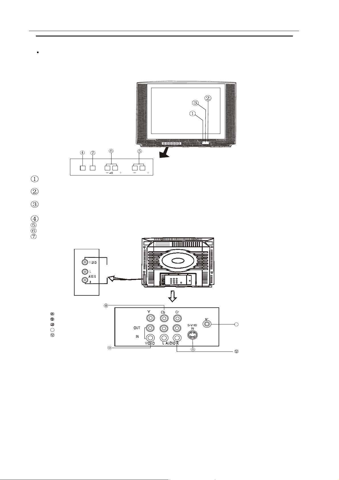
8 Parts and Funcitions
Front and side panel of the TV set
1 .Fro n t Pa n e l
MENUP TV/AV
Remot e sensor:let The remo te controller aim he re the set can rece ive remote
control signal.
Power switch:Press the button to turn on the TV set . press the button again to turn
off the TV set.
Power indicator: the indicator lights in standby status ,the indicator lights in sleep
status . The indicato r glin ts when you use remote contro ller
Menu butto n
Progr am up/do w n button
Vo lu me up/down button
TV/AV
2.Rear Panel
And Side Board
.
Parts and Funcitions
VIDEO input
Left audio input
Right audio input
S-VHS input
VIDEO input/output
DVD component input
11
Antenna input
Audio input/output
A V IN 1
When using S terminal, please pull out video 1 input terminal
Figure 2
11
12
Page 14

9. Remote Controller Functions
Remote Controller Functions
MARK
FUNCTION DESCRIPTION
Program scan
Standby
SWAP
Mute
1
2
3
TV/AV
-VOL+
-CH+
TV/VIDEO SELECTION
VOLUME CONTROL
CHANNEL NUMBER UP/DOWN
PICTURE MENU
P
.
P
C
P
I
T
R
U
E
S
W
P
A
SOUND
TIME
FUNCTION
0-9
SOUND MENU
TIME MENU
FUNCTION MENU
ONE DIGIT SELECTION
-/--
MENU
MENU DISPLA Y
EXIT MENU DISPLAY
STEREO/NOMO SOUND SE LECT I ON
PICTURE MODE SELECTION
SOUND MODE SEL ECTION
TUNE MENU SELECTION
CHILDLOCK
Figure 3
13
Page 15

Program Diagram
10.ProgramDiagram
OPERATION MENU
OCT
TUNE
COLOR SYSTEM AU T O
SOUND SYSTEM B/G
BAND VHFL
SKIP OFF
PROG NO 19
SEARCH
FINE TUNE
AUTO SEARCH
6.Selecting color syste m
Usually this should be set in the Auto position. However if the colours displayed on
the scree n are incorrect you can manually select the correct co lour sy stem. When
you have f inished remember to turn it back to auto ag ain so that other pro g rams
will still work correctly. Use the CH+/- buttons to select COLOR SYSTEM then the
VOL+/- buttons to select a color system you need.. Press the EXIT button to save
the setting.
14
Page 16

Program Diagram
OPERATI ON M ENU
7.Program skip
The Program ski p featur e enables you to sk ip /h id e program s th at you do n o t w ish to
be displayed w hen usi ng th e C H + /- buttons. T h e se c h an n e ls w ill st i l l be di spl ayed by
di rect l y usi ng t he channel num ber but t ons on t he rem ote c o n tro l. th e
T o sk ip , press
CH+/- but t ons t o se lec t th e SKIP m enu, Pr ess the V O L+/ - but t ons t o t une t he skip
f eat ure on/ off. Pr ess the EX IT but t on t o save the setting .
8. Pr ogr am Number
The program num ber i s th e rem o te control channel num ber . Y ou can change th e
program num ber to see w hich channels are st ored w i t hout ex itin g th is m a in
menu. Pr ess t he CH +/ - but ton to se le c t PROG NO, Pr ess t he VOL+/- t o change
t he program num ber t hat you are adjusting.
9. Ba nd Sw itching (note: Thi s is a new item )
If you already know w hat band t he channel is on, t uning can speed up by
se lecting the correct band before going in to th e search menu. This feat u re
should only be used i f you underst and th e channels in your lo cal area.
Picture Adjustments
1 Contrast ( A dds dept h t o t he pictur e)
Pr ess t he CH+/- but t ons t o sel ect Contrast, th en
press th e V O L + /- b u tto n s to adjust t he Contrast l evel .
2 Bri ght ness (A dds sparkle and shine to the picture)
PIC T UR E
CONTRAST 89
BRIG HTNESS 66
COLO UR 50
SHA RPN ESS 50
TILT 08
IIIIIIIIIIIIIIIIIIIIIIIII..........
OCT
Pr ess t he CH+/- but t ons t o sel ect Brightness, then
press th e V O L + /- b u tto n s to adjust t he brightness
lev el.
3 Col our (A dds col our dept h)
Pr ess t he CH+/- but t ons t o sel ect Colour, then press t he V O L + /- but t ons t o
adjust th e C olour l evel .
4 Sharpness (A dds fine detail)
Pr ess t he CH+/- but t ons t o sel ect Sharpness, then press t he VOL+/- but tons t o
adjust th e Sharpness le v el.
Note: D o n o t tu rn th e sharpness up to high if th e rec e p tio n is poor or has l ots of
noi se as it w ill enhance t he fine g rain details.
15
Page 17

OPERATION M ENU
Sound Adjustments
Press th e m e n u b u tto n tw ice or press the Sound button on th e rem o te con trol,
to display th e Sound setting m enu.
1 Volum e (A djust the l oudness l evel )
SOUND
VOLUME 50
BASS 50
TR EBL E 50
BALANCE 0
SURROUND OFF
WOOFER ON
WOOFER VOL 50
IIIIIIIIIIIIIIIIIIIIIIIII..........
OCT
Pr ess t he C H + /- b u tto n s to sele ct Volum e,
th en pr ess the VOL+/- but tons to adjust th e
v o lu m e lev el.
2 Ba s s (Add lo w frequency depth)
Pr ess t he C H + /- b u tto n s to sele ct B ass, th en
press th e V O L + /- b u tto n s to adjust t he
v o lu m e lev el.
3 Tr eble ( Add hi gh f requency clarity)
Pr ess t he C H + /- b u tto n s to sele ct Treble, th en
press th e V O L + /- b u tto n s to adjust t he treb le
lev el.
4 Balance (S elects betw een the left and righ t
stereo channel l evels)
Pr ess t he C H + /- b u tto n s to sele ct Balance,
th en pr ess the VOL+/- but tons to adjust th e
balance lev el.
5 S urrou n d (E nh ances the stereo effect by
m aki ng t he sound appear w ider)
Pr ess t he C H + /- b u tto n s to sele ct
SURROUND, th e n press t he V O L+/- but t ons
to tu rn th is fea tu re on/off.
6.W oofer on/off
Press the CH+/- buttons to select
SURROUND, then press the VOL+/buttons to turn this woofer on/off.
7.Woofer volume adjustment
Press the CH+/- buttons to select
WOOFER VOL, then press the VOL+/buttons to adjust woofer volume.
16
Page 18

OPERATION MENU
Function Menu
1.B ackground (If th e sig n a l is very poor or t here is no
in pu t signal th e picture w ill m ute to black)
Pr ess t he C H + /- but t ons t o sel ect Background,
th en pr ess the VOL+/- b u tto n s to tu rn th is feat u re
on/off.
FUNCTION
BACKGROUND ON
BLACK STR ETCH ON
NOISE REDUCE OFF
FA D E ON
CHILDLOCK OFF
AV L OFF
SO FT CHANGE OFF
OCT
2.N oise R educe (P icture Noise & G rain reduction c irc u it.)
Pr ess t he C H + /- but t ons t o sel ect Noise Reduce, th en press t he VOL+/but t ons t o t ur n th is feature on/off.
4. Chi ld Lock (Enables th e TV front cont rol but t ons t o be lo ck ed )
Pr ess t he C H + /- b u tto n s to se lec t C h ild L o ck , t hen press th e VOL+/ but t ons t o t ur n t hi s feature on/off.
5. AV L (A ut om at i c Volum e Li mit control reduces effect of l arge vol um e
changes such as w hen the ads com e on) Press th e C H + /- b u tton s to select
AVL, th en p re ss th e VOL+/- buttons to tu rn th is featu re on/off.
6. B lack Stretch (A dds D eeper B l acks and i ncreases the contrast range)
Pr ess t he C H + /- but t ons t o sel ect Black Stretch, th e n press t he VOL+/- buttons
to tu rn th is fea tu re on/off.
Calender Menu
E n ter C a len d e r m e n u , press th e P+/P- to sel ect year, month, dat e, press th e VOL+/to cha n ge calender set up.
SOLA R 2008 1 20
LU N A R 2002 12 18
S M T W T F S
1 2 3 4
5 6 7 8 9 10 11
12 13 14 15 16 17 18
19 20 21 22 23 24 25
26 27 28 29 30 31
17
Page 19

MULT I FUNCT ION TIM ER
Multi Function Tim er
The TV set has in built a c om p reh en siv e tim er
th at has Five basic funct i ons
1.Clock
2 .O n tim er so th a t the TV set can be pr ogram m ed
to tu rn o n at a certain t im e
3.O ff tim e r that allow th e TV set to tu rn off at a
preset tim e
4.Sleep t im er to allow t he T V se t to tu rn o ff after
TIM E
CLOCK --:-ON TIM E --: -ON-PROG 1
OFF TIM E --:-SLEEP TI MER --: -REM IND TIM E --:-REM IND PRO G 1
COUN T 00001:22
OCT
10 ~ 180 minutes
5. Program r em ind t i m er , that displays an onscreen rem inder prom pt, when a program on a
di fferent channel i s due to star t.
Note: The clock w ill o nly wo rk if th e T V set if le ft tu rn e d on or in standby.
W hen the set is disconnect from th e p ow er supply or i s turned of f by t he
main pow er sw itch o n th e fro nt panel, th e clock lo o ses pow er and w il l
need to be re se t w h e n th e pow er is reconnected.
18
Page 20

MULTI FU NCTIO N TIM ER
to a d ju st th e am ount of t im e before th e TV se t w ill a u to m atic ally
tu rn o ff. Each tim e th e V O L+ but t on i s pressed the sleep tim e will in c re ases by 10
minutes. The m axi m um sl eep tim e i s 180 m i nut es.
5. Remind Tim e
Press th e C H + /- buttons to select R E M IN D TIM E, then press the VOL+/- but t ons t o
adjust th e H ours
Press th e C H - Button to sele ct min utes an d th e VOL + /- to a d ju st th e minutes.
Press th e C H - Button to sele ct REM IND-PROG and the VOL +/- to select the TV
channel th a t the T V set w ill au to m atically rem ind you to t ur n t o w hi l e wat ching
another channel.
6.C ount
The funct i on i s used for di splay t he TV s et used for all tim e.
OCT
Program Number E xchange
This fe ature enables TV program s that m ay
be on a wrong TV channel num ber to be
sw apped/exchanged. This feature is very
EX CH A N G E
P ROGRAM 1 1
P ROGRAM 2 1
EX CH A N G E
usef ul w hen A utom atic Search Tuni ng has
been used, to re allo c a te t he found program s
to th e co rrect channel num ber s.
Pr ess t he Menu butt on 6 tim es unt i l t he exchange m enu i s displayed.
Pr ess t he CH+/- until program 1 is selected. Use th e VOL+/- buttons to
select the channel num ber to be sw apped. (I. E if you wi sh to exchange
Cha nnel 2 and 4 PR O G RA M 1 shoul d = 2)
Pr ess t he CH+/- until program 2 i s selected. Use the V O L+/ - but tons to
select the channel num ber to be sw apped. (I. E if you wi sh to exchange
Cha nnel 2 And 4 PRO G RA M 2 shoul d = 4)
Pr ess t he CH+/- until EXCHANGE is sel ected. Pr ess th e VOL+ button to
enable t he exchange.
19
Page 21

GENERAL OPERATION
1.C hannel Changi ng (218 possibl e channels)
Use either th e C H + /- buttons on th e rem o te o r th e f ront of t he TV s et to change t he
channels.
Or
D irect ly ent er t he channel num ber w i t h t he num eri c keypad on th e rem o te co n tro l.
To sel ect channel num ber s from 10 ~ 99 press [-/--] button an d enter th e tw o digit
channel num ber. To sel ect channel num ber s from 100 ~ 218 pr ess [-/ --] button
tw ice and enter the 3 digit channel num ber.
2.Volume Adjustment
Press th e V O L + /- b u tto n s on th e re m o te o r th e fro n t of th e TV se t to ad ju st th e
vol um e le v el. The range i s 0~99. W hen the Vol um e but t ons are pressed the volum e
l evel i s di spl ayed autom atically on th e TV scr een.
3.Standby
U sin g th e rem ote cont rol t he TV s et can be pl aced i nt o standby mode. Standby
m ode m ust be used fo r th e Tim er features to operate correctly. A re d standby lig h t
w ill g low on th e TV front panel when th e T V set is p la ce d into standby. To tu rn
th e TV set back on agai n pr ess st andby but t on on t he rem o te control again. It will
take a few seconds before a picture w ill be displayed.
4.Mute
Press th e m u te button on th e re m o te co n tro l to mute th e TV set s sound. Pressing
th e M ute again w ill tu rn th e sound back on again.
5.Preset Picture M odes
Our engineers have desi gned i n 5 com m onl y used pi ct ure set ti ngs to allow fast
pi ct ure lev el selectio n depending on w h a t ty p e o f TV program is show ing. Each
m ode i s se lec te d in tu rn by pressi ng t he "P STD " button on th e rem o te co n tro l.
The 5 modes are
Listen- This is a new feature th at blacks out th e TV screen when listening to
music onl y channel s
Soft - D esigned for night tim e l ow l i ght vi ew i ng
Standard - D esi gned f or room s th at have good all round l i ght i ng
Rich - D esigned fo r room s w i th hi gh am bi ent l i ght i ng such as daytim e sport .
User- A s pare setting th at can b e ad ju sted t o personal tastes
U sin g th e PICT URE adj ust m ent di splay m enu all 5 m odes can independently
adjus ted.
20
Page 22

GENERAL OPERATION
6.Pr es et Sound Modes
Ou r engi neer s have designed in 4 com m only used sound mo des to allo w th e
best possi bl e sound t o be selected quickl y. Each m ode i s sel ected in tu rn b y
pressing t he "S STD" but ton on th e rem o te control.
The 4 m odes are
Speech- D esi gned to red u ce th e bass and tre b le w hi ch enhances th e voice fo r
Ne ws program s
Theatre- Enables extra bass and treble to enhance t he m ovie exp erience
M usi c- Adjust the sound to best suit m usic program s
U ser - A s pa r e settin g th at can be adj ust t o per sonal t astes
U sing th e SOUND adjustm ent display m enu all 4 m odes can independent l y adj ust ed
7. Recal l ( O n-screen Display)
The Call butt on on the rem ote control allow s the onscreen menu to be
displayed, show ing th e channel num bers and col our syst em .
8. Program Scan (A ut om at i call y in c rem en ts/scan s th e channels and displays
each channel fo r a sh ort tim e)T he SC A N butt on on t he rem o te control turns
on/off th e scan f eature.
9. Zoom (Changes th e p ictu re si ze form at)
Each tim e the ZOOM b u tto n is pressed th e p ictu re si ze w il l change. There
are th e foll o w ing size options.
Normal - Used fo r st andard 4: 3 picture program s
E nlargem ent - Z o o m s th e p ictu re in to magnify sm aller im ages.
10.Sw ap (Toggles betw een the last channel view and the current channel)
Each tim e th e SW AP butt on i s pressed the last channel view i s di spl ayed.
11.AV input sel ect i on
Each tim e the TV/AV but t on i s press t he inp u ts selectio n will cycle betw een
TV- AV1- AV2- SVHS- DVD - TV.
No te s: I.AV1 & SV HS share the sam e AV 1 audio inputs.
.In AV m odes the RECALL stat us di spl ay will o n ly di spl ay t he colou r
system .
12.Lock
Pr ess t he LOCK b u tto n to sele ct Chi l dl ock on/ off.
21
Page 23

Maintenance Service and Trouble Shooting
11. Maintenance Service and Trouble Shooting
a. TROUBLESHOOTING PROCESS
Grating off
Check +B
Abnormal Normal
Disconnect R214 to
check main voltage
Normal
Abnormal None
Check TDA9373
voltage
Check for short between
output voltage and ground
Check for 300V voltage
Check N801 for
peripheral circuit
Check R415, R505
and R526
Check V403, T401
Check V402
Check pin 33 of
N201 for output
Check lamp filament,
release and grating voltages
Check CRT
cathode voltage
Check N201 for
signal output
Check TDA6107Q
and peripheral circuit
R, G and B
22
Page 24

d
Maintenance Service and Trouble Shooting
Horizontal bright line
Check pin 21 and 22 of N201 for curve output
None Yes
Check R228 and C227
Abnormal Normal
Check N201
Check R413 and R408
Check T444
Check 16V and 47V
voltage
Check N301 an
peripheral circuit
Disabled remote control
Abnormal Normal
Check all pins of V801for voltage
Check receiver voltage
Check pin 61 of
N201 voltage
Check RR230 and C234
Check VD806 for
voltage output
Check receiver
Check N201
23
Page 25

Pincushion distortion
Maintenance Service and Trouble Shooting
Enter factory mode and adjust
5EWP to see if picture changes
None Yes
Check pin 20 of N201for voltage
and ground resistance
Check
V401 and DZ401
Check pin 12 N301 for voltage
and ground resistance
Check C416
Check and replace
N201 and N301
Check and replace
VD404A andVD404B
24
Page 26

Maintenance Service and Trouble Shooting
TV program sound off
Yes
Check pin 7 of N201 for
None Yes
Yes None
noise suppression
No
Check N201 44 for
sound signal output
Check and replace N201
Check N701 3 5
for sound signal output
Check N701 15 18
for sound signal output
None Yes
Check and
replace N701
Check N601 and peripheral
Press mute button, or check
and replace N201
Check V213, R243,
C246 and C706
circuit components
25
Page 27

Maintenance Service and Trouble Shooting
b. Troubleshooting guide
To assist in location possible faults use help guide below
BREAKDOWN PHENOMENON
PICTURE
Picture with snow Noise
Double or Triple Image
Disturb
No Picture No sound
SOUND
Normal
Noise
No soundNormal
The aerial direction and connection
This is called ghosting which can be minimized with
an outside aerial, and good quality cable and
terminations. Altering the aerial direction can also
minimize this effect.
Electrical interference which can be caused by cars,
motorbikes etc, Fluorescent lamps and dirty
insulators on overhead power cables.
Volume Sound mute
Ensure that the power supply is connected to
the TV set and turned on. Also ensure that the
TV set is not in "Listen Mode" or that the
brightness and contrast are not turned down.
CHECKING
.
Adjust colour control
No colour Normal volume
Adjust channel again
Scramble
Colour Spot
Note:
1.If the fault can not be repaired using the above guide consult with your local authorized service
center.
2.The TV set must only be repaired by a qualified registered service person. Never attempt to
remove the back cover as the TV set has dangerous voltages in side that may cause a fatally or fire.
3. The cabinet may produce the occasional "snapping sound" This is normal and caused by the
materials in the cabinet expanding with room temperature changes.
Normal or Weak Volume
Normal volume
Colour Purity fault which can be caused by moving the
TV set, placing magnets near the TV screen or turning
on/off house hold appliances such as vacuum cleaners
near the TV set. Turn the TV off with the mains power
switch for 15 minutes. When the power is turn on again
the TV set will automatically degauss the picture. In
server cases leave the TV set turned off over night.
26
Page 28

p
g
p
12. Circuit Diagram
Circuit Diagram
a. Pane hint picture
b.
+8V
RM201
remote
control
TU101
TUNER
SCL
E2PROM
Assistant
power supply
Switch
transforme
Microprocessor and signal processor
r
SF101
sound surface
filte
SDL
SDL SCL
+5.1V
+130V
+16V
+15V
r
Dark current
check-u
N201
The second SIF filter
The second SIF WAVE TRAP
V-SYNC
H-SYNC
pillow figure
emendation
N701
Sound processing and
lifyin
am
MUTE
peaker1
CRT
+46V
+16.5V
+200V
S
Speaker2
N610
Sound
amplifying
N501
Video frequency
amplifying
N301
field output
V403
line output
tube
T444
FBT
R
G
B
V
-DY
H-DY
FOCUS
SCREEN
Figure 4
27
Page 29

c
Circuit Diagram
Circuit Diagram
P+
P-
TV/AV
V-
V+
RB03
1.8K
TU101
ENV59D69F1Q
VT B U
AGC
C105
C107
C106
104
22U
0.33U
R110
51
L103
10uH
R261
12K
VD217
1N4148
R203
R202
10K
11K
C203
104
BL
BU
V204
KSR1010
C212
104
BH
CN801
TJC1-2Y
L801
LCL-207
CN802
TJC1-2Y
RP803
PTH
DEGUSS
VD810
D5SB60
1234
+
C804
222
~~
RP801
5
C805
222
MENU
TJC3-2Y
1
RB06
1.2K
C104
104
L102
10uh
9.1K
R262
R227
100
R260
9.1K
R204
10K
C204
104
C210
104
C213
104
C211
104
SW07
KDC-A10
C801
104
R801
3.3M
DV801
MYN15-471K
R803
33K
R802
33K
R804
470K
C806
330uF
R805
470K
RB09
CNB01
620
1K
470
TJC3-2Y
2
R219
R222
R220
R212
R223
A6-5V
3.3K
3.3K
3.3K
3.3K
AFT
NC
NC11IF
+BBH BL
GND
9
1083154672
C101
0.22U
M9911AN101
C103
104
C102
220U
R102
2.2K
R103
2.7K
R201
10K
V201
4A/250VF801
123456
DZ102
MTZJ5.1B
L101
R101
1.2uH
24
B4-12V
C109
DZ101
103
MTZJ9.1B
CD108
47U
C110
102
VD101
SF101
K2972M
BAW75
R105
56K
R104
560
V101
BC548
C201
C202
DZ201
10u
104
KA33V
A1-33V
R206
10K
KSC815
C205
152
C206
R205
151
10K
V202
KSR1010
V205
R225
KSC815
10K
R224
10K
V203
KSR1010
LD901
HTRYG9208
KA5Q1265RF-YDTU
N801C
L803
L807
4
VFB
F/B
F/B
1
C807
2
222
VCC
SYNC
35
R806
VD804
470
IN4148
R807
C811
600
392
VD803
VD802
ERB4304
B1206
C808
47u
N802
PCT817C
C809
473
3.3K
STANDBY
R209
100
SCL
C209
R210
100
SDA
A5-3.3V
R266
3.3K
R216
47
C259
3.3K
SYSTEM
R218
MUTE
10K
MAG
C215
104
C214
104
224
L201
0.47uH
C216
.
A7-8V
L202
C219
C220
10uH
104
100u
C217
224
C218
222
R226
C222
15K
1u
C221
472
C224
2.2u
222
C225
C226
222
R228
39K
C227
104
C228
L204
L205
L203
223
1uH
1uH
1uH
C229
332
C230
10u
R229
3.9K
C231
102
C232
331
C233
EW-DRI
C813
472
R808
4.7M
4
3
4.7
VD-NVD-P
N804 KA7630
A7-8V
A5-3.3V
R841
R840
1K
1K
1234
C829
C828
10U
R821
220U
R820
1
1
R843
2K
V801
KSC815
C812
472
DZ808
CD842
MTZJ3.9B
10u
R809
C814
4.7M
L805
561
5.1
VD805
L804
T801
D5L60
BCK-100-02
LB3.5*5
1
8
C817
561
15
4
10
11
VD806
TR5GU41
6
VD807
L806
L808
12
D6L20U
LB.6*6
LB3.5*6
13
7
C519
561
14
1
R813
R845
1.5K
68
C821
R814
104
1K
2
DZ805
KA431
VD815
1N4148
R846
10K
RLP1
LK1aF-12V
V802
KSC815
CNB02
RB07
RB08
SDA
A6-5V
R211
R215
3.3K
3.3K
TDA9384PS/N2/3
N201
1
64
STANDBY
INT.REM
2
63
SCL
AV/SVHS
56
3
62
SDA
AV1/AV2
C208
56
461
VT
VDDP
5
60
RESET
KEY
6
59
SYSTEM
XTAL.OUT
7
58
XTAL.IN
MUTE
8
57
OSC.GND
MAG
9
56
VDD.C
VSSC/P
10
55
VPE
BAND
11
54
VDD.A
BAND
53
12
VSSA
B.OUT
13
52
SEC.PLL
G.OUT
14
51
R.OUT
VP2
15
50
DECD/G
BLK.IN
16
49
PH2.LF
BCL.IN
17
48
PH1.LF
B2/U.IN
18
47
GND3
G2/Y.IN
C223
104
46
19
DEC.BG
R2/V.IN
20
INSS.W2(BL)
EWD
44
21
AUD.OUTV.DRB
43
22
CHROMA
V.BRA
23
42
CVBS/Y
IF.IN1
24
41
GND1
IF.IN2
25
40
CVPS.INT
I.REF
26
39
VP1
V.S.C.
27
38
IF.VO/SVO
AGC
28
37
PLL.IF
AV.DEEM
29
36
EHTO
DECS.DEM
30
35
AUO.EXT
GND2
31
34
F.B.L.SO
SND.PLL
324533
H.OUT
AVL
56 78910
VD810
C831
R822
10U
10K
IN4148
C830
DZ803
1U
5.6B
7.5KR811
C816
R817
100u
33K
C815
220u
C818
2200
C820
2200u
R815
R849
127K
10K
R824
39K
VD816
1N4148
R816
R848
R847
2.49K
6.2K
6.2K
DZ807
MTZJ5.1B
V206
KSC815
SCL
R208
A6-5V
N202
100
24C08
A6-5V
RM201
1
8
E0
VCC
C207
HS0038A
103
E1
WC
E2
SCL
R943
GND
SDA
OUT
GND
VCC
47
4
5
R230
100
C234
102
AV/SVHS
AV1/AV2
C236
22U
X201
12M
C242
104
R238
12K
R248
6.8K
C250
10u
BL
C246
10U
C247
474
C253
474
C255
100U
R244
390
C256
R276
27K
104
R245
100
R263
200
H-DRI
A6-5V
A7-8V
C832
100U
C833
47U
POWER
A5-3.3V
A3-15.8V
A1-33V
10KR810
A2-130V
A3-15.8V
A4-15V
A6-5V
V803
KSC815
R214
10K
C922
100U
A6-5V
L206
10uH
C237
104
C239
33
C240
33
L207
10uH
L208
10uH
C241
100uH
D-COIL
A5-3.3V
R235
100
R236
100
R237
100
VD201
R274
IN4148
22K
R273
33K
R277
100K
R264
470
R265
75
C248
VD202
104
IN4148
H-SYNC ABL
A7-8V
A7-8V
V213
KSC815
R262*
4.7K
R255
430
R250
47
V209
KSC815
V208
KSC815
DZ205
MTZ4.7B
R249
20K
R710*
4.7K
R242
1K
R243
1K
R256
470
L209
10UH
C254
223
R275
270K
R259
100K
R246
8.2K
C249
151
R247
3.3K
R213
10K
POWER
ST-BY
N702
HEF4053
9
8169
CN201
10
10
11
11
R740
R741
3.3K
3.3K
12
12
C744
13
13
1u
14
14
15
15
16
CVBS/Y
R742
10
AV1-AL
AV1-AR
R708
220
L708
10uH
C705
C725
224
224
BASS
32 31 30 29 28 27 26 25 24 23 22 21 20 19 18 17
N701
TDA9860
B-OUT
G-OUT
R-OUT
12 3 4 5 6 7 8 910111213141516
D-COIL
CUT-OFF
L709
10uH
21P-B
21P-G
21P-R
L211
10uH
C252
47u
Z203
4.5MHz
R254
180
Z204
5.5/6.0/6.5MHz
R253
L210
510
5.6U
Z201
R252
5.5MHz
100
Z202
R251
5.5/6.0/6.5MHz
200
TJC-2A
7
6
Y-SVHS
R719
100
AV1-VIN
5
4
R718
75
3
R715
2
75
Y
1
AV2-VIN
AV2-AL
AV2-AR
R707
R704
R703
220
220
220
L704
L707
L703
10uH
10uH
10uH
C721
C727
C723
C722
224
153
153
224
VI4P2VO2 CPS1 VI1 CPS2 VO5 MAD VO1 VI7 CBL1 CBL2 VO7 CTL VO3 SDA
HEADPHONE
CHANNEL
MULTIPLE
VOLUME
SOURCE
AND MODE
SELECTION
CROSS BAR
SWITCH
REFERENCE
VOLTAGE
CONTROL
VI3 P1 VI 5 CSMO
VP VO5 VO2 VI2
VI6
C707
100u
R751
C708
R752
SHORT
10K
10K
C710
C709
C706
100u
104
224
R-OUT
A-OUT
A-OUT
C-SVHS
Y-SVHS
A7-8V
V210
R257
KSR2010
47
C257
47u
V212
V-OUT
KSC815
R258*
R258
75
1K
V211
KSR1010
SYSTEM
A7-8V
AV1-VIN AV1-AL AV1-AR
CNS01
CT0175RT01
102
RT03
RT02
YC
75
100
CNT01
TJC3-10A
CN200
C-SVHS
YCbCr
R-OUT
L-OUT
V-OUT
AV2-VIN
AV2-AL
AV2-AR
L-OUT
R706
100
R731
R730
10K
1K
C720
10u
STEREO
SPATIAL
STEREO
PSEUDO
STEREO
FORCEO
VOLUME
MONC
GND
R726
C711
1K
10u
R727
10K
R705
100
SCL
SDA
HEATER
B1-180V
R602
0.18
A4-15V
V04
POWER
mute
V03
CN701
AV1-VIN
OUT
VIDEO
C718
333
C719
10u
BASS
TREBLE
CONTROL CONTROL
CBR1 CBR2 VO6 CTR VO4 SCL
C712
10u
C713
333
V05
CNS02
AV1-AR
AV1-AL
C001
10u
CN001
TJC3-4Y
C002
10u
C003
R001
R002
10u
120
120
R003
120
C717
562
IIC-BUS
CONTROL
HUE
VOLUME
BALANCE
C714
R728
R729
562
100
100
R610*
6.2K
R741
R740
R611*
100
100
6.2K
V04 V03
VD-P
VD-N
EW-DRI
H-SYNC
B4-12V
A3-15.8V
H-DRI
A2-130V
HEATER
B1-180V
ABL
C507
C508
391
391
CN501
CN503
R507
TJC-5
100
1
G-OUT
R508
100
B-OUT
2
R509
GND
CUT-OFF
CN502
TJC-3
HEATER
1
180V
2
3
INPUT INPUT
12345678910
2.3V 2.3V 8.5V 17.3V 8.4
R301
3.3K
V402
KSC2331-Y
100
3
4
5
R505
2.4
6
7
R526
68
8
C502
222
C506
10u
R527
33K
R601
0.18
DZ604
MTZJ30D
N301 TDA8350Q
VERTICAL
FEEDBACK
GND
VP
NC VFLYBACK OUTPUT
R302
1.5
C303
R303
68u
1.5
C302
C301
100u
474
DZ301
MTZJ22A
C306
104
VD301
1N4148
DZ304
MTZJ30D
DZ306
MTZJ30D
C421
100u
C422
104
VD403
IN4004
VD402
IN4004
R411
C412
110
T401
561
R410
270
C413
100u
C411
103
C509
391
MTZJ9.1B
DZ501
MTZJ9.1B
15 14 13 12 11 10 9 8 7 6 5 4 3 2 1
L601
10uH
R304
33K
N401
KA7812A
C426
100u
R415
0.39
DZ504
DZ503
MTZJ9.1B
VD502
ERB4304
N601
TDA7297
OUT2 VCC2 SVR
C607
1000u
DZ603
MTZJ30D
L603
10uH
EASTWEST AMPLIFIER
C304
104
DZ303
MTZJ15C
DZ302
MTZJ30D
DZ402
MTZJ5.1B
R408
10
B2-46V
L304
33uH
C410
68u
B3-18.5V
C420
224
V403
FJAF6810D
C427
R421
33
GT501 1P
GT502 1P
R503
1.8K
R501H
1.8K
R502H
1.8K
3.0
3.0
3.0
DZ502
MTZJ9.1B
6.0
180
R510
100
111
R512
100
116
R511
100
114
VD503
VD504
ERB4304
ERB4304
ST-BY IN2 MONO
IN-MUTE
C605
1u
C606
103
R606
3.3K
R607
6.2K
OUTPUT
INPUT
INPUT
12
13
11
0.7V47V 8.7V 13V
R403
5.6K
R401
52.6K
R402
100
V401
KSA614Y
DZ401
MTZJ30D
R407
3.9K
C409
471
C408
472
VD407
ER24-06
VD405
R414
R5GU41
10
C418
471
C419
470u
C414
VD404
FMP-3FU
472
102
C503
103
SC
FO
HV
N501B TDA6107Q
123
V1 V2 V3 VDD
1
GND
456789
2
3
PROBE3
PROBE2
PROBE1
GND
C604
DZ605
102
MTZJ5.6B
POWER
C402
103
L401
1mH
C403
22u
C407
681
R413
0.27
C415
752
R415
C416
0.47
153
CRT
73X707Y22-DC01
R504
10M
C504
4.7u
VD501
ERC24-06
IN1
MUTE1
VCC1 OUT1
SPEAKER2
CN602
TJC3-2Y
CN603
VD601
IN4148
C603
2.2u
R605
1K
VD602
IN4148
MUTE
L301
10uH
R305
R306
390
220
L302
10uH
C406
474
VD401
C405
TR5GU41
2.2u
18K
R406
R405
390
L402
AC0031TL
C404
102
T444
JF0101-85907
8
46
9
16.5
6
7
HEATER
1
H-OUT
4
5
VIDEO
3
B+
VD406
TVR10G
R417
91K
SPEAKER1
C601
TJC3-2Y
1u
R604
R603
6.2K
3.3K
C602
103
DZ601
DZ602
MTZJ30D
MTZJ30D
C305
104
V1
V2
CN401
TJC-4
H2
H1
TO CRT
HV
HV
FO
SC
FO
SC
TO CRT PCB SCREEN & FOCUS
10 11
C423
471
C424
C425
R419
22u
104
1K
R418
GT404
91K
NOTE:This diagram is only for reference and subject to
28
Page 30

Circuit Diagram
c.
PCB Diagram
Figure 6
29
Page 31

Circuit Explanation
13. Circuit Explanation
The UOC module comprised of Philip super advanced CMOS chip TDA9373 is used for model
34F9B-T color TV pictures and text. This product has I2C bus-mastering digital control system and
DVD component terminals (or SCART terminal) for auto sound identification, independent woofer
volume control, English and Russian picture texts, treble and bass tone increase, image and sound
mode for individual preference, picture size zooming and 218 channel storage.
I. Electrical circuits and integrated circuits of 34F9B-T TV receiver
1.1 Electrical circuits
Electric circuits of the 34F9B-T TV receiver are comprised of the following sections:
1.1.1 Microprocessor and signal processor: comprised of super single chip integrated circuit
N201(TDA9373), storage N202 (KS24C08).
1.1.2 Sound processing and amplifying: comprised of integrated circuit N701 (TDA9860) for
sound tone processing and integrated circuits N601 and N610 (TDA7297) for sound
amplifying.
1.1.3 Integrated circuit for line and field scan output: comprised of integrated circuit N301
(TDA8350Q) for field output, V403 (2SD1887YD) for line output tube and T444
(BSC29-0130D) line output transformer.
1.1.4 Video frequency amplifying: comprised of integrated circuit N501 (TDA6107Q)
1.1.5 Power supply control: comprised of switch transformer T801 (BCK-100-02), power
integrated circuit N801(KA5Q1265RF-YDTU) and secondary power integrated circuit N804
(KA7630).
1.2 Main integrated circuits:
1.2.1 TDA9373 Microprocessor / picture intermediate frequency / sound intermediate
frequency / video processing / line field scanning / color decoding / text
1.2.2 TDA9860 Multi- function TV stereo sound tone processing integrated circuit
1.2.3 TDA8350Q Field output integrated circuit
1.2.4 TDA6107Q Video amplifying integrated circuit
1.2.5 TDA7297 Sound amplifying integrated circuit
1.2.6 KA5Q1265RF-YDTU Power integrated circuit
30
Page 32

Circuit Explanation
1.2.7 KA7630 Secondary power integrated circuit
2 Electric circuit analyses
2.1 Super single chip integrated circuit TDA9373
As a super large-scale decoding and microprocessing integrated circuit, TDA9373 is comprised of a
microprocessor, picture image intermediate frequency amplification, sound intermediate frequency
amplification, line and field scanning, dwarf signal processing, color decoding, sound filtering and
auto identification, luminance separation, high voltage tracking and over voltage protection. It
functions for I
2
C bus-mastering and automatic adjustment for transmeridional correction and dark
balance.
Table 1 lists the pin function and test data of TDA9373 as the reference for maintenance.
The data is to be tested under the mode of 49.75MHz, PAL B/G and cylindrical color card muting,
using a model FLUKE 79
instrument.
Table 1
Resistance to Ground
Pin Function
Working
voltage
V
Forward Test Back Test
R
1. STANDBY 0 36K 29K
2. SCL 3.5 15K 15K
3. SDA 3.2 15K 15K
4. VT 3.0 20K 20K
5. KEY 3.4 36K 30K
6. SYSTEM 4.4 15K 15K
7. MUTE 5.1 15K 15K
8. GND.MAG 0 Infinity 2.9M
9. VSS C/P 0 0 0
10. BAND 3.3 14.5K 14K
11. BAND 0 14.5K 14K
12. VSSA 0 0 0
13. SEC.PLL 2.3 6.4M 4.3M
14. VP2 7.8 18K 18K
15. DECD/G 5.0 31.9K 32K
16. PH2.LF 2.9 6.4M 4.2M
17. PH1.LF 3.9 6.4M 4.2M
18. GND3 0 0 0
19. DEC.BG 4.0 39.8K 40K
20. EWD 0.7 63K 63K
21. V.DRB 2.4 6.0M 4.0M
22. V.BRA 2.4 6.0M 4.0M
23. IF.IN1 1.9 37.5K 38K
24. IF.IN2 1.9 37.5K 38K
25. I.REF 3.85 38.8K 38.8K
26. V.S.C. 3.8 6.3M 4.6M
27. TUNER.AGC 1.7 4.9K 4.9K
28. AU.DEEM 3.2 6.1M 3.6M
31
Page 33

Circuit Explanation
29. DECS.DEM 2.4 5.9M 3.6M
30. GND2 0 0 0
31. SND.PLL 2.4 6.3M 4.7M
32. AVL 0 6.2M 3.8M
33. H.OUT 0.6 21K 21K
34. F.B.L.SO 0.3 6.4M 4.4M
35. AUO.EXT 0 0 0
36. EHTO 1.7 21.8K 22K
37. PLL.IF 2.4 6.4M 4.6M
38. IF.VO/SVO 3.3 4.3M 4.6M
39. VP1 7.8 18K 18K
40. CVPS.INT 3.9 5.4M 4.1M
41. GND1 0 0 0
42. CVBS/Y 3.3 6.2M 4.0M
43. CHROMA 1.5 83K 83K
44. AUD.OUT 3.4 6.4M 4.8M
45.
INSS.W2
BL
2.1 0.86K 0.86K
46. R2/V.IN 2.5 6.3M 4.5M
47. G2/Y.IN 2.5 6.3M 4.5M
48. B2/U.IN 2.5 6.3M 4.5M
49. BCL.IN 1.5 216K 239K
50. BLK.IN 4.9 28K 28K
51. R.OUT 2.8 7.46K 7.5K
52. G.OUT 2.8 7.48K 7.5K
53. B.OUT 2.9 7.5K 7.5K
54. VDD.A 3.3 32K 26K
55. VPE 0 0 0
56. VDD.C 3.3 32K 26.5K
57. OSC.GND 0 14 13
58. XTAL.IN 1.8 3.0M 2.7M
59. XTAL.OUT 1.7 0.5M 0.54M
60. RESET 0 0 0
61. VDDP 3.4 32K 26.6K
62. AV1/AV2 5.1 15K 15K
63. AV/SVHS 5.1 15K 15K
64. INT.REM 5.0 41K 40.6K
2.3 Analysis of common passage circuits
Having been received by antenna or fed by cable TV into the antenna input terminal of HF tuner
TU101
TECC7949 , HF TV signals pass through tuning for station selection, HF amplification and
frequency mixing inside the HF tuner and then, a 38MHz IF picture signal and 31.5MHz IF sound
signal will be transmitted from the IF terminal of TU 101 and be fed directly into (1) of the pre-IF
amplification thick-film circuit N101 (M9911A), where the signals will be amplified to compensate for
the insertion loss of the sound surface filter.
The sound surface filter SF101
K6264K adopts single-terminal or double-terminal input according to
different system choices. The single-terminal or double-terminal input are controlled by the (6) of
N201 via V101
BC548C : D/K, B/G and I signals will be input in a single channel and M signals in
double channels. The sound surface filter K6264K is a wide range filter for single channel input,
suitable for D/K, B/G and I sound signal; and is a narrow range filter for double-channel input,
32
Page 34

Circuit Explanation
suitable for M sound signal. The IF signals which have passed through sound carrier deep trap by
sound surface filter will be sent to the (23) and (24) of N201
be sent out from the (27) of N201
TDA9373 under the control of I2C bus for the gain control of HF
TDA9373 . HF amplification AGC will
tuner.
2.4 Analysis of signal trap option switch circuit
Video color signals will be sent out from (38) of N201
TDA9373 and emit and followed by triodes
V208 and
V209, and then, divided into sub-flows which are fed into the wave traps Z201~Z204 respectively. All
TV signals will be selected and pass through V210 and V211, which are rejector triodesand serve the
function of switches here. When the 6 pins of N201(TDA9373) export high level with sound below
4.5M, V211 will break over and the signals will pass through the wave traps Z201~Z202; and when
the 6 pins send out low level with sound of 4.5M, V211 will stop and V210 break over, and the signals
will go through the wave traps Z203~Z204. Video signals will be produced after all TV signals are
trapped by the wave trap, and then, one sub-flow will go through R255
430 and R256 470
for signal adjustment amplitude and enter into (40) of N201 TDA9373 , and another sub-flow will,
after emit and followed by a triode V212, serve as AV output.
Both the video signal in AV signals and the Y signal in S terminal signals will be selected and passed
through by N702
signal of S terminal will be fed into the (43) of N201
and the Y signal of S terminal will be selected and passed through by N702
control of the (62) and (63) of N201
The DVD component terminal Y, U and V signals will be coupled by the capacitors C001
HEF4053BP , and will then be fed into the (42) of N201 TDA9373 ; and the C
TDA9373 . Both the AV1 and AV2 video signals
HEF4053BP under the
TDA9373 .
10u ,C006
10u and C005 10u and fed into the (47), (48) and (49) of N201 TDA9373 respectively.
2.5 Analysis of sound tone processing circuit
The sound tone processing circuit is comprised of an integrated circuit N701
TDA9860 and
peripheral components. TDA9860 is a multi-function TV sound tone processing integrated circuit of Hi-Fi
grade, inside which treble and bass frequency division processing, stereo processing and encircling
sound processing are made.
The audio signals sent out by the (44) of N201, after emit and followed by V213 and passing through
a coupling capacitor C706
N701
TDA9860 respectively. Meanwhile, the audio signals from the left and right channels of AV1
terminal will be put into the (1) and (32) of N701
224 , will be divided into two sub-flows which enter into the (3) and (5) of
TDA9860 . The audio signals of S terminal and AV1
share the same sub-flow. The audio signals from the left and right channels of AV2 terminal will be
put into the (28) and (30) of N701
TDA9860 . The audio signals of DVD component terminal and
AV2 share the same sub-flow.
As for TV or AV audio signals that have been selected and go through inside N701 (TDA9860) without
sound tone processing, the independent audio signal of left and right channels and exported directly
33
Page 35

Circuit Explanation
from (13) and (20) will be directly fed into the (12) of woofer amplification integrated circuit N610
(TDA7297); and, as for the audio signals that have gone through sound tone processing , the audio
signals exported from the (18) and (15) will be directly fed into the (12) and (4) of the sound
amplifying integrated circuit N601
TDA7297 . The external capacitors C717 562 and C714 562
of the (19) and (14) of N701 TDA9860 are used as the treble control capacitors for left and right
channels. The (31) of N701
TDA9860 is a woofer control switch.
Table 3 lists the pin function and test data of TDA9860 as the reference for maintenance. The data is
tested under the mode of 49.75MHz
PAL D/K and cylindrical color card, using a model FLUKE 79
instrument.
Table 3
Resistance to Ground R
Forward Test
Back
Tes t
Pin Function
Working
Voltage
V
1 Pre-AV audio input of left channel 4.0 4.6M 3.1M
2 D-COIL 0.1 6.9M 4.9M
3 Interior audio input 4.0 4.7M 3.1M
4 Decoupling filter of power supply 7.9 9.1K 9.1K
5 Interior audio input 4.0 4.6M 3.1M
6 8V Power supply 8.0 2.8K 2.8K
7 AV audio output from right channel 4.0 6.5M 4.3M
8 Ground 0 0 0
9 Audio output from right channel 4.0 10.8K 10.8K
10 Audio input of right channel 4.0 4.6M 3.1M
11 Connecting terminal of bass control
4.0 4.6M 3.1M
capacitor
12 Connecting terminal of bass control
4.0 4.7M 3.1M
capacitor
13 Woofer frequency signal (L) 3.9 6.6M 3.9M~
14 Connecting terminal of treble control
4.0 6.2M 4.2M
capacitor
15 Audio output, right channel 4.0 8.8K 8.8K
16 Clock line of I2C bus 4.4 19K 17.9K
17 Data line of I2C bus 4.5 19K 18.0K
18 Audio output, left channel 4.0 8.9K 8.9K
19 Connecting terminal of treble control
4.0 6.2M 4.3M
capacitor
20 Woofer frequency signal (R) 3.9 6.5M 3.9M
21 Connecting terminal of bass control
4.0 4.6M 3.2M
capacitor
22 Connecting terminal of bass control
4.0 4.6M 3.2M
capacitor
23 Audio input of left channel 4.0 4.6M 3.2M
24 Audio output from left channel 4.0 10.8K 10.8K
25 Ground 0 0 0
26 AV audio output from left channel 4.0 6.5M 4.3M
27 Connecting terminal of analog. stereo
4.0 4.6M 3.2M
capacitor
28 Post- AV audio input of left channel 4.0 4.6M 3.2M
29 Connecting terminal of analog. stereo
4.0 4.6M 3.2M
capacitor
34
Page 36

30 Post-AV audio input of right channel 4.0 4.6M 3.2M
31 Woofer control 4.4 6.9M 4.8M
32 Pre-AV audio input of right channel 4.0 4.6M 3.2M
2.6 Analysis of sound amplifying circuit
The sound amplifying circuit is comprised of an integrated circuit TDA7297 and peripheral
components. TDA7297 is a double-channel stereo sound amplifying circuit featuring MUTE and
POWER functions, with power output 15+15W. TDA7297 has a BTL sound output manner with no
Circuit Explanation
coupling capacitor in its output circuit, which has a wide range of power supply
6V 18V and the
functions of short circuit protection and over-load protection.
(18) and (15) of the sound tone processing circuit N701 send out the sound signal for left and right
sound channels, which will be adjusted by R604, R603 and 607, R606 respectively , and then
coupled and fed into the (4) and (12) of the sound amplifying integrated circuit N601 via C601 and
C605, and , after being amplified, sent out from the (1), (2) and (14), (15) in positive and negative to
directly drive speakers for sound.
Woofer amplification is also comprised of the integrated circuit TDA7297 and peripheral components.
The sound signals from left and right channels that have not passed through sound tone processing,
will be coupled and fed into the (12) of N610 via C611, which, after being amplified, will be sent out
as positive and negative to directly drive speakers for sound.
Table 4 lists the pin functions and test data of TDA7297as the reference for maintenance. The data is
to be tested under the mode of 49.75MHz
79
instrument.
PAL D/K and cylindrical color card, using a model FLUKE
Table 4
Resistance to Ground R
Forward Test
Back
Tes t
Pin Function
Working
Voltage
V
1 Sound output from right channel 8.0 12.8K 12.7K
2 Sound output from right channel 8.0 12.8K 12.8K
3 15V Power supply 16.0 ~ 0.94M
4 Audio signal input of right channel 1.5 86.2K 86.6K
5 Blank pin 0 ~ ~
6 MUTE signal input 5.1 108.8K 107.6K
7 POWER signal input 5.1 5.6K 5.6K
8 Ground 0 0 0
9 Ground 0 0 0
10 Blank pin 0 ~ ~
11 Blank pin 0 ~ ~
12 Audio signal input of left channel 1.5 86.3K 86.5K
13 15V Power supply 16.0 ~ 0.94M
14 Sound output from left channel 8.2 12.7K 12.7K
15 Sound output from left channel 8.2 12.7K 12.7K
Table 5 lists the pin functions and test data of woofer TDA7297as the reference for maintenance.
35
Page 37

The data is to be tested under the mode of 49.75MHz PAL D/K and cylindrical color card, using a
Circuit Explanation
model FLUKE 79
instrument.
Table 5
Resistance to Ground R
Forward Test
Back
Tes t
Pin Function
Working
Voltage
V
1 Sound output from right channel 0 12.8K 12.7K
2 Sound output from right channel 0 12.8K 12.8K
3 15V Power supply 16.0 ~ 0.94M
4 Audio signal input of right channel 0 86.2K 86.6K
5 Blank pin 0 ~ ~
6 Bass signal input 4.4 108.8K 107.6K
7 POWER signal input 5.1 5.6K 5.6K
8 Ground 0 0 0
9 Ground 0 0 0
10 Blank pin 0 ~ ~
11 Blank pin 0 ~ ~
12 Audio signal input of left channel 0.7 86.3K 86.5K
13 15V Power supply 16.0 ~ 0.94M
14 Sound output from left channel 8.0 12.7K 12.7K
15 Sound output from left channel 8.0 12.7K 12.7K
2.7 Analysis of field output circuit
Field sync signals separated from the mixed sync signals trigger the field frequency division system.
Once a certain sum of field sync pulse signals have been detected, the field frequency division
system will start in action. Of the field sync pulse signals which are obtained from frequency division,
one sub-flow will be fed into a sample pulse generator to, together with line feedback signal, produce
sample pulses necessary for the circuit.
Another sub-flow will be sent to field saw-tooth wave generator. The field frequency saw-tooth wave
that has undergone geometric processing will be sent from the (21) and (22) of N201 to the (1) and (2)
of the field output N301. The external resistor R228
current to field saw-tooth wave generator , and the external capacitor C227
39K of the (25) of N201will supply reference
104 of the (26) serves
as the capacitor for field saw-tooth wave.
Field output integrated circuit N301 is a full bridge type current driving output circuit of with a bridge
type output manner, and field deflection coil is directly connected to the middle of output amplifier.
The positive and negative saw-tooth signals sent out from the (21) and (22) of N201will enter into the
(1) and (2) of N301 symmetrically, which, after being rectified and amplified by TDA8350Q, will be
sent out from the (9) and (5).
R301 (3K
produced when field scan current flows through a hunt resistor of R302(1.5
) will transform input current into voltage, which will be compared with the voltage
) and R303(1.5 ), and
the result thus obtained will be a feedback voltage for TDA8350Q, therefore, field output current size
can be changed by changing R301. TDA8350Q has double power supplies, and the line return stroke
pulses sent out by the line output transformer T444 will be rectified and filtered to supply power to
36
Page 38

Circuit Explanation
both the forward and return strokes of TDA8350Q , the two power supplies being +16.5V and +46V
respectively.
Table 6 lists the pin functions and test data of TDA8350Q as the reference for maintenance. The data
is to be tested under the mode of 49.75MHz
FLUKE 79
instrument.
PAL D/K and cylindrical color card, using a model
Table 6
Resistance to Ground R
Forward
Tes t
Back
Tes t
Pin Function
1 Field pumping signal input in positive
Working
Voltage
V
2.4 67.0K 67.3K
phase VDP
2 Field pumping signal input in negative
2.4 69.9K 70.3K
phase VDN
3 FEEDBACK 8.3 5.9K 5.9K
4 SUPPLY VOLTAGE 16.9 6.4M 2.4M
5 OUTPUT VOLTAGE B 8.2 6.4K 6.1K
6 Blank pin 0 ~ ~
7 Ground 0 0 0
8 FLYBACK SUPPLY VOLTAGE 48.8 32.5K 25.5K
9 OUTPUT VOLTAGE A 8.6 5.9K 6.1K
10 Blank pin 0.9 ~ 4.1M
11 Transmeridional correction signal
11.1 10.4K 10.1K
output
12 Transmeridional correction signal
0.73 62.5K 62.9K
input
13 Ground 0 0 0
2.8 Analysis of line sync and scan output circuit
As the line oscillation circuit is inside N201(TDA9373), no external line oscillation components is
needed and the oscillation frequency is under the control of PH-1 detector. A flow of luminance
signals including mixed syne signals is sent to a syne separation circuit therein, which separate line
and field syne pulse signals, among them, the line syne pulse signals are sent to PH-1 detector. The
PH-1 detector functions to synchronize the line oscillation frequency with the frequency of input
signals.
C221(472)
R226(15K ) and C222(1u) connected to N201(17) are PH-1phase-locked loop filters.
The line oscillation signals that have been corrected by PH-1 detector will be sent to PH-2 detector,
which functions to stabilize and control the phase of line drive pulse output for ensuring that the line
linearity and center remain unchanged.
The external capacitor C218(222) of (16) is a filter capacitor for PH-2 detector. Line pumping signals
are sent out by the (33) of N201 and fed into a line driving triode V402
being amplified by a triode V403
2SD1887 switch, drive line deflection coil to produce magnetic field
KSC2331 , and then, after
to control an electronic beam for horizontal scanning.
37
Page 39

Circuit Explanation
C414, C415 and C427 are the capacitors for line return stroke, C406 is the line S correction capacitor,
and L402 is the linear inductance for line. E-W geometric correction signals are sent out by the (20)
of N201 and fed into the (12) of N301, which, after being rectified, will be sent out from the (11) of
N301 and, after being amplified by a triode V401(KSA614Y) and waveshaped by C403 and L401, put
into line scanning circuit for a geometric correction in transmeridional direction.
Both VD404A and VD404B are modulating damper diodes, and T444 is a line output transformer. VD202,
R275, R276, R259 and C256 constitute a HV tracking circuit to compensate HV variation caused by
variation of luminance, hence an automatic correction of change of picture geometric sizes along with
HV variation. R419, R249, VD201, R248 and C250 constitute a beam limit circuit.
Line return stroke pulses sent out by the (9) and (8) of line output transformer T444 will be rectified
and filtered to produce DC voltage +16.5V and +46V, which are then fed into the (4) and (8) of
N301for supply power to the forward and return strokes of field output integrated circuit, , and, the
voltage+16.5V will then be regulated by N401
supply to such dwarf signal processing circuits as HF tuner TU101
SF101
K6264K and pre-IF amplifier N101 M9911A .
KA7812A to obtain a DC voltage +12V for power
TECC7949 , sound surface filter
(7) sends out a heater voltage of 6.3Vrms ; (1) provides line sync signal to N201
TDA9373 ; and the
line return stroke pulse sent out by the (5) is rectified and filtered to obtain a DC voltage +180V for
power supply to video amplification circuit.
2.9 Analysis of video amplification circuit
Video amplification circuit is comprised of an integrated circuit N501
TDA6107Q and peripheral
components. R, G and B signals coming from the (51), (52) and (53) of N201(TDA9373)are sent to the
(2), (3) and (1) of N501 respectively. TDA6107Q , an integrated video amplification output circuit ,
contains three independent video amplifiers which amplify the input R, G and B, three basic color
signals, which are fed into the cathode of picture tube by (7), (8) and (9).
The (5) of N501 checks the dark balance output, and the check result thus obtained will be sent to
the (50) of N201 for adjusting the dark balance of picture. White balance will be adjusted by sending
out R, G and B, three basic color signals, under the control of I
2
C bus. C504 4.7u , R504 10M
and VD501 ERC24-06 constitute a luminous spot killing circuit of cut-off type.
Table 7 lists the pin functions and test data of TDA6170Q as the reference for maintenance. The data
is to be tested under the mode of 49.75MHz
FLUKE 79
instrument.
PAL B/G and cylindrical color card, using a model
Table 7
Resistance to Ground R
Forward Test
Back
Tes t
Pin Function
Working
Voltage
V
1 B input 2.9 7.6K 7.4K
2 R input 2.8 7.6K 7.5K
38
Page 40

Circuit Explanation
3 G input 2.8 7.6K 7.4K
4 Ground 0 0 0
5 Dark current detection output 4.9 3.1M 2.7M
6 Power supply 182.6 34.2K 28.2K
7 R cathode output 97.6 1.4M 2.6M
8 G cathode output 100.1 1.4M 2.6M
9 B cathode output 93.4 1.4M 2.6M
2.10 Analysis of power switch circuit
A typical self-excited pulse power switch has been chosen for this TV receiver. When the power
switch is in the ON position, the voltage from AC 220 V power grid will be rectified by a rectifying tube
VD810 to produce a pulse voltage , which will be filtered by a capacitor C806
220u to form a DC
voltage of about+300V, and the said DC voltage will be fed into the (1) of the power integrated circuit
N801
KA5Q1265RF-YDTU entry by the (1) (4) windings of switch transformer T801 BCK-100-02 ;
At start-up, the voltage from an AC single-phase power supply will be divided by starting resistors
R803 and R802 to provide starting voltage to N801. After start-up, an impulse voltage produced by
(6)
(7)windings of T801 will be rectified and provided. Photo coupler N802 PC817C entry serves the
function of voltage regulation. The error message about the voltage exported by the switch
transformer will be transmitted to the (4) of N801by the photo coupler N802, hence adjusting the
oscillation parameters of N801.
During stand-by time, POWER signals will be at a lower level, which causes the triode V803
KSC815 to stop. So a voltage+12V will be put into the photo coupler N802 PC817C entry by
resistor R849 and diode VD816, which feeds a special parameter to the (4) of N801 and makes the
N801 enter a quasi-resonance working state, with the power supply voltage (3) being 11V
12V. In
this way, the output voltage of the switch transformer T801will drop a great deal, resulting in a great
reduction of stand-by power consumption.
The impulse voltage sent out by the (8) of the secondary of switch transformer will be rectified and
filtered by VD805
D5L60 and C816 100u to produce a DC voltage +130Vfor power supply to line
output electrode;
The impulse voltage sent out by the (13) will be rectified and filtered by VD807
D6L20U and C820
2200u to produce a DC voltage +15Vfor power supply to sound amplification circuit.
The impulse voltage sent out by the (11) will be rectified and filtered by VD806
TR5GU41 and C818
2200u to produce a DC voltage +12Vfor power supply to secondary power supply.
The DC voltage +8V sent out by the (8) of N804 after a voltage regulation of secondary power supply
will supply power to N201 decoding circuit, the DC voltage +3.3V obtained by the voltage regulation
of 12V by the resistor R843
2K , triode V801 KSC815 and diode DZ808 MTZ3.9B will supply
power to N201 micro-processing circuit, and the DC voltage +5V sent out by the (9) will supply power
to a storage block N202
KS24C08 circuit.
39
Page 41

Adjustment
14. Adjustment
Operating method: After a normal start-up, successively push the combination keys of mute, screen
display, -/--, screen display and mute on the workshop remote controller to enter a maintenance
menu.
Push numeric 0
Push P+/-
Push VOL+/- key to adjust the size of the present item;
Push MUTE key for mute/no mute switchover
Push the key for screen display retreat to retreat from the maintenance menu
Push the numeric 0 key Screen voltage adjustment
VG2
Adjust acceleration electrode to change the screen display from VG2
INSIDE HIGH/LOW
Maintenance menu 1 Geometric distortion (Table 8)
Table 8
Item Description
5PAR/6PAR Correction of four corners 0~63
5BOW/6BOW Bow-shape correction 0~63
5HSH/6HSH Correction of line center 0~63
5EWW/6EWW Correction of line width 0~63
5EWP/6EWP
5UCR/6UCR Correction of upper corners 0~63
5LCR/6LCR Correction of lower corners 0~63
Correction of geometric distortion will automatically fall into categories according to the present
identifiable 50/60hz systems.
Push numeric 2 key:
Maintenance menu 2 Geometric distortion (Table 9)
Table 9
Item Description
5EWT/6EWT Keystone correction 0~63
5VSL/6VSL Field inclination correction 0~63
5VAM/6VAM Field amplitude correction 0~63
5SCL/6SCL Field S correction 0~63
5VSH/6VSH Field center correction 0~63
5VOF/6VOF OSD vertical position 0~63 39
HOF OSD horizontal position 25
VX Vertical zoom 0~63 25 Unadjustable
S correction will be adjusted according to the curvature of a picture tube, and the picture tubes of the
same type possess the same S correction value.
Correction of geometric distortion will automatically fall into categories according to the present
INSIDE HIGH/LOW
7 keys for a rapid choice in the maintenance menu.
CH+/- key to choose items to be adjusted;
Adjusting
range
Correction of pillow-shaped
distortion
0~63
Adjusting
range
OUTSIDE HIGH/LOW to VG2
Default Remarks
Default Remarks
40
Page 42

Adjustment
identifiable 50/60hz systems.
Push numeric 3 key:
Maintenance menu 3 Picture adjustment
Table 10
Table 10
Item Description
RED
GRN
Mild color
Mild color
Red
Green
Adjusting
range
0~63
0~63
Default Remarks
32
32
WPR White neutralizing red 0~63
WPG White neutralizing green 0~63
WPB White neutralizing blue 0~63
YDFP Luminance delay PAL 0~15 7
YDFN Luminance delay NTSC
YDAV Luminance delay AV
White balance: Fully degauss the picture tube, consolidate R excitation, and adjust B and G excitation.
Push numeric 4 key:
Maintenance menu 4 (Table 11)
Table 11
Item Description
Adjusting
range
Default Remarks
TOP AGC control starting point 0~63 32
VOL UOC Volume output 0~63 44 Unadjustable
9874 TDA9874 Gain control 0~30 26 Unadjustable
AVLT Auto volume limit 0~3 1 Unadjustable
9860 TDA9860 Secondary volume control 0~100 59 Unadjustable
IFFS Intermediate frequency 0~7 2 Unadjustable
HDOL Cathode voltage 0~15 5 Unadjustable
AGC AGC Velocity 0~3 1 Unadjustable
VG2B VG2 Luminance 0~100 42 Unadjustable
IF 2=38.9M 3=38M
Push numeric 5 key:
Maintenance menu 5 Analogue of picture mode
Table 12
Table 12
Item Description
Adjusting
range
Default Remarks
0CON Leisurely-listening mode contrast 0~100 0 Unadjustable
0BRI Leisurely-listening mode luminance 0~100 0 Unadjustable
0COL Leisurely-listening mode color 0~100 50 Unadjustable
0SHP Leisurely-listening mode definition 0~100 50 Unadjustable
1CON Soft mode contrast 0~100 45 Unadjustable
1BRI Soft mode luminance 0~100 45 Unadjustable
1COL Soft mode color 0~100 50 Unadjustable
1SHP Soft mode definition 0~100 50 Unadjustable
41
Page 43

Push numeric 6 key Analogue of picture mode Table 13
Table 13
Item Description
2CON Standard mode contrast 0~100 65 Unadjustable
2BRI Standard mode luminance 0~100 50 Unadjustable
2COL Standard mode color 0~100 70 Unadjustable
2SHP Standard mode definition 0~100 70 Unadjustable
3CON Brilliant mode contrast 0~100 80 Unadjustable
3BRI Brilliant mode luminance 0~100 50 Unadjustable
3COL Brilliant mode color 0~100 70 Unadjustable
3SHP Brilliant mode definition 0~100 70 Unadjustable
Push numeric 7 key
Maintenance menu 7 Function choice
Table 14
Item Description Adjusting range Default Remarks
OPTION1 Function choice 0~255 43 Unadjustable
OPTION2
OPTION3 Function choice 0~255 45 Unadjustable
OPTION4 Function choice 0~255 51 Unadjustable
OPTION4 Function choice 0~255 7 Unadjustable
Function choice 0~255
Adjusting
range
Table 14
Default Remarks
111 Unadjustable
Adjustment
42
Page 44

15. Exploded View
EXPLODED VIEW OF CABINET PARTS
Model: HP-2999
Exploded View
43
Page 45

Exploded view part list
Exploded view part list
Location
1
2
3
4
5
6
7
8
9
10
11
12
13
14
15
16
17
CRT grounding assembly 0090401147
Parts Name
Front Frame
CRT
Washer
Combined Nut
Degaussing coil clip
Speaker Set
Degaussing coil
High speaker
Screw
Screw
Screw
Main Board
Bracket
Back Cover
Screw
Screw
Material code
0090201362
0094001005
0090100122
0090600018
0090800186
0090802664
0094500529
0090800640
0090600015 SJ2824-87 ST4*12F
0090600028 SJ2825-87 ST3*10F
0090600013 SJ2825-87 ST3*12F
0091800348
0090203074
0090201168
0090600020 SJ2824-87 ST4*12F
0090600023 SJ2824-87 ST4*16F
MTAA2035AA--Q
A68LWF188X50
MTBH2003BA--Q
BJZ0002-----Q
JE229B02-4--Q
BJG5007-----Q
HXC-74T
BJE1008----Q
PA-6106-----Q
MTAC5052AC--Q
MTAA2034AC--Q
Type
M8
Qt.
1
1
4
4
4
1
2
1
2
4
4
5
1
1
1
6
10
Notes
44
Page 46

List of Parts
15. List of Parts
Location Material Parts Name Type Qt. Remark
0090300076 Washer 1mm φ6.5 4
0090100128 Washer 1MM φ6.5 4
0090800171 Degaussing coil tie BJZ0001-----Q 4
0090600069 Nut M6 (98025) 4
0094001005 CRT M68LWF188X50(JJ) 1
0094500529 Degaussing coil HXC-74T 1
0094500982 Degaussing coil AHA-HXC-RR-3A 1
0090200287 clamp MTAJ0068AH--Q 1
0090400840 Wire JJ4481-614--Q 1
0090401147 CRT grounding assembly JE229B02-4--Q 1
0090600019 Screw SJ2824-87 ST5*20F 8
0090501291 plastic bag 240*160 1
0090200247 Clamp TMMOA101 1
0090202774 label MTFB5301CA--Q 1
0090600020 Screw SJ2825-87 ST3*12F 2
0090600060 Screw SJ2824-87 ST4*14F 4
0090202397 terminal board MTAH2033AC--Q 1
0090201114 Front mask MTAA2027AC--Q 1
0090200337 label 49mm 1
0094000100 speaker YDT813-10W-8Ω 2
0090300083 speaker crash pad MTWD0012CF--Q 2
0090400380 Wire JT2811-13019Q 1
0090800015 Wire JT2591-13000Q 1
0090600023 Screw SJ2824-87 ST4*16F 8
0090400449 Wire JC2291-C----Q 1
0090400449 Wire JC2291-C----Q 1
0094000228 speaker YDG50-8S01 2
0090600015 Screw SJ2824-87 ST4*12F 4
0094201198 Capacitor CD71-50V-4.7uF-M-----N 2
0090200338 Back cover MTAA0094AC--Q 1
0090200904 Function indirecting label MTFC2011AJ--Q 1
0094000101 speaker YD103-6SX17-10W-6Ω 1
0090300082 Washer MTWD0024CF--Q 1
0090300086 Washer MTWD0025CF--Q 6
0090400522 Wire JT2511-C0066Q 1
0090600028 Screw SJ2825-87 ST3*10F 1
0090600080 Screw SJ2824-87 ST4*12C 4
0090600080 Screw SJ2824-87 ST4*12C 9
0090200293 holder MTAC0089AC--Q 1
0090600035 Screw SJ2825-87 ST3*8F 2
0090600013 Screw SJ2825-87 ST3*12F 2
0090803184 Package assembly BBN5426-----Q 1
0090502724 Carton MTED5258CA--Q 1
29
0090500149 Plastic cover
0090500150 Top pad MTEE0105AK--Q 1
0090500018 Accessory poke 370*240 1
0094000299 battery 5# 2
0094002463 Remote controller HTR-025 1
CNT08 0094300144 Connect housing AV3-8.35-1K 1
C103 0094101102 Jumper φ0.6mm/5mm------B 1
C104 0094101102 Jumper φ0.6mm/5mm------B 1
0090401261 Wire JT6651-G0237Q 1
0091800155 PCB PX62037-----Q 1
0091800569 PCB PXP2148-----Q 1
RT01 0094100131 Resister RT13A-1/6W-75-J-07-A-A 1
RT04 0094100131 Resister RT13A-1/6W-75-J-07-A-A 1
1
45
Page 47

List of Parts
Location Material Parts Name
RT05 0094102124 Resister RT13-1/6W-100Ω±5%-07-A-A 1
CT01 0094201773 Capacitor CL11-100V-1000PF-K-05-C-A 1
CT02 0094202149 Capacitor CD110-16V-10μF-M-05-F-A 1
CNT06 0094300168 S-Video terminal S-2 1
CNT01 0094300112 Connect housing TJC3-4A 1
A1000 0094000216 Infrared sensor HS0038 1
0094000226 Power switch KDC-A11 1
0094300110 Connect housing TJC1-2A 2
VD001 0094401085 Diode HFT505M-1 1
0090200119 LED holder MTAJ0003AG--Q 1
0090300203 Washer
XP001 0090401211 Wire JT5301-C0136Q 1
W001 0094101103 Jumper φ0.6mm/7.5mm------B 1
R0001 0094101949 Resister RT13-1/6W-47Ω±5%-07-A-A 1
C0001 0094202153 Capacitor CD110X-16V-100μF-M-05-E-A 1
0091800660 PCB PX85110-----Q 1
RB08 0094100023 Resister RT13-1/6W-1KΩ±5%------T 1
RB03 0094100722 Resister RT13-1/6W-1.8KΩ±5%------T 1
RB06 0094100753 Resister RT13-1/6W-1.2KΩ±5%------T 1
RB07 0094100916 Resister RT13-1/6W-620-J------T 1
RB09 0094100933 Resister RT13-1/6W-470Ω-J-07-A-A 1
MENU 0094000209 Push switch KFC-A06-1H-3.85 1
TV/AV 0094000209 Push switch KFC-A06-1H-3.85 1
V- 0094000209 Push switch KFC-A06-1H-3.85 1
V+ 0094000209 Push switch KFC-A06-1H-3.85 1
P- 0094000209 Push switch KFC-A06-1H-3.85 1
P+ 0094000209 Push switch KFC-A06-1H-3.85 1
CNB01 0090401212 Wire JT2301-C0223Q 1
0091800659 PCB PX85111-----Q 1
0091800395 PCB PG-6122-----Q 1
R001 0094100942 Resister RT13-1/6W-120Ω-J------T 1
R002 0094100133 Resister RT13-1/6W-200Ω±5%------T 1
R003 0094102124 Resister RT13-1/6W-100Ω±5%-07-A-A 1
C001 0094202149 Capacitor CD110-16V-10μF-M-05-F-A 1
C002 0094202149 Capacitor CD110-16V-10μF-M-05-F-A 1
C003 0094202149 Capacitor CD110-16V-10μF-M-05-F-A 1
CN001 0094300283 Connect housing TJC3-4AW 1
DVD 0090801068 Connect housing AV9-3B03 1
0094004653 brack assembly BJA5066-----Q 1
0090203074 bracket MTAC5052AC--Q 1
0090200198 pressing bar MTAH3050AA--Q 1
0090200361 plastic board MTAH2001AA--Q 3
0090200276 Wire holder TMMOA404 1
0090200408 Wire holder TMMOA160 2
0090200244 clamp 040 1
0090401247 Mains cord JPRVVZ252SDFQ 1
0090400528 Wire JT23010D0113Q 1
0090401256 Wire JT22810D0234Q 1
0090600013 Screw SJ2825-87 ST3*12F 5
0090401216 Wire JT4401-G0224Q 1
VD807A 0090100010 Heatsink QHS-30013A 1
VD807B 0094400608 Diode D6L2OU 1
VD807C 0090600076 Screw SJ2831-87 ST3*10F 1
V401A 0090100022 Heatsink QHS-30153A1 1
V401B 0094400183 Transistor KSA614-Y 1
V401C 0090600099 Screw SJ2831-87 ST3X8F 1
V403A 0090100023 Heatsink QHS-30155D1 1
V403B 0090100013 plastic board QHS-30001A 1
Type
φ6,厚3,两孔
Qt. Remark
1
46
Page 48

List of Parts
Location Material Parts Name
V403C 0094400184 Transistor 2SD1887YD 1
V403D 0090600076 Screw SJ2831-87 ST3*10F 1
N301B 0090100024 Heatsink QHS-30152C1 1
N301C 0094400185 IC TDA8350Q 1
N801B 0090100014 plastic board QHS-10162A 1
N301D 0090600099 Screw SJ2831-87 ST3X8F 1
N501A 0090100016 Heatsink QHS-30175D 1
N501B 0094400186 IC TDA6107Q 1
N501C 0090600074 Screw GB9074.4-88 M3*8 1
N501D 0090600066 Nut GB6170-86 M3 1
N804A 0090100017 Heatsink QHS-30184A 1
N804B 0094400187 IC KA7630 1
N804C 0090600074 Screw GB9074.4-88 M3*8 1
N804D 0090600066 Nut GB6170-86 M3 1
N601A 0090100018 Heatsink QHS-30181J 1
N601B 0094400188 IC TDA7297 1
N601C 0090600099 Screw SJ2831-87 ST3X8F 1
N801A 0090100019 Heatsink QHS-30181K 1
N801B 0090100020 plastic board QHS-10386A 1
N801C 0094401146 IC KA5Q1265RF-YDTU 1
N801D 0090600099 Screw SJ2831-87 ST3X8F 1
R110 0094100092 Resister RY16S-1W-51-J-05-E-A 1
R000A 0094102210 Resister RJ13-1/6W-100KΩ-J------T 1
R407 0094100093 Resister RY16S-1W-3.9K-J-05-E-A 1
R823 0094100094 Resister RY17S-2W-10-J-20-L-A 1
R101 0094100095 Resister RY17S-2W-24-J-05-E-A 1
R306 0094100096 Resister RY17S-2W-220-J-05-E-A 1
R305 0094100097 Resister RY17S-2W-390-J-05-E-A 1
R528 0094102457 Resister RY17S-2W-1KΩ-J-05-E-A 1
R811 0094100098 Resister RY17S-2W-7.5K-J-05-E-A 1
R810 0094100099 Resister RY17S-2W-10K-J-05-E-A 1
R406 0094100100 Resister RY17S-2W-18K-J-05-E-A 1
R527 0094100101 Resister RY17S-2W-33K-J-05-E-A 1
R802 0094100101 Resister RY17S-2W-33K-J-05-E-A 1
R803 0094100101 Resister RY17S-2W-33K-J-05-E-A 1
R817 0094100101 Resister RY17S-2W-33K-J-05-E-A 1
R816 0094100817 Resister RJ15S-1/2W-2.49K-F-10-A-A 1
R415 0094101286 Resister RF10-2W-2.2Ω±5%-15-C-A 1
R408 0094100122 Resister RF10-1/2W-10-J-17-A-A 1
R601 0094102103 Resister RF10-2W-0.18Ω±5%-20-C-A 1
R602 0094102103 Resister RF10-2W-0.18Ω±5%-20-C-A 1
R413 0094100124 Resister RF10-2W-0.27Ω±5%-05-E-A 1
R820 0094100125 Resister RF10-2W-1Ω±5%-05-E-A 1
R821 0094100125 Resister RF10-2W-1Ω±5%-05-E-A 1
R414 0094100127 Resister RF10-2W-10-J-05-E-A 1
R526 0094100128 Resister RF10-2W-68-J-05-E-A 1
R805* 0094101082 Resister RF11-5W-5.1-J-17-L-A 1
RP803 0094400190 Resister PTH451C7R0Q21 1
RP801 0094400047 Resister MF72-2-5Ω±N 1
DV801 0094400048 Resister MYN15-471K 1
C218 0094201130 Capacitor CT1-08-2B4-63V-2200PF-K------F 1
C248 0094201447 Capacitor CT1-06-2F4-63V-0.1μF-Z------F 1
C202 0094201447 Capacitor CT1-06-2F4-63V-0.1μF-Z------F 1
C409 0094201272 Capacitor CT1-06-2B4-500V-470PF-K-05-C-A 1
C418 0094201272 Capacitor CT1-06-2B4-500V-470PF-K-05-C-A 1
C423 0094201272 Capacitor CT1-06-2B4-500V-470PF-K-05-C-A 1
C412 0094200717 Capacitor CT1-500V-06b-2B4-561-K-05-C-A 1
C817 0094200717 Capacitor CT1-500V-06b-2B4-561-K-05-C-A 1
Type
Qt. Remark
47
Page 49

List of Parts
Location Material Parts Name
C819 0094200717 Capacitor CT1-500V-06b-2B4-561-K-05-C-A 1
C404 0094201355 Capacitor CT1-10-2B4-500V-1000PF-K-05-C-A 1
C814 0094200067 Capacitor CT81-2KV-10b-2B4-561-K-07-C-A 1
C407 0094201373 Capacitor CT81-10-2B4-2KV-680PF-K-07-C-A 1
C427 0094201356 Capacitor CT81-10-2B4-2KV-1000PF-K-07-B-A 1
C503 0094201487 Capacitor CT81-10-2F4-3KV-10000pF-Z-07-C-A 1
C502 0094201234 Capacitor CL23B-AC250V-0.1μF-K-15-B-A 1
C805 0094201061 Capacitor CT81-10B-2B4-2KV-2200PF-K-10-C-A 1
C804 0094201061 Capacitor CT81-10B-2B4-2KV-2200PF-K-10-C-A 1
C813 0094201331 Capacitor 2200pF-M-AC400V-10-C-A 1
C807 0094200102 Capacitor CBB12-800V-2n2-J-07-A-A 1
C821 0094201462 Capacitor CL21X-63V-0.1μF-J------F 1
C216 0094201463 Capacitor CL21X-63V-0.22μF-J------F 1
C722 0094201463 Capacitor CL21X-63V-0.22μF-J------F 1
C727 0094201463 Capacitor CL21X-63V-0.22μF-J------F 1
C306 0094200096 Capacitor CL21X-100V-0.1μF-J------F 1
C714 0094201735 Capacitor CL21X-50V-5600PF-J------F 1
C425 0094200098 Capacitor CL21X-400V-104-J-07-A-A 1
C227 0094200099 Capacitor CBB13-50V-104-J-07-A-A 1
C416 0094200100 Capacitor CBB13-400V-153-J-07-A-A 1
C406 0094201767 Capacitor CBB21-400V-0.43μF-J-22-K-A 1
C511 0094200098 Capacitor CL21X-400V-104-J-07-A-A 1
C414 0094200103 Capacitor CBB81-1.6KV-472-J-20-B-A 1
C415 0094201483 Capacitor CBB81-1600V-7500PF-J-22-K-A 1
C801 0094201234 Capacitor CL23B-AC250V-0.1μF-K-15-B-A 1
C720 0094202149 Capacitor CD110-16V-10μF-M-05-F-A 1
W238 0094202149 Capacitor CD110-16V-10μF-M-05-F-A 1
W239 0094200008 Capacitor CD110-16V-10μF-M------F 1
C106 0094200724 Capacitor CD110-50V-0.33μF-M------F 1
C222 0094200043 Capacitor CD110-50V-1μF-M------F 1
C236 0094200476 Capacitor CD110X-16V-22μF-M------F 1
C421 0094200581 Capacitor CD110X-25V-100μF-M------F 1
C707 0094200581 Capacitor CD110X-25V-100μF-M------F 1
C607 0094202150 Capacitor CD110X-25V-1000μF-M-05-E-A 1
C610 0094202150 Capacitor CD110X-25V-1000μF-M-05-E-A 1
C501 0094201253 Capacitor CD110X-250V-10μF-M-05-E-A 1
C818 0094201607 Capacitor CD288H-25V-2200μF±20%-07-G-A 1
C820 0094201607 Capacitor CD288H-25V-2200μF±20%-07-G-A 1
C815 0094201661 Capacitor CD288H-160V-220μF-M-07-E-A 1
C816 0094200736 Capacitor CD288H-160V-100μF-M-07-G-A 1
C424 0094201229 Capacitor CD288H-250V-22μF-M-05-E-A 1
C806 0094202148 Capacitor CD293-450V-220μF-M-10-G-A 1
VD805 0094401541 Diode
D404A 0094400057 Diode ERD0715-15-P-A 1
D404B 0094400058 Diode TB4404-10-L-A 1
V205 0094400192 Transistor KSC815-YTA------F 1
VD801 0094400652 IC D5SB60 1
HC101 0094400076 IC M9911A 1
N201 0094401606 IC HAIER9373TH1.2 1
N202 0094400636 IC CAT24C08P 1
N802 0094400036 IC PC817B 1
N401 0094400197 IC KA7812TU 1
N701 0094400506 IC TDA9860 1
N702 0094400417 IC TC4053BP 1
DZ201 0094400201 IC KA33VTA------F 1
X201 0094600198 Oscillator HGJA12D 1
Z201 0094600084 trap XT5.5MHZ 1
Z202 0094600042 trap TPT01B 1
Type
UF806F------N
Qt. Remark
1
48
Page 50

List of Parts
Location Material Parts Name
Z204 0094600042 trap TPT01B 1
Z203 0094600093 trap XT4.5MHz 1
SF101 0094600082 Filter D38.9 1
F801 0094000012 Fuse T4A/250V 1
F801A 0090100118 Fuser holder FC503 1
F801B 0090100118 Fuser holder FC503 1
L402 0094500539 Inducer LX170 1
L401 0094500030 Inducer AA27-40001B 1
L801 0094500413 Filter 735504C 1
T444 0094500700 Transformer BSC29-0130 1
T801 0094500451 Transformer BCK-100-02 1
T401 0094500034 Transformer AA26-50001B 1
TU101 0094001445 Tuner ENV59D69F1E 1
V999 0094300007 CRT Socket GZS10-2-BD 1
GT502 0094300090 Connect housing TJC1-1A 1
GT503 0094300090 Connect housing TJC1-1A 1
CN801 0094300110 Connect housing TJC1-2A 1
CN802 0094300110 Connect housing TJC1-2A 1
CN201 0094300092 Connect housing TJC3-2A 1
CN602 0094300092 Connect housing TJC3-2A 1
CN603 0094300092 Connect housing TJC3-2A 1
CN502 0094300111 Connect housing TJC3-3A 1
CN200 0094300297 Connect housing TJC3-3A-2 1
CNB02 0094300297 Connect housing TJC3-3A-2 1
CN503 0094300104 Connect housing TJC3-5A 1
CN902 0094300047 Connect housing TJC9-5A 1
CN401 0094300307 Connect housing TJC1-4A 1
CN701 0094300106 Connect housing TJC3-8A 1
CN901 0094300062 Connect housing TJC9-2A 1
V852 0094101102 Jumper φ0.6mm/5mm------B 1
CN501 0090800009 Wire JT8411-B3002Q 1
CN202 0090400943 Wire JT------3129Q 1
CN610 0090400122 Wire JW2601-EB---Q 1
0090401306 Wire JT3301-70248Q 1
0091800348 PCB PA-6106-----Q 1
R742 0094100065 Resister RT13-1/6W-10Ω±5%------T 1
R216 0094100066 Resister RT13-1/6W-47Ω±5%------T 1
R216 0094100066 Resister RT13-1/6W-47Ω±5%------T 1
R943 0094100066 Resister RT13-1/6W-47Ω±5%------T 1
R250 0094100066 Resister RT13-1/6W-47Ω±5%------T 1
R257 0094100066 Resister RT13-1/6W-47Ω±5%------T 1
R258* 0094100067 Resister RT13-1/6W-75Ω±5%------T 1
R265 0094100067 Resister RT13-1/6W-75Ω±5%------T 1
R715 0094100067 Resister RT13-1/6W-75Ω±5%------T 1
R718 0094100067 Resister RT13-1/6W-75Ω±5%------T 1
R735 0094100067 Resister RT13-1/6W-75Ω±5%------T 1
R733 0094100067 Resister RT13-1/6W-75Ω±5%------T 1
R734 0094100067 Resister RT13-1/6W-75Ω±5%------T 1
R709* 0094100067 Resister RT13-1/6W-75Ω±5%------T 1
R208 0094100017 Resister RT13-1/6W-100Ω±5%------T 1
R209 0094100017 Resister RT13-1/6W-100Ω±5%------T 1
R210 0094100017 Resister RT13-1/6W-100Ω±5%------T 1
R227 0094100017 Resister RT13-1/6W-100Ω±5%------T 1
R230 0094100017 Resister RT13-1/6W-100Ω±5%------T 1
R235 0094100017 Resister RT13-1/6W-100Ω±5%------T 1
R236 0094100017 Resister RT13-1/6W-100Ω±5%------T 1
R237 0094100017 Resister RT13-1/6W-100Ω±5%------T 1
R245 0094100017 Resister RT13-1/6W-100Ω±5%------T 1
Type
Qt. Remark
49
Page 51

List of Parts
Location Material Parts Name
R252 0094100017 Resister RT13-1/6W-100Ω±5%------T 1
R507 0094100017 Resister RT13-1/6W-100Ω±5%------T 1
R508 0094100017 Resister RT13-1/6W-100Ω±5%------T 1
R509 0094100017 Resister RT13-1/6W-100Ω±5%------T 1
R510 0094100017 Resister RT13-1/6W-100Ω±5%------T 1
R511 0094100017 Resister RT13-1/6W-100Ω±5%------T 1
R512 0094100017 Resister RT13-1/6W-100Ω±5%------T 1
R705 0094100017 Resister RT13-1/6W-100Ω±5%------T 1
R706 0094100017 Resister RT13-1/6W-100Ω±5%------T 1
R719 0094100017 Resister RT13-1/6W-100Ω±5%------T 1
R728 0094100017 Resister RT13-1/6W-100Ω±5%------T 1
R729 0094100017 Resister RT13-1/6W-100Ω±5%------T 1
R740 0094100017 Resister RT13-1/6W-100Ω±5%------T 1
R741 0094100017 Resister RT13-1/6W-100Ω±5%------T 1
R254 0094100132 Resister RT13-1/6W-180Ω±5%------T 1
R251 0094100133 Resister RT13-1/6W-200Ω±5%------T 1
R263 0094100133 Resister RT13-1/6W-200Ω±5%------T 1
R703 0094100133 Resister RT13-1/6W-200Ω±5%------T 1
R704 0094100019 Resister RT13-1/6W-220Ω±5%------T 1
R707 0094100019 Resister RT13-1/6W-220Ω±5%------T 1
R708 0094100019 Resister RT13-1/6W-220Ω±5%------T 1
R843 0094100133 Resister RT13-1/6W-200Ω±5%------T 1
R244 0094100134 Resister RT13-1/6W-390Ω±5%------T 1
R255 0094100069 Resister RT13A-1/6W-430Ω±5%------T 1
R264 0094100020 Resister RT13-1/6W-470Ω±5%------T 1
R256 0094100020 Resister RT13-1/6W-470Ω±5%------T 1
R987 0094100112 Resister RJ15S-1/2W-1K-F------T 1
R985 0094102163 Resister RJ15S-1/2W-470Ω-J------T 1
R253 0094100070 Resister RT13-1/6W-510Ω-J------T 1
R104 0094100021 Resister RT13-1/6W-560Ω±5%------T 1
R242 0094100023 Resister RT13-1/6W-1KΩ±5%------T 1
R243 0094100023 Resister RT13-1/6W-1KΩ±5%------T 1
R258 0094100023 Resister RT13-1/6W-1KΩ±5%------T 1
R605 0094100023 Resister RT13-1/6W-1KΩ±5%------T 1
R613 0094100023 Resister RT13-1/6W-1KΩ±5%------T 1
R726 0094100023 Resister RT13-1/6W-1KΩ±5%------T 1
R986 0094100023 Resister RT13-1/6W-1KΩ±5%------T 1
R988 0094100023 Resister RT13-1/6W-1KΩ±5%------T 1
R730 0094100023 Resister RT13-1/6W-1KΩ±5%------T 1
R840 0094100023 Resister RT13-1/6W-1KΩ±5%------T 1
R841 0094100023 Resister RT13-1/6W-1KΩ±5%------T 1
R102 0094100026 Resister RT13-1/6W-2.2KΩ±5%------T 1
R103 0094100027 Resister RT13-1/6W-2.7KΩ±5%------T 1
R211 0094100028 Resister RT13-1/6W-3.3KΩ±5%------T 1
R212 0094100028 Resister RT13-1/6W-3.3KΩ±5%------T 1
R215 0094100028 Resister RT13-1/6W-3.3KΩ±5%------T 1
R266 0094100028 Resister RT13-1/6W-3.3KΩ±5%------T 1
R247 0094100028 Resister RT13-1/6W-3.3KΩ±5%------T 1
R603 0094100028 Resister RT13-1/6W-3.3KΩ±5%------T 1
R219 0094100028 Resister RT13-1/6W-3.3KΩ±5%------T 1
R220 0094100028 Resister RT13-1/6W-3.3KΩ±5%------T 1
R221 0094100028 Resister RT13-1/6W-3.3KΩ±5%------T 1
R222 0094100028 Resister RT13-1/6W-3.3KΩ±5%------T 1
R223 0094100028 Resister RT13-1/6W-3.3KΩ±5%------T 1
R606 0094100028 Resister RT13-1/6W-3.3KΩ±5%------T 1
R746 0094100028 Resister RT13-1/6W-3.3KΩ±5%------T 1
R747 0094100028 Resister RT13-1/6W-3.3KΩ±5%------T 1
R229 0094100071 Resister RT13-1/6W-3.9KΩ±5%------T 1
Type
Qt. Remark
50
Page 52

List of Parts
Location Material Parts Name
R207 0094100029 Resister RT13-1/6W-4.7KΩ±5%------T 1
R262* 0094100029 Resister RT13-1/6W-4.7KΩ±5%------T 1
R710* 0094100029 Resister RT13-1/6W-4.7KΩ±5%------T 1
R604 0094100072 Resister RT13-1/6W-6.2KΩ±5%------T 1
R607 0094100072 Resister RT13-1/6W-6.2KΩ±5%------T 1
R847 0094100072 Resister RT13-1/6W-6.2KΩ±5%------T 1
R610* 0094100072 Resister RT13-1/6W-6.2KΩ±5%------T 1
R611* 0094100072 Resister RT13-1/6W-6.2KΩ±5%------T 1
R848 0094100072 Resister RT13-1/6W-6.2KΩ±5%------T 1
R248 0094100031 Resister RT13-1/6W-6.8KΩ±5%------T 1
R922 0094100031 Resister RT13-1/6W-6.8KΩ±5%------T 1
R246 0094100032 Resister RT13-1/6W-8.2KΩ±5%------T 1
R727 0094100033 Resister RT13-1/6W-10KΩ±5%------T 1
R205 0094100033 Resister RT13-1/6W-10KΩ±5%------T 1
R206 0094100033 Resister RT13-1/6W-10KΩ±5%------T 1
R731 0094100033 Resister RT13-1/6W-10KΩ±5%------T 1
R213 0094100033 Resister RT13-1/6W-10KΩ±5%------T 1
R214 0094100033 Resister RT13-1/6W-10KΩ±5%------T 1
R218 0094100033 Resister RT13-1/6W-10KΩ±5%------T 1
R224 0094100033 Resister RT13-1/6W-10KΩ±5%------T 1
R225 0094100033 Resister RT13-1/6W-10KΩ±5%------T 1
R822 0094100033 Resister RT13-1/6W-10KΩ±5%------T 1
R849 0094100033 Resister RT13-1/6W-10KΩ±5%------T 1
R751 0094100033 Resister RT13-1/6W-10KΩ±5%------T 1
R752 0094100033 Resister RT13-1/6W-10KΩ±5%------T 1
R850 0094100033 Resister RT13-1/6W-10KΩ±5%------T 1
R981 0094100033 Resister RT13-1/6W-10KΩ±5%------T 1
R982 0094100033 Resister RT13-1/6W-10KΩ±5%------T 1
R983 0094100033 Resister RT13-1/6W-10KΩ±5%------T 1
R984 0094100038 Resister RT13-1/6W-56KΩ±5%------T 1
R851 0094100033 Resister RT13-1/6W-10KΩ±5%------T 1
R983 0094100033 Resister RT13-1/6W-10KΩ±5%------T 1
R238 0094100073 Resister RT13-1/6W-12KΩ±5%------T 1
R261 0094100073 Resister RT13-1/6W-12KΩ±5%------T 1
R226 0094100034 Resister RT13-1/6W-15KΩ±5%------T 1
R249 0094100074 Resister RT13-1/6W-20K-J------T 1
R274 0094100779 Resister RT13-1/6W-22kΩ±5%------T 1
R276 0094100780 Resister RT13-1/6W-27kΩ±5%------T 1
R275 0094100943 Resister RT13-1/6W-270KΩ±5%------T 1
R273 0094100036 Resister RT13-1/6W-33kΩ±5%------T 1
R105 0094100038 Resister RT13-1/6W-56KΩ±5%------T 1
R277 0094100077 Resister RT13-1/6W-100KΩ±5%------T 1
W415 0094100079 Resister RY15S-1/2W-0.39-J------T 1
R421 0094100080 Resister RY15S-1/2W-33-J------T 1
R402 0094100081 Resister RY15S-1/2W-100-J------T 1
R411 0094100082 Resister RY15S-1/2W-110-J------T 1
R410 0094100083 Resister RY15S-1/2W-270-J------T 1
R405 0094100084 Resister RY15S-1/2W-390-J------T 1
R813 0094100085 Resister RY15S-1/2W-1.5K-J------T 1
R403 0094100086 Resister RY15S-1/2W-5.6K-J------T 1
R201 0094100087 Resister RY15S-1/2W-10K-J------T 1
R304 0094100088 Resister RY15S-1/2W-33K-J------T 1
R824 0094102161 Resister RY15S-1/2W-39KΩ-J------T 1
R804 0094100090 Resister RY15S-1/2W-470K-J------T 1
R805 0094100090 Resister RY15S-1/2W-470K-J------T 1
R504 0094100091 Resister RY15S-1/2W-10M-J------T 1
R501H 0094101142 Resister RS11-1/2W-1.8KΩ±20%------T 1
R502H 0094101142 Resister RS11-1/2W-1.8KΩ±20%------T 1
Type
Qt. Remark
51
Page 53

List of Parts
Location Material Parts Name
R503 0094101142 Resister RS11-1/2W-1.8KΩ±20%------T 1
R801 0094101361 Resister RS11-1/2W-3.3MΩ±20%------T 1
R808 0094101361 Resister RS11-1/2W-3.3MΩ±20%------T 1
R809 0094101362 Resister RS11-1/2W-4.7MΩ±20%------T 1
R260 0094100106 Resister RJ13-1/6W-9.1K-J------T 1
R262 0094100106 Resister RJ13-1/6W-9.1K-J------T 1
R259 0094102210 Resister RJ13-1/6W-100KΩ-J------T 1
R203 0094100108 Resister RJ13-1/6W-10K-F------T 1
R204 0094100108 Resister RJ13-1/6W-10K-F------T 1
R202 0094100109 Resister RJ13-1/6W-11K-F------T 1
R228 0094100110 Resister RJ13-1/6W-39K-G------T 1
R302 0094101353 Resister RJ15X-1/2W-1.5Ω±1%------T 1
R303 0094101353 Resister RJ15X-1/2W-1.5Ω±1%------T 1
R806 0094102162 Resister RJ15S-1/2W-600-J------T 1
R807 0094102162 Resister RJ15S-1/2W-600-J------T 1
R419 0094100112 Resister RJ15S-1/2W-1K-F------T 1
R814 0094100112 Resister RJ15S-1/2W-1K-F------T 1
R301 0094102473 Resister RJ15S-1/2W-3.3K-F-----T 1
R401 0094100115 Resister RJ15S-1/2W-52.6K-F------T 1
R417 0094101358 Resister RJ15X-1/2W-91kΩ±1%------T 1
R418 0094101358 Resister RJ15X-1/2W-91kΩ±1%------T 1
R815 0094101360 Resister RJ15X-1/2W-127KΩ±1%------T 1
C239 0094201124 Capacitor CC1-06-CH-63V-33pF-J------F 1
C240 0094201124 Capacitor CC1-06-CH-63V-33pF-J------F 1
C208 0094201228 Capacitor CC1-06-CH-63V-56pF-J------F 1
C209 0094201228 Capacitor CC1-06-CH-63V-56pF-J------F 1
C811 0094202277 Capacitor C71-2B-50V-392Ω-K------F 1
C206 0094201193 Capacitor CC1-06-CH-63V-150PF-J------F 1
C249 0094201193 Capacitor CC1-06-CH-63V-150PF-J------F 1
C982 0094201710 Capacitor CT1-05-2B4-63V-330PF-K------F 1
C983 0094201710 Capacitor CT1-05-2B4-63V-330PF-K------F 1
C232 0094201710 Capacitor CT1-05-2B4-63V-330PF-K------F 1
C110 0094200981 Capacitor CT1-06-2B4-63V-1000pF-K------F 1
C231 0094200981 Capacitor CT1-06-2B4-63V-1000pF-K------F 1
C234 0094200981 Capacitor CT1-06-2B4-63V-1000pF-K------F 1
C225 0094201130 Capacitor CT1-08-2B4-63V-2200PF-K------F 1
C226 0094201130 Capacitor CT1-08-2B4-63V-2200PF-K------F 1
C229 0094201178 Capacitor CT1-08-2B4-63V-3300PF-K------F 1
C221 0094201039 Capacitor CT1-06-2B4-63V-4700pF-K------F 1
C109 0094201040 Capacitor CT1-08-2F4-63V-0.01μF-Z------F 1
C207 0094201040 Capacitor CT1-08-2F4-63V-0.01μF-Z------F 1
C602 0094201040 Capacitor CT1-08-2F4-63V-0.01μF-Z------F 1
C606 0094201040 Capacitor CT1-08-2F4-63V-0.01μF-Z------F 1
C228 0094201448 Capacitor CT1-06-2F4-63V-0.022μF-Z------F 1
C254 0094201448 Capacitor CT1-06-2F4-63V-0.022μF-Z------F 1
C103 0094201447 Capacitor CT1-06-2F4-63V-0.1μF-Z------F 1
C104 0094201447 Capacitor CT1-06-2F4-63V-0.1μF-Z------F 1
C105 0094201447 Capacitor CT1-06-2F4-63V-0.1μF-Z------F 1
C213 0094201447 Capacitor CT1-06-2F4-63V-0.1μF-Z------F 1
C214 0094201447 Capacitor CT1-06-2F4-63V-0.1μF-Z------F 1
C215 0094201447 Capacitor CT1-06-2F4-63V-0.1μF-Z------F 1
C220 0094201447 Capacitor CT1-06-2F4-63V-0.1μF-Z------F 1
C223 0094201447 Capacitor CT1-06-2F4-63V-0.1μF-Z------F 1
C237 0094201447 Capacitor CT1-06-2F4-63V-0.1μF-Z------F 1
C242 0094201447 Capacitor CT1-06-2F4-63V-0.1μF-Z------F 1
C256 0094201447 Capacitor CT1-06-2F4-63V-0.1μF-Z------F 1
C205 0094201454 Capacitor CL11-63V-1500pF-J------F 1
C604 0094201741 Capacitor CL21X-50V-1000PF-J------F 1
Type
Qt. Remark
52
Page 54

List of Parts
Location Material Parts Name
C613 0094201741 Capacitor CL21X-50V-1000PF-J------F 1
C717 0094201735 Capacitor CL21X-50V-5600PF-J------F 1
C402 0094201436 Capacitor CL21X-50V-0.01μF-J------F 1
C860 0094201436 Capacitor CL21X-50V-0.01μF-J------F 1
C721 0094200997 Capacitor CL11-63V-0.015μF-J------F 1
C723 0094200997 Capacitor CL11-63V-0.015μF-J------F 1
C809 0094201538 Capacitor CL11-50V-0.047μF-K------F 1
C259 0094201090 Capacitor CL21X-50V-0.022μF-J------F 1
C713 0094201437 Capacitor CL21X-50V-0.033μF-J------F 1
C718 0094201437 Capacitor CL21X-50V-0.033μF-J------F 1
C422 0094201462 Capacitor CL21X-63V-0.1μF-J------F 1
C612 0094201462 Capacitor CL21X-63V-0.1μF-J------F 1
C709 0094201462 Capacitor CL21X-63V-0.1μF-J------F 1
C988 0094201462 Capacitor CL21X-63V-0.1μF-J------F 1
C217 0094201463 Capacitor CL21X-63V-0.22μF-J------F 1
C420 0094201463 Capacitor CL21X-63V-0.22μF-J------F 1
C705 0094201463 Capacitor CL21X-63V-0.22μF-J------F 1
C706 0094201463 Capacitor CL21X-63V-0.22μF-J------F 1
C725 0094201463 Capacitor CL21X-63V-0.22μF-J------F 1
C247 0094201465 Capacitor CL21X-63V-0.47μF-J------F 1
C253 0094201465 Capacitor CL21X-63V-0.47μF-J------F 1
C301 0094201465 Capacitor CL21X-63V-0.47μF-J------F 1
C411 0094200095 Capacitor CL21X-100V-103-J------F 1
C304 0094200096 Capacitor CL21X-100V-0.1μF-J------F 1
C305 0094200096 Capacitor CL21X-100V-0.1μF-J------F 1
C203 0094200096 Capacitor CL21X-100V-0.1μF-J------F 1
C204 0094200096 Capacitor CL21X-100V-0.1μF-J------F 1
C408 0094200097 Capacitor CL23B-400V-472-J------F 1
C233 0094201502 Capacitor CD110-16V-4.7μF-M------N 1
C711 0094200008 Capacitor CD110-16V-10μF-M------F 1
C230 0094200008 Capacitor CD110-16V-10μF-M------F 1
C246 0094200008 Capacitor CD110-16V-10μF-M------F 1
C250 0094200008 Capacitor CD110-16V-10μF-M------F 1
C842 0094200008 Capacitor CD110-16V-10μF-M------F 1
C107 0094200476 Capacitor CD110X-16V-22μF-M------F 1
C984 0094200476 Capacitor CD110X-16V-22μF-M------F 1
C985 0094200476 Capacitor CD110X-16V-22μF-M------F 1
C108 0094200469 Capacitor CD110X-16V-47μF-M------F 1
C252 0094200469 Capacitor CD110X-16V-47μF-M------F 1
C257 0094200469 Capacitor CD110X-16V-47μF-M------F 1
C850 0094200433 Capacitor CD110X-16V-100μF-M------F 1
C832 0094200433 Capacitor CD110X-16V-100μF-M------F 1
C841 0094200433 Capacitor CD110X-16V-100μF-M------F 1
C922 0094200433 Capacitor CD110X-16V-100μF-M------F 1
C219 0094200433 Capacitor CD110X-16V-100μF-M------F 1
C241 0094200433 Capacitor CD110X-16V-100μF-M------F 1
C255 0094200433 Capacitor CD110X-16V-100μF-M------F 1
C831 0094200640 Capacitor CD110-25V-10μF-M------F 1
C833 0094201113 Capacitor CD110-25V-47μF-M------F 1
C302 0094200581 Capacitor CD110X-25V-100μF-M------F 1
C413 0094200581 Capacitor CD110X-25V-100μF-M------F 1
C426 0094200581 Capacitor CD110X-25V-100μF-M------F 1
C986 0094200581 Capacitor CD110X-25V-100μF-M------F 1
C981 0094200640 Capacitor CD110-25V-10μF-M------F 1
C710 0094200581 Capacitor CD110X-25V-100μF-M------F 1
C102 0094201204 Capacitor CD110-25V-220μF-M------F 1
C828 0094201204 Capacitor CD110-25V-220μF-M------F 1
C101 0094200042 Capacitor CD110-50V-0.22μF-M------F 1
Type
Qt. Remark
53
Page 55

List of Parts
Location Material Parts Name
C740 0094200043 Capacitor CD110-50V-1μF-M------F 1
C830 0094200043 Capacitor CD110-50V-1μF-M------F 1
C224 0094200044 Capacitor CD110-50V-2.2μF-M------F 1
C603 0094200044 Capacitor CD110-50V-2.2μF-M------F 1
C614 0094200044 Capacitor CD110-50V-2.2μF-M------F 1
C712 0094200046 Capacitor CD110-50V-10μF-M------F 1
C719 0094200046 Capacitor CD110-50V-10μF-M------F 1
C829 0094200046 Capacitor CD110-50V-10μF-M------F 1
C201 0094200046 Capacitor CD110-50V-10μF-M------F 1
C808 0094201205 Capacitor CD110-50V-47μF-M------F 1
C403 0094200726 Capacitor CD110X-160V-22uF-M------F 1
C504 0094200727 Capacitor CD110X-250V-4.7μF-M------F 1
C506 0094200728 Capacitor CD110X-250V-10uF-M------F 1
C419 0094200729 Capacitor CD288H-25V-470uF-M------F 1
C303 0094200731 Capacitor CD288H-100V-68uF-M------F 1
C410 0094200731 Capacitor CD288H-100V-68uF-M------F 1
C405 0094200734 Capacitor CD288H-250V-2.2uF-M------F 1
C601 0094200049 Capacitor CD71-50V-1μF-M------F 1
C611 0094200049 Capacitor CD71-50V-1μF-M------F 1
C605 0094200049 Capacitor CD71-50V-1μF-M------F 1
C615 0094200049 Capacitor CD71-50V-1μF-M------F 1
L201 0094500708 Inducer LGA0204-0.47μH±10%------R 1
L203 0094500018 Inducer LGA0204-1μH±10%------T 1
L204 0094500018 Inducer LGA0204-1μH±10%------T 1
L205 0094500018 Inducer LGA0204-1μH±10%------T 1
L101 0094500019 Inducer LGA0203-1R2-K------F 1
L210 0094500710 Inducer LGA0204-5.6μH±10%------R 1
L102 0094500021 Inducer LGA0203-100-K------F 1
L103 0094500021 Inducer LGA0203-100-K------F 1
L202 0094500021 Inducer LGA0203-100-K------F 1
L206 0094500021 Inducer LGA0203-100-K------F 1
L207 0094500021 Inducer LGA0203-100-K------F 1
L208 0094500021 Inducer LGA0203-100-K------F 1
L211 0094500021 Inducer LGA0203-100-K------F 1
L703 0094500021 Inducer LGA0203-100-K------F 1
L704 0094500021 Inducer LGA0203-100-K------F 1
L707 0094500021 Inducer LGA0203-100-K------F 1
L708 0094500021 Inducer LGA0203-100-K------F 1
L709 0094500021 Inducer LGA0203-100-K------F 1
L304 0094500024 Inducer LGA0307-33μH±10%------T 1
L301 0094500026 Inducer LGA0410-100-K------F 1
L302 0094500026 Inducer LGA0410-100-K------F 1
L501 0094500227 Inducer LGB0606-47μH-J------F 1
L804 0094500547 Inducer 3.5*5------F 1
L601 0094500546 Inducer 3.5*6------T 1
L603 0094500546 Inducer 3.5*6------T 1
L803 0094500546 Inducer 3.5*6------T 1
L806 0094500546 Inducer 3.5*6------T 1
L807 0094500546 Inducer 3.5*6------T 1
L808 0094500546 Inducer 3.5*6------T 1
VD201 0094400049 Diode 1N4148------T 1
VD217 0094400049 Diode 1N4148------T 1
VD202 0094400049 Diode 1N4148------T 1
VD601 0094400049 Diode 1N4148------T 1
VD301 0094400049 Diode 1N4148------T 1
VD602 0094400049 Diode 1N4148------T 1
VD613 0094400049 Diode 1N4148------T 1
VD804 0094400049 Diode 1N4148------T 1
Type
Qt. Remark
54
Page 56

List of Parts
Location Material Parts Name
VD810 0094400049 Diode 1N4148------T 1
VD815 0094400049 Diode 1N4148------T 1
VD816 0094400049 Diode 1N4148------T 1
VD850 0094400049 Diode 1N4148------T 1
VD101 0094400191 Diode 1SS133T-72------T 1
VD402 0094400473 Diode 1N4004------T 1
VD403 0094400051 Diode T1N4004------T 1
VD802 0094400052 Diode TB1206------T 1
VD407 0094400053 Diode TC2406------T 1
VD501 0094400053 Diode TC2406------T 1
VD401 0094400055 Diode T1R5GU41------T 1
VD405 0094400055 Diode T1R5GU41------T 1
VD806 0094400055 Diode T1R5GU41------T 1
VD406 0094400056 Diode TTVR10G------T 1
VD502 0094400059 Diode TERB4304------T 1
VD503 0094400059 Diode TERB4304------T 1
VD504 0094400059 Diode TERB4304------T 1
VD803 0094400059 Diode TERB4304------T 1
DZ808 0094401115 Diode MTZJ3.9B------R 1
DZ205 0094401116 Diode MTZJ4.7B------R 1
DZ102 0094401530 Diode MTZJ5.1B------T 1
DZ402 0094401530 Diode MTZJ5.1B------T 1
DZ614 0094401530 Diode MTZJ5.1B------T 1
DZ803 0094401118 Diode MTZJ5.6B------R 1
DZ605 0094401118 Diode MTZJ5.6B------R 1
DZ612 0094401118 Diode MTZJ5.6B------R 1
DZ101 0094400493 Diode MTZJ9.1B------T 1
DZ501 0094400493 Diode MTZJ9.1B------T 1
DZ502 0094400493 Diode MTZJ9.1B------T 1
DZ503 0094400493 Diode MTZJ9.1B------T 1
DZ504 0094400493 Diode MTZJ9.1B------T 1
DZ701 0094400493 Diode MTZJ9.1B------T 1
DZ702 0094400493 Diode MTZJ9.1B------T 1
DZ703 0094400493 Diode MTZJ9.1B------T 1
DZ705 0094400493 Diode MTZJ9.1B------T 1
DZ303 0094400613 Diode MTZJ15C------R 1
DZ301 0094400614 Diode MTZJ22A------R 1
DZ302 0094400069 Diode MTZJ30D------T 1
DZ304 0094400069 Diode MTZJ30D------T 1
DZ306 0094400069 Diode MTZJ30D------T 1
DZ401 0094400069 Diode MTZJ30D------T 1
DZ601 0094400069 Diode MTZJ30D------T 1
DZ602 0094400069 Diode MTZJ30D------T 1
DZ603 0094400069 Diode MTZJ30D------T 1
DZ604 0094400069 Diode MTZJ30D------T 1
DZ610 0094400069 Diode MTZJ30D------T 1
DZ611 0094400069 Diode MTZJ30D------T 1
V101 0094400202 Transistor BC548-CTA------F 1
V850 0094400203 Transistor KSA539-YTA------F 1
V983 0094400203 Transistor KSA539-YTA------F 1
V986 0094400203 Transistor KSA539-YTA------F 1
V402 0094400651 Transistor KSC2331(Y)------F 1
V201 0094400192 Transistor KSC815-YTA------F 1
V984 0094400192 Transistor KSC815-YTA------F 1
V981 0094400192 Transistor KSC815-YTA------F 1
V982 0094400192 Transistor KSC815-YTA------F 1
V985 0094400192 Transistor KSC815-YTA------F 1
V206 0094400192 Transistor KSC815-YTA------F 1
Type
Qt. Remark
55
Page 57

List of Parts
Location Material Parts Name
V208 0094400192 Transistor KSC815-YTA------F 1
V209 0094400192 Transistor KSC815-YTA------F 1
V212 0094400192 Transistor KSC815-YTA------F 1
V213 0094400192 Transistor KSC815-YTA------F 1
V801 0094400192 Transistor KSC815-YTA------F 1
V803 0094400192 Transistor KSC815-YTA------F 1
V851 0094400192 Transistor KSC815-YTA------F 1
V211 0094400193 Transistor KSR1010TA------F 1
V202 0094400193 Transistor KSR1010TA------F 1
V203 0094400193 Transistor KSR1010TA------F 1
V204 0094400193 Transistor KSR1010TA------F 1
V210 0094400194 Transistor KSR2010TA------F 1
DZ805 0094400083 IC KA431AZTA 1
EY405 0090100079 Rivet φ1.6mm*3.0mm 1
EY422 0090100079 Rivet φ1.6mm*3.0mm 1
EY425 0090100079 Rivet φ1.6mm*3.0mm 1
EY427 0090100079 Rivet φ1.6mm*3.0mm 1
EY433 0090100079 Rivet φ1.6mm*3.0mm 1
EY828 0090100079 Rivet φ1.6mm*3.0mm 1
EY429 0090100079 Rivet φ1.6mm*3.0mm 1
EY829 0090100079 Rivet φ1.6mm*3.0mm 1
EY501 0090100079 Rivet φ1.6mm*3.0mm 1
EY838 0090100079 Rivet φ1.6mm*3.0mm 1
EY839 0090100079 Rivet φ1.6mm*3.0mm 1
EY846 0090100079 Rivet φ1.6mm*3.0mm 1
EY847 0090100079 Rivet φ1.6mm*3.0mm 1
EY303 0090100078 Rivet φ2.3mm*3.0mm 1
EY304 0090100078 Rivet φ2.3mm*3.0mm 1
EY305 0090100078 Rivet φ2.3mm*3.0mm 1
EY306 0090100078 Rivet φ2.3mm*3.0mm 1
EY307 0090100078 Rivet φ2.3mm*3.0mm 1
EY308 0090100078 Rivet φ2.3mm*3.0mm 1
EY309 0090100078 Rivet φ2.3mm*3.0mm 1
EY310 0090100078 Rivet φ2.3mm*3.0mm 1
EY403 0090100078 Rivet φ2.3mm*3.0mm 1
EY404 0090100078 Rivet φ2.3mm*3.0mm 1
EY406 0090100078 Rivet φ2.3mm*3.0mm 1
EY407 0090100078 Rivet φ2.3mm*3.0mm 1
EY408 0090100078 Rivet φ2.3mm*3.0mm 1
EY409 0090100078 Rivet φ2.3mm*3.0mm 1
EY410 0090100078 Rivet φ2.3mm*3.0mm 1
EY411 0090100078 Rivet φ2.3mm*3.0mm 1
EY412 0090100078 Rivet φ2.3mm*3.0mm 1
EY413 0090100078 Rivet φ2.3mm*3.0mm 1
EY414 0090100078 Rivet φ2.3mm*3.0mm 1
EY415 0090100078 Rivet φ2.3mm*3.0mm 1
EY416 0090100078 Rivet φ2.3mm*3.0mm 1
EY418 0090100078 Rivet φ2.3mm*3.0mm 1
EY419 0090100078 Rivet φ2.3mm*3.0mm 1
EY420 0090100078 Rivet φ2.3mm*3.0mm 1
EY421 0090100078 Rivet φ2.3mm*3.0mm 1
EY424 0090100078 Rivet φ2.3mm*3.0mm 1
EY426 0090100078 Rivet φ2.3mm*3.0mm 1
EY428 0090100078 Rivet φ2.3mm*3.0mm 1
EY430 0090100078 Rivet φ2.3mm*3.0mm 1
EY431 0090100078 Rivet φ2.3mm*3.0mm 1
EY432 0090100078 Rivet φ2.3mm*3.0mm 1
EY434 0090100078 Rivet φ2.3mm*3.0mm 1
Type
Qt. Remark
56
Page 58

List of Parts
Location Material Parts Name
EY435 0090100078 Rivet φ2.3mm*3.0mm 1
EY601 0090100078 Rivet φ2.3mm*3.0mm 1
EY602 0090100078 Rivet φ2.3mm*3.0mm 1
EY603 0090100078 Rivet φ2.3mm*3.0mm 1
EY604 0090100078 Rivet φ2.3mm*3.0mm 1
EY605 0090100078 Rivet φ2.3mm*3.0mm 1
EY606 0090100078 Rivet φ2.3mm*3.0mm 1
EY607 0090100078 Rivet φ2.3mm*3.0mm 1
EY608 0090100078 Rivet φ2.3mm*3.0mm 1
EY807 0090100078 Rivet φ2.3mm*3.0mm 1
EY808 0090100078 Rivet φ2.3mm*3.0mm 1
EY809 0090100078 Rivet φ2.3mm*3.0mm 1
EY810 0090100078 Rivet φ2.3mm*3.0mm 1
EY811 0090100078 Rivet φ2.3mm*3.0mm 1
EY812 0090100078 Rivet φ2.3mm*3.0mm 1
EY813 0090100078 Rivet φ2.3mm*3.0mm 1
EY814 0090100078 Rivet φ2.3mm*3.0mm 1
EY817 0090100078 Rivet φ2.3mm*3.0mm 1
EY818 0090100078 Rivet φ2.3mm*3.0mm 1
EY821 0090100078 Rivet φ2.3mm*3.0mm 1
EY822 0090100078 Rivet φ2.3mm*3.0mm 1
EY826 0090100078 Rivet φ2.3mm*3.0mm 1
EY827 0090100078 Rivet φ2.3mm*3.0mm 1
EY830 0090100078 Rivet φ2.3mm*3.0mm 1
EY831 0090100078 Rivet φ2.3mm*3.0mm 1
EY832 0090100078 Rivet φ2.3mm*3.0mm 1
EY835 0090100078 Rivet φ2.3mm*3.0mm 1
EY836 0090100078 Rivet φ2.3mm*3.0mm 1
EY837 0090100078 Rivet φ2.3mm*3.0mm 1
EY840 0090100078 Rivet φ2.3mm*3.0mm 1
EY842 0090100078 Rivet φ2.3mm*3.0mm 1
EY843 0090100078 Rivet φ2.3mm*3.0mm 1
EY845 0090100078 Rivet φ2.3mm*3.0mm 1
EY852 0090100078 Rivet φ2.3mm*3.0mm 1
EY853 0090100078 Rivet φ2.3mm*3.0mm 1
EY854 0090100078 Rivet φ2.3mm*3.0mm 1
EY855 0090100078 Rivet φ2.3mm*3.0mm 1
EL501 0090100078 Rivet φ2.3mm*3.0mm 1
EL502 0090100078 Rivet φ2.3mm*3.0mm 1
EL803 0090100078 Rivet φ2.3mm*3.0mm 1
EL804 0090100078 Rivet φ2.3mm*3.0mm 1
EL809 0090100078 Rivet φ2.3mm*3.0mm 1
EL810 0090100078 Rivet φ2.3mm*3.0mm 1
EL811 0090100078 Rivet φ2.3mm*3.0mm 1
R409 0094101102 Jumper φ0.6mm/5mm------B 1
C243 0094101102 Jumper φ0.6mm/5mm------B 1
C244 0094101102 Jumper φ0.6mm/5mm------B 1
C245 0094101102 Jumper φ0.6mm/5mm------B 1
C708 0094101102 Jumper φ0.6mm/5mm------B 1
R818 0094101102 Jumper φ0.6mm/5mm------B 1
W211 0094101102 Jumper φ0.6mm/5mm------B 1
W226 0094101102 Jumper φ0.6mm/5mm------B 1
W245 0094101102 Jumper φ0.6mm/5mm------B 1
W256 0094101102 Jumper φ0.6mm/5mm------B 1
W301 0094101102 Jumper φ0.6mm/5mm------B 1
W631 0094101102 Jumper φ0.6mm/5mm------B 1
W710 0094101102 Jumper φ0.6mm/5mm------B 1
W852 0094101102 Jumper φ0.6mm/5mm------B 1
Type
Qt. Remark
57
Page 59

List of Parts
Location Material Parts Name
W981 0094101102 Jumper φ0.6mm/5mm------B 1
W134 0094101102 Jumper φ0.6mm/5mm------B 1
W210 0094101102 Jumper φ0.6mm/5mm------B 1
W225 0094101102 Jumper φ0.6mm/5mm------B 1
W406 0094101102 Jumper φ0.6mm/5mm------B 1
R505 0094101102 Jumper φ0.6mm/5mm------B 1
W711 0094101102 Jumper φ0.6mm/5mm------B 1
W103 0094101102 Jumper φ0.6mm/5mm------B 1
W104 0094101103 Jumper φ0.6mm/7.5mm------B 1
W853 0094101103 Jumper φ0.6mm/7.5mm------B 1
W293 0094101103 Jumper φ0.6mm/7.5mm------B 1
W106 0094101103 Jumper φ0.6mm/7.5mm------B 1
W109 0094101103 Jumper φ0.6mm/7.5mm------B 1
W108 0094101103 Jumper φ0.6mm/7.5mm------B 1
W200 0094101103 Jumper φ0.6mm/7.5mm------B 1
W201 0094101103 Jumper φ0.6mm/7.5mm------B 1
W202 0094101103 Jumper φ0.6mm/7.5mm------B 1
W203 0094101103 Jumper φ0.6mm/7.5mm------B 1
W204 0094101103 Jumper φ0.6mm/7.5mm------B 1
W206 0094101103 Jumper φ0.6mm/7.5mm------B 1
C112 0094101103 Jumper φ0.6mm/7.5mm------B 1
W208 0094101103 Jumper φ0.6mm/7.5mm------B 1
W209 0094101103 Jumper φ0.6mm/7.5mm------B 1
W207 0094101103 Jumper φ0.6mm/7.5mm------B 1
W216 0094101103 Jumper φ0.6mm/7.5mm------B 1
W217 0094101103 Jumper φ0.6mm/7.5mm------B 1
W635 0094101103 Jumper φ0.6mm/7.5mm------B 1
W222 0094101103 Jumper φ0.6mm/7.5mm------B 1
W223 0094101103 Jumper φ0.6mm/7.5mm------B 1
W224 0094101103 Jumper φ0.6mm/7.5mm------B 1
W227 0094101103 Jumper φ0.6mm/7.5mm------B 1
W228 0094101103 Jumper φ0.6mm/7.5mm------B 1
W229 0094101103 Jumper φ0.6mm/7.5mm------B 1
W230 0094101103 Jumper φ0.6mm/7.5mm------B 1
W240 0094101103 Jumper φ0.6mm/7.5mm------B 1
W246 0094101103 Jumper φ0.6mm/7.5mm------B 1
W258 0094101103 Jumper φ0.6mm/7.5mm------B 1
W259 0094101103 Jumper φ0.6mm/7.5mm------B 1
W266 0094101103 Jumper φ0.6mm/7.5mm------B 1
W267 0094101103 Jumper φ0.6mm/7.5mm------B 1
W820 0094101103 Jumper φ0.6mm/7.5mm------B 1
W276 0094101103 Jumper φ0.6mm/7.5mm------B 1
W278 0094101103 Jumper φ0.6mm/7.5mm------B 1
W284 0094101103 Jumper φ0.6mm/7.5mm------B 1
W288 0094101103 Jumper φ0.6mm/7.5mm------B 1
W292 0094101103 Jumper φ0.6mm/7.5mm------B 1
W302 0094101103 Jumper φ0.6mm/7.5mm------B 1
W107 0094101103 Jumper φ0.6mm/7.5mm------B 1
W304 0094101103 Jumper φ0.6mm/7.5mm------B 1
W316 0094101103 Jumper φ0.6mm/7.5mm------B 1
W405 0094101103 Jumper φ0.6mm/7.5mm------B 1
W412 0094101103 Jumper φ0.6mm/7.5mm------B 1
W607 0094101103 Jumper φ0.6mm/7.5mm------B 1
W617 0094101103 Jumper φ0.6mm/7.5mm------B 1
W618 0094101103 Jumper φ0.6mm/7.5mm------B 1
W633 0094101103 Jumper φ0.6mm/7.5mm------B 1
W900 0094101103 Jumper φ0.6mm/7.5mm------B 1
R713 0094101103 Jumper φ0.6mm/7.5mm------B 1
Type
Qt. Remark
58
Page 60

List of Parts
Location Material Parts Name
VD615 0094101103 Jumper φ0.6mm/7.5mm------B 1
W701 0094101103 Jumper φ0.6mm/7.5mm------B 1
W702 0094101103 Jumper φ0.6mm/7.5mm------B 1
W703 0094101103 Jumper φ0.6mm/7.5mm------B 1
W704 0094101103 Jumper φ0.6mm/7.5mm------B 1
W707 0094101103 Jumper φ0.6mm/7.5mm------B 1
W712 0094101103 Jumper φ0.6mm/7.5mm------B 1
W714 0094101103 Jumper φ0.6mm/7.5mm------B 1
W715 0094101103 Jumper φ0.6mm/7.5mm------B 1
W722 0094101103 Jumper φ0.6mm/7.5mm------B 1
W780 0094101103 Jumper φ0.6mm/7.5mm------B 1
W816 0094101103 Jumper φ0.6mm/7.5mm------B 1
W856 0094101103 Jumper φ0.6mm/7.5mm------B 1
W825 0094101103 Jumper φ0.6mm/7.5mm------B 1
W826 0094101103 Jumper φ0.6mm/7.5mm------B 1
W830 0094101103 Jumper φ0.6mm/7.5mm------B 1
W831 0094101103 Jumper φ0.6mm/7.5mm------B 1
W850 0094101103 Jumper φ0.6mm/7.5mm------B 1
W320 0094101103 Jumper φ0.6mm/7.5mm------B 1
W801 0094101103 Jumper φ0.6mm/7.5mm------B 1
W802 0094101103 Jumper φ0.6mm/7.5mm------B 1
W101 0094101104 Jumper φ0.6mm/10mm------B 1
W102 0094101104 Jumper φ0.6mm/10mm------B 1
W105 0094101104 Jumper φ0.6mm/10mm------B 1
W213 0094101104 Jumper φ0.6mm/10mm------B 1
W214 0094101104 Jumper φ0.6mm/10mm------B 1
W215 0094101104 Jumper φ0.6mm/10mm------B 1
W218 0094101104 Jumper φ0.6mm/10mm------B 1
W219 0094101104 Jumper φ0.6mm/10mm------B 1
W220 0094101104 Jumper φ0.6mm/10mm------B 1
W231 0094101104 Jumper φ0.6mm/10mm------B 1
W232 0094101104 Jumper φ0.6mm/10mm------B 1
R989 0094101104 Jumper φ0.6mm/10mm------B 1
W233 0094101104 Jumper φ0.6mm/10mm------B 1
W241 0094101104 Jumper φ0.6mm/10mm------B 1
W242 0094101104 Jumper φ0.6mm/10mm------B 1
W243 0094101104 Jumper φ0.6mm/10mm------B 1
W244 0094101104 Jumper φ0.6mm/10mm------B 1
W247 0094101104 Jumper φ0.6mm/10mm------B 1
W248 0094101104 Jumper φ0.6mm/10mm------B 1
W249 0094101104 Jumper φ0.6mm/10mm------B 1
W250 0094101104 Jumper φ0.6mm/10mm------B 1
W251 0094101104 Jumper φ0.6mm/10mm------B 1
W252 0094101104 Jumper φ0.6mm/10mm------B 1
W253 0094101104 Jumper φ0.6mm/10mm------B 1
W254 0094101104 Jumper φ0.6mm/10mm------B 1
W257 0094101104 Jumper φ0.6mm/10mm------B 1
W261 0094101104 Jumper φ0.6mm/10mm------B 1
W268 0094101104 Jumper φ0.6mm/10mm------B 1
W269 0094101104 Jumper φ0.6mm/10mm------B 1
W270 0094101104 Jumper φ0.6mm/10mm------B 1
W271 0094101104 Jumper φ0.6mm/10mm------B 1
W272 0094101104 Jumper φ0.6mm/10mm------B 1
W274 0094101104 Jumper φ0.6mm/10mm------B 1
W280 0094101104 Jumper φ0.6mm/10mm------B 1
W281 0094101104 Jumper φ0.6mm/10mm------B 1
W282 0094101104 Jumper φ0.6mm/10mm------B 1
W305 0094101104 Jumper φ0.6mm/10mm------B 1
Type
Qt. Remark
59
Page 61

List of Parts
Location Material Parts Name
W306 0094101104 Jumper φ0.6mm/10mm------B 1
W308 0094101104 Jumper φ0.6mm/10mm------B 1
W309 0094101104 Jumper φ0.6mm/10mm------B 1
W310 0094101104 Jumper φ0.6mm/10mm------B 1
W311 0094101104 Jumper φ0.6mm/10mm------B 1
W312 0094101104 Jumper φ0.6mm/10mm------B 1
W401 0094101104 Jumper φ0.6mm/10mm------B 1
W404 0094101104 Jumper φ0.6mm/10mm------B 1
W407 0094101104 Jumper φ0.6mm/10mm------B 1
W408 0094101104 Jumper φ0.6mm/10mm------B 1
W414 0094101104 Jumper φ0.6mm/10mm------B 1
W420 0094101104 Jumper φ0.6mm/10mm------B 1
W601 0094101104 Jumper φ0.6mm/10mm------B 1
W602 0094101104 Jumper φ0.6mm/10mm------B 1
W603 0094101104 Jumper φ0.6mm/10mm------B 1
W604 0094101104 Jumper φ0.6mm/10mm------B 1
W605 0094101104 Jumper φ0.6mm/10mm------B 1
W619 0094101104 Jumper φ0.6mm/10mm------B 1
W620 0094101104 Jumper φ0.6mm/10mm------B 1
W621 0094101104 Jumper φ0.6mm/10mm------B 1
W624 0094101104 Jumper φ0.6mm/10mm------B 1
W630 0094101104 Jumper φ0.6mm/10mm------B 1
W706 0094101104 Jumper φ0.6mm/10mm------B 1
W713 0094101104 Jumper φ0.6mm/10mm------B 1
W720 0094101104 Jumper φ0.6mm/10mm------B 1
W721 0094101104 Jumper φ0.6mm/10mm------B 1
W725 0094101104 Jumper φ0.6mm/10mm------B 1
W726 0094101104 Jumper φ0.6mm/10mm------B 1
W740 0094101104 Jumper φ0.6mm/10mm------B 1
W812 0094101104 Jumper φ0.6mm/10mm------B 1
W813 0094101104 Jumper φ0.6mm/10mm------B 1
W815 0094101104 Jumper φ0.6mm/10mm------B 1
W817 0094101104 Jumper φ0.6mm/10mm------B 1
W821 0094101104 Jumper φ0.6mm/10mm------B 1
W822 0094101104 Jumper φ0.6mm/10mm------B 1
W824 0094101104 Jumper φ0.6mm/10mm------B 1
W828 0094101104 Jumper φ0.6mm/10mm------B 1
W829 0094101104 Jumper φ0.6mm/10mm------B 1
R416 0094101104 Jumper φ0.6mm/10mm------B 1
C812 0094101104 Jumper φ0.6mm/10mm------B 1
W277 0094101105 Jumper φ0.6mm/12.5mm------B 1
W235 0094101105 Jumper φ0.6mm/12.5mm------B 1
W236 0094101105 Jumper φ0.6mm/12.5mm------B 1
W260 0094101105 Jumper φ0.6mm/12.5mm------B 1
W262 0094101105 Jumper φ0.6mm/12.5mm------B 1
W263 0094101105 Jumper φ0.6mm/12.5mm------B 1
W264 0094101105 Jumper φ0.6mm/12.5mm------B 1
W265 0094101105 Jumper φ0.6mm/12.5mm------B 1
W279 0094101105 Jumper φ0.6mm/12.5mm------B 1
W718 0094101105 Jumper φ0.6mm/12.5mm------B 1
W285 0094101105 Jumper φ0.6mm/12.5mm------B 1
W286 0094101105 Jumper φ0.6mm/12.5mm------B 1
W287 0094101105 Jumper φ0.6mm/12.5mm------B 1
W289 0094101105 Jumper φ0.6mm/12.5mm------B 1
W313 0094101105 Jumper φ0.6mm/12.5mm------B 1
W410 0094101105 Jumper φ0.6mm/12.5mm------B 1
W411 0094101105 Jumper φ0.6mm/12.5mm------B 1
W413 0094101105 Jumper φ0.6mm/12.5mm------B 1
Type
Qt. Remark
60
Page 62

List of Parts
Location Material Parts Name
W417 0094101105 Jumper φ0.6mm/12.5mm------B 1
W501 0094101105 Jumper φ0.6mm/12.5mm------B 1
W632 0094101105 Jumper φ0.6mm/12.5mm------B 1
W803 0094101105 Jumper φ0.6mm/12.5mm------B 1
W814 0094101105 Jumper φ0.6mm/12.5mm------B 1
W982 0094101105 Jumper φ0.6mm/12.5mm------B 1
L209 0094101105 Jumper φ0.6mm/12.5mm------B 1
W237 0094101106 Jumper φ0.6mm/15mm------B 1
W255 0094101106 Jumper φ0.6mm/15mm------B 1
W290 0094101106 Jumper φ0.6mm/15mm------B 1
W291 0094101106 Jumper φ0.6mm/15mm------B 1
W503 0094101107 Jumper φ0.6mm/17.5mm------B 1
W504 0094101107 Jumper φ0.6mm/17.5mm------B 1
F802 0094101106 Jumper φ0.6mm/15mm------B 1
W851 0094101107 Jumper φ0.6mm/17.5mm------B 1
W634 0094101107 Jumper φ0.6mm/17.5mm------B 1
Type
Qt. Remark
61
Page 63

16. Damageable Parts List
LOCATION
N202 0094400636 INTEGRATED CIRCUIT CAT24C08P 1 0.1188
N301C 0094400185 INTEGRATED CIRCUIT TDA8350Q 1 0.0877
V403C 0094400184 TRIODE 2SD1887YD 1 0.0554
N501B 0094400186 INTEGRATED CIRCUIT TDA6107Q 1 0.0438
N201 0094401505 INTEGRATED CIRCUIT TDA9373PS/N2/5I 1 0.0145
N802 0094400196 INTEGRATED CIRCUIT PC817C 1 0.0145
N801C 0094401146 INTEGRATED CIRCUIT KA5Q1265RF-YDTU 1 0.0142
N601B 0094400188 INTEGRATED CIRCUIT TDA7297 1 0.0141
RP803 0094400190 THERMOSENSITIVE RESISTOR PTH451C7R0Q21 1 0.0142
R805* 0094101082 FUSE RESISTOR RF11-5W-5.1-J-17-L-A 1 0.0176
V401B 0094400183 TRIODE KSA614-Y 1 0.0554
R526 0094100128 FUSE RESISTOR RF10-2W-68-J-05-E-A 1 0.0171
C821 0094201462 POLYESTER CAPACITOR CL21X-63V-104-J------F 1 0.0125
D404A 0094400057 DIODE ERD0715-15-P-A 1 0.0110
N702 0094400417 INTEGRATED CIRCUIT TC4053 1 0.0132
MATERIAL
CODE
PARTS NAME TYPE Q'ty
REPARATION
RATE(%)
62
Page 64

Information of Resistors and Capacitors
17. Information of Resistors and Capacitors
RESISTORS & CAPACITORS-PARTS NO.CODE
Notes: 1.part numbers are indicated on most mechanical parts.
Please use this part number for parts orders.
2.The unit of resistance is (ohm).K=1000 ,M=1000K
3.The unit of capacitance is F(microfarad). P=10-6F.
Numbering system of Capacitor
Example
CL42 ----- 17 ---- 50V ---- 2F4 ---- 104 * ---- Z
Type Voltage Value(PF) Toleance
CL21X ---- 100V ---- 223 * ---- J
Type Voltage Value(PF) Toleance
CL110X ---- 25V ---- 100 F 20%
Type Voltage Value Toleance * 104 =10 104 223=22
3
10
Numbering system of Capacitor
Eaxmple
RY17S ---- 2W ---- 390 ---- J ---- 05-E-A
Type Wattage Value( ) Toleance
RS11 ---- 1/2W ---- 1.8K ---- K
Type Wattage Value Toleance
ABBREVIATION OF PART NAME AND DESCRIPTION
RESISTOR CAPACITOR
PART NAME & DESCRIPTION
TYPE ALLOWANCE
T Carbon F
S Solid J
J Metal K
Y Oxide M
F Fuse G
1%
5%
10%
20%
2%
PART NAME & DESCRIPTION
TYPE ALLOWANCE
C Ceramic J
T Ceramic K
L Film L
D Electroanalysis M
5%
10%
15%
20%
A Tantalum P +100%-0%
Z +80%-0%
63
Page 65

Terminal view of transistors
B
C
E
Information of Resistors and Capacitors
2SD18887YD
2SC4544----B-A
2SB1569A-E----B-A EXPORT
2SP2400A-E----B-A EXPORT
2SC3853(2SC3852)----E-A
3DD2553----B-A
3CA688----E-A
2SC3853(2SC3852)----B-A
E
C
B
KSR1010TA
KSR2010TA
2SC1815-Y------F
2SA1015-Y------F
2SC752GTM-Y------F EXPORT
2SC2878-A(TEM)------F EXPORT
RN1204(DTC144ESATP) EXPORT
2SA562TM-Y------F
2SC3355------F EXPORT
64
Page 66

65
 Loading...