

Page 1

P7000
PROFESSIONAL POWER AMPL
Installation & Operation
®
®
trans
nova
DESIGNED AND
ASSEMBLED IN THE
USA
PROFESSIONAL POWER AMPLIFIER
Page 2

NOTICE - IMPORTANT SAFETY INFORMATION
The lightning flash with arrowhead symbol within an equilateral triangle
CAUTION
RISK OF ELECTRIC SHOCK
DO NOT OPEN
WARNING: TO PREVENT FIRE OR
SHOCK HAZARD, DO NOT EXPOSE THIS
EQUIPMENT TO RAIN OR MOISTURE.
!
!
is intended to alert the user to the presence of uninsulated "dangerous
voltage" within the product's enclosure, that may be of sufficient magnitude to constitute a risk of electric shock to persons.
The exclamation point within an equilateral triangle is intended to alert
the user of the presence of important operating and maintenance (servicing) instructions in the literature accompanying the appliance.
1. READ INSTRUCTIONS
All the safety and operating instructions of your Hafler equipment
should be read before power is applied to the equipment.
2. RETAIN OWNER'S MANUAL
These safety and operating instructions should be retained for
future reference.
3. HEED WARNINGS
All warnings on the equipment and in the operating instructions
are important and should be followed.
4. FOLLOW INSTRUCTIONS
All operating and use instructions are important and should be
followed.
5. HEAT
The equipment should be kept away from areas of high temperature, i.e., heater vents, radiators, stoves/ovens, fireplaces, etc.
6. VENTILATION
The equipment should be used in an area suitable for proper
ventilation. Care should be taken not to impede airflow in and
around the cabinet.
7. WATER AND MOISTURE
The equipment should not be used in or around water, such as a
bathtub, sink, or swimming area. Also, the equipment should not
be used in areas prone to flooding, such as a basement.
the same three wire grounded connection. It is important that the
blades of the equipment’s plug be able to fully insert into the
mating receptacle. Never remove the round grounding pin on the
plug in an attempt to mate to a two wire ungrounded receptacle:
use a grounding adaptor with the grounding tab or wire suitably
connected to earth ground.
11. NON-USE PERIODS
During periods of extended non-use, the power cord should be
unplugged from the power source.
12. CLEANING
The equipment should be cleaned only as detailed in the operating instructions.
13. OBJECT AND LIQUID ENTRY
Care should be taken so that objects and/or liquids, such as
cleaning fluids or beverages, are not spilled into the enclosure of
the equipment.
14. DAMAGE REQUIRING SERVICE
Hafler equipment should be serviced by qualified service personnel when:
A. The power supply cord or plug has been damaged, or
B. Objects have fallen, or liquid has been spilled into the
equipment, or
8. POWER SOURCES
The equipment should be connected only to a power source of
the same voltage and frequency as that listed on the rear panel
above the power cord entry point.
9. POWER CORD PROTECTION
Power cords should be arranged so they do not interfere with the
movement of objects in the room: people, fan blades, utility carts,
etc. Also, care should be taken that the cord is not pinched or cut,
and placed so it is not in danger of being pinched or cut, as in
under a rug, around a tight corner, etc.
10. POWER CORD GROUNDING
The power supply cord is of a three wire grounded type, designed
to reduce the risk of electric shock sustained from a live cabinet.
It is assumed to be of suitable length for most uses of the
equipment. The use of extension cords and power strips is
discouraged unless they are of suitable rating to deliver the
required total current for safe operation of all connected equipment. Furthermore, extension cords or power strips must provide
C. The equipment has been exposed to rain, or
D. The equipment does not appear to operate normally or
exhibits a marked change in performance, or
E. The equipment has been dropped, or the enclosure has
been damaged.
15. SERVICING
The user should not attempt to service the equipment beyond that
which is described in the operating instructions. All other service
should be referred to qualified service personnel.
16. CARTS AND STANDS
The equipment should be used with carts or stands only of
sufficient strength and stability for the use intended.
An equipment and cart combination should be moved with care.
Quick stops and starts, excessive force, and uneven surfaces may
cause the equipment and cart combination to topple.
– i –
Page 3

P ERFORMANCE SPECIFICATIONS
P7000
Power Rating: FTC (20Hz-20kHz, <0.1% THD) EIA (1kHz, 0.1% THD)
350 wpc into 8Ω 375 wpc into 8Ω
500 wpc into 4Ω* 525 wpc into 4Ω*
1000 wpc into 8Ω* 1050 wpc into 8Ω*
*Continuous sine wave power limited by current rating of line fuse.
Signal-to-Noise: 100dB below rated output from 20Hz to 20kHz
Frequency Response: ±0.1dB, 20Hz to 20kHz
+0/–3dB, 0.2Hz to 100kHz
Slew Rate: 100 V/µs
Input Impedance: 47,000Ω per phase
Input Sensitivity Range for rated output power:
Unbalanced: 1.7V-9.5V RMS (8Ω), 1.4V-8V RMS (4Ω)
Balanced: 0.85V-4.75 RMS (8Ω), 0.7V-4V RMS (4Ω)
Gain: +15dB min. / +30 max.
CMRR: –75dB at 1kHz
Damping Factor: 600 (to 1kHz); 200 (to 10kHz); 25 (to 100kHz)
Power Consumption: 275 VA quiescent.
1440 VA with both channels driven at 350 watts at 8Ω, 1800 VA maximum.
Controls & Switches: Front Panel: Power switch, Normal/Bridged mode switch, level controls
Rear Panel: Chassis/Float ground switch, Stereo/Bi-amp selector switch
Crossover: Variable high-pass, low-pass and bandpass; 100Hz as supplied
Indicators: Power lamp, Clip, Short, Thermal, Signal LEDs
Connectors: Input: 2-way XLR and 1/4" Tip Ring Sleeve
Output: 5-way binding posts spaced for dual banana plugs
Power: IEC 320
Dimensions: 19"W x 127⁄8"D x 31⁄2"H plus 11⁄8" for handles, includes rear supports
(48.3cm x 32.7cm x 8.3cm plus 2.875cm for handles, includes rear supports)
Net Weight: 40 lbs. (18.18kg)
– ii –
Page 4

T ABLE OF CONTENTS
SAFETY PRECAUTIONS ........................................................................................................................................... i
PERFORMANCE SPECIFICATIONS ......................................................................................................................... ii
INTRODUCTION ................................................................................................................................................... 1
INSTALLATION
Location ........................................................................................................................................................... 2
AC Line ............................................................................................................................................................ 2
Input................................................................................................................................................................. 2
Input Crossover ................................................................................................................................................ 3
Input Mode Switches ........................................................................................................................................ 3
Output Connections ......................................................................................................................................... 3
OPERATION
Power Switch ................................................................................................................................................... 4
Level Controls .................................................................................................................................................. 4
XCard Crossovers ............................................................................................................................................. 4
Ground Switch ................................................................................................................................................. 5
Short Circuit Protection .................................................................................................................................... 5
LED Indicators .................................................................................................................................................. 5
Warm Up ......................................................................................................................................................... 5
Cleaning and Maintenance ............................................................................................................................... 5
TECHNICAL REFERENCE
Field Service Considerations ............................................................................................................................. 6
Theory and Operation of trans•
PC Board Layout............................................................................................................................................... 7
Schematic Diagram .......................................................................................................................................... 8
Parts List ......................................................................................................................................................... 10
P7000 Functional Block Diagram ................................................................................................................... 12
Circuit Operation ........................................................................................................................................... 13
Amplifier Module Replacement ...................................................................................................................... 16
Building Custom XCards ................................................................................................................................. 17
Resistor Chart ................................................................................................................................................. 18
WARRANTY ......................................................................................................................................................... 19
nova ................................................................................................................
6
Page 5

I NTRODUCTION
The Hafler P7000 is a two channel professional power amplifier suitable for use in any sound reinforcement
situation where faithful, accurate reproduction is required. The amplifier uses forced air fan cooling to deliver
high power output in a compact size. Status indicators on the front panel give a visual representation of
amplifier and system operation. Input configuration switching and active crossovers enhance the flexibility
when used in multiple amp systems, without requiring the use of additional equipment. The use of our
patented trans•nova circuit topology and MOSFET output stage ensures reliable, long term operation which
is backed by our five year warranty.
This manual contains information on using the P7000 amplifiers. It is organized into three main sections.
“Installation” covers the location and connection of the amplifier in the system. Like many precision
components, careful attention to the initial setup can yield dividends in higher performance and trouble-free
use. “Operation” covers the controls and features of the amplifiers and how to use them to get the best effect.
The “Technical Reference” section contains field service information; in addition to the schematic and parts
list there are block diagrams and circuit operation explanations useful for technicians. We strongly urge
reading over the Installation and Operation portions of this manual before putting the amplifier into service.
The circuitry used in the Hafler Professional power amplifiers is our trans•nova (TRANSconductance NOdal
Voltage Amplifier, US Patent 4,467,288) circuit. The P7000 also utilizes our proprietary DIABLO (Dynamically
Invariant AB Linear Operation, patent application in progress) transconductance driver stage which combines
the linearity of Class A operation with the current headroom of a Class B system. When combined with the
robust output stage used in the P7000, DIABLO yields lower high frequency distortion without the sonic
penalties associated with increasing the negative feedback. We have been using MOSFETs in our power
amplifiers since the 1970s. During this time, they proved to be extremely fault tolerant, even in abusive
situations. This ruggedness enables the amplifier to drive reactive speaker loads without the performance and
sound penalties imposed by elaborate Safe Operating Area protection schemes.
Active crossovers are incorporated at the input of the amplifier. These crossovers are controlled through the
use of our XCard plug-in modules. Each XCard can operate as a full-range, high-pass or low-pass filter with a
12dB per octave Butterworth alignment. Each channel utilizes two XCards which in combination can be
configured as a 24dB per octave slope or a 12dB per octave bandpass filter. Since the XCard contains the resistors
and capacitors that establish the crossover Q and frequency; specific system requirements can easily be
accommodated just by changing the component values.
Input configuration switches allow the amplifier to be configured for conventional stereo, two channel mono
or single channel bridged use. When the amplifier is run in two-channel mono mode, the level controls and
crossovers for each channel are fully functional which allows for using the amplifier as a single channel in a
bi-amped system.
Specialized circuits which prevent damage to the amplifiers and speakers have been carefully implemented to
avoid affecting the audio signal. A soft start circuit prevents sending potentially destructive turn-on and turnoff transients to the speakers. A thermal sensing network monitors the heatsink temperature and shuts down
the amplifier to protect it from excessive operating heat. The need for internal fuses has been eliminated; a
sensing circuit monitors the output and shuts down the power when it detects a short in the output load.
Each channel of the amplifier has been built as a self-contained module. This modular arrangement simplifies
construction and improves service accessibility. The circuit board assembly makes extensive use of surface
mount components in the low power portion of the audio circuitry. Automated equipment is used to place and
solder the components which yields greater uniformity and reliability.
The front panel has controls for input level adjustment and the power switch. In addition, LED indicators give
a visual representation of the operating status of each channel. The THERMAL and SHORT indicators light to
show when these protection circuits have been activated. The clip indicator helps prevent damaging the
speakers by showing when the amplifier is overdriven. The SIGNAL indicator lights to show the presence of
an audio signal.
– 1 –
Page 6

I NSTALLATION
LOCATION
The P7000 uses forced-air fan cooling to remove the heat produced in normal operation. Although this makes
the amplifier less sensitive to ventilation than if it were passively cooled, fresh air flow at the mounting location
must still be considered. The fan pulls in fresh air through the side vents and the heated air is forced out through
the front panel. Another consideration when choosing the location for a fan cooled amplifier is its proximity
to the listening position. In some situations the sound of the fan operation can be distracting.
The power transformer can generate a substantial magnetic field, so caution should be exercised in the
placement of low level components such as a tape deck, mixer or mic preamp to avoid inducing noise in the
low level circuitry. Allow several inches of clearance when mounting these components.
AC LINE
The P7000 operates from a 120 volt, 60Hz AC power line. Connection is made by 14 gauge, IEC Type 320,
grounded line cord. For safety considerations only a properly grounded (earthed) receptacle should be used.
If a grounded circuit is not available do not break off the ground pin; use the proper adapter plug for a two wire
receptacle. The power line fuse is mounted on the rear panel of the amplifier. If this fuse blows replace it only
with the same type and rating fuse. The correct replacement fuse value is printed on the rear of the amplifier
and in the parts list.
INPUT
The input jacks used on the P7000 are dual function connectors which accept 1/4" (Tip Ring Sleeve) phone and
XLR plugs. The amplifier will operate with either a balanced or unbalanced signal source. The connector pinout is printed on the rear panel of the amplifier.
Balanced Input: 1/4" Tip Ring Sleeve
The 1/4" balanced input jack is connected according to conventional usage with the Tip high (+), Ring
return (–) and the Sleeve ground shield.
Balanced Input: XLR
The XLR balanced input jack is connected according to the IEC and AES Standard, with pin 2 high (+),
pin 3 return (–) and pin 1 ground shield. When preparing to use the amplifier, check the output
configuration of the source unit to maintain the proper signal polarity.
Unbalanced Input
Many popular mixers use unbalanced RCA phono or 1/4" phone jacks for the monitor outputs and can
be used with the P7000 for short cable runs. The specifications for the mixer should give the maximum
cable length it is capable of driving. The return (–) terminal must be grounded when using the amplifier
with the input unbalanced to prevent unstable operation.
Unbalanced Source with Balanced Input
Some systems will have a noticeable amount of residual ground noise when run with unbalanced signal
lines. Better noise rejection can be achieved in these systems by using shielded, twisted pair (balanced)
cable from the unbalanced source. At the source end of the cable, connect an RCA or 1/4" phone plug
with the return (–) wire and shield connected to the ground terminal of the plug. Wire the plug at the
amplifier end of the cable the same as for the regular balanced input connection described above.
– 2 –
Page 7

INPUT CROSSOVER
The XCard crossover modules are plug-in cards located inside the amplifier. The P7000 is shipped with 100Hz
XCards in each channel. Since each XCard can operate full range, high-pass or low-pass, with a 12dB per octave
slope, this allows the amplifier to be used in a wide range of applications. XCards are available for a variety of
frequencies from your dealer or through our Customer Service department.
To order additional XCards call Customer Service at 800-669-9899. Office hours are 8:00 a.m. to 5:00 p.m. MST,
Monday through Friday. All orders are pre-paid and VISA and MasterCard are accepted.
INPUT MODE SWITCHES
Two-Channel Stereo
To run the P7000 in two-channel mode, set the front channel NORMAL/BRIDGED switch in the
NORMAL position and set the rear panel STEREO/BI-AMP switch to the STEREO position. This
configures the amplifier for conventional left and right stereo operation.
Dual Mono
The rear panel STEREO/BI-AMP switch configures the input connection required by the amplifier.
With the switch set for STEREO Channel 1 and Channel 2 require separate input signal source feeds.
When the switch is set for BI-AMP the Channel 1 input feeds the signal to both amplifier channels for
dual-mono operation. The level control and XCard for each channel are still active.
Bridged Mono
In systems with higher power requirements, the P7000 can be configured for signal channel, bridged
mono operation. To bridge the amplifier, set the front panel NORMAL/BRIDGED switch to the
BRIDGED position. Only the Channel 1 input and level control is used and the Channel 2 level control
and XCard are not active. The speaker is connected to the RED output binding posts. When the
amplifier is bridged, the output is floating. Any speaker which requires a common ground from the
amplifier output cannot be used in this application. Since a bridged amplifier shares the load between
the two channels, each channel will effectively drive half of the load. Therefore, for bridged operation
we recommend using an eight ohm load as the minimum impedance.
OUTPUT CONNECTIONS
The speaker output connectors are dual binding posts which will accept wire up to 12 AWG. They are spaced
on 3/4" centers for use with dual banana plugs.
– 3 –
Page 8

O PERATION
POWER SWITCH
The POWER switch is located on the front panel of the amplifier. An internal lamp indicates when it is turned
on. Standard practice is to turn the amplifier on last and off first when switching components individually to
prevent sending damaging transients, generated in the source components, to the speakers. It is possible to
leave the power switch in the on position and switch the amplifier remotely through a power distribution
block or preamp switched outlet. When doing so make sure the switch is rated for the current required by the
amplifier.
LEVEL CONTROLS
The input sensitivity, for each channel, can be adjusted individually using the level controls on the front panel.
The gain control on an amplifier is usually fully advanced to its maximum (rated) sensitivity. In public systems
where it is necessary to match levels, the knobs can be removed and the controls adjusted with your fingers
or a flathead screwdriver. Cover the holes with the enclosed plugs to restrict access.
INPUT CONFIGURATION SWITCHES
Stereo/Bi-Amp
The rear panel STEREO/BI-AMP switch controls the signal routing in the amplifier. In the STEREO
position, the signal is supplied independently to Channel 1 and Channel 2. In the BI-AMP position,
the signal is fed to both amplifier channels from the Channel 1 input, while retaining full use of the
level controls and XCard crossovers. This allows the amplifier to be used in dual-mono or bi-amp
systems without requiring auxiliary equipment.
Normal/Bridged
The amplifier operates in two-channel mode when the front panel NORMAL/BRIDGED switch is in
the NORMAL position and the rear channel switch is set for STEREO. To use the amplifier in single
channel, bridged mono applications, the front panel switch must be in the BRIDGED position. When
the switch is set in the BRIDGED position, the Channel 1 (+) and (–) inputs are connected to Channel
2 in reversed polarity, which inverts the Channel 2 output. Only the Channel 1 input is used, and the
speaker is connected to the two RED binding posts. The amplifier gain is adjusted by the Channel 1
level control; the Channel 2 control is not active. Because of thermal considerations we do not
recommend using less than a nominal eight ohm load on the amplifier when running it in mono.
XCARD CROSSOVERS
The XCard modules contain the resistors and capacitors which control the frequency at which the card
operates. The orientation of the card in the socket determines the operating mode of the crossover. The XCard
is labeled to indicate the function of each face. The full range face is marked with a double arrow to show that
both edges operate full range. The other face operates as either high-pass or low-pass and an arrow is printed
by the function to indicate which edge to insert into the socket.
Each amplifier channel uses two XCards. When both cards are set full range, the full frequency response of
the amplifier is used. When one card is set full range and the other for either high-pass or low-pass, the signal
is crossed over at 12dB per octave with a Butterworth alignment at the frequency determined by the card which
is used. When both cards are set for the same operation, whether it is high-pass or low-pass, the signal is crossed
over at a 24dB per octave slope. When one card is set for low-pass and the other for high-pass, a bandpass
crossover limits the signal to the frequency range determined by the cards which are used. The slope of the
filter is 12dB per octave. There is no effect on the bandpass operation regardless of which of the cards is used
for the high-pass or low-pass function.
Assembled XCards are available at a variety of operating frequencies. Since there will be situations which the
stock cards will not satisfy, instructions for building XCards for specific applications have been included in
the Technical Reference section of this manual.
– 4 –
Page 9

GROUND SWITCH
Ground loops are characterized by a hum or buzz through the speakers and are caused by a voltage potential
difference between two points in a ground circuit. Ground loops are aggravated when multiple paths exist for
a given circuit. Mounting components in a rack with metal rails may introduce ground loops between
associated equipment, because the rails can establish an additional ground path. The CHASSIS/FLOAT switch
allows you to select the amplifier grounding scheme for best system compatibility. With the switch in the
CHASSIS position all signal grounds are referred to the chassis and power line ground. In the FLOAT position
the signal ground is decoupled from the chassis. The position of the switch is determined by the overall noise
in the system; choose the position which gives the lowest hum.
SHORT CIRCUIT PROTECTION
The self-protecting properties of the output power MOSFETs eliminates the need for sonically degrading
voltage and current limiting circuits. To protect the amplifier from problems which may occur in the speaker
line, there is an overload detection circuit. In the event of a short in the speaker load or cables, the detection
circuit will shut down that channel and light the front panel SHORT indicator. If this happens, correct the fault
and turn the amplifier off, then back on to reset the short detector.
LED INDICATORS
Amplifier operation is monitored internally and each channel has four status LEDs. These indicators can be
used for system troubleshooting in case of aberrant behavior.
Signal
Monitors the amplifier output and lights when a signal is present. The SIGNAL indicator is calibrated
to activate an equivalent input voltage of 30mV, with the amplifier set for full gain.
Clipping
Monitors the DRIVE SIGNAL and lights when the drive signal voltage exceeds the maximum level for
linear operation of the output MOSFETs.
Thermal
Indicates when the thermal protection has shut down the amplifier. This occurs when the heatsink
temperature becomes excessive.
Short
Indicates when the output overload monitor detects a potentially damaging short and shuts down
power to the shorted channel. After clearing the fault, restore normal operation by turning the power
switch off, then on again.
WARM UP
In order to achieve the best sonic performance and image stability from the amplifier, we recommend letting
it warm up for 1 hour before beginning any critical listening.
CLEANING AND MAINTENANCE
There is no requirement for regular maintenance on the electronic components of the amplifier. If the case
becomes soiled it can be cleaned using a soft cloth and a mild detergent, such as spray window or glass cleaner.
If the amplifier is located in a particularly dusty environment cleaning the inside with compressed air or
vacuuming every 18 to 24 months is sufficient.
– 5 –
Page 10

T ECHNICAL REFERENCE
FIELD SERVICE CONSIDERATIONS
A primary focus during the design and development of the P7000 was to ensure the dependability of the amplifiers. The
use of lateral MOSFET output transistors and the low voltage trans•nova input stage combined with careful component
selection for the circuit assembly made the reliability goals achievable. However, a parallel effort was also undertaken
to make sure any down time caused by an amplifier fault was minimized by making the amplifier technician “friendly.”
The modular construction allows exchanging the entire operational portion of either channel quickly and easily without
the need for soldering or specialized equipment.
This section of the manual contains descriptions of circuit operation and block diagrams to assist technicians with
component level repairs.
THEORY AND OPERATION OF trans•
The trans•
4,467,288. This patent describes the advantages of audio power amplifiers in which a MOSFET output stage is
connected in a grounded source configuration. In this connection the output stage has its full voltage gain of typically
20dB (ten times), instead of the usual 1dB loss of voltage follower designs. The output stage is further refined into a transimpedance stage (current-to-voltage converter), to achieve extremely short loop (fast) negative feedback. The output
stage is driven cooperatively by a transconductance stage (voltage-to-current converter).
Using the output stage to supply voltage gain inherently increases the power gain (for the same bandwidth) of the output
stage by typically ten times over the conventional follower connection, using the same MOSFET devices. This increase
in efficiency allows the use of a much simpler input section than in the more common high voltage designs. The number
of serial stages, from input to output can be reduced from five or more to only three. This also allows the input section
to be designed with the criteria of high quality Class A line amp with the characteristic high linearity and wide bandwidth.
The disadvantage of the Class A driver stage is the limited current headroom available. A conventional Class A
transconductance stage has a 2:1 or 6dB limit on peak-to-quiescent current. The number of MOSFETs used in the P7000
imposes a significant capacitive load on the driver stage, enough of a load to strain the ability of the driver to deliver
the required current at the high audio frequencies.
Since the operation of the transconductance driver stage is a major factor in the reproduction quality of the amplifier,
we developed our proprietary DIABLO (Dynamically Invariant A-B Linear Operation, patent application in process)
circuit to satisfy the current headroom requirements. DIABLO does this by smoothly and continuously varying the
current transfer ratios of the two transconductance paths, under the control of the signal current itself. This
implementation allows the current transfer ratio of one path to be smoothly and continuously reduced to zero while the
other path is smoothly and continuously increased by a factor of two. This yields an additional 14dB of current headroom
to drive the MOSFETs. The result is a dramatic reduction in high frequency distortion, combined with improved
ultrasonic stability.
nova
(TRANSconductance NOdal Voltage Amplifier) principle is based on our 1984 U.S. Patent
nova
The P7000 has the highest power rating of any amplifier utilizing the basic trans•
with high power requirements can now take advantage of the natural and realistic reproduction characteristic of the
trans•
nova
circuit topology.
– 6 –
nova
principle. Designers of systems
Page 11

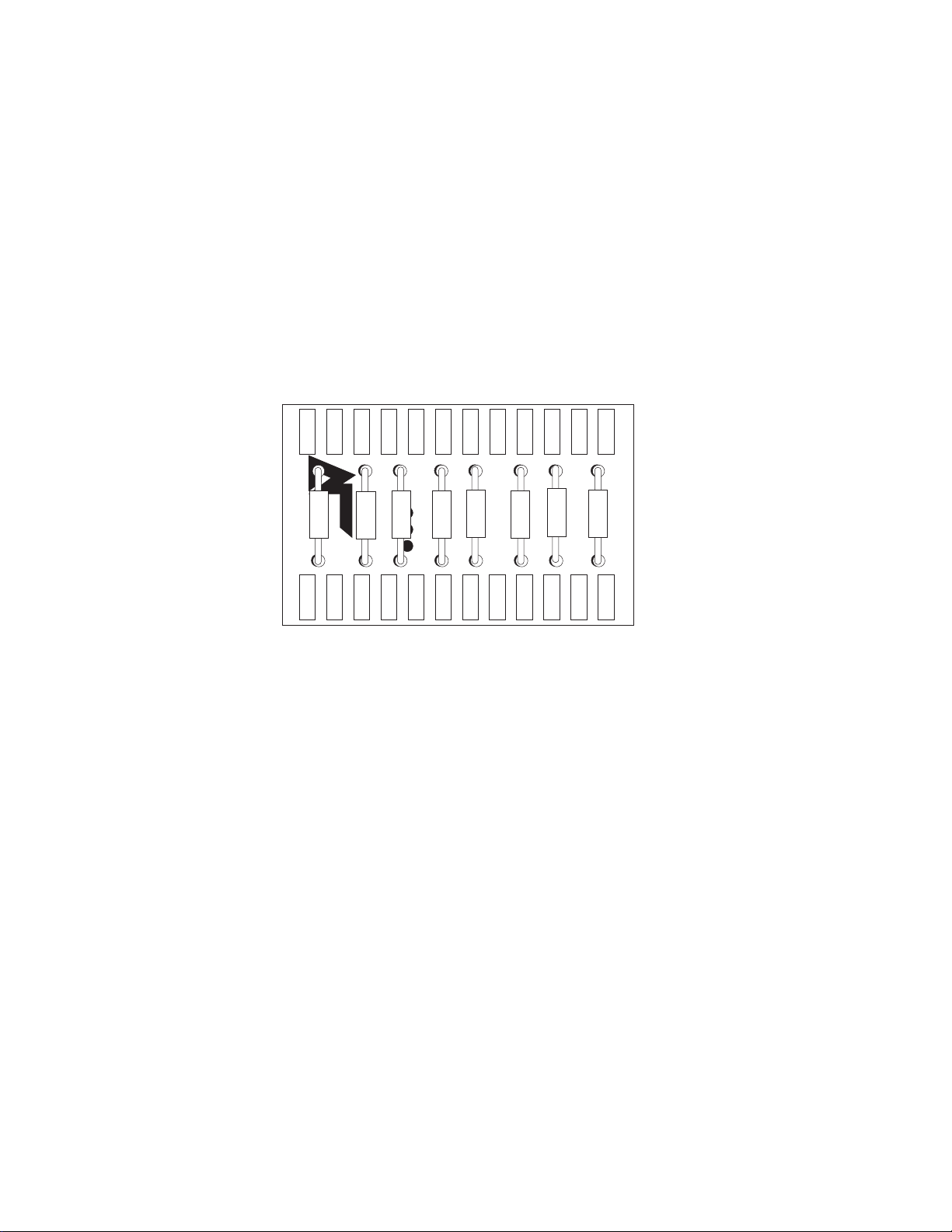
PC BOARD LAYOUT
– 7 –
Page 12

Page 13

P ARTS LIST
DESIGNATOR VALUE PART #
ALL RESISTORS IN OHMS
R1 56.2k, 1/4W, 1% RMP/4 5622-03
R2 1k, 1/4W, 5% RM/4-102C
R3 47k, 1/4W, 5% RM/4-473C
R4 47k, 1/4W, 5% RM/4-473C
R5 1k, 1/4W, 5% RM/4-102C
R6 280, 1/4W, 1% RM/4-2800C
R7 2.15k, 1/4W, 1% RM/4-2151C
R8 200 Trim Pot RVH-201
R9 2.26k, 1/4W, 1% RM/4-2261C
R10 28k, 1/4W, 1% RMP/4-2802
R11 300k, 1/4W, 5% RM/4-304C
R12 28k, 1/4W, 1% RM/4-2802C
R13 470k, 1/4W, 5% RM/4-474C
R14 100, 1/4W, 5% RM/4-101C
R15 3.3M, 1/4W, 5% RM/4-335C
R16 4.7k, 1/4W, 5% RM/4-472C
R17 10k, 1/4W, 5% RM/4-103C
R18 100k, 1/4W, 5% RM/4-104C
R19 604k, 1/4W, 1% RM/4-6043C
R20 45.3k, 1/4W, 1% RM/4-4532C
R21 2.2M, 1/4W, 5% RM/4-225C
R22 100k, 1/4W, 5% RM/4-104C
R23 100k, 1/4W, 5% RM/4-104C
R24 10k Pot, Dual RV-0818
R25 1k, 1/4W, 5% RM/4-102C
R26 2.2M, 1/4W, 5% RM/4-225C
R27 316, 1/4W, 1% RM/4-3160C
R28 316, 1/4W, 1% RM/4-3160C
R29 3.92k, 1/4W, 1% RM/4-3921C
R30 3.92k, 1/4W, 1% RM/4-3921C
R31 0, 1/4W, 1% RM/4-000C
R32 100, 1/4W, 5% RM/4-101C
R33 100, 1/4W, 5% RM/4-101C
R34 475, 1/4W, 1% RM/4-4750C
R35 220, 1/4W, 5% RM/4-221C
R36 1k, 1/4W, 5% RM/4-102C
R37 1k, 1/4W, 5% RM/4-102C
R38 3.3M, 1/4W, 5% RM/4-335C
R39 1k, 1/4W, 5% RM/4-102C
R40 1.5k, 1/4W, 5% RM/4-152C
R41 100, 1/4W, 5% RM/4-101C
R42 10k, 1/4W, 5% RM/4-103C
R43 15k, 1/4W, 5% RM/4-153C
R44 10k, 1/4W, 5% RM/4-103C
R45 15k, 1/4W, 5% RM/4-153C
R46 47k, 1/4W, 5% RM/4-473C
R47 10k, 1/4W, 5% RM/4-103C
R48 4.7k, 1/4W, 5% RM/4-472C
R49 6.8k, 1/4W, 5% RM/4-682C
R50 4.7k, 1/4W, 5% RM/4-472C
R51 4.7k, 1/4W, 5% RM/4-472C
R52 4.7k, 1/4W, 5% RM/4-472C
R53 2.2M, 1/4W, 5% RM/4-225C
R54 10k, 1/4W, 5% RM/4-103C
R55 100k, 1/4W, 5% RM/4-104C
R56 15k, 1/4W, 5% RM/4-153C
R57 10k, 1/4W, 5% RM/4-103C
R58 100k, 1/4W, 5% RM/4-104C
R59 10k, 1/4W, 5% RM/4-103C
R60 475, 1/4W, 1% RM/4-4750C
R61 100k, 1/4W, 5% RM/4-104C
R62 2.2M, 1/4W, 5% RM/4-225C
R63 10k, 1/4W, 5% RM/4-103C
R64 100k, 1/4W, 5% RM/4-104C
R65 475, 1/4W, 1% RM/4-4750C
R66 220, 1/4W, 5% RM/4-221C
R67 220, 1/4W, 5% RM/4-221C
R68 100, 1/4W, 5% RM/4-101C
R69 100, 1/4W, 5% RM/4-101C
DESIGNATOR VALUE PART #
R70 100, 1/4W, 5% RM/4-101C
R71 100, 1/4W, 5% RM/4-101C
R72 100, 1/4W, 5% RM/4-101C
R73 68, 1/4W RM/4-680C
R74 51, 1/4W, 5% RM/4-510C
R75 51, 1/4W, 5% RM/4-510C
R76 11.8k, 1/10W, 1% RM/10-1182B
R77 20k, 1/10W, 1% RM/10-2002B
R78 10M, 1/10W, 5% RM/10-106B
R79 11.8k, 1/10W, 1% RM/10-1182B
R80 20k, 1/10W, 1% RM/10-2002B
R81 10M, 1/10W, 5% RM/10-106B
R82 1k, 1/4W, 5% RM/4-102C
R83 10k, 1/4W, 5% RM/4-103C
R84 2k, 1/4W, 5% RM/4-202C
R85 1k, 1/4W, 5% RM/4-102C
R86 1k, 1/4W, 5% RM/4-102C
R87 4.7k, 1/4W, 5% RM/4-472C
R88 1.74k, 1/4W, 1% RM/4-1741C
R89 6.8k, 1/4W, 5% RM/4-682C
R90 10k, 1/4W, 5% RM/4-103C
R91 15k, 1/4W, 5% RM/4-153C
R92 4.7k, 1/4W, 5% RM/4-472C
R93 22k, 1/4W, 5% RM/4-223C
R94 100k, 1/4W, 5% RM/4-104C
R95 100k, 1/4W, 5% RM/4-104C
R96 22k, 1/4W, 5% RM/4-223C
R97 100k, 1/4W, 5% RM/4-104C
R98 4.7k, 1/4W, 5% RM/4-472C
R99 100k, 1/4W, 5% RM/4-104C
R123 2k, 1/4W, 5% RM/4-202C
R124 820, 1/4W, 5% RM/4-821C
R127 2k, 1/4W, 5% RM/4-202C
R128 100, 1/4W, 5% RM/4-101C
R129 100, 1/4W, 5% RM/4-101C
R130 2k, 1/4W, 5% RM/4-202C
R131 1k, 1/4W, 5% RM/4-102C
R132 1.5k, 1/4W, 5% RM/4-152C
R133 1k, 1/4W, 5% RM/4-102C
R134 47.5, 1/4W, 1% RM/4-0475C
R135 1k, 1/4W, 5% RM/4-102C
R136 200 Trim Pot RVH-201
R138 47.5, 1/4W, 1% RM/4-0475C
R139 475, 1/4W, 1% RM/4-4750C
R140 0, 1/4W, 1% RM/4-000C
R141 475, 1/4W, 1% RM/4-4750C
R159 475, 1/4W, 1% RM/4-4750C
R164 220, 1/4W, 5% RM/4-221C
C1 680pF, 100V CDS-681DBAA
C2 0.1µF, 50V CDS-104CCDB
C3 4700µF, 100V, Electrolytic CERS-478E
C4 0.1µF, 50V CDS-104CCDB
C5 4700µF, 100V, Electrolytic CERS-478E
C6 270pF, 50V CDS-271CAAA
C7 270pF, 50V CDS-271CAAA
C8 27pF, 100V CDS-270DAAA
C9 0.1µF, 50V CDS-104CCDB
C10 4700µF, 100V, Electrolytic CERS-478E
C11 4700µF, 100V, Electrolytic CERS-478E
C12 4700µF, 100V, Electrolytic CERS-478E
C13 470µF, 50V, Electrolytic CER-477C-024
C14 470µF, 50V, Electrolytic CER-477C-024
C15 0.1µF, 50V CDS-104CCDB
C16 0.1µF, 50V CDS-104CCDB
C17 0.1µF, 50V CDS-104CCDB
C18 0.1µF, 50V CDS-104CCDB
C19 0.1µF, 50V CDS-104CCDB
C20 0.1µF, 50V CDS-104CCDB
– 10 –
Page 14

DESIGNATOR VALUE PART #
DESIGNATOR VALUE PART #
C21 10µF, 16V, Electrolytic CER-106SM
C22 10µF, 16V, Electrolytic CER-106SM
C23 0.47µF, 50V CYV-474-024
C24 0.47µF, 50V CYV-474-024
C25 0.1µF, 50V CDS-104CCDB
C26 0.1µF, 50V CDS-104CCDB
C27 4700µF, 100V, Electrolytic CERS-478E
C28 47µF, 16V, Electrolytic CER-476-024
C29 10µF, 50V, Electrolytic CER-106C-024
C30 0.1µF, 50V CDS-104CCDB
C31 0.1µF, 50V CDS-104CCDB
C32 27pF, 50V CDS-270CAAA
C33 0.1µF, 50V CDS-104CCDB
C34 27pF, 50V CDS-270CAAA
C35 22pF, 500V, Mica CM-220-024
C36 47pF, 500V, Mica CM-470-024
C37 0.1µF, 50V CDS-104CCDB
C38 0.1µF, 50V CDS-104CCDB
C39 1.0µF, 50V, Electrolytic CER-105CSM
C40 0.1µF, 50V CDS-104CCDB
C42 0.01µF, 1kV, Disk CD-103/20-024
C43 0.1µF, 50V CDS-104CCDB
C44 0.1µF, 50V CDS-104CCDB
C45 100pF, 50V CDS-101CAAA
C46 22pF, 500V, Mica CM-220-024
C47 0.047µF, 50V CDS-473CBBA
C48 0.1µF, 50V CDS-104CCDB
C49 0.1µF, 50V CDS-104CCDB
C50 27pF, 100V CDS-270DAAA
C112 100µF, 25V, Electrolytic CER-107A-024
C113 100µF, 25V, Electrolytic CER-107A-024
C114 100pF, 50V CDS-101CAAA
C115 100pF, 50V CDS-101CAAA
C116 0.047µF, 50V CDS-473CBBA
C119 0.1µF, 100V, Mylar CY-104-024
C120 0.1µF, 100V, Mylar CY-104-024
Q1 MMBT5088L SS-0114
Q2 LM-317 + Regulator SS-239-046
Q3 LM-337 – Regulator SS-240-046
Q4 MMBT3904L SS-0792
Q5 MMBT5087L SS-0115
Q6 MMBT5088L SS-0114
Q7 MMBT5088L SS-0114
Q8 MMBT3904L SS-0792
Q9 MPS-A56 SS-101A
Q10 MPS-A56 SS-101A
Q11 MPS-A06 SS-102A
Q12 MPS-A06 SS-102A
Q17 MMBT5088L SS-0114
Q18 MMBT5087L SS-0115
Q19 2N-6488 SS-112C-046
Q20 MMBT3904L SS-0792
Q30 N Channel MOSFET SS-0961-069
Q31 N Channel MOSFET SS-0961-069
Q32 N Channel MOSFET SS-0961-069
Q33 N Channel MOSFET SS-0961-069
Q40 P Channel MOSFET SS-0962-069
Q41 P Channel MOSFET SS-0962-069
Q42 P Channel MOSFET SS-0962-069
Q43 P Channel MOSFET SS-0962-069
Q103 MMBT5088L SS-0114
Q104 MMBT5087L SS-0115
Q105 MMBT5087L SS-0115
CR5 MMBD914L Diode SS-803SM
CR6 MMBD914L Diode SS-803SM
CR7 MMBD914L Diode SS-803SM
CR8 MMBD914L Diode SS-803SM
CR9 MMBZ5240BL 10V Zener Diode SS-1052
CR10 Bridge Rectifier 1.5A SS-0800
CR11 BAV99L Dual Diode SS-260SM
CR12 BAV99L Dual Diode SS-260SM
CR13 MMBD914L Diode SS-803SM
CR14 BAV99L Dual Diode SS-260SM
CR15 BAV99L Dual Diode SS-260SM
CR16 BAV99L Dual Diode SS-260SM
CR18 MMBZ5240BL 10V Zener Diode SS-1052
CR19 BAV99L Dual Diode SS-260SM
U1 TL072CD Opamp SS-143SM
U2 TL072CD Opamp SS-143S
U3 LM-393 Dual Comparator SS-207SM
U4 LM339 Quad Comparator SS-730SM
U5 LM339 Quad Comparator SS-730SM
U6 XCard Connector CC-0233
U7 TL072CD Opamp SS-143SM
U8 XCard Connector CC-0233
U9 LM-393 Dual Comparator SS-207SM
J1 Input Jack, Combo CC-0588
Dual Binding Post CC-0867
Binding Post Back Plate HW-0908
Binding Post Mounting Nut HW-0905
J301 Line Cord Socket CC-0918
Line Cord 14/3 FA-0209
SL1 Surge Limiter FA-1000-B
Fuse Holder, Cap FS-0828
Fuse Holder, Body FS-0829
Fuse Holder Washer FS-0827
Fan, 80x25mm, 24VDC FAN-0990
Level Control Cover HP-0878
Level Control Knob KN-0838
Adhesive Feet HWH-169
SW1 DPDT Slide Switch SW-0280
SW2 DPDT Slide Switch SW-0280
SW3 DPDT Slide Switch SW-0280
SW4 Power Switch SWH-152B
F1 Line Fuse, 15A Slo Blo FS-015SB
TS1 Thermistor 10k, NTC SS-0426-066
Tranformer TT-0958-B
Rack Handle HW-1017-A
Rack Ears SM-1016-C
BR1 Bridge Rectifier SSH-609
CR1 LED Red SS-741
CR2 LED Red SS-741
CR3 LED Red SS-741
CR4 LED Green SS-740
– 11 –
Page 15

P7000 FUNCTIONAL BLOCK DIAGRAM
Positive Input
Buffer
U1A
Balanced
Signal
Negative Input
Buffer
U1B
XCard
Crossover
U7A
Crossover
U7B
XCard
Level
Control
R24
Input Buffer
U2a
CMRR
Adjust
R8
DC Offset
Integrator
U2B, C22, C21,
R11
Soft Start
Switch Delay
Q1, C29, R13
Current Mirror
Q104, Q105
Differential Amp
Q6, Q7
Current
Source
Q103
DIABLO
R73, CR16
Q17, Q18
Feedback
Network
Driver Cascode
Q9, Q10
Driver Cascode
Q11, Q12
Bias
Adjust
R136
Local
Feedback
Output
Q30, Q31,
Q32, Q33
Output
Q40, Q41,
Q42, Q43
Output
B+
+94V
B–
–94V
– 12 –
Page 16

CIRCUIT OPERATION
trans•nova Implementation
The transistor Q1 is configured to operate as a switch which controls the current source, Q103, of the input differential
amp, Q6 and Q7. When Q1 is off the emitter voltage is low turning off Q103. Timing of the Soft Start function is controlled
by the charging time of C29 through R13. The THERMAL Protection circuit uses Q1 to shut down the channel when
excessive heat is detected. The OVERLOAD protection switch Q5 and Q4 turn off Q3 directly when a short is detected
on the output.
U1A and U1B are buffer amps configured as unity gain, non-inverting voltage followers which feed the crossover filters
U7A and U7B. The feedback components which control the crossover functions are contained on the XCard plug-in
module. The output of the filters is fed to the attenuator network controlled by R24. The output of U2A and U7B is
connected to the input of the differential amp. U2B is configured as a DC servo integrator to null the input offset currents.
The output of the differential amp is fed to the driver stage by Q17 and Q18 which perform the DIABLO
transconductance steering function. The cascode pairs Q9, Q10 and Q11, Q12 supply the signal voltage and current
needed to drive the output stage Q30, Q31, Q32, Q33 and Q40, Q41, Q42, Q43. Class AB bias current is controlled
by R136. Loop feedback is supplied by the network R1 and C1, and global feedback by R10, C8 and C41.
Adjusting Bias:
The bias control establishes the quiescent Class AB output current of the amplifier. The bias should not need
readjustment from the factory setting; however, if the amplifier is repaired and output devices have been changed, or
if the two channels of the amplifier do not run at the same temperature, recalibrating the bias is necessary. Disconnect
the power to the amplifier before removing the cover. To adjust the bias, disconnect the input and speakers and remove
the jumper JW7. Connect an amp meter across the exposed pins. The correct polarity is marked adjacent to the jumper.
Adjust R136 to get a current reading of 400mA.
Calibrating Common Mode Rejection:
The input common mode null is adjusted by the trim pot R8. The CMRR should be greater than 75dB below rated output.
If the CMRR requires adjustment, feed the amplifier input with a common mode signal and adjust R8. Disconnect the
power to the amplifier before removing the cover. Use a sinewave generator set to 1 volt output at 1kHz. Connect the
generator signal output to the tip and ring of a 1/4" plug and ground to the sleeve. Plug this into the amplifier input.
Connect an AC voltmeter to the amplifier output binding posts. Adjust R8 to give the lowest voltage output from the
amplifier. For a temporary adjustment when a signal generator and voltmeter are not available, use an FM tuner and
tune it to an unused station as your signal source, and connect the output to the amplifier as described above. Connect
the amplifier output to a small full range speaker. Turn the amplifier level controls full down and turn the amplifier on.
Turn up the level control until you hear a signal through the speaker. Alternate between adjusting R8 for the lowest output
signal and increasing the input control until you have the level control full. There should be a very low output from the
amplifier if any is detected at all.
– 13 –
Page 17

Fan Speed Regulation
Driver
U9A
Temp
TS1, R25
Trip Switch
U9B
Fan Drive
Amp
Q20, Q19
Cooling air for each channel is provided by a DC fan. The fan is configured to track the heatsink temperature, and
increases in speed as the amplifier runs hotter. The heatsink temperature, Temp, is determined by the voltage divider
TS1 and R25. When the amplifier is turned on the fan will stay off until the Temp voltage exceeds the reference voltage
on pin 6 of the Trip Switch U9B and drives the output high to turn on the Fan Drive Amplifier, Q20 and Q19. The Driver
U9A is configured as a linear amplifier and controls the output of the Fan Drive Amp to vary the fan speed.
Output Short Protection
Drive
Signal
Clip Detector
U3A
Clip Detector
U4A
Comparator
U3B
Short Latch
U4C, CR14
Shut Down
Switch
Q5, Q4
Comparator
U4A
Output
Signal
Short
Indicator
CR1
The Short detector monitors the Drive Signal and Output Signal levels and shuts down that channel when a shorted
output condition is detected. Recovering from the Short protection requires turning the amplifier off to reset it.
The Clip Detectors U3A and U4B monitor the Drive Signal and change state when the drive signal level is sufficient to
clip the output stage. The output of U3A goes high when the drive signal exceeds the clip threshold, and is connected
to the input of U3B. If the output signal voltage is not sufficiently positive during a clip event the output of U3B goes
low. The output of U4B goes low when the drive signal exceeds the clip threshold, and is connected to the input of U4A.
If the output signal voltage is not sufficiently negative during a clip event the output of U4A goes low.
This condition, indicating high drive voltage and low output voltage, can occur only when the output is grounded. If
the output of comparator stage U3B or U4A is low for the time sufficient for C26 to charge, then U4C latches low
activating the Shut Down Switch Q5 and Q4, and lighting the indicator CR1. The output of U4C is held low by CR14
and will reset only after the power is turned off.
– 14 –
Page 18

Thermal Protection
Soft Start Switch
Q1
Temp
TS1, R25
Comparator
U5B
THERMAL Indicator
CR2
The Thermal protection is activated, and shuts down audio operation, when the amplifier heatsink reaches an
excessively high temperature. The voltage divider R22 and R23 establishes the reference voltage on pin 5 of U5B. The
control voltage, Temp, on pin 4 is established by the voltage divider TS1 and R25. TS1 is a NTC (Negative Temperature
Coefficient) thermistor, mounted on the heatsink. As TS1 warms and the resistance falls, the voltage on pin 4 rises. When
the voltage on pin 4 exceeds the voltage on pin 5, the output on pin 2 goes low, shutting down the Soft Start switch Q1
and lighting the THERMAL indicator.
Clipping Indicator
Drive
Signal
Clipping
Detector
U5A
LED Driver
U5C
CLIP Indicator
CR3
The CLIP indicator is driven by the buffer U5C which is controlled by the comparator U5A. The voltage divider R56
and R57 established the reference voltage for the clipping detector at pin 7 of U5A. The reference voltage scales the
output of U5A to indicate when the Drive Signal, at pin 6, demands in excess of the available voltage or current of the
output stage. The output of U5A is stretched by R55 and C30 to prevent the CLIP indicator CR3 from flickering. Hysteresis
is applied to the LED driver U5C by R53 to stabilize the output during input transitions.
Signal Present Indicator
Amplifier
Output
Signal
Detector
U5D
LED Driver
Q8
SIGNAL
Indicator
CR4
The SIGNAL indicator is controlled by the comparator U5D and the transistor Q8. The amplifier output is connected
to the input pin 9. The voltage divider R58 and R59 scales the output voltage to change the comparator output state at
an equivalent input voltage of 30mV. The output at pin 14 controls the transistor Q8 to shunt across and turn off the LED
CR4.
– 15 –
Page 19

AMPLIFIER MODULE REPLACEMENT
The amplifier modules have been designed to eliminate the need for a special workplace if a field exchange becomes
necessary. All wire connections are made with quick connect terminals so soldering is not necessary. The following
tools are needed to disassemble the amplifier:
Allen wrench, 9/64
Phillips screwdriver, #1 tip
Thin nose pliers
Small cutters
Remove the four Phillips head screws, located on the rear panel, which secure the input jacks. Remove the six 9/64
Allen screws that hold the cover. These are located along the top edge, two on each side and two on the rear. Lift the
cover from the rear and remove it. Remove the level control knob. The wire harnesses have been bundled for neatness.
Cut the ties to free the bundles.
Disconnect the red and black output wires from the binding posts and the fan and power wires from the amplifier drive
card. Disconnect the transformer secondary wires from the bridge rectifier and PC board. Unplug the gray mono cables.
The heatsink is attached to the chassis by three screws, two outside and one inside. Remove the two 9/64 Allen screws
on the bottom edge of the side of the amplifier. Remove the Phillips screw located behind the level control, which is
accessible through the hole in the PC board. The module can now be lifted from the chassis.
Prepare a new Channel 1 module for installation by setting the input mode switches to the default position according
to the markings adjacent to the switches. Prepare a Channel 2 module by duplicating the switch settings of the module
which was removed.
Install the new module and check the position and alignment of the indicator LEDs. Replace the level control knob and
check the alignment while securing the module.
Plug in the gray mono cables. The headers are marked with the proper position for Channel 1 and Channel 2. The plugs
are oriented so the cable will fit properly in one direction only.
Reconnect the remaining wires according to the following chart.
Wire Color Function Terminal
Red Audio Output Red Binding Post
Black Output Ground Black Binding Post
Orange (two) High Voltage AC Bridge Rectifier AC
White High Voltage Center Tap CTI
Red High Voltage DC Positive + Red
Blue High Voltage DC Negative – BLUE
White/Blue Low Voltage Center Tap CT2
Blue (two) Low Voltage AC LV1, LV2
– 16 –
Page 20
BUILDING CUSTOM XCARDS
The XCard crossover control modules used in the P7000 are a versatile and inexpensive method for configuring the
amplifier for a wide range of system applications. The XCard eliminates the need for an external crossover or expensive
plug-in accessories for multiple amp applications. By having the crossover built into the amplifier input circuit and with
the XCard containing all the components controlling the operating frequency, it is very simple to customize to meet
system specific requirements. Each amplifier, as supplied, has two 100Hz Butterworth aligned XCards each of which
contains two resistors and two capacitors to control the crossover frequency. The XCard will operate as either a highpass or low-pass filter, depending upon its orientation. The following tools are needed to build the XCards:
Soldering Iron (appropriate for PC board work)
Solder (suitable for electronics)
Desoldering Braid
Our tests have shown that for operating frequencies at 100Hz and lower using 0.047µF capacitors results in more linear
crossover control. For frequencies above 100Hz use 0.022µF, the voltage rating should be a minimum of 10V.
Use 1/8 or 1/4 watt 1% metal film resistors. Solder the components to the card according to the following diagram.
Crossover Card
C1
R1
High Pass
C2
R2
Low Pass
Full Range
C1
R1
FULL
C2
R2
– 17 –
Page 21

RESISTOR CHART
The following charts list the resistor values to use for common crossover frequencies.
Butterworth Alignment Q = .707
1% resistors used with 0.047µF capacitors
Frequency R1 R2
20Hz 169kΩ 169kΩ
25Hz 133kΩ 133kΩ
30Hz 110kΩ 110kΩ
35Hz 95.3kΩ 95.3Ω
40Hz 84.5kΩ 84.5kΩ
45Hz 75kΩ 75kΩ
50Hz 68.1kΩ 68.1kΩ
55Hz 61.9kΩ 61.9kΩ
60Hz 56.2kΩ 56.2kΩ
65Hz 52.3kΩ 52.3kΩ
70Hz 48.7kΩ 48.7kΩ
75Hz 45.3kΩ 45.3kΩ
80Hz 42.2kΩ 42.2kΩ
84Hz 40.2kΩ 40.2kΩ
90Hz 37.4kΩ 37.4kΩ
200Hz 16.9kΩ 16.9kΩ
300Hz 11.3kΩ 11.3kΩ
400Hz 8.45kΩ 8.45kΩ
500Hz 6.65kΩ 6.65kΩ
600Hz 5.62kΩ 5.62kΩ
700Hz 4.75kΩ 4.75kΩ
800Hz 4.22kΩ 4.22kΩ
900Hz 3.74kΩ 3.74kΩ
1kHz 3.40kΩ 3.40kΩ
1.2kHz 2.8kΩ 2.8kΩ
2kHz 1.69kΩ 1.69kΩ
3kHz 1.10kΩ 1.10kΩ
4kHz 845Ω 845Ω
5kHz 665Ω 665Ω
6kHz 562Ω 562Ω
7kHz 487Ω 487Ω
8kHz 422Ω 422Ω
Butterworth Alignment Q = .707
1% resistors used with 0.022µF capacitors
Frequency R1 R2
20Hz 357kΩ 357kΩ
25Hz 287kΩ 287kΩ
30Hz 237kΩ 237kΩ
35Hz 205kΩ 205kΩ
40Hz 178kΩ 178kΩ
45Hz 162kΩ 162kΩ
50Hz 143kΩ 143kΩ
55Hz 130kΩ 130kΩ
60Hz 121kΩ 121kΩ
65Hz 110kΩ 110kΩ
70Hz 102kΩ 102kΩ
75Hz 95.3kΩ 95.3kΩ
80Hz 90.9kΩ 90.9kΩ
85Hz 84.5kΩ 84.5kΩ
90Hz 80.6kΩ 80.6kΩ
200Hz 35.7kΩ 35.7kΩ
300Hz 23.7kΩ 23.7kΩ
400Hz 17.8kΩ 17.8kΩ
500Hz 14.3kΩ 14.3kΩ
600Hz 12.1kΩ 12.1kΩ
700Hz 10.2kΩ 10.2kΩ
800Hz 9.9kΩ 9.9kΩ
900Hz 8.6kΩ 8.6kΩ
1kHz 7.15kΩ 7.15kΩ
1.2kHz 6.04kΩ 6.04kΩ
2.0kHz 3.57kΩ 3.57kΩ
3.0kHz 2.37kΩ 2.37kΩ
4.0kHz 1.76kΩ 1.76kΩ
5.0kHz 1.43kΩ 1.43kΩ
6.0kHz 1.21kΩ 1.21kΩ
7.0kHz 1.02kΩ 1.02kΩ
8.0kHz 909Ω 909Ω
To calculate the resistor value for a frequency not on the chart use the following:
3386
f
o
= R (in kΩ) for .047µf cap
The actual formula is: R =
Where: R = Ω
7234
f
o
= R (in kΩ) for .022µf cap
fo = desired crossover frequency
c = capacitor in farads
ex: .047 x 10-6 for .047mf cap
– 18 –
2πf
1
c
o
Page 22

SERVICE POLICY AND LIMITED WARRANTY
If you encounter any difficulty or have any question concerning your P7000 Amplifier, please call our Technical Support
Department weekdays, 8:00 a.m. to 3:30 p.m., Mountain Standard Time, at 800-743-3526.
Should you have any doubts as to whether the amplifier is malfunctioning and requires service, please call us before
sending it in for repair. All units being returned (regardless of warranty status) must receive a Return Authorization (RA)
number. In addition, we can offer troubleshooting assistance that may simplify or even eliminate the need for factory
service.
The Hafler P7000 Amplifier is warranted to the original owner (non-transferrable) for seven years from the date of
purchase, including parts, labor, and return shipping costs within the Continental United States, Alaska, and Hawaii.
This warranty applies only to products sold in the United States of America.
For warranties outside the U.S.A., please contact your local agent.
It is the owner’s responsibility to pay shipping (preferably United Parcel Service, UPS) to the factory: collect shipments
will not be accepted. Units under warranty should be accompanied by a copy of the dated Bill Of Sale. Use the original
carton and all packing material, with the RA number clearly marked on the outside of the package. Be sure to include
a return address, the RA number, a daytime telephone number, and a brief description of the difficulty, including whether
it occurs continuously or intermittently.
This warranty gives you specific legal rights. You may also have other rights which may vary from state to state.
– 19 –
Page 23

HAFLER PROFESSIONAL
A DIVISION OF
ROCKFORD CORPORATION
546 SOUTH ROCKFORD DRIVE
TEMPE, ARIZONA 85281 U.S.A.
IN U.S.A. (602) 967-3565
IN CANADA, (604) 942-1001
IN EUROPE, FAX (49) 4207-801250
IN JAPAN, FAX (81) 559-79-01265
MAN-0963-B
9/95
Page 24

 Loading...