


GSI GS88236B-80I, GS88236B-80, GS88236B-66I, GS88236B-66, GS88236B-11I Datasheet
...Preliminary
GS88218/36B-11/11.5/100/80/66
119-Bump BGA |
512K x 18, 256K x 36 ByteSafe™ |
100 MHz–66 MHz |
Commercial Temp |
8Mb S/DCD Sync Burst SRAMs |
3.3 V VDD |
Industrial Temp |
3.3 V and 2.5 V I/O |
|
|
|
|
|
|
|
Features
•FT pin for user-configurable flow through or pipeline operation
•Single/Dual Cycle Deselect Selectable
•IEEE 1149.1 JTAG Compatible Boundary Scan
•On-chip write parity checking; even or odd selectable
•ZQ mode pin for user-selectable high/low output drive strength
•x16/x32 mode with on-chip parity encoding and error detection
•3.3 V +10%/–5% core power supply
•2.5 V or 3.3 V I/O supply
•LBO pin for Linear or Interleaved Burst mode
•Internal input resistors on mode pins allow floating mode pins
•Default to SCD x18/x36 Interleaved Pipelined mode
•Byte Write (BW) and/or Global Write (GW) operation
•Common data inputs and data outputs
•Clock Control, registered, address, data, and control
•Internal self-timed write cycle
•Automatic power-down for portable applications
•119-bump BGA package
|
|
-11 |
-11.5 |
-100 |
-80 |
-66 |
|
|
|
|
|
|
|
Pipeline |
tCycle |
10 ns |
10 ns |
10 ns |
12.5 ns |
15 ns |
3-1-1-1 |
tKQ |
4.0 ns |
4.0 ns |
4.0 ns |
4.5 ns |
5 ns |
|
IDD |
225 mA |
225 mA |
225 mA |
200 mA |
185 mA |
Flow |
tKQ |
11 ns |
11.5 ns |
12 ns |
14 ns |
18 ns |
Through |
tCycle |
15 ns |
15 ns |
15 ns |
15 ns |
20 ns |
2-1-1-1 |
IDD |
180 mA |
180 mA |
180 mA |
175 mA |
165 mA |
Functional Description
Applications
The GS88218/36B is a 9,437,184-bit high performance synchronous SRAM with a 2-bit burst address counter. Although of a type originally developed for Level 2 Cache applications supporting high performance CPUs, the device now finds application in synchronous SRAM applications, ranging from DSP main store to networking chip set support.
Controls
Addresses, data I/Os, chip enables (E1 and E2), address burst control inputs (ADSP, ADSC, ADV), and write control inputs (Bx, BW, GW) are synchronous and are controlled by a positive-edge-triggered clock input (CK). Output enable (G) and power down control (ZZ) are asynchronous inputs. Burst cycles can be initiated with either ADSP or ADSC inputs. In Burst mode, subsequent burst addresses are generated internally and are controlled by ADV. The burst address counter may be configured to count in either linear or interleave order with the Linear Burst Order (LBO) input. The Burst function need not be used. New addresses can be loaded
on every cycle with no degradation of chip performance.
Flow Through/Pipeline Reads
The function of the Data Output Register can be controlled by
the user via the FT mode bump (Bump 5R). Holding the FT mode pin low places the RAM in Flow Through mode, causing
output data to bypass the Data Output Register. Holding FT high places the RAM in Pipeline mode, activating the rising- edge-triggered Data Output Register.
SCD and DCD Pipelined Reads
The GS88218/36B is a SCD (Single Cycle Deselect) and DCD (Dual Cycle Deselect) pipelined synchronous SRAM. DCD SRAMs pipeline disable commands to the same degree as read commands. SCD SRAMs pipeline deselect commands one stage less than read commands. SCD RAMs begin turning off their outputs immediately after the deselect command has been captured in the input registers. DCD RAMs hold the deselect command for one full cycle and then begin turning off their outputs just after the second rising edge of clock. The user may configure this SRAM for either mode of operation using the SCD mode input on Bump 4L.
Byte Write and Global Write
Byte write operation is performed by using Byte Write enable (BW) input combined with one or more individual byte write signals (Bx). In addition, Global Write (GW) is available for writing all bytes at one time, regardless of the Byte Write control inputs.
ByteSafe™ Parity Functions
The GS88218/36B features ByteSafe data security functions. See “ByteSafe™ Parity Functions” on page 8 for further information.
FLXDrive™
The ZQ pin allows selection between high drive strength (ZQ low) for multi-drop bus applications and normal drive strength (ZQ floating or high) point-to-point applications. See the
Output Driver Characteristics chart on page 38 for details.
Sleep Mode
Low power (Sleep mode) is attained through the assertion (High) of the ZZ signal, or by stopping the clock (CK). Memory data is retained during Sleep mode.
Core and Interface Voltages
The GS88218/36B operates on a 3.3 V power supply and all inputs/outputs are 3.3 V- and 2.5 V-compatible. Separate output power (VDDQ) pins are used to decouple output noise from the internal circuit.
Rev: 1.15 5/2001 |
1/39 |
© 2000, Giga Semiconductor, Inc. |
Specifications cited are subject to change without notice. For latest documentation see http://www.gsitechnology.com.

Preliminary
GS88218/36B-11/11.5/100/80/66
GS88236 Pad Out
119-Bump BGA—Top View
|
1 |
2 |
3 |
|
4 |
|
|
|
|
|
5 |
|
|
6 |
7 |
|
||||||||||||
A |
|
|
|
|
|
|
|
|
|
|
|
|
|
|
|
|
|
|
|
|
|
|
|
|
|
|
|
|
|
|
|
|
|
|
|
|
|
|
|
|
|
|
|
|
|
|
|
|
|
|
|
|
|
|
|
|
|
VDDQ |
A6 |
|
|
A7 |
|
ADSP |
|
A8 |
A9 |
VDDQ |
||||||||||||||||||
B |
|
|
|
|
|
|
|
|
|
|
|
|
|
|
|
|
|
|
|
|
|
|
|
|
|
|
|
|
NC |
E2 |
|
|
A4 |
ADSC |
A15 |
A17 |
NC |
||||||||||||||||||||
C |
NC |
A5 |
|
|
A3 |
|
|
VDD |
A14 |
A16 |
NC |
|||||||||||||||||
D |
DQC4 |
DQC9 |
|
VSS |
|
|
|
ZQ |
VSS |
DQB9 |
DQB4 |
|||||||||||||||||
E |
|
|
|
|
|
|
|
|
|
|
|
|
|
|
|
|
|
|
|
|
|
|
|
|
|
|
|
|
DQC3 |
DQC8 |
|
VSS |
|
|
|
|
E1 |
VSS |
DQB8 |
DQB3 |
|||||||||||||||||
F |
|
|
|
|
|
|
|
|
|
|
|
|
|
|
|
|
|
|
|
|
|
|
|
|
|
|
||
VDDQ |
DQC7 |
|
VSS |
|
|
|
|
|
G |
VSS |
DQB7 |
VDDQ |
||||||||||||||||
G |
|
|
|
|
|
|
|
|
|
|
|
|
|
|
|
|
|
|
|
|
|
|
|
|||||
DQC2 |
DQC6 |
|
|
BC |
|
ADV |
|
BB |
DQB6 |
DQB2 |
||||||||||||||||||
H |
|
|
|
|
|
|
|
|
|
|
|
|
|
|
|
|
|
|
|
|||||||||
DQC1 |
DQC5 |
|
VSS |
|
|
|
GW |
VSS |
DQB5 |
DQB1 |
||||||||||||||||||
J |
|
|
|
|
|
|
|
|
|
|
|
|
|
|
|
|
|
|
||||||||||
VDDQ |
VDD |
|
DP |
|
|
VDD |
|
QE |
VDD |
VDDQ |
||||||||||||||||||
K |
DQD1 |
DQD5 |
|
VSS |
|
|
|
CK |
VSS |
DQA5 |
DQA1 |
|||||||||||||||||
L |
|
|
|
|
|
|
|
|
|
|
|
|
|
|
|
|
|
|
|
|||||||||
DQD2 |
DQD6 |
|
|
BD |
|
SCD |
|
BA |
DQA6 |
DQA2 |
||||||||||||||||||
M |
|
|
|
|
|
|
|
|
|
|
|
|
|
|
|
|
|
|||||||||||
VDDQ |
DQD78 |
|
VSS |
|
|
|
BW |
VSS |
DQA7 |
VDDQ |
||||||||||||||||||
N |
DQD3 |
DQD8 |
|
VSS |
|
|
|
|
A1 |
VSS |
DQA8 |
DQA3 |
||||||||||||||||
P |
DQD4 |
DQD9 |
|
VSS |
|
|
|
|
A0 |
VSS |
DQA9 |
DQA4 |
||||||||||||||||
R |
|
|
|
|
|
|
|
|
|
|
|
|
|
|
|
|||||||||||||
NC |
A2 |
LBO |
|
|
VDD |
|
FT |
A13 |
PE |
|||||||||||||||||||
T |
NC |
NC |
|
A10 |
|
|
|
A11 |
A12 |
NC |
|
ZZ |
||||||||||||||||
U |
VDDQQ |
TMS |
|
TDI |
|
|
TCK |
TDO |
NC |
VDDQ |
||||||||||||||||||
Rev: 1.15 5/2001 |
2/39 |
© 2000, Giga Semiconductor, Inc. |
Specifications cited are subject to change without notice. For latest documentation see http://www.gsitechnology.com.

Preliminary
GS88218/36B-11/11.5/100/80/66
GS88218 Pad Out
119-Bump BGA—Top View
|
1 |
2 |
3 |
|
4 |
|
|
|
|
|
5 |
|
|
6 |
7 |
|
||||||||||||
A |
|
|
|
|
|
|
|
|
|
|
|
|
|
|
|
|
|
|
|
|
|
|
|
|
|
|
|
|
|
|
|
|
|
|
|
|
|
|
|
|
|
|
|
|
|
|
|
|
|
|
|
|
|
|
|
|
|
VDDQ |
A6 |
|
|
A7 |
|
ADSP |
|
A8 |
A9 |
VDDQ |
||||||||||||||||||
B |
|
|
|
|
|
|
|
|
|
|
|
|
|
|
|
|
|
|
|
|
|
|
|
|
|
|
|
|
NC |
E2 |
|
|
A4 |
ADSC |
A15 |
A17 |
NC |
||||||||||||||||||||
C |
NC |
A5 |
|
|
A3 |
|
|
VDD |
A14 |
A16 |
NC |
|||||||||||||||||
D |
DQB1 |
NC |
|
VSS |
|
|
|
ZQ |
VSS |
DQA9 |
NC |
|||||||||||||||||
E |
|
|
|
|
|
|
|
|
|
|
|
|
|
|
|
|
|
|
|
|
|
|
|
|
|
|
|
|
NC |
DQB2 |
|
VSS |
|
|
|
|
E1 |
VSS |
NC |
DQA8 |
|||||||||||||||||
F |
|
|
|
|
|
|
|
|
|
|
|
|
|
|
|
|
|
|
|
|
|
|
|
|
|
|
||
VDDQ |
NC |
|
VSS |
|
|
|
|
|
G |
VSS |
DQA7 |
VDDQ |
||||||||||||||||
G |
|
|
|
|
|
|
|
|
|
|
|
|
|
|
|
|
|
|
|
|
|
|
|
|||||
NC |
DQB3 |
|
|
BB |
|
ADV |
|
NC |
NC |
DQA6 |
||||||||||||||||||
H |
|
|
|
|
|
|
|
|
|
|
|
|
|
|
|
|
|
|
|
|
||||||||
DQB4 |
NC |
|
VSS |
|
|
|
GW |
VSS |
DQA5 |
NC |
||||||||||||||||||
J |
|
|
|
|
|
|
|
|
|
|
|
|
|
|
|
|
|
|
|
|||||||||
VDDQ |
VDD |
|
DP |
|
|
VDD |
|
QE |
VDD |
VDDQ |
||||||||||||||||||
K |
NC |
DQB5 |
|
VSS |
|
|
|
CK |
VSS |
NC |
DQA4 |
|||||||||||||||||
L |
|
|
|
|
|
|
|
|
|
|
|
|
|
|
|
|
|
|||||||||||
DQB6 |
NC |
|
NC |
|
SCD |
|
BA |
DQA3 |
NC |
|||||||||||||||||||
M |
|
|
|
|
|
|
|
|
|
|
|
|
|
|
|
|
|
|||||||||||
VDDQ |
DQB7 |
|
VSS |
|
|
|
BW |
VSS |
NC |
VDDQ |
||||||||||||||||||
N |
DQB8 |
NC |
|
VSS |
|
|
|
|
A1 |
VSS |
DQA2 |
NC |
||||||||||||||||
P |
NC |
DQB9 |
|
VSS |
|
|
|
|
A0 |
VSS |
NC |
DQA1 |
||||||||||||||||
R |
|
|
|
|
|
|
|
|
|
|
|
|
|
|
|
|||||||||||||
NC |
A2 |
LBO |
|
|
VDD |
|
FT |
A13 |
PE |
|||||||||||||||||||
T |
NC |
A10 |
|
A11 |
|
|
|
NC |
A12 |
A18 |
|
ZZ |
||||||||||||||||
U |
VDDQ |
TMS |
|
TDI |
|
|
TCK |
TDO |
NC |
VDDQ |
||||||||||||||||||
Rev: 1.15 5/2001 |
3/39 |
© 2000, Giga Semiconductor, Inc. |
Specifications cited are subject to change without notice. For latest documentation see http://www.gsitechnology.com.

|
|
|
|
|
|
|
|
Preliminary |
|
|
|
|
|
|
|
|
GS88218/36B-11/11.5/100/80/66 |
|
|
|
|
|
|
|
|
|
|
|
|
|
|
|
|
|
|
|
GS88218/36 BGA Pin Description |
|
|
|||||
|
|
|
|
|
|
|||
|
Pin Location |
|
Symbol |
Type |
Description |
|||
|
|
|
|
|
|
|
|
|
|
|
|
|
|
|
|
|
|
|
|
|
P4, N4 |
|
A0, A1 |
I |
Address field LSBs and Address Counter Preset Inputs |
|
|
|
|
|
|
|
|
||
|
A2, A3, A5, A6, B3, B5, B6, C2, C3, |
|
|
An |
I |
Address Inputs |
||
|
C5, C6, R2, R6, T3, T5 |
|
|
|||||
|
|
|
|
|
|
|||
|
|
|
|
|
|
|
|
|
|
|
|
T4 |
|
|
An |
I |
Address Inputs (x36 Version) |
|
|
|
|
|
|
|
|
|
|
|
|
T2, T6 |
|
NC |
— |
No Connect (x36 Version) |
|
|
|
|
|
|
|
|
|
|
|
|
|
T2, T6 |
|
|
An |
I |
Address Inputs (x18 Version) |
|
|
|
|
|
|
|||
|
K7, K6, L7, L6, M6, N7, N6, P7, P6 |
|
DQA1–DQA9 |
|
|
|||
|
H7, H6, G7, G6, F6, E7, E6, D7, D6 |
|
DQB1–DQB9 |
I/O |
Data Input and Output pins (x36 Version) |
|||
|
H1, H2, G1, G2, F2, E1, E2, D1, D2 |
|
DQC1–DQC9 |
|||||
|
|
|
|
|||||
|
K1, K2, L1, L2, M2, N1, N2, P1, P2 |
|
DQD1–DQD9 |
|
|
|||
|
|
|
|
|
|
|
||
|
L5, G5, G3, L3 |
BA, BB, BC, BD |
I |
Byte Write Enable for DQA, DQB, DQC, DQD I/Os; active low ( x36 Version) |
||||
|
|
|
|
|
|
|||
|
P7, N6, L6, K7, H6, G7, F6, E7, D6 |
|
DQA1–DQA9 |
I/O |
Data Input and Output pins (x18 Version) |
|||
|
D1, E2, G2, H1, K2, L1, M2, N1, P2 |
|
DQB1–DQB9 |
|||||
|
|
|
|
|||||
|
|
|
|
|
|
|
|
|
|
|
|
L5, G3 |
|
BA, BB |
I |
Byte Write Enable for DQA, DQB Data I/Os; active low ( x18 Version) |
|
|
|
|
|
|
|
|
||
|
P6, N7, M6, L7, K6, H7, G6, E6, D7, |
|
|
|
|
|
||
|
D2, E1, F2, G1, H2, K1, L2, N2, P1, |
|
NC |
— |
No Connect (x18 Version) |
|||
|
|
|
G5, L3, T4 |
|
|
|
|
|
|
|
|
|
|
|
|
|
|
|
|
|
K4 |
|
|
CK |
I |
Clock Input Signal; active high |
|
|
|
|
|
|
|
|
|
|
|
|
M4 |
|
BW |
I |
Byte Write—Writes all enabled bytes; active low |
|
|
|
|
|
|
|
|
|
|
|
|
|
H4 |
|
GW |
I |
Global Write Enable—Writes all bytes; active low |
|
|
|
|
|
|
|
|
|
|
|
|
|
E4 |
|
|
E1 |
I |
Chip Enable; active low |
|
|
|
|
|
|
|
|
|
|
|
|
B2 |
|
|
E2 |
I |
Chip Enable; active high |
|
|
|
|
|
|
|
|
|
|
|
|
F4 |
|
|
G |
I |
Output Enable; active low |
|
|
|
|
|
|
|
|
|
|
|
|
G4 |
|
ADV |
I |
Burst address counter advance enable; active low |
|
|
|
|
|
|
|
|
|
|
|
|
|
A4, B4 |
|
ADSP, ADSC |
I |
Address Strobe (Processor, Cache Controller); active low |
|
|
|
|
|
|
|
|
|
|
|
|
|
T7 |
|
|
ZZ |
I |
Sleep Mode control; active high |
|
|
|
|
|
|
|
|
|
|
|
|
R5 |
|
|
FT |
I |
Flow Through or Pipeline mode; active low |
|
|
|
|
|
|
|
|
|
|
|
|
R3 |
|
LBO |
I |
Linear Burst Order mode; active low |
|
|
|
|
|
|
|
|
|
|
|
|
|
L4 |
|
SCD |
I |
Single Cycle Deselect/Dual Cycle Deselect Mode Control |
|
|
|
|
|
|
|
|
|
|
|
|
|
R7 |
|
|
PE |
I |
Parity Bit Enable; active low (High = x16/32 Mode, Low = x18/36 Mode) |
|
|
|
|
|
|
|
|
|
|
|
|
J3 |
|
|
DP |
I |
Data Parity Mode Input; 1 = Even, 0 = Odd |
|
|
|
|
|
|
|
|
|
|
|
|
J5 |
|
QE |
O |
Parity Error Out; Open Drain Output |
|
|
|
|
|
|
|
|
|
|
|
|
|
D4 |
|
|
ZQ |
I |
FLXDrive Output Impedance Control |
|
|
|
|
|
(Low = Low Impedance [High Drive], High = High Impedance [Low Drive]) |
|||
|
|
|
|
|
|
|
|
|
|
|
|
|
|
|
|||
|
B1, C1, R1, T1, B7, C7, U6 |
|
NC |
— |
No Connect |
|||
|
|
|
|
|
|
|
|
|
Rev: 1.15 5/2001 |
4/39 |
© 2000, Giga Semiconductor, Inc. |
Specifications cited are subject to change without notice. For latest documentation see http://www.gsitechnology.com.

|
|
|
|
|
|
Preliminary |
|
|
|
|
|
|
GS88218/36B-11/11.5/100/80/66 |
|
|
|
|
|
|
|
|
|
|
|
|
|
|
|
GS88218/36 BGA Pin Description |
|
|
|||
|
|
|
|
|
||
|
Pin Location |
Symbol |
Type |
Description |
||
|
|
|
|
|
|
|
|
|
|
|
|
|
|
|
|
|
U2 |
TMS |
I |
Scan Test Mode Select |
|
|
|
|
|
|
|
|
|
|
U3 |
TDI |
I |
Scan Test Data In |
|
|
|
|
|
|
|
|
|
|
U5 |
TDO |
O |
Scan Test Data Out |
|
|
|
|
|
|
|
|
|
|
U4 |
TCK |
I |
Scan Test Clock |
|
|
|
|
|
||
|
J2, C4, J4, R4, J6 |
VDD |
I |
Core power supply |
||
|
D3, E3, F3, H3, K3, M3, N3, P3, D5, |
VSS |
I |
I/O and Core Ground |
||
|
E5, F5, H5, K5, M5, N5, P5 |
|||||
|
|
|
|
|||
|
|
|
|
|
||
|
A1, F1, J1, M1, U1, A7, F7, J7, M7, |
VDDQ |
I |
Output driver power supply |
||
|
|
|
U7 |
|||
|
|
|
|
|
|
|
|
|
|
|
|
|
|
|
|
|
|
|
|
BPR2000.002.14 |
Rev: 1.15 5/2001 |
5/39 |
© 2000, Giga Semiconductor, Inc. |
Specifications cited are subject to change without notice. For latest documentation see http://www.gsitechnology.com.

Preliminary
GS88218/36B-11/11.5/100/80/66
GS88218/36 (PE = 0) Block Diagram
|
Register |
|
|
|
|
|
|
|
|
A0–An |
D |
Q |
|
|
|
|
|
|
|
|
|
A0 |
|
|
A0 |
|
|
|
|
|
|
|
|
|
|
|
|
|
|
|
|
D0 |
|
Q0 |
A1 |
|
|
|
|
|
|
A1 |
|
|
|
|
|
|
|
|
|
|
|
|
|
|
|
|
|
|
|
D1 |
|
Q1 |
|
|
|
|
|
|
|
Counter |
|
|
A |
|
|
|
|
|
|
Load |
|
|
|
|
|
|
|
LBO |
|
|
|
|
|
Memory |
|
|
|
ADV |
|
|
|
|
|
|
|
|
|
CK |
|
|
|
|
|
Array |
|
|
|
ADSC |
|
|
|
|
|
|
|
|
|
ADSP |
|
|
|
|
|
Q |
D |
|
|
GW |
|
Register |
|
|
36 |
36 |
|
|
|
BW |
|
D |
Q |
|
|
|
|
||
|
|
|
|
|
|
|
|
|
|
BA |
|
|
|
|
|
|
|
|
|
|
|
Register |
|
|
|
|
|
|
|
|
|
D |
Q |
|
|
|
|
|
|
BB |
|
|
|
|
|
|
|
|
|
|
|
|
|
|
|
4 |
|
4 |
|
|
|
Register |
|
|
|
|
|
|
|
|
|
D |
Q |
|
|
|
|
|
|
BC |
|
|
|
|
|
Register Q D |
Register D Q |
|
D Q |
|
|
Register |
|
|
Register |
||||
|
|
D |
Q |
|
|
||||
|
|
|
|
|
|
|
|
||
BD |
|
|
|
|
|
|
|
|
|
|
|
Register |
|
|
|
36 |
|
|
|
|
|
D |
Q |
|
|
36 |
|
|
|
|
|
|
|
|
|
|
|
|
|
|
|
|
|
|
|
|
|
|
36 |
E1 |
|
Register |
|
|
|
|
|
|
|
|
D |
Q |
|
|
|
|
|
|
|
E2 |
|
|
|
|
|
|
|
||
|
|
|
|
|
|
|
4 |
32 |
|
|
|
|
|
|
|
36 |
|
||
|
|
|
|
|
|
|
|
|
|
|
|
Register |
|
|
|
|
Parity |
||
|
|
|
|
|
|
Encode |
|||
|
|
D |
Q |
|
|
|
|
||
|
|
|
|
|
|
|
4 |
||
|
|
|
|
|
|
|
|
|
|
|
|
|
|
|
|
|
|
Parity |
|
FT |
|
|
|
|
|
|
|
Compare |
|
|
|
|
|
|
|
|
|
|
|
G |
|
|
|
|
|
36 |
|
|
|
|
|
|
|
|
|
|
|
|
|
ZZ |
|
Power Down |
|
|
SCD |
DQx0–DQx9 |
|
QE |
DP |
|
|
|
|
|
|||||
|
Control |
|
|
|
|
|
|
|
|
|
|
|
|
|
|
|
|
|
|
Note: Only x36 version shown for simplicity.
Rev: 1.15 5/2001 |
6/39 |
© 2000, Giga Semiconductor, Inc. |
Specifications cited are subject to change without notice. For latest documentation see http://www.gsitechnology.com.
GS88218/36 (PE = 1) X16x32 Mode Block Diagram
|
|
|
|
|
|
|
|
|
|
|
|
|
|
Register |
|
|
|
|
|
|
|
|
|
|
|
|
|
|
|
|
|
|
|
|
|
|
|
|
|
|
|
||||||||||
A0–An |
|
|
|
|
|
|
|
|
D Q |
|
|
|
|
|
|
|
|
|
|
|
|
|
|
|
|
|
|
|
|
A0 |
|
|
|
|
|
|
|
||||||||||||||
|
|
|
|
|
|
|
|
|
|
|
|
|
A0 |
|
|
|
|
|
|
|
|
|
|
|
|
|
|
|
|
|
|
|
|
|
|
||||||||||||||||
|
|
|
|
|
|
|
|
|
|
|
|
|
|
|
|
|
|
|
|
|
|
|
|
|
|
|
|
|
|
|
|
|
|
|
|
|
|
|
|
|
|
|
|
|
|
|
|||||
|
|
|
|
|
|
|
|
|
|
|
|
|
|
|
|
|
|
|
|
|
|
|
|
|
|
|
|
|
|
|
|
D0 |
|
Q0 |
|
|
|
|
|
|
|
|
|
|
|
||||||
|
|
|
|
|
|
|
|
|
|
|
|
|
|
|
|
|
|
|
|
|
|
|
|
|
|
|
|
|
|
|
|
|
|
A1 |
|
|
|
|
|
|
|
||||||||||
|
|
|
|
|
|
|
|
|
|
|
|
|
|
|
|
|
|
|
|
|
|
|
|
|
A1 |
|
|
|
|
D1 |
|
Q1 |
|
|
|
|
|
|
|
|
|
|
|
||||||||
|
|
|
|
|
|
|
|
|
|
|
|
|
|
|
|
|
|
|
|
|
|
|
|
|
|
|
|
|
|
|
|
|
|
|
Counter |
|
|
|
|
|
|
|
|
|
|
|
|||||
|
|
|
|
|
|
|
|
|
|
|
|
|
|
|
|
|
|
|
|
|
|
|
|
|
|
|
|
|
|
|
|
Load |
|
|
|
|
|
|
|
|
|
|
|
|
|
|
|
||||
|
|
|
|
|
|
|
|
|
|
|
|
|
|
|
|
|
|
|
|
|
|
|
|
|
|
|
|
|
|
|
|
|
|
|
|
|
|
|
|
|
|
|
|
|
|
|
|||||
|
|
|
|
|
|
|
|
|
|
|
|
|
|
|
|
|
|
|
|
|
|
|
|
|
|
|
|
|
|
|
|
|
|
|
|
|
|
|
|
|
|
|
|
|
|
|
|
|
|
|
|
LBO |
|
|
|
|
|
|
|
|
|
|
|
|
|
|
|
|
|
|
|
|
|
|
|
|
|
|
|
|
|
|
|
|
|
|
|
|
|
|
|
|
|
|
|
|
|
|
|||||
|
|
|
|
|
|
|
|
|
|
|
|
|
|
|
|
|
|
|
|
|
|
|
|
|
|
|
|
|
|
|
|
|
|
|
|
|
|
|
|
|
|
|
|
|
|
||||||
|
|
|
|
|
|
|
|
|
|
|
|
|
|
|
|
|
|
|
|
|
|
|
|
|
|
|
|
|
|
|
|
|
|
|
|
|
|
|
|
|
|
|
|
|
|
|
|
|
|
|
|
ADV |
|
|
|
|
|
|
|
|
|
|
|
|
|
|
|
|
|
|
|
|
|
|
|
|
|
|
|
|
|
|
|
|
|
|
|
|
|
|
|
|
|
|
|
|
|
|
|||||
CK |
|
|
|
|
|
|
|
|
|
|
|
|
|
|
|
|
|
|
|
|
|
|
|
|
|
|
|
|
|
|
|
|
|
|
|
|
|
|
|
|
|
|
|
|
|
|
|||||
|
|
|
|
|
|
|
|
|
|
|
|
|
|
|
|
|
|
|
|
|
|
|
|
|
|
|
|
|
|
|
|
|
|
|
|
|
|
|
|
|
|
|
|
|
|
||||||
|
|
|
|
|
|
|
|
|
|
|
|
|
|
|
|
|
|
|
|
|
|
|
|
|
|
|
|
|
|
|
|
|
|
|
|
|
|
|
|
|
|
|
|
|
|
|
|
|
|
|
|
ADSC |
|
|
|
|
|
|
|
|
|
|
|
|
|
|
|
|
|
|
|
|
|
|
|
|
|
|
|
|
|
|
|
|
|
|
|
|
|
|
|
|
|
|
|
|
|
|
|||||
ADSP |
|
|
|
|
|
|
|
|
|
|
|
|
|
|
|
|
|
|
|
|
|
|
|
|
|
|
|
|
|
|
|
|
|
|
|
|
|
|
|
|
|
|
|
|
|
|
|||||
|
|
|
|
|
|
|
|
|
|
|
|
|
|
|
|
|
|
|
|
|
|
|
|
|
|
|
|
|
|
|
|
|
Register |
|
|
|
|
|
|
|
|
|
|
|
|
|
|
||||
GW |
|
|
|
|
|
|
|
|
|
|
|
|
|
|
|
|
|
|
|
|
|
|
|
|
|
|
|
|
|
|
|
|
|
|
|
|
|
|
|
|
|
|
|
|
|||||||
BW |
|
|
|
|
|
|
|
|
|
|
|
|
|
|
|
|
|
|
|
|
|
|
|
|
|
|
|
|
|
|
D |
Q |
|
|
|
|
|
|
|
|
|
|
|
|
|
|
|||||
|
|
|
|
|
|
|
|
|
|
|
|
|
|
|
|
|
|
|
|
|
|
|
|
|
|
|
|
|
|
|
|
|
|
|
|
|
|||||||||||||||
|
|
|
|
|
|
|
|
|
|
|
|
|
|
|
|
|
|
|
|
|
|
|
|
|
|
|
|
|
|
|
|
|
|
|
|
|
|
|
|
|
|
|
|
|
|
||||||
BA |
|
|
|
|
|
|
|
|
|
|
|
|
|
|
|
|
|
|
|
|
|
|
|
|
|
|
|
|
|
|
|
|
|
|
|
|
|
|
|
|
|
|
|
|
|
|
|||||
|
|
|
|
|
|
|
|
|
|
|
|
|
|
|
|
|
|
|
|
|
|
|
|
|
|
|
|
|
|
|
|
|
|
|
|
|
|
|
|
|
|
|
|
|
|
||||||
|
|
|
|
|
|
|
|
|
|
|
|
|
|
|
|
|
|
|
|
|
|
|
|
|
|
|
|
|
|
|
|
|
|
|
|
|
|
|
|
|
|
|
|
|
|
|
|
|
|
||
|
|
|
|
|
|
|
|
|
|
|
|
|
|
|
|
|
|
|
|
|
|
|
|
|
|
|
|
|
|
|
|
|
|
|
|
Register |
|
|
|
|
|
|
|
|
|
|
|
|
|
|
|
|
|
|
|
|
|
|
|
|
|
|
|
|
|
|
|
|
|
|
|
|
|
|
|
|
|
|
|
|
|
|
|
|
|
|
|
D |
Q |
|
|
|
|
|
|
|
|
|
|
|
|
|
|
BB |
|
|
|
|
|
|
|
|
|
|
|
|
|
|
|
|
|
|
|
|
|
|
|
|
|
|
|
|
|
|
|
|
|
|
|
|
|
|
|
|
|
|
|
|
|
|
|||||
|
|
|
|
|
|
|
|
|
|
|
|
|
|
|
|
|
|
|
|
|
|
|
|
|
|
|
|
|
|
|
|
|
|
|
|
|
|
|
|
|
|
|
|
|
|
||||||
|
|
|
|
|
|
|
|
|
|
|
|
|
|
|
|
|
|
|
|
|
|
|
|
|
|
|
|
|
|
|
|
|
|
|
|
|
|
|
|
|
|
|
|
|
|
|
|
|
|
||
|
|
|
|
|
|
|
|
|
|
|
|
|
|
|
|
|
|
|
|
|
|
|
|
|
|
|
|
|
|
|
|
|
|
|
|
|
|
|
|
|
|
|
|
|
|
|
|
|
|
|
|
|
|
|
|
|
|
|
|
|
|
|
|
|
|
|
|
|
|
|
|
|
|
|
|
|
|
|
|
|
|
|
|
|
|
|
|
|
|
|
|
|
|
|
|
|
|
|
|
|
|
|
|
|
|
|
|
|
|
|
|
|
|
|
|
|
|
|
|
|
|
|
|
|
|
|
|
|
|
|
|
|
|
|
|
|
|
|
|
Register |
|
|
|
|
|
|
|
|
|
|
|
|
|
|
|
|
|
|
|
|
|
|
|
|
|
|
|
|
|
|
|
|
|
|
|
|
|
|
|
|
|
|
|
|
|
|
|
|
|
|
|
D |
Q |
|
|
|
|
|
|
|
|
|
|
|
|
|
|
BC |
|
|
|
|
|
|
|
|
|
|
|
|
|
|
|
|
|
|
|
|
|
|
|
|
|
|
|
|
|
|
|
|
|
|
|
|
|
|
|
|
|
|
|
|
|
|
|||||
|
|
|
|
|
|
|
|
|
|
|
|
|
|
|
|
|
|
|
|
|
|
|
|
|
|
|
|
|
|
|
|
|
|
|
|
|
|
|
|
|
|
|
|
|
|
||||||
|
|
|
|
|
|
|
|
|
|
|
|
|
|
|
|
|
|
|
|
|
|
|
|
|
|
|
|
|
|
|
|
|
|
|
|
|
|
|
|
|
|
|
|
|
|
|
|
|
|
||
|
|
|
|
|
|
|
|
|
|
|
|
|
|
|
|
|
|
|
|
|
|
|
|
|
|
|
|
|
|
|
|
|
|
|
|
Register |
|
|
|
|
|
|
|
|
|
|
|
|
|
|
|
|
|
|
|
|
|
|
|
|
|
|
|
|
|
|
|
|
|
|
|
|
|
|
|
|
|
|
|
|
|
|
|
|
|
|
|
D |
Q |
|
|
|
|
|
|
|
|
|
|
|
|
|
|
BD |
|
|
|
|
|
|
|
|
|
|
|
|
|
|
|
|
|
|
|
|
|
|
|
|
|
|
|
|
|
|
|
|
|
|
|
|
|
|
|
|
|
|
|
|
|
|
|||||
|
|
|
|
|
|
|
|
|
|
|
|
|
|
|
|
|
|
|
|
|
|
|
|
|
|
|
|
|
|
|
|
|
|
|
|
|
|
|
|
|
|
|
|
|
|
||||||
|
|
|
|
|
|
|
|
|
|
|
|
|
|
|
|
|
|
|
|
|
|
|
|
|
|
|
|
|
|
|
|
|
|
|
|
|
|
|
|
|
|
|
|
|
|
|
|
|
|
|
|
|
|
|
|
|
|
|
|
|
|
|
|
|
|
|
|
Register |
|
|
|
|
|
|
|
|
|
|
|
|
|
|
|
|
|
|
|
|
|
|
|
|
|
|
|
|
|
|
|
|
|
|
|
|
|
|
D |
Q |
|
|
|
|
|
|
|
|
|
|
|
|
|
|
|
|
|
|
|
|
|
|
|
|
|
|
|
|
|
|
|
|
|
|
|
|
|
|
|
|
|
|
|
|
|
|
|
|
|
|
|
|
|
|
|
|
|
|
|
|
|
|
|
|
|
|
|
|
|
|
|
|
|
|
|
|
|
|
|
|
|
|
|
|
|
|
|
|
|
|
|
|
|
|
|
|
|
|
|
|
|
|
|
|
|
|
|
|
|
|
|
|
|
|
|
|
|
|
|
|
|
|
|
|
|
|
|
|
|
|
|
|
|
|
|
|
|
|
|
|
|
|
|
|
|
|
|
|
|
|
|
|
|
|
Register |
|
|
|
|
|
|
|
|
|
|
|
|
|
|
|
|
|
|||||
|
E1 |
|
|
|
|
|
|
|
|
|
|
D |
Q |
|
|
|
|
|
|
|
|
|
|
|
|
|
|
|
|
|
|
|
|
|
||||
|
|
|
|
|
|
|
|
|
|
|
|
|
|
|
|
|
|
|
|
|
|
|
|
|
|
|
|
|
|
|
||||||||
|
E2 |
|
|
|
|
|
|
|
|
|
|
|
|
|
|
|
|
|
|
|
|
|
|
|
|
|
|
|
|
|
|
|||||||
|
|
|
|
|
|
|
|
|
|
|
|
|
|
|
|
|
|
|
|
|
|
|
|
|
|
|
|
|
||||||||||
|
|
|
|
|
|
|
|
|
|
|
|
|
|
|
|
|
|
|
|
|
|
|
|
|
|
|
|
|
|
|
|
|
|
|
||||
|
|
|
|
|
|
|
|
|
|
|
|
|
|
|
|
|
|
|
|
|
|
|
|
|
|
|
|
|
|
|
|
|
|
|
|
|
|
|
|
|
|
|
|
|
|
|
|
|
|
|
|
|
|
|
|
|
|
|
|
|
|
|
|
|
|
|
|
|
|
|
|
|
|
|
|
|
|
|
|
|
|
|
|
|
|
|
|
|
|
|
|
|
|
|
|
|
|
|
|
|
|
|
|
|
|
|
|
|
|
|
|
|
|
|
|
|
|
|
|
|
|
|
|
|
|
|
|
|
|
|
|
|
Register |
|
|
|
|
|
|
|
|
|
|
|
|
|
|
|
|
|
|||||
|
|
|
|
|
|
|
|
|
|
|
|
|
|
|
|
D |
Q |
|
|
|
|
|
|
|
|
|
|
|
|
|
|
|
|
|
|
|
|
|
|
|
|
|
|
|
|
|
|
|
|
|
|
|
|
|
|
|
|
|
|
|
|
|
|
|
|
|
|
|
|
|
|
|
|
|
|
||
|
|
|
|
|
|
|
|
|
|
|
|
|
|
|
|
|
|
|
|
|
|
|
|
|
|
|
|
|
|
|
|
|
|
|
|
|
|
|
|
|
|
|
|
|
|
|
|
|
|
|
|
|
|
|
|
|
|
|
|
|
|
|
|
|
|
|
|
|
|
|
|
|
|
|
|
|
|
|
|
|
|
|
|
|
|
|
|
|
|
|
|
|
|
|
|
|
|
|
|
|
|
|
|
|
|
|
|
|
|
|
|
|
|
|
||
|
FT |
|
|
|
|
|
|
|
|
|
|
|
|
|
|
|
|
|
|
|
|
|
|
|
|
|
|
|
|
|
|
|
|
|
|
|
||
|
|
|
|
|
|
|
|
|
|
|
|
|
|
|
|
|
|
|
|
|
|
|
|
|
|
|
|
|
|
|
|
|
||||||
|
|
|
|
|
|
|
|
|
|
|
|
|
|
|
|
|
|
|
|
|
|
|
|
|
|
|
|
|
|
|
|
|
|
|
|
|
||
G |
|
|
|
|
|
|
|
|
|
|
|
|
|
|
|
|
|
|
|
|
|
|
|
|
|
|
|
|
|
|
|
|
|
|
||||
|
|
|
|
|
|
|
|
|
|
|
|
|
|
|
|
|
|
|
|
|
|
|
|
|
|
|
|
|
|
|
|
|||||||
|
|
|
|
|
|
|
|
|
|
|
|
|
|
|
|
|
|
|
|
|
|
|
|
|
|
|
|
|
|
|
|
|
|
|
||||
|
|
|
|
|
|
|
|
|
|
|
|
|
|
|
|
|
|
|
|
SCD |
|
|
|
|
|
|
|
|
|
|
|
|||||||
|
ZZ |
|
|
|
|
|
|
Power Down |
|
|
|
|
|
|
|
|
|
|
|
|
|
|
|
|
|
|
|
|||||||||||
|
|
|
|
|
|
|
|
|
|
|
|
|
|
|
|
|
|
|
|
|
|
|
|
|
|
|
|
|
|
|
|
|||||||
|
|
|
|
|
|
Control |
|
|
|
|
|
|
|
|
|
|
|
|
|
|
|
|
|
|
|
|
|
|
|
|
|
|||||||
|
|
|
|
|
|
|
|
|
|
|
|
|
|
|
|
|
|
|
|
|
|
|
|
|
|
|
|
|
|
|
|
|
||||||
|
|
|
|
|
|
|
|
|
|
|
|
|
|
|
|
|
|
|
|
|
|
|
|
|
|
|
|
|
|
|
|
|
|
|
||||
|
|
|
|
|
|
|
|
|
|
|
|
|
|
|
|
|
|
|
|
|
|
|
|
|
|
|
|
|
|
|
|
|
|
|||||
Note: Only x36 version shown for simplicity. |
|
|
|
|
|
|
|
|
|
|
|
|
|
|
|
|
|
|
|
|
|
|
|
|||||||||||||||
Rev: 1.15 5/2001 |
7/39 |
Preliminary
GS88218/36B-11/11.5/100/80/66
A
Memory
|
Array |
Q |
D |
36 |
36 |
|
4 |
Parity
Encode
32 |
4
|
Register Q D |
|
|
|
|
|
|
|
Register D Q |
|
|
|
|
|
|
|
|
|
|
|
||||
|
|
|
|
|
|
|
|
|
|
|
|
|
|
|
|
|
|
|
||||||
|
|
|
|
|
|
|
|
|
|
|
|
|
32 |
|
|
|
|
|
|
|
|
|
|
|
|
|
|
|
|
|
|
|
|
|
|
|
|
|
|
|
|
|
|
|
|
|
|
|
|
|
|
|
|
|
|
|
|
|
|
|
|
|
|
|
|
|
|
|
|
|
|
|
|
|
|
|
|
|
|
|
|
|
|
|
|
|
|
|
|
|
|
|
|
|
|
|
|
|
|
|
|
|
|
36 |
|
|
|
|
|
|
|
|
|
|
|
|
|
|
|
|
|
|
|
|
|
|
|
|
|
|
|
|
|
|
|
|
|
|
|
|
|
|
|
|
|
|
|
|
|
|
|
|
|
|
|
Register |
|
|
|
|
36 |
|
|
|
|
|
|
|
|
|
||||
|
|
|
|
|
|
D |
Q |
|
|
|
|
|
|
|
|
|
|
|
|
|
|
|
|
|
|
|
|
|
32 |
|
|
|
|
4 |
|
|
|
|
32 |
|
|
||||||||
|
|
|
|
|
|
|
|
|
|
|
|
|
|
|
|
|
||||||||
|
|
|
|
|
|
|
|
|
|
|
|
|
|
|
|
|
||||||||
|
|
|
|
|
|
|
|
|
|
|
|
|
|
|
|
|
||||||||
|
|
|
|
|
|
|
|
|
|
|
|
|
|
|
|
|||||||||
|
|
|
|
|
|
|
|
|
|
|
|
|
|
|
|
|
|
|
|
|
|
|
||
|
|
|
|
|
|
Register |
|
|
|
|
|
|
|
|
|
|
|
|
|
|
|
|||
|
|
|
|
|
|
D |
Q |
|
|
|
|
|
|
|
|
|
|
Parity |
|
|
||||
|
|
|
|
|
|
|
|
|
|
|
|
|
|
|
|
|
|
Encode |
|
|
||||
|
|
|
|
|
|
|
|
|
|
|
|
|
|
|
|
|
|
|
|
|
4 |
|
|
|
|
|
|
|
|
|
|
|
|
|
|
|
|
|
|
|
|
Parity |
|
|
|
|
|||
|
|
|
|
|
|
|
|
|
|
|
|
|
|
|
|
|
|
|
|
|||||
|
|
|
|
|
|
|
|
|
|
|
|
|
|
|
|
Compare |
|
|
|
|||||
|
|
|
|
32 |
|
|
|
|
|
|
|
|
|
|
|
|
|
|
|
|
|
|
|
|
|
|
|
|
|
|
|
|
|
|
|
|
|
|
|
|
|
|
|
|
|
|
|
||
|
|
|
|
|
|
|
|
|
|
|
|
|
|
|
|
|
|
|
|
|
|
|
|
|
DQx0–DQx8 |
|
|
|
|
|
|
|
|
|
|
|
|
|
|
|
|
|
|||||||
|
|
|
|
|
|
|
|
|
|
QE |
|
|
DP |
|||||||||||
© 2000, Giga Semiconductor, Inc.
Specifications cited are subject to change without notice. For latest documentation see http://www.gsitechnology.com.
Preliminary
GS88218/36B-11/11.5/100/80/66
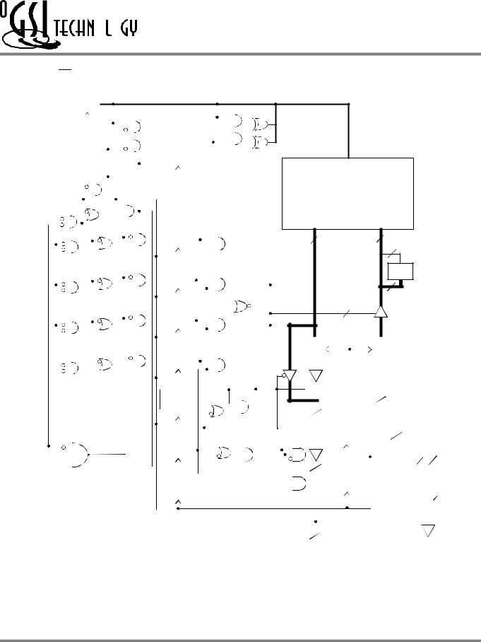
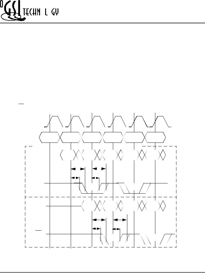
ByteSafe™ Parity Functions
In x32/x16 mode this RAM features a parity encoding and checking function. It is assumed that the RAM is being used in x32/x16 mode because there is no source for parity bits from the system. So, in x32/x16 mode, the device generates parity and stores it along with written data. It is also assumed that there is no facility for parity checking, so the RAM checks read parity and reports an error in the cycle following parity check.
In x32/x16 mode the device does not drive the 9th data output, even though the internal ByteSafe parity encoding has been activated. A ByteSafe SRAM, used in x32/x16 mode, allows parity protection of data in applications where parity encoding or checking are not otherwise available. As in any system that checks read parity, reads of un-written memory locations may well produce parity errors. Initialization of the memory should be implemented to avoid this issue.
In x18/x36 mode this SRAM includes a write data parity check that checks the validity of data coming into the RAM on write cycles. In Flow Through mode, write data errors are reported in the cycle following the data input cycle. In Pipeline mode, write data errors are reported one clock cycle later. (See timing diagram below.) The Data Parity Mode (DP) pin must be tied high to set the RAM to check for even parity or low to check for odd parity. Read data parity is not checked by the RAM as data validity is best established at the data’s destination. The Parity Error Output is an open drain output and drives low to indicate a parity error. Multiple Parity Error Output pins may share a common pull-up resistor.
x32 Mode (PE = 1) Read Parity Error Output Timing Diagram
Flow Through Mode
Pipelined Mode
CK |
|
|
|
|
|
|
|
|
|
|
|
|
|
|
|
|
|
|
|
|
|
|
|
|
|
|
|
|
|
|
|
|
|
|
|
|
|
|
|
|
|
|
|
||||||||||||
|
|
|
|
|
|
|
|
|
|
|
|
|
|
|
|
|
|
|
|
|
|
|
|
|
|
|
|
|
|
|
|
|
|
|
|
|
|
|
|
|
|
|
|
|
|
|
|
|
|
|
|
|
|
|
|
|
|
|
|
Address A |
|
|
Address B |
|
|
Address C |
|
Address D |
|
|
Address E |
||||||||||||||||||||||||||||||||||||||||
|
|
|
|
|
|
|
|
|
|
|
|
|
|
|
|
|
|
|
|
|
|
|
|
|
|
|
|
|
|
|
|
|
|
|
|
|
|
|
|
|
|
|
|
|
|
||||||||||
|
DQ |
|
|
|
|
|
|
|
|
D Out A |
|
D Out B |
D Out C |
|
D Out D |
||||||||||||||||||||||||||||||||||||||||
|
|
|
|
|
|
|
|||||||||||||||||||||||||||||||||||||||||||||||||
|
|
|
|
|
|
|
|
|
|
|
|
|
|
|
|
|
|
|
|
|
|
tKQ |
|
|
|
|
|
|
|
|
|
|
tHZ |
|
|
|
|
|
|
|
|
|
|
|
|
|
|
|
|
||||||
|
|
|
|
|
|
|
|
|
|
|
|
|
|
|
|
|
|
|
|
|
|
|
|
|
|
|
|
|
|
|
|
|
|
|
|
|
|
|
|
|
|
|
|
|
|
|
|
|
|
|
|
|
|
|
|
|
|
|
|
|
|
|
|
|
|
|
|
|
|
|
|
|
|
|
|
tLZ |
|
|
|
|
|
|
tKQX |
|
|
|
|
|
|
|
|
|
|
|
|
|
|
|
|
||||||||||||
|
|
|
|
|
|
|
|
|
|
|
|
|
|
|
|
|
|
|
|
|
|
|
|
|
|
|
|
|
|
|
|
|
|
|
|
|
|
|
|
|
|
|
|
|
|
|
|
|
|
|
|
|
|
|
|
|
|
|
|
|
|
|
|
|
|
|
|
|
|
|
|
|
|
|
|
|
|
|
|
|
|
|
|
|
|
|
|
|
|
|
|
|
|
|
|
|
|
|
|
|
|
|
|
|
|
|
|
|
|
|
|
QE |
Err A |
|
Err C |
|
|
||
DQ |
D Out A |
D Out B |
D Out C |
|
tKQ |
tHZ |
|
|
tLZ |
tKQX |
|
QE |
|
Err A |
|
|
|
|
Address F |
D Out E |
D Out D |
Err C
Rev: 1.15 5/2001 |
8/39 |
© 2000, Giga Semiconductor, Inc. |
Specifications cited are subject to change without notice. For latest documentation see http://www.gsitechnology.com.
Preliminary
GS88218/36B-11/11.5/100/80/66
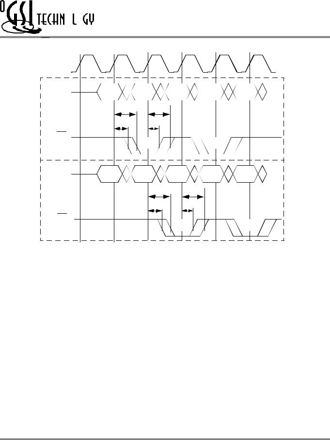
x18/x36 Mode (PE = 0) Write Parity Error Output Timing Diagram
Flow Through Mode
Pipelined Mode
CK |
|
|
|
|
DQ |
D In A |
D In B |
D In C |
D In D |
|
tKQ |
tHZ |
|
|
|
tLZ |
tKQX |
|
|
QE |
|
Err A |
|
Err C |
|
|
|
||
DQ |
D In A |
D In B |
D In C |
D In D |
|
|
tKQ |
tHZ |
|
|
|
tLZ |
tKQX |
|
QE |
|
|
Err A |
|
|
|
|
|
D In E |
D In E |
Err C
BPR 1999.05.18
Rev: 1.15 5/2001 |
9/39 |
© 2000, Giga Semiconductor, Inc. |
Specifications cited are subject to change without notice. For latest documentation see http://www.gsitechnology.com.

|
|
|
|
|
|
|
|
|
|
|
|
Preliminary |
|
|
|
|
|
|
|
|
|
|
GS88218/36B-11/11.5/100/80/66 |
||
|
|
|
|
|
|
|
|
|
|
|||
|
|
|
|
|
|
|
|
|
|
|
|
|
|
Mode Pin Functions |
|
|
|
|
|
|
|
|
|
||
|
|
|
|
|
|
|
|
|
||||
|
|
|
Mode Name |
Pin Name |
State |
Function |
|
|||||
|
|
|
|
|
|
|
|
|
|
|
|
|
|
|
|
|
|
|
|
|
|
|
|
|
|
|
|
|
|
|
|
|
|
|
L |
Linear Burst |
|
|
|
|
|
Burst Order Control |
|
LBO |
|||||||
|
|
|
|
|
|
|
|
|||||
|
|
|
|
H or NC |
Interleaved Burst |
|
||||||
|
|
|
|
|
|
|
|
|
|
|||
|
|
|
|
|
|
|
|
|
|
|
|
|
|
|
|
|
|
|
|
|
|
L |
Flow Through |
|
|
|
Output Register Control |
|
|
FT |
||||||||
|
|
|
|
|
|
|
||||||
|
|
|
H or NC |
Pipeline |
|
|||||||
|
|
|
|
|
|
|
|
|
|
|||
|
|
|
|
|
|
|
|
|
|
|
|
|
|
|
|
Power Down Control |
|
|
ZZ |
L or NC |
Active |
|
|||
|
|
|
|
|
|
|
|
|
||||
|
|
|
|
|
H |
Standby, IDD = ISB |
|
|||||
|
|
|
|
|
|
|
|
|
|
|||
|
Single / Dual Cycle Deselect Control |
SCD |
L |
Dual Cycle Deselect |
|
|||||||
|
|
|
|
|
||||||||
|
H or NC |
Single Cycle Deselect |
|
|||||||||
|
|
|
|
|
|
|
|
|
|
|||
|
|
|
|
|
|
|
|
|
|
|
|
|
|
ByteSafe Data Parity Control |
|
DP |
L |
Check for Odd Parity |
|
||||||
|
|
|
|
|
|
|||||||
|
|
H or NC |
Check for Even Parity |
|
||||||||
|
|
|
|
|
|
|
|
|
|
|||
|
|
|
|
|
|
|
|
|
|
|
|
|
|
|
|
|
|
|
|
|
|
L or NC |
Activate 9th I/Os (x18/36 Mode) |
|
|
|
|
|
Parity Enable |
|
PE |
|||||||
|
|
|
|
|
|
|
|
|||||
|
|
|
|
H |
Deactivate 9th I/Os (x16/32 Mode) |
|
||||||
|
|
|
|
|
|
|
|
|
|
|||
|
|
|
|
|
|
|
|
|
|
|
|
|
|
FLXDrive Output Impedance Control |
|
ZQ |
L |
High Drive (Low Impedance) |
|
||||||
|
|
|
|
|
|
|||||||
|
|
H or NC |
Low Drive (High Impedance) |
|
||||||||
|
|
|
|
|
|
|
|
|
|
|||
|
|
|
|
|
|
|
|
|
|
|
|
|
Note:
There are pull-up devices on the LBO, ZQ, SCD, DP and FT pins and a pull down device on the PE and ZZ pins, so those input pins can be unconnected and the chip will operate in the default states as specified in the above table.
Enable / Disable Parity I/O Pins
This SRAM allows the user to configure the device to operate in Parity I/O active (x18 or x36) or in Parity I/O inactive (x16 or x32) mode. Holding the PE bump low or letting it float will activate the 9th I/O on each byte of the RAM. Tying PE high deactivates the 9th I/O of each byte, although the bit in each byte of the memory array remains active to store and recall parity bits generated and read into the ByteSafe parity circuits.
Burst Counter Sequences
Linear Burst Sequence
|
A[1:0] |
A[1:0] |
A[1:0] |
A[1:0] |
|
|
|
|
|
|
|
|
|
|
1st address |
00 |
01 |
10 |
11 |
|
|
|
|
|
2nd address |
01 |
10 |
11 |
00 |
|
|
|
|
|
3rd address |
10 |
11 |
00 |
01 |
|
|
|
|
|
4th address |
11 |
00 |
01 |
10 |
|
|
|
|
|
Note: The burst counter wraps to initial state on the 5th clock.
Interleaved Burst Sequence
|
A[1:0] |
A[1:0] |
A[1:0] |
A[1:0] |
|
|
|
|
|
|
|
|
|
|
1st address |
00 |
01 |
10 |
11 |
|
|
|
|
|
2nd address |
01 |
00 |
11 |
10 |
|
|
|
|
|
3rd address |
10 |
11 |
00 |
01 |
|
|
|
|
|
4th address |
11 |
10 |
01 |
00 |
|
|
|
|
|
Note: The burst counter wraps to initial state on the 5th clock.
BPR 1999.05.18
Rev: 1.15 5/2001 |
10/39 |
© 2000, Giga Semiconductor, Inc. |
Specifications cited are subject to change without notice. For latest documentation see http://www.gsitechnology.com.
Preliminary
GS88218/36B-11/11.5/100/80/66
Byte Write Truth Table
|
|
|
|
|
|
|
|
|
|
|
|
|
|
|
|
|
|
|
|
Function |
GW |
BW |
|
BA |
|
BB |
BC |
BD |
Notes |
||||||||||
|
|
|
|
|
|
|
|
|
|
|
|
|
|
|
|
|
|
|
|
|
|
|
|
|
|
|
|
|
|
|
|
|
|
|
|
|
|
|
|
Read |
|
H |
|
H |
|
X |
|
X |
|
X |
|
X |
1 |
||||||
|
|
|
|
|
|
|
|
|
|
|
|
|
|
|
|
|
|
|
|
Read |
|
H |
|
L |
|
H |
|
H |
|
H |
|
H |
1 |
||||||
|
|
|
|
|
|
|
|
|
|
|
|
|
|
|
|
|
|
|
|
Write byte a |
|
H |
|
L |
|
L |
|
H |
|
H |
|
H |
2, 3 |
||||||
|
|
|
|
|
|
|
|
|
|
|
|
|
|
|
|
|
|
|
|
Write byte b |
|
H |
|
L |
|
H |
|
L |
|
H |
|
H |
2, 3 |
||||||
|
|
|
|
|
|
|
|
|
|
|
|
|
|
|
|
|
|
|
|
Write byte c |
|
H |
|
L |
|
H |
|
H |
|
L |
|
H |
2, 3, 4 |
||||||
|
|
|
|
|
|
|
|
|
|
|
|
|
|
|
|
|
|
|
|
Write byte d |
|
H |
|
L |
|
H |
|
H |
|
H |
|
L |
2, 3, 4 |
||||||
|
|
|
|
|
|
|
|
|
|
|
|
|
|
|
|
|
|
|
|
Write all bytes |
|
H |
|
L |
|
L |
|
L |
|
L |
|
L |
2, 3, 4 |
||||||
|
|
|
|
|
|
|
|
|
|
|
|
|
|
|
|
|
|
|
|
Write all bytes |
|
L |
|
X |
|
X |
|
X |
|
X |
|
X |
|
||||||
|
|
|
|
|
|
|
|
|
|
|
|
|
|
|
|
|
|
|
|
Notes:
1.All byte outputs are active in read cycles regardless of the state of Byte Write Enable inputs.
2.Byte Write Enable inputs BA, BB, BC, and/or BD may be used in any combination with BW to write single or multiple bytes.
3.All byte I/Os remain High-Z during all write operations regardless of the state of Byte Write Enable inputs.
4.Bytes “C” and “D” are only available on the x36 version.
Rev: 1.15 5/2001 |
11/39 |
© 2000, Giga Semiconductor, Inc. |
Specifications cited are subject to change without notice. For latest documentation see http://www.gsitechnology.com.

Preliminary
GS88218/36B-11/11.5/100/80/66
Synchronous Truth Table
|
Address |
State |
|
|
|
|
|
|
|
|
|
|
|
|
Operation |
Diagram |
E2 |
|
ADSP |
|
ADSC |
ADV |
W3 |
DQ4 |
|||||
Used |
|
|
||||||||||||
|
Key5 |
|
|
|
|
|
|
|
|
|
|
|
|
|
|
|
|
|
|
|
|
|
|
|
|
|
|
|
|
|
|
|
|
|
|
|
|
|
|
|
|
|||
Deselect Cycle, Power Down |
None |
X |
X |
|
X |
|
L |
|
X |
X |
High-Z |
|||
|
|
|
|
|
|
|
|
|
|
|
|
|||
Deselect Cycle, Power Down |
None |
X |
F |
|
L |
|
X |
|
X |
X |
High-Z |
|||
Deselect Cycle, Power Down |
None |
X |
F |
|
H |
|
L |
|
X |
X |
High-Z |
|||
|
|
|
|
|
|
|
|
|
|
|
|
|||
|
|
|
|
|
|
|
|
|
|
|
|
|
|
|
Read Cycle, Begin Burst |
External |
R |
T |
|
L |
|
X |
|
X |
X |
Q |
|||
Read Cycle, Begin Burst |
External |
R |
T |
|
H |
|
L |
|
X |
F |
Q |
|||
|
|
|
|
|
|
|
|
|
|
|
|
|||
|
|
|
|
|
|
|
|
|
|
|
|
|||
Write Cycle, Begin Burst |
External |
W |
T |
|
H |
|
L |
|
X |
T |
D |
|||
|
|
|
|
|
|
|
|
|
|
|
|
|||
|
|
|
|
|
|
|
|
|
|
|
|
|||
Read Cycle, Continue Burst |
Next |
CR |
X |
|
H |
|
H |
|
L |
F |
Q |
|||
|
|
|
|
|
|
|
|
|
|
|
|
|||
Read Cycle, Continue Burst |
Next |
CR |
X |
|
X |
|
H |
|
L |
F |
Q |
|||
|
|
|
|
|
|
|
|
|
|
|
|
|||
Write Cycle, Continue Burst |
Next |
CW |
X |
|
H |
|
H |
|
L |
T |
D |
|||
|
|
|
|
|
|
|
|
|
|
|
|
|||
Write Cycle, Continue Burst |
Next |
CW |
X |
|
X |
|
H |
|
L |
T |
D |
|||
|
|
|
|
|
|
|
|
|
|
|
|
|||
Read Cycle, Suspend Burst |
Current |
|
X |
|
H |
|
H |
|
H |
F |
Q |
|||
Read Cycle, Suspend Burst |
Current |
|
X |
|
X |
|
H |
|
H |
F |
Q |
|||
|
|
|
|
|
|
|
|
|
|
|
|
|||
Write Cycle, Suspend Burst |
Current |
|
X |
|
H |
|
H |
|
H |
T |
D |
|||
Write Cycle, Suspend Burst |
Current |
|
X |
|
X |
|
H |
|
H |
T |
D |
|||
|
|
|
|
|
|
|
|
|
|
|
|
|
|
|
Notes:
1.X = Don’t Care, H = High, L = Low
2.E = T (True) if E2 = 1; E = F (False) if E2 = 0
3.W = T (True) and F (False) is defined in the Byte Write Truth Table preceding.
4.G is an asynchronous input. G can be driven high at any time to disable active output drivers. G low can only enable active drivers (shown as “Q” in the Truth Table above).
5.All input combinations shown above are tested and supported. Input combinations shown in gray boxes need not be used to accomplish basic synchronous or synchronous burst operations and may be avoided for simplicity.
6.Tying ADSP high and ADSC low allows simple non-burst synchronous operations. See BOLD items above.
7.Tying ADSP high and ADV low while using ADSC to load new addresses allows simple burst operations. See ITALIC items above.
Rev: 1.15 5/2001 |
12/39 |
© 2000, Giga Semiconductor, Inc. |
Specifications cited are subject to change without notice. For latest documentation see http://www.gsitechnology.com.
 Loading...