

Page 1
Audio Service Manual
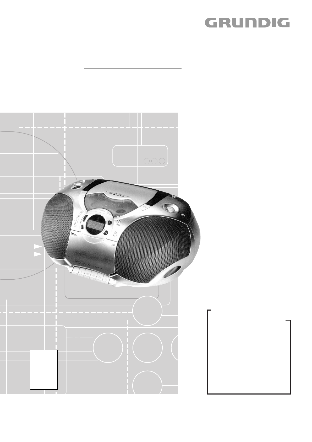
RR 740 CD
GDL5451
RR 770 CD
GDL5551
Zusätzlich erforderliche Unterlagen für den Komplettservice
Additionally required Service Documents for the Complete Service
Service
Manual
Sicherheit
Safety
Materialnr./Part No.
72010 800 0000
Materialnummer/Part Number 72010 771 1000
Änderungen vorbehalten/Subject to alteration • Printed in Germany ..
E-BS 32 0800 • 8002/8012, 8005/8015, 8006/8016
http://www.grundig.com
Grundig Service
Hotline Deutschland...
Technik:
TV
TV
SAT
VCR/LiveCam
HiFi/Audio
Car Audio
Telekommunikation
Planatron
Ersatzteil-Verkauf: ...Mo.-Fr. 8.00-19.00 Uhr
(8.00-22.00
...Mo.-Fr. 8.00-18.00 Uhr
0180/52318-41
0180/52318-49
0180/52318-48
0180/52318-42
0180/52318-43
0180/52318-44
0180/52318-45
Fax:
Telefon:
Fax:
0180/52318-51
0180/52318-99
Uhr)
0180/52318-40
0180/52318-50
Page 2

Allgemeiner Teil / General Section RR 740 CD / RR 770 CD
Es gelten die Vorschriften und Sicherheitshinweise gemäß dem Service Manual "Sicherheit",
Materialnummer 72010 800 0000, sowie zusätzlich die eventuell abweichenden, landesspezifischen Vorschriften!
Inhaltsverzeichnis
Seite
Allgemeiner Teil ........................... 1 - 2 … 1 - 12
Messgeräte/Messmittel .............................................................. 1 - 2
Service-Hinweise ....................................................................... 1 - 3
Technische Daten ...................................................................... 1 - 3
Bedienhinweise .......................................................................... 1 - 4
Ausbauhinweise ......................................................................... 1 - 8
Abgleichvorschriften ......................2 - 1 ... 2 - 3
Platinenabbildungen
und Schaltpläne ........................... 3 - 1 … 3 - 26
IC-Blockdiagramme ................................................................... 3 - 1
Verdrahtungsplan ....................................................................... 3 - 3
Schaltpläne:
CPU-Platte, Tastenplatte – RR 740 CD ................................. 3 - 5
CPU-Platte, Tastenplatte – RR 770 CD ................................. 3 - 9
Verstärkerplatte, Gleichrichterplatte,
Kopfhörerplatte – RR 740 CD .............................................. 3 - 11
Verstärkerplatte, Gleichrichterplatte,
Kopfhörerplatte – RR 770 CD .............................................. 3 - 15
Funktionsplatte – RR 740 CD .............................................. 3 - 17
Funktionsplatte – RR 770 CD .............................................. 3 - 19
Tuner-Platte, DSC-Schalterplatte,
Stereo/Mono-Schalter-Platte – RR 740 CD / RR 770 CD .......... 3 - 21
CD-Servo-Platte, CD-LED-Platte – RR 740 CD / RR 770 CD .... 3 - 25
Platinenabbildungen:
CPU-Platte,Tastenplatte – RR 740 CD ................................. 3 - 7
CPU-Platte,Tastenplatte – RR 770 CD ................................. 3 - 8
Verstärkerplatte, Kopfhörerplatte,
Gleichrichterplatte – RR 740 CD ............................................ 3 - 13
Verstärkerplatte, Kopfhörerplatte,
Gleichrichterplatte – RR 770 CD ............................................ 3 - 14
Funktionsplatte – RR 740 CD .............................................. 3 - 18
Funktionsplatte – RR 770 CD .............................................. 3 - 20
Tuner-Platte – RR 740 CD / RR 770 CD .................................. 3 - 23
Stereo/Mono-Schalter-Platte – RR 740 CD / RR 770 CD .......... 3 - 23
CD-LED-Platte – RR 740 CD / RR 770 CD .............................. 3 - 23
DSC-Schalterplatte – RR 740 CD / RR 770 CD ........................ 3 - 23
CD-Servo-Platte – RR 740 CD / RR 770 CD ............................ 3 - 24
The regulations and safety instructions shall be
valid as provided by the "Safety" Service Manual,
part number 72010 800 0000, as well as the
respective national deviations!
Table of Contents
Page
General Section ............................ 1 - 2 … 1 - 12
Measuring Instruments/Equipment ............................................ 1 - 2
Service Hints .............................................................................. 1 - 3
Technical Data ........................................................................... 1 - 3
Operating Hints .......................................................................... 1 - 6
Disassembly Instructions ........................................................... 1 - 8
Adjustment Procedures..................2 - 4 ... 2 - 6
Layout of the PCBs
and Circuit Diagrams ................... 3 - 1 … 3 - 26
IC Block Diagrams ..................................................................... 3 - 1
Wiring Diagram .......................................................................... 3 - 3
Circuit Diagrams:
CPU Board, Key Board – RR 740 CD .................................... 3 - 5
CPU Board, Key Board – RR 770 CD .................................... 3 - 9
Amplifier Board, Rectifier Board,
Headphone Board – RR 740 CD .......................................... 3 - 11
Amplifier Board, Rectifier Board,
Headphone Board – RR 770 CD .......................................... 3 - 15
Function Board – RR 740 CD .............................................. 3 - 17
Function Board – RR 770 CD .............................................. 3 - 19
Tuner Board, DSC Switch Board,
Stereo/Mono Switch Board – RR 740 CD / RR 770 CD ............. 3 - 21
CD Servo Board, CD LED Board – RR 740 CD / RR 770 CD .... 3 - 25
Layout of the PCBs:
CPU Board, Key Board – RR 740 CD ................................... 3 - 7
CPU Board, Key Board – RR 770 CD ................................... 3 - 8
Amplifier Board, Headphone Board,
Rectifier Board – RR 740 CD .................................................. 3 - 13
Amplifier Board, Headphone Board,
Rectifier Board – RR 770 CD .................................................. 3 - 14
Function Board – RR 740 CD .............................................. 3 - 18
Function Board – RR 770 CD .............................................. 3 - 20
Tuner Board – RR 740 CD / RR 770 CD ................................... 3 - 23
Stereo/Mono Switch Board – RR 740 CD / RR 770 CD ............. 3 - 23
CD LED Board – RR 740 CD / RR 770 CD .............................. 3 - 23
DSC Switch Board – RR 740 CD / RR 770 CD ......................... 3 - 23
CD Servo Board– RR 740 CD / RR 770 CD ............................. 3 - 24
Explosionszeichnungen und
Ersatzteillisten ................................ 4 - 1 … 4 - 6
Allgemeiner Teil
Messgeräte/Messmittel
Frequenzzähler, NF-Voltmeter, Tonhöhenschwankungsmesser,
Messsender, Wobbelsender, Oszilloskop, Digitalvoltmeter, FETestcassette 3150Hz/8000Hz, Test-CD (z.B. 5A)
Beachten Sie bitte das GRUNDIG Messtechnik-Programm, das Sie
unter folgender Adresse erhalten:
GRUNDIG Instruments Test- und Messsysteme GmbH
Würzburger Str. 150, D 90766 Fürth/Bay
Tel. 0911/703-4118, Fax 0911/703-4130
eMail: instruments@grundig.de, Internet: http://www.grundig-instruments.de
1 - 2 GRUNDIG Service
Exploded Views and
Spare Parts Lists ............................ 4 - 1 … 4 - 6
General Section
Measuring Instruments/Equipment
Frequency counter, AF voltmeter, Wow and flutter meter, Signal
generator, Sweep generator, Oscilloscope, Digital voltmeter, FE Test
cassette 3150Hz/8000Hz, Test CD (e.g. 5A)
Please note the GRUNDIG Catalog "Test and Measuring Equipment"
obtainable from:
Page 3
Allgemeiner Teil / General SectionRR 740 CD / RR 770 CD
Servicehinweise
Cassettenteil
Überprüfen Sie vor Beginn der Service-Arbeiten, ob die Magnetköpfe,
die Tonwelle und die Gummiandruckrolle frei von Bandabrieb sind.
Zum Reinigen dieser Teile verwenden Sie ein mit Spiritus oder Reinigungsbenzin getränktes Wattestäbchen; dadurch verbessert sich der
Aufnahme- und Wiedergabepegel, sowie der Bandlauf.
Nach dem Ersatz von Magnetköpfen oder sonstiger Bauteile müssen
die technischen Daten des Gerätes anhand der im Service Manual
vorgegebenen Messwerte überprüft bzw. eingestellt werden.
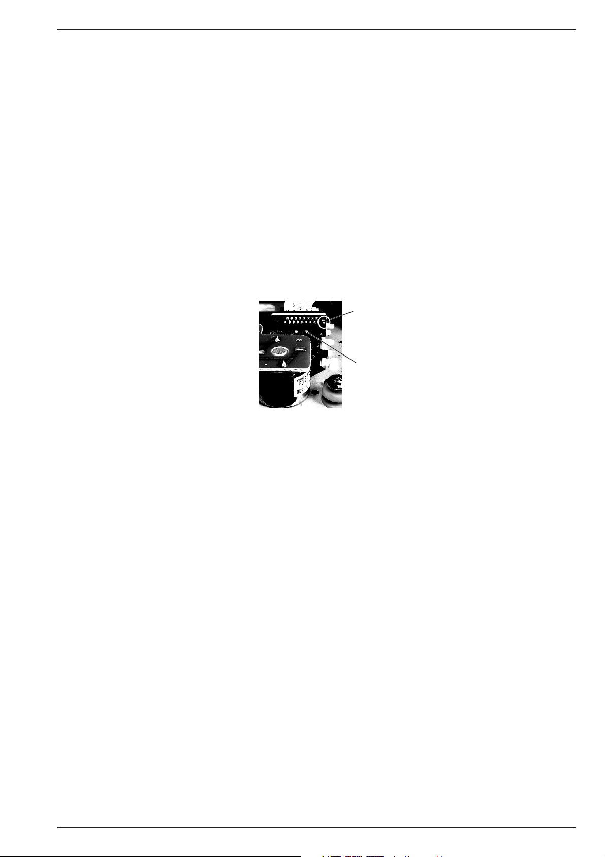
CD-Teil
Bei Ausbau der CD-Lasereinheit muss vor Abziehen der Steckverbindungen eine Schutzlötstelle auf der Leiterplatte der
Lasereinheit angebracht werden, um eine Zerstörung der Laserdiode durch statische Aufladung zu vermeiden.
Beim Einbau einer neuen Lasereinheit (CD-Laufwerk) muss
nach Einstecken der Steckverbinder die werkseitig angebrachte
Schutzlötstelle entfernt werden!
Service Hints
Cassette Section
Before commencing service work, ensure that the magnetic heads, the
capstan and the pinch roller are free from particles produced by tape
abrasion. The recording and playback levels and the tape run can be
improved by cleaning these parts with a cotton-wool tip soaked in spirit
or cleaning benzine.
If the heads or other components have been replaced, the technical
data of the recorder must be checked or adjusted according to the
values specified in the Service Manual.
CD Section
When removing the Laser pick-up, the Laser pick-up PCB must be
provided with a protective soldered joint before unplugging the
connectors to avoid damage to the Laser diode by static charges.
When inserting the new Laser pick-up (CD drive mechanism) the
soldered joint fitted at the factory must be removed after the
connectors are plugged in.
Schutzlötstelle
protective soldered joint
Technische Daten
Spannungsversorgung:
Netzbetrieb ............................................................... 230V, 50/60Hz
Batteriebetrieb ................................................. 8 x 1,5V (R20, UM1)
Stützbatterie ............................................... 2 x 1,5 Volt (LR 06, AA)
Fernbedienung (nur RR 770):
Typ Micro ................................................ z.B. AAA LR 03, 2 x 1,5V
Verstärkerteil:
Ausgangsleistung (DIN 45324, 10% THD):
Musikleistung ...................................................................... 2 x 4,5W
Sinusleistung ....................................................................... 2 x 2,5W
Stereo-Kopfhörer-Klinkenbuchse ........................................ 3,5mm ø
Rundfunkteil:
Wellenbereiche .................................................... FM 87,5 - 108MHz
MW 522 - 1620kHz
LW 146 - 281kHz
Antennen.................................................... Teleskopantenne für FM
eingebaute Ferritstab-Antenne für MW/LW
Cassettenteil:
Tonträger .................. Fe/IEC1, Compact-Cassette nach DIN 45516
Spurlage ....................................................... Viertelspur international
Bandgeschwindigkeit ..................................................... 4,76cm/sec.
Motor ..................................................................... Gleichstrommotor
Frequenzübertragungsbereich .....................................125Hz - 8kHz
Geräuschspannungsabstand (bewertet) ................................... 45dB
Gleichlauffehler .................................................................... < 0,35%
Automatik ........................... Aussteuerungsautomatik bei Aufnahme,
Automatisches Auslösen der Tasten am Bandende
CD-Teil:
Frequenzübertragungsbereich .....................................20Hz - 20kHz
Geräuschspannungsabstand ................................................. > 68dB
Laseranschlußplatte
Laser PCB
Technical Data
Power Supply:
Mains operation ........................................................ 230V, 50/60Hz
Battery operation ............................................. 8 x 1.5V (R20, UM1)
Back-up battery ............................................2 x 1.5 Volt (LR 06, AA)
Remote control (RR 770 only):
Micro type ................................................. e.g. AAA LR 03, 2 x 1.5V
Amplifier Section:
Output power (DIN 45324, 10% THD):
Music power ....................................................................... 2 x 4.5W
Nominal power .................................................................... 2 x 2.5W
Jack socket for stereo headphones ................................... 3.5mm ø
Radio Section:
Waveband ............................................................FM 87.5 - 108MHz
MW 522 - 1620kHz
LW 146 - 281kHz
Aerials ......................................................... Telescopic aerial for FM
Built in ferrite rod aerial for MW/LW
Cassette Section:
Cassette......................... Fe/IEC1, Compact cassette to DIN 45516
Track System ............................................International quartertrack
Tape Speed ................................................................... 4.76cm/sec.
Motor .................................................................................. DC motor
Frequency Range ........................................................125Hz - 8kHz
S/N Ratio (weighted) ................................................................ 45dB
Wow and Flutter .................................................................. < 0.35%
Automatic ..................................... Automatic recording level control
Automatic button release at tape end
CD Section:
Frequency range ......................................................... 20Hz - 20kHz
S/N ratio, weighted ................................................................ > 68dB
GRUNDIG Service 1 - 3
Page 4
Allgemeiner Teil / General Section RR 740 CD / RR 770 CD
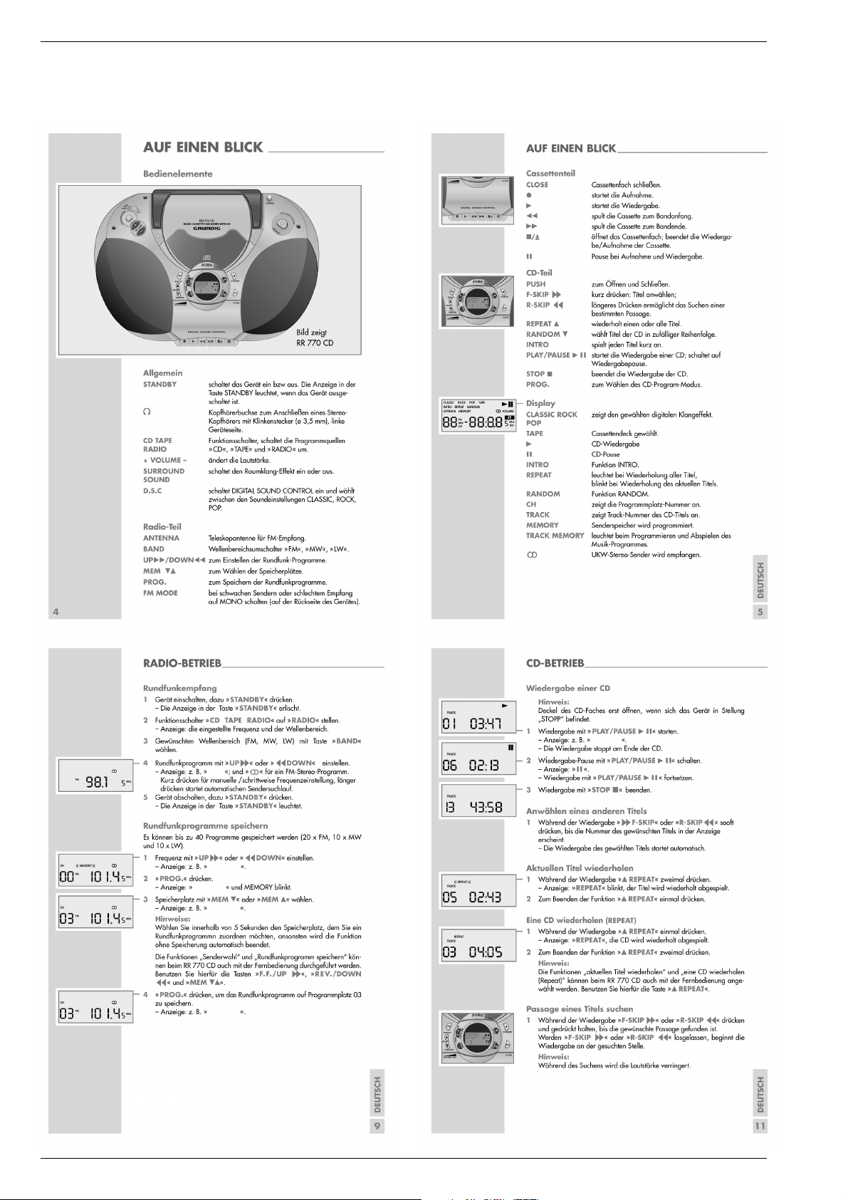
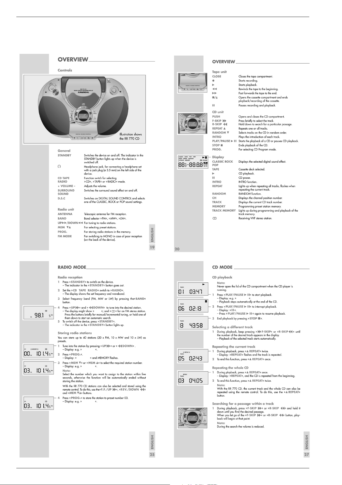
Bedienhinweise
Dieses Kapitel enthält Auszüge aus der Bedienungsanleitung. Weitergehende Informationen entnehmen Sie bitte der gerätespezifischen
Bedienungsanleitung, deren Materialnummer Sie in der entsprechenden Ersatzteilliste finden.
1 - 4 GRUNDIG Service
Page 5
RR 740 CD / RR 770 CD Allgemeiner Teil / General Section
GRUNDIG Service 1 - 5
Page 6
Allgemeiner Teil / General Section RR 740 CD / RR 770 CD
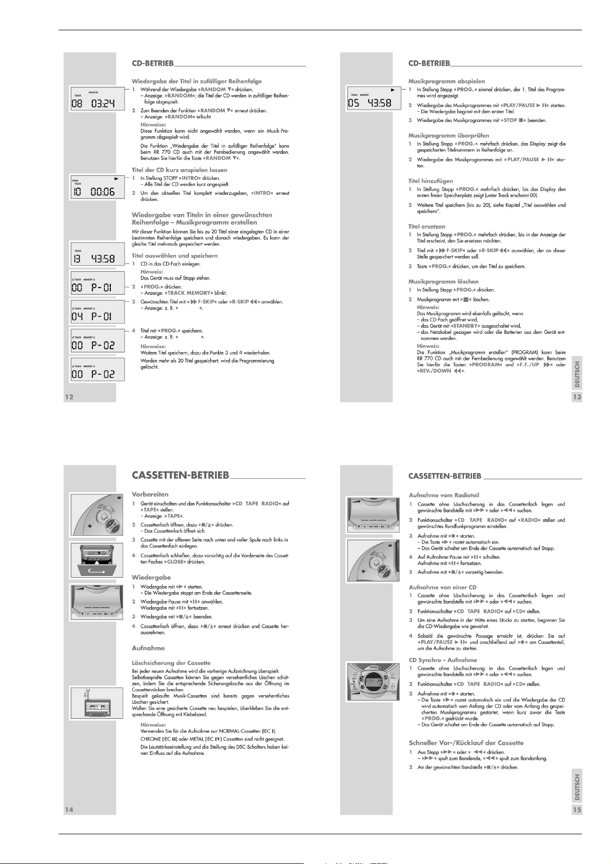
Operating Hints
This chapter contains excerpts from the operating instructions. For further particulars please refer to the appropriate user instructions the part number
of which is indicated in the relevant spare parts list.
1 - 6 GRUNDIG Service
Page 7
RR 740 CD / RR 770 CD Allgemeiner Teil / General Section
GRUNDIG Service 1 - 7
Page 8
Allgemeiner Teil / General Section RR 740 CD / RR 770 CD
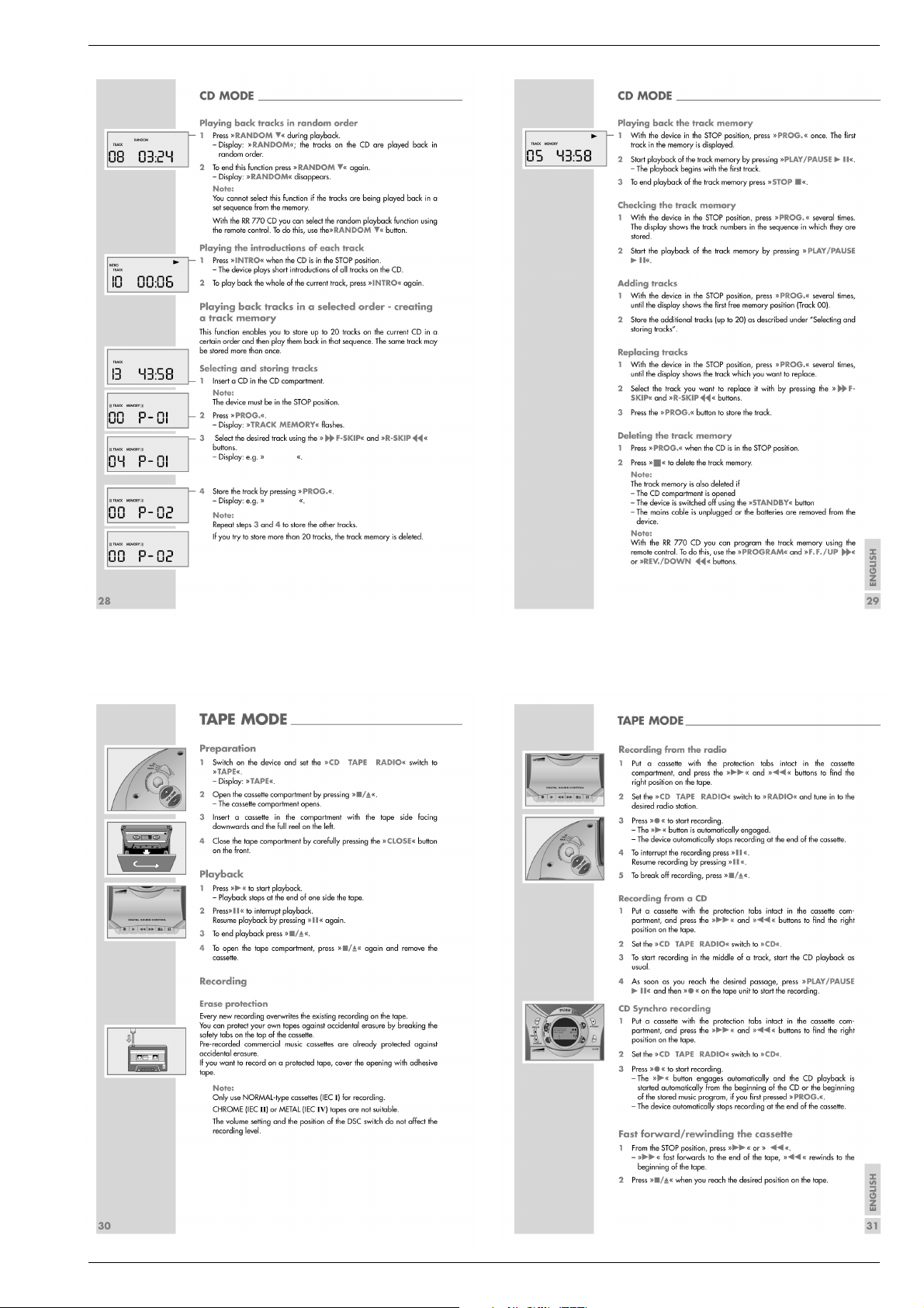
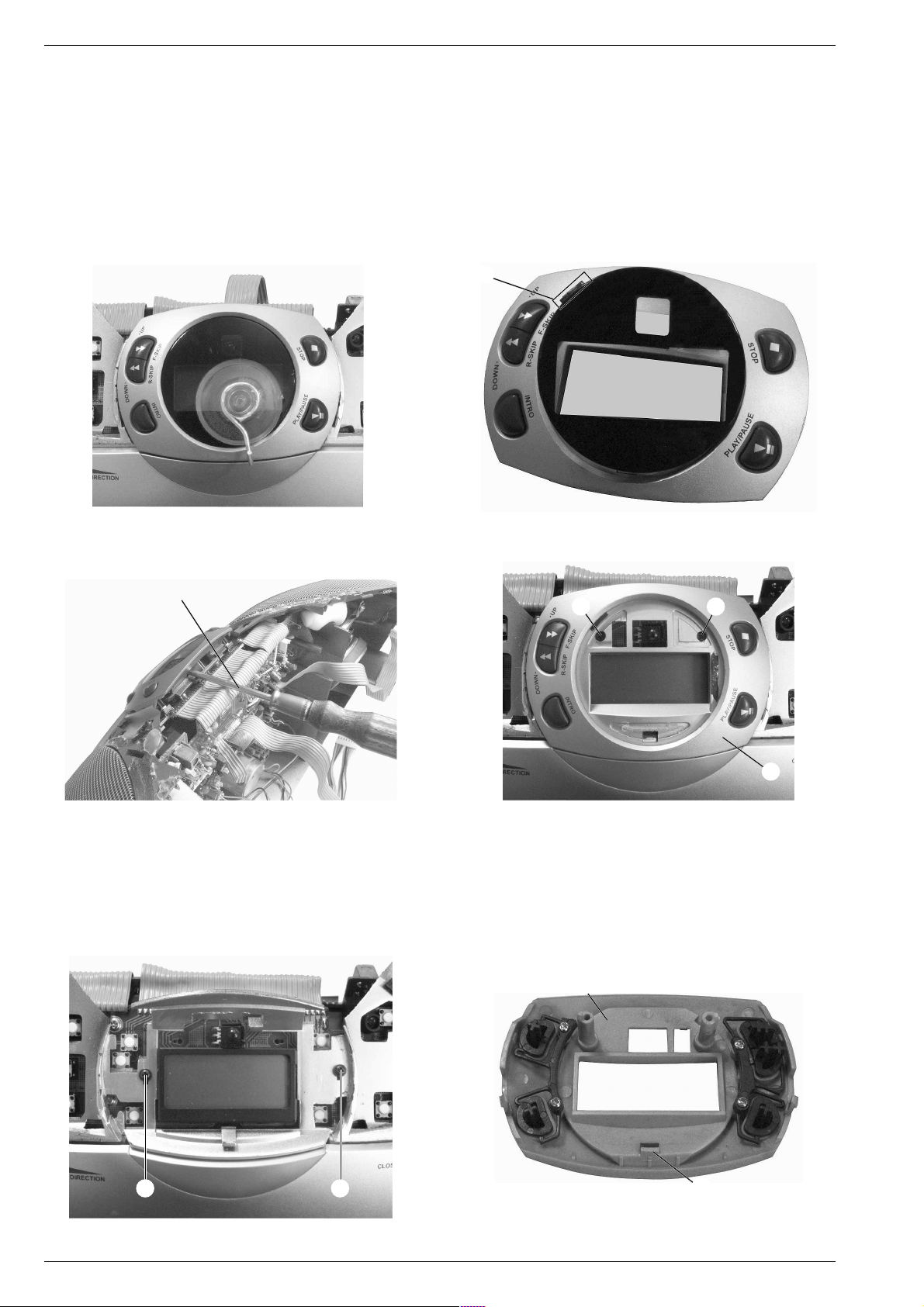
Ausbauhinweise
1. Gehäuserückwand abnehmen
- Schraube B (Fig. 1) herausdrehen und Antenne nach oben aus
dem Gehäuse ziehen.
- 13 Schrauben A (Fig. 1) herausdrehen.
- Gehäusevorderteil und Gehäuserückteil vorsichtig ca. 5cm auseinanderziehen.
- Bei Bedarf Steckverbindungen lösen und Gehäuserückteil abnehmen.
A
Disassembly Instructions
1. Removing the Rear of the Cabinet
- Undo the screw B (Fig. 1) and pull out the aerial.
- Undo the 13 screws A (Fig. 1).
- Carefully pull apart the front and rear cabinet parts by about 5cm.
- If necessary undo the connectors and remove the rear cabinet parts.
A
B
E
C
C
E
G
Fig. 1
G
D
F
D
Klebestellen
glued joints
Fig. 3 Fig. 4Fig. 2
1 - 8 GRUNDIG Service
Klebestellen
glued joints
Page 9
Allgemeiner Teil / General SectionRR 740 CD / RR 770 CD
2. Gehäuseoberteil abnehmen
- Gehäuserückwand abnehmen (Pkt. 1).
- 2 Schrauben E und Schraube F herausdrehen (Fig. 3).
- Die beiden Abdeckungen G (Fig. 3) abnehmen und die darunter
liegenden Schrauben herausdrehen.
- Schraube H herausdrehen (Fig. 5).
- Abdeckungen C und D (Fig. 2, 3 und 4) abnehmen:
Die Abdeckungen werden durch Rastnasen gehalten und sind
zusätzlich an den markierten Stellen verklebt. Abdeckungen C
und D an den Punkten I (Fig. 6 und 7) vorsichtig abhebeln . Diese
Abdeckungen vorsichtig nach oben biegen (bei Bedarf die Abdekkungen durch vorsichtiges Abhebeln ganz abnehmen) und
Gehäuseoberteil herausziehen (Fig. 8 und 9). Wenden Sie zuviel
Kraft auf, können Rastnasen oder die Blende brechen! In Fig. 2 und
4 sehen Sie die Anordnung der Rastnasen.
- Steckverbindungen nach Bedarf lösen.
2. Removing the Top of the Cabinet
- Remove the rear of the cabinet (para 1).
- Undo the 2 screws E and the screw F (Fig. 3).
- Remove the two covers G (Fig. 3) then undo the screws located
below.
- Undo the screw H (Fig. 5).
- Remove the covers C and D (Fig. 2, 3 and 4):
The covers are held in place by locking lugs and are in addition
glued at the marked spots. Carefully lift off the covers C and D at
the points I (Fig. 6 and 7). Carefully bend up these covers (if
necessary remove the covers completely by carefully lifting them
off) then pull out the top part of the cabinet (Fig. 8 and 9). If you apply
too much force the locking lugs or the trimplate might break! Fig. 2
and 4 show the locations of the locking lugs.
- If necessary undo the connectors.
H
D
D
Fig. 5
I
Fig. 6 Fig. 7
I
C
C
Fig. 8 Fig. 9
GRUNDIG Service 1 - 9
Page 10
Allgemeiner Teil / General Section RR 740 CD / RR 770 CD
3. Bedienteil ausbauen
- Gehäuseoberteil abnehmen (Pkt. 2).
- Das aufgeklebte Display-Fenster mit Hilfe eines geeigneten Saugknopfes, wie in Fig. 10 gezeigt, nach vorne abziehen.
Es ist zu beachten, dass wegen der Führungsnase J (Fig. 11) am
linken oberen Rand des Display-Fensters der Saugknopf möglichst
am rechten unteren Rand des Fensters angebracht wird.
Steht kein geeigneter Saugknopf zur Verfügung, kann das Display-Fenster mit Hilfe eines geeigneten Werkzeuges (z. B. kleiner
Schraubendreher ohne scharfkantige Klinge), wie in Fig. 12
gezeigt, vorsichtig von hinten durchgedrückt werden. Dabei kann
das Fenster beschädigt werden.
3. Removing the Control Unit
- Remove the top of the cabinet (para 2).
- Pull off the glued-on display window toward the front using an
appropriate sucker as shown in Fig. 10.
In order to not interfere with the guide lug J (Fig. 11) at the left top
border of the display window, the sucker must be applied at the right
bottom border of the window.
If no appropriate sucker is available, it is possible to carefully push
out the window from the rear using an appropriate tool (e.g. a small
screwdriver or a sharp-edged blade) as shown in Fig. 12. In doing
this, the window may be damaged.
J
Fig. 10 Fig. 11
Schraubendreher
screwdriver
Fig. 12 Fig. 13
- 2 Schrauben K herausdrehen (Fig. 13).
- Blende L (Fig. 13 und 15) vorsichtig nach vorne abziehen. Dabei
darf sie nicht nach oben gedrückt werden, da sonst die Führungsnase M (Fig. 15) an der Blende L (Fig. 15) abbrechen kann.
- 2 Schrauben N herausdrehen (Fig. 14).
K K
L
- Undo the 2 screws K (Fig. 13).
- Carefully pull off the trimplate L to the front (Fig. 13 and 15)
preventing it from being bent up as otherwise the guide lug M
(Fig. 15) on the trimplate L (Fig. 15) might break off.
- Undo the 2 screws N (Fig. 14).
L
N N
Fig. 14 Fig. 15
1 - 10 GRUNDIG Service
M
Page 11
Allgemeiner Teil / General SectionRR 740 CD / RR 770 CD
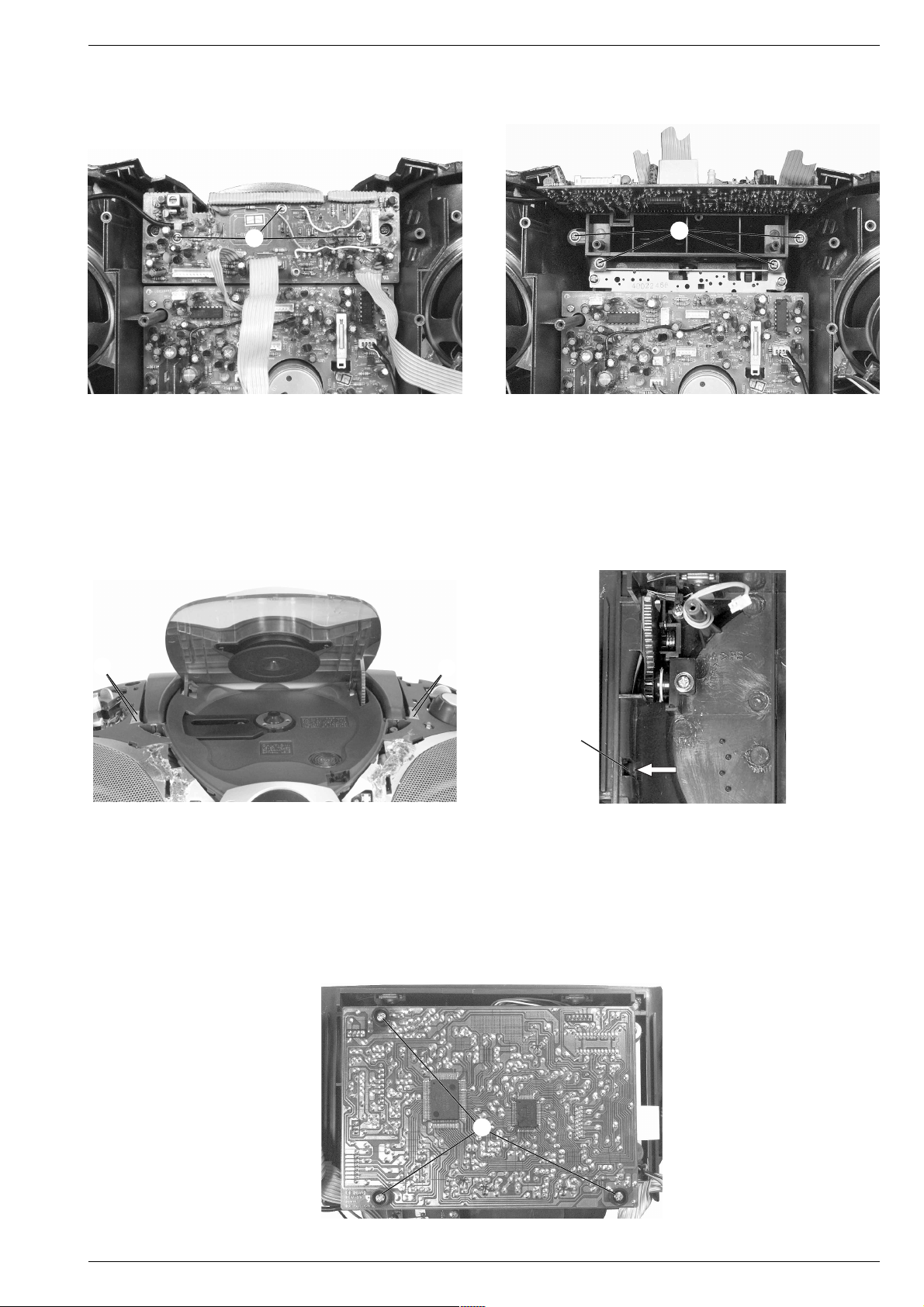
- 3 Schrauben O (Fig. 16) herausdrehen und CPU-Platte nach oben
klappen.
- 4 Schrauben P (Fig. 17) herausdrehen und Bedienteil mit Halterung
herausnehmen.
O
Fig. 16 Fig. 17
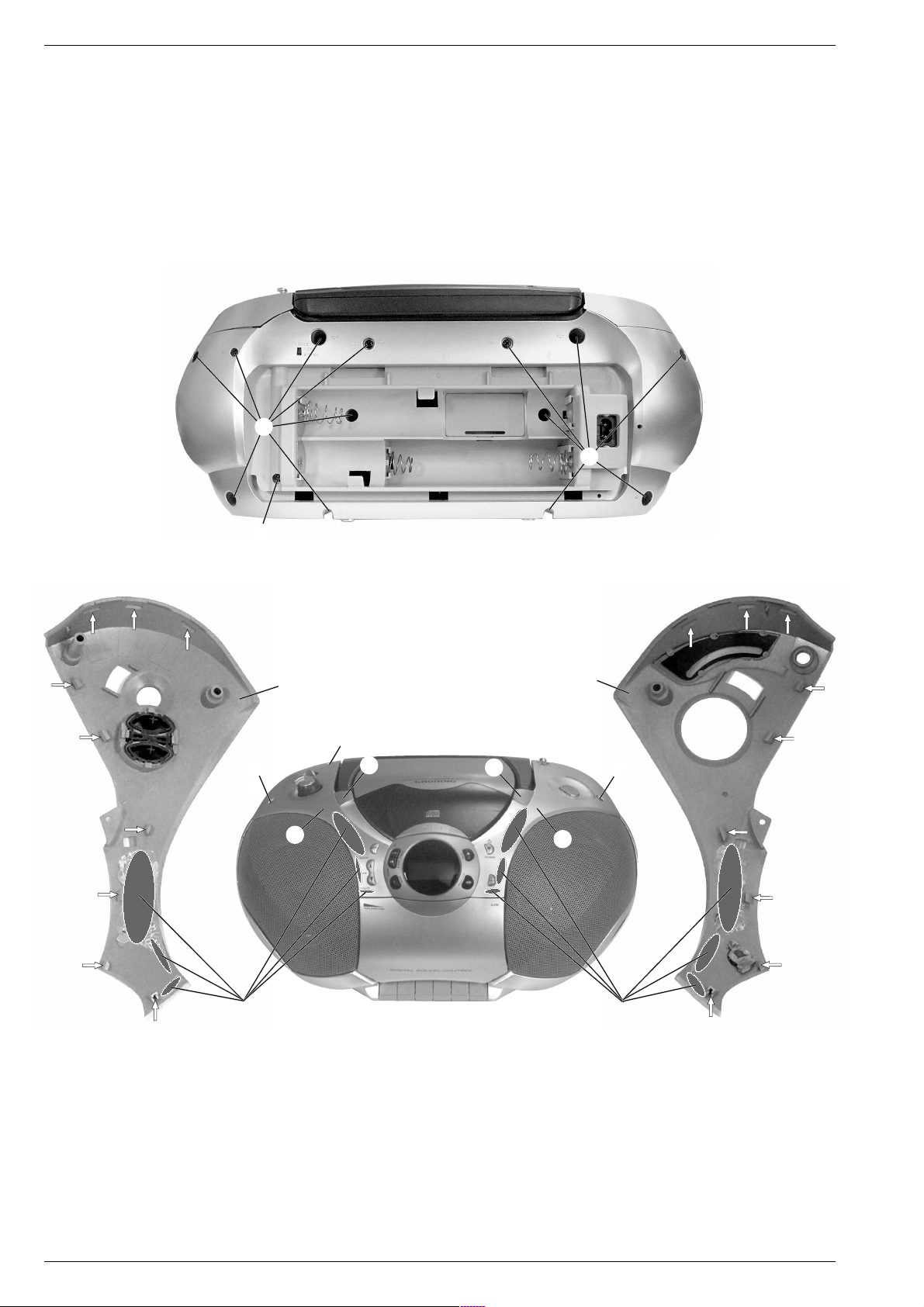
4. Griff ausbauen
- Gehäuseoberteil abnehmen (Pkt. 2).
- CD-Laufwerk ausbauen (Pkt. 6).
- 4 Schrauben Q (Fig. 18) herausdrehen, die beiden Abdeckungen
und die darunter liegenden Plättchen herausnehmen.
- Griff nach oben klappen und durch Eindrücken der FührungsBolzen R auf beiden Seiten des Griffes ausrasten (Fig. 19).
- Undo the 3 screws O (Fig. 16) then tilt up the CPU PCB.
- Undo the 4 screws P (Fig. 17) then remove the control unit together
with its holder.
P
4. Removing the Handle
- Remove the top of the cabinet (para 2).
- Remove the CD drive unit (para 6).
- Undo the 4 screws Q (Fig. 18) then remove the two covers and the
small plates located below.
- Tilt the handle up then disengage it by pressing on the guide lugs R
located at the sides of the handle (Fig. 19).
Q
Fig. 18 Fig. 19
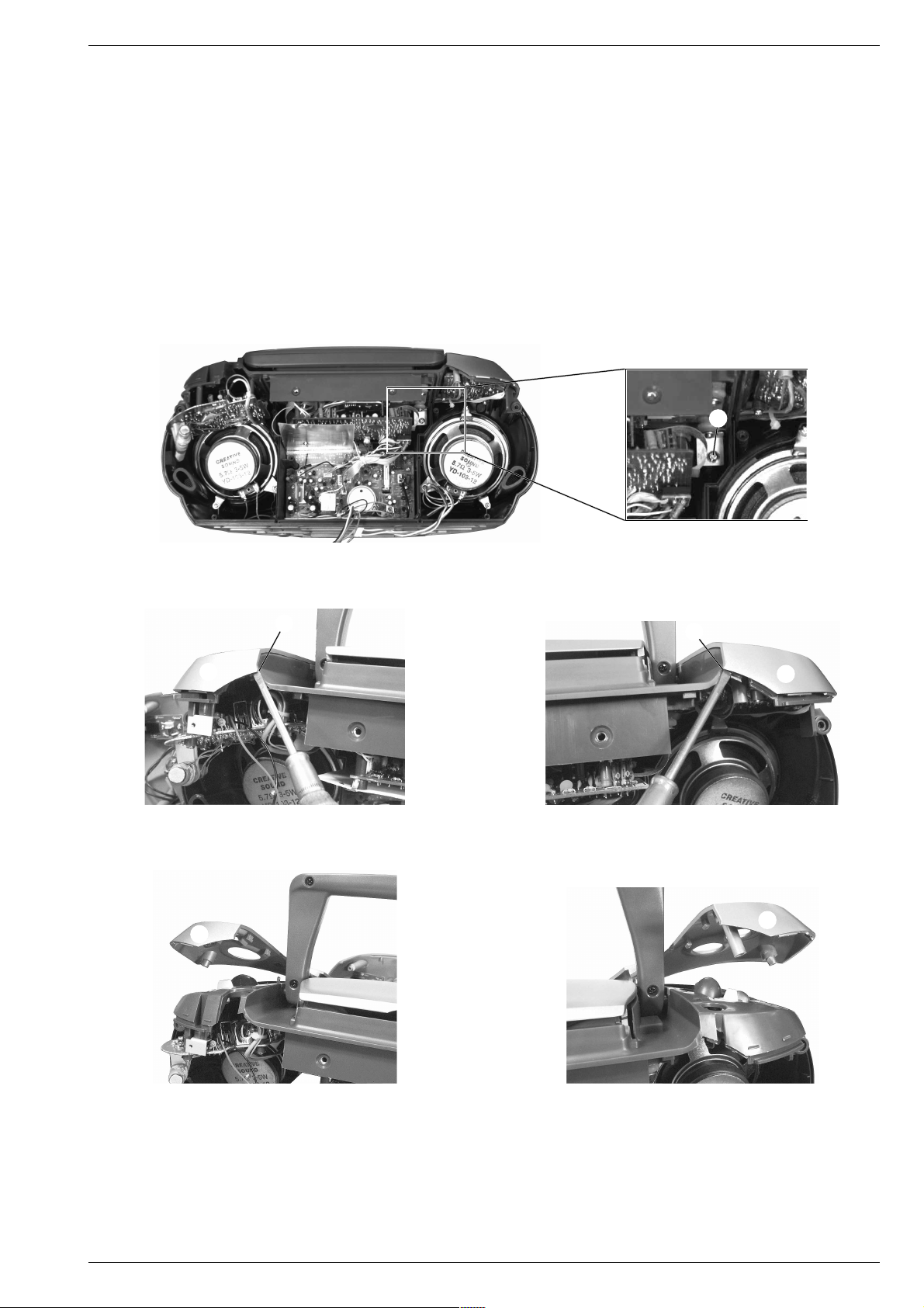
5. CD-Servo-Platine ausbauen
- Gehäuserückwand abnehmen (siehe Pkt. 1).
- 3 Schrauben S herausdrehen (Fig. 20).
- Hinweis: Vor Abziehen der Flexprintleitung die Sicherungslötstelle
U (Fig. 21) des Lasers kurzschließen (Siehe Seite 1-3
Allgemeiner Teil / Servicehinweise / CD-Teil).
- Platine herausnehmen, gegebenfalls Steckverbinder lösen.
Q
R
5. Removing the CD Servo Board
- Remove the rear of the cabinet (para 1).
- Undo the 3 screws S (Fig. 20).
- Note: Prior to pulling off the Flexprint lead shortcircuit the protective
soldering joint U (Fig. 21) of the laser (Page 1-3 General
Section / Service Hints / CD Section).
- Remove the PCB. If necessary, undo the connector.
S
Fig. 20
GRUNDIG Service 1 - 11
Page 12
Allgemeiner Teil / General Section RR 740 CD / RR 770 CD
V
U
Fig. 21 Fig. 22
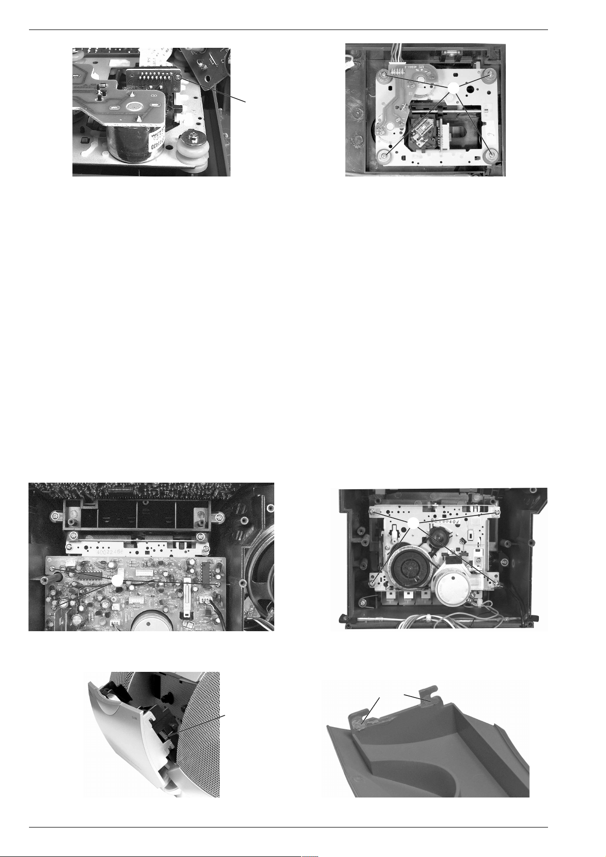
6. CD-Laufwerk ausbauen
- Gehäuserückwand abnehmen (siehe Pkt. 1).
- CD-Servo Platine ausbauen (siehe Pkt. 5).
- 4 Schrauben V herausdrehen (Fig. 22) und CD-Laufwerk herausnehmen, dabei Steckverbinder nach Bedarf öffnen.
7. Cassetten-Laufwerk ausbauen
- Gehäuseoberteil abnehmen (Pkt. 2).
- 3 Schrauben O (Fig. 16) herausdrehen und CPU-Platte nach oben
klappen.
- 3 Schrauben W herausdrehen (Fig. 23) und Hauptplatte herausnehmen.
- Cassettenfach öffnen, 4 Schrauben X herausdrehen (Fig. 24) und
Laufwerk herausnehmen.
Hinweis: Beim Einbau des Cassetten-Laufwerkes ist darauf zu
achten, dass die Tastenstößel des Cassetten-Laufwerkes in den
Nuten der Bedientasten eingreifen.
8. Cassetten-Blende ausbauen
- Cassettenfach öffnen.
- Die Rastnase Y (Fig. 25) auf der nicht verklebten Seite nach innen
drücken und Cassetten-Blende auf dieser Seite ausrasten. Die
Cassetten-Blende auf der nicht verklebten Seite soweit nach vorne
ziehen, dass die verklebte Seite der Blende vorsichtig zur Seite
weggedrückt werden kann.
6. Removing the CD Drive Unit
- Remove the rear of the cabinet (para 1).
- Remove the CD servo board (para 5).
- Undo the 4 screws V (Fig. 22) then remove the CD drive unit. If
necessary undo the connectors.
7. Removing the Cassette Drive Unit
- Remove the top of the cabinet (para 2).
- Undo the 3 screws O (Fig. 16) then tilt up the CPU PCB.
- Undo the 3 screws W (Fig. 23) then remove the main PCB.
- Open the cassette compartment, undo the 4 screws X (Fig. 24) then
remove the drive unit.
Note: When refitting the cassette drive unit the slides of the cassette
drive unit must engage into the grooves of the control buttons.
8. Removing the Cassette Trimplate
- Open the cassette compartment.
- Press in the locking lug Y (Fig. 25) at its side not fixed with glue then
disengage the cassette trimplate at this side. Pull the cassette
trimplate at the side without glued joints to the front until the glued
side of the trimplate can be carefully pressed apart.
W
X
Fig. 23 Fig. 24
Klebestellen
glued joints
Y
Fig. 25 Fig. 26
1 - 12 GRUNDIG Service
Page 13

Abgleichvorschriften / Adjustment ProceduresRR 740 CD / RR 770 CD
Abgleichvorschriften
1. Cassettenteil
Messgeräte/Messmittel: Frequenzzähler, NF-Voltmeter, Tonhöhenschwankungsmesser, Fe-Testcassette 3150Hz/8000Hz (z.B. 449).
Abgleich Vorbereitung Abgleichvorgang
1. Bandgeschwindigkeit
2. Gleichlauf
4. Kopfspaltsenkrechtstellung
(Azimut)
5. Vormagnetisierungsfrequenz
Verstärkerplatte
Frequenzzähler an Kopfhörerbuchse.
Testcassette einlegen, 3150Hz abspielen.
Tonhöhenschwankungsmesser an Kopfhörerbuchse.
Testcassette einlegen, 3150Hz abspielen.
NF-Voltmeter an Kopfhörerbuchse.
Testcassette einlegen, 8kHz abspielen.
Frequenzzähler an Stecker CN403A Pin 2 / Pin 4(Masse).
Bespielbare Cassette einlegen.
Gerätefunktion: Aufnahme-Start.
Mit dem Einstellregler (im Cass.-Motor)
3150Hz ± 0,1% einstellen.
Bandgeschw.
Tape speed
Gleichlaufabweichung ≤ 0,35% (gehörrichtig bewertet).
Wiedergabemeßzeit ≥ 30 Sekunden.
Mit der Kopfeinstellschraube 1
den linken und rechten Kanal auf
1
Pegelmaximum einstellen.
Der Pegelunterschied von Kanal zu
Kanal darf maximal 3dB betragen.
Mit L401 63kHz ± 0,5kHz einstellen.
2. DC/DC-Converter
Messgeräte/Messmittel: Frequenzzähler
Abgleich Vorbereitung Abgleichvorgang
1. ConverterFrequenz
Frequenzzähler an Meßpunkt
TP
CPU Platte
.
TP
Mit L103 2,7MHz ± 0,1MHz einstellen.
L.CH
R.CH
4
1
PIN 4
PIN 2
GRUNDIG Service 2 - 1
Page 14

Abgleichvorschriften / Adjustment Procedures RR 740 CD / RR 770 CD
3. Tuner
Messgeräte: Messsender, Wobbelsender, Oszilloskop, Digitalvoltmeter.
Funktionsschalter: Radio
Abgleich Vorbereitung Abgleichvorgang
1. AM-ZF
2. MW-Oszillator
3. MW-Vorkreis
4. LW-Oszillator
5. LW-Vorkreis
6. FM-ZF
Wobbelsender 450kHz über Rahmenantenne in L503
(Ferritantenne) einkoppeln.
Oszilloskop an Messpunkt
(IC502 Pin 18).
TP 5
Bandschalter: MW
MW, 1620kHz
Digitalvoltmeter an Messpunkt
(CN501 Pin 9).
TP 6
Bandschalter: MW
MW 612kHz, MW 1404kHz
Messsendersignal über Rahmenantenne in L503 (Ferrit-
antenne) (f
Signal gerade erkennbar ist).
= 1kHz, m = 30%, Ua nur so groß, dass das
mod
Oszilloskop an Kopfhörerbuchse.
Bandschalter: MW
LW, 281kHz
Digitalvoltmeter an Messpunkt
(CN501 Pin 9).
TP 6
Bandschalter: LW
LW 164kHz, LW 272kHz
Messsendersignal über Rahmenantenne in L504 (Ferrit-
antenne) einkoppeln (f
dass das Signal gerade erkennbar ist).
= 1kHz, m = 30%, Ua nur so groß,
mod
Oszilloskop an Kopfhörerbuchse.
Bandschalter: LW
FM 10,7MHz
Wobbelsendersignal über 10nF an Messpunkt
(Masse).
TP 2
Oszilloskop an Messpunkt
(IC502 Pin 19).
TP 4
TP 1
Bandschalter: FM
Mit T502 auf Maximum einstellen.
Mit L505 bei 1620kHz auf 8,2V ± 0,1V einstellen.
Bei 612kHz mit L503 (MW-Antennenspule) auf Maximum
einstellen (verschieben).
Bei 1404kHz mit TC502 auf Maximum einstellen.
Abgleich wechselseitig wiederholen.
Mit L506 bei 281kHz auf 7,9V ± 0,1V einstellen.
Bei 164kHz mit L504 (LW-Antennenspule) auf Maximum
einstellen (verschieben).
Bei 272kHz mit TC503 auf Maximum einstellen.
Abgleich wechselseitig wiederholen.
Mit T501 auf Maximum und Symme-
trie einstellen.
/
S-Kurve
S Curve
Mit T503 auf Symmetrie einstellen.
Abgleich wechselseitig wiederholen.
7. FM-Oszillator
8. FM-Vorkreis
FM, 108MHz
Digitalvoltmeter an Messpunkt
(CN501 Pin 8).
TP 7
Bandschalter: FM
FM 90MHz, FM 106MHz
Messsendersignal über 10nF an Messpunkt
(Masse), (f
TP 2
daß das Signal gerade erkennbar ist).
= 1kHz, ∆f = 22,5kHz, Ua nur so groß,
mod
Oszilloskop an Kopfhörerbuchse.
Bandschalter: FM
TP 1
TP 2
TP 6
TP 7
9
8
TP 1
Mit L502 bei 108MHz auf 7,9V ± 0,1V einstellen (verbiegen).
Bei 90MHz mit L501 auf Maximum einstellen (verbiegen).
Bei 106MHz mit TC501 auf Maximum einstellen.
/
Abgleich wechselseitig wiederholen.
Tuner-Platte
TP 3
TP 5
TP 4
2 - 2 GRUNDIG Service
Page 15

Abgleichvorschriften / Adjustment ProceduresRR 740 CD / RR 770 CD
4. CD-Teil
Messgeräte: Oszilloskop, Test-CD (z.B. 5A).
Funktionsschalter: CD
Abgleich Vorbereitung Abgleichvorgang
1. Tracking Offset
2. HF-Pegel
3. Tracking Balance
CD-Servo-Platte
Oszilloskop an Messpunkt TP3 (TSO) und Tastkopfmasse an Messpunkt TP1 (V. REF).
Oszilloskop an Messpunkt TP2 (RFOUT) und Tastkopf-
masse an Messpunkt TP1 (V. REF).
Test-CD 5A einlegen und Track-Nummer 5 abspielen.
Oszilloskop an Messpunkt TP3 (TSO) und Tastkopfmasse an Messpunkt TP1 (V. REF).
CD einlegen und abspielen. Während des Abgleichvorgangs die Taste 5 oder 6 gedrückt halten.
Mit VR704 0V ± 0,9mV einstellen.
Mit VR701 1,1VSS ± 0,2V einstellen.
1,1VSS ± 0,2V
Mit VR702 auf symmetrisches Signal im Bezug zur
0-Linie einstellen.
A
0
DC
B
A=B
GRUNDIG Service 2 - 3
Page 16

Abgleichvorschriften / Adjustment Procedures RR 740 CD / RR 770 CD
Adjustment Procedures
1. Cassette Deck
Measuring instruments/equipment: Frequency counter, AF voltmeter, Wow and flutter meter, Fe test cassette 3150Hz/8000Hz (e.g. 449).
Adjustment Preparations Adjustment Process
1. Tape speed
2. Wow and flutter
3. Head gap angle
(Azimuth)
4. Bias frequency
Amplifier Board
Connect the frequency counter to the headphone socket.
Insert test cassette, play 3150Hz.
Connect the wow and flutter meter to the headphone
socket. Insert test cassette, play 3150Hz.
Connect the AF-voltmeter to the headphone socket.
Insert test cassette, play 8kHz.
Connect the frequency counter to connector CN403A
Pin 2 / Pin 4 (GND).
Insert a recordable cassette.
Function: Record-Start.
With adjustment control (in the cassette motor) set the
frequency to 3150Hz ± 0.1%.
Bandgeschw.
Tape speed
Deviation ≤ 0.35% (aurally compensated). Playback
measuring time ≥ 30 seconds.
With the head adjustment screw 1 set the
1
left and right channel to maximum level.
The levels of the two channels must not
differ by more than 3dB.
Set the frequency to 63kHz ± 0.5kHz with L401.
2. DC/DC Converter
Measuring instruments/equipment: Frequency counter
Adjustment Preparations Adjustment Process
1. Converter
frequency
Frequency counter to testpoint
TP
CPU Board
.
TP
Set the frequency to 2.7MHz ± 0.1MHz with L103.
L.CH
R.CH
4
1
PIN 4
PIN 2
2 - 4 GRUNDIG Service
Page 17

Abgleichvorschriften / Adjustment ProceduresRR 740 CD / RR 770 CD
3. Tuner
Measuring instruments: Signal generator, Sweep generator, Oscilloscope, Digital voltmeter.
Function switch: Radio
Adjustment Preparations Adjustment Process
1. AM IF
2. MW Oscillator
3. MW Aerial
bandpass
4. LW Oscillator
5. LW Aerial
bandpass
6. FM IF
Couple in a sweep signal of 450kHz to L503 (ferrite aerial)
via a loop aerial.
Oscilloscope to testpoint
(IC502 Pin 18).
TP 5
Band switch: MW
MW, 1620kHz
Digital voltmeter to testpoint
(CN501 Pin 9).
TP 6
Band switch: MW
MW 612kHz, MW 1404kHz
Couple in a standard signal to L503 (ferrite aerial) via a
loop aerial, (f
that the signal is just visible).
= 1kHz, m = 30%, Ua as low as possible so
mod
Oscilloscope to the headphone socket.
Band switch: MW
LW, 281kHz
Digital voltmeter to testpoint
(CN501 Pin 9).
TP 6
Band switch: LW
LW 164kHz, LW 272kHz
Couple in a standard signal to L504 (ferrite aerial) via a
loop aerial, (f
that the signal is just visible).
= 1kHz, m = 30%, Ua as low as possible so
mod
Oscilloscope to the headphone socket.
Band switch: LW
FM 10.7MHz
Couple in a sweep signal via a 10nF capacitor to testpoint
/
TP 1
Oscilloscope to testpoint
TP 2
(GND).
(IC502 Pin 19).
TP 4
Band switch: FM
Adjust to maximum with T502.
At 1620kHz adjust to 8.2V ± 0.1V with L505.
At 612kHz adjust to maximum with L503 (MW aerial coil,
move).
At 1404kHz adjust to maximum with TC502.
Repeat this adjustment alternately.
At 281kHz adjust to 7.9V ± 0.1V with L506.
At 164kHz adjust to maximum with L504 (LW aerial coil,
move).
At 272kHz adjust to maximum with TC503.
Repeat this adjustment alternately.
Adjust to maximum and symmetrical
response with T501.
S-Kurve
S Curve
Adjust to symmetrical response
centered with T503.
Repeat this adjustment alternately.
7. FM Oscillator
8. FM Aerial
bandpass
FM, 108MHz
Digital voltmeter to testpoint
(CN501 Pin 8).
TP 7
Band switch: FM
FM 90MHz, FM 106MHz
Couple in a standard signal via a 10nF capacitor to
testpoint
Ua as low as possible so that the signal is just visible).
TP 1
/
TP 2
(GND) (f
= 1kHz, ∆f = 22.5kHz,
mod
Oscilloscope to the headphone socket.
Band switch: FM
TP 1
TP 2
TP 6
TP 7
9
8
At 108MHz adjust to 7.9V ± 0.1V with L502 (bend).
At 90MHz adjust to maximum with L501 (bend).
At 106MHz adjust to maximum with TC501.
Repeat this adjustment alternately.
Tuner Board
TP 3
TP 5
TP 4
GRUNDIG Service 2 - 5
Page 18

Abgleichvorschriften / Adjustment Procedures RR 740 CD / RR 770 CD
4. CD Part
Measuring instruments: Oscilloscope, Test CD (e.g. 5A).
Function switch: CD
Adjustment Preparations Adjustment Process
1. Tracking Offset
2. RF Level
3. Tracking Balance
CD Servo Board
Oscilloscope to testpoint TP3 (TSO) and ground of the
test probe to testpoint TP1 (V. REF).
Oscilloscope to testpoint TP2 (RFOUT ) and ground of
the test probe to testpoint TP1 (V. REF).
Insert Test-CD 5A and play track-number 5.
Oscilloscope to testpoint TP3 (TSO) and ground of the
test probe to testpoint TP1 (V. REF).
Insert and play the CD. Press and hold down button 5 or
6 during the adjustment process.
Adjust to 0V ± 0.9mV with VR704.
Adjust to 1.1Vpp ± 0.2V with VR701.
1.1Vpp ± 0.2V
With VR702 adjust the signal symmetrically to the zero
line.
A
0
DC
A=B
B
2 - 6 GRUNDIG Service
Page 19

Platinenabbildungen und Schaltpläne / Layout of PCBs and Circuit DiagramsRR 740 CD / RR 770 CD
Platinenabbildungen und Schaltpläne / Layout of PCBs and Circuit Diagrams
IC-Blockdiagramme / IC Block Diagrams
IC702 TA2065F
IC703 TA2092N
IC502 TA2057N
GRUNDIG Service 3 - 1
Page 20

Platinenabbildungen und Schaltpläne / Layout of PCBs and Circuit Diagrams RR 740 CD / RR 770 CD
IC301 PT2381S
IC201 TA8227P
IC302 AN7322S
IC501 AN7358AP
IC401 AN7312
3 - 2 GRUNDIG Service
Page 21

Verdrahtungsplan / Wiring Diagram
Platinenabbildungen und Schaltpläne / Layout of PCBs and Circuit Diagrams Platinenabbildungen und Schaltpläne / Layout of PCBs and Circuit DiagramsRR 740 CD / RR 770 CD RR 740 CD / RR 770 CD
3 3
CD LED BOARD
RECTIFIER BOARD
RL
+
—
+
—
HEADPHONE
BOARD
+
—
TRAFO
4 4
3
4 8
AMPLIFIER BOARD
4
6
5
2
DISPLAY BOARD
CPU BOARD
—
+
nur / only RR 770 CD
CD BOARD
2
DSC SWITCH BOARD
FUNCTION BOARD
1434
1
1
6 (RR 740) / 9 (RR 770)
11
3
11
2
8
GRUNDIG Service GRUNDIG Service
TUNER BOARD
2
STEREO/MONO
SWITCH BOARD
3 - 43 - 3
Page 22

Platinenabbildungen und Schaltpläne / Layout of PCBs and Circuit Diagrams Platinenabbildungen und Schaltpläne / Layout of PCBs and Circuit Diagrams RR 740 CD / RR 770 CDRR 740 CD / RR 770 CD
CPU-Platte, Tastenplatte – RR 740 CD / CPU Board, Key Board – RR 740 CD
0,45V
0,45V
0,01V
12,06V
12V
0,47V
0V
0,53V
0V
zu/to
Function Board
CN304
Seite/Page 3 - 17
-1,35V
6,7V
3,9V
-5,5V
0,11V
25
26
27
28
29
30
31
32
33
34
35
36
37
38
39
40
3,8V
4,36V
3,78V
3,8V
19 18 17 16 15 14 1324 23 22 21
20
464544434241 47 55545351504948 52 56 626160595857 6463
1111 10 9 8 7 6 5 4 3 212
80
79
78
77
4,44V
76
4,44V
75
74
73
72
71
70
69
68
67
66
65
0,23V
0V
0,03V
0V
0,23V
0,06V
0,23V
0V
0,23V
0V
4,80V
4,94V
3,83V
Seite/Page 3 - 12
Tuner Board
CN501
Seite/Page 3 - 22
zu/to
Tuner Board
CN504
Seite/Page 3 - 21
zu/to
Amplifier Board
CN203
zu/to
zu/to
CD Board
CN705
Seite/Page 3 - 25
3 - 5 3 - 6
GRUNDIG Service GRUNDIG Service
10,1V
Page 23

Platinenabbildungen und Schaltpläne / Layout of PCBs and Circuit DiagramsRR 740 CD / RR 770 CD
CPU-Platte, Tastenplatte – RR 740 CD / CPU Board, Key Board – RR 740 CD
GRUNDIG Service 3 - 7
Page 24

Platinenabbildungen und Schaltpläne / Layout of PCBs and Circuit Diagrams RR 740 CD / RR 770 CD
CPU-Platte, Tastenplatte – RR 770 CD / CPU Board, Key Board – RR 770 CD
3 - 8 GRUNDIG Service
Page 25

Platinenabbildungen und Schaltpläne / Layout of PCBs and Circuit Diagrams Platinenabbildungen und Schaltpläne / Layout of PCBs and Circuit DiagramsRR 740 CD / RR 770 CD RR 740 CD / RR 770 CD
CPU-Platte, Tastenplatte – RR 770 CD / CPU Board, Key Board – RR 770 CD
0,45V
0,45V
0,01V
12,06V
12V
0,47V
0V
0,53V
0V
zu/to
Function Board
CN304
Seite/Page 3 - 19
-1,35V
6,7V
24 1234567891011121314151617181920212223
25
26
27
28
29
30
31
32
33
34
35
36
37
38
3,9V
39
40
41 6463626160595857565554535251504948474645444342
0,11V
-5,5V
3,8V
3,78V
4,36V
3,8V
zu/to
Amplifier
Board
CN207
Seite/Page
3 - 15
80
79
78
77
76
75
74
73
72
71
70
69
68
67
66
65
0,23V
0V
0V
0,23V
0,03V
0V
0,23V
0,06V
0,23V
0V
4,94V
4,80V
3,83V
Seite/Page 3 - 16
Tuner Board
CN501
Seite/Page 3 - 22
zu/to
Tuner Board
CN504
Seite/Page 3 - 21
zu/to
Amplifier Board
CN203
zu/to
zu/to
CD Board
CN705
Seite/Page 3 - 25
GRUNDIG Service GRUNDIG Service
10,1V
3 - 103 - 9
Page 26

Platinenabbildungen und Schaltpläne / Layout of PCBs and Circuit Diagrams Platinenabbildungen und Schaltpläne / Layout of PCBs and Circuit Diagrams RR 740 CD / RR 770 CDRR 740 CD / RR 770 CD
Verstärkerplatte, Gleichrichterplatte, Kopfhöhrerplatte – RR 740 CD
Amplifier Board, Rectifier Board, Headphone Board – RR 740 CD
0V
0V (Play)
0,65 (Mute on)
0V
zu/to
Function Board
CN303
Seite/Page 3 - 18
0V
0V
0V (Play)
0,65 (Mute on)
12,32V
0V
0,59V
0,7V
0V
0,58V
13,15V
13V
13,1V
IC Block Diagram
Seite/Page 3 - 2
13,15V
12,73V
6,86V
0V
6,9V
12,8V
0V
4,08V
0V
0V
0V Cass Play
6,53V Record
0V Cass Play
1,34V Record
3,1V Cass Play
1,19V Record
0V/CP
0V/R
0V/CP
0V/R
0,75V/CP
0,45V/R
CP = Cass Play
R = Record
0,77V/CP
0,43V/R
0,05V/CP
0,05V/R
0,05V/CP
0,04V/R
0,77V/CP
0V/CP
0,48V/R
0V/R
IC Block Diagram
Seite/Page 3 - 2
0,74V/CP
0V/CP
0,42V/R
0V/R
0V Cass Play
0V/CP
0V/R
0,46V/CP
0,03V/R
0V Cass Play
2,52V Record
4,86V Record
0V Cass Play
2,03V Record
0V/CP
0V/R
0,46V/CP
0,02V/R
0V
0V
0V
0V Cass Play
0,63V Record
0V Cass Play
2,52V Record
0V Cass Play
0,63V Record
0V
0V Radio
8,6V Cass Play
7,96V Radio
7,79V Cass Play
0V Radio
7,9V Cass Play
zu/to
Function Board
CN306/307
Seite/Page 3 - 18
7,88V
1,62V
13,07V
12,33V
2,21V
13,05V
13,15V
7,84V
12,43V
0,58V
0,6V
0V
0V
0,67V
0V
0,57V
12,35V
0V
zu/to
CPU Board
CN101
Seite/Page 3 - 6
3 - 11 3 - 12
GRUNDIG Service GRUNDIG Service
zu/to
Function Board
CN305
Seite/Page 3 - 18
zu/to
CD Board
CN703
Seite/Page 3 - 25
zu Lautsprecher
to Speaker
Page 27

Verstärkerplatte – RR 740 CD
Amplifier Board – RR 740 CD
Platinenabbildungen und Schaltpläne / Layout of PCBs and Circuit DiagramsRR 740 CD / RR 770 CD
Gleichrichterplatte – RR 740 CD
Rectifier Board – RR 740 CD
Bestückungsseite / Component Side
Kopfhörerplatte – RR 740 CD
Headphone Board – RR 740 CD
Bestückungsseite / Component Side
GRUNDIG Service 3 - 13
Page 28

Platinenabbildungen und Schaltpläne / Layout of PCBs and Circuit Diagrams RR 740 CD / RR 770 CD
Verstärkerplatte – RR 770 CD
Amplifier Board – RR 770 CD
Gleichrichterplatte – RR 770 CD
Rectifier Board – RR 770 CD
Bestückungsseite / Component Side
Kopfhörerplatte – RR 770 CD
Headphone Board – RR 770 CD
Bestückungsseite / Component Side
3 - 14 GRUNDIG Service
Page 29

Platinenabbildungen und Schaltpläne / Layout of PCBs and Circuit Diagrams Platinenabbildungen und Schaltpläne / Layout of PCBs and Circuit DiagramsRR 740 CD / RR 770 CD RR 740 CD / RR 770 CD
Verstärkerplatte, Gleichrichterplatte, Kopfhöhrerplatte – RR 770 CD
Amplifier Board, Rectifier Board, Headphone Board – RR 770 CD
zu/to
CPU
Board
CN110
Seite/Page
3 - 10
zu/to
Function
Board
CN303
Seite/Page
3 - 20
0V
0V
0V
0V
0V (Play)
0,65 (Mute on)
0V (Play)
0,65 (Mute on)
12,32V
0V
0,59V
0,7V
0V
0,58V
13,15V
13V
IC Block Diagram
Seite/Page 3 - 2
13,1V
13,15V
12,73V
6,86V
0V
6,9V
12,8V
0V
4,08V
0V
0V
0V Cass Play
6,53V Record
0V Cass Play
1,34V Record
0V Cass Play
1,19V Record
0V/CP
0V/R
0V/CP
0V/R
0,75V/CP
0,45V/R
CP = Cass Play
R = Record
0,77V/CP
0,43V/R
0,05V/CP
0,05V/R
0,05V/CP
0,04V/R
0,77V/CP
0V/CP
0,48V/R
0V/R
IC Block Diagram
Seite/Page 3 - 2
0,74V/CP
0V/CP
0,42V/R
0V/R
0V Cass Play
0V/CP
0V/R
0,46V/CP
0,03V/R
0V Cass Play
4,86V Record
2,52V Record
0V Cass Play
2,03V Record
0V/CP
0V/R
0,46V/CP
0,02V/R
0V
0V Cass Play
0V Cass Play
0,63V Record
4,86V Record
0V Cass Play
2,52V Record
0V Cass Play
2,03V Record
0V Cass Play
0,63V Record
0V
0V Radio
8,6V Cass Play
7,96V Radio
7,79V Cass Play
0V Radio
7,9V Cass Play
zu/to
Function Board
CN306/307
Seite/Page 3 - 20
7,88V
1,62V
13,07V
12,33V
2,21V
13,05V
13,15V
7,84V
12,43V
0,58V
0V
0,6V
0V
0,67V
0V
0,57V
12,35V
0V
zu/to
CPU Board
CN101
Seite/Page
3 - 10
Seite/Page 3 - 25
GRUNDIG Service GRUNDIG Service
zu/to
CD Board
CN703
zu/to
Function Board
CN305
Seite/Page
3 - 20
zu Lautsprecher
to Speaker
3 - 163 - 15
Page 30

Platinenabbildungen und Schaltpläne / Layout of PCBs and Circuit Diagrams Platinenabbildungen und Schaltpläne / Layout of PCBs and Circuit Diagrams RR 740 CD / RR 770 CDRR 740 CD / RR 770 CD
Funktionsplatte – RR 740 CD / Function Board – RR 740 CD
zu/to
CPU Board
CN105
Seite/Page 3 - 5
Bestückungsseite / Component Side
zu/to
Amplifier Board
CN209
Seite/Page 3 - 12
zu/to
Tuner Board
CN503
Seite/Page 3 - 22
0V
0V 2,04V 2,1V 2,25V 2,09V 2,09V2,11V
IC Block Diagram
Seite/Page 3 - 2
0V
zu/to
Amplifier Board
CN404
Seite/Page 3 - 12
zu/to
Amplifier Board
CN404
Seite/Page 3 - 12
4,5V
0,6V
1,48V
2,15V
2,21V
2,21V
0V
2,09V4,17V 2,04V 2,1V2,12V2,33V2,1V
2,16V
1,49V
IC Block Diagram
Seite/Page 3 - 2
2,15V
0,04V
2,3V
2,3V
4,19V
2,19V
2,15V
zu/to
Amplifier Board
CN206A
Seite/Page 3 - 11
zu/to
CD Board
CN704
Seite/Page 3 - 25
3 - 17 3 - 18
GRUNDIG Service GRUNDIG Service
0,6V
4,5V
Page 31

Platinenabbildungen und Schaltpläne / Layout of PCBs and Circuit Diagrams Platinenabbildungen und Schaltpläne / Layout of PCBs and Circuit DiagramsRR 740 CD / RR 770 CD RR 740 CD / RR 770 CD
Funktionsplatte – RR 770 CD / Function Board – RR 770 CD
zu/to
CPU Board
CN105
Seite/Page 3 - 9
Bestückungsseite / Component Side
zu/to
Amplifier Board
CN209
Seite/Page 3 - 16
zu/to
Amplifier Board
CN404
Seite/Page 3 - 16
zu/to
Amplifier Board
CN404
Seite/Page 3 - 16
zu/to
Tuner Board
CN503
Seite/Page 3 - 22
zu/to
CD Board
CN704
Seite/Page 3 - 25
0V0V0V 2,04V 2,1V 2,25V 2,09V 2,09V2,11V
IC Block Diagram
Seite/Page 3 - 2
1,48V
2,15V
2,21V
2,21V
0V
2,09V4,17V 2,04V 2,1V2,12V2,33V2,1V
2,16V
1,49V
IC Block Diagram
Seite/Page 3 - 2
2,15V
0,04V
2,3V
2,3V
4,19V
2,19V
2,15V
zu/to
Amplifier Board
CN206A
Seite/Page 3 - 15
GRUNDIG Service GRUNDIG Service
3 - 203 - 19
Page 32

Platinenabbildungen und Schaltpläne / Layout of PCBs and Circuit Diagrams Platinenabbildungen und Schaltpläne / Layout of PCBs and Circuit Diagrams RR 740 CD / RR 770 CDRR 740 CD / RR 770 CD
Tuner-Platte, DSC-Schalterplatte, Stereo/Mono-Schalter-Platte – RR 740 CD / RR 770 CD
Tuner Board, DSC Switch Board, Stereo/Mono Switch Board – RR 740 CD / RR 770 CD
IC Block Diagram
Seite/Page 3 - 2
4,27V0,56V 4,42V3,74V4,45V0V1,58V4,25V1,27V
4,4V
2,62V
1,9V
3,37V
0,75V
5,01V4,95V
4,3V
0V
0,67V
0V
4,07V
3,56V
0,73V
0V
zu/to
CPU Board
CN104
Seite/Page 3 - 6/10
0V
0V
0V
0,64V
5,03V
4,7V
4,07V
1,99V 1,27V4,4V3,64V3,59V1,4V0,86V1,86V1,14V1,99V1,99V5,05V
1,99V 1,27V4,34V5,04V0,34V0V0,02V5,05V5,05V1,99V0V0,54V
IC Block Diagram
Seite/Page 3 - 1
zu/to
Function Board
CN302
Seite/Page 3 - 17/19
0V
0,64V
3 - 21 3 - 22
0V
0,64V
0V
GRUNDIG Service GRUNDIG Service
4,7V
0V
0V
zu/to
CPU Board
CN102
Seite/Page 3 - 6/10
Page 33

Platinenabbildungen und Schaltpläne / Layout of PCBs and Circuit Diagrams Platinenabbildungen und Schaltpläne / Layout of PCBs and Circuit DiagramsRR 740 CD / RR 770 CD RR 740 CD / RR 770 CD
Tuner-Platte – RR 740 CD / RR 770 CD
Tuner Board – RR 740 CD / RR 770 CD
Bestückungsseite / Component Side
CD-Servo-Platte – RR 740 CD / RR 770 CD
CD Servo Board – RR 740 CD / RR 770 CD
Bestückungsseite / Component Side
CD-LED-Platte – RR 740 CD / RR 770 CD
CD LED Board – RR 740 CD / RR 770 CD
Bestückungsseite / Component Side
Stereo/Mono-Schalter-Platte –
RR 740 CD / RR 770 CD
Stereo/Mono Switch Board –
RR 740 CD / RR 770 CD
Bestückungsseite / Component Side
GRUNDIG Service GRUNDIG Service
DSC-Schalterplatte – RR 740 CD / RR 770 CD
DSC Switch Board – RR 740 CD / RR 770 CD
Bestückungsseite / Component Side
3 - 243 - 23
Page 34

Platinenabbildungen und Schaltpläne / Layout of PCBs and Circuit Diagrams Platinenabbildungen und Schaltpläne / Layout of PCBs and Circuit Diagrams RR 740 CD / RR 770 CDRR 740 CD / RR 770 CD
CD-Servo-Platte, CD-LED-Platte / CD Servo Board, CD LED Board – RR 740 CD / RR 770 CD
4,53V
1,32V
3,97V
zu/to
Amplifier
Board
CN208
Seite/Page
3 - 12/16
7,22V
9
3,65V
8
3,3V
7
4,48V
4,48V
1
2
3
4
5
6
7
8
9
10
11
12
13
14
15
16
17
18
19
20
21
22
23
24
4,48V
3,3V
6
0V
5
3,3V
4
3,31V
3
3,64V
2
7,23V
1
80 656667686970717273747576777879
25 403938373635343332313029282726
4,48V
64
63
62
61
60
59
58
57
56
55
54
53
52
51
50
49
48
47
46
45
44
43
42
41
48 394041424344454647
1
2
3
4
5
6
7
8
9
10
11
12
13
14
15 242322212019181716
IC Block Diagram
Seite/Page 3 - 1
4,48V
38
37
36
35
34
33
32
31
30
29
28
27
26
25
zu/to
Function
Board
CN301
Seite/Page
3 - 17/19
zu/to
CPU Board
CN103
Seite/Page 3 - 5/9
7,65V
4,72V
4,66V
5,41V5,41V
4,53V
0V
3,5V
7,57V
3,47V
Seite/Page 3 - 1
0V
3,49V
7,57V
3,52V
7,57V
1,93V
Block Diagram
1,94V
1,93V
0V
3,5V
1,93V
1,93V
3,47V
3,48V
7,57V
7,57V
3,47V
3,5V
0,24V
3 - 25 3 - 26
GRUNDIG Service GRUNDIG Service
Page 35

GRUNDIG Service 4 - 1
Explosionszeichnungen und Ersatzteillisten / Exploded Views and Spare Parts Lists
RR 740 CD
Explosionszeichnungen und Ersatzteillisten / Exploded Views and Spare Parts ListsRR 740 CD / RR 770 CD
1
Page 36

4 - 2 GRUNDIG Service
RR 770 CD
Explosionszeichnungen und Ersatzteillisten / Exploded Views and Spare Parts Lists RR 740 CD / RR 770 CD
2
Page 37

Explosionszeichnungen und Ersatzteillisten / Exploded Views and Spare Parts ListsRR 740 CD / RR 770 CD
RR740CD: 42.1
RR770CD: 44.1
RR740CD: 42
RR770CD: 44
RR740CD: 42.2
RR770CD: 44.2
E
D
C
S
A
C
D
b
a
F
B
F
A
b
E
B
70
62
27
37
35
58
32
60
45
48
15
54
64
38
51
75
53
52
66
59
49
22
10
12
13
11
19
63
31
76
30
47
46
1
23
14
20
2
3
68
17
40
78
43
56
5
6
7
8
9
4
21
68
16
69
28
S
79
36
77
71
25
24
26
72
29
Cassettenlaufwerk / Cassette Drive Mechanism (Materialnummer / Part Number 75955 005 2700)
3
GRUNDIG Service 4 - 3
Page 38

4 - 4 GRUNDIG Service
Ersatzteilliste
Spare Parts List
7 / 2000
POS. NR. ABB. MATERIAL-NR. ANZ. BEZEICHNUNG DESCRIPTION
POS. NO. FIG. PART NUMBER QTY.
0001.000 1 75955 024 7400 DECORATION PLATTE TUER CASS DECORATION PLATE DOOR CASS
0002.000 1 75955 026 1600 TUER CASS DOOR CASS
0003.000 1 75955 024 6200 GITTER LAUTSPRECHER RECHTS SPEAKER GRILLE RIGHT
0004.000 1 75955 005 4300 4 FUSS GUMMI 12X1,6MM RUBBER FOOT 12X1.6MM
0005.000 1 75955 005 5500 HALTER CASSETTE POCKET CASSETTE
0006.000 1 75955 024 8000 KNOPF SATZ D,E CD KNOB SET D,E CD
0007.000 1 75955 026 1700 BLENDE RING CD MASK RING CD
0008.000 1 75955 024 6300 GITTER LAUTSPRECHER LINKS SPEAKER GRILLE LEFT
0009.000 1 75955 026 2900 LINSE DISPLAY LENS DISPLAY
0010.000 1 75955 024 7900 KNOPFSATZ A,B,C CD KNOB SET A,B,C CD
0012.000 1 75955 026 0400 GEHAEUSEVORDERTEIL CABINET FRONT
0013.000 1 75955 005 4000 FEDER CASS. TUER SPRING CASS. DOOR
0014.000 1 75955 005 2500 2 LAUTSPRECHER 4" 5,7OHM YD SPEAKER 4" 5.7OHM 3-5W YD
0017.000 1 75955 024 8300 KNOPF STANDBY KNOB STANDBY
0018.000 1 75955 026 1900 LINSE KNOPF STANDBY LENS KNOB STANDBY
0019.000 1 75955 026 2300 KNOPF PROGRAMM KNOB PROGRAM
0020.000 1 75955 026 2500 KNOPF SATZ MEM KNOB SET MEM
0021.000 1 75955 026 2400 KNOPF BAND KNOB BAND
0022.000 1 75955 005 9300 2 BREMSE DECKEL CASS. BRAKE DOOR CASS.
0023.000 1 75955 005 9400 2 HALTER BREMSE HOLDER BRAKE
0027.000 1 75955 026 1300 GUMMI KONTAKT INTER CONNECTOR
0030.000 1 75955 007 2300 DISPLAY LD-B50411A DISPLAY LD-B50411A
0036.000 1 75955 024 7200 KNOPF CASS AUFNAHME KNOB CASS RECORD
0037.000 1 75955 024 6700 KNOPF CASS WIEDERGABE KNOB CASS PLAY
0038.000 1 75955 024 7000 KNOPF CASS RUECKLAUF KNOB CASS REWARD
0039.000 1 75955 024 6900 KNOPF CASS VORLAUF KNOB CASS FORWARD
0040.000 1 75955 024 7100 KNOPF CASS STOP/EJECT KNOB CASS STOP/EJECT
0041.000 1 75955 024 6800 KNOPF CASS PAUSE KNOB CASS PAUSE
0042.000 1 75955 005 2700 LAUFWERK CASS. CS-21ZSC-2886 CASS.DECK MECHAN. CS-21ZSC-2886
0042.100 3 39721 047 0200 PROFILRIEMEN SCHWUNGSCHEIBE DRIVE BELT FLY WHEEL
0042.200 3 39721 136 0200 PROFILRIEMEN MOTOR DRIVE BELT MOTOR
0050.000 1 75987 470 2600 KOPFHOERERBUCHSE EAR PHONE SOCKET
0051.000S1 75955 005 2600 TRAFO NETZ TO-V812TR-02 TRANSFORMER TO-V812TR-02
0052.000S1 75954 504 0800 BUCHSE NETZ PSE27 SOCKET POWER PSE27
0061.000 1 75955 024 9500 GEHAEUSERUECKTEIL CABINET BACK
0062.000 1 75955 005 5300 TUER BATTERIE DOOR BATTERY
0064.000 1 75955 005 3700 KONTAKT BATTERIE A CONTACT BATTERY A
0065.000 1 75955 005 3400 KONTAKT BATTERIE - CONTACT BATTERY -
0066.000 1 75955 005 6700 DECKEL BATTERIE AA COVER BATTERY AA
0067.000 1 75955 005 3600 KONTAKT BATTERIE + CONTACT BATTERY +
0068.000 1 75955 005 3800 KONTAKT BATTERIE B CONTACT BATTERY B
0069.000 1 75955 007 3200 KONTAKT BATTERIE + - CONTAKT BATTERY + -
0070.000 1 75955 007 3300 BATTERIE KONTAKT - BATTERY CONTAKT -
0071.000 1 75955 007 3100 KONTAKT BATTERIE + CONTACT BATTERY +
0074.000 1 75955 005 3900 2 PUFFER CUSHION
0075.000 1 75955 005 3000 LAUFWERK CD KSM-213CDM CD MECHANISM KSM-213CDM
0076.000 1 75955 005 3900 2 PUFFER CUSHION
0080.000 1 75955 026 2000 LINSE CD LAUFWERK LENS LIGHT SOURCE CD
0081.000 1 75950 003 7100 DRUCKSCHNAEPPER PRESSURE SPRING-BOLT LOCK
0083.000 1 75955 024 9000 KNOPF FUNKTION KNOB FUNCTION
0089.000 1 75955 024 8900 KNOPF USB/SURROUND KNOB USB/SURROUND
0090.000 1 75955 024 8500 KAPPE KNOPF LAUTSTAERKE CAP KNOB VOLUME
0091.000 1 75955 024 8400 KNOPF LAUTSTAERKE KNOB VOLUME
ǵ
MATERIAL-NR. / PART NO.: 75314 210 5100
BESTELL-NR. / ORDER NO.: GDL5451 CHROM/CHROME
d©
75314 210 5100 RR 740 CD CHROM RR 740 CD CHROME
KEIN E-TEIL NO SPARE PART
AUDIO
RR 740 CD
POS. NR. ABB. MATERIAL-NR. ANZ. BEZEICHNUNG DESCRIPTION
POS. NO. FIG. PART NUMBER QTY.
0092.000 1 75955 026 3000 ABDECKUNG LINKS COVER LEFT
0093.000 1 75955 024 9200 ABDECKUNG GRIFF LINKS COVER HANDLE LEFT
0094.000 1 75955 026 2700 GEHAEUSEOBERTEIL CABINET TOP
0095.000 1 75955 005 4100 FEDER RECHTS CD TUER RIGHT SPRING CD DOOR
0096.000 1 75955 024 7300 DECORATION PLATTE TUER CD DECORATION PLATE DOOR CD
0097.000 1 75955 026 2800 TUER CD DOOR CD
0098.000 1 75955 005 2900 HALTER HOLDER
0099.000 1 75955 005 3500 MAGNET A MAGNET A
0100.000 1 75955 005 2800 MAGNETHALTER CHUCKING PLATE A
0101.000 1 75955 005 8700 ANDRUCKSCHEIBE CD CHUCKING PLATE CD
0102.000 1 75955 024 9300 ABDECKUNG GRIFF RECHTS COVER HANDLE RIGHT
0103.000 1 75955 005 3100 TELESKOP ANTENNE TA78128 ROD ANTENNA TA78128
0104.000 1 75955 024 9700 GRIFFBEFESTIGUNG LINKS HANDLE HOLDING LEFT
0105.000 1 75955 005 4200 2 ZUGFEDER GRIFF SPRING HANDLE
0107.000 1 75955 005 4700 GRIFF-OBERTEIL HANDLE TOP AND WASHER
0108.000 1 75955 024 9800 GRIFFBEFESTIGUNG RECHTS HANDLE HOLDING RIGHT
0109.000 1 75955 005 4800 GRIFF-UNTERTEIL HANDLE BOTTOM
0110.000 1 75955 026 2200 ABDECKUNG RECHTS COVER RIGHT
0111.000 1 75955 026 2600 KNOPF DSC KNOB DSC
0117.000 1 75954 036 0700 FERRIT STAB 10X90MM FERRITE ROD 10X90MM
0165.000
S 75952 501 2400 NETZKABEL POWER CORD
72010 761 6500 BEDIENUNGSANLEITUNG OPERATING INSTRUCTIONS
72010 771 1000 SERVICE MANUAL RR 740/770 CD D/GB SERVICE MANUAL RR 740/770 CD D/GB
POS. NR. MATERIAL-NR. BEZEICHNUNG
POS. NO. PART NUMBER DESCRIPTION
C 00202 75955 005 2400 ELKO 2200UF 25V 20% RM5
C 00204 75954 036 7100 ELKO 1000UF 10V
C 00206 75954 036 7100 ELKO 1000UF 10V
C 01206 75955 005 2400 ELKO 2200UF 25V 20% RM5
CF 00501 75955 007 1900 FILTER BAND PASS GFMB3
CF 00502 86028 221 9000 CER.FIL.190 SFE 10,7 MS3A
CF 00503 75955 007 2000 FILTER MW IF SFZ-450JL3
CF 00504 75955 007 2000 FILTER MW IF SFZ-450JL3
CF 00505 75955 007 2100 FILTER RES CSB456F29
D 00101 83092 150 4500 DIODE 1N4148
D 00102 83092 150 4500 DIODE 1N4148
D 00103 83092 150 4500 DIODE 1N4148
D 00105 83092 150 4500 DIODE 1N4148
D 00106 83092 150 4500 DIODE 1N4148
D 00107 83092 150 4500 DIODE 1N4148
D 00108 83092 150 4500 DIODE 1N4148
D 00109 83092 150 4500 DIODE 1N4148
D 00110 83092 150 4500 DIODE 1N4148
D 00112 83092 150 4500 DIODE 1N4148
D 00113 83092 150 4500 DIODE 1N4148
D 00115 83092 150 4500 DIODE 1N4148
D 00116 83092 150 4500 DIODE 1N4148
D 00117 83092 150 4500 DIODE 1N4148
D 00118 83092 150 4500 DIODE 1N4148
D 00120 83092 150 4500 DIODE 1N4148
D 00121 83092 150 4500 DIODE 1N4148
D 00122 83092 150 4500 DIODE 1N4148
D 00123 83092 150 4500 DIODE 1N4148
D 00124 83092 150 4500 DIODE 1N4148
D 00125 83092 150 4500 DIODE 1N4148
D 00127 83092 150 4500 DIODE 1N4148
D 00129 83092 150 4500 DIODE 1N4148
D 00133 75955 024 5300 LE-DIODE TS-3122 3MM ROT
D 01101 75954 036 5800 LED 5MM K-504HL ROT
D 01201 83092 150 0600 DIODE 1 N 4001
D 01202 83092 150 0600 DIODE 1 N 4001
D 01203 83092 150 0600 DIODE 1 N 4001
D 01204 83092 150 0600 DIODE 1 N 4001
d©
D/GB/F/I/P/E/NL/DK/S/FIN D/GB/F/I/P/E/NL/DK/S/FIN
POS. NR. MATERIAL-NR. BEZEICHNUNG
POS. NO. PART NUMBER DESCRIPTION
IC 00101 75955 007 1500 IC T-9715
IC 00201 75952 500 2400 IC TA 8227 P
IC 00301 75955 007 1200 IC PT2381S
IC 00303 75955 007 1300 IC AN7322
IC 00401 75987 478 6800 IC AN 7312 5652-AN7312
IC 00501 75952 500 1800 IC TA 7358 AP
IC 00502 75955 007 1100 IC TA2057N
IC 00701 75954 047 2000 IC TC 9284 BF
IC 00702 75954 047 2100 IC TA 2065F
IC 00703 75954 065 9300 IC TA2092N
IC 00704 75955 007 1400 IC TA75558S
J 01201 75987 470 2600 KOPFHOERERBUCHSE
L 00101 75955 007 1800 DROSSEL 47UH
L 00102 75955 005 1500 SPULE 500UH CW45-471K8201
L 00201 75955 007 1800 DROSSEL 47UH
L 00401 75955 005 1200 FILTER 12MM SCHWARZ 81917
L 00503 75955 007 1700 SPULE OSC AM 949-839478
L 00503 75955 007 2400 SPULE MW ANT 70:23T
L 00504 75955 007 2500 SPULE LW ANT 220:45T
L 00506 75955 007 1600 SPULE OSC LW 949-839230
L 00702 75954 020 1600 DR 100UH 10% RM2 ST RL304
L 00703 75954 020 1600 DR 100UH 10% RM2 ST RL304
L 00704 75955 010 1000 DR 10UH
LCD 00000 75955 007 2300 DISPLAY LD-B50411A
Q 00101 75954 064 2100 TRANSISTOR S 9014 C
Q 00102 75954 064 2100 TRANSISTOR S 9014 C
Q 00103 75954 064 2100 TRANSISTOR S 9014 C
Q 00104 75954 064 2100 TRANSISTOR S 9014 C
Q 00105 75954 064 2100 TRANSISTOR S 9014 C
Q 00105 75954 046 2000 TRANSISTOR SS 9015C
Q 00106 75954 064 2100 TRANSISTOR S 9014 C
Q 00107 75954 046 2000 TRANSISTOR SS 9015C
Q 00108 75954 064 2100 TRANSISTOR S 9014 C
Q 00109 75954 064 2100 TRANSISTOR S 9014 C
Q 00110 75954 046 2000 TRANSISTOR SS 9015C
EAR PHONE SOCKET
Explosionszeichnungen und Ersatzteillisten / Exploded Views and Spare Parts Lists RR 740 CD / RR 770 CD
ÄNDERUNGEN VORBEHALTEN / SUBJECT TO ALTERATION
ÄNDERUNGEN VORBEHALTEN / SUBJECT TO ALTERATION
Page 39

GRUNDIG Service 4 - 5
POS. NR. MATERIAL-NR. BEZEICHNUNG
POS. NO. PART NUMBER DESCRIPTION
Q 00112 75954 064 2100 TRANSISTOR S 9014 C
Q 00113 75954 064 2100 TRANSISTOR S 9014 C
Q 00114 75954 046 2000 TRANSISTOR SS 9015C
Q 00201 75954 047 2400 TRANSISTOR 9012H
Q 00202 75954 064 2100 TRANSISTOR S 9014 C
Q 00203 75987 251 5800 TRANS. 2 SB 772 Q
Q 00204 75954 064 2100 TRANSISTOR S 9014 C
Q 00205 75954 064 2100 TRANSISTOR S 9014 C
Q 00206 75954 064 2100 TRANSISTOR S 9014 C
Q 00210 75954 064 2100 TRANSISTOR S 9014 C
Q 00212 75954 020 0900 TRANS. SS8550 C
Q 00401 75955 005 2000 TRANS.S 9013 H
Q 00501 75986 411 0000 TRANS.9018 F 9018F
Q 00502 75986 411 0000 TRANS.9018 F 9018F
Q 00503 75954 046 2000 TRANSISTOR SS 9015C
Q 00505 75954 046 2000 TRANSISTOR SS 9015C
Q 00701 75954 046 2000 TRANSISTOR SS 9015C
Q 00702 75955 005 2000 TRANS.S 9013 H
S 00103 75955 024 5900 TAKTSCHALTER EVQJAC04M HO
S 00104 75955 024 5900 TAKTSCHALTER EVQJAC04M HO
S 00105 75955 024 5900 TAKTSCHALTER EVQJAC04M HO
S 00107 75955 024 5900 TAKTSCHALTER EVQJAC04M HO
S 00108 75955 024 5900 TAKTSCHALTER EVQJAC04M HO
S 00109 75955 024 5900 TAKTSCHALTER EVQJAC04M HO
S 00110 75955 024 5900 TAKTSCHALTER EVQJAC04M HO
S 00111 75955 024 5900 TAKTSCHALTER EVQJAC04M HO
S 00112 75955 024 5900 TAKTSCHALTER EVQJAC04M HO
S 00113 75955 024 5900 TAKTSCHALTER EVQJAC04M HO
S 00501 75955 024 5900 TAKTSCHALTER EVQJAC04M HO
SW DOOR 75955 005 0700 MIKRO-SCHALTER LSA1119G
SW 00001 75955 024 5500 SCHIEBESCHALTER SS-12D02V
SW 00301 75955 005 0500 SCHIEBESCHALTER SST-43D01
SW 00302 75955 005 0800 DRUCKSCHALTER PSA-22E08L
SW 00401 75955 005 0900 SCHIEBESCHALTER PSA-82D01
T 00103 75955 026 1200 FILTER ZF BLAU 7MM FHC-70
T 00501 75955 007 2800 FILTER 10X10 MW IFT ORANGE
T 00502 75955 007 2600 FILTER 7X7 MW IFT GELB
T 00503 75955 007 2700 FILTER 7X7 MW IFT PINK
TC 00501 75955 005 2200 TR. 30PF RM10
TC 00502 75955 007 3000 TR. 10PF RM10
TC 00503 75955 005 2200 TR. 30PF RM10
TD 00501 75954 034 1200 DIODE SVC 201 SPA
TD 00502 75954 034 1200 DIODE SVC 201 SPA
TD 00503 75954 010 1800 DIODE SVC 321
TD 00504 75954 010 1800 DIODE SVC 321
VR 00301 75955 024 5800 REGLER LS RA1450GUEOD
VR 00701 75955 007 2200 ESTR. P6 5 KOHM
VR 00702 87920 013 6400 ESTR.P6/A 100 KOHM LIN
VR 00704 87920 013 6400 ESTR.P6/A 100 KOHM LIN
X 00101 75952 500 6400 QUARZ 75 KHZ
X 00701 75951 004 2600 QUARZ 16,9344 MHZ
ZD 00701 83097 010 3700 Z-DIODE BZX83C6V2
Es gelten die Vorschriften und Sicherheitshinweise
gemäß dem Service Manual "Sicherheit", Mat.-Nummer 72010 800 0000, sowie zusätzlich die eventuell
abweichenden, landesspezifischen Vorschriften!
MICRO SWITCH
SLIDE SWITCH
PUSHBUTTON SWITCH (LOCKING)
SLIDE SWITCH
POS. NR. MATERIAL-NR. BEZEICHNUNG
POS. NO. PART NUMBER DESCRIPTION
The regulations and safety instructions shall be valid
!
as provided by the "Safety" Service Manual, part
number 72010 800 0000, as well as the respective
( ! )
national deviations.
ÄNDERUNGEN VORBEHALTEN / SUBJECT TO ALTERATION
ǵ
Ersatzteilliste
Spare Parts List
7 / 2000
MATERIAL-NR. / PART NO.: 75314 310 5100
POS. NR. ABB. MATERIAL-NR. ANZ. BEZEICHNUNG DESCRIPTION
POS. NO. FIG. PART NUMBER QTY.
75314 310 5100 RR 770 CD CHROM RR 770 CD CHROME
0001.000 2 75955 024 7400 DECORATION PLATTE TUER CASS DECORATION PLATE DOOR CASS
0002.000 2 75955 026 1600 TUER CASS DOOR CASS
0003.000 2 75955 024 6200 GITTER LAUTSPRECHER RECHTS SPEAKER GRILLE RIGHT
0004.000 2 75955 005 4300 4 FUSS GUMMI 12X1,6MM RUBBER FOOT 12X1.6MM
0005.000 2 75955 005 5500 HALTER CASSETTE POCKET CASSETTE
0006.000 2 75955 024 8000 KNOPF SATZ D,E CD KNOB SET D,E CD
0007.000 2 75955 026 1700 BLENDE RING CD MASK RING CD
0008.000 2 75955 024 6300 GITTER LAUTSPRECHER LINKS SPEAKER GRILLE LEFT
0009.000 2 75955 026 1800 LINSE DISPLAY LENS DISPLAY
0010.000 2 75955 024 7900 KNOPFSATZ A,B,C CD KNOB SET A,B,C CD
0012.000 2 75955 026 0400 GEHAEUSEVORDERTEIL CABINET FRONT
0013.000 2 75955 005 4000 FEDER CASS. TUER SPRING CASS. DOOR
0014.000 2 75955 005 2500 2 LAUTSPRECHER 4" 5,7OHM YD SPEAKER 4" 5.7OHM 3-5W YD
0017.000 2 75955 024 8300 KNOPF STANDBY KNOB STANDBY
0018.000 2 75955 026 1900 LINSE KNOPF STANDBY LENS KNOB STANDBY
0019.000 2 75955 026 2300 KNOPF PROGRAMM KNOB PROGRAM
0020.000 2 75955 026 2500 KNOPF SATZ MEM KNOB SET MEM
0021.000 2 75955 026 2400 KNOPF BAND KNOB BAND
0022.000 2 75955 005 9300 2 BREMSE DECKEL CASS. BRAKE DOOR CASS.
0023.000 2 75955 005 9400 2 HALTER BREMSE HOLDER BRAKE
0027.000 2 75955 026 1300 GUMMI KONTAKT INTER CONNECTOR
0030.000 2 75955 007 2300 DISPLAY LD-B50411A DISPLAY LD-B50411A
0038.000 2 75955 024 7200 KNOPF CASS AUFNAHME KNOB CASS RECORD
0039.000 2 75955 024 6700 KNOPF CASS WIEDERGABE KNOB CASS PLAY
0040.000 2 75955 024 7000 KNOPF CASS RUECKLAUF KNOB CASS REWARD
0041.000 2 75955 024 6900 KNOPF CASS VORLAUF KNOB CASS FORWARD
0042.000 2 75955 024 7100 KNOPF CASS STOP/EJECT KNOB CASS STOP/EJECT
0043.000 2 75955 024 6800 KNOPF CASS PAUSE KNOB CASS PAUSE
0044.000 2 75955 005 2700 LAUFWERK CASS. CS-21ZSC-2886 CASS.DECK MECHAN. CS-21ZS-2886
0044.100 3 39721 047 0200 PROFILRIEMEN SCHWUNGSCHEIBE DRIVE BELT FLY WHEEL
0044.200 3 39721 136 0200 PROFILRIEMEN MOTOR DRIVE BELT MOTOR
0052.000 2 75987 470 2600 KOPFHOERERBUCHSE EAR PHONE SOCKET
0053.000S2 75955 005 2600 TRAFO NETZ TO-V812TR-02 TRANSFORMER TO-V812TR-02
0054.000S2 75954 504 0800 BUCHSE NETZ PSE27 SOCKET POWER PSE27
0063.000 2 75955 024 9500 GEHAEUSERUECKTEIL CABINET BACK
0064.000 2 75955 005 5300 TUER BATTERIE DOOR BATTERY
0066.000 2 75955 005 3700 KONTAKT BATTERIE A CONTACT BATTERY A
0067.000 2 75955 005 3400 KONTAKT BATTERIE - CONTACT BATTERY -
0068.000 2 75955 005 6700 DECKEL BATTERIE AA COVER BATTERY AA
0069.000 2 75955 005 3600 KONTAKT BATTERIE + CONTACT BATTERY +
0070.000 2 75955 005 3800 KONTAKT BATTERIE B CONTACT BATTERY B
0071.000 2 75955 007 3200 KONTAKT BATTERIE + - CONTAKT BATTERY + -
0072.000 2 75955 007 3300 BATTERIE KONTAKT - BATTERY CONTAKT -
0073.000 2 75955 007 3100 KONTAKT BATTERIE + CONTACT BATTERY +
0076.000 2 75955 005 3900 2 PUFFER CUSHION
0077.000 2 75955 005 3000 LAUFWERK CD KSM-213CDM CD MECHANISM KSM-213CDM
0078.000 2 75955 005 3900 2 PUFFER CUSHION
0082.000 2 75955 026 2000 LINSE CD LAUFWERK LENS LIGHT SOURCE CD
0083.000 2 75950 003 7100 DRUCKSCHNAEPPER PRESSURE SPRING-BOLT LOCK
0085.000 2 75955 024 9000 KNOPF FUNKTION KNOB FUNCTION
0090.000 2 75955 024 8900 KNOPF USB/SURROUND KNOB USB/SURROUND
0091.000 2 75955 026 0800 KNOPF LAUTSTAERKE +/- KNOB VOLUME +/-
0092.000 2 75955 026 2100 ABDECKUNG LINKS COVER LEFT
d©
KEIN E-TEIL NO SPARE PART
BESTELL-NR. / ORDER NO.: GDL5551 CHROM/CHROME
ÄNDERUNGEN VORBEHALTEN / SUBJECT TO ALTERATION
AUDIO
RR 770 CD
RR 740 CD / RR 770 CD Explosionszeichnungen und Ersatzteillisten / Exploded Views and Spare Parts Lists
Page 40

4 - 6 GRUNDIG Service
POS. NR. ABB. MATERIAL-NR. ANZ. BEZEICHNUNG DESCRIPTION
POS. NO. FIG. PART NUMBER QTY.
d©
POS. NR. MATERIAL-NR. BEZEICHNUNG
POS. NO. PART NUMBER DESCRIPTION
POS. NR. MATERIAL-NR. BEZEICHNUNG
POS. NO. PART NUMBER DESCRIPTION
Explosionszeichnungen und Ersatzteillisten / Exploded Views and Spare Parts Lists RR 740 CD / RR 770 CD
0093.000 2 75955 026 0900 KAPPE KNOPF LAUTSTAERKE + CAP KNOB VOLUME +/-
0094.000 2 75955 024 9200 ABDECKUNG GRIFF LINKS COVER HANDLE LEFT
0095.000 2 75955 026 1400 GEHAEUSEOBERTEIL CABINET TOP
0096.000 2 75955 005 4100 FEDER RECHTS CD TUER RIGHT SPRING CD DOOR
0097.000 2 75955 024 7300 DECORATION PLATTE TUER CD DECORATION PLATE DOOR CD
0098.000 2 75955 026 1500 TUER CD DOOR CD
0099.000 2 75955 005 2900 HALTER HOLDER
0100.000 2 75955 005 3500 MAGNET A MAGNET A
0101.000 2 75955 005 2800 MAGNETHALTER CHUCKING PLATE A
0102.000 2 75955 005 8700 ANDRUCKSCHEIBE CD CHUCKING PLATE CD
0103.000 2 75955 024 9300 ABDECKUNG GRIFF RECHTS COVER HANDLE RIGHT
0104.000 2 75955 005 3100 TELESKOP ANTENNE TA78128 ROD ANTENNA TA78128
0105.000 2 75955 024 9700 GRIFFBEFESTIGUNG LINKS HANDLE HOLDING LEFT
0106.000 2 75955 005 4200 2 ZUGFEDER GRIFF SPRING HANDLE
0108.000 2 75955 005 4700 GRIFF-OBERTEIL HANDLE TOP AND WASHER
0109.000 2 75955 024 9800 GRIFFBEFESTIGUNG RECHTS HANDLE HOLDING RIGHT
0110.000 2 75955 005 4800 GRIFF-UNTERTEIL HANDLE BOTTOM
0111.000 2 75955 026 2200 ABDECKUNG RECHTS COVER RIGHT
0112.000 2 75955 026 2600 KNOPF DSC KNOB DSC
0118.000 2 75954 036 0700 FERRIT STAB 10X90MM FERRITE ROD 10X90MM
0158.000 2 75955 026 1100 TUER BATTERIE FERNBEDIENUNG DOOR BATTERY REMOTE CONTROL
0160.000 2 75955 026 7000 FERNBEDIENUNG REMOTE CONTROL
0165.000
S 75952 501 2400 NETZKABEL POWER CORD
72010 761 6500 BEDIENUNGSANLEITUNG OPERATING INSTRUCTIONS
72010 771 1000 SERVICE MANUAL RR 740/770 CD D/GB SERVICE MANUAL RR 740/770 CD D/GB
POS. NR. MATERIAL-NR. BEZEICHNUNG
POS. NO. PART NUMBER DESCRIPTION
C 00202 75955 005 2400 ELKO 2200UF 25V 20%
C 00204 75954 036 7100 ELKO 1000UF 10V
C 00206 75954 036 7100 ELKO 1000UF 10V
C 01206 75955 005 2400 ELKO 2200UF 25V 20%
CF 00501 75955 007 1900 FILTER BAND PASS GFMB3
CF 00502 86028 221 9000 CER.FIL.190 SFE 10,7 MS3A
CF 00503 75955 007 2000 FILTER MW IF SFZ-450JL3
CF 00504 75955 007 2000 FILTER MW IF SFZ-450JL3
CF 00505 75955 007 2100 FILTER RES CSB456F29
D 00002 83092 150 4500 DIODE 1N4148
D 00003 83092 150 4500 DIODE 1N4148
D 00101 83092 150 4500 DIODE 1N4148
D 00102 83092 150 4500 DIODE 1N4148
D 00103 83092 150 4500 DIODE 1N4148
D 00105 83092 150 4500 DIODE 1N4148
D 00106 83092 150 4500 DIODE 1N4148
D 00107 83092 150 4500 DIODE 1N4148
D 00108 83092 150 4500 DIODE 1N4148
D 00109 83092 150 4500 DIODE 1N4148
D 00110 83092 150 4500 DIODE 1N4148
D 00111 83092 150 4500 DIODE 1N4148
D 00112 83092 150 4500 DIODE 1N4148
D 00113 83092 150 4500 DIODE 1N4148
D 00114 83092 150 4500 DIODE 1N4148
D 00115 83092 150 4500 DIODE 1N4148
D 00116 83092 150 4500 DIODE 1N4148
D 00117 83092 150 4500 DIODE 1N4148
D 00118 83092 150 4500 DIODE 1N4148
D 00120 83092 150 4500 DIODE 1N4148
D 00121 83092 150 4500 DIODE 1N4148
D 00122 83092 150 4500 DIODE 1N4148
D 00123 83092 150 4500 DIODE 1N4148
D 00124 83092 150 4500 DIODE 1N4148
D 00125 83092 150 4500 DIODE 1N4148
D/GB/F/I/P/E/NL/DK/S/FIN D/GB/F/I/P/E/NL/DK/S/FIN
POS. NR. MATERIAL-NR. BEZEICHNUNG
POS. NO. PART NUMBER DESCRIPTION
D 00127 83092 150 4500 DIODE 1N4148
D 00129 83092 150 4500 DIODE 1N4148
D 00133 75955 024 5300 LE-DIODE TS-3122 3MM ROT
D 01101 75954 036 5800 LED 5MM K-504HL ROT
D 01201 83092 150 0600 DIODE 1 N 4001
D 01202 83092 150 0600 DIODE 1 N 4001
D 01203 83092 150 0600 DIODE 1 N 4001
D 01204 83092 150 0600 DIODE 1 N 4001
IC 00101 75955 007 1500 IC T-9715
IC 00201 75952 500 2400 IC TA 8227 P
IC 00202 75955 007 4700 IC TC9260P
IC 00301 75955 007 1200 IC PT2381S
IC 00303 75955 007 1300 IC AN7322
IC 00401 75987 478 6800 IC AN 7312 5652-AN7312
IC 00501 75952 500 1800 IC TA 7358 AP
IC 00502 75955 007 1100 IC TA2057N
IC 00701 75954 047 2000 IC TC 9284 BF
IC 00702 75954 047 2100 IC TA 2065F
IC 00703 75954 065 9300 IC TA2092N
IC 00704 75955 007 1400 IC TA75558S
J 01201 75987 470 2600 KOPFHOERERBUCHSE
L 00101 75955 007 1800 DROSSEL 47UH
L 00102 75955 005 1500 SPULE 500UH CW45-471K8201
L 00201 75955 007 1800 DROSSEL 47UH
L 00401 75955 005 1200 FILTER 12MM SCHWARZ 81917
L 00503 75955 007 2400 SPULE MW ANT 70:23T
L 00504 75955 007 2500 SPULE LW ANT 220:45T
L 00506 75955 007 1600 SPULE OSC LW 949-839230
L 00702 75954 020 1600 DR 100UH 10% RM2 ST
L 00703 75954 020 1600 DR 100UH 10% RM2 ST
L 00704 75955 010 1000 DR 10UH
EAR PHONE SOCKET
ÄNDERUNGEN VORBEHALTEN / SUBJECT TO ALTERATION
L 05055 75955 007 1700 SPULE OSC AM 949-839478
LCD 00000 75955 007 2300 DISPLAY LD-B50411A
Q 00001 75955 005 2000 TRANSISTOR 9013 H
Q 00101 75954 064 2100 TRANSISTOR S 9014 C
Q 00102 75954 064 2100 TRANSISTOR S 9014 C
Q 00103 75954 064 2100 TRANSISTOR S 9014 C
Q 00104 75954 064 2100 TRANSISTOR S 9014 C
Q 00105 75954 064 2100 TRANSISTOR S 9014 C
Q 00105 75954 046 2000 TRANSISTOR SS 9015C
Q 00106 75954 064 2100 TRANSISTOR S 9014 C
Q 00107 75954 046 2000 TRANSISTOR SS 9015C
Q 00107 75954 064 2100 TRANSISTOR S 9014 C
Q 00108 75954 064 2100 TRANSISTOR S 9014 C
Q 00109 75954 064 2100 TRANSISTOR S 9014 C
Q 00110 75954 046 2000 TRANSISTOR SS 9015C
Q 00112 75954 064 2100 TRANSISTOR S 9014 C
Q 00113 75954 064 2100 TRANSISTOR S 9014 C
Q 00114 75954 046 2000 TRANSISTOR SS 9015C
Q 00201 75954 047 2400 TRANSISTOR 9012H
Q 00202 75954 064 2100 TRANSISTOR S 9014 C
Q 00203 75987 251 5800 TRANS. 2 SB 772 Q
Q 00204 75954 064 2100 TRANSISTOR S 9014 C
Q 00205 75954 064 2100 TRANSISTOR S 9014 C
Q 00206 75954 064 2100 TRANSISTOR S 9014 C
Q 00212 75954 020 0900 TRANS. SS8550 C
Q 00401 75955 005 2000 TRANS.S 9013 H
Q 00501 75986 411 0000 TRANS.9018 F
Q 00502 75986 411 0000 TRANS.9018 F
Q 00503 75954 046 2000 TRANSISTOR SS 9015C
Q 00505 75954 046 2000 TRANSISTOR SS 9015C
Q 00701 75954 046 2000 TRANSISTOR SS 9015C
Q 00702 75955 005 2000 TRANS.S 9013 H
RM 00101 75955 007 0400 IR EMPFAENGER TSOP1838
S 00103 75955 024 5900 TAKTSCHALTER EVQJAC04M HO
S 00104 75955 024 5900 TAKTSCHALTER EVQJAC04M HO
S 00105 75955 024 5900 TAKTSCHALTER EVQJAC04M HO
S 00107 75955 024 5900 TAKTSCHALTER EVQJAC04M HO
S 00108 75955 024 5900 TAKTSCHALTER EVQJAC04M HO
S 00109 75955 024 5900 TAKTSCHALTER EVQJAC04M HO
S 00110 75955 024 5900 TAKTSCHALTER EVQJAC04M HO
S 00111 75955 024 5900 TAKTSCHALTER EVQJAC04M HO
S 00112 75955 024 5900 TAKTSCHALTER EVQJAC04M HO
S 00113 75955 024 5900 TAKTSCHALTER EVQJAC04M HO
S 00501 75955 024 5900 TAKTSCHALTER EVQJAC04M HO
S 00607 75955 024 5900 TAKTSCHALTER EVQJAC04M HO
S 00608 75955 024 5900 TAKTSCHALTER EVQJAC04M HO
SW DOOR 75955 005 0700 MIKRO-SCHALTER LSA1119G
SW 00001 75955 024 5500 SCHIEBESCHALTER SS-12D02V
SW 00301 75955 005 0500 SCHIEBESCHALTER SST-43D01
SW 00302 75955 005 0800 DRUCKSCHALTER PSA-22E08L
SW 00401 75955 005 0900 SCHIEBESCHALTER PSA-82D01
T 00103 75955 026 1200 FILTER ZF BLAU 7MM FHC-70
T 00501 75955 007 2800 FILTER 10X10 MW IFT ORANGE
T 00502 75955 007 2600 FILTER 7X7 MW IFT GELB
T 00503 75955 007 2700 FILTER 7X7 MW IFT PINK
Es gelten die Vorschriften und Sicherheitshinweise
gemäß dem Service Manual "Sicherheit", Mat.-Nummer 72010 800 0000, sowie zusätzlich die eventuell
abweichenden, landesspezifischen Vorschriften!
MICRO SWITCH
SLIDE SWITCH
PUSHBUTTON SWITCH (LOCKING)
SLIDE SWITCH
TC 00501 75955 005 2200 TR. 30PF RM10
TC 00502 75955 007 3000 TR. 10PF RM10
TC 00503 75955 005 2200 TR. 30PF RM10
TD 00501 75954 034 1200 DIODE SVC 201 SPA
TD 00502 75954 034 1200 DIODE SVC 201 SPA
TD 00503 75954 010 1800 DIODE SVC 321
TD 00504 75954 010 1800 DIODE SVC 321
VR 00701 75955 007 2200 ESTR. P6 5 KOHM
VR 00702 87920 013 6400 ESTR.P6/A 100 KOHM LIN
VR 00704 87920 013 6400 ESTR.P6/A 100 KOHM LIN
X 00101 75952 500 6400 QUARZ 75 KHZ
X 00701 75951 004 2600 QUARZ 16,9344 MHZ
ZD 00701 83097 010 3700 Z-DIODE BZX83C6V2
The regulations and safety instructions shall be valid
!
as provided by the "Safety" Service Manual, part
number 72010 800 0000, as well as the respective
( ! )
national deviations.
ÄNDERUNGEN VORBEHALTEN / SUBJECT TO ALTERATION
 Loading...