


6LA7
TABLE OF CONTENTS
1. |
INTRODUCTION |
|
|
|
1.1. PREFACE............................................................................................................. |
1-1 |
|
|
1.2. KEY FEATURES .................................................................................................. |
1-1 |
|
|
1.3. PERFORMANCE LIST......................................................................................... |
1-2 |
|
|
1.4. BLOCK DIAGRAM ............................................................................................... |
1-3 |
|
|
1.5. INTRODUCE THE INTELâ CeleronTM Socket 370 Processor............................ |
1-4 |
|
|
1.6. What is AGP? ....................................................................................................... |
1-4 |
|
2. |
SPECIFICATION |
|
|
|
2.1. HARDWARE ........................................................................................................ |
2-1 |
|
|
2.2. SOFTWARE......................................................................................................... |
2-2 |
|
|
2.3. ENVIRONMENT................................................................................................... |
2-2 |
|
3. |
HARDWARE INSTALLATION |
|
|
|
3.1. UNPACKING ........................................................................................................ |
3-1 |
|
|
3.2. MAINBOARD LAYOUT ........................................................................................ |
3-2 |
|
|
3.3. QUICK REFERENCE FOR JUMPERS & CONNECTORS ................................ |
3-2 |
|
|
3.4. DRAM INSTALLATION........................................................................................ |
3-5 |
|
|
3.5. CPU SPEED SETUP ........................................................................................... |
3-6 |
|
|
3.6. CMOS RTC & ISA CFG CMOS SRAM................................................................ |
3-7 |
|
|
3.7. SPEAKER CONNECTOR INSTALLATION ........................................................ |
3-7 |
|
|
3.8. HARDWARE RESET SWITCH CONNECTOR INSTALLATION....................... |
3-7 |
|
|
3.9. POWER LED CONNECTOR INSTALLATION ................................................... |
3-7 |
|
|
3.10. IDE & ATAPI DEVICE INSTALLATION............................................................. |
3-7 |
|
|
3.11. PERIPHERAL DEVICE INSTALLATION........................................................... |
3-8 |
|
|
3.12. KEYBOARD & PS/2 MOUSE INSTALLATION.................................................. |
3-8 |
|
|
|
|
|
|
1 |
|
|

|
Table Of Contents |
|
4. BIOS CONFIGURATION |
|
|
4.1. ENTERING SETUP ............................................................................................. |
4-1 |
|
4.2. CONTROL KEYS ................................................................................................. |
4-1 |
|
4.3. GETTING HELP................................................................................................... |
4-2 |
|
4.3.1. Main Menu................................................................................................ |
4-2 |
|
4.3.2. Status Page Setup Menu / Option Page Setup Menu............................... |
4-2 |
|
4.4. THE MAIN MENU................................................................................................. |
4-2 |
|
4.5. STANDARD CMOS SETUP MENU .................................................................... |
4-4 |
|
4.6. BIOS FEATURES SETUP ................................................................................... |
4-8 |
|
4.7. CHIPSET FEATURES SETUP............................................................................ |
4-12 |
|
4.8. POWER MANAGEMENT SETUP ....................................................................... |
4-14 |
|
4.9. PNP/PCI CONFIGURATION ............................................................................... |
4-18 |
|
4.10. LOAD BIOS DEFAULTS.................................................................................... |
4-20 |
|
4.11. LOAD SETUP DEFAULTS. ............................................................................... |
4-21 |
|
4.12. INTEGRATED PERIPHERALS ......................................................................... |
4-22 |
|
4.13. HARDWARE MONITOR.................................................................................... |
4-25 |
|
4.14. SUPERVISOR/USER PASSWORD.................................................................. |
4-28 |
|
4.15. IDE HDD AUTO DETECTION ........................................................................... |
4-29 |
|
4.16. SAVE&EXIT SETUP .......................................................................................... |
4-30 |
|
4.17. EXIT WITHOUT SAVING .................................................................................. |
4-31 |
|
2

6LA7
1.INTRODUCTION
1.1. PREFACE
Welcome to use the 6LA7 motherboard. It is a CeleronTM Socket 370 Processor based PC / AT compatible system with AGP / PCI / ISA Bus, and has been designed to be the fastest PC / AT system. There are some new features allow you to operate the system with just the performance you want.
This manual also explains how to install the motherboard for operation, and how to set up your CMOS CONFIGURATION with BIOS SETUP program.
1.2. KEY FEATURES
qIntel CeleronTM Socket 370 Processor based PC / AT compatible mainboard.
qSocket 370 Pins ZIF white socket on board.
qSupports CeleronTM Socket 370 processor running at 366-566 MHz.
qIntel 440LX chipset, Supports AGP / SDRAM / Ultra DMA/33 IDE / Keyboard and PS/2 Mouse Power On / ACPI features.
qSupports 3xDIMMs using 3.3V EDO or SDRAM DIMM module.
qSupports EDO 16MB ~ 768 MB, SDRAM 16MB~384MB memory on board.
qSupports ECC or Non-ECC type DRAM module.
q1xAGP slot, 4xPCI Bus slots, 2xISA Bus slots.
qSupports 2 channels Ultra DMA/33 IDE ports for 4 IDE Devices.
qSupports 2xCOM (16550), 1xLPT (EPP / ECP), 1x1.44MB Floppy port.
qSupports USB port & PS/2 Mouse/ Keyboard port.
qLicensed AMI BIOS, 2M bits FLASH RAM.
q23 cm x 22 cm Baby AT SIZE form factor, 4 layers PCB.
1-1

Introduction
1.3. PERFORMANCE LIST
The following performance data list is the testing results of some popular benchmark testing programs.
These data are just referred by users, and there is no responsibility for different testing data values gotten by users. (The different Hardware & Software configuration will result in different benchmark testing results.)
|
∙ CPU |
Intelâ CeleronTM 366MHz Socket 370 processor |
||
|
∙ DRAM |
(128x 1) MB SDRAM (LGS GM72V66841CT7J) |
||
|
∙ CACHE SIZE |
128 KB included in CPU |
||
|
∙ DISPLAY |
GA-630 VOODOO BANSHEE (16MB SGRAM) |
||
|
∙ STORAGE |
Onboard IDE (Seagate ST34520A) |
||
|
∙ O.S. |
Windows NT™ 4.0 SPK4 |
||
|
∙ DRIVER |
Display Driver at 1024 x 768 x 64 colors x 75Hz. |
||
|
|
TRIONES Bus Master IDE Driver 3.70 |
||
|
|
|
|
|
|
Processor |
Intelâ CeleronTM 366MHz Socket 370 |
|
|
|
366MHz (66x5.5) |
|
||
|
|
|
|
|
|
|
|
|
|
|
Winbench99 |
|
|
|
|
CPU mark32 |
707 |
|
|
|
|
|
|
|
|
FPU Winmark |
1970 |
|
|
|
|
|
|
|
|
Business Disk |
4180 |
|
|
|
|
|
|
|
|
Hi-End Disk |
10200 |
|
|
|
|
|
|
|
|
Business Graphics |
175 |
|
|
|
|
|
|
|
|
Hi-End Graphics |
330 |
|
|
|
|
|
|
|
|
Winstone99 |
|
|
|
|
Business |
26.7 |
|
|
|
|
|
|
|
|
|
Hi-End |
24.1 |
|
|
|
|
|
|
|
|
|
|
|
|
|
|
1-2 |
|

6LA7 |
|
1.4. BLOCK DIAGRAM |
66MHz |
|
14.318MHz |
AGP |
PGA 370 |
3.3V EDO/SDRAM |
SLOT |
|
DIMM Sockets |
|
Host Bus |
|
|
|
AGP Bus |
PAC |
|
|
|
82443LX |
|
|
|
|
|
|
|
|
|
|
CHIPSET |
DRAM Bus |
|
|
|
|
33MHz |
|
|
66MHz |
|
|
|
|
|
|
66MHz |
|
|
|
|
52C64-05 / 25 |
|
|
Ultra DMA/33 |
|
52C64-06 |
|
|
IDE Ports |
PCI Bus |
|
|
|
|
33MHz |
|
|
|
|
|
|
|
|
|
PIIX4 |
48MHz |
|
|
IDE Bus |
82371EB |
14.318MHz |
USB Ports |
|
CHIPSET |
|
|
|
|
|
|
|
|
|
|
|
USB Bus |
|
|
|
ISA Bus |
14.318MHz |
COM Ports |
24MHz |
|
|
|
||
|
|
|
|
|
|
|
I/O |
|
|
|
|
CHIPSET |
LPT Port |
|
|
|
Winbond |
|
|
|
|
83977EF |
Floppy Port |
|
|
|
|
|
|
|
|
|
Keyboard |
|
|
|
|
PS/2 Mouse |
|
|
|
1-3 |
|
|
Introduction
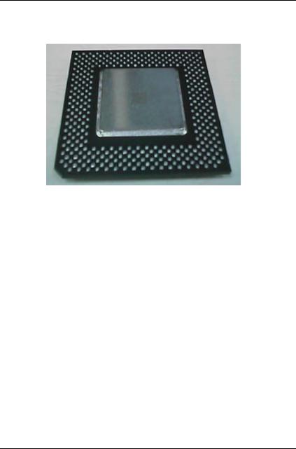
1.5. INTRODUCE THE INTELâCeleronTM Socket 370 Processor
Figure 1: INTELâ CeleronTM Socket370 Processor
1.6 What is AGP?
The Accelerated Graphics Port (AGP) is a new port on the Host-To-PCI bridge device that supports an AGP port. The main purpose of the AGP port is to provide fast access to system memory.
The AGP port can be used either as fast PCI port (32-bits at 66MHz vs. 32bits at 33MHz) or as an AGP port which supports 2x data-rate, a read queue, and side band addressing. When the 2x-data rate is used the port can transmit data at 533MB/sec (66.6*2*4). The read-queue can be used to pipeline reads – removing the effects of the reads-latency. Side band addressing can be used to transmit the data address on a separate line in order to speed up the transaction.
1-4
 Loading...