


FCC Compliance Statement:
This equipment has been tested and found to comply with limits for a Class B digital device , pursuant to Part 15 of the FCC rules. These limits are designed to provide reasonable protection against harmful interference in residential installations. This equipment generates, uses, and can radiate radio frequency energy, and if not installed and used in accordance with the instructions, may cause harmful interference to radio communications. However, there is no guarantee that interference will not occur in a particular installation. If this equipment does cause interference to radio or television equipment reception, which can be determined by turning the
equipment off and on, the user is encouraged to try to correct the interference by one or more of the following measures:
-Reorient or relocate the receiving antenna
-Move the equipment away from the receiver
-Plug the equipment into an outlet on a circuit different from that to which the receiver is connected
-Consult the dealer or an experienced radio/television technician for additional suggestions
You are cautioned that any change or modifications to the equipment not expressly approve by the party responsible for compliance could void Your authority to operate such equipment.
This device complies with Part 15 of the FCC Rules. Operation is subjected to the following two conditions 1) this device may not cause harmful interference and 2) this device must accept any interference received, including interference that may cause undesired operation.
Declaration of Conformity
We, Manufacturer/Importer
(full address)
G.B.T. Technology Träding GMbH
Ausschlager Weg 41, 1F, 20537 Hamburg, Germany
declare that the product
( description of the apparatus, system, installation to which it refers)
Mother Board
GA-6CMC7, GA-6CMC7R
is in conformity with
(reference to the specification under which conformity is declared) in accordance with 89/336 EEC-EMC Directive
|
EN 55011 |
Limits and methods of measurement |
|
|
of radio disturbance characteristics of |
|
|
industrial, scientific and medical (ISM |
|
|
high frequency equipment |
|
EN55013 |
Limits and methods of measurement |
|
|
of radio disturbance characteristics of |
|
|
broadcast receivers and associated |
|
|
equipment |
|
EN 55014 |
Limits and methods of measurement |
|
|
of radio disturbance characteristics of |
|
|
household electrical appliances, |
|
|
portable tools and similar electrical |
|
|
apparatus |
|
EN 55015 |
Limits and methods of measurement |
|
|
of radio disturbance characteristics of |
|
|
fluorescent lamps and luminaries |
|
EN 55020 |
Immunity from radio interference of |
|
|
broadcast receivers and associated |
|
|
equipment |
|
EN 55022 |
Limits and methods of measurement |
|
|
of radio disturbance characteristics of |
|
|
information technology equipment |
|
DIN VDE 0855 |
Cabled distribution systems; Equipment |
|
||
|
part 10 |
for receiving and/or distribution from |
|
part 12 |
sound and television signals |

 CE marking
EN 61000-3-2* |
Disturbances in supply systems caused |
EN60555-2 |
by household appliances and similar |
|
electrical equipment “Harmonics” |
EN61000-3-3* |
Disturbances in supply systems caused |
EN60555-3 |
by household appliances and similar |
|
electrical equipment “Voltage fluctuations” |
EN 50081-1 |
Generic emission standard Part 1: |
|
Residual, commercial and light industry |
EN 50082-1 |
Generic immunity standard Part 1: |
|
Residual, commercial and light industry |
EN 55081-2 |
Generic emission standard Part 2: |
|
Industrial environment |
EN 55082-2 |
Generic immunity standard Part 2: |
|
Industrial environment |
ENV 55104 |
Immunity requirements for household |
|
appliances tools and similar apparatus |
EN 50091- 2 |
EMC requirements for uninterruptible |
|
power systems (UPS) |
 (EC conformity marking)
The manufacturer also declares the conformity of above mentioned product with the actual required safety standards in accordance with LVD 73/23 EEC
EN 60065 |
Safety requirements for mains operated |
EN 60950 |
|
electronic and related apparatus for |
|
|
household and similar general use |
|
EN 60335 |
Safety of household and similar |
EN 50091-1 |
|
electrical appliances |
|
Manufacturer/Importer
Safety for information technology equipment including electrical business equipment
General and Safety requirements for uninterruptible power systems (UPS)
Signature : Rex Lin
(Stamp) |
Date : Mar. 24, 2000 |
Name : |
Rex Lin |
6CMC7 Series
Socket 370 Processor Motherboard
USER'S MANUAL
Socket 370 Processor Motherboard
REV. 1.1 Second Edition
R-11-02-000425

How this manual is organized
This manual is divided into the following sections:
1) |
Revision List |
Manual revision information |
|
|
|
2) |
Item Checklist |
Product item list |
|
|
|
3) Features |
Product information & specification |
|
|
|
|
4) |
Hardware Setup |
Instructions on setting up the motherboard |
|
|
|
5) Performance & Block Diagram |
Product performance & block diagram |
|
|
|
|
6) Suspend to RAM |
Instructions STR installation |
|
|
|
|
7) |
BIOS Setup |
Instructions on setting up the BIOS |
|
|
software |
|
|
|
8) |
Appendix |
General reference |
|
|
|

Table Of Content
Revision History |
P.1 |
|
|
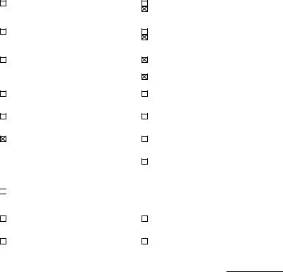
Item Checklist |
P.2 |
|
|
Summary of Features |
P.3 |
|
|
6CMC7/ 6CMC7R Motherboard Layout |
P.5 |
|
|
Page Index for CPU Speed Setup / Over Clock Jumper Setting / |
P.8 |
Connectors / Panel and Jumper Definition |
|
|
|
Performance List |
P.28 |
|
|
Block Diagram |
P.29 |
|
|
Suspend to RAM Installation |
P.30 |
|
|
Memory Installation |
P.43 |
|
|
Page Index for BIOS Setup |
P.44 |
|
|
Appendix |
P.77 |
|
|

6CMC7/ 6CMC7R Motherboard
Revision History
Revision |
Revision Note |
Date |
1.1 |
Initial release of the 6CMC7/ 6CMC7R motherboard |
Mar.200 |
|
user’s manual. |
0 |
1.1 |
Second release of the 6CMC7/6CMC7R motherboard |
Apr.2000 |
|
user’s manual. |
|
The author assumes no responsibility for any errors or omissions that may appear in this document nor does the author make a commitment to update the information contained herein. Third-party brands and names are the property of their respective owners.
Apr. 25, 2000 Taipei, Taiwan, R.O.C
1

Item Checklist
Item Checklist
þThe 6CMC7/ 6CMC7R Motherboard
þCable for IDE / Floppy device
þCD (IUCD) for motherboard utilities oInternal USB Cable (Optional)
þ6CMC7/ 6CMC7R User’s Manual
2

6CMC7/ 6CMC7R Motherboard
Summary of Features
Form factor |
Ÿ |
25 cm x 24.5 cm Micro ATX SIZE form factor, 4 layers PCB. |
CPU |
Ÿ |
Socket 370 processor |
|
|
Intel Pentiumâ !!! 100/133MHz FSB, Coppermine core FC-PGA |
|
|
Intel CeleronTM 100MHz FSB, Mendocimo core PPGA |
|
|
VIA Cyrix â III 133MHz FSB, PPGA (Optional) |
|
Ÿ 2nd cache in CPU (Depend on CPU) |
|
Chipset |
Ÿ |
82820 HOST / AGP / RDRAM Controller |
|
Ÿ 82801AA(ICH) I/O Controller Hub |
|
|
Ÿ 82805AA(MTH) Memory Translator Hub |
|
Clock Generator |
Ÿ |
Supports 100 / 133MHz |
|
|
110/120/140/150 MHz clocks (reserved) |
Memory |
Ÿ |
2 168-pin DIMM Sockets Support 2 banks. |
I/O Control |
Ÿ |
ITE IT8712 |
Slots |
Ÿ |
1 AMR (Audio Modem Riser) slot |
|
Ÿ 1 Universal AGP slot |
|
|
|
(1X / 2X / 4X 1.5V / 3.3V device support) |
|
Ÿ 3 32-bit Master PCI Bus slots(for 6CMC7) |
|
|
Ÿ 2 32-bit Master PCI Bus slots(for 6CMC7R) |
|
On-Board IDE |
Ÿ |
An IDE controller on the Intelâ 82801AA PCI chipset |
|
|
provides IDE HDD/ CD-ROM with PIO, Bus Master |
|
|
and Ultra DMA33/ATA66 operation modes |
|
Ÿ Can connect up to four IDE devices |
|
On-Board |
Ÿ |
1 Floppy port supports 2 FDD with 360K, 720K,1.2M, |
Peripherals |
|
1.44M and 2.88M bytes |
|
Ÿ 1 Parallel ports supports SPP/EPP/ECP mode |
|
|
Ÿ 2 Serial ports (COM A & COM B) |
|
|
Ÿ 2 USB ports (Front USB port optional) |
|
|
Ÿ |
1 IrDA connector |
|
Ÿ Smart Card Reader Connector |
|
Hardware Monitor |
Ÿ |
CPU/Power Supply/System Fan Revolution detect |
(Optional) |
Ÿ |
CPU Fan Control |
|
Ÿ |
System Voltage Detect |
|
Ÿ |
CPU Overheat Warning |
|
Ÿ |
Chassis Intrusion Detect |
|
Ÿ Display Actual Current Voltage |
|
|
|
To be continued… |
3

|
|
Summary of Features |
|
|
|
On-Board Sound |
Ÿ |
AC’97 |
|
Ÿ Line In / Line Out / Mic In / AUX In / CD In / TEL / |
|
|
|
Game Port |
PS/2 Connector |
Ÿ |
PS/2â Keyboard interface and PS/2â Mouse |
|
interface |
|
BIOS |
Ÿ |
Licensed AMI BIOS, 4M bit FWH |
On-Board LAN |
Ÿ |
Intelâ GD 82559(Optional) |
Additional Features |
Ÿ |
Internal/External Modem Wake up |
|
Ÿ STR (Suspend-To-RAM) |
|
|
Ÿ |
Wake On LAN |
|
Ÿ PS/2 Keyboard Password Wake up |
|
|
Ÿ PS/2 Mouse Wake up |
|
|
Ÿ System after AC back |
|
|
Ÿ Poly fuse for keyboard, USB, Game port overcurrent |
|
|
|
protection |
|
Ÿ USB KB/MS Wake Up from S3 |
|
4

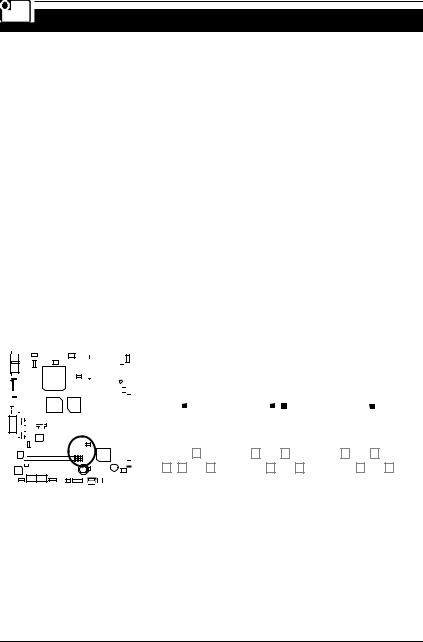
6CMC7/ 6CMC7R Motherboard
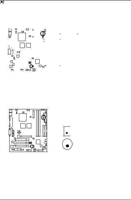
6CMC7/ 6CMC7R Motherboard Layout
PS/2 |
JP16 |
|
JP1 |
||
|
||
|
JP3 |
|
USB |
LAN |
|
|
COM A |
LPT
COM B |
|
|
|
AUDIO |
|
|
|
|
|
|
|
J7 |
|
|
|
|
|
|
|
|
|
|
|
|||
|
|
|
GAME & |
|
|
|
|
|
|
|
J8 |
|
|
|
|
|
|
|
JP24 |
|
|||||
|
|
|
|
|
|
|
||||||
|
|
|
|
|
|
|
|
|
|
|
|
|
PGA 370
CPU
|
|
|
|
|
|
|
|
|
|
MCH |
|
|
|
|
|
|
|
82820 |
|||
|
|
|
|
|
|
|
J19 |
|||
|
|
|
|
|
|
|
||||
|
|
|
|
|
|
|
|
|
J6 |
|
|
Intel |
|
|
|
AGP 1 |
|||||
|
|
|
|
|||||||
82559 |
|
|
|
|
||||||
PCI 1 |
|
|
|
|
||||||
AC97 |
|
|
|
|
|
|
|
JP26 |
|||||||||||
|
|
|
|
|
|
JP9 |
|
|
PCI 2 |
||||||||||
BIOS |
JP10 |
PCI 3 |
|||||||||||||||||
|
|
|
|
|
|
|
|
|
|
|
|
|
|
|
|
|
|
|
|
JP11 |
|
|
|
|
|
|
|
|
|
|
AMR 1 |
|
|
|
|
|
J2 |
||
|
|
J22 |
|
J1 |
|
|
J17 |
|
POWER |
J14 |
|
JP18 |
ATX |
JP15 |
|
|
|
FDD1 |
|
|
|
LED1 |
|
|
|
JP29 |
|
|
|
|
J15 |
MTH
82805
|
|
IDE2 |
IDE1 |
|
|
6CMC7 |
1 |
2 |
|
|
|
DIMM |
DIMM |
|
|
||
|
|
|
|||
JP8 |
|
JP20 |
J20 |
|
|
|
|
|
|
||
|
|
ICH |
J16 |
|
|
SW1 |
|
JP17 |
JP6 |
||
82801 |
|||||
|
|
|
|||
|
|
|
JP5 |
|
|
BAT1 |
|
BZ 1 |
|
|
|
|
|
JP14 |
|
||
|
|
|
|
||
|
|
|
JP27 |
|
J12 |
J10 |
JP22 |
JP28 |
JP4 |
J11 |
J21 |
|
|
|
|
J23 |
|
|
|
JP21 |
|
|
|
|
|
|
|
|
5

6CMC7/ 6CMC7R Motherboard Layout
$ |
|
|
Page Index for CPU Speed Setup/ Over Clock Jumper Setting / |
Page |
|
Connectors / Panel and Jumper Definition |
|
|
CPU Speed Setup |
P.8 |
|
Over Clock Jumper Setting |
P.9 |
|
JP20 (SDRAM Over Clock) [Optional] |
P.9 |
|
JP29 (Over Clock Voltage for SDRAM) [Optional] |
P.10 |
|
J22 |
(Over Voltage CPU Speed Up) [Optional] |
P.10 |
Connectors |
P.11 |
|
GAME & Audio Port |
P.11 |
|
COM A / COM B / LPT Port |
P.11 |
|
USB & LAN Connector |
P.12 |
|
PS/2 Keyboard & PS/2 Mouse Connector |
P.12 |
|
J1 (CPU FAN) |
P.13 |
|
J17 |
(Power FAN) |
P.13 |
J16 |
(System FAN) |
P.14 |
ATX Power |
P.14 |
|
Floppy Port |
P.15 |
|
IDE (Primary/ Secondary) Port |
P.15 |
|
IR |
|
P.16 |
JP15 (STR LED Connector & DIMM LED) |
P.16 |
|
J8 (AUX_IN) |
P.17 |
|
J6 (CD Audio Line In) |
P.17 |
|
J7 (TEL) |
P.18 |
|
J2 (Wake On LAN) |
P.18 |
|
J10 |
(Ring Power On) |
P.19 |
J15 |
(External SMBUS Device Connector) |
P.19 |
JP22 (Front Panel USB Port) |
P.20 |
|
J19 (Audio PIN) |
P.20 |
|
J20 (CD/IN PIN) |
P.21 |
|
J12 |
(Smart Card Reader) |
P.21 |
Panel and Jumper Definition |
P.22 |
|
J23 (2x11 pins jumper) [for 6CMC7] |
P.22 |
|
J11 |
(Panel Jumper) [for 6CMC7R] |
P.23 |
|
|
|
6

6CMC7/ 6CMC7R Motherboard
JP27& JP28 (USB Port Selection) [Optional] |
P.23 |
JP16 (PS/2 Keyboard Power On) |
P.24 |
JP18 (STR Selection) |
P.24 |
JP17(Case Open) |
P.25 |
7

6CMC7/ 6CMC7R Motherboard Layout |
|
|
|
JP6 (Timeout Reboot Function) |
P.25 |
JP5 (Safe mode/Recovery/Normal) |
P.26 |
JP4 (Clear CMOS Function) |
P.26 |
JP9 (Top Block Lock) |
P.27 |
JP10 (FWH Write Protection) [Optional] |
P.27 |
JP14 (Buzzer Enable) [Optional] |
P.28 |
JP11 (AMR Select) |
P.28 |
JP24 (Onboard LAN Function) [Optional] |
P.29 |
JP1 (Cyrix CPU Turbo Function) [Optional] |
P.29 |
JP26 (PME Function) [Optional] |
P.30 |
JP21 (Front USB Device Wake Up Selection) [Optional] |
P.30 |
JP3 (USB Device Wake Up Selection) |
P.31 |
J21 (SPK) [Optional] |
P.31 |
Bat 1 (Battery) |
P.32 |
8
CPU Speed Setup
CPU Speed Setup
The system bus frequency can be switched at 100MHz ,133MHz and Auto by adjusting JP8 & SW1. The CPU Frequency is control by BIOS.
JP8 / SW1 Select the System Speed at 100MHz , 133MHz and Auto.
|
CPU |
|
|
|
|
|
|
|
|
|
|
|
|
|
|
|
|
SW1 |
|
|
|
|
|
|
|
|
|
|
JP8 |
|
AGP |
|
|
|
|
|
|
|
|
|
|
|||||||||||
|
CLK |
1 |
|
|
|
|
2 |
|
|
|
3 |
|
4 |
|
|
|
|
|
|
CLK |
|
|
|
|
|
|
|
|
|
|
||||||||||||||||||||||
|
|
|
|
|
|
|
|
|
|
|
|
|
|
|
|
|
|
|
|
|
|
|
|
|
|
|
||||||||||||||||||||||||||
|
|
|
|
|
|
|
|
|
|
|
|
|
|
|
|
|
|
|
|
|
|
|
|
|
|
|
|
|
|
|
|
|
|
|
|
|
||||||||||||||||
|
|
|
|
|
|
|
|
|
|
|
|
|
|
|
|
|
|
|
|
|
|
|
|
|
|
|
|
|
|
|
|
|
|
|
|
|
|
|
|
|
|
|
|
|
|
|
|
|
|
|
|
|
100 |
|
|
|
|
|
|
O |
|
|
O |
|
|
|
X |
|
|
|
O |
|
|
OFF |
|
66.6 |
|
|
|
|
|
|
|
|
|
|
|
||||||||||||||||||
105 |
|
|
|
|
|
|
O |
|
|
O |
|
|
|
O |
|
|
|
O |
|
|
OFF |
|
70 |
|
|
|
|
|
|
|
|
|
|
|
||||||||||||||||||
110 |
|
|
|
|
|
|
O |
|
|
|
X |
|
|
|
O |
|
|
|
O |
|
|
OFF |
|
73.3 |
|
|
|
|
|
|
|
|
|
|
|
|||||||||||||||||
115 |
|
|
|
|
|
|
O |
|
|
|
X |
|
|
|
O |
|
|
|
X |
|
|
OFF |
|
76.6 |
|
|
|
|
|
|
|
|
|
|
|
|||||||||||||||||
120 |
|
|
|
|
|
|
O |
|
|
|
X |
|
|
|
X |
|
|
|
X |
|
|
OFF |
|
80.0 |
|
|
|
|
|
|
|
|
|
|
|
|||||||||||||||||
125 |
|
|
|
|
|
|
X |
|
|
O |
|
|
|
O |
|
|
|
O |
|
|
OFF |
|
83.3 |
|
|
|
|
|
|
|
|
|
|
|
||||||||||||||||||
133 |
|
|
|
|
|
|
X |
|
|
O |
|
|
|
X |
|
|
|
O |
|
|
OFF |
|
66.6 |
|
|
|
|
|
|
|
|
|
|
|
||||||||||||||||||
140 |
|
|
|
|
|
|
X |
|
|
|
X |
|
|
|
O |
|
|
|
X |
|
|
OFF |
|
70.0 |
|
|
|
|
|
|
|
|
|
|
|
|||||||||||||||||
150 |
|
|
|
|
|
|
X |
|
|
|
X |
|
|
|
X |
|
|
|
X |
|
|
OFF |
|
75.0 |
|
|
|
|
|
|
|
|
|
|
|
|||||||||||||||||
|
Auto |
|
|
X |
|
|
O |
|
|
|
X |
|
|
|
O |
|
|
ON |
|
66.6 |
|
|
|
|
|
|
|
|
|
|
|
|||||||||||||||||||||
(O: ON / X : OFF) |
|
|
|
|
|
|
|
|
|
|
|
|
|
|
|
|
|
|
|
|
|
|
|
|
|
|
|
|
|
|
|
|
|
|
|
|
||||||||||||||||
|
|
|
|
|
|
|
|
|
|
|
|
|
|
|
|
|
|
|
|
|
|
|
|
|
|
|
100MHz |
|
|
133MHz |
100/133MHz |
|||||||||||||||||||||
|
|
|
|
|
|
|
|
|
|
|
|
|
|
|
|
|
|
|
|
|
|
|
|
|
|
|
|
|
JP8 |
|
|
|
JP8 |
|
Auto |
|||||||||||||||||
|
|
|
|
|
|
|
|
|
|
|
|
|
|
|
|
|
|
|
|
|
|
|
|
|
|
|
|
|
|
|
|
|
||||||||||||||||||||
|
|
|
|
|
|
|
|
|
|
|
|
|
|
|
|
|
|
|
|
|
|
|
|
|
|
|
|
|
|
|
|
|
||||||||||||||||||||
|
|
|
|
|
|
|
|
|
|
|
|
|
|
|
|
|
|
|
|
|
|
|
|
|
|
1 |
1 |
|
JP8 |
|||||||||||||||||||||||
|
|
|
|
|
|
|
|
|
|
|
|
|
|
|
|
|
|
|
|
|
|
|
|
|
|
|
|
|
|
|
|
|
|
|
|
|
|
|
1 |
|
|
|
|
|
|
|||||||
|
|
|
|
|
|
|
|
|
|
|
|
|
|
|
|
|
|
|
|
|
|
|
|
|
|
|
|
|
|
|
|
|
|
|
|
|
|
|
|
|
|
|
|
|
||||||||
|
|
|
|
|
|
|
|
|
|
|
|
|
|
|
|
|
|
|
|
|
|
|
|
|
|
|
|
|
|
|
|
|
|
|
|
|
||||||||||||||||
|
|
|
|
|
|
|
|
|
|
|
|
|
|
|
|
|
|
|
|
|
|
|
|
|
|
ON |
|
ON |
|
ON |
||||||||||||||||||||||
|
|
|
|
|
|
|
|
|
|
|
|
|
|
|
|
|
|
|
|
|
|
|
|
|
|
|
|
|||||||||||||||||||||||||
|
|
|
|
|
|
|
|
|
|
|
|
|
|
|
|
|
|
|
|
|
|
|
|
|
|
|
|
|
|
|
|
|
|
|
|
|
|
|
|
|
|
|
|
|
|
|
|
|
||||
|
|
|
|
|
|
|
|
|
|
|
|
|
|
|
|
|
|
|
|
|
|
|
|
|
|
|
1 |
|
2 |
3 |
|
4 |
|
|
1 |
2 |
3 |
|
4 |
|
|
1 |
2 |
3 |
4 |
|
|
|||||
|
|
|
|
|
|
|
|
|
|
|
|
|
|
|
|
|
|
|
|
|
|
|
|
|
|
|
|
|
|
|
|
|
|
|
|
|||||||||||||||||
|
|
|
|
|
|
|
|
|
|
|
|
|
|
|
|
|
|
|
|
|
|
|
|
|
|
|
|
|
|
|
|
|
|
|
|
|||||||||||||||||
|
|
|
|
|
|
|
|
|
|
|
|
|
|
|
|
|
|
|
|
|
|
|
|
|
|
|
|
|
|
|
|
|
|
|
|
|||||||||||||||||
|
|
|
|
|
|
|
|
|
|
|
|
|
|
|
|
|
|
|
|
|
|
|
|
|
|
|
|
|
|
|
|
|
|
|
|
|||||||||||||||||
|
|
|
|
|
|
|
|
|
|
|
|
|
|
|
|
|
|
|
|
|
|
|
|
|
|
|
|
|
|
|
|
|||||||||||||||||||||
|
|
|
|
|
|
|
|
|
|
|
|
|
|
|
|
|
|
|
|
|
|
|
|
|
|
|
|
SW1 |
|
|
|
|
SW1 |
|
|
SW1 |
|
|||||||||||||||
MJP8 Open : Force 100MHz
Close : Auto
9
6CMC7/ 6CMC7R Motherboard
Over Clock Jumper Setting
(We don’t guaranteed over clock jumper to work àJP20,JP29,J22)
JP20: SDRAM Over Clock (Optional)
1


|
|
|
|
|
|
|
|
|
|
|
|
|
|
|
|
|
|
|
|
|
|
|
|
Pin No. |
Definition |
|
|
|
|
|
|
|
|
|
|
|
|
|
|
|
|
|
|
|
|
|
|
|
|
||
|
|
|
|
|
|
|
|
|
|
|
|
|
|
|
|
|
|
|
|
|
|
|
|
||
|
|
|
|
|
|
|
|
|
|
|
|
|
|
|
|
|
|
|
|
|
|
|
|
Open |
Turbo |
|
|
|
|
|
|
|
|
|
|
|
|
|
|
|
|
|
|
|
|
|
|
|
|
Close |
Normal (Default) |
|
|
|
|
|
|
|
|
|
|
|
|
|
|
|
|
|
|
|
|
|
|
|
|
||
|
|
|
|
|
|
|
|
|
|
|
|
|
|
|
|
|
|
|
|
|
|
|
|
||
|
|
|
|
|
|
|
|
|
|
|
|
|
|
|
|
|
|
|
|
|
|
|
|
|
|
|
|
|
|
|
|
|
|
|
|
|
|
|
|
|
|
|
|
|
|
|
|
|
|
|
|
|
|
|
|
|
|
|
|
|
|
|
|
|
|
|
|
|
|
|
|
|
|
|
|
|
|
|
|
|
|
|
|
|
|
|
|
|
|
|
|
|
|
|
|
|
|
|
|
|
|
|
|
|
|
|
|
|
|
|
|
|
|
|
|
|
|
|
|
|
|
|
|
|
|
|
|
|
|
|
|
|
|
|
|
|
|
|
|
|
|
|
|
|
|
|
|
|
|
|
|
|
|
|
|
|
|
|
|
|
|
|
|
|
|
|
|
|
|
|
|
|
|
|
|
|
|
|
|
|
|
|
|
|
|
|
|
|
|
|
|
|
|
|
|
|
|
|
|
|
|
|
|
|
|
|
|
|
|
|
|
|
|
|
|
|
|
|
|
|
|
|
|
|
|
|
|
|
|
|
|
|
|
|
|
|
|
|
|
|
|
|
|
|
|
|
|
|
|
|
|
|
|
|
|
|
|
|
|
|
|
|
|
|
|
|
|
|
|
|
|
|
|
|
|
|
|
|
|
|
|
|
|
|
|
|
|
|
|
|
|
|
|
|
|
|
|
|
|
|
|
|
|
|
|
|
|
|
|
|
|
|
|
|
|
|
|
|
|
|
|
|
|
|
|
|
|
|
|
|
|
|
|
|
|
|
|
|
|
|
|
|
|
|
|
|
|
|
|
|
|
|
|
|
|
|
|
|
|
|
|
|
|
|
|
|
|
|
|
|
|
|
Close : Normal (Default) |
Open : Turbo |
|||||||||||||||||||||||
|
|
|
|
|
|
|
|
|
|
|
|
|
|
|
|
|
|
|||||||||||||
|
|
|
|
|
CPU CLK |
|
|
|
|
|
DRAM CLK |
CPU CLK |
DRAM CLK |
|||||||||||||||||
|
|
|
100 |
|
|
|
|
|
|
|
100 |
100 |
100 |
|||||||||||||||||
|
|
|
* 105 |
|
|
|
|
|
|
105 |
* 105 |
105 |
||||||||||||||||||
|
|
|
* 110 |
|
|
|
|
|
|
110 |
* 110 |
110 |
||||||||||||||||||
|
|
|
* 115 |
|
|
|
|
|
|
115 |
* 115 |
115 |
||||||||||||||||||
|
|
|
* 120 |
|
|
|
|
|
|
120 |
* 120 |
120 |
||||||||||||||||||
|
|
|
* 125 |
|
|
|
|
|
|
94 |
* 125 |
125 |
||||||||||||||||||
|
|
|
133 |
|
|
|
|
|
|
|
100 |
* 133 |
133 |
|||||||||||||||||
|
|
|
* 140 |
|
|
|
|
|
|
105 |
* 140 |
140 |
||||||||||||||||||
|
|
|
* 150 |
|
|
|
|
|
|
112 |
* 150 |
150 |
||||||||||||||||||
|
|
|
|
|
|
|
|
|
|
|
|
|
|
|
|
|
|
|
|
|
|
|
|
|
|
|
|
|
|
|
If instability should occur to your system, please adjust JP29.
(* this setting are not guaranteed)
10
6CMC7/ 6CMC7R Motherboard
JP29 : Over Clock Voltage for SDRAM (Optional)
|
|
|
|
|
|
|
|
|
|
|
|
|
|
|
|
|
|
|
|
|
|
|
|
1 |
|
|
|
|
|
|
|
|
|
|
|
|
|
|
|
|
|
|
|
|
|
|
|
|
|
|
|
|
|
|
|
|
|
|
|
|
|
|
|
|
|
|
|
|
|
|
|
|
|
|
|
|
|
|
|
|
|
|
|
|
|
|
|
|
|
|
|
|
|
|
|
|
|
|
|
|
|
|
|
|
|
|
|
|
|
|
|
|
|
|
|
|
|
|
|
|
|
|
|
|
|
|
|
|
|
|
|
|
|
|
|
|
|
|
|
|
|
|
|
|
|
|
|
|
|
|
|
|
|
|
|
|
|
|
|
|
|
|
|
|
|
|
|
|
|
|
|
|
|
|
|
|
|
|
|
|
|
|
|
|
|
|
|
|
|
|
|
|
|
|
|
|
|
|
|
|
|
|
|
|
|
|
|
|
|
|
|
|
|
|
|
|
|
|
|
|
|
|
|
|
|
|
|
|
|
|
|
|
|
|
|
|
|
|
|
|
|
|
|
|
|
|
|
|
|
|
|
|
|
|
Pin No. |
|
|
|
Definition |
|
|
|
|
|
|
|
|
|
|
|
|
|
|
|
|
|
|
|
|
|
|
|
|
1-2close |
Over Clock |
||||
|
|
|
|
|
|
|
|
|
|
|
|
|
|
|
|
|
|
|
|
|
|
|
||||||
|
|
|
|
|
|
|
|
|
|
|
|
|
|
|
|
|
|
|
|
|
|
|
2-3close |
Normal (Default) |
||||
|
|
|
|
|
|
|
|
|
|
|
|
|
|
|
|
|
|
|
|
|
|
|
||||||
J22 : Over Voltage CPU Speed Up (Optional)(Magic Booster)
|
|
Pin No. |
Definition |
|
|
1-2 |
Normal |
2 |
12 |
close |
(Default) |
|
|
3-4 |
10% |
|
|
close |
|
1 |
11 |
|
|
5-6 |
20% |
||
|
|
close |
|
|
|
|
|
|
|
7-8 |
30% |
|
|
close |
|
|
|
|
|
|
|
9-10 |
40% |
|
|
close |
|
|
|
|
|
|
|
11-12 |
50% |
|
|
close |
|
|
|
|
11
6CMC7/ 6CMC7R Motherboard
Connectors
GAME & Audio Port


 GAME
GAME
Port
|
|
|
|
|
|
|
|
|
|
|
|
|
|
|
|
|
|
|
|
|
|
|
|
|
|
|
|
|
|
|
|
|
|
|
|
|
|
|
|
|
|
|
|
|
|
|
|
|
|
|
|
|
|
|
|
|
|
|
|
|
|
|
|
|
|
|
|
|
|
|
Line Out |
MIC |
|||
|
|
|
|
|
|
|
|
|
|
|
|
|
|
|||||
|
|
|
||||||||||||||||
Line In
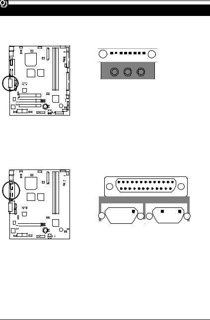
COM A / COM B / LPT Port
LPT Port
|
|
|
|
|
|
|
|
|
|
|
|
|
|
|
|
|
|
|
|
|
|
|
|
|
|
|
|
|
|
|
|
|
|
|
|
|
|
|
|
|
|
|
|
|
|
|
|
|
|
|
|
|
|
|
|
|
|
|
|
|
|
|
|
|
|
|
|
|
|
|
|
|
|
|
|
|
|
|
|
|
|
|
|
|
|
|
|
|
|
|
|
|
|
|
|
|
|
|
|
|
|
|
|
|
|
|
|
|
|
|
|
|
|
|
|
|
|
|
|
|
|
|
|
|
|
|
|
|
|
|
|
|
|
|
|
|
|
|
|
|
|
|
|
|
|
|
|
|
|
|
|
|
|
|
|
|
|
|
|
|
|
|
|
|
|
|
|
|
|
|
|
|
|
|
|
|
|
|
|
|
|
|
|
|
|
|
|
|
|
|
|
|
|
|
|
|
|
|
|
|
|
|
|
|
|
|
|
|
|
|
|
|
|
|
|
|
|
|
|
|
|
|
|
|
|
|
|
|
|
|
|
|
|
|
|
|
|
|
|
|
|
|
|
|
|
|
|
|
|
|
|
|
|
|
|
|
|
|
|
|
|
|
|
|
|
|
|
|
|
|
|
|
|
|
|
|
|
|
|
|
|
|
|
|
|
|
|
|
|
|
|
|
|
|
|
|
|
|
|
|
|
|
|
|
|
|
|
|
|
|
|
|
|
|
|
|
|
|
|
|
|
|
|
|
|
|
|
|
|
|
|
|
|
|
|
|
|
|
|
|
|
|
|
|
|
|
|
|
|
|
|
|
|
|
|
|
|
|
|
|
|
|
|
|
|
|
|
|
|
|
|
|
|
|
|
|
|
|
|
|
|
|
|
|
|
|
|
|
|
|
|
|
|
|
|
|
|
|
|
|
|
|
|
|
|
|
|
|
|
|
|
|
|
|
|
|
|
|
|
|
|
|
|
|
|
|
|
|
|
|
|
|
|
|
|
|
|
|
|
|
|
|
|
|
|
|
|
|
|
|
|
|
|
|
|
|
|
|
|
|
|
|
|
|
|
|
|
|
|
|
|
|
|
|
|
|
|
|
|
|
|
|
|
|
|
|
|
|
|
|
|
|
|
|
|
|
|
|
|
|
|
|
|
|
|
|
|
|
|
|
|
|
|
|
|
|
|
|
|
|
|
|
|
|
|
|
|
|
|
|
|
|
|
|
|
|
|
|
|
|
|
|
|
|
|
|
|
|
|
|
|
|
|
|
|
|
|
|
|
|
|
|
|
|
|
|
|
|
|
|
|
|
|
|
|
|
|
|
|
|
|
|
|
|
|
|
|
|
|
|
|
|
|
|
|
|
|
|
|
|
|
|
|
|
|
|
|
|
|
|
|
|
|
|
|
|
|
|
|
|
|
|
|
|
|
|
|
|
|
COM A |
|
COM B |
|||||||||||||||||||||||||||
|
|
|
|
|
|
|
|
|
|
|
|
|
|
|
|
|
|
|
|
|
|
|
|
|
|
|
|
|
|
|
|
|
|
|
|
|
|
|
|
|
|
|
|
|
|
|
|
|
|
|
|
|
|
|
|
|
|
|
|
|
|
|
|
|
|
|
|
|
|
|
|
|
|
|
|
|
|
|
|
|
|
|
|
|
|
|
|
|
|
|
|
|
|
|
|
|
|
|
|
|
|
|
|
|
|
|
|
|
|
|
|
|
|
|
|
|
|
|
|
|
|
|
|
|
|
|
|
|
|
|
|
12
6CMC7/ 6CMC7R Motherboard
USB & LAN : USB & LAN Connector
|
1 |
|
2 |
5 |
8 |
6 |
7 |
1 2 3 4
1 – Green LED
(LAN Link LED)
2 – Yellow LED
(LAN Active LED)
Pin No. Definition
1USB V0
2USB D0-
3USB D0+
4GND
5USB V1
6USB D1-
7USB D1+
8GND
PS/2 Keyboard & PS/2 Mouse Connector
PS/2 Mouse |
PS/2 Mouse/ Keyboard |
||
|
|
||
|
|
Pin No. |
Definition |
6 |
5 |
1 |
Data |
2 |
NC |
||
4 |
3 |
3 |
GND |
|
|
4 |
VCC(+5V) |
2 |
1 |
5 |
Clock |
PS/2 Keyboard |
6 |
NC |
|
13
Connectors
J1 : CPU FAN
1 


|
|
|
|
|
|
|
|
|
|
|
|
|
|
|
|
|
|
|
|
|
|
|
|
|
|
|
|
|
|
|
|
|
|
|
|
|
|
|
|
|
|
|
|
|
|
|
|
|
|
|
|
|
|
|
|
|
|
|
|
|
|
|
|
|
|
|
|
|
|
|
|
|
|
Pin No. |
Definition |
|
|
|
|
|
|
|
|
|
|
|
|
|
|
|
|
|
|
|
|
|
|
|
|
|
|
|
|
|
|
|
|
|
|
|
|
||
|
|
|
|
|
|
|
|
|
|
|
|
|
|
|
|
|
|
|
|
|
|
|
|
|
|
|
|
|
|
|
|
|
|
|
|
1 |
Control |
|
|
|
|
|
|
|
|
|
|
|
|
|
|
|
|
|
|
|
|
|
|
|
|
|
|
|
|
|
|
|
|
|
|
|
|
||
|
|
|
|
|
|
|
|
|
|
|
|
|
|
|
|
|
|
|
|
|
|
|
|
|
|
|
|
|
|
|
|
|
|
|
|
2 |
+12V |
|
|
|
|
|
|
|
|
|
|
|
|
|
|
|
|
|
|
|
|
|
|
|
|
|
|
|
|
|
|
|
|
|
|
|
|
3 |
SENSE |
|
|
|
|
|
|
|
|
|
|
|
|
|
|
|
|
|
|
|
|
|
|
|
|
|
|
|
|
|
|
|
|
|
|
|
|
||
|
|
|
|
|
|
|
|
|
|
|
|
|
|
|
|
|
|
|
|
|
|
|
|
|
|
|
|
|
|
|
|
|
|
|
|
||
|
|
|
|
|
|
|
|
|
|
|
|
|
|
|
|
|
|
|
|
|
|
|
|
|
|
|
|
|
|
|
|
|
|
|
|
|
|
J17 : Power FAN
|
|
|
|
|
|
|
|
|
|
|
|
|
|
|
|
|
|
|
|
|
|
|
|
|
|
|
|
|
|
|
|
|
|
|
|
|
1 |
|
|
|
|
|
|
|
|
|
|
|
|
|
|
|
|
|
|
|
|
|
|
|
|
|
|
|
|
|
|
|
|
|
|
|
|
|
|
|
|
|
|
|
|
|
|
|
|
|
|
|
|
|
|
|
|
|
|
|
|
|
|
|
|
|
|
|
|
|
|
|
|
|
|
|
|
|
|
|
|
|
|
|
|
|
|
|
|
|
|
|
|
|
|
|
|
|
|
|
|
|
|
|
|
|
|
|
|
|
|
|
|
|
|
|
|
|
|
|
|
|
|
|
|
|
|
|
|
|
|
|
|
|
|
|
|
|
|
|
|
|
|
|
|
|
Pin No. |
|
Definition |
||||
|
|
|
|
|
|
|
|
|
|
|
|
|
|
|
|
|
|
|
|
|
|
|
|
|
|
|
|
|
|
|
1 |
|
|
|
|
|
Control |
|
|
|
|
|
|
|
|
|
|
|
|
|
|
|
|
|
|
|
|
|
|
|
|
|
|
|
|
|
|
|
|
|
|
|
|
|
|
|
|
|
|
|
|
|
|
|
|
|
|
|
|
|
|
|
|
|
|
|
|
|
|
|
|
|
|
|
|
|
2 |
|
|
|
|
|
+12V |
|
|
|
|
|
|
|
|
|
|
|
|
|
|
|
|
|
|
|
|
|
|
|
|
|
|
|
|
|
|
|
3 |
|
|
|
|
|
SENSE |
|
|
|
|
|
|
|
|
|
|
|
|
|
|
|
|
|
|
|
|
|
|
|
|
|
|
|
|
|
|
|
|
|
|
|
|
||
|
|
|
|
|
|
|
|
|
|
|
|
|
|
|
|
|
|
|
|
|
|
|
|
|
|
|
|
|
|
|
|
|
|
|
|
||
14
6CMC7/ 6CMC7R Motherboard
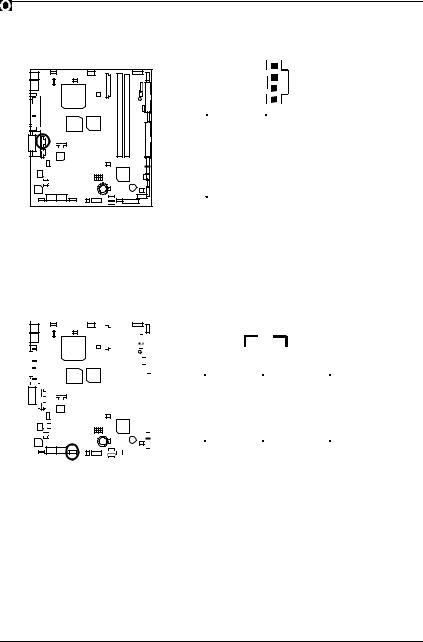
J16 : System FAN
1 |
|
|
|
|
|
|
|
|
|
|
|
|
|
|
|
|
|
|
|
|
|
|
|
|
|
|
|
|
|
|
|
|
|
|
|
|
|
Pin No. |
Definition |
|
|
|
|
|
|
|
|
|
|
|
|
|
|
|
|
|
|
|
|
|
|
|
|
|
|
|
|
|
|
|
|
|
|
|
|
|
||
|
|
|
|
|
|
|
|
|
|
|
|
|
|
|
|
|
|
|
|
|
|
|
|
|
|
|
|
|
|
|
|
|
|
|
|
|
||
|
|
|
|
|
|
|
|
|
|
|
|
|
|
|
|
|
|
|
|
|
|
|
|
|
|
|
|
|
|
|
|
|
|
|
|
|
1 |
Control |
|
|
|
|
|
|
|
|
|
|
|
|
|
|
|
|
|
|
|
|
|
|
|
|
|
|
|
|
|
|
|
|
|
|
|
|
|
2 |
+12V |
|
|
|
|
|
|
|
|
|
|
|
|
|
|
|
|
|
|
|
|
|
|
|
|
|
|
|
|
|
|
|
|
|
|
|
|
|
||
|
|
|
|
|
|
|
|
|
|
|
|
|
|
|
|
|
|
|
|
|
|
|
|
|
|
|
|
|
|
|
|
|
|
|
|
|
3 |
SENSE |
|
|
|
|
|
|
|
|
|
|
|
|
|
|
|
|
|
|
|
|
|
|
|
|
|
|
|
|
|
|
|
|
|
|
|
|
|
ATX Power
|
|
|
|
|
|
|
|
|
|
|
|
|
|
|
|
|
|
|
|
|
|
|
|
|
|
|
|
|
|
|
|
|
|
|
|
|
|
|
|
|
|
|
|
|
|
|
|
|
|
|
|
|
|
|
|
|
|
Pin No. |
Definition |
|
|
|
|
|
|
|
|
|
|
|
|
|
|
|
|
|
|
|
|
|
|
|
|
|
|
10 20 |
|
||
|
|
|
|
|
|
|
|
|
|
|
|
|
|
|
|
|
|
|
|
|
|
|
|
|
|
|
|
3,5,7,13,15-17 |
GND |
|
|
|
|
|
|
|
|
|
|
|
|
|
|
|
|
|
|
|
|
|
|
|
|
|
|
|
|
||
|
|
|
|
|
|
|
|
|
|
|
|
|
|
|
|
|
|
|
|
|
|
|
|
|
|
|
|
1,2,11 |
3.3V |
|
|
|
|
|
|
|
|
|
|
|
|
|
|
|
|
|
|
|
|
|
|
|
|
|
|
|
|
4,6,19,20 |
VCC |
|
|
|
|
|
|
|
|
|
|
|
|
|
|
|
|
|
|
|
|
|
|
|
|
|
|
|
|
10 |
+12V |
|
|
|
|
|
|
|
|
|
|
|
|
|
|
|
|
|
|
|
|
|
|
|
|
|
|
|
|
12 |
-12V |
|
|
|
|
|
|
|
|
|
|
|
|
|
|
|
|
|
|
|
|
|
|
|
|
|
|
|
|
18 |
-5V |
|
|
|
|
|
|
|
|
|
|
|
|
|
|
|
|
|
|
|
|
|
|
|
|
|
|
|
|
||
|
|
|
|
|
|
|
|
|
|
|
|
|
|
|
|
|
|
|
|
|
|
|
|
|
|
1 11 |
|
8 |
Power Good |
|
|
|
|
|
|
|
|
|
|
|
|
|
|
|
|
|
|
|
|
|
|
|
|
|
|
|
|||
|
|
|
|
|
|
|
|
|
|
|
|
|
|
|
|
|
|
|
|
|
|
|
|
|
|
|
|
9 |
5V SB stand by+5V |
|
|
|
|
|
|
|
|
|
|
|
|
|
|
|
|
|
|
|
|
|
|
|
|
|
|
|
|
14 |
PS-ON(Soft On/Off) |
|
|
|
|
|
|
|
|
|
|
|
|
|
|
|
|
|
|
|
|
|
|
|
|
|
|
|
|
15
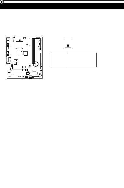
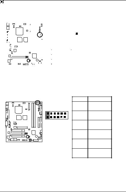
Connectors
Floppy Port
 RED LINE
IDE1(Primary) , IDE2 (Secondary) Port
RED LINE
IDE 2 IDE 1
16
6CMC7/ 6CMC7R Motherboard
IR
|
|
|
|
|
|
|
|
|
|
|
|
|
|
|
|
|
|
|
|
|
|
|
|
|
|
|
|
|
|
|
|
|
|
|
|
|
|
|
|
|
|
|
|
|
|
|
|
|
|
|
|
|
|
|
|
|
|
|
|
|
|
|
|
|
|
|
|
|
|
|
|
|
|
|
|
|
|
|
|
|
|
|
|
|
|
|
|
|
|
|
|
|
|
|
|
|
|
|
|
|
|
|
|
1 |
|
|
|
|
PIN No. |
Definition |
|
|
|
|
|||||||||||||||||||||||||||||||||
|
|
|
|
|
|
|
|
|
|
|
|
|
|
|
|
|
|
|
|
|
|
|
|
|
|
|
|
|
|
|
|
|
|
|
1 |
VCC(+5V) |
|
|
|
|
|
|
|
|
|
|
|
|
|
|
|
|
|
|
|
|
|
|
|
|
|
|
|
|
|
|
|
|
|
|
|
||
|
|
|
|
|
|
|
|
|
|
|
|
|
|
|
|
|
|
|
|
|
|
|
|
|
|
|
|
|
|
|
|
|
|
|
2 |
NC |
|
|
|
|
|
|
|
|
|
|
|
|
|
|
|
|
|
|
|
|
|
|
|
|
|
|
|
|
|
|
|
|
|
|
|
3 |
IR data input |
|
|
|
|
|
|
|
|
|
|
|
|
|
|
|
|
|
|
|
|
|
|
|
|
|
|
|
|
|
|
|
|
|
|
|
||
|
|
|
|
|
|
|
|
|
|
|
|
|
|
|
|
|
|
|
|
|
|
|
|
|
|
|
|
|
|
|
|
|
|
|
4 |
GND |
|
|
|
|
|
|
|
|
|
|
|
|
|
|
|
|
|
|
|
|
|
|
|
|
|
|
|
|
|
|
|
|
|
|
|
||
|
|
|
|
|
|
|
|
|
|
|
|
|
|
|
|
|
|
|
|
|
|
|
|
|
|
|
|
|
|
|
|
|
|
|
5 |
IR data output |
|
|
|
|
|
|
|
|
|
|
|
|
|
|
|
|
|
|
|
|
|
|
|
|
|
|
|
|
|
|
|
|
|
|
|
||
|
|
|
|
|
|
|
|
|
|
|
|
|
|
|
|
|
|
|
|
|
|
|
|
|
|
|
|
|
|
|
|
|
|
|
|
|
|
|
|
|
|
|
|
|
|
|
|
|
|
|
|
|
|
|
|
|
|
|
|
|
|
|
|
|
|
|
|
|
|
|
|
|
|
|
|
|
|
|
|
|
|
|
|
|
|
|
|
|
|
|
|
|
|
|
|
|
|
|
|
|
|
|
|
|
|
|
|
|
|
|
JP15 : STR LED Connector & DIMM LED
STR LED Connector External.
JP15

 1
1
 +
+
DIMM LED
17
Connectors
J8 : AUX_IN
1 |
|
Pin No. |
Definition |
1 |
AUX-L |
2 |
GND |
3 |
GND |
4 |
AUX-R |
J6 : CD Audio Line In
1
|
|
|
|
|
|
|
|
|
|
|
|
|
|
|
|
|
|
|
|
|
|
|
|
|
|
|
|
|
|
|
|
|
|
|
|
|
|
|
|
|
|
|
|
|
|
|
|
|
|
|
|
|
|
|
|
|
|
|
|
|
|
|
|
|
|
|
|
|
|
|
|
|
|
|
|
|
|
|
|
|
|
|
|
|
|
|
|
|
|
|
|
|
|
|
|
|
|
|
|
|
|
|
|
|
|
|
|
|
Pin No. |
Definition |
|
|
|
|
|
|
|
|
|
|
|
|
|
|
|
|
|
|
|
|
|
|
|
|
|
|
|
|
|
|
|
|
|
|
|
1 |
CD-L |
|
|
|
|
|
|
|
|
|
|
|
|
|
|
|
|
|
|
|
|
|
|
|
|
|
|
|
|
|
|
|
|
|
|
|
2 |
GND |
|
|
|
|
|
|
|
|
|
|
|
|
|
|
|
|
|
|
|
|
|
|
|
|
|
|
|
|
|
|
|
|
|
|
|
||
|
|
|
|
|
|
|
|
|
|
|
|
|
|
|
|
|
|
|
|
|
|
|
|
|
|
|
|
|
|
|
|
|
|
|
3 |
GND |
|
|
|
|
|
|
|
|
|
|
|
|
|
|
|
|
|
|
|
|
|
|
|
|
|
|
|
|
|
|
|
|
|
|
|
4 |
CD-R |
|
|
|
|
|
|
|
|
|
|
|
|
|
|
|
|
|
|
|
|
|
|
|
|
|
|
|
|
|
|
|
|
|
|
|
||
|
|
|
|
|
|
|
|
|
|
|
|
|
|
|
|
|
|
|
|
|
|
|
|
|
|
|
|
|
|
|
|
|
|
|
|
|
|
|
|
|
|
|
|
|
|
|
|
|
|
|
|
|
|
|
|
|
|
|
|
|
|
|
|
|
|
|
|
|
|
|
|
|
|
|
|
|
|
|
|
|
|
|
|
|
|
|
|
|
|
|
|
|
|
|
|
|
|
|
|
|
|
|
|
|
|
|
|
|
|
|
|
|
|
|
|
|
|
|
|
|
|
|
|
|
|
|
|
|
|
|
|
|
|
|
|
|
|
|
|
|
|
|
|
|
|
|
|
|
|
|
|
|
|
|
|
|
|
|
|
|
|
|
|
|
|
|
|
|
|
|
|
|
|
|
|
|
|
|
|
|
|
|
|
|
|
|
|
|
|
|
|
|
|
|
|
|
|
|
|
|
|
|
|
|
|
|
|
|
|
|
|
|
|
|
|
|
|
|
|
|
|
18
6CMC7/ 6CMC7R Motherboard
J7 : TEL(The connector is for internal modem card with voice connector)
1
|
|
|
|
|
|
|
|
|
|
|
|
|
|
|
|
|
|
|
|
|
|
|
|
|
|
|
|
|
|
|
|
|
|
|
|
|
|
|
|
|
|
|
|
|
|
|
|
|
|
|
|
|
|
|
|
|
|
|
|
|
|
|
|
|
|
|
|
|
|
|
|
|
|
|
|
|
|
|
|
|
|
Pin No. |
Definition |
|
|
|
|
|
|
|
|
|
|
|
|
|
|
|
|
|
|
|
|
|
|
|
|
|
|
1 |
Signal -In |
|
|
|
|
|
|
|
|
|
|
|
|
|
|
|
|
|
|
|
|
|
|
|
|
|
|
2 |
GND |
|
|
|
|
|
|
|
|
|
|
|
|
|
|
|
|
|
|
|
|
|
|
|
|
|
|
||
|
|
|
|
|
|
|
|
|
|
|
|
|
|
|
|
|
|
|
|
|
|
|
|
|
|
|
|
|
|
|
|
|
|
|
|
|
|
|
|
|
|
|
|
|
|
|
|
|
|
|
|
|
|
3 |
GND |
|
|
|
|
|
|
|
|
|
|
|
|
|
|
|
|
|
|
|
|
|
|
|
|
|
|
||
|
|
|
|
|
|
|
|
|
|
|
|
|
|
|
|
|
|
|
|
|
|
|
|
|
|
4 |
Signal-Out |
|
|
|
|
|
|
|
|
|
|
|
|
|
|
|
|
|
|
|
|
|
|
|
|
|
|
||
|
|
|
|
|
|
|
|
|
|
|
|
|
|
|
|
|
|
|
|
|
|
|
|
|
|
||
|
|
|
|
|
|
|
|
|
|
|
|
|
|
|
|
|
|
|
|
|
|
|
|
|
|
||
|
|
|
|
|
|
|
|
|
|
|
|
|
|
|
|
|
|
|
|
|
|
|
|
|
|
|
|
|
|
|
|
|
|
|
|
|
|
|
|
|
|
|
|
|
|
|
|
|
|
|
|
|
|
|
|
|
|
|
|
|
|
|
|
|
|
|
|
|
|
|
|
|
|
|
|
|
|
|
|
|
|
|
|
|
|
|
|
|
|
|
|
|
|
|
|
|
|
|
|
|
|
|
|
|
|
|
|
|
|
|
|
|
|
|
|
|
|
|
|
|
|
|
|
|
|
|
|
|
|
|
|
|
|
|
|
|
|
|
|
|
|
|
|
|
|
|
|
|
|
|
|
|
|
|
|
|
|
|
|
|
|
|
|
|
|
|
|
J2: Wake On LAN
|
|
|
|
|
|
|
|
|
|
|
|
|
|
|
|
|
|
|
|
|
|
|
|
|
|
|
|
|
|
|
|
|
|
|
|
|
|
|
|
|
|
|
|
|
|
|
1 |
|
|
|
|
|
|
|
|
|
|
|
|
|
|
|
|
|
|
|
|
|
|
|
|
|
|
|
|
|
|
|
|
|
|
|
|
|
|
|
|
|
|
|
|
|
|
|
|
|
|
|
|
|
|
|
|
|
|
|
|
|
|
|
|
|
|
|
|
|
|
|
|
|
|
|
|
|
|
|
|
|
|
|
|
|
|
|
|
|
|
|
|
|
|
|
|
|
|
|
|
|
|
|
|
|
|
|
|
|
|
|
|
|
|
|
|
|
|
|
|
|
|
|
|
|
|
|
|
|
|
|
|
|
|
|
|
|
|
|
|
|
|
|
|
|
|
|
|
|
|
|
|
|
|
|
|
|
|
|
|
|
|
|
|
|
|
|
|
|
|
|
|
|
|
|
|
|
|
|
|
|
|
|
|
|
|
|
|
|
|
|
|
|
|
|
|
|
|
|
|
|
|
|
|
|
|
|
|
|
|
|
|
|
|
|
|
|
|
|
|
|
|
|
|
|
|
|
|
|
|
|
|
|
|
|
|
|
|
|
|
|
|
|
|
|
|
|
|
|
|
|
|
|
|
|
|
|
|
|
|
|
|
|
|
|
|
|
|
|
|
|
|
|
|
|
|
|
|
|
|
|
|
|
|
|
|
|
|
|
|
|
|
|
|
|
|
|
|
|
|
|
|
|
|
|
|
|
|
|
|
|
|
|
|
|
|
|
|
|
|
|
|
|
|
|
|
Pin No. |
Definition |
||||||||
|
|
|
|
|
|
|
|
|
|
|
|
|
|
|
|
|
|
|
|
|
|
|
|
|
|
|
|
|
|
|
|
|
|
|
|
|
|
1 |
|
|
|
|
|
+5V SB |
|||
|
|
|
|
|
|
|
|
|
|
|
|
|
|
|
|
|
|
|
|
|
|
|
|
|
|
|
|
|
|
|
|
|
|
|
|
|
|
2 |
|
|
|
|
|
|
|
GND |
|
|
|
|
|
|
|
|
|
|
|
|
|
|
|
|
|
|
|
|
|
|
|
|
|
|
|
|
|
|
|
|
|
|
|
|
|
|
|
|
|
|
|
|
|
|
|||
|
|
|
|
|
|
|
|
|
|
|
|
|
|
|
|
|
|
|
|
|
|
|
|
|
|
|
|
|
|
|
|
|
|
|
|
|
|
3 |
|
|
|
|
|
|
Signal |
||
|
|
|
|
|
|
|
|
|
|
|
|
|
|
|
|
|
|
|
|
|
|
|
|
|
|
|
|
|
|
|
|
|
|
|
|
|
|
|
|
|
|
|
|
||||
|
|
|
|
|
|
|
|
|
|
|
|
|
|
|
|
|
|
|
|
|
|
|
|
|
|
|
|
|
|
|
|
|
|
|
|
|
|
|
|
|
|
|
|
|
|
|
|
|
|
|
|
|
|
|
|
|
|
|
|
|
|
|
|
|
|
|
|
|
|
|
|
|
|
|
|
|
|
|
|
|
|
|
|
|
|
|
|
|
|
|
|
|
|
|
|
|
|
|
|
|
|
|
|
|
|
|
|
|
|
|
|
|
|
|
|
|
|
|
|
|
|
|
|
|
|
|
|
|
|
|
|
|
|
|
|
|
|
|
|
|
|
|
|
19
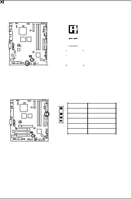
Connectors
J10: Ring Power On
1
(For 6CMC7)
1  (For 6CMC7R)
|
|
|
|
|
|
|
|
|
|
|
|
|
|
|
|
|
|
|
|
|
|
|
|
|
|
|
|
|
|
|
|
|
|
|
|
|
|
|
|
|
|
|
|
|
|
Pin No. |
Definition |
|
|
|
|
|
|
|
|
|
|
|
|
|
|
|
|
|
|
|
|
|
|
1 |
Signal |
|
|
|
|
|
|
|
|
|
|
|
|
|
|
|
|
|
|
|
|
|
|
||
|
|
|
|
|
|
|
|
|
|
|
|
|
|
|
|
|
|
|
|
|
|
||
|
|
|
|
|
|
|
|
|
|
|
|
|
|
|
|
|
|
|
|
|
|
||
|
|
|
|
|
|
|
|
|
|
|
|
|
|
|
|
|
|
|
|
|
|
2 |
GND |
|
|
|
|
|
|
|
|
|
|
|
|
|
|
|
|
|
|
|
|
|
|
||
|
|
|
|
|
|
|
|
|
|
|
|
|
|
|
|
|
|
|
|
|
|
|
|
J15 : External SMBUS Device Connector
1 |
Pin No. |
Definition |
|
1 |
SMB CLK |
||
|
|||
|
2 |
NC |
|
|
3 |
GND |
|
|
4 |
SMB DATA |
|
|
5 |
+5V |
20
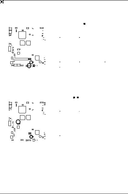
6CMC7/ 6CMC7R Motherboard
JP22 : Front Panel USB Port
|
2 |
|
|
10 |
|
||||||||||||||||||||||||||||||||||||||
|
|
|
|
|
|
|
|
|
|
|
|
|
|
|
|
|
|
|
|
|
|
|
|
|
|
|
|
|
|
|
|
|
|
|
|
|
|
|
|
|
|
|
|
|
|
|
|
|
|
|
|
|
|
|
|
|
|
|
|
|
|
|
|
|
|
|
|
|
|
|
|
|
|
|
|
|
|
|
|
|
|
|
|
|
|
|
|
|
|
|
|
|
|
|
|
|
|
|
|
|
|
|
|
|
|
|
|
|
|
|
|
|
|
|
|
|
|
1 |
|
|
9 |
|
|||||||||
|
|
|
|
|
|
|
|
|
|
|
|
|
|
|
|
|
|
|
|
|
|
|
|
|
|
|
|
|
|
|
|
|
|
|
|
|
|
|
|
|
|
|
|
|
|
|
|
|
|
|
|
|
|
|
|
|
|
|
|
|
|
|
|
|
|
|
|
|
|
|
|
|
|
Pin No. |
|
|
Definition |
||||||||||
|
|
|
|
|
|
|
|
|
|
|
|
|
|
|
|
|
|
|
|
|
|
|
|
|
|
|
|
|
|||||||||||||||
|
|
|
|
||||||||||||||||||||||||||||||||||||||||
|
|
|
|
|
|
|
|
|
|
|
|
|
|
|
|
|
|
|
|
|
|
|
|
|
|
|
|
1,4,5,10 |
|
|
|
|
|
|
|
NC |
|||||||
|
|
|
|||||||||||||||||||||||||||||||||||||||||
|
|
|
|
|
|
|
|
|
|
|
|
|
|
|
|
|
|
|
|
|
|
|
|
|
|
|
|
|
2 |
|
|
|
|
|
|
|
|
|
|
+5V |
|||
|
|
|
|
|
|
|
|
|
|
|
|
|
|
|
|
|
|
|
|
|
|
|
|
|
|
|
|
|
|
|
|
|
|
|
|
|
|
|
|
|
|
|
|
|
|
|
|
|
|
|
|
|
|
|
|
|
|
|
|
|
|
|
|
|
|
|
|
|
|
|
|
|
|
3,7,9 |
|
|
|
|
|
|
|
|
GND |
||||
|
|
|
|
|
|
|
|
|
|
|
|
|
|
|
|
|
|
|
|
|
|
|
|
|
|
|
|
|
|||||||||||||||
|
|
|
|
|
|
|
|
|
|
|
|
|
|
|
|
|
|
|
|
|
|
|
|
|
|
|
6 |
|
|
|
|
|
|
|
|
USBP1+ |
|||||||
|
|
|
|
|
|
|
|
|
|
|
|
|
|
|
|
|
|
|
|
|
|
|
|
|
|
|
|
|
|
|
|
|
|
|
|
|
|
||||||
|
|
|
|
|
|
|
|
|
|
|
|
|
|
|
|
|
|
|
|
|
|
|
|
|
|
|
|
|
|
8 |
|
|
|
|
|
|
|
|
USBP1- |
||||
|
|
|
|
|
|
|
|
|
|
|
|
|
|
|
|
|
|
|
|
|
|
|
|
|
|
|
|
||||||||||||||||
J19 : Audio PIN
|
2 |
|
|
8 |
|
|||||||||||||||||||||||||||||||||||||||||
|
|
|
|
|
|
|
|
|
|
|
|
|
|
|
|
|
|
|
|
|
|
|
|
|
|
|
|
|
|
|
|
|
|
|
|
|
|
|
|
|
|
|
|
|
|
|
|
|
|
|
|
|
|
|
|
|
|
|
|
|
|
|
|
|
|
|
|
|
|
|
|
|
|
|
|
|
|
|
|
|
|
|
|
|
|
|
|
|
|
|
|
|
|
|
|
|
|
|
|
|
|
|
|
|
|
|
|
|
|
|
|
|
|
|
|
|
|
|
|
|
|
|
|
|
|
|
|
|
|
|
|
|
|
|
|
|
|
|
|
|
|
|
|
|
|
|
|
|
|
|
|
|
|
|
|
|
|
|
|
|
|
|
|
|
|
|
|
|
|
|
|
|
|
|
1 |
|
|
7 |
|
||||||||
|
|
|
|
|
|
|
|
|
|
|
|
|
|
|
|
|
|
|
|
|
|
|
|
|
|
|
|
|
|
|
|
|
|
|
|
|
|
|
|
|
|
|
|
|
|
|
|
|
|
|
|
|
|
|
|
|
|
|
|
|
|
|
|
|
|
|
|
|
|
|
|
|
|
|
|
|
|
|
|
|
|
|
|
|
|
|
|
|
|
|
|
|
|
|
|
|
|
|
|
|
|
|
|
|
|
|
|
|
|
|
|
|
|
|
|
|
|
|
|
|
|
|
|
|
|
|
|
|
|
|
|
|
|
|
|
|
|
|
|
|
|
|
|
|
|
|
|
|
|
|
|
|
|
|
|
|
|
|
|
|
|
|
|
|
|
|
|
|
|
|
|
|
|
|
|
Pin No. |
|
|
Definition |
||||||||
|
|
|
|
|
|
|
|
|
|
|
|
|
|
|
|
|
|
|
|
|
|
|
|
|
|
|
|
|
|
|
|
1 |
|
|
|
|
|
|
|
Line out_L |
||||||
|
|
|
|
|
|
|
|
|
|
|
|
|
|
|
|
|
|
|
|
|
|
|
|
|
|
|
|
|
|
|
|
|
|
|
2 |
|
|
|
|
|
|
|
Line out_R |
|||
|
|
|
|
|
|
|
|
|
|
|
|
|
|
|
|
|
|
|
|
|
|
|
|
|
|
|
|
|
|
|
|
|
|
|
3,4,5,6 |
|
|
|
|
|
|
|
GND |
|||
|
|
|
|
|
|
|
|
|
|
|
|
|
|
|
|
|
|
|
|
|
|
|
|
|
|
|
|
|
|
|
|
|
|
|||||||||||||
|
|
|
|
|
|
|
|
|
|
|
|
|
|
|
|
|
|
|
|
|
|
|
|
|
|
|
|
|
|
|
7 |
|
|
|
|
|
|
|
|
|
+12V |
|||||
|
|
|
|
|
|
|
|
|
|
|
|
|
|
|
|
|
|
|
|
|
|
|
|
|
|
|
|
|
|
|
|
|
|
|
|
|
|
|
|
|
|
|
|
|
|
|
|
|
|
|
|
|
|
|
|
|
|
|
|
|
|
|
|
|
|
|
|
|
|
|
|
|
|
|
|
|
|
|
|
|
|
|
|
|
|
|
|
|
|
|
|
|
|
21
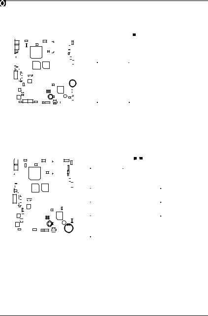
Connectors
J20 : CD/IN PIN
|
1 |
|
|
|
|
2 |
||||||||||||||||||||||||||||||||||||||
|
|
|
|
|
|
|
|
|
|
|
|
|
|
|
|
|
|
|
|
|
|
|
|
|
|
|
|
|
|
|
|
|
|
|
|
|
|
7 |
|
|
|
|
8 |
|
|
|
|
|
|
|
|
|
|
|
|
|
|
|
|
|
|
|
|
|
|
|
|
|
|
|
|
|
|
|
|
|
|
|
|
|
|
|
|
|
|
|
|||
|
|
|
|
|
|
|
|
|
|
|
|
|
|
|
|
|
|
|
|
|
|
|
|
|
|
|
|
|
|
|
|
|
|
|
|
|
|
|
|
|
|
|
|
|
|
|
|
|
|
|
|
|
|
|
|
|
|
|
|
|
|
|
|
|
|
|
|
|
|
|
|
|
|
|
|
|
|
|
|
|
|
|
|
Pin No. |
|
Definition |
|||
|
|
|
|
|
|
|
|
|
|
|
|
|
|
|
|
|
|
|
|
|
|
|
|
|
|
|
|
|
|
|
|
|
|
|
|
|
|
|
2 |
|
|
|
|
CD_L |
|
|
|
|
|
||||||||||||||||||||||||||||||||||||||||
|
|
|
|
|
|
|
|
|
|
|
|
|
|
|
|
|
|
|
|
|
|
|
|
|
|
|
|
|
|
|
|
|
|
|
|
|
|
|
3,7 |
|
|
|
|
VCC |
|
|
|
|
|
|
|
|
|
|
|
|
|
|
|
|
|
|
|
|
|
|
|
|
|
|
|
|
|
|
|
|
|
|
|
4,6 |
|
|
|
|
GND |
||||
|
|
|
|
|
|
|
|
|
|
|
|
|
|
|
|
|
|
|
|
|
|
|
|
|
|
|
|
|
|
|
|
|
|
|
|
|
|
|
|
|
|
|
|
|
|
|
|
|
|
|
|
|
|
|
|
|
|
|
|
|
|
|
|
|
|
|
|
|
|
|
|
|
|
|
|
|
|
|
|
|
|
|
|
8 |
|
|
|
|
CD_R |
|
|
|
|
|
|
|
|
|
|
|
|
|
|
|
|
|
|
|
|
|
|
|
|
|
|
|
|
|
|
|
|
|
|
|
|
|
|
|
|
|
|
|
|
|
J12: Smart Card Reader
|
|
|
|
|
|
|
|
|
|
|
|
|
|
|
|
|
|
|
|
|
|
|
|
|
|
|
|
|
2 |
|
|
|
|
|
|
|
|
|
|
|
|
|
14 |
|
|
|
|
|
|
|
|
|
|
|
|
|
|
|
|
|
|
|
|
|
|
|
|
|
|
|
|
|
|
|
|
|
|
|
|
|
|
|
|
|
|
||
|
|
|
|
|
|
|
|
|
|
|
|
|
|
|
|
|
|
|
|
|
|
|
|
|
|
|
|
|
1 |
|
|
|
|
|
|
|
|
|
|
|
|
|
13 |
|
|
|
|
|
|
|
|
|
|
|
|
|
|
|
|
|
|
|
|
|
|
|
|
|
|
|
|
|
Pin No. |
Definition |
|||||||||||||
|
|
|
|
|
|
|
|
|
|
|
|
|
|
|
|
|
|
|
|
|
|
|
|
|
|
|
|
|
2,3,4,8,9,13, |
|
NC |
||||||||||||
|
|
|
|
|
|
|
|
|
|
|
|
|
|
|
|
|
|
|
|
|
|
|
|
|
|
|
|
|
14 |
|
|
|
|
|
|||||||||
|
|
|
|
|
|
|
|
|
|
|
|
|
|
|
|
|
|
|
|
|
|
|
|
|
|
|
|
|
|
|
|
|
|
|
|
|
|
|
|
||||
|
|
|
|
|
|
|
|
|
|
|
|
|
|
|
|
|
|
|
|
|
|
|
|
|
|
|
|
|
1 |
|
|
|
|
|
|
VCC |
|||||||
|
|
|
|
|
|
|
|
|
|
|
|
|
|
|
|
|
|
|
|
|
|
|
|
|
|
|
|
|
5 |
|
|
|
|
|
|
SCRFET- |
|||||||
|
|
|
|
|
|
|
|
|
|
|
|
|
|
|
|
|
|
|
|
|
|
|
|
|
|
|
|
|
6 |
|
|
|
|
|
|
SCRRST |
|||||||
|
|
|
|
|
|
|
|
|
|
|
|
|
|
|
|
|
|
|
|
|
|
|
|
|
|
|
|
|
7 |
|
|
|
|
|
|
SCRCLK |
|||||||
|
|
|
|
|
|
|
|
|
|
|
|
|
|
|
|
|
|
|
|
|
|
|
|
|
|
|
|
|
|||||||||||||||
|
|
|
|
|
|
|
|
|
|
|
|
|
|
|
|
|
|
|
|
|
|
|
|
|
|
|
|
|
10 |
|
|
|
|
|
SCRIO |
||||||||
|
|
|
|
|
|
|
|
|
|
|
|
|
|
|
|
|
|
|
|
|
|
|
|
|
|
|
|
|
|||||||||||||||
|
|
|
|
|
|
|
|
|
|
|
|
|
|
|
|
|
|
|
|
|
|
|
|
|
|
|
|
|
11 |
|
|
|
|
|
GND |
||||||||
|
|
|
|
|
|
|
|
|
|
|
|
|
|
|
|
|
|
|
|
|
|
|
|
|
|
|
|
|
12 |
|
|
|
|
|
SCRPRES- |
||||||||
|
|
|
|
|
|
|
|
|
|
|
|
|
|
|
|
|
|
|
|
|
|
|
|
|
|
|
|
|
|
|
|
|
|
||||||||||
22
 Loading...