

Page 1
GE
Datasheet
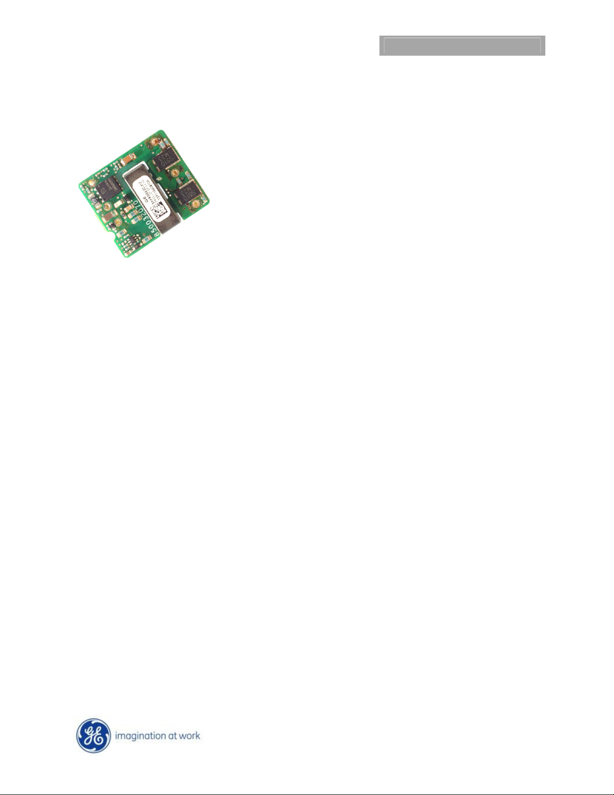
SHHN000A3 HAMMERHEAD* Series; DC-DC Converter Power Modules
9Vdc – 36Vdc input; +15V, -15V Dual Output, 0.3A 9W Output
Features
• Compliant to RoHS EU Directive 2002/95/EC (-Z
versions)
• Compliant to REACH Directive (EC) No 1907/2006
• Wide Input Voltage Range, 9Vdc to 36Vdc
• No minimum load for no damage operation
• Minimum efficiency – 84.0% at full load (Vin=24Vdc)
• Constant switching frequency
• Low output ripple and noise
• Small Size and low profile, follows industry standard
1x1 footprint
27.9mm x 24.4mm x 8.5mm (MAX)
(1.10 x 0.96 x 0.335 in)
• Surface mount (SMT) or Through hole (TH)
• Reflow process compliant, both SMT and TH versions
• Positive and Negative Remote On/Off logic
• Output overcurrent, overvoltage protection
• Over-temperature protection
• Wide operating temperature range (-40°C to 85°C)
#
Recognized to UL60950-1, CAN/CSA† C22.2
• UL
No.60950-1, and EN60950-1(VDE
• CE mark meets 2006/95/EC directive
‡
0805-1) Licensed
§
• Withstands 1600Vdc Isolation Voltage.
**
• ISO
9001 and ISO 14001 certified manufacturing
facilities
Applications
• Hybrid power architectures
• Industrial markets
RoHS Compliant
Description
The SHHN000A3A HAMMERHEAD* series power modules are isolated dc-dc converters that designed to operate over a wide input
voltage range of 9 Vdc -36Vdc and provide a single precisely regulated output voltage at +15.0Vdc and -15.0Vdc. The outputs are
fully isolated from the input, allowing versatile polarity configurations and grounding connections. The modules exhibit a
minimum efficiency of 84.0% at full load and nominal input. Built-in filtering for both input and output minimizes the need for
external filtering. The module is fully self-protected with output over-current and over-voltage, over-temperature and input under
voltage shutdown control. Optional features include negative or positive on/off logic and SMT connections.
*
Trademark of General Electric Corporation
#
UL is a registered trademark of Underwriters Laboratories, Inc.
†
CSA is a registered trademark of Canadian Standards Association.
‡
VDE is a trademark of Verband Deutscher Elektrotechniker e.V.
** ISO is a registered trademark of the International Organization of St andards
#
The PMBus name and logo are registered trademarks of the System Management Interface Forum (SMIF)
December 6, 2013
©2013 General Electric Corporation.
All rights reserved.
Page 2
GE
Datasheet
SHHN000A3 Series; DC-DC Converter Power Modules
9Vdc – 36Vdc input; +15V, -15V Dual Output, 0.3A 9W Output
Absolute Maximum Ratings
Stresses in excess of the absolute maximum ratings will cause permanent damage to the device. These are absolute stress ratings
only, functional operation of the device is not desired at these or any other conditions in excess of those given in the operations
sections of the Datasheet. Exposure to absolute maximum ratings for extended periods can adversely affect the device reliability.
Parameter Device Symbol Min Max Unit
Input Voltage (Continuous) All V
Transient (1s) – No damage All V
Operating Ambient Temperature All T
(see Thermal Considerations section)
Storage Temperature All T
Altitude All
I/O Isolation Voltage (100% factory Hi-Pot tested) All
IN
IN, trans
A
stg
⎯
Electrical Specifications
Unless otherwise indicated, specifications apply over all operating input voltage, resistive load, and temperature conditions .
Parameter Device Symbol Min Typ Max Unit
Operating Input Voltage All VIN 9
Maximum Input Current All I
(VIN=9 to 36V, IO1=I
Input No Load Current
= 24Vdc, IO = 0, module enabled)
(V
IN
Input Stand-by Current
= 24Vdc, module disabled)
(V
IN
O, max,
, IO2=I
)
O2 max,
= ON I
V
O1,02
All I
Inrush Transient All I
Input Reflected Ripple Current, peak-to-peak
(5Hz to 20MHz, 1μH source impedance; V
= I
; See Test Configurations)
&02
Omax
=0 to 36V, I
IN
O1
All 30 mAp-p
IN
IN,No load
9 mA
IN,stand-by
2
t 0.05 A2s
1
-0.3 40 Vdc
-0.3 50 Vdc
-40 85 °C
-55 125 °C
4000
⎯
1600
36 Vdc
m
Vdc
1.3 Adc
30 mA
Input Ripple Rejection (120Hz) All 40 dB
December 6, 2013
©2013 General Electric Corporation.
All rights reserved.
Page 2
Page 3
GE
Datasheet
SHHN000A3 Series; DC-DC Converter Power Modules
9Vdc – 36Vdc input; +15V, -15V Dual Output, 0.3A 9W Output
Electrical Specifications (continued)
Parameter Device Symbol Min Typ Max Unit
Output Voltage Set-point 1
(VIN=9 to 36Vdc, IO=I
O, max
, TA=25°C)
Output Voltage Set-point 2
(VIN=9 to 36Vdc, IO=I
O, max
, TA=25°C)
Output Voltage Accuracy
(Over all operating input voltage, resistive load, and temperature
conditions until end of life)
Output Regulation
Line (VIN=V
Load (IO=10% to I
Temperature (T
IN, min
to V
) All
IN, max
) All
O, max
to T
ref=TA, min
) All
A, max
Cross Regulation (10-100% Load on each output)** All 5 % V
Output Ripple and Noise on nominal output
Measured with 10uF Tantalum||1uF ceramic
(VIN=24 Vdc, IO=100%I
=25°C)
O, max, TA
RMS (5Hz to 20MHz bandwidth)
Peak-to-Peak (5Hz to 20MHz bandwidth)
External Capacitance All C
Output Current -1 All I
Output Current - 2 All I
Output Current Limit Inception (Hiccup Mode) All I
Output Short-Circuit Current
VO ≤ 250 mV @ 25°C
+15.0 V
-15.0 V
All V
V
O1
V
O2
O1, set
O2, set
O1, 02
-1.5% +1.5% %V0
-1.5% +1.5% %V0
-3.0
⎯
⎯
⎯ ⎯
⎯
0.05 0.3 % V
0.05 0.3 % V
+3.0 % V
1.0 % V
All
All I
O, max
o1
o2
O, lim
O, s/c
⎯
⎯
0
0
0
0.6 Adc
⎯
50 mV
200 mV
⎯
⎯
⎯
470 μF
0.3 Adc
0.3 Adc
0.4 A
O, set
rms
O, set
O, set
O, set
O, set
rms
pk-pk
Efficiency
=24Vdc, TA=25°C, IO=I
V
IN
O, max
Switching Frequency (Fixed)
VIN=9 to 36Vdc and IO= I
O, max
All η - 84
All f
sw
⎯
300
⎯
⎯
%
kHz
Dynamic Load Response
(ΔIO/Δt=0.1A/μs, VIN=24 Vdc, TA=25°C)
Load Change from IO= 50% to 75% or 25% to 50% of I
:
O,max
Peak Deviation All Vpk
Settling Time (Vo<10% peak deviation) All ts
* *Operation at 0A will not damage module
⎯
⎯
3.0
800
⎯
⎯
% V
μs
Isolation Specifications
Parameter Symbol Min Typ Max Unit
Isolation Capacitance C
Isolation Resistance R
iso
iso
I/O Isolation Voltage – (1minute at 1mA) All
⎯
200
1000
⎯ ⎯
⎯
⎯
1600 Vdc
pF
MΩ
December 6, 2013
©2013 General Electric Corporation.
All rights reserved.
Page 3
O, set
Page 4
GE
Datasheet
SHHN000A3 Series; DC-DC Converter Power Modules
9Vdc – 36Vdc input; +15V, -15V Dual Output, 0.3A 9W Output
General Specifications
Parameter Min Typ Max Unit
Calculated Reliability based upon Telcordia SR-332 Issue 2: Method I Case 3
=24Vdc, IO=80%xI
(V
IN
, TA=40°C, airflow = 200 LFM, 90% confidence)
O, max
Weight
FIT >=176.9 10
MTBF >=5,652,118 Hours
⎯
8 (0.28)
⎯
Feature Specifications
Unless otherwise indicated, specifications apply over all operating input voltage, resistive load, and temperature conditions. See
Feature Descriptions for additional information.
Parameter Device Symbol Min Typ Max Unit
Remote On/Off Signal Interface
(VIN=V
Signal referenced to V
Negative Logic: device code suffix “1”
Logic Low = module On, Logic High = module Off
Positive Logic: No device code suffix required
Logic Low = module Off, Logic High = module On
Turn-On Delay and Rise Times for each output
(IO=80% of I
Case 1: Input power is applied for at least 1second, and then the
On/Off input is set from OFF to ON (T
V
Case 2: On/Off input is set to Module ON, and then input power is
applied (T
Output voltage Rise time (time for Vo to rise from 10%
of V
Output Voltage Overshoot
(IO=80% of I
Output Overvoltage Protection
Input Undervoltage Lockout
to V
IN, min
Logic Low - Remote On/Off Current (V
; open collector or equivalent,
IN, max
terminal)
IN-
= -0.7Vdc) All I
on/off
Logic Low - On/Off Voltage All V
Logic High Voltage (I
= 0Adc) All V
on/off
Logic High maximum allowable leakage current All I
Logic Low - Remote On/Off Current (V
= -0.7Vdc) All I
on/off
Logic Low - On/Off Voltage All V
Logic High Voltage (I
= 0Adc) All V
on/off
Logic High maximum allowable leakage current All I
, TA=25°C)
O, max
= 10% of V
O
to 90% of V
o,set
= on/off pin transition until
)
O, set
= VIN reaches V
delay
)
o, set
, VIN= 9 to 36Vdc, TA=25°C)
O, max
delay
until VO = 10% of V
IN, min
O,set
)
All
All
All T
All V
Turn-on Threshold All V
Turn-off Threshold All V
Hysteresis All V
on/off
on/off
on/off
on/off
on/off
on/off
on/off
on/off
T
delay
Case1
T
delay
Case2
⎯ ⎯
-0.7
2.0
⎯
⎯
⎯ ⎯
⎯ ⎯
-0.7
2.0
⎯
⎯
⎯ ⎯
⎯
⎯
rise
⎯
25 ms
25 ms
25 ms
0.15 mA
0.8 Vdc
VIN V
25 μA
0.15 mA
0.8 Vdc
VIN V
25 μA
3 % V
O, limit
uv/on
uv/off
1.0 Vdc
hyst
140 %V
8.5 Vdc
7.5 Vdc
9
g (oz.)
/Hours
dc
dc
O, set
01,o2
December 6, 2013
©2013 General Electric Corporation.
All rights reserved.
Page 4
Page 5
GE
Datasheet
SHHN000A3 Series; DC-DC Converter Power Modules
9Vdc – 36Vdc input; +15V, -15V Dual Output, 0.3A 9W Output
Characteristic Curves
The following figures provide typical characteristics for the EHHD024A0A (5V, 24A) at 25 OC. The figures are identical for either
positive or negative remote On/Off logic.
90
Vin=24V
Vin=18V
Vin=36V
85
80
75
70
EFFICIENCY, η (%)
65
0 0.050.1 0.150.20.250.3
Vin=9V
OUTPUT CURRENT, IO (A) TIME, t (1ms/div)
Figure 1. Converter Efficiency versus Output Current.
Vin = 9V
Vin = 18V
Vin = 24V
- (50mV/div)
O
+ & V
O
Io(A) (100mA/div) V
OUTPUT CURRENT OUTPUT VOLTAGES
Figure 4. Transient Response to 0.1A/µS Dynamic Load
Change from 50% to 75% to 50% of full load, Vin=24V.
Vo+
- (5V/div)
O
+ & V
O
Vo+
-
Io
Vo-
(V) (100mV/div)
O+
OUTPUT VOLTAGE
V
TIME, t (2μs/div)
Figure 2. Typical output ripple and noise (V
(V) (100mV/div)
O-
OUTPUT VOLTAGE
Vin = 36V
, Io= I
o+
Remote
(V) (1V/div) V
o,max
). Figure 5. Typical Start-up Using Remote On/Off, negative logic
=
Vin = 18V
Vin=24V
Vin = 36V
ON/OFF
ON/OFF VOLTAGE OUTPUT VOLTAGES
V
version shown (V
- (5V/div)
O
+ & V
O
(V) (20V/div) V
IN
IN
= 24V, Io = I
TIME, t (10ms/div)
o,max
).
Vo+
Vin
Vo-
V
TIME, t (2µs/div) TIME, t (10ms/div)
INPUT VOLTAGE OUTPUT VOLTAGES
V
Figure 3. Typical output ripple and noise (Vo-, Io = Io,max). Figure 6. Typical Start-up Using Input Voltage (VIN= 24V, Io=
I
o,max
).
December 6, 2013
©2013 General Electric Corporation.
All rights reserved.
Page 5
Page 6

η
GE
SHHN000A3 Series; DC-DC Converter Power Modules
9Vdc – 36Vdc input; +15V, -15V Dual Output, 0.3A 9W Output
1.6
1.4
1.2
1
0.8
0.6
Input Current (A)
0.4
0.2
0
7 1217222732
Io min: 0A Io mid: 0.15A Io max: 0.3A
Input Voltage (V)
Figure 7. Input Current versus Input Voltage
Test Configurations
TO OSCILLOSCOPE
L
TEST
12μH
CURRENT PROBE
Vin+
R
R
contact
distribution
R
R
contact
distribution
NOTE: All voltage measurements to be taken at the module
terminals, as shown above. If sockets are used then
Kelvin connections are required at the module terminals
to avoid measurement errors due to socket contact
resistance.
Figure 10. Output Voltage and Efficiency Test Setup.
Vin+
V
IN
Vin-
V
Efficiency
=
VIN.I
Design Considerations
Vout+
Vout-
O.IO
IN
Datasheet
R
contact Rdistribution
R
contact Rdistribution
R
V
O
x 100 %
LOAD
CS 220μF
BATTERY
NOTE: Measure input reflected ripple current with a simulated
E.S.R.<0.1Ω
@ 20°C 100kHz
source induc tance (L
possible battery impedance. Measure current as shown
above.
TEST
33μF
Vin-
) of 12μH. Capacitor CS offsets
Figure 8. Input Reflected Ripple Current Test Setup.
COPPER STRIP
V
(+)
O
1uF .
V
( – )
O
NOTE: All voltage measurements to be taken at the module
terminals, as shown above. If sockets are used then
Kelvin connections are required at the module terminals
to avoid measurement errors due to socket contact
resistance.
10uF
GROUND PLANE
SC O P E
RESI STI V E
LO A D
Figure 9. Output Ripple and Noise Test Setup.
Input Source Impedance
The power module shall be connected to a low ac-impedance
source. Highly inductive source impedance can affect the
stability of the power module. For the test configuration in
Figure 8, a 33μF electrolytic capacitor (ESR<0.7Ω at 100kHz),
mounted close to the power module helps ensure the stability
of the unit
Safety Considerations
For safety-agency approval of the system in which the power
module is used, the power module shall be installed in
compliance with the spacing and separation requirements of
the end-use safety agency standard, i.e., UL 60950-1-3, CSA
C22.2 No. 60950-00, and VDE 0805 (IEC60950, 3
The input to these units is to be provided with a maximum 3A
fast-acting fuse in the ungrounded lead.
rd
Edition).
December 6, 2013
©2013 General Electric Corporation.
All rights reserved.
Page 6
Page 7

GE
SHHN000A3 Series; DC-DC Converter Power Modules
9Vdc – 36Vdc input; +15V, -15V Dual Output, 0.3A 9W Output
Feature Description
Remote On/Off
Two remote on/off options are available. Positive logic turns the
module on during a logic high voltage on the on/off pin, and off
during a logic low. Negative logic remote on/off, device code
suffix “1”, turns the module off during a logic high and on during
a logic low.
Vin+
I
on/off
V
on/off
Figure 11. Circuit configuration for using Remote On/Off
Implementation.
To turn the power module on and off, use a switch (open
collector or equivalent) to control the voltage (V
the ON/OFF terminal and the V
0V ≤ V
0.15mA, the switch should maintain a logic low level whilst
sinking this current.
During a logic high, the typical V
2.4V, and the maximum allowable leakage current at V
2.4V is 25μA.
If not using the remote on/off feature is designed such that:
For positive logic, leave the ON/OFF pin open.
For negative logic, short the ON/OFF pin to V
≤ 0.8V. The maximum I
on/off
ON/OFF
Vin-
Vout+
Common
Vout-
) between
(-) terminal. Logic low is
IN
during a logic low is
on/off
generated by the module is
on/off
on/off
(-).
IN
on/off
=
Overcurrent Protection
To provide protection in a fault (output overload) condition, the
unit is equipped with internal current-limiting circuitry and can
endure current limiting continuously. At the point of
current-limit inception, the unit shall enter hiccup mode. The
unit shall operate normally once the output current is brought
back into its specified range. The average output current during
hiccup is 10% I
O, max
.
Overtemperature Protection
To provide protection under certain fault conditions, the unit is
equipped with a thermal shutdown circuit. The unit shall
shutdown if the thermal reference point Tref (Figure 13),
exceeds 110°C. The module shall automatically restart upon
cool-down to a safe temperature.
Input Undervoltage Lockout
At input voltages below the input undervoltage lockout limit, the
module operation shall be disabled. The module will only begin
to operate once the input voltage is raised above the
undervoltage lockout turn-on threshold, V
the module shall continue to operate until the input voltage is
taken below the undervoltage turn-off threshold, V
Over Voltage Protection
The output overvoltage protection shall consist of circuitry that
independently monitors the output voltage, and shuts the
module down if the output voltage exceeds specified limits. The
module shall contain hiccup restart capability.
Datasheet
. Once operating,
UV/ON
UV/OFF
.
December 6, 2013
©2013 General Electric Corporation.
All rights reserved.
Page 7
Page 8

GE
SHHN000A3 Series; DC-DC Converter Power Modules
9Vdc – 36Vdc input; +15V, -15V Dual Output, 0.3A 9W Output
Thermal Considerations
The power modules shall operate in a variety of thermal
environments.
The thermal data shall be gathered based on physical
measurements taken in a wind tunnel, using automated
thermo-couple instrumentation to monitor key component
temperatures: FETs, diodes, control ICs, magnetic cores,
ceramic capacitors, opto-isolators, and module pwb
conductors, while controlling the ambient airflow rate and
temperature. For a given airflow and ambient temperature, the
module output power is increased, until one (or more) of the
components reaches its maximum derated operating
temperature, as defined in IPC-9592A. This procedure is then
repeated for a different airflow or ambient temperature until a
family of module output derating curves is obtained.
Figure 12. Thermal Test Setup .
The thermal reference point, T
used in the specifications shall
ref
be defined based on actual data. For reliable operation this
temperature should not exceed 110°C
Figure 13. T
Heat Transfer via Convection
Increased airflow over the module enhances the heat
transfer via convection. Derating curves showing the
maximum output current that can be delivered by
each module versus local ambient temperature (T
for natural convection are shown in Figures 14 - 15.
Please refer to the Application Note “Thermal Characterization
Process For Open-Frame Board-Mounted Power Modules” for a
detailed discussion of thermal aspects including maximum
device temperatures.
0.4
0.3
(A)
O
0.2
0.1
OUTPUT CURRENT, I
0.0
Figure 14. Output Current Derating for the Open Frame
Module; Airflow in the Transverse Direction from V
(+); VIN =18V, VO=+15V, -15V
V
out
Temperature Measurement Location.
ref
20 30 40 50 60 70 80 90
AMBIENT TEMEPERATURE, TA (oC)
Datasheet
Tref
A
)
NC
(-) to
out
December 6, 2013
©2013 General Electric Corporation.
All rights reserved.
Page 8
Page 9

GE
SHHN000A3 Series; DC-DC Converter Power Modules
9Vdc – 36Vdc input; +15V, -15V Dual Output, 0.3A 9W Output
0.4
(A)
0.3
O
0.2
0.1
OUTPUT CURRENT, I
0.0
20 30 40 50 60 70 80 90
AMBIENT TEMEPERATURE, TA (oC)
Figure 15. Output Current Derating for the Module with
Heatplate; Airflow in the Transverse Direction from V
V
(+);VIN =24V, VO=+15V, -15V
out
EMC Requirements
The design of the module shall include an external filter
configuration to meet the conducted emission limits of
EN55022 Class B. However, an onboard inductor shall be
provided in the module to meet Class B with modest external
filtering
NC
(-) to
out
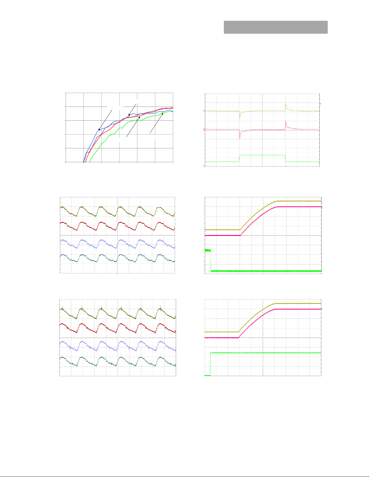
Figure 17. SHHN000A3 Vin+ Line EMC signature using above
filter, Vin=24V, Blue=PK, Red=Avg.
Datasheet
SHHN Series
Ref Des Filter
C1 , C2, C3 2.2uF/100V
C4, C5 33nF Y Cap
L1 4mH CM choke
L2 10uH inductor
Figure 16. Suggested Configuration for EN55022 Class B.
Figure 18. SHHN000A3 Vin Neutral EMC signature using
above filter, Vin=24V, Blue=PK, Red=Avg.
December 6, 2013
©2013 General Electric Corporation.
All rights reserved.
Page 9
Page 10

GE
SHHN000A3 Series; DC-DC Converter Power Modules
9Vdc – 36Vdc input; +15V, -15V Dual Output, 0.3A 9W Output
Layout Considerations
The SHHN000A3 power module series are low profile in order
to be used in fine pitch system card architectures. As such,
component clearance between the bottom of the power
module and the mounting board is limited. Avoid placing
copper areas on the outer layer directly underneath the power
module. Also avoid placing via interconnects underneath the
power module.
The SHHN000A3 family of power modules is available for
either Through-Hole (TH) or Surface Mount (SMT) soldering.
Through-Hole Soldering Information
The RoHS-compliant (Z codes) through-hole products use the
SAC (Sn/Ag/Cu) Pb-free solder and RoHS-compliant
components. They are designed to be processed through
single or dual wave soldering machines. The pins have an
RoHS-compliant finish that is compatible with both Pb and Pbfree wave soldering processes. A maximum preheat rate of
3°C/s is suggested. The wave preheat process should be such
that the temperature of the power module board is kept below
210°C. For Pb solder, the recommended pot temperature is
260°C, while the Pb-free solder pot is 270°C max. The Through
Hole module is also compatible with paste-in-hole reflow
soldering. Refer to the Reflow Soldering Information section for
process details. If additional information is needed, please
consult with your GE representative for more details.
Surface Mount Information
Pick and Place
The SHHN-SR series of DC-to-DC power converters use an
open-frame construction and are designed for surface mount
assembly within a fully automated manufacturing process.
The SHHN-SR series modules are designed to use the main
magnetic component surface to allow for pick and place.
14.5
[.57]
Note: All dimensions in mm [in].
Figure 19. Pick and Place Location.
15.2
[.60]
Z Plane Height
The ‘Z’ plane height of the pick and place location is 7.50mm
nominal with an RSS tolerance of +/-0.25 mm.
Nozzle Recommendations
The module weight has been kept to a minimum by using open
frame construction. Even so, they have a relatively large mass
when compared with conventional SMT components.
Variables such as nozzle size, tip style, vacuum pressure and
placement speed should be considered to optimize this
process.
The minimum recommended nozzle diameter for reliable
operation is 5mm. The maximum nozzle outer diameter, which
will safely fit within the allowable component spacing, is
6.5mm.
Oblong or oval nozzles up to 11 x 6 mm may also be used
within the space available.
For further information please contact your local GE Technical
Sales Representative.
Reflow Soldering Information
These power modules are large mass, low thermal
resistance devices and typically heat up slower than other
SMT components. It is recommended that the customer
review data sheets in order to customize the solder reflow
profile for each application board assembly.
The following instructions must be observed when SMT
soldering these units. Failure to observe these instructions
may result in the failure of or cause damage to the modules,
and can adversely affect long-term reliability.
There are several types of SMT reflow technologies currently
used in the industry. These surface mount power modules
can be reliably soldered using natural forced convection, IR
(radiant infrared), or a combination of convection/IR. The
recommended linear reflow profile using Sn/Pb solder is
shown in Figure 19 and 20. For reliable soldering the solder
reflow profile should be established by accurately
measuring the module’s pin connector temperatures.
300
250
200
150
10 0
REFLOW TEMP (°C)
50
0
Figure 20. Recommended Reflow Profile for Sn/Pb solder.
Pe ak Temp 235oC
Heat zone
oCs-1
max 4
Pr eheat zone
max 4
Datasheet
Soak zone
30-240s
oCs-1
REFLOW TIME (S)
T
205
lim
Co oling
zo ne
1- 4
above
o
C
oCs-1
December 6, 2013
©2013 General Electric Corporation.
All rights reserved.
Page 10
Page 11

GE
SHHN000A3 Series; DC-DC Converter Power Modules
9Vdc – 36Vdc input; +15V, -15V Dual Output, 0.3A 9W Output
240
235
230
225
220
215
210
MAX TEMP SOLDER (°C)
205
200
0 10203040 50 60
Figure 21. Time Limit, T
TIME LIMIT (S)
, Curve Above 205oC Reflow .
lim
Lead Free Soldering
The –Z version SMT modules of the SHHN000A3 series are
lead-free (Pb-free) and RoHS compliant and are compatible in
a
Pb-free soldering process. Failure to observe the instructions
below may result in the failure of or cause damage to the
modules and can adversely affect long-term reliability.
Pb-free Reflow Profile
Power Systems will comply with J-STD-020 Rev. D
(Moisture/Reflow Sensitivity Classification for Nonhermetic
Solid State Surface Mount Devices)
for both Pb-free solder profiles and MSL classification
procedures. This standard provides a recommended forcedair-convection reflow profile based on the volume and
thickness of the package (table 4-2). The suggested Pb-free
solder paste is Sn/Ag/Cu (SAC). The recommended linear reflow
profile using Sn/Ag/Cu solder is shown in Figure 22.
Surface Mount Information (continued)
300
Per J-STD-020 Rev. D
250
200
150
Heating Zone
1°C/Second
Reflow Temp (°C)
100
50
0
Figure 22. Recommended linear reflow profile using
Sn/Ag/Cu solder.
MSL Rating
The SHHN000A3 series SMT modules have a MSL rating of 2a.
Storage and Handling
The recommended storage environment and handling
procedures for moisture-sensitive surface mount packages is
detailed in J-STD-033 Rev. A (Handling, Packing, Shipping and
Use of Moisture/Reflow Sensitive Surface Mount Devices).
Moisture barrier bags (MBB) with desiccant are required for
MSL ratings of 2 or greater. These sealed packages should not
be broken until time of use. Once the original package is
broken, the floor life of the product at conditions of ≤ 30°C and
60% relative humidity varies according to the MSL rating (see
J-STD-033A). The shelf life for dry packed SMT packages will be
a minimum of 12 months from the bag seal date, when stored
at the following conditions: < 40° C, < 90% relative humidity.
Post Solder Cleaning and Drying Considerations
Post solder cleaning is usually the final circuit-board assembly
process prior to electrical board testing. The result of
inadequate cleaning and drying can affect both the reliability
of a power module and the testability of the finished
circuit-board assembly. For guidance on appropriate soldering,
cleaning and drying procedures, refer to GE Board Mounted
Power Modules: Soldering and Cleaning Application Note
(AP01-056EPS).
Peak Temp 260°C
Reflow Time (Seconds)
Datasheet
* Min. Time Abo ve 235°C
15 Seconds
*Time Above 217°C
60 Seconds
Cooling
Zone
December 6, 2013
©2013 General Electric Corporation.
All rights reserved.
Page 11
Page 12

GE
SHHN000A3 Series; DC-DC Converter Power Modules
9Vdc – 36Vdc input; +15V, -15V Dual Output, 0.3A 9W Output
Mechanical Outline for Through-Hole Module
Dimensions are in millimeters and [inches].
Tolerances: x.x mm ± 0.5 mm [x.xx in. ± 0.02 in.] (Unless otherwise indicated)
x.xx mm ± 0.25 mm [x.xxx in ± 0.010 in.]
*Top side label includes GE name, product designation and date code.
Top View
Datasheet
Side View
Bottom View
*For optional pin lengths, see Table 2, Device Options
VO+
VI+
VI-
ON/OFF
COMMON
VO-
December 6, 2013
©2013 General Electric Corporation.
All rights reserved.
Page 12
Page 13

GE
SHHN000A3 Series; DC-DC Converter Power Modules
9Vdc – 36Vdc input; +15V, -15V Dual Output, 0.3A 9W Output
Mechanical Outline for SMT version
Dimensions are in millimeters and [inches].
Tolerances: x.x mm ± 0.5 mm [x.xx in. ± 0.02 in.] (Unless otherwise indicated)
x.xx mm ± 0.25 mm [x.xxx in ± 0.010 in.]
*Top side label includes GE name, product designation and date code.
Top View
Datasheet
Side View
Bottom View
VI+
VI-
ON/OFF
VO+
COMMON
VO-
December 6, 2013
©2013 General Electric Corporation.
All rights reserved.
Page 13
Page 14

GE
SHHN000A3 Series; DC-DC Converter Power Modules
9Vdc – 36Vdc input; +15V, -15V Dual Output, 0.3A 9W Output
Recommended Pad Layout
Dimensions are in millimeters and [inches].
Tolerances: x.x mm ± 0.5 mm [x.xx in. ± 0.02 in.] (Unless otherwise indicated)
x.xx mm ± 0.25 mm [x.xxx in ± 0.010 in.]
Datasheet
Pin Fu nction
1 Vin+
2 Vin-
3 On/Off
4 Vout-
5 Common
6 Vout+
December 6, 2013
©2013 General Electric Corporation.
All rights reserved.
Page 14
Page 15

GE
Datasheet
SHHN000A3 Series; DC-DC Converter Power Modules
9Vdc – 36Vdc input; +15V, -15V Dual Output, 0.3A 9W Output
Packaging Details
The SHHN000A3 series SMT versions are supplied in tape & reel as standard. Details of tape dimensions are shown below.
Modules are shipped in quantities of 150 modules per reel.
Tape Dimensions
Dimensions are in millimeters and [inches].
Tolerances: x.x mm ± 0.5 mm [x.xx in. ± 0.02 in.] (unless otherwise indicated)
x.xx mm ± 0.25 mm [x.xxx in ± 0.010 in.]
.
The SHHN000A3 series Through Hole versions are supplied in trays as standard. Details of tray dimensions are shown
below. Modules are shipped in quantities of 75 modules per box.
Tray Dimensions
The SHHN000A3 - series Through Hole versions are supplied in trays as standard. Details of tray dimensions are shown
below. Modules are shipped in quantities of 75 modules per box.
Dimensions are in millimeters.
Tolerances: x.x mm ± 0.5 mm (unless otherwise indicated)
x.xx mm ± 0.25 mm
Material PET (1mm)
Max
surface
resistivity
Color Clear
Capacity
Min
order
quantity
9
10
-1011Ω/PET
25power
modules
75pcs (1 box of
3 full trays + 1
empty top tray)
December 6, 2013
©2013 General Electric Corporation.
All rights reserved.
Page 15
Page 16

GE
Datasheet
SHHN000A3 Series; DC-DC Converter Power Modules
9Vdc – 36Vdc input; +15V, -15V Dual Output, 0.3A 9W Output
Ordering Information
Please contact your GE Sales Representative for pricing, availability and optional features.
Table 1. Device Codes
Device Code
SHHN000A3CL41-SRZ 9 – 36Vdc +15V, -15V 0.3A Negative Yes 150031671
SHHN000A3CL4-SRZ 9 – 36Vdc +15V, -15V 0.3A Positive Yes 150031675
SHHN000A3CL41Z 9 – 36Vdc +15V, -15V 0.3A Negative No 150031070
SHHN000A3CL4Z 9 – 36Vdc +15V, -15V 0.3A Positive No 150031672
-Z refers to RoHS compliant parts
Table 2. Device Options
Characteristic Def inition
Form Factor S
Family Designator HH
Input Voltage N N = Wide Range, 9V-36V
Output Current 000A3 000A3 = 000.3 Amps Maximum Output Current
RatingsOptions
Output Voltage CL C= +15Volts, L = -15Volts
Pin Length
Action following
Protective Shutdown
On/Off Logic
Customer Specific XY
Mechanical Features
RoHS
Input
Voltage Range
Character and Position
6
8
4
1
Output
Voltage
SRS = Surface Mount connections: R = Tape & Reel Packaging
Output
Current
= 1 x 1 Brick
S
= Hammerhead* Series
HH
Omit = Default Pin Length shown in Mechanical Outline Figures
= Pin Length: 3.68 mm ± 0.25mm , (0.145 in. ± 0.010 in.)
6
= Pin Length: 2.79 mm ± 0.25mm , (0.110 in. ± 0.010 in.)
8
= Auto-restart following s hutdow n (Overcurrent/Overvoltage)
4
Must be ordered
Omit = Positive Logic
= Negative Logic
1
= Customer Specific Modified Code, Omit for Standard Code
XY
Omit = Standard open Frame Module
Omit = RoHS 5/6, Lead Based Solder Used
ZZ = RoHS 6/6 Compliant, Lead free
On/Off
Logic
Surface
Mount
Comcodes
Contact Us
For more information, call us at
USA/Canada:
+1 888 546 3243, or +1 972 244 9288
Asia-Pacific:
+86.021.54279977*808
Europe, Middle-East and Africa:
+49.89.878067-280
India:
+91.80.28411633
December 6, 2013 ©2012 General Electric Corporation. All rights reserved. Version 1.0
www.gecriticalpower.com
 Loading...