

Page 1
Data Sheet
March 27, 2008
LC/LW010- and LC/LW015-Series Power Modules:
18 Vdc to 36 Vdc or 36 Vdc to 75 Vdc Inputs, 10 W and 15 W
The LC/LW010- and LC/LW015-Series Power Modules use
advanced, surface-mount technology and deliver high-quality, compact, dc-dc conversion at an economical price.
Options
Features
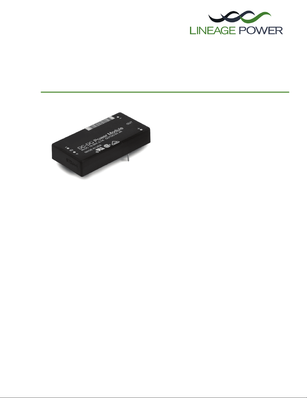
n Low profile: 10.2 mm x 25.4 mm x 50.8 mm
(0.4 in. x 1.0 in. x 2.0 in.) with standoffs
(9.6 mm (0.38 in.) with standoffs recessed)
n Wide input voltage range: 18 Vdc to 36 Vdc or
36 Vdc to 75 Vdc
n Output current limiting, unlimited duration
n Output overvoltage clamp
n Undervoltage lockout
n Input-to-output isolation: 1500 V
n Operating case temperature range: –40 °C to
+105 °C
n UL* 1950 Recognized, CSA
Certified, IEC950, and VDE0805 Licensed
n CE mark meets 73/23/EEC and 93/68/EEC
directives
n Within FCC and VDE Class A radiated limits
‡
†
22.2 No. 950-95
n Remote on-off
n Choice of on/off configuration
n Short pin: 2.8 mm ± 0.25 mm (0.110 in. ± 0.010 in.)
n Synchronization (cannot be ordered on units with
remote on/off)
n Output voltage adjust: 90% to 110% of VO, nom
(single outputs only)
n Tight output voltage tolerance
Applications
n Telecommunications
n Distributed power architectures
n Private branch exchange (PBX)
n Voice and data multiplexing
Description
The L Single- and Dual-Output-Series Power Modules are low-profile, dc-dc converters that operate over an
input voltage range of 18 Vdc to 36 Vdc or 36 Vdc to 75 Vdc and provide one or two precisely regulated outputs. The outputs are isolated from the input, allowing versatile polarity configurations and grounding connections. The modules have a maximum power rating of 10 W to 15 W and efficiencies of up to 84% for a 5 V
output and 82% for a 3.3 V output. Built-in filtering for both input and output minimizes the need for external filtering.
* UL is a registered trademark of Underwriters Laboratories, Inc.
† CSA is a registered trademark of Canadian Standards Association.
‡ This product is intended for integration into end-use equipment. All the required procedures for CE marking of end-use equipment should be followed. (The CE mark is placed on selected products.)
Page 2
LC/LW010- and LC/LW015-Series Power Modules:
18 Vdc to 36 Vdc or 36 Vdc to 75 Vdc Inputs, 10 W and 15 W
Data Sheet
March 27, 2008
Absolute Maximum Ratings
Stresses in excess of the absolute maximum ratings can cause permanent damage to the device. These are absolute stress ratings only. Functional operation of the device is not implied at these or any other conditions in excess
of those given in the operations sections of the data sheet. Exposure to absolute maximum ratings for extended
periods can adversely affect device reliability.
Parameter Device Symbol Min Typ Max Unit
Input Voltage:
Continuous
Transient (100 ms)
Operating Case Temperature
LC
LW
LW
VI, trans
All T
I
V
VI
C –40 — 105* °C
0
0
0
—
—
—
50
80
100
Vdc
Vdc
V
(See Derating Curves, Figures 43—45.)
Storage Temperature All T
stg –55 — 125 °C
I/O Isolation All — — — 1500 Vdc
* Maximum case temperature varies based on power dissipation. See derating curves, Figures 43—45, for details.
Electrical Specifications
Table 1. Input Specifications
Parameter Device Symbol Min Typ Max Unit
Operating Input Voltage LC
LW
Maximum Input Current
I = 0 to VI, max; IO = IO, max; see Figures
(V
LC
LW
V
I
VI
I
I, max
II, max
18
36
—
—
24
48
—
—
36
75
1.6
800
Vdc
Vdc
A
mA
1—4.)
Inrush Transient All
Input Reflected-ripple Current
All I
2
t
I
I —5—mAp-p
——0.2
A2s
(5 Hz to 20 MHz; 12 µH source impedance; T
A = 25 °C; see Figure 33.)
Input Ripple Rejection (100 Hz—120 Hz) All — — 45 — dB
Fusing Considerations
CAUTION: This power module is not internally fused. An input line fuse must always be used.
This encapsulated power module can be used in a wide variety of applications, ranging from simple stand-alone
operation to an integrated part of a sophisticated power architecture. To preserve maximum flexibility, internal fusing is not included; however, to achieve maximum safety and system protection, always use an input line fuse. The
safety agencies require a normal-blow, dc fuse with a maximum rating of 5 A (see Safety Considerations section).
Based on the information provided in this data sheet on inrush energy and maximum dc input current, the same
type of fuse with a lower rating can be used. Refer to the fuse manufacturer’s data for further information.
2 Lineage Power
Page 3

Data Sheet
March 27, 2008
18 Vdc to 36 Vdc or 36 Vdc to 75 Vdc Inputs, 10 W and 15 W
Electrical Specifications (continued)
Table 2. Output Specifications
LC/LW010- and LC/LW015-Series Power Modules:
Parameter
Output Voltage Set Point
I = VI, nom; IO = IO, max; TA = 25 °C)
(V
Output Voltage
(Over all line, load, and temperature
conditions until end of life; see
Figures 35 and 37.)
Device Code
or Suffix
D
G*
F
A
B
C
AJ
BK
CL
D
G*
F
A
B
C
AJ
BK
CL
Symbol Min Typ Max Unit
O, set
V
VO, set
VO, set
VO, set
VO, set
VO, set
VO1, set
VO2, set
VO1, set
VO2, set
VO1, set
VO2, set
O, set
V
VO, set
VO, set
VO, set
VO, set
VO, set
VO1, set
VO2, set
VO1, set
VO2, set
VO1, set
VO2, set
1.92
—
3.17
4.85
11.52
14.40
4.75
–4.75
11.40
–11.40
14.25
–14.25
1.90
—
3.13
4.80
11.40
14.25
4.5
–4.5
10.80
–10.80
13.50
–13.50
Output Regulation
(See Figures 5—11):
Line (V
Load (I
Load (I
I = VI, min to VI, max)
O = IO, min to IO, max)
O = IO, min to IO, max)
Temperature
C = –40 °C to +85 °C)
(T
A, F, D, G*
B, C
Lx010 A, F, D, G*
B, C
Lx015 A, F, D, G*
B, C
A, F, D, G*
B, C
—
—
—
—
—
—
—
—
—
—
—
—
—
—
—
—
Output Ripple and Noise
(Across 2 x 0.47 µF ceramic capacitors; see Figures 34 and 36.):
RMS
Peak-to-peak (5 Hz to 20 MHz)
External Load Capacitance A, F, D, G*
* For a 2.5 V output, use the 2 V output module (D code) with an output voltage trim pin (optional feature).
A, D, F, G*
AJ, B, C
BK, CL
A, D, F, G*
AJ, B, C
BK, CL
B, C
—
—
—
—
—
—
—
—
—
—
—
—
—
—
—
—
2.0
2.5
3.3
5.0
12.0
15.0
5.0
–5.0
12.0
–12.0
15.0
–15.0
—
2.5
—
—
—
—
—
—
—
—
—
—
—
0.01
—
0.1
—
0.1
25
0.5
—
—
—
—
—
—
—
—
2.08
—
3.43
5.20
12.48
15.60
5.25
–5.25
12.60
–12.60
15.75
–15.75
2.10
—
3.47
5.25
12.60
15.75
5.5
–5.5
13.20
–13.20
16.50
–16.50
5
0.1
10
0.2
15
0.2
100
2.0
30
35
50
100
120
150
1000
200
Vdc
Vdc
Vdc
Vdc
Vdc
Vdc
Vdc
Vdc
Vdc
Vdc
Vdc
Vdc
Vdc
Vdc
Vdc
Vdc
Vdc
Vdc
Vdc
Vdc
Vdc
Vdc
Vdc
Vdc
mV
O
%V
mV
O
%V
mV
O
%V
mV
O
%V
mVrms
mVrms
mVrms
mVp-p
mVp-p
mVp-p
µF
µF
Lineage Power 3
Page 4

LC/LW010- and LC/LW015-Series Power Modules:
18 Vdc to 36 Vdc or 36 Vdc to 75 Vdc Inputs, 10 W and 15 W
Electrical Specifications (continued)
Table 2. Output Specifications (continued)
Data Sheet
March 27, 2008
Parameter
Output Current
O < IO, min, the modules may
(At I
exceed output ripple specifications,
but operation is guaranteed.)
Note: On the Lx01xF, the output
voltage may exceed
specifications when
O <IO, min.
I
Output Current-limit Inception
O = 90% VO, set; see Figures
(V
12—14.)
Device Code
or Suffix
Lx015D
Lx015F
Lx015A
Lx015B
Lx015C
Lx010D, G*
Lx010F
Lx010A
Lx010B
Lx010C
Lx010AJ
Lx010BK
Lx010CL
Lx015D
Lx015F
Lx015A
Lx015B
Lx015C
Lx010D, G*
Lx010F
Lx010A
Lx010B
Lx010C
Symbol Min Typ Max Unit
O
I
IO
IO
IO
IO
IO
IO
IO
IO
IO
IO1, IO2
IO1, IO2
IO1, IO2
O
I
IO
IO
IO
IO
IO
IO
IO
IO
IO
0.35
0.25
0.15
0.12
0.10
0.2
0.15
0.1
0.08
0.06
0.1
0.06
0.05
—
—
—
—
—
—
—
—
—
—
—
—
—
—
—
—
—
—
—
—
—
—
—
—
—
—
—
—
—
—
—
—
—
3.0
3.0
3.0
1.25
1.0
2.0
2.42
2.0
0.83
0.67
1.0
0.42
0.33
7.5
6.5
5
3.1
2.5
7.0
5
4
2.5
2
A
A
A
A
A
A
A
A
A
A
A
A
A
A
A
A
A
A
A
A
A
A
A
Lx010AJ
Lx010BK
Lx010CL
Output Short-circuit Current
O = 0.25 V)
(V
Lx015D
Lx015F
Lx015A
Lx015B
Lx015C
Lx010D, G*
Lx010F
Lx010A
Lx010B
Lx010C
Lx010AJ
Lx010BK
Lx010CL
* For a 2.5 V output, use the 2 V output module (D code) with an output voltage trim pin (optional feature).
IO1, IO2
IO1, IO2
IO1, IO2
O
I
IO
IO
IO
IO
IO
IO
IO
IO
IO
IO1, IO2
IO1, IO2
IO1, IO2
—
—
—
—
—
—
—
—
—
—
—
—
—
—
—
—
—
—
—
—
—
—
—
—
—
—
—
—
—
—
—
—
4.0
2.5
2.5
8.5
8.5
7.5
4.5
4.5
8
7.5
6
3.5
3.5
6.0
3.5
3.5
A
A
A
A
A
A
A
A
A
A
A
A
A
A
A
A
4 Lineage Power
Page 5
Data Sheet
March 27, 2008
18 Vdc to 36 Vdc or 36 Vdc to 75 Vdc Inputs, 10 W and 15 W
Electrical Specifications (continued)
Table 2. Output Specifications (continued)
LC/LW010- and LC/LW015-Series Power Modules:
Parameter
Efficiency
I = VI, nom; IO = IO, max; TA = 25 °C;
(V
see Figures 15—28, 35, and 37.)
Efficiency
I = VI, nom; IO = 2 A; TA = 25 °C;
(V
see Figures 15, 18, 22, and 25.)
Device Code
or Suffix
LC015D
LC015F
LC015A
LC015B, C
LC010D, G*
LC010F
LC010A, B, C
LC010AJ, BK, CL
LW015D
LW015F
LW015A
LW015B, C
LW010D, G*
LW010F
LW010A, B, C
LW010AJ, BK, CL
LC015F
LC015A
LW015F
LW015A
Symbol Min Typ Max Unit
η
η
η
η
η
η
η
η
η
η
η
η
η
η
η
η
η
η
η
η
64
74
77
73
65
71
75
75
66
76
79
75
67
73
77
77
—
—
—
—
67
77
80
76
68
75
79
78
69
79
82
78
70
76
81
80
79
82
82
84
—
—
—
—
—
—
—
—
—
—
—
—
—
—
—
—
—
—
—
—
%
%
%
%
%
%
%
%
%
%
%
%
%
%
%
%
%
%
%
%
Switching Frequency All — — 265 — kHz
Dynamic Response
(for duals: I
O/Δt = 1A/10 µs; VI = VI, nom;
ΔI
A = 25 °C; see Figures 29 and 30.):
T
Load Change from I
of I
Peak Deviation
Settling Time
Load Change from I
of I
Peak Deviation
Settling Time
* For a 2.5 V output, use the 2 V output module (D code) with an output voltage trim pin (optional feature).
O1 or IO2 = IO, max;
O = 50% to 75%
O, max:
O < 10% of peak deviation)
(V
O = 50% to 25%
O, max:
O < 10% of peak deviation)
(V
All
All
All
All
—
—
—
—
—
—
—
—
2
0.8
2
0.8
—
—
—
—
%V
%V
O, set
ms
O, set
ms
Table 3. Isolation Specifications
Parameter Min Typ Max Unit
Isolation Capacitance — 600 — pF
Isolation Resistance 10 — — MΩ
Lineage Power 5
Page 6

LC/LW010- and LC/LW015-Series Power Modules:
18 Vdc to 36 Vdc or 36 Vdc to 75 Vdc Inputs, 10 W and 15 W
Data Sheet
March 27, 2008
Electrical Specifications (continued)
Table 4. General Specifications
Parameter Min Typ Max Unit
Calculated MTBF (I
Lx010
Lx015
Weight — — 28.3 (1.0) g (oz.)
Hand Soldering
(soldering iron 3 mm (0.125 in.) tip, 425 °C)
Table 5. Feature Specifications
O = 80% of IO, max; TC = 40 °C):
—
—
7,800,000
5,400,000
—
—
hours
hours
—— 12 s
Parameter
Remote On/Off Signal Interface (optional):
I = 0 V to VI, max; open collector or
(V
equivalent compatible; signal referenced to
I(–) terminal. See Figure 38 and Feature
V
Descriptions.):
Positive Logic— Device Code Suffix “4”:
Logic Low—Module Off
Logic High—Module On
Negative Logic— Device Code Suffix “1”:
Logic Low—Module On
Logic High—Module Off
Module Specifications:
On/Off Current—Logic Low
On/Off Voltage:
Logic Low
Logic High (I
on/off = 0)
Open Collector Switch Specifications:
Leakage Current During Logic High
on/off = 10 V)
(V
Output Low Voltage During Logic Low
on/off = 1 mA)
(I
Turn-on Delay and Rise Times
(At 80% of I
O, max; TA = 25 °C; see Figures 31
and 32.):
Case 1: On/Off Input Is Set for Unit On and
then Input Power Is Applied (delay from
point at which V
O, nom).
V
I = VI, min until VO = 10% of
Case 2: Input Power Is Applied for at Least
One Second, and then the On/Off Input Is
Set to Turn the Module On (delay from
point at which on/off input is toggled until
O = 10% of VO, nom).
V
Output Voltage Rise Time
(time for V
90% of V
O to rise from 10% of VO, nom to
O, nom)
Output Voltage Overshoot
(at 80% of I
O, max; TA = 25 °C)
Device Code
or Suffix
All
All
All
All
All
All
All
All
All
Symbol Min Typ Max Unit
on/off
I
Von/off
Von/off
Ion/off
Von/off
T
delay
Tdelay
Trise
—
—
–0.7
—
—
—
—
—
—
—
—
—
—
—
—
5
1
0.2
—
1.0
1.2
10
50
1.2
20
10
5
5
mA
V
V
µA
V
ms
ms
ms
%
6 Lineage Power
Page 7
Data Sheet
March 27, 2008
18 Vdc to 36 Vdc or 36 Vdc to 75 Vdc Inputs, 10 W and 15 W
Electrical Specifications (continued)
Table 5. Feature Specifications (continued)
LC/LW010- and LC/LW015-Series Power Modules:
Parameter
Output Voltage Set-point Adjustment Range
(optional: single outputs only)
Device Code
or Suffix
A, B, F
C
D
Output Overvoltage Clamp
O, clamp may be set higher on units with out-
(V
put voltage set-point adjustment option.)
D
F
A
B
C
AJ
BK
CL
Undervoltage Lockout LCxxx
LWxxx
Characteristic Curves
0.9
0.8
0.7
(A)
0.6
0.5
0.4
0.3
INPUT CURRENT, II
0.2
0.1
0.0
Figure 1. LC010 Input Current vs. Input Voltage at
5 10 15 2520 30
INPUT VOLTAGE, V
O = IO, max and TC = 25 °C
I
I (V)
35
8-1785(C)
400
Symbol Min Typ Max Unit
O, nom
%V
%VO, nom
%VO, nom
V
V
V
V
V
V
V
V
V
V
V
V
V
8-1786(C)
(A)
INPUT CURRENT, II
—
—
—
O, clamp
V
VO, clamp
VO, clamp
VO, clamp
VO, clamp
VO1, clamp
VO2, clamp
VO1, clamp
VO2, clamp
VO1, clamp
VO2, clamp
uvlo
V
Vuvlo
1.4
1.2
1.0
0.8
0.6
0.4
0.2
0.0
90
90
90
2.60
3.7
5.6
13.2
16.5
5.6
–5.6
13.2
–13.2
16.5
–16.5
11
20
5 10 15 3520 400 3025
INPUT VOLTAGE, VI (V)
—
—
—
—
—
—
—
—
—
—
—
—
—
—
14
27
110
100
125
4.0
5.7
7.0
16.0
21.0
7.0
–7.0
18.0
–18.0
21.0
–21.0
—
—
Figure 2. LC015 Input Current vs. Input Voltage at
O = IO, max and TC = 25 °C
I
Lineage Power 7
Page 8

LC/LW010- and LC/LW015-Series Power Modules:
18 Vdc to 36 Vdc or 36 Vdc to 75 Vdc Inputs, 10 W and 15 W
Data Sheet
March 27, 2008
Characteristics Curves (continued)
0.50
0.45
0.40
(A)
0.35
0.30
0.25
0.20
0.15
INPUT CURRENT, II
0.10
0.05
0.00
Figure 3. LW010 Input Current vs. Input Voltage at
(A)
INPUT CURRENT, II
10 20 30 5040 60
INPUT VOLTAGE, V
O = IO, max and TC = 25 °C
I
0.7
0.6
0.5
0.4
0.3
0.2
0.1
0.0
10 20 30 7040 800 6050
I (V)
70
800
8-1787(C)
5.15
(V)
5.10
5.05
VI = LOW LINE
VI = NOM LINE
VI = HIGH LINE
5.00
4.95
OUTPUT VOLTAGE 1, VO1
4.90
0.0
0.1 0.2 0.3
OUTPUT CURRENT 1, I
0.4
0.5 0.6
0.7
O1 (A)
0.8 0.9
Note: Output2 has characteristics similar to output1 when
I
O1 = 0.5 A and IO2 varies.
Figure 6. Lx010AJ Typical Load Regulation of
O2 = 0.5 A at
VI = NOM LINE
VI = HIGH LINE
(V)
Output1 with Fixed I
C = 25 °C
T
5.25
5.20
5.15
5.10
5.05
VI = LOW LINE
1.0
8-1790(C)
INPUT VOLTAGE, V I (V)
8-1788(C)
Figure 4. LW015 Input Current vs. Input Voltage at
O = IO, max and TC = 25 °C
I
)
1.003
set
1.002
1.001
1.000
0.999
0.998
0.997
NORMALIZED OUTPUT VOLTAGE (VO/VO,
0.1 0.2 0.6 0.7 0.8 0.9
NORMALIZED OUTPUT CURRENT (I
VI = LOW LINE
VI = NOM LINE
VI = HIGH LINE
0.4 0.50.3
1.00.0
O/IO, max)
8-1789(C)
Figure 5. Lx010x/Lx015x Single-Output Load
Regulation, Normalized Output Voltage
vs. Normalized Output Current at
C = 25 °C
T
5.00
OUTPUT VOLTAGE 1, VO1
4.95
0.1 0.2 0.6
0.4 0.50.3
OUTPUT CURRENT 2, I
0.7
O2 (A)
0.8 0.9
Note: Output2 has characteristics similar to output1 when
I
O2 = 0.1 A and IO1 varies.
Figure 7. Lx010AJ Typical Cross Regulation,
O1 vs. IO2 with Fixed IO1 = 0.1 A at
V
C = 25 °C
T
1.00.0
8-1791(C)
8
Lineage Power
Page 9

Data Sheet
March 27, 2008
LC/LW010- and LC/LW015-Series Power Modules:
18 Vdc to 36 Vdc or 36 Vdc to 75 Vdc Inputs, 10 W and 15 W
Characteristics Curves (continued)
5.00
4.95
(V)
O1
4.90
4.85
4.80
OUTPUT VOLTAGE 1, V
4.75
0.1 0.2 0.3 0.5 0.6 0.7
OUTPUT CURRENT 2, I
Note: Output2 has characteristics similar to output1 when
I
O2 = 1.0 A and IO1 varies.
Figure 8. Lx010AJ Typical Cross Regulation,
O1 vs. IO2 with Fixed IO1 = 1.0 A at
V
C = 25 °C
T
)
set
1.020
NORMALIZED OUTPUT VOLTAGE 1 (VO1/VO1,
1.016
1.013
1.010
1.006
1.003
1.000
0.996
0.993
0.990
IO = IO, min
NORMALIZED OUTPUT CURRENT (I
V
VI = LOW LINE
0.15 0.30 0.45 0.75 0.90
Note: Output2 has characteristics similar to output1 when
O1 = (0.5 * IO, max) and IO2 varies.
I
Figure 9. Lx010BK, CL Load Regulation of Output1
with Fixed I
Normalized V
VI = HIGH LINE
= NOM LINE
I
V
I
= LOW LINE
V
O2
(A)
O1/IO1, max)
0.8 0.9
IO = IO, max
0.4
I = NOM LINE
VI = HIGH LINE
0.60
O2 = 0.5 * IO, max at TC = 25 °C,
O1 vs. Normalized Current IO1
1.00.0
8-1792(C)
1.050.0
8-1793(C)
1.023
)
1.020
set
1.016
O1/VO1,
1.013
1.010
1.007
NORMALIZED
1.003
1.000
OUTPUT VOLTAGE 1 (V
0.996
IO = IO, min
VI = LOW LINE
VI = NOM LINE
VI = HIGH LINE
0.15 0.45 0.60 0.75 0.90 1.050.0 0.30
NORMALIZED OUTPUT CURRENT 2 (IO2/IO2, max)
IO = IO, max
8-1794(C)
Note: Output2 has characteristics similar to output1 when
I
O2 = IO, min and IO1 varies.
Figure 10. Lx010BK, CL Typical Cross Regulation,
Normalized V
Fixed I
1.006
1.000
0.993
O1/VO1, set)
0.987
0.980
0.973
NORMALIZED
0.966
0.960
OUTPUT VOLTAGE 1 (V
0.953
Note: Output2 has characteristics similar to output1 when
O2 = IO, max and IO1 varies.
I
O1 = IO, min at TC = 25 °C
IO = IO, min
0.15 0.45 0.60 0.75 0.90 1.050.0 0.30
NORMALIZED OUTPUT CURRENT 2 (IO2/IO2, max)
O1 vs. Normalized IO2 with
VI = LOW LINE
I = NOM LINE
V
= HIGH LINE
I
V
IO = IO, max
8-1795(C)
Figure 11. Lx010BK, CL Typical Cross Regulation,
Normalized V
Fixed I
O1 = IO, max at TC = 25 °C
O1 vs. Normalized IO2 with
Lineage Power
9
Page 10

LC/LW010- and LC/LW015-Series Power Modules:
18 Vdc to 36 Vdc or 36 Vdc to 75 Vdc Inputs, 10 W and 15 W
Data Sheet
March 27, 2008
Characteristics Curves (continued)
1.2
1.0
0.8
0.6
0.4
0.2
0.0
0.00
NORMALIZED OUTPUT VOLTAGE (VO/VO, set)
OUTPUT CURRENT NORMALIZED TO I
Figure 12. Lx010x/Lx015x Single-Output
VI = LOW LINE
I = NOM LINE
V
= HIGH LINE
V
I
0.25 0.50 0.75 1.00
1.25
1.50 1.75
O, max (IO/IO, max)
Normalized Output Current vs.
Normalized Output Voltage at
C = 25 °C
T
2.00
8-1796(C)
)
set
1.0
0.5
0.0
NORMALIZED OUTPUT VOLTAGE 1 (VO1/VO1,
V
I = LOW LINE
VI = NOM LINE
I = HIGH LINE
V
0.5 1.0 1.5 3.52.0 4.00.0 3.02.5
NORMALIZED OUTPUT CURRENT 1
WITH OUTPUT CURRENT 2
SET TO I
O, max (IO1/IO1, max)
8-1798(C)
Note: Output2 has characteristics similar to output1 when
output1 is set to I
O, max.
Figure 14. Lx010xx Dual-Output Normalized Output
Current vs. Normalized Output Voltage
C = 25 °C with Other Output at
at T
O = IO, max
I
1.0
)
set
O1/VO1,
0.5
VI = NOM LINE
NORMALIZED
OUTPUT VOLTAGE 1 (V
0.0
0.5 1.0 1.5 2.0 2.5 3.0
NORMALIZED OUTPUT CURRENT 1
VI = LOW LINE
I = HIGH LINE
V
WITH OUTPUT CURRENT 2
SET TO I
O, min (IO1/IO1, max)
4.50.0 3.5 4.0
8-1797(C)
Note: Output2 has characteristics similar to output1 when
output1 is set to I
O, min.
Figure 13. Lx010xx Dual-Output Normalized Output
Current vs. Normalized Output Voltage
C = 25 °C with Other Output at IO, min
at T
84
82
(%)
80
78
76
EFFICIENCY, η
74
72
70
0.0
0.5 1.0 1.5 2.0
OUTPUT CURRENT, I
I = 18 V
V
VI = 20 V
VI = 27 V
VI = 36 V
O (A)
2.5863.0
8-1800(C)
Figure 15. LC015A Typical Efficiency vs. Output
Current at T
C = 25 °C
10
Lineage Power
Page 11

Data Sheet
March 27, 2008
LC/LW010- and LC/LW015-Series Power Modules:
18 Vdc to 36 Vdc or 36 Vdc to 75 Vdc Inputs, 10 W and 15 W
Characteristics Curves (continued)
80
(%)
75
70
EFFICIENCY, η
65
60
0.0
0.16 0.32 0.48 0.64
NORMALIZED OUTPUT CURRENT (I
Figure 16. LC015B, C Typical Efficiency vs.
Normalized Output Current at T
72
70
68
(%)
66
64
EFFICIENCY, η
62
60
58
0.5 1 21.5 2.5 30
OUTPUT CURRENT, I
Figure 17. LC010D and LC015D Typical Efficiency
vs. Output Current at T
82
80
78
(%)
76
74
EFFICIENCY, η
72
70
0.5 1.0 1.5 2.0 2.5 3.0
0.0
VI = 18 V
VI = 27 V
VI = 36 V
O (A)
C = 25 °C
0.80850.96
O/IO, max
)
VI = 36 V
I = 27 V
V
V
I = 18 V
VI = 36 V
V
I
= 27 V
V
I
= 18 V
8-1801(C)
C = 25 °C
8-2049(C)
82
80
(%)
78
76
74
EFFICIENCY, η
72
70
0.1 0.2 0.4
NORMALIZED OUTPUT CURRENT (I
0.3
0.5
VI = 36 V
V
V
0.6 0.7
O/IO, max)
I = 27 V
I = 18 V
0.8 0.9
1.00.0
8-1803(C)
Figure 19. LC010A, B, C Typical Efficiency vs.
Normalized Output Current at T
80
75
70
(%)
65
60
55
EFFICIENCY, η
50
45
40
0.5 1.0 1.5 2.0 2.50.0
OUTPUT CURRENT, I
VI = 36 V
I
= 27 V
V
V
I
= 18 V
(A)
O
C = 25 °C
8-1804(C)
Figure 20. LC010F Typical Efficiency vs. Output
Current at T
80
78
76
74
(%)
72
70
68
66
EFFICIENCY, η
64
62
60
0.10
0.23 0.35 0.47 0.710.59 0.83
C = 25 °C
VI = 36 V
I = 24 V
V
V
I = 18 V
NORMALIZED OUTPUT CURRENT,
I
O1 = IO2 [(IO1 + IO2)/(IO1, max + IO2, max)]
0.95
8-1805(C)
OUTPUT CURRENT, I
O
(A)
8-1802(C)
Figure 18. LC015F Typical Efficiency vs. Output
Current at T
C = 25 °C
Lineage Power
Figure 21. LC010AJ, BK, CL Typical Efficiency vs.
Normalized Output Current at T
C = 25 °C
11
Page 12

LC/LW010- and LC/LW015-Series Power Modules:
18 Vdc to 36 Vdc or 36 Vdc to 75 Vdc Inputs, 10 W and 15 W
Data Sheet
March 27, 2008
Characteristics Curves (continued)
90
85
80
75
70
EFFICIENCY, η (%)
65
60
0.0 0.5 3.0
1.0 1.5 2.0 2.5
OUTPUT CURRENT, I
Figure 22. LW015A Typical Efficiency vs. Output
Current at T
82
80
78
76
74
EFFICIENCY, η (%)
72
70
0.05 0.19 1.0
NORMALIZED OUTPUT CURRENT (I
C = 25 °C
0.33 0.5 0.66 0.83
Figure 23. LW015B, C Typical Efficiency vs.
Normalized Output Current at T
80
70
60
50
40
30
EFFICIENCY, η (%)
20
10
0.0 0.5 3.0
1.0 1.5 2.0 2.5
OUTPUT CURRENT, I
Figure 24. LW010D, 015D Typical Efficiency vs.
Output Current at T
I = 75 V
V
VI = 48 V
VI = 36 V
I = 75 V
V
VI = 48 V
VI = 36 V
O (A)
I = 75 V
V
VI = 48 V
VI = 36 V
O/IO,
O (A)
C = 25 °C
max
)
8-1864(C)
8-1863(C)
C = 25 °C
8-1862(C)
85
80
75
I = 75 V
70
EFFICIENCY, η (%)
65
60
0.0 0.5 3.0
1.0 1.5 2.0 2.5
OUTPUT CURRENT, I
V
VI = 48 V
VI = 36 V
O (A)
8-1861(C)
Figure 25. LW015F Typical Efficiency vs. Output
Current at T
82
80
78
76
74
EFFICIENCY, η (%)
72
70
0.0 0.14 1.0
NORMALIZED OUTPUT CURRENT (IO/IO,
C = 25 °C
0.20 0.43 0.57 0.71
I = 75 V
V
VI = 48 V
VI = 36 V
0.86
max
)
8-1860(C)
Figure 26. LW010A, B, C Typical Efficiency vs.
C = 25 °C
8-1859(C)
80
78
76
74
72
70
68
66
EFFICIENCY, η (%)
64
62
60
0.0 0.5
Normalized Output Current at T
I
= 75 V
V
VI = 48 V
VI = 36 V
1.0 1.5 2.0 2.5
OUTPUT CURRENT, I
O
(A)
Figure 27. LW010F Typical Efficiency vs. Output
Current at T
C = 25 °C
1212 Lineage Power
Page 13

Data Sheet
March 27, 2008
18 Vdc to 36 Vdc or 36 Vdc to 75 Vdc Inputs, 10 W and 15 W
Characteristics Curves (continued)
85
LC/LW010- and LC/LW015-Series Power Modules:
80
75
EFFICIENCY, η (%)
70
65
60
0.2 0.3 0.9 1.0
0 0.1
NORMALIZED OUTPUT CURRENT,
I
O1 = IO2 [(IO1 + IO2)/(IO1, max + IO2, max)]
0.4 0.5 0.6 0.7 0.8
I = 75 V
V
VI = 48 V
VI = 36 V
8-1858(C)
Figure 28. LW010AJ, BK, CL Typical Efficiency vs.
Normalized Output Current at T
1.01
NORMALIZED
1.0
0.99
OUTPUT VOLTAGE (VO/VO, set)
0.75
)
0.50
max
(IO/IO,
LOAD CURRENT
TIME, t (100 µs/div)
C = 25 °C
8-1857(C)
Figure 29. Single-Output Typical Output Voltage for
Step Load Change from 50% to 75% of
O = IO, max
I
1.0
0
O1/VO1, set DUAL OUTPUTS
O/VO, set SINGLE OUTPUTS,
1.0
V
V
NORMALIZED OUTPUT VOLTAGE;
)
nom
I/VI,
(V
INPUT VOLTAGE
0
TIME, t (2 ms/div)
8-1806(C)
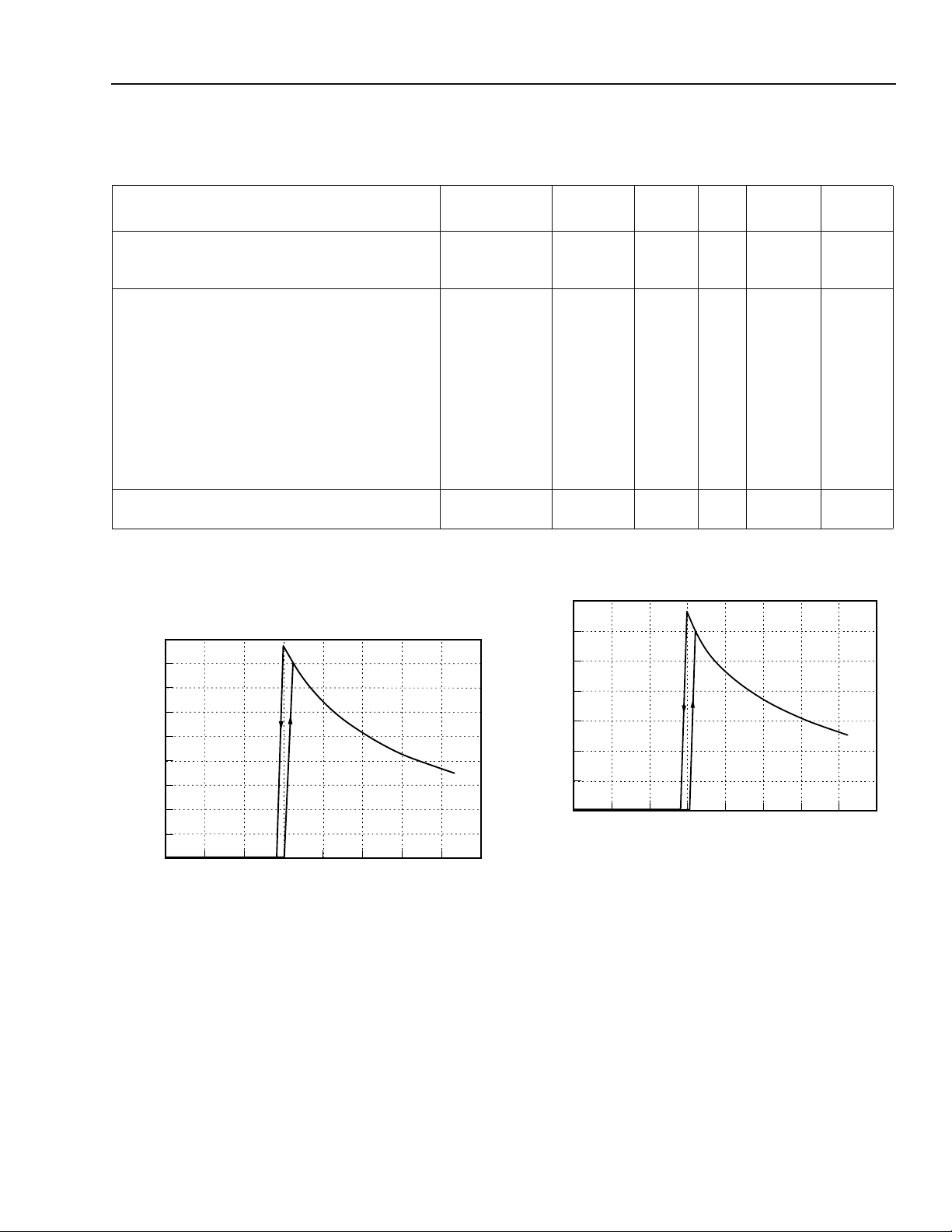
Figure 31. Typical Output Voltage Start-Up when
Input Voltage Is Applied; I
I
1.0
NORMALIZED
OUTPUT VOLTAGE;
O1/VO1, set DUAL OUTPUTS
O/VO, set SINGLE OUTPUTS,
0.0
V
V
O, max, VI = Nominal Line
O = 80% of
4.0
ON/OFF (V)
(2 V/div)
V
2.0
O/VO, set)
REMOTE ON/OFF,
0
1.01
NORMALIZED
1.0
0.99
OUTPUT VOLTAGE(V
0.50
)
0.25
max
O/IO,
(I
LOAD CURRENT
TIME, t (100 µs/div)
8-1856(C)
Figure 32. Typical Output Voltage Start-Up when
Signal Is applied to Remote On/Off;
O = 80% of IO, max
I
TIME, t (1 ms/div)
8-1807(C).a
Figure 30. Single-Output Typical Output Voltage for
Step Load Change from 50% to 25% of
O =IO, max
I
Lineage Power 13
Page 14

LC/LW010- and LC/LW015-Series Power Modules:
2
18 Vdc to 36 Vdc or 36 Vdc to 75 Vdc Inputs, 10 W and 15 W
Test Configurations
BATTERY
TO OSCILLOSCOPE
S
220 µF
C
IMPEDANCE < 0.1 Ω
@ 20 ˚C, 100 kHz
12 µH
CURRENT
33 µF
PROBE
I
(+)
V
V
I
(-)
L
TEST
VO1(+
COM
VO2(-)
)
COPPER STRIP
0.47 µF
0.47 µF
Data Sheet
March 27, 2008
0.47 µF
0.47 µF
SCOPE
SCOPE
R
R
LOAD1
LOAD2
8-203(C)
Note: Input reflected-ripple current is measured with a simulated
source impedance of 12 µH. Capacitor Cs offsets possible
battery impedance. Current is measured at the input of the
module.
Figure 33. Input Reflected-Ripple Test Setup
COPPER STRIP
VO(+)
0.47 µF
V
O(–)
0.47 µF
SCOPE
RESISTIVE
LOAD
8-513(C).g
Note: Use two 0.47 µF ceramic capacitors. Scope measurement
should be made using a BNC socket. Position the load
between 50 mm and 75 mm (2 in. and 3 in.) from the module.
Figure 34. Peak-to-Peak Output Noise
Measurement Test Setup for Single
Outputs
CONTACT AND
VI(+)
V
O(+)
I IO
I
SUPPLY
V
I(-)
CONTACT RESISTANCE
V
Note: All measurements are taken at the module terminals. When
socketing, place Kelvin connections at module terminals to
avoid measurement errors due to socket contact resistance.
O(+) VO(–)–[]IO
V
⎛⎞
------------------------------------------------
η
⎝⎠
VI (+) VI (–)–[]II
DISTRIBUTION LOSSES
O(-)
×=
LOAD
8-204(C)
100
8-808(C).d
Note: Use four 0.47 µF ceramic capacitors. Scope measurement
should be made using a BNC socket. Position the load
between 50 mm and 75 mm (2 in. and 3 in.) from the module.
Figure 36. Peak-to-Peak Output Noise
Measurement Test Setup for Dual
Outputs
CONTACT AND
DISTRIBUTION LOSSES
O1
IO
LOAD
LOAD
8-863(C).a
SUPPLY
CONTACT
RESISTANCE
VI(+)
I
I
VI(-)
V
COM
VO2
Note: All measurements are taken at the module terminals. When
socketing, place Kelvin connections at module terminals to
avoid measurement errors due to socket contact resistance.
VOJ COM–[]IOJ
∑
J1=
η
---------------------------------------------------
VI +() VI –()–[]II
x100=
Figure 37. Output Voltage and Efficiency
Measurement Test Setup for Dual
Outputs
Figure 35. Output Voltage and Efficiency
Measurement Test Setup for Single
Outputs
1414 Lineage Power
Page 15

Data Sheet
March 27, 2008
LC/LW010- and LC/LW015-Series Power Modules:
18 Vdc to 36 Vdc or 36 Vdc to 75 Vdc Inputs, 10 W and 15 W
Design Considerations
Input Source Impedance
The power module should be connected to a low
ac-impedance input source. Highly inductive source
impedances can affect the stability of the power module. If the source inductance exceeds 4 µH, a 33 µF
electrolytic capacitor (ESR < 0.7 Ω at 100 kHz)
mounted close to the power module helps ensure
stability of the unit.
Safety Considerations
For safety-agency approval of the system in which the
power module is used, the power module must be
installed in compliance with the spacing and separation
requirements of the end-use safety agency standard,
i.e., UL 1950, CSA 22.2 No. 950-95, EN60950, and
IEC950.
For the converter output to be considered meeting the
requirements of safety extra-low voltage (SELV), one of
the following must be true of the dc input:
n All inputs are SELV and floating, with the output also
floating.
n All inputs are SELV and grounded, with the output
also grounded.
n Any non-SELV input must be provided with rein-
forced insulation from any other hazardous voltages,
including the ac mains, and must have a SELV reliability test performed on it in combination with the
converters.
The power module has extra-low voltage (ELV) outputs
when all inputs are ELV.
Current Limit
To provide protection in a fault (output overload) condition, the unit is equipped with internal current-limiting
circuitry and can endure current limiting for an unlimited duration. At the point of current-limit inception, the
unit shifts from voltage control to current control. If the
output voltage is pulled very low during a severe fault,
the current-limit circuit can exhibit either foldback or
tailout characteristics (output-current decrease or
increase). The unit operates normally once the output
current is brought back into its specified range.
Remote On/Off (Optional)
Two remote on/off options are available. Positive logic,
device code suffix “4”, remote on/off turns the module
on during a logic-high voltage on the remote ON/OFF
pin, and off during a logic low. Negative logic, device
code suffix “1”, remote on/off turns the module off during a logic high and on during a logic low.
To turn the power module on and off, the user must
supply a switch to control the voltage between the
on/off terminal and the V
switch may be an open collector or equivalent (see
Figure 38). A logic low is V
maximum I
on/off during a logic low is 1 mA. The switch
should maintain a logic-low voltage while sinking 1 mA.
During a logic high, the maximum V
the power module is 10 V. The maximum allowable
leakage current of the switch at V
The module has internal capacitance to reduce noise
at the ON/OFF pin. Additional capacitance is not generally needed and may degrade the start-up characteristics of the module.
I(–) terminal (Von/off). The
on/off = –0.7 V to +1.2 V. The
on/off generated by
on/off = 10 V is 50 µA.
The input to these units is to be provided with a maximum 5 A normal-blow fuse in the ungrounded lead.
V
I(+)
I(-)
V
Feature Descriptions
Output Overvoltage Clamp
The output overvoltage clamp consists of control cir-
-
Von/off
+
Ion/off
REMOTE
ON/OFF
cuitry, independent of the primary regulation loop, that
monitors the voltage on the output terminals. This control loop has a higher voltage set point than the primary
8-758(C).a
loop (see Feature Specifications table). In a fault condition, the overvoltage clamp ensures that the output
voltage does not exceed V
O, clamp, max. This provides a
Figure 38. Remote On/Off Implementation
redundant voltage-control that reduces the risk of
output overvoltage.
Lineage Power 15
Page 16

LC/LW010- and LC/LW015-Series Power Modules:
18 Vdc to 36 Vdc or 36 Vdc to 75 Vdc Inputs, 10 W and 15 W
Data Sheet
March 27, 2008
Feature Descriptions (continued)
Output Voltage Adjustment (Optional on Single-Output Units)
Output voltage set-point adjustment allows the user to
increase or decrease the output voltage set point of a
module. This is accomplished by connecting an external resistor between the TRIM pin and either the V
O(–) pins. With an external resistor between the
or V
TRIM and V
point (V
O(+) pins (Radj-down), the output voltage set
O, adj) decreases (see Figure 39). The following
equation determines the required external resistor
value to obtain an output voltage change from V
O, adj:
to V
adj-down
R
where R
adj-down is the resistance value connected
between TRIM and V
VO adj, L–()G
---------------------------------------
Onom, VO adj,–()
V
O(+), and G, H, and L are defined
H– Ω=
in the following table.
VI (+)
V
O (+)
Radj-down
O(+)
O, nom
GHK L
Lx010, 5A 5110 2050 2.5 2.5
Lx010, 5B 10,000 5110 9.5 2.5
Lx010, 5C 10,000 5110 NA 2.5
Lx010, 5D 5110 2050 0.76 1.23
Lx010, 5F 5110 2050 0.75 2.5
The combination of the output voltage adjustment
and the output voltage tolerance cannot exceed 110%
(125% for the D) of the nominal output voltage between
O(+) and VO(–) terminals.
the V
VI(+)
V
I(-)
O(+)
V
TRIM
O(-)
V
RLOAD
Radj-up
8-715(C).d
Figure 40. Circuit Configuration to Increase Output
Volta g e
TRIM
V
I (–)
O(-)
V
RLOAD
8-715(C).e
Figure 39. Circuit Configuration to Decrease
Output Voltage
With an external resistor connected between the TRIM
O(–) pins (Radj-up), the output voltage set point
and V
O, adj) increases (see Figure 40). The following equa-
(V
tion determines the required external resistor value to
obtain an output voltage from V
Radj-up
where R
⎛⎞
-----------------------------------------
⎝⎠
adj-up is the resistance value connected
between TRIM and V
GL
Oadj, L–()K–[]
V
O (–), and the values of G, H, K,
O, nom to VO, adj:
H–
Ω=
and L are shown in the following table:
The L-Series power modules have a fixed current-limit
set point. Therefore, as the output voltage is adjusted
down, the available output power is reduced. In addition, the minimum output current is a function of the
output voltage. As the output voltage is adjusted down,
the minimum required output current can increase
(i.e., minimum power is constant).
Synchronization (Optional)
With external circuitry, the unit is capable of synchronization from an independent time base with a switching
rate of 256 kHz. Other frequencies may be available;
please consult the factory for application guidelines
and/or a description of the external circuit needed to
use this feature.
1616 Lineage Power
Page 17

Data Sheet
March 27, 2008
LC/LW010- and LC/LW015-Series Power Modules:
18 Vdc to 36 Vdc or 36 Vdc to 75 Vdc Inputs, 10 W and 15 W
Thermal Considerations
The power module operates in a variety of thermal
environments; however, sufficient cooling should be
provided to help ensure reliable operation of the unit.
Heat-dissipating components inside the unit are thermally coupled to the case. Heat is removed by conduction, convection, and radiation to the surrounding
environment. Proper cooling can be verified by measuring the case temperature. The case temperature
C) should be measured at the position indicated in
(T
Figures 41 and 42.
15.2
(0.6)
10.2
(0.4)
-
IN
+
Note: Dimensions are in millimeters and (inches). Pin locations are
for reference only.
LW010/LC010
dc-dc POWER MODULE
Figure 41. LW010 and LC010 Case Temperature
Measurement Location
-
OUT
+
8-1363(C).b
Heat Transfer Characteristics
Increasing airflow over the module enhances the heat
transfer via convection. Figures 43 through 45 show
the maximum power that can be dissipated by the module without exceeding the maximum case temperature
versus local ambient temperature (T
–1
vection through 3.0 ms
(600 ft./min.).
Systems in which these power modules are used typically generate natural convection airflow rates of
0.25 ms
–1
(50 ft./min.) due to other heat dissipating
components in the system. Therefore, the natural convection condition represents airflow rates of approximately 0.25 ms
–1
(50 ft./min.). Use of Figure 43 is
shown in the following example.
Example
What is the minimum airflow necessary for an LW010A
operating at 48 V, an output current of 2.0 A, and a
maximum ambient temperature of 91 °C?
Solution:
Given: V
Determine P
I = 48 V, IO = 2.0 A (IO, max), TA = 91 °C
D (Figure 58): PD = 2.5 W
Determine airflow (Figure 43): v = 2.0 ms
(400 ft./min.)
A) for natural con-
–1
5.1
(0.2)
5.1 (0.2)
-
IN
+
Note: Dimensions are in millimeters and (inches). Pin locations are
for reference only.
LW015/LC015
dc-dc POWER MODULE
-
OUT
+
8-1363(C).c
Figure 42. LW015 and LC015 Case Temperature
Measurement Location
Note that the views in Figures 41 and 42 are of the surface of the modules. The temperatures at these locations should not exceed the maximum case
temperature indicated on the derating curve. The output power of the module should not exceed the rated
power for the module as listed in the Ordering Information table.
UNITS POWER DISSIPATION, PD (W)
3.5
2.5
1.5
0.5
3
2
NATURAL CONVECTION
1.0 ms
2.0 ms
1
0
3.0 ms
50 60 70 80 90 100 11040 45 55 65 75 85 95 105
MAX AMBIENT TEMPERATURE, TA (˚C)
MAXIMUM CASE TEMPERATURE
-1
(200 ft./min.)
-1
(400 ft./min.)
-1
(600 ft./min.)
8-1375(C).a
Figure 43. LW010/LC010 Forced Convection Power
Derating; Either Orientation
Lineage Power 17
Page 18

LC/LW010- and LC/LW015-Series Power Modules:
18 Vdc to 36 Vdc or 36 Vdc to 75 Vdc Inputs, 10 W and 15 W
Data Sheet
March 27, 2008
Thermal Considerations (continued)
5
4.5
(W)
D
4
3.5
3
NATURAL CONVECTION
2.5
2
1.5
1
0.5
UNITS POWER DISSIPATION, P
0
Figure 44. LC015 Forced Convection Power
MAXIMUM CASE TEMPERATURE
-1
(200 ft./min.)
1.0 ms
-1
(400 ft./min.)
2.0 ms
-1
(600 ft./min.)
3.0 ms
10 20 30 40 50 60 700 80 90 100 110 120
A
MAX AMBIENT TEMPERATURE, T
(˚C)
Derating; Either Orientation
8-1377(C).a
4.5
4.0
3.5
(W)
3.0
2.5
2.0
1.5
1.0
POWER DISSIPATION, PD
0.5
0.0
0.0 0.5 1.0 1.5 2.0 2.5
VI = 27 V
VI = 36 V
VI = 18 V
OUTPUT CURRENT, I
VI = 20 V
3.0
O (A)
8-1382(C)
Note: The power dissipation of this unit is shown at TC = TC, max
because the efficiency of this power module drops at high
temperatures.
Figure 46. LC015A Power Dissipation at Maximum
Case Temperature
UNITS POWER DISSIPATION, PD (W)
5
4.5
4
3.5
3
2.5
2
NATURAL CONVECTION
1.5
1
0.5
0
1.0 ms
2.0 ms
3.0 ms
50 60 70 80 90 100
MAXIMUM CASE TEMPERATURE
-1
(200 ft./min.)
-1
(400 ft./min.)
-1
(600 ft./min.)
MAX AMBIENT TEMPERATURE, T
A (˚C)
Figure 45. LW015 Forced Convection Power
Derating; Either Orientation
11040
8-1376(C).a
6
5
(W)
4
3
2
1
POWER DISSIPATION, PD
0
0.00
VI = 36 V
VI = 27 V
VI = 18 V
0.16 0.32 0.48 0.64 0.80
NORMALIZED OUTPUT CURRENT (I
0.96
O/IO, max)
8-1808(C)
Figure 47. LC015B, C Typical Power Dissipation vs.
Normalized Output Current at T
C = 25 °C
1818 Lineage Power
Page 19

Data Sheet
March 27, 2008
LC/LW010- and LC/LW015-Series Power Modules:
18 Vdc to 36 Vdc or 36 Vdc to 75 Vdc Inputs, 10 W and 15 W
Thermal Considerations (continued)
4.0
3.5
(W)
3.0
0.5 1.0 1.5 2.0 2.5 3.00.0
VI = 36 V
VI = 27 V
VI = 18 V
VI = 36 V
VI = 27 V
OUTPUT CURRENT, I
VI = 18 V
O
(A)
C = 25 °C
8-1809(C)
2.5
2.0
1.5
1.0
POWER DISSIPATION, P D
0.5
0.0
Figure 48. LC010D, 015D Typical Power Dissipation
vs. Output Current at T
3.5
3.0
2.5
2.0
1.5
1.0
0.5
POWER DISSIPATION, P D (W)
0.0
0.5 1.0 1.5 2.0 2.5 3.00.0
4.0
3.5
(W)
3.0
2.5
2.0
1.5
1.0
POWER DISSIPATION, P D
0.5
0.0
VI = 36 V
VI = 27 V
VI = 18 V
0.1 0.2 0.6
NORMALIZED OUTPUT CURRENT (I
0.7
O/IO, max)
0.8 0.9
1.00.0 0.4 0.50.3
8-1811(C)
Figure 50. LC010A, B, C Typical Power Dissipation
vs. Normalized Output Current at
C = 25 °C
T
3.0
2.5
(W)
POWER DISSIPATION, P D
2.0
1.5
1.0
0.5
0.0
0.0
0.5 1.0 1.5 2.0 2.5
VI = 36 V
VI = 27 V
V
I = 18 V
OUTPUT CURRENT, IO
(A)
8-1812(C)
Figure 51. LC010F Typical Power Dissipation vs.
Output Current at T
C = 25 °C
(A)
OUTPUT CURRENT, I
Note: The power dissipation of this unit is shown at TC = TC, max
because the efficiency of this power module drops at high
temperatures.
Figure 49. LC015F Typical Power Dissipation vs.
Output Current at Maximum Case
Tempera t u re
O
8-1810(C)
(W)
POWER DISSIPATION, P D
3.5
3.0
2.5
2.0
1.5
1.0
0.5
0.0
0.2 0.6
NORMALIZED OUTPUT CURRENT,
I
O1 = IO2 [(IO1 + IO2)/(IO1, max + IO2, max)]
0.4 0.50.3
VI = 36 V
V
I = 24 V
V
I = 18 V
0.7
0.8 0.9
1.00.1
8-1813(C)
Figure 52. LC010AJ, BK, CL Typical Power
Dissipation vs. Normalized Output
Current at T
C = 25 °C
Lineage Power 19
Page 20

LC/LW010- and LC/LW015-Series Power Modules:
18 Vdc to 36 Vdc or 36 Vdc to 75 Vdc Inputs, 10 W and 15 W
Data Sheet
March 27, 2008
Thermal Considerations (continued)
4.5
4.0
(W)
3.5
3.0
2.5
2.0
1.5
1.0
POWER DISSIPATION, PD
0.5
0.0
VI = 48 V
0.0 0.5 1.0 1.5 2.0 3.0
OUTPUT CURRENT, I
Note: The power dissipation of this unit is shown at TC = TC, max
because the efficiency of this power module drops at high
temperatures.
Figure 53. LW015A Power Dissipation at Maximum
Case Temperature
5.0
4.5
4.0
(W)
3.5
3.0
2.5
2.0
1.5
1.0
POWER DISSIPATION, PD
0.5
0.0
0.05
VI = 60 V
VI = 75 V
0.19 0.33 0.50 0.830.66 1.00
NORMALIZED OUTPUT CURRENT (I
Figure 54. LW015B, C Typical Power Dissipation vs.
Normalized Output Current at T
3.5
3.0
(W)
2.5
2.0
1.5
1.0
0.5
POWER DISSIPATION, P D
0.0
VI = 60 V
VI = 75 V
0.5 1.0 1.5 2.0 2.5 3.00.0
OUTPUT CURRENT, I
VI = 60 V
VI = 75 V
VI = 36 V
VI = 36 V
VI = 48 V
VI = 36 V
VI = 48 V
O (A)
O/IO, max)
(A)
O
2.5
8-1383(C)
8-1814(C)
C = 25 °C
8-1815(C)
2.5
2.3
2.1
(W)
POWER DISSIPATION, PD
1.9
1.7
1.5
1.3
1.1
0.9
0.7
0.5
0.0
VI = 75 V
0.4 0.6 0.8
OUTPUT CURRENT, I
VI = 36 V
1.2 1.4 2.00.2 1.6 1.8
1.0
O (A)
VI = 48 V
8-2109(C)
Figure 56. LW010D9 Typical Power Dissipation vs.
Output Current at T
C = 25 °C with Output
Voltage Trimmed Up to 2.5 V
4.0
3.5
3.0
(W)
D
2.5
VI = 48 V
2.0
VI = 75 V
VI = 60 V
1.5
1.0
O
(A)
VI = 36 V
2.5
8-1385(C)
POWER DISSIPATION, P
0.5
0.0
0.0 0.5 1.0 1.5 2.0 3.0
OUTPUT CURRENT, I
Note: The power dissipation of this unit is shown at TC = TC, max
because the efficiency of this power module drops at high
temperatures.
Figure 57. LW015F Power Dissipation at Maximum
Case Temperature
Figure 55. LW010D, LW015D Typical Power
Dissipation vs. Output Current at
C = 25 °C
T
2020 Lineage Power
Page 21

Data Sheet
March 27, 2008
LC/LW010- and LC/LW015-Series Power Modules:
18 Vdc to 36 Vdc or 36 Vdc to 75 Vdc Inputs, 10 W and 15 W
Thermal Considerations (continued)
3.5
3.0
(W)
2.5
2.0
1.5
1.0
POWER DISSIPATION, PD
0.5
0.0
Figure 58. LW010A, B, C Typical Power Dissipation
Figure 59. LW010F Typical Power Dissipation vs.
(W)
VI = 75 V
VI = 60 V
VI = 48 V
VI = 36 V
0.1 0.2 0.3 0.4 0.5 0.6
NORMALIZED OUTPUT CURRENT (I
0.7 0.8 0.9 1.00.0
O/IO, max)
vs. Normalized Output Current at
C = 25 °C
T
3.5
3.0
(W)
2.5
2.0
1.5
1.0
0.5
POWER DISSIPATION, P D
0.0
Output Current at T
3.0
2.5
2.0
VI = 60 V
V
I = 75 V
0.5 1.0 1.5 2.0 2.50.0
OUTPUT CURRENT, I
VI = 75 V
VI = 60 V
VI = 36 V
VI = 48 V
C = 25 °C
8-1380(C)
(A)
O
8-1816(C)
Module Derating
The derating curves in Figures 43 through 45 were
determined by measurements obtained in an experimental apparatus shown in Figure 61. Note that the
module and the printed-wiring board (PWB) that it is
mounted on are both vertically oriented. The passage
has a rectangular cross section.
FACING PWB
AIR VELOCITY
AND AMBIENT
TEMPERATURE
MEASURED
BELOW THE
MODULE
AIRFLOW
Note: Dimensions are in millimeters and (inches).
PWB
MODULE
76 (3.0)
13 (0.5)
8-1126(C).d
Figure 61. Experimental Test Setup
Layout Considerations
Copper paths must not be routed beneath the power
module standoffs.
1.5
I = 36 V
1.0
0.5
POWER DISSIPATION, P D
0.0
0.2 0.4 0.6 0.8 1.0
0.0
NORMALIZED OUTPUT CURRENT,
O1 = IO2 [(IO1 + IO2)/(IO1, max + IO2, max)]
I
V
VI = 48 V
8-1817(C)
Figure 60. LW010AJ, BK, CL Typical Power
Dissipation vs. Normalized Output
Current at T
C = 25 °C
Lineage Power 21
Page 22

LC/LW010- and LC/LW015-Series Power Modules:
18 Vdc to 36 Vdc or 36 Vdc to 75 Vdc Inputs, 10 W and 15 W
Data Sheet
March 27, 2008
Outline Diagram
Dimensions are in millimeters and (inches).
Tolerance: x.x ± 0.5 mm (0.020 in.); x.xx ± 0.38 mm (0.015 in.).
If slightly lower height is needed, the four standoffs can be dropped through holes on the user’s PWB. By dropping
the standoffs through the PWB, the module height will be decreased to 9.5 mm (0.375 in.) typical height.
Top View
50.8 (2.00)
Side View
Bottom View
10.16
(0.400)
9.91
(0.39)
2.54
(0.100)
25.4
(1.00)
0.51
(0.020)
5.08
(0.200)
7.62
(0.300)
-
LC015A
DC-DC Power Module
IN:DC 18-36V, 1.1A OUT:DC 5V, 3A
+
MADE IN USA
STANDOFF
DIAMETER 0.63
TYP, 4 PLACES
15.2
(0.60)
(0.025)
7.62 (0.300)
0.32 (0.0125)
TYP
2
1
3
20.32 (0.800)
27.9 (1.10)
-
OUTIN
+
10.16 (0.400)
5.84 (0.230)*
0.63 (0.025) x 0.63 (0.025)
SQUARE PIN,
ALL PLACES
4
12.7
5
6
(0.500)
MAX
MIN
24.77
(0.975)
8-1329(C).b
* An optional short pin dimension is 2.8 mm ± 0.25 mm (0.110 in. ± 0.010 in.).
PinFunctionPinFunction
1V
2V
I(–) 4 VO(+) or VO1(+)
I(+) 5 COMMON (dual outputs) or
TRIM (optional on single outputs)
Pin is not present on single outputs unless
option is specified.
Pin is always present on dual outputs.
3 ON/OFF or SYNC (optional)
6V
O(–) or VO2(–)
Pin is not present unless one of these
options is specified.
22 Lineage Power
Page 23

Data Sheet
March 27, 2008
18 Vdc to 36 Vdc or 36 Vdc to 75 Vdc Inputs, 10 W and 15 W
Recommended Hole Pattern
Component-side footprint.
Dimensions are in millimeters and (inches).
7.62
(0.300)
10.16
(0.400)
9.91
(0.39)
7.62
(0.300)
(0.200)
2.54
(0.100)
5.08
LC/LW010- and LC/LW015-Series Power Modules:
CASE OUTLINE
27.94
(1.10)
STANDOFF
24.77
(0.975)
20.32
(0.800)
25.4
(1.00)
15.2
(0.60)
20.32 (0.800)
50.8 (2.00)
8-1329(C).b
Ordering Information
Table 6. Device Codes
Input Voltage Output Voltage Output Power Device Code Comcode
18 V—36 V 5 V 15 W LC015A 107809550
18 V—36 V 12 V 15 W LC015B 107983140
18 V—36 V 15 V 15 W LC015C TBD
36 V—75 V 2 V 6 W LC015D TBD
18 V—36 V 3.3 V 10 W LC015F 107809543
18 V—36 V 5 V 10 W LC010A 107747925
18 V—36 V 12 V 10 W LC010B 107747933
18 V—36 V 15 V 10 W LC010C 107747941
18 V—36 V 2 V 4 W LC010D 107747958
18 V—36 V 3.3 V 8 W LC010F 107747966
18 V—36 V ±5 V 15 W LC010AJ 107987083
18 V—36 V ±12 V 15 W LC010BK 107809592
18 V—36 V ±15 V 15 W LC010CL TBD
36 V—75 V 5 V 15 W LW015A 107809527
36 V—75 V 12 V 15 W LW015B 107935413
36 V—75 V 15 V 15 W LW015C 107935421
36 V—75 V 2 V 6 W LW015D 107809501
36 V— 75 V 3.3 V 10 W LW015F 107809535
36 V—75 V 5 V 10 W LW010A 107747974
36 V—75 V 12 V 10 W LW010B 107747982
36 V—75 V 15 V 10 W LW010C 107747990
36 V—75 V 2 V 4 W LW010D 107748006
36 V—75 V 3.3 V 8 W LW010F 107748014
36 V—75 V ±5 V 10 W LW010AJ 107935405
36 V—75 V ±12 V 10 W LW010BK 107809568
36 V—75 V ±15 V 10 W LW010CL TBD
Lineage Power 23
Page 24

LC/LW010- and LC/LW015-Series Power Modules:
18 Vdc to 36 Vdc or 36 Vdc to 75 Vdc Inputs, 10 W and 15 W
Data Sheet
March 27, 2008
Ordering Information (continued)
Optional features may be ordered using the device code suffixes shown below. The feature suffixes are listed
numerically in descending order. Please contact your Lineage
for pricing and availability of options.
T
able 7. Option Codes
Option Device Code Suffix
Output voltage adjustment 9
Short pin: 2.8 mm ± 0.25 mm
8
(0.110 in. ± 0.010 in.)
Short pin: 3.7 mm ± 0.25 mm
6
(0.145 in. ± 0.010 in.)
Positive logic remote on/off 4
Synchronization
3
(cannot be ordered on units
with remote on/off)
Negative logic remote on/off 1
Power Account Manager or Application Engineer
Asia-Pacific Headquarters
Tel: +65 6 416 4283
World W ide Headquarters
Lineag e Power Corporation
3000 Skyline Drive, Mesquite, TX 75149, U SA
+1-800-526-7819
(Outside U.S.A .: +1-97 2-2 84-2626)
ww w.line ag ep ower .co m
e-m ai l: tech support1 @ li n ea gep ower .co m
Lineage Power reserves the right to make changes to the product(s) or information contained herein without notice. No liability is assumed as a result of their use or
application. No rights under any patent accompany the sale of any such pr oduct(s) or information.
© 2008 Lineage Power Corporation, (Mesquite, Texas) All International Rights Reserved.
Eu rope , M iddl e-Eas t an d Afr ic a He adqu ar ter s
Tel: +49 8 9 6089 286
India Headquarters
Tel: +91 8 0 28411633
March 2008
DS98-041EPS (Replaces DS98-040EPS)
 Loading...