

Page 1
Data Sheet
September 10, 2013
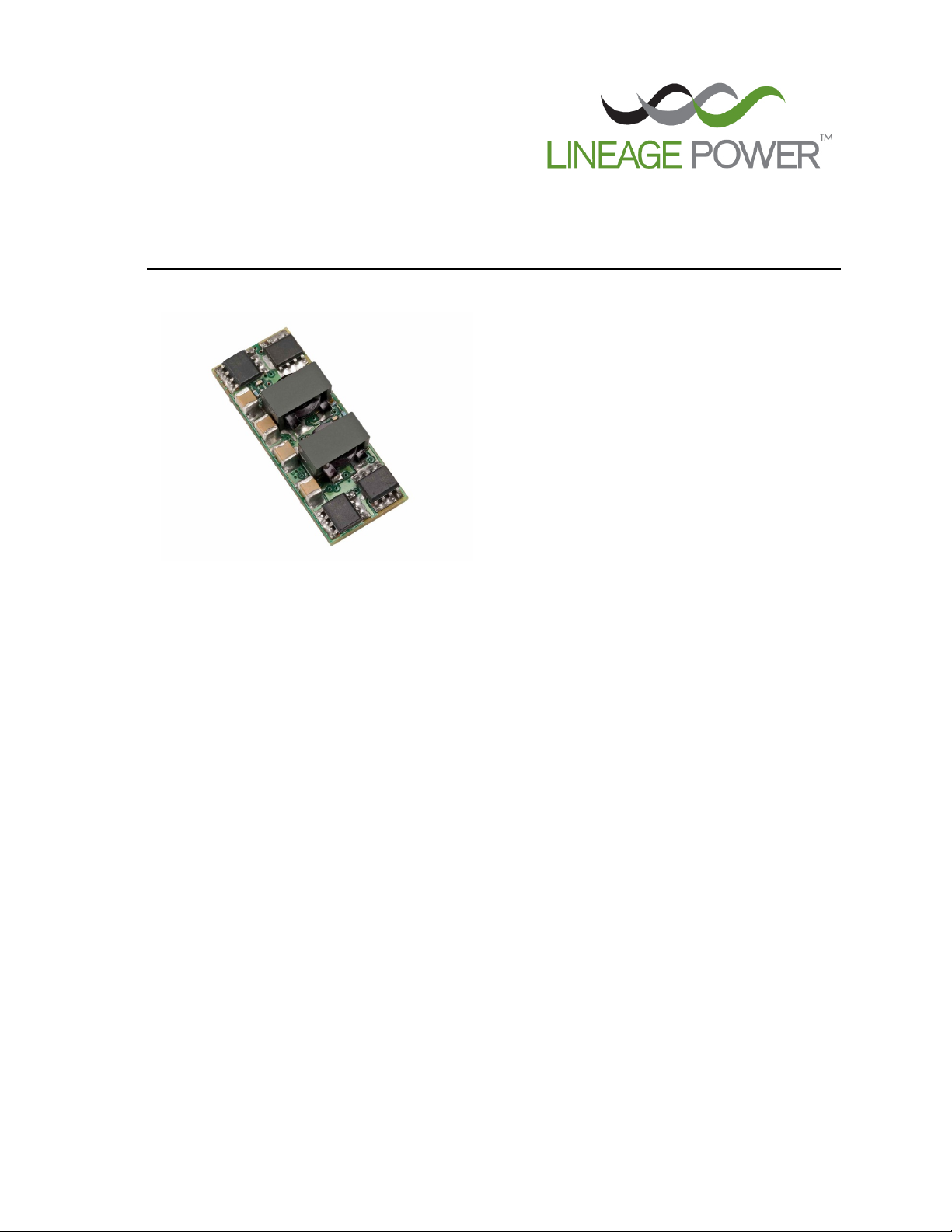
Austin MegaLynx
TM
SMT: Non-Isolated DC-DC Power Modules:
4.5Vdc – 5.5Vdc input; 0.8 to 3.63Vdc; 30A Output Current
6.0Vdc – 14Vdc input; 0.8 to 3.63Vdc Output; 20/30A Output Current
RoHS Compliant
Applications
Distributed power architectures
Intermediate bus voltage applications
Telecommunications equipment
Servers and storage applications
Networking equipment
Features
Compliant to RoHS EU Directive 2002/95/EC (-Z
versions)
Compliant to ROHS EU Directive 2002/95/EC with
lead solder exemption (non-Z versions)
Delivers up to 30A of output current
High efficiency: 92% @ 3.3V full load (12Vin)
Available in two input voltage ranges
ATH: 4.5 to 5.5Vdc
ATS: 6 to 14Vdc
• Output voltage programmable from
ATH: 0.8 to 3.63Vdc
ATS030: 0.8 to 2.75Vdc
ATS020: 0.8 to 3.63Vdc
Small size and low profile:
33.0 mm x 10.0 mm x 13.5 mm
(1.30 in. x 0.39 in. x 0.53 in.)
Monotonic start-up into pre-biased output
Output voltage sequencing (EZ-SEQUENCE
Remote On/Off
Remote Sense
Over current and Over temperature protection
-P option: Paralleling with active current share
-H option: Additional GND pins for improved
thermal derating
Wide operating temperature range (-40°C to 85°C)
UL* 60950 Recognized, CSA
60950-00 Certified, and VDE
rd
3
edition) Licensed
ISO** 9001 and ISO 14001 certified
manufacturing facilities
†
C22.2 No.
‡
0805 (EN60950-1
TM
)
Description
The Austin MegaLynx series SMT power modules are non-isolated DC-DC converters in an industry standard
package that can deliver up to 30A of output current with a full load efficiency of 92% at 2.5Vdc output voltage (V
12Vdc). The ATH series of modules operate off an input voltage from 4.5 to 5.5Vdc and provide an output voltage
that is programmable from 0.8 to 3.63Vdc, while the ATS series of modules have an input voltage range from 6 to
14V and provide a programmable output voltage ranging from 0.8 to 3.63Vdc. Both series have a sequencing
feature that enables designers to implement various types of output voltage sequencing when powering multiple
modules on the board. Additional features include remote On/Off, adjustable output voltage, remote sense, over
current, over temperature protection and active current sharing between modules.
* UL is a re gistered trademark of Underwriters Laboratories, Inc.
†
CSA is a reg istered trademark of Canadian Standards Associat ion.
‡
VDE is a t rademark of Verband Deutscher Elektrotechniker e.V.
** ISO is a registered trademark of the International Orga nization of Standards
Document No: DS06-109 ver. 1.15
PDF Name: austin_megalynx_smt.pdf
IN
=
Page 2
Data Sheet
September 10, 2013
Austin MegaLynx
4.5 – 5.5Vdc input; 0.8 to 3.63Vdc Output; 30A output current
TM
SMT: Non-Isolated DC-DC Power Modules:
6.0 – 14Vdc Input; 0.8Vdc to 3.63Vdc Output; 20/30A output
Absolute Maximum Ratings
Stresses in excess of the absolute maximum ratings can cause permanent damage to the device. These are
absolute stress ratings only, functional operation of the device is not implied at these or any other conditions in
excess of those given in the operations sections of the data sheet. Exposure to absolute maximum ratings for
extended periods can adversely affect the device reliability.
Parameter Device Symbol Min Max Unit
Input Voltage
Continuous ATH V
ATS V
IN
IN
-0.3 6 Vdc
-0.3 15 Vdc
Sequencing pin voltage ATH VsEQ -0.3 6 Vdc
ATS VsEQ -0.3 15 Vdc
Operating Ambient Temperature All T
A
-40 85 °C
(see Thermal Considerations section)
Storage Temperature All T
stg
-55 125 °C
Electrical Specifications
Unless otherwise indicated, specifications apply over all operating input voltage, resistive load, and temperature
conditions.
Parameter Device Symbol Min Typ Max Unit
Operating Input Voltage ATH VIN 4.5 5.0 5.5 Vdc
ATS VIN 6.0 12 14 Vdc
Maximum Input Current ATH I
(VIN= V
IN,min
, VO= V
O,set, IO=IO, max
) ATS020 I
ATS030 I
Inrush Transient All
IN,max
IN,max
IN,max
2
I
t
Input Reflected Ripple Current, peak-topeak
(5Hz to 20MHz, 1μH source impedance;
V
=6.0V to 14.0V, IO= I
IN
; See Figure 1)
Omax
All 100 mAp-p
Input Ripple Rejection (120Hz) All 50 dB
27 Adc
13.3 Adc
15.8 Adc
1
2
A
s
LINEAGE POWER 2
Page 3

Data Sheet
September 10, 2013
Austin MegaLynx
4.5 – 5.5Vdc input; 0.8 to 3.63Vdc Output; 30A output current
TM
SMT: Non-Isolated DC-DC Power Modules:
6.0 – 14Vdc Input; 0.8Vdc to 3.63Vdc Output; 20/30A output
Electrical Specifications (continued)
Parameter Device Symbol Min Typ Max Unit
Output Voltage Set-point All V
(VIN=V
IN,nom
, IO=I
, T
=25°C)
O, nom
ref
Output Voltage
(Over all operating input voltage, resistive load,
and temperature conditions until end of life)
All V
Adjustment Range
O, set
O, set
Selected by an external resistor ATS030 0.8 2.75 Vdc
ATS020 0.8 3.63 Vdc
ATH030* 0.8 3.63 Vdc
* VO ≥ 3.3V only possible for V
≥ 4.75V
IN
Output Regulation
Line (VIN=V
Load (IO=I
IN, min
O, min
to V
to I
) All
IN, max
) All
O, max
(-P version)
Temperature (T
ref=TA, min
to T
) All ⎯ 0.5 1 % V
A, max
Output Ripple and Noise on nominal output
(VIN=V
C
OUT
IN, nom
and IO=I
O, min
to I
O, max
= 0.1μF // 10 μF ceramic capacitors)
Peak-to-Peak (5Hz to 20MHz bandwidth) Vo ≤ 2.5V
Peak-to-Peak (5Hz to 20MHz bandwidth) 2.5V < Vo ≤ 3.63V
Peak-to-Peak (5Hz to 20MHz bandwidth) Vo > 3.63V
External Capacitance 1
ESR ≥ 1 mΩ All C
ESR ≥ 10 mΩ All C
Output Current
(VIN = 4.5 to 5.5Vdc) ATH Series I
(VIN = 6 to 14Vdc) ATS030 Series I
(VIN = 6 to 14Vdc) ATS020 Series I
Output Current Limit Inception (Hiccup Mode) All I
Output Short-Circuit Current All I
(VO≤250mV) ( Hiccup Mode )
Efficiency V
ATH Series: VIN=5Vdc, TA=25°C V
IO=I
O, max , VO
= V
V
O,set
V
V
V
ATS Series: VIN=12Vdc, TA=25°C V
IO=I
O, max , VO
= V
V
O,set
V
= 0.8dc η
O,set
= 1.2Vdc η
O,set
= 1.5Vdc η
O,set
= 1.8Vdc η
O,set
= 2.5Vdc η
O,set
= 3.3Vdc η
O,set
= 0.8dc η 77.5 %
O,set
= 1.2Vdc η 83.5 %
O,set
= 1.8Vdc η 86.5 %
O,set
O, max
O, max
o
o
o
O, lim
O, s/c
-1.5
⎯
–5.0
⎯
⎯ ⎯
⎯ ⎯
⎯ ⎯
⎯
⎯
⎯
50 mV
75 mV
100 mV
+1.5 % V
+3.0 % V
O, set
O, set
20 mV
40 mV
70 mV
O, set
pk-pk
pk-pk
pk-pk
0
0
⎯
⎯
2,000 μF
10,000 μF
0 30 Adc
0 30 Adc
0 20 Adc
⎯
⎯
140
3.5
⎯
⎯
% I
omax
Adc
82.2
85.8
89.5
89.2
92.0
92.2
%
%
%
%
%
%
1
Note that maximum external capacitance may be lower when sequencing is employed. Please check with your Lineage Power
Technical representative.
LINEAGE POWER 3
Page 4

Data Sheet
September 10, 2013
Austin MegaLynx
4.5 – 5.5Vdc input; 0.8 to 3.63Vdc Output; 30A output current
TM
SMT: Non-Isolated DC-DC Power Modules:
6.0 – 14Vdc Input; 0.8Vdc to 3.63Vdc Output; 20/30A output
V
V
Switching Frequency, Fixed All f
= 2.5Vdc η 91.3 %
O,set
= 3.3Vdc η 92.1 %
O,set
sw
⎯
300
⎯
kHz
LINEAGE POWER 4
Page 5
Data Sheet
September 10, 2013
Austin MegaLynx
4.5 – 5.5Vdc input; 0.8 to 3.63Vdc Output; 30A output current
TM
SMT: Non-Isolated DC-DC Power Modules:
6.0 – 14Vdc Input; 0.8Vdc to 3.63Vdc Output; 20/30A output
Electrical Specifications (continued)
Parameter Device Symbol Min Typ Max Unit
Dynamic Load Response
(dIO/dt=5A/μs; VIN=12V, Vo=3.3V ; TA=25°C)
Load Change from Io= 50% to 100% of IO,max;
No external output capacitors
Peak Deviation All V
Settling Time (VO<10% peak deviation)
(dIO/dt=5A/μs; VIN=VIN,
; TA=25°C)
nom
Load Change from IO= 100% to 50%of IO,
No external output capacitors
max
:
All t
Peak Deviation All V
Settling Time (VO<10% peak deviation)
(dIO/dt=5A/μs; VIN=VIN,
; TA=25°C)
nom
Load Change from Io= 50% to 100% of Io,max;
2x150 μF polymer capacitor
All t
Peak Deviation All V
Settling Time (VO<10% peak deviation)
(dIO/dt=5A/μs; VIN=VIN,
; TA=25°C)
nom
Load Change from Io= 100% to 50%of I
2x150 μF polymer capacitor
O,max
:
All t
Peak Deviation All V
Settling Time (VO<10% peak deviation)
All t
pk
s
pk
s
pk
s
pk
s
⎯
⎯
350 mV
25
⎯ μs
⎯
⎯
350 mV
25
⎯ μs
⎯
⎯
250
40
⎯
⎯ μs
⎯
⎯
250
40
⎯
⎯ μs
mV
mV
General Specifications
Parameter Min Typ Max Unit
Calculated MTBF (VIN=12V, VO=3.3Vdc, IO= 0.8I
T
=40°C) Per Telecordia Method
A
Weight
O, max
,
⎯
3,016,040
6.2 (0.22)
Hours
⎯
g (oz.)
LINEAGE POWER 5
Page 6
Data Sheet
September 10, 2013
Austin MegaLynx
4.5 – 5.5Vdc input; 0.8 to 3.63Vdc Output; 30A output current
TM
SMT: Non-Isolated DC-DC Power Modules:
6.0 – 14Vdc Input; 0.8Vdc to 3.63Vdc Output; 20/30A output
Feature Specifications
Unless otherwise indicated, specifications apply over all operating input voltage, resistive load, and temperature
conditions. See Feature Descriptions for additional information.
Parameter Device Symbol Min Typ Max Unit
On/Off Signal Interface
(VIN=V
Signal referenced to GND)
Logic High (Module OFF)
Input High Current All IIH
Input High Voltage All VIH
Logic Low (Module ON)
Input Low Current All IIL
Input Low Voltage All VIL
Turn-On Delay and Rise Times
IN, min
to V
; open collector or equivalent,
IN, max
0.5
3.0
⎯
⎯
3.3 mA
V
IN, max
⎯ ⎯
-0.3
200 µA
⎯
1.2 V
V
(VIN=V
Case 1: On/Off input is enabled and then
IN, nom
, IO=I
to within ±1% of steady state)
O, max , VO
All Tdelay ― 2.5 5 msec
input power is applied (delay from instant at
which V
Case 2: Input power is applied for at least one second and
IN
= V
until Vo = 10% of Vo, set)
IN, min
All Tdelay ― 2.5 5 msec
then the On/Off input is enabled (delay from instant at which
Von/Off is enabled until V
Output voltage Rise time (time for Vo to rise from
o = 10% of Vo, set)
All Trise
2 10 msec
10% of Vo, set to 90% of Vo, set)
Output voltage overshoot 3.0 % V
IO = I
Remote Sense Range All
Over temperature Protection All T
(See Thermal Consideration section)
O, max
; V
IN, min
– V
, TA = 25 oC
IN, max
ref
⎯ ⎯
125
⎯
0.5 V
⎯
°C
O, set
Sequencing Slew rate capability All dVSEQ/dt — 2 V/msec
(V
to V
IN, min
Sequencing Delay time (Delay from V
IN, max
; I
to I
O, min
VSEQ < Vo)
O, max
IN, min
to application of voltage on SEQ pin) All TsEQ-delay 10 msec
Tracking Accuracy Power-up (2V/ms) All VSEQ –Vo 100 200 mV
Power-down (1V/ms) VSEQ –Vo 200 400 mV
(V
to V
IN, min
Input Undervoltage Lockout
Turn-on Threshold ATH
Turn-off Threshold ATH
Turn-on Threshold ATS
Turn-off Threshold ATS
Forced Load Share Accuracy -P
Number of units in Parallel -P
IN, max
; I
- I
O, min
VSEQ < Vo)
O, max
4.3 Vdc
3.9 Vdc
5.5 Vdc
5.0 Vdc
10 % Io
⎯
5
LINEAGE POWER 6
Page 7
TM
Data Sheet
September 10, 2013
Austin MegaLynx
4.5 – 5.5Vdc input; 0.8 to 3.63Vdc Output; 30A output current
SMT: Non-Isolated DC-DC Power Modules:
6.0 – 14Vdc Input; 0.8Vdc to 3.63Vdc Output; 20/30A output
Characteristic Curves
The following figures provide typical characteristics for the ATS030A0X3-SR & -SRH (0.8V, 30A) at 25oC.
90
Vin = 6 V
85
80
Vin = 12 V
75
Vin = 14 V
EFFICIENCY, η (%)
70
0 5 10 15 20 25 30
OUTPUT CURRENT, IO (A) AMBIENT TEMPERATURE, TA OC
Figure 1. Converter Efficiency versus Output Current.
(V) (20mV/div)
O
V
OUTPUT VOLTAGE
TIME, t (1μs/div)
Figure 2. Typical output ripple and noise (V
o
= I
o,max
I
).
IN
= V
IN,NOM
,
35
30
25
20
15
10
5
0
OUTPUT CURRENT, Io (A)
35 45 55 65 75 85
0.5m/s
(100LFM)
(200LFM)
1m/s
1.5m/s
(300LFM)
(400LFM)
Figure 4. Derating Output Current versus Ambient
Temperature and Airflow (ATS030A0X3-SRH).
35
30
25
20
15
10
5
0
OUTPUT CURRENT, Io (A)
35 45 55 65 75 85
0.5m/s
NC
(100LFM)
1m/s
(200LFM)
1.5m/s
(300LFM)
2m/s
(400LFM)
2.5m/s
(500LFM)
AMBIENT TEMPERATURE, T
Figure 5. Derating Output Current versus Ambient
Temperature and Airflow (ATS030A0X3-SR).
2.0m/s
OC
A
2.5m/s
(500LFM)
(V) (100mV/div)
O
(A) (5Adiv) V
O
OUTPUT CURRENT, OUTPUT VOLTAGE
I
TIME, t (20μs /div)
Figure 3. Transient Response to Dynamic Load Change
from 0% to 50% to 0% of full load with V
=12V.
IN
(V) (0.5V/div)
O
(V) (5V/div) V
IN
INPUT VOLTAGE OUTPUT VOLTAGE
V
TIME, t (5ms/div)
Figure 6. Typical Start-up Using Input Voltage (V
IN,NOM
, Io = I
o,max
V
).
IN
=
LINEAGE POWER 7
Page 8
Data Sheet
September 10, 2013
Austin MegaLynx
4.5 – 5.5Vdc input; 0.8 to 3.63Vdc Output; 30A output current
TM
SMT: Non-Isolated DC-DC Power Modules:
6.0 – 14Vdc Input; 0.8Vdc to 3.63Vdc Output; 20/30A output
Characteristic Curves
The following figures provide typical characteristics for the ATS030A0X3-SR and -SRH (1.25V, 30A) at 25oC.
95
Vin = 6 V
90
85
80
75
Vin = 12 V
Vin = 14 V
EFFICIENCY, η (%)
70
0 5 10 15 20 25 30
OUTPUT CURRENT, IO (A)
Figure 7. Converter Efficiency versus Output Current.
35
30
25
20
15
10
5
0
OUTPUT CURRENT, Io (A)
35 45 55 65 75 85
0.5m/s
(100LFM)
1m/s
(200LFM)
1.5m/s
(300LFM)
2.0m/s
(400LFM)
(500LFM)
2.5m/s
AMBIENT TEMPERATURE, TA OC
Figure 8. Derating Output Current versus Ambient
Temperature and Airflow (ATS030A0X3-SRH).
35
30
25
20
15
10
5
0
OUTPUT CURRENT, Io (A)
35 45 55 65 75 85
0.5m/s
NC
(100LFM)
(200LFM)
1m/s
1.5m/s
(300LFM)
(400LFM)
AMBIENT TEMPERATURE, TA OC
2m/s
2.5m/s
(500LFM)
Figure 9. Derating Output Current versus Ambient
Temperature and Airflow (ATS030A0X3-SR).
LINEAGE POWER 8
Page 9
TM
OUTPUT
CURRENT
OUTPUT
VOLTAGE
Data Sheet
September 10, 2013
Austin MegaLynx
4.5 – 5.5Vdc input; 0.8 to 3.63Vdc Output; 30A output current
SMT: Non-Isolated DC-DC Power Modules:
6.0 – 14Vdc Input; 0.8Vdc to 3.63Vdc Output; 20/30A output
Characteristic Curves
The following figures provide typical characteristics for the ATS030A0X3-SR and –SRH (1.8V, 30A) at 25oC.
95
Vin = 6 V
90
85
Vin = 12 V
80
75
Vin = 14 V
EFFICIENCY, η (%)
70
0 5 10 15 20 25 30
OUTPUT CURRENT, IO (A) AMBIENT TEMPERATURE, TA OC
Figure 10. Converter Efficiency versus Output
Current.
OUTPUT VOLTAGE
(V) (20mV/div)
O
V
TIME, t (1μs/div)
Figure 11. Typical output ripple and noise (V
V
IN,NOM
, Io = I
o,max
).
IN
=
35
30
25
20
15
10
OUTPUT CURRENT, Io (A)
0.5m/s
(100LFM)
5
0
35 45 55 65 75 85
1m/s
(200LFM)
1.5m/s
(300LFM)
2m/s
(400LFM)
Figure 13. Output Current Derating versus Ambient
Temperature and Airflow (ATS030A0X3-SRH).
35
30
25
20
15
10
5
0
OUTPUT CURRENT, Io (A)
35 45 55 65 75 85
NC
0.5m/s
(100LFM)
(200LFM)
1m/s
1.5m/s
(300LFM)
2m/s
(400LFM)
(500LFM)
2.5m/s
AMBIENT TEMPERATURE, T
Figure 14. Output Current Derating versus Ambient
Temperature and Airflow (ATS030A0X3-SR).
A
OC
2.5m/s
(500 LFM)
(V) (100mV/div)
O
,
(A) (5A/div) V
O
I
TIME, t (20μs /div)
Figure 12. Transient Response to Dynamic Load
Change from 0% to 50% to 0% of full load with V
=12V.
IN
(V) (1V/div)
O
(V) (5V/div) V
IN
INPUT VOLTAGE OUTPUT VOLTAGE
V
TIME, t (5ms/div)
Figure 15. Typical Start-up Using Input Voltage (V
IN,NOM
, Io = I
o,max
V
).
IN
=
LINEAGE POWER 9
Page 10

Data Sheet
September 10, 2013
Austin MegaLynx
4.5 – 5.5Vdc input; 0.8 to 3.63Vdc Output; 30A output current
TM
SMT: Non-Isolated DC-DC Power Modules:
6.0 – 14Vdc Input; 0.8Vdc to 3.63Vdc Output; 20/30A output
Characteristic Curves
The following figures provide typical characteristics for the ATS030A0X3-SR and -SRH (2.5V, 30A) at 25oC.
100
95
90
85
Vin = 6 V
80
75
Vin = 12 V
EFFICIENCY, η (%)
70
0 5 10 15 20 25 30
Vin = 14 V
OUTPUT CURRENT, IO (A)
Figure 16. Converter Efficiency versus Output Current.
35
30
25
20
15
NC
10
5
0
OUTPUT CURRENT, Io (A)
35 45 55 65 75 85
0.5m/s
(100LFM)
(200LFM)
1m/s
1.5m/s
(300LFM)
2m/s
(400LFM)
2.5m/s
(500LFM)
AMBIENT TEMPERATURE, TA OC
Figure 17. Derating Output Current versus Ambient
Temperature and Airflow (ATS030A0X3-SRH).
30
25
20
15
10
5
0
OUTPUT CURRENT, Io (A)
35 45 55 65 75 85
0.5m/s
(100LFM)
NC
1m/s
(200LFM)
1.5m/s
(300LFM)
2m/s
(400LFM)
AMBIENT TEMPERATURE, TA OC
2.5m/s
(500LFM)
Figure 18. Derating Output Current versus Ambient
Temperature and Airflow (ATS030A0X3-SR).
LINEAGE POWER 10
Page 11

Data Sheet
OUTPUT
CURRENT
OUTPUT
VOLTAGE
September 10, 2013
Austin MegaLynx
4.5 – 5.5Vdc input; 0.8 to 3.63Vdc Output; 30A output current
TM
SMT: Non-Isolated DC-DC Power Modules:
6.0 – 14Vdc Input; 0.8Vdc to 3.63Vdc Output; 20/30A output
Characteristic Curves
The following figures provide typical characteristics for the ATS020A0X3-SR and –SRH (3.3V, 20A) at 25oC.
100
25
95
90
85
80
75
EFFICIENCY, η (%)
70
0 5 10 15 20
Vin = 12 V
Vin = 6 V
Vin = 14 V
OUTPUT CURRENT, IO (A) AMBIENT TEMPERATURE, TA OC
Figure 19. Converter Efficiency versus Output
Current.
OUTPUT VOLTAGE
Figure 20. Typical output ripple and noise (V
V
(V) (20mV/div)
O
V
IN,NOM, Io = Io,max).
TIME, t (1μs/div)
IN =
20
15
10
OUTPUT CURRENT, Io (A)
NC
5
0
30 40 50 60 70 80
0.5m/s
(100LFM)
1m/s
(200LFM)
1.5m/s
(300LFM)
2m/s
(400LFM)
(500LFM)
Figure 22. Output Current Derating versus Ambient
Temperature and Airflow (ATS020A0X3-SRH).
25
20
15
10
5
0
OUTPUT CURRENT, Io (A)
30 40 50 60 70 80
0.5m/s
NC
(100L FM)
(200LFM)
1m/s
1.5m/s
(300L FM)
AMBIENT TEMPERATURE, T
2m/s
(400LFM)
(500 LFM)
2.5m/s
A
OC
Figure 23. Output Current Derating versus Ambient
Temperature and Airflow (ATS020A0X3-SR).
2.5m/s
(V) (100mV/div)
O
,
(A) (5A/div) V
O
I
TIME, t (20μs /div)
Figure 21. Transient Response to Dynamic Load
Change from 0% to 50% of full load with V
LINEAGE POWER 11
=12V.
IN
(V) (1V/div)
O
(V) (5V/div) V
IN
INPUT VOLTAGE OUTPUT VOLTAGE
V
TIME, t (5ms/div)
Figure 24. Typical Start-up Using Input Voltage (V
V
IN,NOM, Io = Io,max).
IN =
Page 12

Data Sheet
September 10, 2013
Austin MegaLynx
4.5 – 5.5Vdc input; 0.8 to 3.63Vdc Output; 30A output current
TM
SMT: Non-Isolated DC-DC Power Modules:
6.0 – 14Vdc Input; 0.8Vdc to 3.63Vdc Output; 20/30A output
Characteristic Curves
The following figures provide typical characteristics for the ATH030A0X3-SR and –SRH (0.8V, 30A) at 25oC.
95
90
85
80
EFFICIENCY, η (%)
Vin = 5.5 V
75
0 5 10 15 20 25 30
Vin = 4.5 V
Vin = 5.0 V
OUTPUT CURRENT, IO (A) AMBIENT TEMPERATURE, TA OC
Figure 25. Converter Efficiency versus Output
Current.
Figure 26. Typical output ripple and noise (V
V
(V) (20mV/div)
O
V
OUTPUT VOLTAGE
IN,NOM, Io = Io,max).
TIME, t (1μs/div)
IN =
35
30
25
20
15
10
5
0
OUTPUT CURRENT, Io (A)
35 45 55 65 75 85
0.5m/s
(100LFM)
(200LFM)
1m/s
1.5m/s
(300LFM)
(400LFM)
2.0m/s
Figure 28. Derating Output Current versus Ambient
Temperature and Airflow (ATS030A0X3-SRH).
35
30
25
20
15
10
5
0
OUTPUT CURRENT, Io (A)
35 45 55 65 75 85
AMBIENT TEMPERATURE, T
0.5m/s
(100LFM)
(200LFM)
1m/s
1.5m/s
(300LFM)
(400LFM)
2.0m/s
OC
A
Figure 29. Derating Output Current versus Ambient
Temperature and Airflow (ATH030A0X3-SR).
2.5m/s
(500LFM)
2.5m/s
(500LFM)
(V) (1V/div)
O
(V) (100mV/div)
O
(V) (2V/div) V
IN
V
(A) (5A/div) V
O
OUTPUT CURRENT, OUTPUT VOLTAGE
I
TIME, t (10μs /div)
Figure 27. Transient Response to Dynamic Load
Change from 0% to 50% of full load with V
IN
=5V.
INPUT VOLTAGE OUTPUT VOLTAGE
TIME, t (2ms/div)
Figure 30. Typical Start-up Using Input Voltage (V
V
IN,NOM, Io = Io,max).
IN =
LINEAGE POWER 12
Page 13

Data Sheet
September 10, 2013
Austin MegaLynx
4.5 – 5.5Vdc input; 0.8 to 3.63Vdc Output; 30A output current
TM
SMT: Non-Isolated DC-DC Power Modules:
6.0 – 14Vdc Input; 0.8Vdc to 3.63Vdc Output; 20/30A output
Characteristic Curves
The following figures provide typical characteristics for the ATH030A0X3-SR and –SRH (1.8V, 30A) at 25oC.
95
90
85
80
Vin = 4.5 V
Vin = 5.0 V
Vin = 5.5 V
EFFICIENCY, η (%)
75
0 5 10 15 20 25 30
OUTPUT CURRENT, IO (A) AMBIENT TEMPERATURE, TA OC
Figure 31. Converter Efficiency versus Output
Current.
(V) (20mV/div)
O
V
OUTPUT VOLTAGE
TIME, t (1μs/div)
Figure 32. Typical output ripple and noise (VIN =
V
IN,NOM, Io = Io,max).
35
30
25
20
15
10
5
0
OUTPUT CURRENT, Io (A)
35 45 55 65 75 85
0.5m/s
100LFM
1m/s
200LFM
1.5m/s
300LFM
400LFM
Figure 34. Derating Output Current versus Ambient
Temperature and Airflow (ATH030A0X3-SRH).
35
30
25
20
15
10
5
0
OUTPUT CURRENT, Io (A)
35 45 55 65 75 85
0.5m/s
(100LFM)
1m/s
(200LFM)
1.5m/s
(300LFM)
(400LFM)
AMBIENT TEMPERATURE, T
2m/s
A
OC
Figure 35. Derating Output Current versus Ambient
Temperature and Airflow (ATH030A0X3-SR).
2m/s
(500LFM)
2.5m/s
500LFM
2.5m/s
(V) (0.5V/div)
O
(V) (100mV/div)
O
(V) (2V/div) V
IN
(A) (5A/div) V
O
OUTPUT CURRENT, OUTPUT VOLTAGE
I
TIME, t (10μs /div)
Figure 33. Transient Response to Dynamic Load
Change from 0% to 50% of full load with V
IN
=5V.
INPUT VOLTAGE OUTPUT VOLTAGE
V
TIME, t (2ms/div)
Figure 36. Typical Start-up Using Input Voltage (V
V
IN,NOM, Io = Io,max).
IN =
LINEAGE POWER 13
Page 14

Data Sheet
September 10, 2013
Austin MegaLynx
4.5 – 5.5Vdc input; 0.8 to 3.63Vdc Output; 30A output current
TM
SMT: Non-Isolated DC-DC Power Modules:
6.0 – 14Vdc Input; 0.8Vdc to 3.63Vdc Output; 20/30A output
Characteristic Curves
The following figures provide typical characteristics for the ATH030A0X3-SR and –SRH (3.3V, 30A) at 25oC.
100
95
90
85
80
Vin = 4.5 V
Vin = 5.0 V
Vin = 5.5 V
EFFICIENCY, η (%)
75
0 5 10 15 20 25 30
OUTPUT CURRENT, IO (A) AMBIENT TEMPERATURE, TA OC
Figure 37. Converter Efficiency versus Output
Current.
Figure 38. Typical output ripple and noise (V
V
(V) (20mV/div)
O
V
OUTPUT VOLTAGE
IN,NOM, Io = Io,max).
TIME, t (1μs/div)
IN =
35
30
25
20
15
10
5
0
OUTPUT CURRENT, Io (A)
35 45 55 65 75 85
0.5m/s
(100LFM)
1m/s
(200LFM)
1.5m/s
(300LFM)
2m/s
(400LFM)
Figure 40. Derating Output Current versus Ambient
Temperature and Airflow (ATH030A0X3-SRH).
35
30
25
20
15
10
5
0
OUTPUT CURRENT, Io (A)
35 45 55 65 75 85
0.5m/s
100LFM
1m/s
200LFM
1.5m/s
300LFM
AMBIENT TEMPERATURE, T
2m/s
400LFM
OC
A
Figure 41. Derating Output Current versus Ambient
Temperature and Airflow (ATH030A0X3-SR).
2.5m/s
(500LFM)
2.5m/s
500LFM
(V) (1V/div)
(V) (100mV/div)
O
(A) (10A/div) V
O
OUTPUT CURRENT, OUTPUT VOLTAGE
I
TIME, t (10μs /div)
Figure 39. Transient Response to Dynamic Load
Change from 0% to 50% of full load with V
IN
=5V.
O
(V) (2V/div) V
IN
INPUT VOLTAGE OUTPUT VOLTAGE
V
TIME, t (2ms/div)
Figure 42. Typical Start-up Using Input Voltage (V
V
IN,NOM, Io = Io,max).
IN =
LINEAGE POWER 14
Page 15

Data Sheet
p
pp
g
(
p
p)
p
pp
g
(
p
p)
F
F
F
F
September 10, 2013
Austin MegaLynx
TM
SMT: Non-Isolated DC-DC Power Modules:
4.5 – 5.5Vdc input; 0.8 to 3.63Vdc Output; 30A output current
6.0 – 14Vdc Input; 0.8Vdc to 3.63Vdc Output; 20/30A output
Test Configurations
TO OSCILLOSCOPE
L
TEST
1μH
CS 220μF
BATTERY
E.S.R.<0.1Ω
@ 20°C 100kHz
CURRENT PROBE
CIN
Min
150μF
VIN(+)
COM
Design Considerations
The Austin MegaLynxTM module should be
connected to a low-impedance source. A highly
inductive source can affect the stability of the
module. An input capacitor must be placed directly
adjacent to the input pin of the module, to minimize
input ripple voltage and ensure module stability.
To minimize input voltage ripple, low-ESR ceramic
capacitors are recommended at the input of the
module. Figure 46 shows the input ripple voltage for
various output voltages at 30A of load current with
1x22 µF or 2x22 µF ceramic capacitors and an
input of 12V. Figure 47 shows data for the 5Vin
NOTE: Measure input reflected ripple current with a simulated
source indu ctance (L
possibl e batter y impedance. M easure cur rent as shown
above.
) of 1μH. Capacitor CS offsets
TEST
Figure 43. Input Reflected Ripple Current Test
Setup.
COPPER STRIP
V
(+)
O
1uF .
COM
NOTE: All voltage measurements to be taken at the module
terminals, as shown above. If sockets are used then
Kelvin connections are required at the module terminals
to avoid measurement errors due to socket contact
resistance.
10uF
GROUND PLANE
SCOPE
RESISTIVE
LOAD
Figure 44. Output Ripple and Noise Test Setup.
R
R
contact
distribution
V
R
R
contact
distribution
NOTE: All volt age meas urements to be taken at th e module
terminals , as shown above. If sock ets are us ed then
Kelvin conn ections are requir ed at the modu le termi nals
to avoid measur ement err ors due to soc ket contact
resistance.
IN
VIN(+)
COM
V
COM
R
O
contactRdistribution
R
R
contactRdistribution
LOAD
V
O
Figure 45. Output Voltage and Efficiency Test
Setup.
. I
V
O
VIN. I
O
IN
x 100 %
Efficiency
=
η
LINEAGE POWER 15
case, with 2x22µF and 2x47µF of ceramic
capacitors at the input, and for a load current of
30A.
350
-
mV
e
300
250
200
1 x 22u
2 x 22u
150
le Volta
100
50
ut Ri
0
In
0.5 1 1.5 2 2.5
Output Voltage (Vdc)
Figure 46. Input ripple voltage for various
output voltages with 1x22 µF or 2x22 µF ceramic
capacitors at the input (30A load). Input voltage
is 12V.
120
-
100
mV
80
e
60
40
le Volta
20
ut Ri
0
In
0.5 1 1.5 2 2.5 3 3.5
2 x 22u
2 x 47u
Output Voltage (Vdc)
Figure 47. Input ripple voltage in mV, p-p for
various output voltages with 2x22 µF or 2x47 µF
ceramic capacitors at the input (30A load). Input
voltage is 5V.
Page 16

Data Sheet
September 10, 2013
Austin MegaLynx
4.5 – 5.5Vdc input; 0.8 to 3.63Vdc Output; 30A output current
6.0 – 14Vdc Input; 0.8Vdc to 3.63Vdc Output; 20/30A output
Output Filtering
The Austin MegaLynxTM modules are designed for
low output ripple voltage and will meet the
maximum output ripple specification with 0.1 µF
ceramic and 10 µF ceramic capacitors at the output
of the module. However, additional output filtering
may be required by the system designer for a
number of reasons. First, there may be a need to
further reduce the output ripple and noise of the
module. Second, the dynamic response
characteristics may need to be customized to a
particular load step change.
To reduce the output ripple and improve the
dynamic response to a step load change, additional
capacitance at the output can be used. Low ESR
polymer and ceramic capacitors are recommended
to improve the dynamic response of the module.
Figure 48 shows the output ripple voltage for
various output voltages at 30A of load current with
different external capacitance values and an input
of 12V. Figure 49 shows data for the 5Vin case for
various output voltages at 30A of load current with
different external capacitance values. For stable
operation of the module, limit the capacitance to
less than the maximum output capacitance as
specified in the electrical specification table.
110
100
90
80
70
60
50
40
Ripple(mVp-p)
30
20
10
0
0.5 1 1.5 2 2.5
Output Voltage(Volts)
Figure 48. Output ripple voltage for various
output voltages with external 1x10 µF, 1x47 µF,
2x47 µF or 4x47 µF ceramic capacitors at the
output (30A load). Input voltage is 12V.
1x10uF External Cap
1x47uF External Cap
2x47uF External Cap
4x47uF External Cap
TM
SMT: Non-Isolated DC-DC Power Modules:
25
1x10uF E xternal C ap
1x47uF E xternal C ap
2x47uF E xternal C ap
4x47uF E xternal C ap
15
Ripp le(mVp -p)
5
0.511.522.5
Output Voltage(Volts)
Figure 49. Output ripple voltage for various
output voltages with external 1x10 µF, 1x47 µF,
2x47 µF or 4x47 µF ceramic capacitors at the
output (30A load). Input voltage is 5V.
Safety Considerations
For safety agency approval the power module must
be installed in compliance with the spacing and
separation requirements of the end-use safety
agency standards, i.e., UL 60950, CSA C22.2 No.
60950-00, EN60950 (VDE 0850) (IEC60950, 3
edition) Licensed.
For the converter output to be considered meeting
the requirements of safety extra-low voltage
(SELV), the input must meet SELV requirements.
The power module has extra-low voltage (ELV)
outputs when all inputs are ELV.
rd
Feature Descriptions
Remote On/Off
The Austin MegaLynxTM SMT power modules
feature a On/Off pin for remote On/Off operation. If
not using the On/Off pin, connect the pin to ground
(the module will be ON). The On/Off signal (V
on/off
)
is referenced to ground. Circuit configuration for
remote On/Off operation of the module using the
On/Off pin is shown in Figure 50.
During a Logic High on the On/Off pin (transistor Q1
is OFF), the module remains OFF. The external
resistor R1 should be chosen to maintain 3.0V
minimum on the On/Off pin to ensure that the
module is OFF when transistor Q1 is in the OFF
state. Suitable values for R1 are 4.7K for input
voltage of 12V and 3K for 5Vin. During Logic-Low
when Q1 is turned ON, the module is turned ON.
The ATS030A0X3-62SRHZ and ATS030A0X3-
LINEAGE POWER 16
Page 17

Data Sheet
September 10, 2013
Austin MegaLynx
4.5 – 5.5Vdc input; 0.8 to 3.63Vdc Output; 30A output current
6.0 – 14Vdc Input; 0.8Vdc to 3.63Vdc Output; 20/30A output
62SRPHZ modules have a higher value resistor of
100K connected internally between the gate and
source of the internal FET used to control the PWM
Enable line.
The On/Off pin can also be used to synchronize the
output voltage start-up and shutdown of multiple
modules in parallel. By connecting On/Off pins of
multiple modules, the output start-up can be
synchronized (please refer to characterization
curves). When On/Off pins are connected together,
all modules will shutdown if any one of the modules
gets disabled due to undervoltage lockout or over
temperature protection
VIN+
R1
I
ON/OF F
GND
ON/OFF
V
ON/OFF
Q1
+
_
Figure 50. Remote On/Off Implementation
using ON/OFF .
Remote Sense
The Austin MegaLynxTM SMT power modules have
a Remote Sense feature to minimize the effects of
distribution losses by regulating the voltage at the
Remote Sense pin (See Figure 51). The voltage
between the Sense pin and Vo pin must not exceed
0.5V.
The amount of power delivered by the module is
defined as the output voltage multiplied by the
output current (Vo x Io). When using Remote
Sense, the output voltage of the module can
increase, which, if the same output is maintained,
increases the power output by the module. Make
sure that the maximum output power of the module
remains at or below the maximum rated power.
When the Remote Sense feature is not being used,
connect the Remote Sense pin to output of the
module.
.
MODULE
Ther m al SD
1K
10K
PWM Enable
100K
TM
SMT: Non-Isolated DC-DC Power Modules:
R
distribution
R
distribution
R
contact
R
contact
VIN(+)
COM
V
Sense
COM
R
O
contact Rdistribution
R
LOAD
R
contact Rdistribution
Figure 51. Effective Circuit Configuration for
Remote Sense operation.
Over Current Protection
To provide protection in a fault (output overload)
condition, the unit is equipped with internal
current-limiting circuitry and can endure current
limiting continuously. At the point of current-limit
inception, the unit enters hiccup mode. The unit
operates normally once the output current is
brought back into its specified range. The average
output current during hiccup is 10% I
O, max
.
Over Temperature Protection
To provide protection in a fault condition, the unit is
equipped with a thermal shutdown circuit. The unit
will shutdown if the overtemperature threshold of
o
125
C is exceeded at the thermal reference point
T
. The thermal shutdown is not intended as a
ref
guarantee that the unit will survive temperatures
beyond its rating. Once the unit goes into thermal
shutdown it will then wait to cool before attempting
to restart.
Input Under Voltage Lockout
At input voltages below the input undervoltage
lockout limit, the module operation is disabled. The
module will begin to operate at an input voltage
above the undervoltage lockout turn-on threshold.
Output Voltage Programming
The output voltage of the Austin MegaLynxTM can
be programmed to any voltage from 0.8dc to
3.63Vdc by connecting a resistor (shown as R
Figure 52) between Trim and GND pins of the
module. Without an external resistor between Trim
and GND pins, the output of the module will be
0.8Vdc. To calculate the value of the trim resistor,
R
for a desired output voltage, use the following
trim
equation:
= 100
R
trim
Vo
R
is the external resistor in Ω
trim
1200
−
80.0
Ω
−
trim
in
LINEAGE POWER 17
Page 18

Data Sheet
September 10, 2013
Austin MegaLynx
4.5 – 5.5Vdc input; 0.8 to 3.63Vdc Output; 30A output current
6.0 – 14Vdc Input; 0.8Vdc to 3.63Vdc Output; 20/30A output
Vo is the desired output voltage
By using a ±0.5% tolerance trim resistor with a TC
of ±100ppm, a set point tolerance of ±1.5% can be
achieved as specified in the electrical specification.
Table 1 provides Rtrim values required for some
common output voltages. The POL Programming
Tool, available at www.lineagepower.com under the
Design Tools section, helps determine the required
external trim resistor needed for a specific output
voltage.
V
V
(+)
IN
ON/OFF
GND
Figure 52. Circuit configuration to program
output voltage using an external resistor.
Voltage Margining
Output voltage margining can be implemented in
the Austin MegaLynx
resistor, R
pin for margining-up the output voltage and by
connecting a resistor, R
to output pin for margining-down. Figure 53 shows
the circuit configuration for output voltage
margining. The POL Programming Tool, available
at www.lineagepower.com under the Design Tools
section, also calculates the values of R
R
margin-down
margin. Please consult your local Lineage Power
technical representative for additional details.
margin-up
for a specific output voltage and %
(+)
O
TRIM
Rtrim
Table 1
V
(V)
O, set
0.8 Open
1.0 5.900
1.2 2.900
1.5 1.614
1.8 1.100
2.5 0.606
3.3 0.380
TM
, from the Trim pin to the ground
Rtrim (KΩ)
modules by connecting a
margin-down
, from the Trim pin
margin-up
LOAD
and
TM
SMT: Non-Isolated DC-DC Power Modules:
Vo
Rmargin-down
Austin Lynx or
Lynx II Series
Q2
Trim
Rmargin-up
Rtrim
Q1
GND
Figure 53. Circuit Configuration for margining
Output voltage.
Voltage Sequencing
The Austin MegaLynxTM series of modules include a
sequencing feature that enables users to implement
various types of output voltage sequencing in their
applications. This is accomplished via an additional
sequencing pin. When not using the sequencing
feature, either leave the SEQ pin unconnected or
tied to V
For proper voltage sequencing, first, input voltage is
applied to the module. The On/Off pin of the
module is or tied to GND so that the module is ON
by default. After applying input voltage to the
module, a delay of 10msec minimum is required
before applying voltage on the SEQ pin. During this
delay time, the SEQ pin should be kept at a voltage
of 50mV (± 20 mV). After the 10msec delay, the
voltage applied to the SEQ pin is allowed to vary
and the output voltage of the module will track this
voltage on a one-to-one volt basis until the output
reaches the set-point voltage. To initiate
simultaneous shutdown of the modules, the SEQ
pin voltage is lowered in a controlled manner. The
output voltages of the modules track the sequence
pin voltage when it falls below their set-point
voltages. A valid input voltage must be maintained
until the tracking and output voltages reach zero to
ensure a controlled shutdown of the modules. For a
more detailed description of sequencing, please
refer to Application Note AN04-008 titled
“Guidelines for Sequencing of Multiple
Modules”.
When using the EZ-SEQUENCE
control start-up of the module, pre-bias immunity
IN.
TM
feature to
LINEAGE POWER 18
Page 19

Data Sheet
September 10, 2013
Austin MegaLynx
4.5 – 5.5Vdc input; 0.8 to 3.63Vdc Output; 30A output current
6.0 – 14Vdc Input; 0.8Vdc to 3.63Vdc Output; 20/30A output
feature during start-up is disabled. The pre-bias
immunity feature of the module relies on the module
being in the diode-mode during start-up. When
using the EZ-SEQUENCE
through an internal set-up time of 10msec, and will
be in synchronous rectification mode when voltage
at the SEQ pin is applied. This will result in sinking
current in the module if pre-bias voltage is present
at the output of the module. When pre-bias
immunity during start-up is required, the EZSEQUENCE
TM
feature must be disabled.
Active Load Sharing (-P Option)
For additional power requirements, the Austin
MegaLynx series power module is also available
with a parallel option. Up to five modules can be
configured, in parallel, with active load sharing.
Good layout techniques should be observed when
using multiple units in parallel. To implement forced
load sharing, the following connections should be
made:
• The share pins of all units in parallel must be
connected together. The path of these
connections should be as direct as possible.
• All remote-sense pins should be connected to
the power bus at the same point, i.e., connect
all the SENSE
Close proximity and directness are necessary
for good noise immunity
Some special considerations apply for design of
converters in parallel operation:
• When sizing the number of modules required
for parallel operation, take note of the fact that
current sharing has some tolerance. In
addition, under transient condtions such as a
dynamic load change and during startup, all
converter output currents will not be equal. To
allow for such variation and avoid the likelihood
of a converter shutting off due to a current
overload, the total capacity of the paralleled
system should be no more than 75% of the
sum of the individual converters. As an
example, for a system of four ATS030A0X3-SR
converters the parallel, the total current drawn
should be less that 75% of (4 x 30A) , i.e. less
than 90A.
• All modules should be turned on and off
together. This is so that all modules come up at
the same time avoiding the problem of one
converter sourcing current into the other
leading to an overcurrent trip condition. To
ensure that all modules come up
simultaneously, the on/off pins of all paralleled
converters should be tied together and the
TM
feature, modules goes
(+) pins to the (+) side of the bus.
TM
SMT: Non-Isolated DC-DC Power Modules:
converters enabled and disabled using the
on/off pin.
• The share bus is not designed for redundant
operation and the system will be non-functional
upon failure of one of the unit when multiple
units are in parallel. In particular, if one of the
converters shuts down during operation, the
other converters may also shut down due to
their outputs hitting current limit. In such a
situation, unless a coordinated restart is
ensured, the system may never properly restart
since different converters will try to restart at
different times causing an overload condition
and subsequent shutdown. This situation can
be avoided by having an external output
voltage monitor circuit that detects a shutdown
condition and forces all converters to shut
down and restart together.
LINEAGE POWER 19
Page 20

Data Sheet
Air
W
September 10, 2013
Austin MegaLynx
4.5 – 5.5Vdc input; 0.8 to 3.63Vdc Output; 30A output current
6.0 – 14Vdc Input; 0.8Vdc to 3.63Vdc Output; 20/30A output
Thermal Considerations
Power modules operate in a variety of thermal
environments; however, sufficient cooling should
always be provided to help ensure reliable
operation.
Considerations include ambient temperature,
airflow, module power dissipation, and the need for
increased reliability. A reduction in the operating
temperature of the module will result in an increase
in reliability. The thermal data presented here is
based on physical measurements taken in a wind
tunnel. The test set-up is shown in Figure 54. Note
that the airflow is parallel to the short axis of the
module as shown in Figure 55. The derating data
applies to airflow in either direction of the module’s
long axis.
ind Tunnel
25.4_
(1.0)
TM
SMT: Non-Isolated DC-DC Power Modules:
The thermal reference points, T
used in the
ref
specifications are shown in Figure 56. For reliable
operation the temperatures at these points should
not exceed 125
o
C. The output power of the module
should not exceed the rated power of the module
(Vo,set x Io,max).
Please refer to the Application Note “Thermal
Characterization Process For Open-Frame BoardMounted Power Modules” for a detailed discussion
of thermal aspects including maximum device
temperatures.
PWBs
Figure 54. Thermal Test Setup.
x
12.7_
(0.50)
flow
76.2_
(3.0)
Power Module
Probe Location
for measuring
airflow and
ambient
temperature
Figure 55. Airflow direction for thermal testing.
Figure 56. T
Temperature measurement
ref
location.
LINEAGE POWER 20
Page 21

Data Sheet
September 10, 2013
TM
Austin MegaLynx
SMT: Non-Isolated DC-DC Power Modules:
4.5 – 5.5Vdc input; 0.8 to 3.63Vdc Output; 30A output current
6.0 – 14Vdc Input; 0.8Vdc to 3.63Vdc Output; 20/30A output
Mechanical Outline of Module
Dimensions are in millimeters and (inches).
Tolerances: x.x mm ± 0.5 mm (x.xx in. ± 0.02 in.) [unless otherwise indicated]
x.xx mm ± 0.25 mm (x.xxx in ± 0.010 in.)
(ATH030A0X3-SRPH/ATS030/020A0X3-SRPH)
COPLANARITY SHALL BE DEFINED AS WHEN THE MODULE IS PLACED ONTO A FLAT SURFACE, THE CONTACTING SURFACE
SHALL NOT BE MORE THAN
Note:
modules are not capable of being paralleled.
LINEAGE POWER 21
For the ATH030A0X3-SRH and ATS030/020A0X3-SRH modules, the SHARE pin is omitted since these
0 004"
Page 22

Data Sheet
September 10, 2013
Austin MegaLynx
4.5 – 5.5Vdc input; 0.8 to 3.63Vdc Output; 30A output current
TM
SMT: Non-Isolated DC-DC Power Modules:
6.0 – 14Vdc Input; 0.8Vdc to 3.63Vdc Output; 20/30A output
Recommended Pad Layout (ATH030A0X3-SRPH/ATS030/020A0X3-SRPH)
Dimensions are in millimeters and (inches).
Tolerances: x.x mm ± 0.5 mm (x.xx in. ± 0.02 in.) [unless otherwise indicated]
x.xx mm ± 0.25 mm (x.xxx in ± 0.010 in.)
Pin 8
Pin 10
PIN FUNCTION PIN FUNCTION
1 On/Off 6 Trim
2 VIN 7 Sense
3 SEQ 8 GND
4 GND 9 SHARE
5 VOUT 10 GND
Note:
these modules are not capable of being paralleled.
For the ATH030A0X3-SRH and ATS030/020A0X3-SRH modules, the SHARE pin is omitted since
LINEAGE POWER 22
Page 23

Data Sheet
September 10, 2013
TM
Austin MegaLynx
SMT: Non-Isolated DC-DC Power Modules:
4.5 – 5.5Vdc input; 0.8 to 3.63Vdc Output; 30A output current
6.0 – 14Vdc Input; 0.8Vdc to 3.63Vdc Output; 20/30A output
Mechanical Outline of Module
Dimensions are in millimeters and (inches).
Tolerances: x.x mm ± 0.5 mm (x.xx in. ± 0.02 in.) [unless otherwise indicated]
x.xx mm ± 0.25 mm (x.xxx in ± 0.010 in.)
(ATH030A0X3-SRP/ATS030/020A0X3-SRP)
.
COPLANARITY SHALL BE DEFINED AS WHEN THE MODULE IS PLACED ONTO A FLAT SURFACE, THE CONTACTING SURFACE
SHALL NOT BE MORE THAN
LINEAGE POWER 23
0 004"
Page 24

Data Sheet
September 10, 2013
TM
Austin MegaLynx
SMT: Non-Isolated DC-DC Power Modules:
4.5 – 5.5Vdc input; 0.8 to 3.63Vdc Output; 30A output current
6.0 – 14Vdc Input; 0.8Vdc to 3.63Vdc Output; 20/30A output
Recommended Pad Layout
Dimensions are in millimeters and (inches).
Tolerances: x.x mm ± 0.5 mm (x.xx in. ± 0.02 in.) [unless otherwise indicated]
x.xx mm ± 0.25 mm (x.xxx in ± 0.010 in.)
(ATH030A0X3-SRP/ATS030/020A0X3-SRP)
Note:
For the ATH030A0X3-SR and ATS030/020A0X3-SR modules, the SHARE pin is omitted since
PIN FUNCTION PIN FUNCTION
1 On/Off 6 Trim
2 VIN 7 Sense
3 SEQ 8 No Pin
4 GND 9 Share
5 V
OUT
these modules are not capable of being paralleled.
10 No Pin
LINEAGE POWER 24
Page 25

TM
Data Sheet
September 10, 2013
Austin MegaLynx
4.5 – 5.5Vdc input; 0.8 to 3.63Vdc Output; 30A output current
SMT: Non-Isolated DC-DC Power Modules:
6.0 – 14Vdc Input; 0.8Vdc to 3.63Vdc Output; 20/30A output
Packaging Details
The Austin MegaLynxTM SMT version is supplied in tape & reel as standard. Modules are shipped in quantities of
200 modules per reel.
All Dimensions are in millimeters and (in inches).
Reel Dimensions
Outside diameter: 330.2 (13.0)
Inside diameter: 177.8 (7.0)
Tape Width: 44.0 (1.73)
LINEAGE POWER 25
Page 26

Data Sheet
September 10, 2013
Austin MegaLynx
4.5 – 5.5Vdc input; 0.8 to 3.63Vdc Output; 30A output current
6.0 – 14Vdc Input; 0.8Vdc to 3.63Vdc Output; 20/30A output
Surface Mount Information
Pick and Place
The Austin MegaLynxTM SMT modules use an open
frame construction and are designed for a fully
automated assembly process. The modules are fitted
with a label designed to provide a large surface area
for pick and place operations. The label meets all the
requirements for surface mount processing, as well as
safety standards, and is able to withstand reflow
temperatures of up to 300
product information such as product code, serial
number and location of manufacture.
Figure 57. Pick and Place Location.
Nozzle Recommendations
The module weight has been kept to a minimum by
using open frame construction. Even so, these
modules have a relatively large mass when compared
to conventional SMT components. Variables such as
nozzle size, tip style, vacuum pressure and pick &
placement speed should be considered to optimize
this process. The minimum recommended inside
nozzle diameter for reliable operation is 3mm. The
maximum nozzle outer diameter, which will safely fit
within the allowable component spacing, is 5 mm
max.
Tin Lead Soldering
The Austin MegaLynxTM SMT power modules are lead
free modules and can be soldered either in a leadfree solder process or in a conventional Tin/Lead
(Sn/Pb) process. It is recommended that the
customer review data sheets in order to customize the
solder reflow profile for each application board
assembly. The following instructions must be
observed when soldering these units. Failure to
observe these instructions may result in the failure of
or cause damage to the modules, and can adversely
affect long-term reliability.
o
C. The label also carries
TM
SMT: Non-Isolated DC-DC Power Modules:
In a conventional Tin/Lead (Sn/Pb) solder process
peak reflow temperatures are limited to less than
o
235
C. Typically, the eutectic solder melts at 183oC,
wets the land, and subsequently wicks the device
connection. Sufficient time must be allowed to fuse
the plating on the connection to ensure a reliable
solder joint. There are several types of SMT reflow
technologies currently used in the industry. These
surface mount power modules can be reliably
soldered using natural forced convection, IR (radiant
infrared), or a combination of convection/IR. For
reliable soldering the solder reflow profile should be
established by accurately measuring the modules CP
connector temperatures.
300
250
200
15 0
10 0
REFLOW TEMP (°C)
50
0
Peak T emp 235oC
Heat zone
oCs-1
max 4
Soak zone
30-240s
Preheat zo ne
oCs-1
max 4
REFLOW TIME (S)
Co o ling
zo ne
oCs-1
1- 4
T
above
lim
o
C
205
Figure 58. Reflow Profile for Tin/Lead (Sn/Pb)
process.
240
235
230
225
220
215
210
MAX TEMP SOLDER (°C)
205
200
0 102030405060
Figure 59. Time Limit Curve Above 205oC Reflow
for Tin Lead (Sn/Pb) process.
LINEAGE POWER 26
Page 27

Data Sheet
September 10, 2013
Austin MegaLynx
4.5 – 5.5Vdc input; 0.8 to 3.63Vdc Output; 30A output current
6.0 – 14Vdc Input; 0.8Vdc to 3.63Vdc Output; 20/30A output
Surface Mount Information (continued)
Lead Free Soldering
The –Z version MegaLynx SMT modules are lead-free
(Pb-free) and RoHS compliant and are both forward
and backward compatible in a Pb-free and a SnPb
soldering process. Failure to observe the instructions
below may result in the failure of or cause damage to
the modules and can adversely affect long-term
reliability.
Pb-free Reflow Profile
Power Systems will comply with J-STD-020 Rev. C
(Moisture/Reflow Sensitivity Classification for
Nonhermetic Solid State Surface Mount Devices) for
both Pb-free solder profiles and MSL classification
procedures. This standard provides a recommended
forced-air-convection reflow profile based on the
volume and thickness of the package (table 4-2). The
suggested Pb-free solder paste is Sn/Ag/Cu (SAC).
The recommended linear reflow profile using
Sn/Ag/Cu solder is shown in Figure. 60.
MSL Rating
The Austin MegaLynxTM SMT modules have a MSL
rating of 2a.
TM
SMT: Non-Isolated DC-DC Power Modules:
Modules: Soldering and Cleaning Application Note
(AN04-001).
300
Per J-STD-020 Rev. C
250
200
150
Heating Zone
1°C/Second
100
Reflow Temp (°C)
50
0
Peak Temp 260°C
* Min. Time Above 235°C
15 Seconds
*Time Above 217°C
60 Seconds
Reflow Time (Seconds)
Cooling
Zone
Figure 60. Recommended linear reflow profile
using Sn/Ag/Cu solder
Storage and Handling
The recommended storage environment and handling
procedures for moisture-sensitive surface mount
packages is detailed in J-STD-033 Rev. A (Handling,
Packing, Shipping and Use of Moisture/Reflow
Sensitive Surface Mount Devices). Moisture barrier
bags (MBB) with desiccant are required for MSL
ratings of 2 or greater. These sealed packages
should not be broken until time of use. Once the
original package is broken, the floor life of the product
at conditions of <= 30°C and 60% relative humidity
varies according to the MSL rating (see J-STD-033A).
The shelf life for dry packed SMT packages will be a
minimum of 12 months from the bag seal date, when
stored at the following conditions: < 40° C, < 90%
relative humidity.
Post Solder Cleaning and Drying
Considerations
Post solder cleaning is usually the final circuit-board
assembly process prior to electrical board testing. The
result of inadequate cleaning and drying can affect
both the reliability of a power module and the
testability of the finished circuit-board assembly. For
guidance on appropriate soldering, cleaning and
drying procedures, refer to Board Mounted Power
LINEAGE POWER 27
Page 28

Data Sheet
September 10, 2013
Austin MegaLynx
4.5 – 5.5Vdc input; 0.8 to 3.63Vdc Output; 30A output current
TM
SMT: Non-Isolated DC-DC Power Modules:
6.0 – 14Vdc Input; 0.8Vdc to 3.63Vdc Output; 20/30A output
Ordering Information
Table 2. Device Codes
Product codes
ATH030A0X3-SR 4.5 – 5.5Vdc 0.8 – 3.63Vdc 30A Negative SMT 108996625
ATH030A0X3-SRZ 4.5 – 5.5Vdc 0.8 – 3.63Vdc 30A Negative SMT CC109109550
ATH030A0X3-SRH 4.5 – 5.5Vdc 0.8 – 3.63Vdc 30A Negative SMT CC109102340
ATH030A0X3-SRHZ 4.5 – 5.5Vdc 0.8 – 3.63Vdc 30A Negative SMT CC109109567
ATH030A0X3-SRPH 4.5 – 5.5Vdc 0.8 – 3.63Vdc 30A Negative SMT 108996633
ATH030A0X3-SRPHZ 4.5 – 5.5Vdc 0.8 – 3.63Vdc 30A Negative SMT CC109109583
ATS030A0X3-SR 6.0 – 14Vdc 0.8 – 2.75Vdc 30A Negative SMT 108996591
ATS030A0X3-SRZ 6.0 – 14Vdc 0.8 – 2.75Vdc 30A Negative SMT CC109109591
ATS030A0X3-SRH 6.0 – 14Vdc 0.8 – 2.75Vdc 30A Negative SMT 108996600
ATS030A0X3-SRHZ 6.0 – 14Vdc 0.8 – 2.75Vdc 30A Negative SMT CC109109600
ATS030A0X3-SRPH 6.0 – 14Vdc 0.8 – 2.75Vdc 30A Negative SMT 108996617
ATS030A0X3-SRPHZ 6.0 – 14Vdc 0.8 – 2.75Vdc 30A Negative SMT CC109105285
ATS020A0X3-SR 6.0 – 14Vdc 0.8 – 3.63Vdc 20A Negative SMT CC109132544
ATS020A0X3-SRH 6.0 – 14Vdc 0.8 – 3.63Vdc 20A Negative SMT CC109132552
ATS020A0X3-SRPH 6.0 – 14Vdc 0.8 – 3.63Vdc 20A Negative SMT CC109132560
ATS020A0X3-SRZ 6.0 – 14Vdc 0.8 – 3.63Vdc 20A Negative SMT CC109132577
ATS020A0X3-SRHZ 6.0 – 14Vdc 0.8 – 3.63Vdc 20A Negative SMT CC109132585
ATS020A0X3-SRPHZ 6.0 – 14Vdc 0.8 – 3.63Vdc 20A Negative SMT CC109132593
ATS030A0X3-62SRHZ* 6.0 – 14Vdc 0.8 – 2.75Vdc 30A Negative SMT CC109139457
ATS030A0X3-62SRPHZ* 6.0 – 14Vdc 0.8 – 2.75Vdc 30A Negative SMT CC109140951
ATS030A0X3-42SRPHZ* 6.0 – 14Vdc 0.8 – 2.75Vdc 30A Negative SMT CC109145471
Input
Voltage
Output
Voltage
Output
Current
On/Off
Logic
Connector
Type
Comcodes
* Special codes, consult factory before ordering
LINEAGE POWER 28
Page 29

Data Sheet
a
©
September 10, 2013
Table 3. Device Options
Option Device Code Suffix
Current Share -P
2 Extra ground pins -H
RoHS Compliant -Z
Austin MegaLynx
TM
SMT: Non-Isolated DC-DC Power Modules:
4.5 – 5.5Vdc input; 0.8 to 3.63Vdc Output; 30A output current
6.0 – 14Vdc Input; 0.8Vdc to 3.63Vdc Output; 20/30A output
Asia-Pacific Headquarters
Tel: + 65 6593 7211
World Wide Headquarters
Lineage Power Corporation
601 Shil oh Roa d, Plano, TX 75074, USA
+1-800-526-7 819
(Outsi de U.S.A.: +1-972-244-9428)
www.lineagepower.com
e-mail: techs upport1@lineagepower.com
Linea ge Power res erves th e right to make change s to the prod uct(s) or i nformat ion contained herein without not ice. No l iability is assumed as a result o f their use o r
pplication . No righ ts under any patent accompany the sal e of an y such produc t(s) or informati on.
Linea ge Power D C-DC pro ducts are p rotected unde r various pa tents. Infor mation on these pa tents is av ailable at ww w.line agepower .com/paten ts.
2009 Line age Power Corporation, (Plan o, Texas) All Inte rnation al Rights Reserved.
Europe, Middle-East and Africa Headquarters
Tel: + 49 898 780 672 80
India Headquarters
Tel: + 91 80 2841163 3
LINEAGE POWER 29
Document No: DS06-109 ver. 1.16
PDF Name: austin_megalynx_smt.pdf
 Loading...