

Page 1

GE Healthcare
MAC™ 3500
Resting ECG Analysis System
Product Code SCA
Service Manual
2021337-036 Revision D
g
Page 2

The information in this manual applies only to MAC 3500 Resting ECG Analysis Systems with product code SCA. It does not
apply to earlier software versions. Due to continuing product innovation, specifications in this manual are subject to change
without notice.
MUSE, CASE, MAC, MARS, MULTI-LINK, and 12SL are trademarks owned by GE Medical Systems Information
Technologies, a General Electric Company going to market as GE Healthcare. All other trademarks are owned by their
respective owners.
© 2005-2008 General Electric Company. All rights reserved.
T-2 MAC™ 3500 Resting ECG Analysis System Revision D
2021337-036 10 October 2008
Page 3

Contents
1 Introduction
Manual Information . . . . . . . . . . . . . . . . . . . . . . . . . . . . . . . . . . . . . . . . . . . . . . . . . . 1-3
Revision History . . . . . . . . . . . . . . . . . . . . . . . . . . . . . . . . . . . . . . . . . . . . . . .1-3
Manual Purpose . . . . . . . . . . . . . . . . . . . . . . . . . . . . . . . . . . . . . . . . . . . . . . .1-3
Intended Audience . . . . . . . . . . . . . . . . . . . . . . . . . . . . . . . . . . . . . . . . . . . . .1-3
Warnings, Cautions, and Notes . . . . . . . . . . . . . . . . . . . . . . . . . . . . . . . . . . . . . . . . 1-4
Safety Messages . . . . . . . . . . . . . . . . . . . . . . . . . . . . . . . . . . . . . . . . . . . . . . . . . . . . 1-5
Responsibility of the Manufacturer . . . . . . . . . . . . . . . . . . . . . . . . . . . . . . . . .1-5
General . . . . . . . . . . . . . . . . . . . . . . . . . . . . . . . . . . . . . . . . . . . . . . . . . . . . .1-6
Equipment Symbols . . . . . . . . . . . . . . . . . . . . . . . . . . . . . . . . . . . . . . . . . . . . . . . . . 1-7
Service Information . . . . . . . . . . . . . . . . . . . . . . . . . . . . . . . . . . . . . . . . . . . . . . . . . . 1-8
Service Requirements . . . . . . . . . . . . . . . . . . . . . . . . . . . . . . . . . . . . . . . . . .1-8
Equipment Identification . . . . . . . . . . . . . . . . . . . . . . . . . . . . . . . . . . . . . . . . .1-8
Serial Number Format . . . . . . . . . . . . . . . . . . . . . . . . . . . . . . . . . .1-9
Label Format . . . . . . . . . . . . . . . . . . . . . . . . . . . . . . . . . . . . . . . . .1-9
2 Equipment Overview
General Description . . . . . . . . . . . . . . . . . . . . . . . . . . . . . . . . . . . . . . . . . . . . . . . . . . 2-3
Side View . . . . . . . . . . . . . . . . . . . . . . . . . . . . . . . . . . . . . . . . . . . . . . . . . . . .2-3
Back View . . . . . . . . . . . . . . . . . . . . . . . . . . . . . . . . . . . . . . . . . . . . . . . . . . .2-4
Connector Identification . . . . . . . . . . . . . . . . . . . . . . . . . . . . . . . . . . . . . . . . . . . . . . 2-5
Detailed Description . . . . . . . . . . . . . . . . . . . . . . . . . . . . . . . . . . . . . . . . . . . . . . . . . 2-7
Block Diagram . . . . . . . . . . . . . . . . . . . . . . . . . . . . . . . . . . . . . . . . . . . . . . . .2-7
Theory of Operation . . . . . . . . . . . . . . . . . . . . . . . . . . . . . . . . . . . . . . . . . . . . . . . . . . 2-8
Overview / Block Diagram . . . . . . . . . . . . . . . . . . . . . . . . . . . . . . . . . . . . . . .2-8
Power Supplies . . . . . . . . . . . . . . . . . . . . . . . . . . . . . . . . . . . . . . . . . . . . . .2-11
+3V-C . . . . . . . . . . . . . . . . . . . . . . . . . . . . . . . . . . . . . . . . . . . . . .2-11
+3V-M . . . . . . . . . . . . . . . . . . . . . . . . . . . . . . . . . . . . . . . . . . . . . .2-11
+3V-EMI . . . . . . . . . . . . . . . . . . . . . . . . . . . . . . . . . . . . . . . . . . . .2-11
+5V-M . . . . . . . . . . . . . . . . . . . . . . . . . . . . . . . . . . . . . . . . . . . . . .2-11
+5V-EMI . . . . . . . . . . . . . . . . . . . . . . . . . . . . . . . . . . . . . . . . . . . .2-11
+18V . . . . . . . . . . . . . . . . . . . . . . . . . . . . . . . . . . . . . . . . . . . . . . .2-12
+1.8V . . . . . . . . . . . . . . . . . . . . . . . . . . . . . . . . . . . . . . . . . . . . . .2-12
Revision D MAC™ 3500 resting ECG analysis system i
2021337-036
Page 4

+12V . . . . . . . . . . . . . . . . . . . . . . . . . . . . . . . . . . . . . . . . . . . . . . .2-12
REF2V5 . . . . . . . . . . . . . . . . . . . . . . . . . . . . . . . . . . . . . . . . . . . .2-12
VAna+, VAna- . . . . . . . . . . . . . . . . . . . . . . . . . . . . . . . . . . . . . . . .2-13
Clocks . . . . . . . . . . . . . . . . . . . . . . . . . . . . . . . . . . . . . . . . . . . . . . . . . . . . . .2-13
Super I/O and FPGA . . . . . . . . . . . . . . . . . . . . . . . . . . . . . . . . . .2-13
CPU ATMEL AT91RM9200 . . . . . . . . . . . . . . . . . . . . . . . . . . . . .2-13
CPU (Stooges) . . . . . . . . . . . . . . . . . . . . . . . . . . . . . . . . . . . . . . .2-14
RTC . . . . . . . . . . . . . . . . . . . . . . . . . . . . . . . . . . . . . . . . . . . . . . .2-14
CPU . . . . . . . . . . . . . . . . . . . . . . . . . . . . . . . . . . . . . . . . . . . . . . . . . . . . . . .2-14
External Bus Interface . . . . . . . . . . . . . . . . . . . . . . . . . . . . . . . . .2-14
Boot Loader . . . . . . . . . . . . . . . . . . . . . . . . . . . . . . . . . . . . . . . . .2-15
FPGA Internal Logic . . . . . . . . . . . . . . . . . . . . . . . . . . . . . . . . . . . . . . . . . . .2-16
Board ID Register . . . . . . . . . . . . . . . . . . . . . . . . . . . . . . . . . . . . .2-17
XBus Controller . . . . . . . . . . . . . . . . . . . . . . . . . . . . . . . . . . . . . .2-17
Video Interface . . . . . . . . . . . . . . . . . . . . . . . . . . . . . . . . . . . . . . .2-17
Interrupt Controller . . . . . . . . . . . . . . . . . . . . . . . . . . . . . . . . . . . .2-23
System Interrupt Timer . . . . . . . . . . . . . . . . . . . . . . . . . . . . . . . . .2-24
Acquisition Module Interface . . . . . . . . . . . . . . . . . . . . . . . . . . . .2-24
Thermal Printhead Interface . . . . . . . . . . . . . . . . . . . . . . . . . . . . .2-25
Serial EEPROM Interface . . . . . . . . . . . . . . . . . . . . . . . . . . . . . . .2-26
BBus Interface . . . . . . . . . . . . . . . . . . . . . . . . . . . . . . . . . . . . . . .2-26
PWM Analog Outputs . . . . . . . . . . . . . . . . . . . . . . . . . . . . . . . . . .2-26
Beep Generator . . . . . . . . . . . . . . . . . . . . . . . . . . . . . . . . . . . . . .2-27
PC Card Logic . . . . . . . . . . . . . . . . . . . . . . . . . . . . . . . . . . . . . . .2-27
SDRAM . . . . . . . . . . . . . . . . . . . . . . . . . . . . . . . . . . . . . . . . . . . . . . . . . . . .2-27
NAND Flash . . . . . . . . . . . . . . . . . . . . . . . . . . . . . . . . . . . . . . . . . . . . . . . . .2-27
Secure Digital Card Interface . . . . . . . . . . . . . . . . . . . . . . . . . . . . . . . . . . . .2-28
Serial EEPROM . . . . . . . . . . . . . . . . . . . . . . . . . . . . . . . . . . . . . . . . . . . . . .2-28
Daughter Board Interface . . . . . . . . . . . . . . . . . . . . . . . . . . . . . . . . . . . . . . .2-28
VGA LCD/CRT Interface . . . . . . . . . . . . . . . . . . . . . . . . . . . . . . . . . . . . . . .2-28
LCD Panel EMI Reduction Components . . . . . . . . . . . . . . . . . . .2-29
CRT Video DAC / Sync / Buffers . . . . . . . . . . . . . . . . . . . . . . . . .2-29
Acquisition Module Transceiver / Power Switch . . . . . . . . . . . . . . . . . . . . . .2-29
Transceiver . . . . . . . . . . . . . . . . . . . . . . . . . . . . . . . . . . . . . . . . . .2-29
Acquisition Power Regulator / Switch . . . . . . . . . . . . . . . . . . . . . .2-30
COMM Port Power Switch / Current Limiter / KISS Power . . . . . . . . . . . . .2-30
Thermal Printhead Power / Pixel Test Hardware . . . . . . . . . . . . . . . . . . . . .2-31
Super I/O Peripheral Controller . . . . . . . . . . . . . . . . . . . . . . . . . . . . . . . . . .2-31
RS-232 Serial Ports (One Dual Mode RS-232 / IrDA) . . . . . . . . .2-31
Clock/Calendar . . . . . . . . . . . . . . . . . . . . . . . . . . . . . . . . . . . . . . .2-31
PS2 Keyboard Port . . . . . . . . . . . . . . . . . . . . . . . . . . . . . . . . . . . .2-32
The Three Stooges . . . . . . . . . . . . . . . . . . . . . . . . . . . . . . . . . . . . . . . . . . . .2-32
Startup Self Identification . . . . . . . . . . . . . . . . . . . . . . . . . . . . . . .2-32
BBus . . . . . . . . . . . . . . . . . . . . . . . . . . . . . . . . . . . . . . . . . . . . . . .2-33
Shemp . . . . . . . . . . . . . . . . . . . . . . . . . . . . . . . . . . . . . . . . . . . . .2-33
Larry . . . . . . . . . . . . . . . . . . . . . . . . . . . . . . . . . . . . . . . . . . . . . . .2-33
Moe . . . . . . . . . . . . . . . . . . . . . . . . . . . . . . . . . . . . . . . . . . . . . . . .2-35
ii MAC™ 3500 resting ECG analysis system Revision D
2021337-036
Page 5

3 Installation
Preparation for Use . . . . . . . . . . . . . . . . . . . . . . . . . . . . . . . . . . . . . . . . . . . . . . . . . . 3-3
General . . . . . . . . . . . . . . . . . . . . . . . . . . . . . . . . . . . . . . . . . . . . . . . . . . . . .3-3
Trolley Height Adjustment . . . . . . . . . . . . . . . . . . . . . . . . . . . . . . . . . . . . . . .3-4
Installing the MAC™ 3500 resting ECG analysis system . . . . . . . . . . . . . . .3-6
Installing the Optional External Modem Kit . . . . . . . . . . . . . . . . . . . . . . . . . .3-8
Magnetic Card Reader Installation . . . . . . . . . . . . . . . . . . . . . . . . . . . . . . . .3-10
Barcode Reader Installation . . . . . . . . . . . . . . . . . . . . . . . . . . . . . . . . . . . . .3-12
4 Maintenance
Introduction . . . . . . . . . . . . . . . . . . . . . . . . . . . . . . . . . . . . . . . . . . . . . . . . . . . . . . . . 4-3
Recommended Maintenance . . . . . . . . . . . . . . . . . . . . . . . . . . . . . . . . . . . . .4-3
Required Tools and Supplies . . . . . . . . . . . . . . . . . . . . . . . . . . . . . . . . . . . . .4-3
Inspection and Cleaning . . . . . . . . . . . . . . . . . . . . . . . . . . . . . . . . . . . . . . . . . . . . . . 4-4
Visual Inspection . . . . . . . . . . . . . . . . . . . . . . . . . . . . . . . . . . . . . . . . . . . . . .4-4
Exterior Cleaning . . . . . . . . . . . . . . . . . . . . . . . . . . . . . . . . . . . . . . . . . . . . . .4-4
Interior Cleaning . . . . . . . . . . . . . . . . . . . . . . . . . . . . . . . . . . . . . . . . . . . . . . .4-4
General . . . . . . . . . . . . . . . . . . . . . . . . . . . . . . . . . . . . . . . . . . . . .4-4
Thermal Printhead Cleaning . . . . . . . . . . . . . . . . . . . . . . . . . . . . . .4-4
FRU Replacement Procedures . . . . . . . . . . . . . . . . . . . . . . . . . . . . . . . . . . . . . . . . . 4-6
Disassembly Guidelines . . . . . . . . . . . . . . . . . . . . . . . . . . . . . . . . . . . . . . . . .4-6
Battery Replacement . . . . . . . . . . . . . . . . . . . . . . . . . . . . . . . . . . . . . . . . . . .4-6
Remove MAC 3500 System From Trolley . . . . . . . . . . . . . . . . . . . . . . . . . . .4-7
Power Supply Replacement . . . . . . . . . . . . . . . . . . . . . . . . . . . . . . . . . . . . . . . . . . . 4-9
Keypad Replacement . . . . . . . . . . . . . . . . . . . . . . . . . . . . . . . . . . . . . . . . . . . . . . . . 4-11
Keyboard/Top Cover Assembly Removal & Reassembly . . . . . . . . . . . . . . . . . . 4-13
Removal of Keyboard/Top Cover Assembly . . . . . . . . . . . . . . . . . . . . . . . .4-13
Keyboard/Top Cover Assembly Reassembly . . . . . . . . . . . . . . . . . . . . . . . .4-15
Printhead Assembly Replacement . . . . . . . . . . . . . . . . . . . . . . . . . . . . . . . . . . . . . 4-16
Acquisition Board Replacement . . . . . . . . . . . . . . . . . . . . . . . . . . . . . . . . . . . . . . . 4-17
Display Assembly Replacement Procedures . . . . . . . . . . . . . . . . . . . . . . . . . . . . 4-18
KISS Pump Replacement Procedures . . . . . . . . . . . . . . . . . . . . . . . . . . . . . . . . . . 4-19
Main CPU Board Replacement . . . . . . . . . . . . . . . . . . . . . . . . . . . . . . . . . . . . . . . . 4-20
Removal of CPU Board . . . . . . . . . . . . . . . . . . . . . . . . . . . . . . . . . . . . . . . .4-20
Reassembly of CPU Board . . . . . . . . . . . . . . . . . . . . . . . . . . . . . . . . . . . . .4-21
Software, System Setups, and Option Activation . . . . . . . . . . . . . . . . . . . . .4-22
Revision D MAC™ 3500 resting ECG analysis system iii
2021337-036
Page 6

Software Installation . . . . . . . . . . . . . . . . . . . . . . . . . . . . . . . . . . .4-22
Service Only Setups . . . . . . . . . . . . . . . . . . . . . . . . . . . . . . . . . . .4-23
Restore System Setups . . . . . . . . . . . . . . . . . . . . . . . . . . . . . . . .4-24
Restore Options . . . . . . . . . . . . . . . . . . . . . . . . . . . . . . . . . . . . . .4-24
Disable Options . . . . . . . . . . . . . . . . . . . . . . . . . . . . . . . . . . . . . .4-25
COMM Board Replacement . . . . . . . . . . . . . . . . . . . . . . . . . . . . . . . . . . . . . . . . . . . 4-26
Writer Roller/Carriage Assembly Replacement . . . . . . . . . . . . . . . . . . . . . . . . . . . 4-28
Leakage Tests . . . . . . . . . . . . . . . . . . . . . . . . . . . . . . . . . . . . . . . . . . . . . . .4-29
Functional Checkout Procedures . . . . . . . . . . . . . . . . . . . . . . . . . . . . . . . . . . . . . . 4-30
Tools . . . . . . . . . . . . . . . . . . . . . . . . . . . . . . . . . . . . . . . . . . . . . . . . . . . . . . .4-31
Visual Inspection . . . . . . . . . . . . . . . . . . . . . . . . . . . . . . . . . . . . . . . . . . . . .4-31
Checkout Procedures . . . . . . . . . . . . . . . . . . . . . . . . . . . . . . . . . . . . . . . . . .4-32
Operational Checks . . . . . . . . . . . . . . . . . . . . . . . . . . . . . . . . . . .4-32
Diagnostic Tests . . . . . . . . . . . . . . . . . . . . . . . . . . . . . . . . . . . . . .4-32
Electrical Safety Checks . . . . . . . . . . . . . . . . . . . . . . . . . . . . . . . .4-33
5 Troubleshooting
Assembly Descriptions . . . . . . . . . . . . . . . . . . . . . . . . . . . . . . . . . . . . . . . . . . . . . . . 5-3
Introduction . . . . . . . . . . . . . . . . . . . . . . . . . . . . . . . . . . . . . . . . . . . . . . . . . . .5-3
Assembly Block Diagram . . . . . . . . . . . . . . . . . . . . . . . . . . . . . . . . . . . . . . . .5-3
Main PCB Board Interconnect Detail . . . . . . . . . . . . . . . . . . . . . . . . . . . . . . .5-4
General Fault Isolation . . . . . . . . . . . . . . . . . . . . . . . . . . . . . . . . . . . . . . . . . . . . . . . 5-5
Power-up Self-test . . . . . . . . . . . . . . . . . . . . . . . . . . . . . . . . . . . . . . . . . . . . .5-5
Power-up Flow Chart . . . . . . . . . . . . . . . . . . . . . . . . . . . . . . . . . . . . . . . . . . .5-6
Poor Quality ECGs . . . . . . . . . . . . . . . . . . . . . . . . . . . . . . . . . . . . . . . . . . . . .5-7
Visual Inspection . . . . . . . . . . . . . . . . . . . . . . . . . . . . . . . . . . . . . . . . . . . . . .5-8
Diagnostic Tests . . . . . . . . . . . . . . . . . . . . . . . . . . . . . . . . . . . . . . . . . . . . . . . . . . . . 5-9
Loading the System Diagnostics Menu . . . . . . . . . . . . . . . . . . . . . . . . . . . . .5-9
Display Test . . . . . . . . . . . . . . . . . . . . . . . . . . . . . . . . . . . . . . . . .5-10
Speaker Test . . . . . . . . . . . . . . . . . . . . . . . . . . . . . . . . . . . . . . . .5-11
Keyboard Test . . . . . . . . . . . . . . . . . . . . . . . . . . . . . . . . . . . . . . .5-11
Trim Pad Control Test . . . . . . . . . . . . . . . . . . . . . . . . . . . . . . . . .5-12
Writer Test . . . . . . . . . . . . . . . . . . . . . . . . . . . . . . . . . . . . . . . . . .5-12
Battery Test . . . . . . . . . . . . . . . . . . . . . . . . . . . . . . . . . . . . . . . . .5-14
Communication Test . . . . . . . . . . . . . . . . . . . . . . . . . . . . . . . . . . .5-16
Acq. Module Tests . . . . . . . . . . . . . . . . . . . . . . . . . . . . . . . . . . . .5-19
Analog I/O Tests . . . . . . . . . . . . . . . . . . . . . . . . . . . . . . . . . . . . . .5-20
Floppy Drive Tests . . . . . . . . . . . . . . . . . . . . . . . . . . . . . . . . . . . .5-22
Internal Memory Tests . . . . . . . . . . . . . . . . . . . . . . . . . . . . . . . . .5-23
SD Card Tests . . . . . . . . . . . . . . . . . . . . . . . . . . . . . . . . . . . . . . .5-23
Substitute Master Password . . . . . . . . . . . . . . . . . . . . . . . . . . . . .5-24
iv MAC™ 3500 resting ECG analysis system Revision D
2021337-036
Page 7

Equipment Problems . . . . . . . . . . . . . . . . . . . . . . . . . . . . . . . . . . . . . . . . . . . . . . . . 5-25
ECG Data Noise . . . . . . . . . . . . . . . . . . . . . . . . . . . . . . . . . . . . . . . . . . . . . .5-25
System Errors . . . . . . . . . . . . . . . . . . . . . . . . . . . . . . . . . . . . . . . . . . . . . . . . . . . . . 5-26
Frequently Asked Questions . . . . . . . . . . . . . . . . . . . . . . . . . . . . . . . . . . . . . . . . . 5-27
Maintenance . . . . . . . . . . . . . . . . . . . . . . . . . . . . . . . . . . . . . . . . . . . . . . . .5-27
Save Setups . . . . . . . . . . . . . . . . . . . . . . . . . . . . . . . . . . . . . . . . .5-27
Storing ECGs . . . . . . . . . . . . . . . . . . . . . . . . . . . . . . . . . . . . . . . .5-27
Format an SD Card . . . . . . . . . . . . . . . . . . . . . . . . . . . . . . . . . . .5-27
Cleaning . . . . . . . . . . . . . . . . . . . . . . . . . . . . . . . . . . . . . . . . . . . .5-27
Battery Capacity . . . . . . . . . . . . . . . . . . . . . . . . . . . . . . . . . . . . . .5-28
System Setup . . . . . . . . . . . . . . . . . . . . . . . . . . . . . . . . . . . . . . . . . . . . . . . .5-28
Location Number . . . . . . . . . . . . . . . . . . . . . . . . . . . . . . . . . . . . .5-28
Patient Questions . . . . . . . . . . . . . . . . . . . . . . . . . . . . . . . . . . . . .5-28
Passwords . . . . . . . . . . . . . . . . . . . . . . . . . . . . . . . . . . . . . . . . . .5-29
Clinical . . . . . . . . . . . . . . . . . . . . . . . . . . . . . . . . . . . . . . . . . . . . . . . . . . . . .5-29
Report Format . . . . . . . . . . . . . . . . . . . . . . . . . . . . . . . . . . . . . . .5-29
Editing . . . . . . . . . . . . . . . . . . . . . . . . . . . . . . . . . . . . . . . . . . . . .5-29
Entering Patient Data . . . . . . . . . . . . . . . . . . . . . . . . . . . . . . . . . .5-30
Transmission . . . . . . . . . . . . . . . . . . . . . . . . . . . . . . . . . . . . . . . . . . . . . . . .5-30
Losing Fields When Transmitting . . . . . . . . . . . . . . . . . . . . . . . . .5-30
Input and Output Connectors . . . . . . . . . . . . . . . . . . . . . . . . . . . . . . . . . . . . . . . . . 5-31
A Pins (J1) . . . . . . . . . . . . . . . . . . . . . . . . . . . . . . . . . . . . . . . . . . . . . . . . . .5-31
COM1 (COM3/4) Pins (J3) . . . . . . . . . . . . . . . . . . . . . . . . . . . . . . . . . . . . . .5-31
COM2 Pins (J5) . . . . . . . . . . . . . . . . . . . . . . . . . . . . . . . . . . . . . . . . . . . . . .5-32
Analog Pins (J6) . . . . . . . . . . . . . . . . . . . . . . . . . . . . . . . . . . . . . . . . . . . . . .5-32
EXT. VID. Pins (J7) . . . . . . . . . . . . . . . . . . . . . . . . . . . . . . . . . . . . . . . . . . .5-33
CPU PCB Input/Output Signals . . . . . . . . . . . . . . . . . . . . . . . . . . . . . . . . . . . . . . . 5-34
Battery Pack/Monitor, J2 . . . . . . . . . . . . . . . . . . . . . . . . . . . . . . . . . . . . . . .5-34
LCD Backlight, J4 . . . . . . . . . . . . . . . . . . . . . . . . . . . . . . . . . . . . . . . . . . . . .5-34
Keyboard, J8 . . . . . . . . . . . . . . . . . . . . . . . . . . . . . . . . . . . . . . . . . . . . . . . .5-34
LCD, J10 . . . . . . . . . . . . . . . . . . . . . . . . . . . . . . . . . . . . . . . . . . . . . . . . . . .5-35
Power Supply/Motor, J11 . . . . . . . . . . . . . . . . . . . . . . . . . . . . . . . . . . . . . . .5-36
Thermal Printer, J12 . . . . . . . . . . . . . . . . . . . . . . . . . . . . . . . . . . . . . . . . . . .5-37
Floppy Disk Drive, J13 . . . . . . . . . . . . . . . . . . . . . . . . . . . . . . . . . . . . . . . . .5-38
Acquisition Module, J14 . . . . . . . . . . . . . . . . . . . . . . . . . . . . . . . . . . . . . . . .5-39
6 Parts Lists
Ordering Parts . . . . . . . . . . . . . . . . . . . . . . . . . . . . . . . . . . . . . . . . . . . . . . . . . . . . . . 6-3
General Information . . . . . . . . . . . . . . . . . . . . . . . . . . . . . . . . . . . . . . . . . . . .6-3
Field Replaceable Units (FRUs) . . . . . . . . . . . . . . . . . . . . . . . . . . . . . . . . . . . . . . . . 6-4
Upper Level Assembly Drawings . . . . . . . . . . . . . . . . . . . . . . . . . . . . . . . . . .6-4
Sub-Assemblies . . . . . . . . . . . . . . . . . . . . . . . . . . . . . . . . . . . . . . . . . . . . . .6-11
Revision D MAC™ 3500 resting ECG analysis system v
2021337-036
Page 8

MAC 3500 Display Assembly, pn 2026799-001 . . . . . . . . . . . . . .6-11
MAC 3500 KISS Pump Assembly, pn 2022882-001 . . . . . . . . . . 6 -13
Universal Writer Kit, pn 2031810-001 . . . . . . . . . . . . . . . . . . . . . .6-14
Thermal Writer Assembly . . . . . . . . . . . . . . . . . . . . . . . . . . . . . . .6-15
Keyboards . . . . . . . . . . . . . . . . . . . . . . . . . . . . . . . . . . . . . . . . . . . . . . . . . .6-17
Model 3800 Barcode Scanners . . . . . . . . . . . . . . . . . . . . . . . . . . . . . . . . . .6-18
Model 4600 Barcode Scanners . . . . . . . . . . . . . . . . . . . . . . . . . . . . . . . . . .6-19
Card Readers . . . . . . . . . . . . . . . . . . . . . . . . . . . . . . . . . . . . . . . . . . . . . . . .6-20
Modems . . . . . . . . . . . . . . . . . . . . . . . . . . . . . . . . . . . . . . . . . . . . . . . . . . . .6-21
Wireless Option . . . . . . . . . . . . . . . . . . . . . . . . . . . . . . . . . . . . . . . . . . . . . .6-21
Power Cords . . . . . . . . . . . . . . . . . . . . . . . . . . . . . . . . . . . . . . . . . . . . . . . . .6-21
Trolley . . . . . . . . . . . . . . . . . . . . . . . . . . . . . . . . . . . . . . . . . . . . . . . . . . . . . .6-22
Field Replaceable Unit Kits . . . . . . . . . . . . . . . . . . . . . . . . . . . . . . . . . . . . .6-23
Hardware Kit for MAC 3500, pn 2030869-001 . . . . . . . . . . . . . . .6-23
MAC 3500 Plastics Kit, pn 2030898-001 . . . . . . . . . . . . . . . . . . .6-24
MAC 3500 Top Cover Kit, pn 2030899-001 . . . . . . . . . . . . . . . . .6-26
Harness Kit for MAC 3500, pn 2030871-001 . . . . . . . . . . . . . . . .6-27
MAC 3500 KISS Pump Hardware Kit, pn 2030872-001 . . . . . . . .6-28
Appendix A – Technical Specifications
Instrument Type . . . . . . . . . . . . . . . . . . . . . . . . . . . . . . . . . . . . . . . . . . . . . . . . . . . . . A-3
Processing . . . . . . . . . . . . . . . . . . . . . . . . . . . . . . . . . . . . . . . . . . . . . . . . . . . . . . . . . A-3
Communications with MUSE System . . . . . . . . . . . . . . . . . . . . . . . . . . . . . . . . . . . . A-4
Display . . . . . . . . . . . . . . . . . . . . . . . . . . . . . . . . . . . . . . . . . . . . . . . . . . . . . . . . . . . . A-4
Writer . . . . . . . . . . . . . . . . . . . . . . . . . . . . . . . . . . . . . . . . . . . . . . . . . . . . . . . . . . . . . . A-4
Keyboard . . . . . . . . . . . . . . . . . . . . . . . . . . . . . . . . . . . . . . . . . . . . . . . . . . . . . . . . . . . A-5
Electrical . . . . . . . . . . . . . . . . . . . . . . . . . . . . . . . . . . . . . . . . . . . . . . . . . . . . . . . . . . . A-5
Physical . . . . . . . . . . . . . . . . . . . . . . . . . . . . . . . . . . . . . . . . . . . . . . . . . . . . . . . . . . . A-5
Environmental . . . . . . . . . . . . . . . . . . . . . . . . . . . . . . . . . . . . . . . . . . . . . . . . . . . . . . A-5
Trolley . . . . . . . . . . . . . . . . . . . . . . . . . . . . . . . . . . . . . . . . . . . . . . . . . . . . . . . . . . . . . A-6
Magnetic Card Reader . . . . . . . . . . . . . . . . . . . . . . . . . . . . . . . . . . . . . . . . . . . . . . . . A-6
Standard Barcode Scanner . . . . . . . . . . . . . . . . . . . . . . . . . . . . . . . . . . . . . . . . . . . . A-6
Advanced Barcode Scanner . . . . . . . . . . . . . . . . . . . . . . . . . . . . . . . . . . . . . . . . . . . A-7
vi MAC™ 3500 resting ECG analysis system Revision D
2021337-036
Page 9

Appendix B – Electromagnetic Compatibility
Electromagnetic Compatibility (EMC) . . . . . . . . . . . . . . . . . . . . . . . . . . . . . . . . . . . B-3
Guidance and Manufacturer’s Declaration - Electromagnetic Emissions . . .B-3
Guidance and Manufacturer’s Declaration - Electromagnetic Immunity . . . .B-4
Guidance and Manufacturer's Declaration - Electromagnetic Immunity . . . .B-5
Recommended Separation Distances . . . . . . . . . . . . . . . . . . . . . . . . . . . . . .B-6
EMC-Compliant Cables and Accessories . . . . . . . . . . . . . . . . . . . . . . . . . . .B-7
Index
Revision D MAC™ 3500 resting ECG analysis system vii
2021337-036
Page 10

viii MAC™ 3500 resting ECG analysis system Revision D
2021337-036
Page 11

1 Introduction
Revision D MAC™ 3500 resting ECG analysis system 1-1
2021337-036
Page 12

For your notes
1-2 MAC™ 3500 resting ECG analysis system Revision D
2021337-036
Page 13
Manual Information
Revision History
Each page of the document has the document part number and revision
letter at the bottom of the page. The revision letter identifies the
document’s update level. The revision history of this document is
summarized in the table below.
Revision Date Comment
Introduction: Manual Information
Table 1. Revision History, PN 2021337-036
A 1 August 2006 Initial release of document.
B 14 December 2006 Added FRUs for MobileLink Silex serial server.
C 1 February 2007 Edited EMC section for IEC 60601-2-51 compliance.
D 10 October 2008 Added -007 board, 009C SD Card and -002 Comm
PC board. Included Functional Checkout Procedure.
Manual Purpose
Intended Audience
This manual supplies technical information for service representative
and technical personnel so they can maintain the equipment to the
assembly level. Use it as a guide for maintenance and electrical repairs
considered field repairable. Where necessary the manual identifies
additional sources of relevant information and or technical assistance.
See the operator’s manual for the instructions necessary to operate the
equipment safely in accordance with its function and intended use.
This manual is intended for the person who uses, maintains, or
troubleshoots this equipment.
Revision D MAC™ 3500 resting ECG analysis system 1-3
2021337-036
Page 14

Introduction: Warnings, Cautions, and Notes
Warnings, Cautions, and Notes
The terms danger, warning, and caution are used throughout this
manual to point out hazards and to designate a degree or level or
seriousness. Familiarize yourself with their definitions and significance.
Hazard is defined as a source of potential injury to a person.
Term Definition
DANGER Indicates an imminent hazard which, if not avoided, will result in death or
serious injury.
WARNING Indicates a potential hazard or unsafe practice which, if not avoided, could
result in death or serious injury.
CAUTION Indicates a potential hazard or unsafe practice which, if not avoided, could
result in minor personal injury or product/property damage.
NOTE Provides application tips or other useful information to assure that you get
the most from your equipment.
1-4 MAC™ 3500 resting ECG analysis system Revision D
2021337-036
Page 15

Safety Messages
Introduction: Safety Messages
Additional safety messages may be found throughout this manual that
provide appropriate safe operation information.
DANGER
Do not use in the presence of flammable anesthetics.
WARNINGS
This is Class 1 equipment. The mains plug must be
connected to an appropriate power supply.
Operate the unit from its battery if the integrity of the
protective earth conductor is in doubt.
CAUTIONS
This equipment contains no serviceable parts. Refer
servicing to qualified service personnel.
U.S. Federal law restricts this device to the sale by or on
the order of a physician.
Responsibility of the Manufacturer
GE Medical Systems Information Technologies is responsible for the
effects of safety, reliability, and performance only if:
Assembly operations, extensions, readjustments, modifications,
or repairs are carried out by persons authorized by us.
The electrical installation of the relevant room complies with the
requirements of the appropriate regulations.
The equipment is used in accordance with the instructions for
use.
Revision D MAC™ 3500 resting ECG analysis system 1-5
2021337-036
Page 16

General
Introduction: Safety Messages
The intended use of this device is to record ECG signals from surface
ECG electrodes. This device can analyze, record, and store
electrocardiographic information from adult and pediatric populations.
This data can then be computer analyzed with various algorithms such
as interpretive ECG and signal averaging for presentation to the user.
This device is intended for use under the direct supervision of a licensed
health care practitioner.
Failure on the part of the responsible individual, hospital, or institution
using this equipment to implement a satisfactory maintenance schedule
may cause undue equipment failure and possible health hazards.
To ensure patient safety, use only parts and accessories manufactured or
recommended by GE Healthcare.
Contact GE Healthcare for information before connecting any devices to
this equipment that are not recommended in this manual.
If the installation of this equipment, in the USA, will use 240 V rather
than 120 V, the source must be a center-tapped, 240 V, single-phase
circuit.
Parts and accessories used must meet the requirements of the applicable
IEC 60601 series safety standards, and/or the system configuration must
meet the requirements of the IEC 60601-1-1 medical electrical systems
standard.
The use of ACCESSORY equipment not complying with the equivalent
safety requirements of this equipment may lead to a reduced level of
safety of the resulting system. Consideration relating to the choice shall
include:
use of the accessory in the PATIENT VICINITY; and
evidence that the safety certification of the ACCESSORY has
been performed in accordance to the appropriate IEC 60601-1
and/or IEC 60601-1-1 harmonized national standard.
1-6 MAC™ 3500 resting ECG analysis system Revision D
2021337-036
Page 17

Equipment Symbols
For a list and examples of the symbols that appear on the equipment and
packaging, refer to the MAC™ 3500 Resting ECG System Operator
Manual (PN
Introduction: Equipment Symbols
2021337-035).
Revision D MAC™ 3500 resting ECG analysis system 1-7
2021337-036
Page 18
Service Information
Service Requirements
Refer equipment servicing to GE authorized service personnel only. Any
unauthorized attempt to repair equipment under warranty voids that
warranty.
It is the user’s responsibility to report the need for service to GE or to one
of their authorized agents.
Equipment Identification
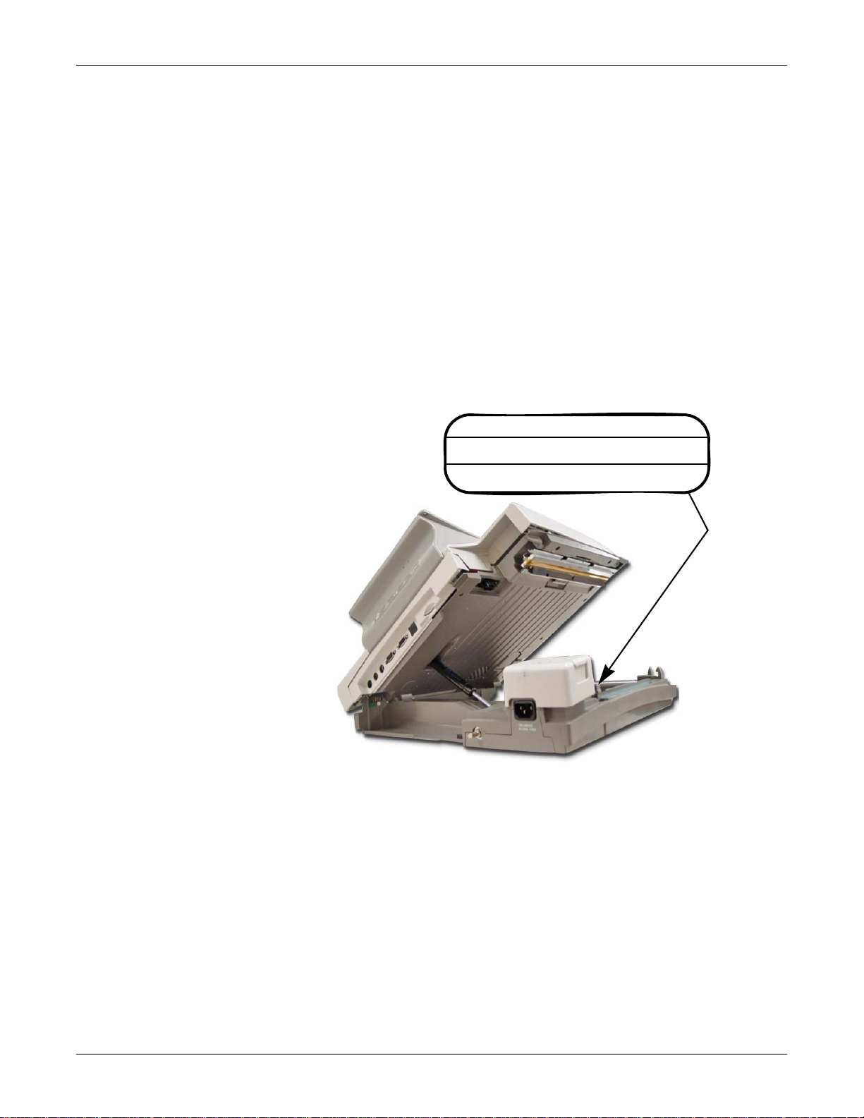
The serial number label is located inside the device as shown in the
following illustration.
Introduction: Service Information
SERIAL NUMBER
SERIAL NUMBER
LABEL
LABEL
Every GE Healthcare device has a unique serial number for
identification. The serial number is formatted as shown in
Number Format” on page 1-9.
NOTE
The examples shown are representative only. Your product label
may
differ.
“Serial
9A
1-8 MAC™ 3500 resting ECG analysis system Revision D
2021337-036
Page 19
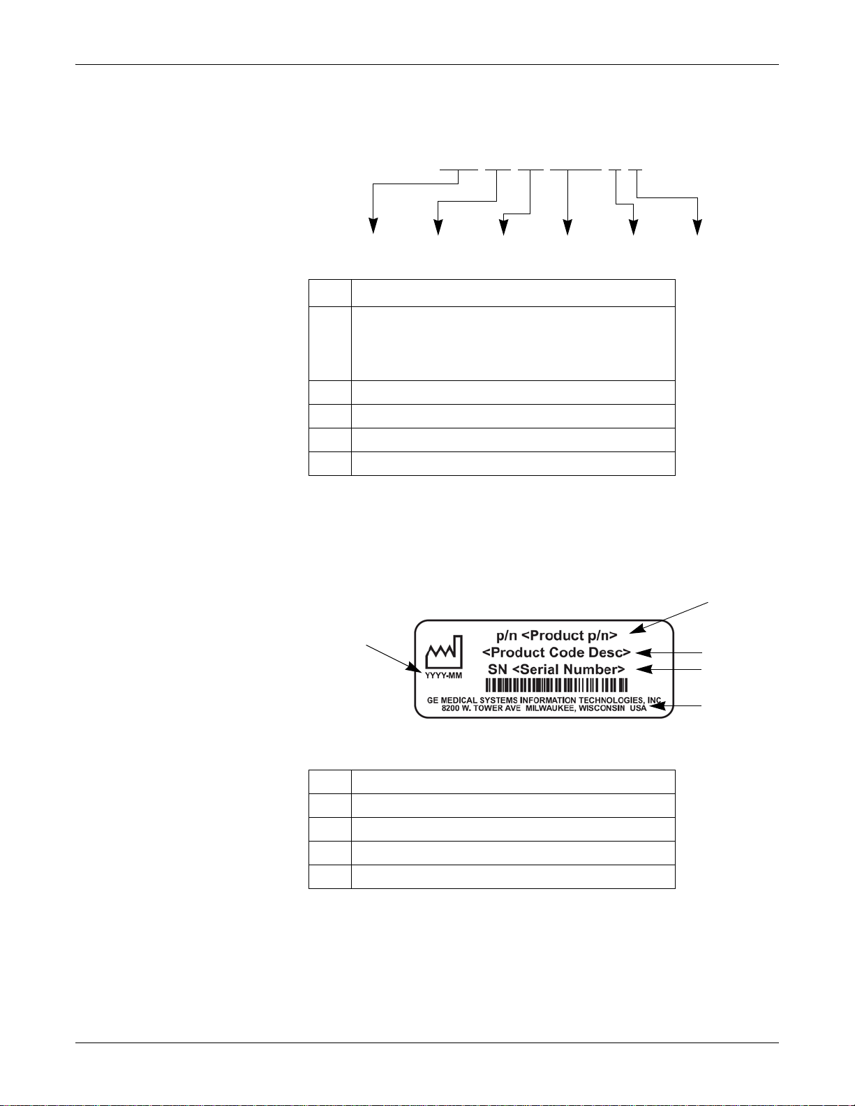
Serial Number Format
Introduction: Service Information
### ## ## #### # #
ABCDEF
Table 2. Serial Number Format
1
A
Product code
B Year manufactured (00-99)
06 = 2006
07 = 2007
(and so on)
C Fiscal week manufactured
D Production sequence number
E Manufacturing site
F Miscellaneous characteristic
Label Format
1. The product code for the MAC 3500 described in th is
manual is SCA.
B
A
C
D
E
Table 3. Equipment Identification Label
A Date of manufacture in YYYY-MM format
B Part number of product
C Product code description
D Serial number (described above)
E Manufacturing site
Revision D MAC™ 3500 resting ECG analysis system 1-9
2021337-036
Page 20

Introduction: Service Information
1-10 MAC™ 3500 resting ECG analysis system Revision D
2021337-036
Page 21

2 Equipment Overview
Revision D MAC™ 3500 resting ECG analysis system 2-1
2021337-036
Page 22

For your notes
2-2 MAC™ 3500 resting ECG analysis system Revision D
2021337-036
Page 23
Equipment Overview: General Description
General Description
The MAC™ 3500 resting ECG analysis system is a 12-lead, 12-channel
system with a 6.5 inch (165 mm) diagonal display, active patient cable,
and battery operation. There are also options for communication
capabilities.
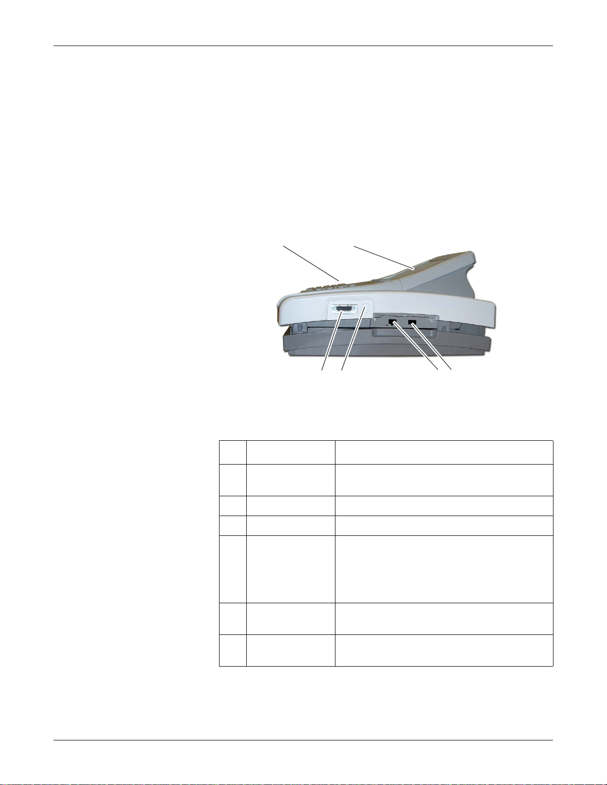
Side View
A
F
Name Description
A keyboard Press the keyboard keys to control the system or to enter
B display screen View the waveform and text data.
C modem port Connect the telephone cable here (optional feature)
E
data.
B
CD
104A
D LAN port Connect to the LAN here (optional feature)
The green LED on the right side of this port indicates
a
good ethernet link.
The amber LED on the left side of this port flashes to
indicate network traffic.
E KISS pump
connector
F ECG signal input
connector
Revision D MAC™ 3500 resting ECG analysis system 2-3
2021337-036
Connect the KISS pump here (optional feature).
Connect the patient cable here.
Page 24

Back View
Equipment Overview: General Description
105A
A BCD
Name Description
A back panel connectors Connect peripheral devices here.
B Secure Digital card slot Insert Secure Digital card for external storage here.
C ground lug Connect non-grounded peripheral devices to ensure
equipotential.
D main AC power Insert the main AC power cable.
2-4 MAC™ 3500 resting ECG analysis system Revision D
2021337-036
Page 25
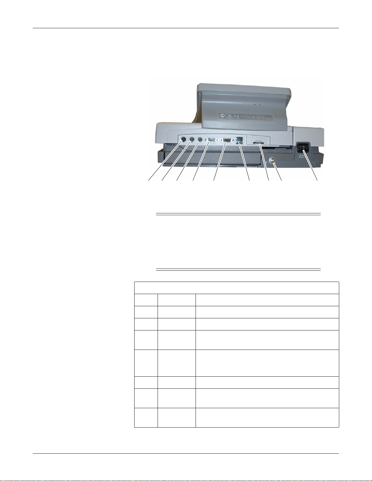
Equipment Overview: Connector Identification
Connector Identification
A BC D E F GH I
WARNING
LEAKAGE CURRENT – Keep leakage current within
acceptable limits when connecting auxiliary equipment
to this device.
Total system leakage must not exceed 300 microamperes
(United States) or 500 microamperes (international).
Table 4. Back Panel Connectors
Item Name Description
A A Connect an optional card reader or optional bar code reader
B 1 External GE KISS pump connection.
C 2 Connect a local transmission cable, serial line, modem, or client
bridge (wireless option).
D ANA/TTL Connect a device requiring analog data or TTL trigger
(ultrasound, stress echo, ergometer, analog treadmill, blood
pressure units, etc.).
106A
E EXT.VID. Connect an external video display.
F IR Point at a MAC 5000, MAC 5500, MAC 3500, or MUSE
system’s IR transceiver to transmit or receive ECG data.
G card slot Insert the system card into this slot to archive or restore data
from external media or to update software.
Revision D MAC™ 3500 resting ECG analysis system 2-5
2021337-036
Page 26

Equipment Overview: Connector Identification
Table 4. Back Panel Connectors (Continued)
H ground lug Connect non-grounded peripheral devices to ensure
equipotential.
I main AC power Insert the main AC power cable.
2-6 MAC™ 3500 resting ECG analysis system Revision D
2021337-036
Page 27
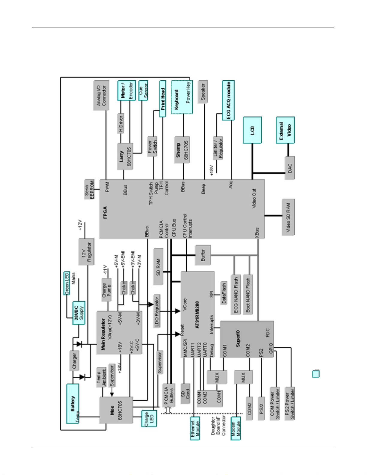
Equipment Overview: Detailed Description
Detailed Description
Block Diagram
MAC 3500 Basic Block Diagram
Not part of motherboard
79A
Revision D MAC™ 3500 resting ECG analysis system 2-7
2021337-036
Page 28

Equipment Overview: Theory of Operation
Theory of Operation
Overview / Block Diagram
The MAC 3500 CPU board contains all of the circuitry for the MAC™
3500 resting ECG analysis system except for the line power supply,
acquisition module, keyboard and display. Although the MAC 3500 runs
software derived from products based on the Max-1 architecture
(running on the C-Exec operating system), it has almost nothing in
common with that hardware family. Components listed in this section
refer to the 801212-007 CPU board assembly.
The CPU board contains the following:
64 MB SDRAM (holds both code and data)
32 MB SDRAM acts as video frame memory
32 MB NAND Flash (holds FPGA configuration and system code)
32 MB NAND Flash for ECG Record storage
128 KB Boot Data Flash (holds primary boot image)
CRT video DACs
External 12 Volt Power Switch
Acquisition Module Transceiver / Power Switch
Printhead Power Switches and Pixel Test Circuit
Daughter Board Interface which support LAN and modem
Switch Mode Power Supplies
3.3 Volt for Logic, LCD
5 Volt for Logic, Printer,
12 Volt for LCD backlight, External Com Port Power
Battery Charger
-12 Charge Pump for Analog Circuits
Linear Power Supplies
1.8 Volt (AT91RM9200 Core and FPGA Core)
2.5 Volt Reference
3.3 Volt for System Supervisor (Moe Stooge)
12 Volt for Analog Circuits
Crystals / Clocks
24 MHz Oscillator for FPGA
32.768 Khz Real Time Clock for Super IO chip.
32.768 Khz (AT91RM9200)
18.432 Mhz (AT91RM9200)
4 Mhz (3 devices, 1 for each Stooge)
2-8 MAC™ 3500 resting ECG analysis system Revision D
2021337-036
Page 29

Equipment Overview: Theory of Operation
Atmel AT91RM9200 CPU Containing:
Incorporates the ARM920T™ ARM® Thumb™ Processor
- 200 MIPS at 180 MHz, Memory Management Unit
- 16-KByte Data Cache, 16-KByte Instruction Cache,
Write
Buffer
- In-circuit Emulator including Debug Communication
Channel
- Mid-level Implementation Embedded Trace Macrocell
(256-ball BGA Package Only)
Low Power: 30.4 mA on VDDCORE, 3.1 mA in Standby Mode
Additional Embedded Memories
- 16K Bytes of SRAM and 128K Bytes of ROM
External Bus Interface (EBI)
- Supports SDRAM, Static Memory, Burst Flash, Glueless
Connection to CompactFlash®, SmartMedia
NAND
System Peripherals for Enhanced Performance:
Flash
™ and
- Enhanced Clock Generator and Power Management
Controller
- Two On-chip Oscillators with Two PLLs
- Very Slow Clock Operating Mode and Software Power
Optimization Capabilities
- Four Programmable External Clock Signals
- System Timer Including Periodic Interrupt, Watchdog and
Second Counter
- Real-time Clock with Alarm Interrupt
- Debug Unit, Two-wire UART and Support for Debug
Communication Channel
- Advanced Interrupt Controller with 8-level Priority,
Individually Maskable Vectored Interrupt Sources, Spurious
Interrupt Protected
- Seven External Interrupt Sources and One Fast Interrupt
Source
- Four 32-bit PIO Controllers with Up to 122 Programmable
I/O Lines, Input Change Interrupt and Open-drain
Capability on Each Line
- 20-channel Peripheral Data Controller (DMA)
Multimedia Card Interface (MCI)
- Automatic Protocol Control and Fast Automatic Data
Transfers
- MMC and SD Memory Card-compliant, Supports Up to Two
SD Memory Cards
Three Synchronous Serial Controllers (SSC)
- Independent Clock and Frame Sync Signals for Each
Receiver and Transmitter
- I 2 S Analog Interface Support, Time Division Multiplex
Support
- High-speed Continuous Data Stream Capabilities with 32-bit
Data Transfer
Revision D MAC™ 3500 resting ECG analysis system 2-9
2021337-036
Page 30

Equipment Overview: Theory of Operation
Four Universal Synchronous/Asynchronous Receiver/
Transmitters (USART)
- Support for ISO7816 T0/T1 Smart Card
- Hardware and Software Handshaking
- RS485 Support, IrDA Up To 115 Kbps
- Full Modem Control Lines on USART1
Master/Slave Serial Peripheral Interface (SPI)
- 8- to 16-bit Programmable Data Length, 4 External
Peripheral Chip Selects
Two 3-channel, 16-bit Timer/Counters (TC)
- Three External Clock Inputs, Two Multi-purpose I/O Pins per
Channel
- Double PWM Generation, Capture/Waveform Mode, Up/
Down Capability
FPGA Containing:
XBus Controller
LCD Controller with SDRAM Frame Buffer.
Video Waveform Scroller
Interrupt Controller
System Interrupt Generator
Acquisition Module Interface
Thermal Printhead Interface
Serial EEPROM Interface
BBus Controller
Four PWM Analog Outputs
Beep Generator
PC Card Interface
A PC Super I/O controller containing:
Two Serial Ports (one dual mode RS-232 / IrDA)
Clock/Calendar (Y2K compliant)
PS-2 Keyboard Port (for card and barcode readers)
Floppy Disk Controller
Three Peripheral Microcontrollers (The Three Stooges):
System Supervisor / Battery Charger-Gauge (Moe)
Printer Motor Controller / Analog Input (Larry)
Keyboard Interface (Shemp)
2-10 MAC™ 3500 resting ECG analysis system Revision D
2021337-036
Page 31

Power Supplies
+3V-C
Equipment Overview: Theory of Operation
The MAC™ 3500 resting ECG analysis system requires several regulated
voltages for operation of its various components. The Main Regulator
provides most of the supply rails. The supply rails are:
MAC™ 3500 resting ECG analysis system is never truly “off.” The system
supervisor microcontroller (MOE) must constantly monitor the power
key and perform battery charging/gauging. The clock/calendar in the
Super I/O chip must also maintain time/date when the machine is off.
These functions are powered from the +3V-C rail, which provides power
continuously from the battery pack regardless of the state of the rest of
the system. The Main Regulator produces +3V-C directly from the
battery rail via an internal low current linear regulator. Only 5mA are
available from +3V-C, so it must be used sparingly.
NOTE
The MAX782’s low current regulator is dreadfully inefficient.
Regulator Q current appears to be about 3x the load current. This
makes conservation of load on +3V-C crucial.
+3V-M
+3V-EMI
+5V-M
+5V-EMI
Most of the MAC 3500 hardware runs from +3V-M. The MAX782
provides this rail from the battery via a PWM synchronous switching
regulator. Moe controls +3V-M in tandem with +5V-M.
This is simply an RF blocked feed from +3V-M. +3V-M load is contained
within the CPU board. Power for devices for external functions is
supplied by +3V-EMI. The isolation of +3V-EMI from +3V-M may be
unnecessary as the concept has never been tested for its effect.
The MAC™ 3500 resting ECG analysis system is not fully in the 3V age.
The Super I/O and thermal printhead require 5V power. The MAX782
provides this rail via another PWM synchronous switching regulator.
Moe controls +5V-M in tandem with +3V-M.
Similar to +3V-EMI, this rail is an RF blocked feed from +5V-M, used to
power devices for external functions. The isolation of +5V-EMI from
+5V-M may be unnecessary as the concept has never been tested for its
effect.
Revision D MAC™ 3500 resting ECG analysis system 2-11
2021337-036
Page 32

+18V
+1.8V
+12V
Equipment Overview: Theory of Operation
The Main Regulator’s 5V switching output also supports generation of a
non-regulated 18V rail, which is used to provide power for the acquisition
module. By providing the acquisition module with 11.5V linearly
regulated power from the +18V rail of the main regulator rather than the
main 12V regulator (U17), acquisition is not affected by excessive current
draw from the printer motor or external loads on the COM ports
(especially the KISS pump). The acquisition module's power
requirements are modest, so efficiency is not a pressing concern and the
lower efficiency of this approach is acceptable.
The Atmel CPU and FPGA (Xilinx Spartan 2) operates their internal
core logic at 1.8V, while their I/O ring runs at the system standard 3.3V.
The 1.8 Volt regulator, a low dropout linear regulator, drops +3V-M to
1.8V for use as a core supply.
REF2V5
The paper motor drive circuit, LCD backlight and external COM ports all
require 12V. The Main Regulator’s 18V output cannot provide sufficient
current for all of the systems 12V loads, so a secondary 12V regulator is
required. The Main 12V Regulator (U17), a switching buck regulator,
provides the higher currents needed by these loads. A P-channel
MOSFET (Q1) switch precedes the regulator to provide on/off control.
Gate capacitor C12 slows the turn on/off time of the MOSFET switch to
eliminate switching transients. The voltage divider created by R133,134
prevents the full supply rail from being impressed across Q1’s gate when
on. This protection is necessary, as the maximum Vgs of the MOSFET is
less than the peak supply voltage.
The high power rails are neither precise nor quiet enough to be used as
the reference for analog input/output or internal measurement circuits.
The Analog Reference Regulator (U50), a 2.5V shunt regulator, provides
a quiet and stable reference voltage for such purposes. VREF is derived
from +5V-EMI rather than +3V-EMI to minimize the change in reference
current with changes in input rail voltage. The difference between 5V
and 2.5V is three times greater than the difference between 3.3V and
2.5V. If the absolute ripple on both supplies is the same, the modulation
of reference current will be 3 times less if power is derived from +5V.
2-12 MAC™ 3500 resting ECG analysis system Revision D
2021337-036
Page 33

VAna+, VAna-
Clocks
Super I/O and FPGA
Equipment Overview: Theory of Operation
The analog output circuitry is powered by a low current switched 12V
rail, provided by the Main Regulator. VAna+ provides the positive supply
for the output op-amps. A charge pump voltage inverter is provided to
produce an approximate -11V rail for the op-amps. Although only the
ECG output is bipolar, all output amplifiers are driven from VAna-.
A
short circuit on either of the unipolar DC outputs could load VAnasufficiently to affect the negative peak swing of the ECG output. The
ECG and DC outputs are not required to operate correctly in the
presence of abnormal loads.
Both of these devices use the 24 Mhz clock oscillator Y5 to drive their
internal requirements for various clock frequencies. The main function of
the Super I/O IC is for serial port communication and real time clock; all
the needed timing comes from this oscillator. The FPGA provides many
functions including the acquisition interface, the printer interface, and
the Stooges interface (Bbus) to name a few. The FPGA uses a built-in
frequency doubler to raise this 24 Mhz clock to 48 Mhz for internal use.
All functions inside the FPGA use the clocks derived from 48MHz. The
main derived clocks are:
1 MHz for acquisition interface
4 MHz for printer data shift clock interface.
4 MHz for EEPROM data shift clock
24MHz for VGA LCD panel clock.
The VGA LCD controller, that include the SDRAM frame buffer
controller use 59.904 MHz external memory clock from ATMEL CPU in
addition to the 48MHz FPGA clock
CPU ATMEL AT91RM9200
The ATMEL AT91RM9200 has two oscillators. Slow Clock oscillator and
Main Oscillator. The Slow Clock Oscillator uses 32,768 KHz crystal for
clock generation. The CPU runs in Slow Clock mode (@48MHz) after
system reset. Slow Clock is also used by the built-in RTC. But the -006
and -007 boards do not use the ATMEL RTC for the system timing
requirements. The Main oscillator uses 18.432 MHz crystal. Processor
clock (179.712 MHz), Master clock (59.904) for external Bus Interface
and Peripheral Clocks are derived from the main oscillator by the Master
Clock Controller.
Revision D MAC™ 3500 resting ECG analysis system 2-13
2021337-036
Page 34

CPU (Stooges)
RTC
CPU
Equipment Overview: Theory of Operation
Each of the three Stooges has its own 4 Mhz ceramic resonator for use in
generating their respective clocks.
The Real Time Clock of the system is provided as a part of the Super I/O
controller. The timing for this function is derived from its own 32.768
Khz crystal.
The ATMEL AT91RM9200 replaces the Strong ARM SA1110 used in
-005 board. The AT91RM9200 uses high performance, low power
consumption and high code density ARM920T processor core. One of the
major difference between SA1110 and AT91RM9200 is the absence of
built in LCD controller and 16-bit static memory controller. StrongARM
support 32 bit memory interface. The Processor Clock and External Bus
speed is limited to 180 and 80 MHz when compare with the 206 and 103
MHz of StrongARM. But having an external LCD controller with a
separate video memory interface compensates overall performance of the
-006 board.
External Bus Interface
The external bus interface width is limited to 16bit in ATMEL CPU
when compare with the 32 bit interface of StrongARM. All the non VGA
FPGA registers are either 8 bit or 16 bit wide. However all these were
accessed using 32 bit access in -005 board and aligned to 32 bit word. To
port the applications that was written for the 32 bit access, all the Non
VGA memory space within the FPGA are accessed in 32 bit mode in -006
board. When the ATMEL static memory controller see a 32 bit memory
access, it perform two consecutive 16 bit access. To avoid over writing of
FPGA register with upper 16-Byte data, The FPGA register access logic
is designed in such a way that, the FPGA ignores upper 16 byte access.
However for access to the pixel data FIFO, the upper 16 bit contains
valid data and the this will be loaded into the next 16 bit word.
The VGA registers are accessed using 32 bit access. The Frame Buffer
area can be accessed either in 32 bit word mode or byte mode.
2-14 MAC™ 3500 resting ECG analysis system Revision D
2021337-036
Page 35

Boot Loader
Equipment Overview: Theory of Operation
In the -005 board, after power ON, the FPGA gets configured using the
micro controller Curly. The FPGA emulate the boot ROM and the start
up code was placed in the Boot ROM from the smart media card by the
micro controller Curly.
The ATMEL AT91RM9200 has built in boot program in the internal
ROM. The -006 and -007 boards utilize the ATMEL CPU itself for
bringing up the board. Since the service of Curly is no longer required, it
is removed from the board. At power ON if the BMS pin is high, ATMEL
starts executing boot code in the internal ROM. The boot program looks
for valid code in SPI data flash (U66) and if found, downloads the
program into SRAM and starts executing from SRAM after remap. The
-006 and -007 boot program loads primary boot code into the SDRAM
after initializing it. The primary boot program reads the PCB ID code
from three port pins and then searches the NAND Flash for a matching
FPGA configuration image (pages with ID “Xn” where n is the 3-bit PCB
ID code 1-8 plus one). Once located, the configuration image is loaded
into the FPGA in fly by fashion. Blinking of LED DS3 at 1 Hz indicates
successful completion of FPGA configuration. The primary boot program
then loads the secondary boot code from NAND to SDRAM and transfers
the control to the secondary boot program. Buffer U55 is used to get the
direct CPU access to NAND Flash. To configure the FPGA in fly-by
mode, the data needs to be present at the Xbus while toggling CCLK.
This is achieved by toggling the NAND_RE* alternately with CCLK. The
NAND_RE* needs to be under the GPIO control instead of static memory
controller to do this. The ALE and CLE are also controlled in GPIO mode
and tied to low level during read cycle while configuring the FPGA. The
CLE and ALE acts as address line A23 and A25, respectively, during
Address and command cycle as well as access other than FPGA
configuration. The reason for omitting A24 is because of AT91RM9200
silicon bug. The A24 does not work like an address pin. It can work only
as GPIO line.
The primary boot code also contains the application for software update.
If there is no valid code in the NAND FLASH, the primary boot code
looks for SD Card and if detected it down load the code from the SD Card
to NAND Flash and reset the system. If the primary boot code can not
detect a valid code within 2 minutes 6 seconds, ‘Moe’ shuts down the
system. The status of software update is indicated on DS1 and DS2. The
DS1 and DS2 are not visible once the top cover is in place. The ‘Moe’
flashes amber charge LED at 1Hz to indicate that software update is in
progress. But it can not provide the completion status. Refer the table
below for the status messages from LEDs DS1 and DS2 during primary
boot software update.
DS1 Red DS2 (Green) Status
Off Flashing No SD card detected for software updated
Off‘ On Copying image files from SD card to SDRAM
Revision D MAC™ 3500 resting ECG analysis system 2-15
2021337-036
Page 36

Equipment Overview: Theory of Operation
DS1 Red DS2 (Green) Status
Off Off Erasing and / or formatting the NAND Flash.
Applicable only during the software update
process.
On Off Programming the NAND Flash
Flashing Flashing Successful completion of programming
Flashing Off Error - Could program all the image files. But
error in programming the status page 'Z0'.
On On Error - Could not program all the image files
as well as the status page 'Z0'.
On Flashing Error - Could not program all the image files.
But the status page 'Z0' updated successfully
A copy of primary boot program (pages with ID “Bn” where n is the 3-bit
PCB ID code 1-8) is kept in NAND flash. This is updated whenever
software update happens. For -006 and -007 boards, the FPGA image
and Primary boot code image IDs are X3 and B3 respectively.
FPGA Internal Logic
The primary boot program can do a forceful software update, even if a
valid program is present in the NAND Flash, by using a special SD Card,
which has a file, update.com, in the root directory. The service menu
provides a provision to update the SPI data flash with the primary boot
program copy residing the NAND Flash.
All of the MAC™ 3500 resting ECG analysis system’s proprietary
hardware is contained in a single Xilinx FPGA that contains:
XBus Controller
Video Interface
LCD Controller with SDRAM frame buffer
Video Waveform Scroller
Interrupt Controller
System Interrupt Generator
Acquisition Module Interface
Thermal Printhead Interface
Serial EEPROM Interface
BBus Interface
Four PWM Analog Outputs
Beep Generator
2-16 MAC™ 3500 resting ECG analysis system Revision D
2021337-036
Page 37

Board ID Register
Equipment Overview: Theory of Operation
The following descriptions give an overview of the FPGA’s functionality.
For detailed information on the internal circuitry, refer to the schematic.
For a programmer’s eye view of the FPGA, see the source file
“hardware.h”. Where appropriate, circuitry external to the FPGA is
also
described.
It is necessary to identify versions/revisions of the CPU board
automatically in the field. The ATMEL primary boot code read the boot
ID port pins to identify the FPGA image and startup code required for
the board. The board ID register contains a hardwired three bit code
that tracks the FPGA image number, indicating to the ATMEL just
which FPGA image has been loaded. Three additional FPGA inputs are
reflected in this register to allow further refinement of the board
identity. Resistors (R98 and R99 through R129) are used to program the
board ID.
Board ID Code Versions of the 801212 CPU Board assembly
000h -001, -002
XBus Controller
Video Interface
001h -003
002h -004 (not used)
003h -005
004h not used
005h -006
006h -007
To reduce loading on the high speed processor address and data busses,
a
slow speed byte bus is provided for peripheral interface. The Super I/O
controller and NAND Flash ICs are both located on this bus. Unlike the
3.3V only main data/address busses, XBus is compatible with both 5V
and 3.3V logic. To maintain software compatibility with previous board
versions, the low order address byte is not used by XBus. Starting XBus
addressing with A8 also produces Super I/O addresses that easily map to
their standard PC equivalents (simply append 0x00 to a datasheet Super
I/O address offset to get a MAC 3500 Super I/O address offset).
LCD Controller with SDRAM Frame Buffer
Continuing problems with LCD controller part obsolescence have made
implementation of a controller design in the FPGA attractive. The MAC
3500 GUI software does not depend on sophisticated video functionality,
so an FPGA implementation of a suitable display controller can be
reasonably compact. By implementing the controller in the FPGA (using
Revision D MAC™ 3500 resting ECG analysis system 2-17
2021337-036
Page 38

Equipment Overview: Theory of Operation
the VHDL hardware description language) obsolescence is avoided, and
future upgrades are easily implemented.
The LCD controller is comprised of these functional blocks:
Video Timing Generator (See “Video Timing” on page 2-18)
SDRAM Frame Buffer Controller (See “SDRAM Frame Buffer
Controller” on page 2-18)
Format pack/unpack logic (See “Format pack/unpack logic” on
page 2-19)
Line buffer (See “Line Buffer” on page 2-20)
Fill Engine (See “Fill Engine” on page 2-20)
Main State Machine (See “Main State Machine” on page 2-21)
Interrupt management (See “Interrupt Management” on page 2-22)
Video Timing – The LCD controller generates video pixel and line
timing from a 60Mhz clock inside the FPGA. The timing generator
consists of one counter for timing pixels within a line (including
generation of horizontal sync, horizontal front and back porches, and
LCD data enable timing) and another for timing lines with a frame
(including generation of vertical sync, vertical front and back porches
and generation of Line FIFO fill requests). In addition, the timing
generator increments a memory address register by the line pitch (640)
at the beginning of each video line, so the Line FIFO knows where to get
the next line of pixels. The controller produces fixed timing for a 640x480
LCD, and requires no initialization to produce that timing. Support for
future, higher resolution displays, can be obtained by modifying the
source code for the controller itself, providing the most efficient hardware
implementation possible.
SDRAM Frame Buffer Controller – The LCD obtains pixel data from
a 1Mbyte region of a 32Mbyte, 16-bit wide synchronous DRAM
(SDRAM). The SDRAM buffer is shared by the display controller and the
CPU, allowing system software to directly manipulate screen pixels.
At power-up, SDRAMs must be configured for proper operation.
Properties such as RAS/CAS latency and burst length are written into a
control register in the SDRAM, and an initial burst of refresh cycles are
performed to prepare the memory array for operations. The SDRAM
controller does this all automatically at startup, requiring no
initialization by the CPU.
SDRAMs, being dynamic, require periodic refresh to maintain the
contents of the memory array. The SDRAM controller performs this
refresh automatically between accesses. All details of SDRAM bank
management and page boundary crossing are managed automatically in
the SDRAM controller. In addition, through the use of pipelining, the
SDRAM controller allows burst accesses to and from SDRAM at full
memory speed. All details of burst cycle management, including setup
and page boundary crossings, are handled transparently by the SDRAM
controller. The SDRAM memory clock is derived from the CPU memory
clock, and is passed out of the FPGA and back in to allow one of the
FPGA’s on-board DLLs to “zero out” all internal FPGA delays. This delay
compensation allows the SDRAM controller to operate reliably at very
high speeds (>= 100Mhz).
2-18 MAC™ 3500 resting ECG analysis system Revision D
2021337-036
Page 39

Equipment Overview: Theory of Operation
Format pack/unpack logic – The MAC 3500 display architecture is
based on the division of pixels into static and dynamic planes. As
discussed elsewhere, this technique allows the smooth scrolling of ECG
waveforms across the screen while buttons, annotations and other
graphics remain stationary. Previous generations of MAC 5000 display
controllers packed the five bits of each static plane pixels into the same
byte of memory as the three bits from the corresponding dynamic plane
pixel. In that scheme, pixel manipulations required the CPU to read the
combined pixel, modify either the static or dynamic component, and
write the result back to memory. Such read-modify-write operations are
time consuming.
In contrast, the FPGA implementation of the frame buffer takes
advantage of SDRAMs high speed, large size, individual byte
addressability, and 16-bit width, to access both the static (5 bits) and
dynamic (3 bits) portions of a pixel separately, and simultaneously.
The
SDRAM bus is effectively split into a “dynamic byte lane” and a
“static byte lane”. The resulting improvement in drawing algorithm
speed is substantial.
The 16-bit wide bus of the SDRAM allows each read/write cycle to access
two bytes of data. During writes, upper and lower byte strobes allow
independent writing of either or both bytes. During reads, both bytes are
always presented. Unneeded read data bits are ignored by the CPU. The
LCD controller takes advantage of the individual accessibility of the
bytes to eliminate the need for the CPU to pack and unpack the static
and dynamic pixels. At the expense of unused memory bits (a small
expense as less than 1/16th of the entire SDRAM space is needed at all)
the LCD controller maps the 5 bits of each static pixel into one SDRAM
byte lane (the static lane), and the 3 bits of each static pixel into the
other (the dynamic lane). Unused bits in each lane are written as zeroes,
and ignored on reading.
On the CPU side, the SDRAM frame buffer appears as two regions, the
static and dynamic planes. Each plane is a contiguous array of 480 lines
of 640 pixels each. Within the static plane, the lower 3 bits (the dynamic
bits) of each pixel byte are ignored on writes, and read as zeroes. Within
the dynamic plane, the upper 5 bits of each pixel byte (the static bits)
are
ignored on writes and read as zeroes. The dynamic plane is located
1/2 Mbyte above the static plane and address bit A19 is used to
differentiate between them. The interface from the LCD controller to the
CPU is 16-bits wide, allowing two pixel bytes to be moved in each read/
write cycle.
In the 16-bit wide SDRAM, each word (independently byte addressable)
contains both a static and a dynamic pixel byte, each in their own lanes.
When the CPU writes a pixel to the static plane, the upper five bits of the
byte are routed to the static byte lane (the lower three bits are set to
zero) and the dynamic byte lane is disabled. When the CPU reads a static
pixel, both the static and dynamic byte lanes are accessed, but only the
upper five bits of the static byte lane are passed on to the CPU (the lower
three bits are zeroed). Access to the dynamic plane proceed in much the
same manner, with the appropriate bits being routed to the dynamic byte
lane while the static byte lane is disabled.
Revision D MAC™ 3500 resting ECG analysis system 2-19
2021337-036
Page 40

Equipment Overview: Theory of Operation
Because each 16-bit word of SDRAM contains one pixel, and each 16-bit
access of the CPU into the frame buffer contains two, the LCD controller
must pack/unpack pixels on the fly. During writes, if the CPU signals a
single byte write, the LCD controller writes the byte onto the proper lane
(as determined by A19) of one memory word. If the CPU signals a two
byte write, the LCD controller queues a two cycle burst write into two
consecutive words of SDRAM. On reads, the LCD controller always reads
two pixels from memory and packs them into a single word for access by
the CPU, which may use both pixels, or ignore one.
By design, SDRAMs are faster when data can be moved in sequential
bursts. The Atmel ARM CPU asynchronous bus interface does not
support burst accesses, so the opportunity to burst is limited. The LCD
controller does take advantage of the 16-bit wide nature of the
asynchronous bus to allow bursts of two pixels into and out of memory
when possible. This nearly doubles frame buffer bandwidth over a
byte-at-a-time interface. Finally, as mentioned previously, the CPU is
able to manipulate individual pixels in either plane without resorting to
read-modify-write access cycles. This provides another twofold
improvement in memory bandwidth.
Line Buffer – Within each line of LCD video data, bytes must move
from the frame buffer to the scroller/CLUT in an unbroken stream at
48Mhz. Although the frame buffer is capable of burst transfers of
60Mpixels/sec, it cannot be depended on to maintain that speed for more
than one SDRAM page (256 pixels). At page boundaries, the SDRAM
must initiate a new page access, and potentially satisfy refresh
requirements. Since video lines are longer (640 pixels) than SDRAM
pages, some mechanism is required to smooth the flow of pixels from the
frame buffer to the LCD.
This smoothing is provided by a 1024 byte dual port line buffer,
implemented in a pair of FPGA block RAMs. At the end of each active
LCD line, the video timing generator requests a new line of pixels from
the frame buffer. The memory arbiter services the request by bursting
640 pixels from the frame buffer to the line buffer, using the video
address supplied by the timing controller. The entire line of 640 pixels is
moved at maximum memory speed, taking a little over 11μs to complete
at 60Mhz. The pixels are then clocked out of the line buffer and
presented to the scroller/CLUT at a constant 24Mhz, taking about 30μs
per line. Double buffering is not required, as the burst fill rate far
exceeds the 24Mhz drain rate, and the fill begins during the generation
of horizontal sync, giving the controller plenty of head start on filling the
line buffer before the timing generator begins draining them out.
To keep the control logic simple, and minimize SDRAM access overhead,
each 640 pixel line is transferred from SDRAM in one transaction. This
does hold off the ARM CPU for up to 11μs at a time, but as the ARM CPU
does not access the frame buffer often, this is not thought to be an issue.
Fill Engine – The 3500 routinely draws rectangular regions on screen
for use in dialog boxes and buttons. When drawn by the CPU, frame
buffer bandwidth becomes an issue, as random accesses to the SDRAM
buffer are inefficient, and many of them are required to fill large regions
of the display. To reduce both CPU and frame buffer loading, the LCD
controller provides a simple fill engine which automates the filling of
2-20 MAC™ 3500 resting ECG analysis system Revision D
2021337-036
Page 41

Equipment Overview: Theory of Operation
rectangular regions of the frame buffer, and takes advantage of the burst
capabilities of the SDRAM.
The fill engine interface is simple, consisting of four boundary registers
to define the fill region, and one register to record the fill value, and
planes to be filled. The fill engine can fill any value into any rectangular
region of the display in either or both planes simultaneously. The
bounding values (top, bottom, left, right) define the rectangle to be filled
in screen coordinates, with 0,0 at the upper left, and 639,479 at the
bottom right. The fill value contains both the dynamic (5) and static (3)
pixel bits as well as two plane enable bits.
After loading the boundary control registers, the CPU initiates the fill by
writing the requested fill value and plane enable bits to the fill value
register. The fill is then queued for the next video frame and the fill
engine becomes “busy”.
Fills are implemented synchronous with frame refresh. At the
completion of each line buffer fill request from the video timing generator
the fill engine checks to see if a fill is underway. If so, the current video
line position (from the timing generator) is compared to the top and
bottom boundary registers. If the current line is between the top and
bottom, the fill engine adds the left boundary value to the current line
memory address (as provided by the timing generator) and proceeds to
write the fill value into memory until the address matches the right
boundary. Depending on the width of the filled rectangle, fill bursts can
take anywhere from 100ns to 11μs.
In this way, the fill engine follows the video timing generator down the
screen, replacing pixels in the frame buffer immediately after they are
sent to the LCD. This synchronous operation makes efficient use of the
existing address generation hardware and provides “flicker-free” fills,
regardless of region size. If fills were unsynchronized, they would often
cross two successive display frames and result in visible tearing or
flicker. As a result of this frame synchronous operation, fills always take
one frame time, regardless of their size, and complete coincident with the
end of the frame.
Main State Machine – The SDRAM frame buffer is constantly in
demand by the CPU, the video timing controller and the fill engine. The
CPU manipulates pixels in the frame buffer in real time to construct the
visible display while the video timing controller manages the constant
stream of pixels from the frame buffer into the line buffer, and on to the
scroller/CLUT. At the same time, any requested fills must access the
frame buffer to write the requested fill region. When all three contend for
access to the frame buffer simultaneously, memory bandwidth can
exceed 100Mbytes/sec.
The Main State Machine manages all these competing requests on a
priority basis, with display refresh taking top priority, followed by fills
and finally CPU accesses. The state machine runs at 60Mhz, processing
line buffer fill requests from the video timing generator, fill requests
from the fill engine and read/write requests from the CPU. The 5.3 pack/
unpack logic and fill engine logic are actually various states of the Main
State Machine.
Revision D MAC™ 3500 resting ECG analysis system 2-21
2021337-036
Page 42

Equipment Overview: Theory of Operation
Interrupt Management – The LCD controller produces two interrupts
to notify the CPU of the completion of important tasks. At the end of the
active region of each display frame, the controller can generate an
interrupt to tell the CPU it has uncontested access to the frame buffer for
a short period, and to synchronize display related processes in the CPU
(such as waveform drawing and scrolling control). A similar interrupt is
provided to signal the completion of fills. Both interrupts may be
disabled and/or acknowledged in the system control registers.
Video Waveform Scroller
There are numerous ways of achieving a scrolling waveform, none of
which is supported by standard LCD controllers. The MAC 3500 provides
scrolling through FPGA hardware placed between the LCD controller
output and the LCD panel input.
To produce the scrolling effect it is necessary to maintain two virtual
image planes, one atop the other. Static (stationary) objects are drawn in
the static plane, which appears nearest the viewer and may be either
opaque or transparent. Dynamic (scrolling) objects are drawn in the
dynamic plane, which appears behind the static plane and is always
opaque, though not necessarily visible. The appearance of motion is
achieved by continuously changing the start point for display of the
dynamic plane from one video frame to the next.
Since the LCD controller does not support multiple image planes, it is
necessary to pack two planes of image data into a single frame buffer. On
the software side (during drawing) this is done by bit masking operations
that allow separate manipulation of two virtual pixels in each byte of
frame buffer memory. Each 8-bit byte holds a pair of pixels, one from the
static plane and one from the dynamic plane.
On the hardware side, part of each frame buffer byte (the static plane) is
played directly into the LCD after suitable color mapping. The remainder
of the byte (the dynamic plane) is stored in a 1 line temporal buffer before
being displayed. The amount of delay applied to the line buffer before
merging it with the static image data determines its placement on the
screen. By gradually changing the delay, the dynamic image can be made
to scroll.
Color Lookup Table (CLUT)
Generally the dynamic plane is filled with waveforms and perhaps a few
characters of text. The static plane often contains text messages, icons,
buttons and graphics. The greater variety of object types displayed in the
static plane demands a wider range of colors. For this reason, each video
data byte is split asymmetrically into five bits of static pixel data and
three bits of dynamic pixel data. This has come to be known as 5.3
format.
The 5.3 format provides a palette of 2^3=8 colors for dynamic objects and
(2^5)-1=31 colors for static objects (1 of the colors is transparent, leaving
31 real colors). In practice, to “freeze” dynamic objects in the static plane
requires that the 8 dynamic colors be replicated in the static color map,
leaving only 31-8=23 new colors available for static objects. The FPGA
implements a writable color lookup table (CLUT) to map the pixel values
to sensible colors on the LCD. The CLUT provides 32- to 24-bit entries,
2-22 MAC™ 3500 resting ECG analysis system Revision D
2021337-036
Page 43

Equipment Overview: Theory of Operation
providing access to the complete color space offered by the LCD panel.
The color mapped LCD data is also fed to three external discrete 6-bit
DACs to create analog video for an external CRT.
Blank/Sync
External VGA monitors are supported with two styles of video sync
signal as well as retrace blanking.
Video Sync – The horizontal and vertical sync pulses from the LCD
controller are combined to produce a composite sync signal that is added
to the video signal. The video sync signal may be disabled under software
control to accommodate monitors that do not accept sync on green. The
sync signal is applied to all three video guns to eliminate color shifting in
systems that do not perform blank level video clamping.
TTL Sync – For monitors that do not accept sync on green, TTL logic
level horizontal and vertical sync signals are provided. These may be
enabled/disabled to implement a rudimentary “sleep” operation on
Energy Star compliant monitors.
Blank – Unlike LC displays, CRT’s emit light from more than just their
active display surface. The electron beam is visible even during retrace
and precautions must be taken to ensure that the guns are off in nonactive areas of the display. To ensure black borders on external monitors
(and reset the DC restore clamps in the video output buffers). The CLUT
video passes through a gating register before leaving the FPGA. This
allows the LCD DE (display enable) signal to force the guns to a blanking
level during inactive portions of the display frame.
Interrupt Controller
ATMEL AT91RM9200 supports one external fast interrupt input(FIQ)
and seven external interrupt inputs. In addition all the GPIO lines can
act as an interrupt inputs. All the dedicated external interrupt inputs
are multiplexed with GPIO ports. The FPGA interrupt logic combines the
interrupts form System Timer, Acquisition interface, BBUS interface,
Thermal printhead interface and LCD controller to FIQ and Slow
Interrupt. The FIQ and Slow Interrupt from FPGA Interrupt controller
are fed to processor FIQ and IRQ0 respectively. For more detail on the
operation of the interrupt mask/status registers, see the source file
“hardware.h”.
Revision D MAC™ 3500 resting ECG analysis system 2-23
2021337-036
Page 44

System Interrupt Timer
A 1KHz timer generates system interrupts (which may be routed to FIQ
or IRQ) once every millisecond. This interrupt provides the foundation
for all operating system timers.
Acquisition Module Interface
Overview
The MAC 3500 acquisition module communication protocol is different
from previous generations in several key respects:
1. Acquisition module timing is synchronized to the system.
2. Data is framed and has checksum.
Equipment Overview: Theory of Operation
There is no longer a need to play synchronizing games to get the
system (especially the display and printer) operating at the same
sampling rate as the acquisition module.
Previous acquisition modules offered rudimentary error detection.
This has finally been done nearly right. Each ECG data packet
contains a checksum.
3. Commands do not interrupt the data stream.
Previous generation acquisition modules required a cessation of
sampling to transmit commands to the module. This cessation of
sampling had the undesirable effect of breaking the acquisition
stream for operations as simple as changing the line filter frequency
or enabling or disabling the pace pulse detector. With the MAC 3500
this restriction is removed.
4. Buttons are supported.
Button state is communicated to the system in each ECG data
packet. This allows limited operator interaction with the machine via
the acquisition module.
Details
A constant reference clock frequency of 1MHz must be provided to the
acquisition module for generation of its internal sampling clocks. To
eliminate the need for data lines, command information is encoded on
this reference clock by altering its duty cycle. The FPGA provides a
serializer for the command bytes and clock generator/modulator to
transmit both the clock and command bits from the serializer. The
reference clock duty cycle is nominally 50%. By altering the duty cycle,
the DC content of the clock is changed. The acquisition module detects
this change in DC level. The timing of these shifts in DC offset encode
command data bits. A zero is encoded as a single shift in duty cycle from
50% to 25% lasting 31.25μs, followed by a refractory period of 468.8μs.
A
one is encoded as a pair of 31.25μs periods of 25% duty cycle separated
by 93.75μs, followed by a 343.8μs refractory period. In either case the
transmission of a single bit takes 500μs. A higher level protocol organizes
commands as groups of 8 bits.
Data from the acquisition module is packed into 257 bit NRZ frames. The
receive line idle state is high. The first bit of each packet is a zero and
2-24 MAC™ 3500 resting ECG analysis system Revision D
2021337-036
Page 45

Equipment Overview: Theory of Operation
serves as the packet start bit. As with a UART, the start bit is discarded.
The following 256 bits are received into a 16-word x 16-bit buffer for use
by the ATMEL CPU. The receive logic then looks for an idle period
(analogous to a UART stop bit) of at least 125μs in length as an indicator
that the link is again idle. Special marker words are inserted into the
ECG data packet (words 5, 10 and 15) to guarantee there will never be a
run of more than 80 bits of one’s (or zeros for that matter), so there is no
possibility of satisfying the idle period requirement in the middle of a
data packet.
Because the acquisition module clock is supplied by the FPGA, receive
timing errors are limited to phase uncertainty. By searching for the
beginning of the start bit in a fashion similar to that used by a UART,
the phase uncertainty is eliminated and the remainder of the packet may
be received without further synchronization. In practice, the FPGA uses
every edge in the receive data stream to re-sync its bit sampling circuit.
It is possible for the ECG data to be all zeros or ones, so runs of as many
as 80 zeros or ones could occur before a marker word is encountered in
the data stream (which contains at least one “1” and one “0” to break any
runs in the data).
The acquisition module supports a special “code update” mode for rapid
reprogramming of its on-board code memory. To increase the update
speed, the acquisition module echoes each uploaded code byte with a
single reply word rather than the usual 16-word data packet. The FPGA
receive logic provides a special 1 word reception mode to accommodate
this.
Thermal Printhead Interface
The ATMEL CPU sends print data to the thermal print head through a
buffered serial interface. The FPGA implements the data buffer,
serializer, strobe/latch pulse generator and power switch gate drive
pump. Special interlocks are implemented to prevent stuck strobe
signals or printing when the battery voltage is critically low.
Each print line requires 1728 bits of data. To conserve FPGA resources,
each line is divided into three chunks of 512 bits each, with one leftover
chunk of 192 bits. The FPGA provides a single 32 word x 16 bit buffer
(512 bits) to hold the print line data. After writing a chunk of data to the
buffer, the ATMEL CPU enables serialization of the data by reading one
of two registers (to support the serialization of either a full 512 bit or
partial 192-bit buffer). When the entire print line has been loaded, the
ATMEL CPU cues a print strobe by writing the required strobe width
value to the strobe/latch pulse generator.
When the strobe register contains a non-zero value, the power switch
gate pump produces a differential clock signal to drive an external diode
voltage doubler (CR132-133, C262-C264, R291). The output of the
voltage doubler drives the gate of a power MOSFET (Q11) that provides
power to the print head. R289 provides gate bleed off to ensure that Q11
turns off when the pump stops. C279 filters the doubler output to DC.
A special test mode is provided to allow testing of the thermal print head.
In test mode, print head power is disabled and the strobe signal is driven
Revision D MAC™ 3500 resting ECG analysis system 2-25
2021337-036
Page 46

Serial EEPROM Interface
BBus Interface
Equipment Overview: Theory of Operation
continuously. This allows individual print dots to be driven with a small
test current via a current source (Q107, R322, Z100) enabled by a level
shifter (Q106, R321) driven from a ATMEL GPIO line. Half of the
resulting printhead voltage drop (divider R323/324) may be measured to
either determine the dot’s resistance or at least determine if the dot is
open.
A standard four-wire SPI interface is provided for connection to a serial
EEPROM memory (CFGMEM). The ATMEL exchanges a byte of data
with the EEPROM by writing a value to the interface register. Data is
clocked at 4MHz; quickly enough that no interrupt support is required.
The ATMEL CPU polls a ready bit to determine when the transfer is
complete.
There are several I/O functions poorly suited to direct control by the
ATEML CPU, whether for reasons of software complexity or power
consumption. These I/O functions are provided by three 68HC705
microcontrollers placed strategically around the board (Moe, Larry and
Shemp). Each of these three microcontrollers must communicate with
the ATMEL CPU. BBus is a simple 1-wire point-to-point interface
designed specifically for this purpose. The FPGA provides a single BBus
transceiver and a 3-way bidirectional multiplexer to attach the three
BBus microcontrollers. For more Bbus information see the
microcontroller firmware source files. From the programmer’s
standpoint, BBus operates like SPI, where each transaction exchanges a
single byte between the host and peripheral.
PWM Analog Outputs
Four PWM channels are provided for the generation of analog outputs.
Three of the outputs are available on the Analog I/O connector; the
fourth is available internally for future use (if any). One of the PWM
channels provides 12-bit resolution at 6KHz cycle rate; the other three
provide 8-bit resolution at 96KHz cycle rate. The ATMEL CPU simply
writes the desired value into a PWM data register and the output duty
cycle changes on the next PWM cycle. External analog circuitry converts
the PWM logic signals to smooth analog voltages. The 12-bit PWM
channel is intended for ECG output and produces a swing of +10 to -10V.
The two 8-bit channels provide a unipolar 10V output. Regardless of the
resolution or swing range of each PWM channel, the FPGA treats the
data value as a signed 16-bit number representing a voltage from +10V
(0x7fff) to -10V(0x8000). Logic in each PWM channel ensures that the
closest possible voltage is generated for each data value (ex. 0x8000 on
an 8-bit channel produces zero volts output).
The FPGA PWM output signals contain a substantial amount of noise
from +3V-M supply fluctuations. To reduce noise and establish an
accurate reference level, the PWM signals are buffered by CMOS
inverters (U20) that are powered from REF2V5. Although the CMOS
inverters are powered by 2.5 Volts but are driven by 3.3 Volt logic, no
2-26 MAC™ 3500 resting ECG analysis system Revision D
2021337-036
Page 47

Beep Generator
Equipment Overview: Theory of Operation
problem exists as this is allowed with VHC logic. The PWM output
signals are then low pass filtered (R186,C186, and so on) before being
passed to the output amplifiers. The ECG output channel amplifier
injects an offset current derived from REF2V5 to achieve bipolar
operation. The DC outputs operate in unipolar fashion, eliminating the
vexing MAX-1 offset problems. No zero calibration is required for the DC
outputs. Since the ECG output is an AC signal, no offset adjust is
required there either.
The output amplifiers provide additional low pass filtering (R178,C178,
etc.). ESD protection and additional PWM carrier filtering is provided by
0.1μF filter capacitors. To prevent amplifier oscillation, blocking
resistors are placed between the amplifier outputs and the filter
capacitors.
A simple tone generator with two volume levels provides system beeps
and key clicks. Frequencies of 250Hz, 500Hz and 1KHz are provided at
both low and high volume. The logic level output signal drives LS1
through an open collector transistor driver Q100. Full volume is achieved
by driving the fundamental beep tone directly to the speaker. Half
volume is achieved by gating the speaker signal with a 48KHz square
wave, reducing the amplitude by 50%. The LS1 is also used by the
communication board for modem sound. The modem speaker signal from
the module is amplified and driven though Q101.
PC Card Logic
SDRAM
NAND Flash
The -006 and -007 boards are designed to support multiple products and
one of the requirement during the design phase was the support for PC
Card, through a daughter board. But this requirement was removed later
on. The PC Card logic uses the two ATMEL chip select signals and bus
control signals to generate, IO, Memory and Attribute memory access to
PC Card. The PC Card bus controls signals from FPGA and the address
and data lines form ATMEL are buffered and terminated to daughter
board interface connector J21.
Program code and working data is stored in a four 4MWord bank of
32-bit wide memory (64Mbytes). This memory is made up of two 256
Mbit SDRAMs each 16 bits wide. All bus timing and refresh control is
performed by the ATMEL CPU SDRAM controller. The SDRAM clock
rate is one third of the ATMEL CPU clock or 59.904 Mhz. Though the
size requirement is less, the video frame buffer also use 256Mbit
SDRAM.
There are two 32 Mbytes NAND Flash in the -007 board. One is used for
storing FPGA configuration data and system software. The other is for
data storage. The access to NAND flash is through a dedicated smart
Revision D MAC™ 3500 resting ECG analysis system 2-27
2021337-036
Page 48

Equipment Overview: Theory of Operation
media interface logic provided by ATMEL CPU. NAND flash chips are
accessed through the buffer U55 instead of Xbus. The NAND Flash
control signals are changed to GPIO mode while configuring FPGA in fly
by fashion. Wear-leveling algorithm is implemented for the data storage
NAND flash to extend the life.
Secure Digital Card Interface
The SD card interface is provided to support software update and
external data storage application. The socket provide card detection and
write protect status signal. ATMEL CPU has built in secure digital card
interface controller. But there is a bug in the current revision of the
ATMEL CPU, which swaps bits within the transmitted / received
nibbles. Since the software overhead to correct this is high, SD card
interface support only SPI mode. However all the SD card interface
signals are terminated at the connector through a set of resistors, which
are not placed, so that we can go for the true SD card interface in future.
Serial EEPROM
System setup information, option enables and other machine specific
data is stored in 32 KByte serial EEPROM. The SPI interface to the
EEPROM is provided by the FPGA.
Daughter Board Interface
The interface is realized using a 100 pin high speed connector. This
interface provide two serial interfaces, PC Card interface signals, USB
host and various power supply tappings. The PC Card interface and USB
interface are no longer in the requirement list. All the PC Card signals
are buffered. The buffer will be active only when a valid PC card is
inserted in the daughter board. Out of the two serial interfaces, one
provides full hardware handshaking. This is derived from the Super IO
COM2. The COM2 can be routed to either COM2 external connector or to
the daughter board interface using a multiplexer controlled using
ATMEL CPU port pins. The second serial interface has limited hardware
control and derived from ATMEL CPU UART 1.
VGA LCD/CRT Interface
An internal backlit LCD is home for the MAC 3500’s graphical interface.
In addition, external VGA monitors are supported for stress applications.
Control for a standard VGA format (640 x 480 pixels) LC display is
provided by the FPGA. The board is designed to support MAC3500 LCD
display also. Though the interface to LCD is same, external CCFL backlit
inverter is different for both display. Two connectors are provided for
external CCFL backlight inverters as well as two digital controls for On/
Off and brightness. While the FPGA is capable of directly driving the
LCD, external hardware is required to generate the analog video levels
expected by external VGA monitors.
2-28 MAC™ 3500 resting ECG analysis system Revision D
2021337-036
Page 49

Equipment Overview: Theory of Operation
LCD Panel EMI Reduction Components
To reduce EMI, 47pF capacitors have been added to all LCD digital lines.
In addition, 49.9
lines.
CRT Video DAC / Sync / Buffers
A triple 6-bit video DAC supports external analog VGA monitors. Only
one DAC/Level Shifter/Buffer will be described, as they are all identical
in function. The video output is referenced to a filtered tap (FB107, C29)
off the +3V-M supply rail and then level shifted back to ground.
Each DAC is comprised of six binary weighted resistors and a seventh
blank/sync signal resistor. The FPGA LCD data outputs sink current
through the 75
resistors. The voltage across the 75
all drive currents. Minor non-linearity is introduced in the DAC transfer
function by the fact that the summing junction varies in voltage with
DAC current.
Ω load resistor in proportion to their respective DAC
Ω resistors have been added to the video clock and Sync
Ω load resistor represents the sum of
The 3.3V referred video is shifted back to ground by a blocking capacitor.
The shifted video signal is buffered (and further shifted) by emitter
followers. Transistors clamp the negative excursions of the bases of the
emitter followers to one diode drop above ground, so the most negative
level at the emitter of the emitter followers is ground. Nominal full-scale
swing is 1VP-P (blank to white).
Bias for the base of the clamp transistors is provided by a 1.4V bias
supply consisting of a stack of two diode connected transistors (Q8). This
2Vbe bias exactly cancels the 2Vbe shift produced by the level clamp and
output buffer. Since all transistors are of the same type their Vbe’s track
well enough to provide acceptable output offset.
Diode clamps to ground and +3V-EMI provide ESD protection for the
VGA video and sync signals. The +3V-EMI rail is isolated from ESD
transients by FB106.
Acquisition Module Transceiver / Power Switch
MAC 3500 acquires ECG data with a new generation CAM acquisition
module. The FPGA provides the interface logic. Clocks and commands
are transmitted to the acquisition module on a balanced RS485 line.
Data is received similarly. Power to the acquisition module is provided
by a software controlled linear regulator.
Transceiver
To reduce EMI and susceptibility to noise, the acquisition module link is
implemented using RS-485 differential signaling. An RS485 interface
device provides the single ended to differential conversion in both
directions. Ferrite beads, capacitors and resistors are used to reduce EMI
on both sides of the transceiver.
Revision D MAC™ 3500 resting ECG analysis system 2-29
2021337-036
Page 50

Equipment Overview: Theory of Operation
Acquisition Power Regulator / Switch
To reduce standby power consumption, acquisition module power is
switchable. To protect the acquisition module from temporary brownouts
on the main 12V supply, power is obtained from a parasitic winding on
the main 5V regulator. This voltage is not well regulated, so a linear
regulator (U18) is used to provide regulation. This regulator also
contains an enable input which is used to disable power to the
acquisition module when not in use. The regulator also has built-in
current limit and over temperature shutdown for protection.
COMM Port Power Switch / Current Limiter / KISS Power
Power for external peripherals such as a modem is available on the
COMM connectors. Power may be turned on/off under software control
and current limiting is employed to protect internal operations from
excessive external loads. The current requirements and startup
conditions of the KISS pump require very high currents. U.L. limits
power to external devices to 15 Watts for reducing the likelihood of fire
during overload. The KISS and U.L. requirements conflict to a degree
that a simple current limiter will not satisfy both needs therefore a
special current limiter circuit had to be devised. Six
#27118 Mac3000 Com Port Power Circuit project addressed this issue
and is implemented in this design.
Sigma project
Since currents exceed 1 Ampere and the supply is 12 Volts a linear
current regulator is impractical since the pass element would need a
heatsink. The method chosen here was to use a FET (Q2) as a switch
(a
switch is either on or off and in both cases dissipates little power).
In
normal operation the ENIOPWR signal is driven high by software to
activate the power switch. This signal saturates transistor Q103 which
provides the gate drive for the dual FET Q2. Both P channel FETs of Q2
are used and, therefore, are connected in parallel. Return current from
the load is sensed by shunt resistor R6 (0.1
amplifier to boost this current sensed signal. U7 is used as an integrator
which integrates the amplifier current limit signal before entering
comparator U8. When the current exceeds the comparator threshold, the
open drain output of the comparator is used to remove the gate drive
from Q103, which will, in turn, switch off the com port power. The
function of the integrator is two fold. First it allows high surge currents
to exist for a short time. Secondly the integrator has a much longer
recovery time due to diode CR103 which effectively changes the
integration resistor from 100K
results in a low duty cycle when the load is a short circuit. The low duty
cycle prevents FET Q2 from overheating when driving a short circuit.
Since the MAC 3500 contains an internal KISS pump, separate power
control is necessary for this CPU board design to support that product.
An identical Switch / Current Limiter circuit as described above for the
COMM Port Power was added exclusively for the KISS pump.
Ω to 1MegΩ. This long recovery time
Ω). U9 is used as a differential
2-30 MAC™ 3500 resting ECG analysis system Revision D
2021337-036
Page 51

Equipment Overview: Theory of Operation
Thermal Printhead Power / Pixel Test Hardware
The FPGA provides all the interface logic for the thermal print head. A
MOSFET switch controls power. A charge pump voltage doubler driven
by the FPGA provides that switch’s gate drive.
Additional circuitry (currently unsupported) is supplied to allow the
measurement of individual dot resistance for automatic strobe width
compensation and blown dot detection. A switchable constant current
source (6mA) applies a test current to the TPH power bus. Larry then
measures the TPH power bus voltage (one of the four analog inputs he
continuously monitors). By loading a single black dot into the print head
it is possible to measure its resistance. A typical TPH has an average dot
resistance of 650
enabled dot would drop 3.9V. While there are mitigating influences (offpixel driver leakage current and on-pixel driver saturation voltage) that
might make accurate pixel resistance measurements difficult, it is
certainly possible to differentiate pixels of nominal resistance from those
that are blown open.
Ω. Presuming negligible driver leakage current, a single
Super I/O Peripheral Controller
A PC standard Super I/O peripheral controller provides two serial
channels (one IrDA compatible, and a clock/calendar.
RS-232 Serial Ports (One Dual Mode RS-232 / IrDA)
Four serial ports are provided on two back panel Mini-DIN 8 pin
connectors. The Super I/O device provides two serial ports (COM1 and
COM2) and two more (COM3 and COM4) are provided by the ATMEL
CPU. The COM2 serial port and modem handshake lines are found in
the COM2 connector. COM1, COM3, and COM4 serial ports use pins in
the COM1 connector. The COM2 serial port of the Super I/O device also
supports the IrDA interface. The COM1 serial port from Super I/O is
multiplexed with serial debug port of ATMEL. The multiplexer select
pins are controller by the jumper(W2) setting. Other than the above
mentioned COM ports, an additional com port, COM5 is provided by
ATMEL. This is terminated to daughter board interface connector and is
used by the communication board Ethernet module.
RS-232 level shifting is provided by two transceivers. Each produces the
necessary drive voltages with internal charge pumps. The devices are
rated to withstand ESD onslaught, so no external ESD protection is
provided. The transceivers may be shut down under software control to
conserve power.
Clock/Calendar
The Super I/O device provides a clock /calendar function. Backup battery
power is provided by a “super” capacitor (C21) with sufficient storage
capacity to power the clock for hours after main battery removal. This
backup source provides sufficient time to exchange battery packs when
Revision D MAC™ 3500 resting ECG analysis system 2-31
2021337-036
Page 52

PS2 Keyboard Port
The Three Stooges
Equipment Overview: Theory of Operation
necessary. Diode CR106 charges C21 when the main system power is up.
R179 limits the charging current to a safe level.
External card / bar code readers may be connected to the MAC 3500 via
a
PS-2 compatible keyboard port. A small amount of 5V power is
available at the connector to power the external device. Power faults
are
detectable. EMI and ESD protection are provided.
System management and some low level I/O functions are implemented
in preprogrammed 68HC05 microcontrollers. Moving some I/O functions
out into small processors relieves the ATMEL CPU of burdensome realtime chores and moves the control hardware closer to the controlled
devices, potentially reducing EMI. Localizing control also promotes reuse
in future designs as the functions are self contained and reasonably
portable.
Startup Self Identification
Originally there were four Stooges. Since the boot loading and FPGA
configuration is handled by ATMEL CPU, the Curly was removed in -006
board. Although there are three of these little fellows in the MAC 3500,
each performing a different function, there is only one firmware image.
By merging the code from each of the three functions into a single ROM
image, cost and confusion are reduced. It is impossible to place a
processor in the wrong spot on the board and a single pile of paperwork
supports all of the MAC 3500’s 68HC05 production volume. More
detailed information may be found in the source code.
As each controller is released from reset, it executes a common
“WhoAmI” routine to determine its identity on the board. Each
controller’s environment is uniquely and easily identified with a few port
pin tests. Once the identity is discovered, the code jumps to the
appropriate entry point in the unified image and microcontroller
assumes the desired personality.
The flow for the “WhoAmI” routine is as follows:
Run ChkMoe: Basically if the BBus (PD5) is low we are Moe. Since
Moe controls the power supply for +3V-M which is off at the moment,
the BBus pull-up resistors will actually pull the BBus lines low. This
can only occur with Moe since all other Stooges are powered by +3VM, Moe is powered by +3V-C instead.
Run ChkCurly: Though the Curly is removed, the firmware related
to Curly is still present, for backward compatibility.
Run ChkShemp: If bit 4 of Port A is high, we are Shemp. At this
point we are either Shemp or Larry. Shemp has pull-up resistors on
Port A so bit 4 should be high. Larry on the other hand uses Port
drive a makeshift DAC. Since Port A is not being driven at the
moment, bit 4 will be pulled to low via the common DAC resistor
R315 which is grounded.
A to
2-32 MAC™ 3500 resting ECG analysis system Revision D
2021337-036
Page 53

BBus
Shemp
Equipment Overview: Theory of Operation
We must be Larry. At this point we have eliminated all other
Stooges.
All three stooges (Moe, Larry and Shemp) communicate with the ATMEL
CPU via BBus connections. BBus is a single wire, half-duplex serial
connection that places minimal hardware requirements on the
microcontroller while yielding respectable bit transfer rates (~50KBps).
A common set of BBus commands allow the ATMEL CPU to access 128
bytes of RAM in each microcontroller. This dual port access allows the
ATMEL CPU to examine and modify internal variables in each controller
while code is executing. This ability is used to allow the unalterable
HC05 code to handle modest changes in hardware, such as changes in
paper drive gearing or battery pack capacity.
Similar in function to the ABus keyboard controller in Max-1
architecture machines, Shemp scans the keyboard and queues key
presses for the ATMEL CPU. Unlike previous designs, key presses are
reported both on press and release, allowing system software to
implement auto-repeat as well as the continuous operation of treadmill
control keys (up/down, faster/slower). A special key code indicates when
all keys are up as a safeguard against stuck keys in the application
software.
Larry
Unlike previous keyboard encoder designs, Shemp does not provide
dedicated scan hardware for the shift and / or option keys. These keys are
now located in the scan matrix. Careful placement of keys in the scan
matrix allows simultaneous depression of the shift, option and other keys
without interference.
Larry controls the paper drive motor and digitizes the analog inputs.
The
motor control functions are virtually identical to those offered by
the
78310 processor in Max-1 architecture machines, with an expanded
speed control range (down to zero). Since Larry’s code is not
field-alterable, every motor control parameter is alterable via BBus.
Hopefully this renders the code immune to minor changes in the
printer
drive train.
Motor Speed Control
Larry controls the motor speed by delivering a DAC controlled drive
voltage to the motor windings. The 6-bit DAC is implemented using
discrete, binary-weighted resistors directly driven by Larry’s port pins.
The DAC output voltage (approximately 300mV full scale) is compared to
a filtered fraction of the applied DC motor voltage by comparator U61.
If
the motor feedback voltage is below the DAC voltage, the comparator
turns on the motor via an H-Bridge driver. One motor terminal (which
one is a function of motor direction) is always grounded. The other is
alternately driven to either 12V or ground. The duty cycle of the drive
Revision D MAC™ 3500 resting ECG analysis system 2-33
2021337-036
Page 54

Equipment Overview: Theory of Operation
signal determines the average applied voltage and therefore the average
motor speed. The feedback voltage signal is the average of both motor
terminals (R274 and R275 driving R312), with a 50:1 ratio,
15Vin
= 300mV out, hence 15V full scale). Since one terminal is always
zero (grounded), and the other is driven with a variable duty cycle
between zero and 12V, the feedback signal is positive regardless of motor
direction. C259 filters the switching noise from feedback voltage.
NOTE
The frequency and duty cycle of the motor drive signal are random.
This serves to reduce EMI by spreading any emitted noise across a
wide frequency spectrum. An RC snubber (R273 and C260)
suppresses ringing on the motor lines.
Larry maintains precise motor speed control by comparing the frequency
of the tachometer pulse train emitted by the motor's integral encoder to
an internally generated reference frequency derived from Larry's
resonator. Larry processes motor position information on both edges of
both encoder signals for a total of 64 loop correction cycles per rotation of
the motor shaft. This high angular sampling rate allows Larry to achieve
accurate and smooth speed regulation down to zero speed.
Paper Jam / Pull Detection
Larry monitors the servo error variable to determine whether the servo
loop is closed. If the error variable saturates “on” for more than a
predetermined time it is assumed that the paper drive torque has
become excessive, or the motor has stalled. This condition is reported as
a Paper Jam Error.
Similarly, if the servo error variable saturates at “off” for more than a
predetermined time, it is assumed that the someone is pulling on the
paper with a force that exceeds the paper drive system torque, and as a
result paper speed has been pulled out of regulation. This condition is
reported as a Paper Pull Error.
Cue Hole Sensor
Cue and out-of-paper conditions are sensed via the thermal print head's
integral optical cue sensor. Larry monitors the cue sensor’s logic output.
Cue Hole Detection
Larry monitors the output of the cue sensor to detect the presence or
absence of paper under the sensor, and hence the absence or presence of
cue holes.
Paper Tracking Fault Detection
Larry monitors the cue sensor for abnormally long paper travel without
encountering a cue hole. This condition is reported as a Paper Fault.
Paper Out Detection
Larry reports excessive paper travel without sensing paper as a paper
out condition.
2-34 MAC™ 3500 resting ECG analysis system Revision D
2021337-036
Page 55

Moe
Equipment Overview: Theory of Operation
Analog Inputs
Larry digitizes four analog inputs at eight bits resolution each. Two
inputs handle external analog signals, such as those produced by
ergometers or analog output blood pressure monitors. Thermal printhead
temperature is measured for use in compensating strobe pulse width to
maintain constant print density over a wide range of thermal printhead
temperatures. The output of the thermal printhead pixel test hardware
is also digitized to allow the resistance measurements on individual print
elements.
Moe is responsible for controlling and monitoring the battery, power
supplies, on/off key, system reset and related functions. Moe runs
continuously from +3V-C, even in the absence of AC power. This
continuous operation is necessary for Moe to accurately monitor the
battery state of charge and detect power key presses.
System Startup
When the system is off and the user presses the power key, Moe begins
the startup sequence. If the battery contains sufficient charge, or if AC
power is applied, the main CPU board power supplies (+3V-M and +5VM) are enabled and after a suitable stabilization period SYSRESET* is
released. Moe then keeps tabs on the system via a software watchdog
that must be serviced by specific BBus activity from the ATMEL CPU.
Moe himself is monitored by a self contained MAX823 watchdog timer /
brownout detector. Moe must constantly toggle the MAX823 watchdog
input pin or suffer the consequences.
NOTE
Moe presumes that the main power rails, which it controls, are off
when it powers up. If Moe should malfunction while the system is
already powered it is likely that the HC05 will incorrectly identify
itself as Larry. Larry’s default power-up state results in its port
pins
assuming a state that disables +3V-M. Since Larry does not
service the watchdog chip (WDOG), another reset will follow within
2
seconds. As +3V-M is now down, Moe will be selected at the next
restart.
When SYSRESET* is released, ATMEL CPU configures the FPGA and
load secondary boot program from information stored in NAND Flash.
Moe expects the ATMEL CPU to request status via the BBus interface
after startup. If that request doesn't arrive in time, Moe places the
system back in reset and removes power. The time is set as two minutes
six seconds for this version. This time-out considers the time for software
update. There is a provision to disable the Moe watch dog monitor using
jumper W1. This is to facilitate the debug tool connectivity.
In the event of main CPU failure that causes loss of function yet
maintains Moe’s watchdog function, a manual forced power-down
function is provided. A continuous press of the power key for a period
greater than 5 seconds will force the system to shutdown.
Revision D MAC™ 3500 resting ECG analysis system 2-35
2021337-036
Page 56

Equipment Overview: Theory of Operation
AC Power/Battery/Charger
Battery and system power management is entirely Moe’s responsibility.
An off-the-shelf 28V 1A universal input power supply provides operating/
charging power for the MAC 3500. Located in the bottom of the chassis,
the power supply is disconnected from the CPU board when the lid is
open. The battery connection is maintained through the hinge so the
CPU board is capable of operating for a limited time with the door open.
An LT1511 switchmode charge controller (Battery Charger) provides
battery charge current. This device monitors both battery and power
supply current draw and maintains both at safe levels. As system
current draw increases, the Battery Charger automatically decreases
battery charging current to maintain total power supply current below
the design level (nominally 1A). Nominal charge current is also 1A,
which is achievable only when the system is off.
Moe enables / disables the charger via CR102. When Moe pulls the
CHRGTRL line low, CR102 sinks current from the Battery Charger’s
VC
pin shutting down the error amplifier and disabling switching.
R119
ensures that the charger remains off when Moe is starting up.
Lid Open Detection
A self-aligning connector routes power and motor signals from the power
supply compartment to the CPU board. When the lid is closed the
DOOROPEN signal is shorted to ground. When the lid is open a pull-up
resistor ensures a high level on DOOROPEN. Moe monitors this line to
detect lid open conditions that are reported to the system software to
avoid misinterpretation of motor fault indications. When the door is
open, the motor connections are lost and Larry receives no tachometer
feedback from the motor. Without knowing the cause of the lost
tachometer info, Larry can only respond with a paper jam condition.
Moe’s knowledge of the lid state is used to suppress this error message as
well as prevent further print operations.
AC Power Monitor
Moe senses the presence of AC power through a voltage divider (R102,
R103), which drives the under-voltage detection comparator in the
Battery Charger (Vtrip = approx. 7V). The battery charger will not be
enabled unless the DC power supply voltage is above approximately 21V.
Battery Pack
The MAC 3500 uses a 15-cell nickel metal hydride (NiMH) battery pack
with integral thermal sensor for charge termination detection and selfresetting thermal fuse for short circuit protection. Charge current and
normal system operating power are obtained from the AC power supply.
The charger circuitry monitors both battery charge current and power
supply output current. The battery is always charged at the maximum
rate possible but system power demands take precedence over charger
demands. The charger automatically reduces charge current as required
to keep the AC power supply output current within specified limits. In
the extreme (during printing) charging ceases and energy is taken from
the battery to meet peak system demands. When system power draw
declines, all excess power supply capacity is once again delivered to the
battery.
2-36 MAC™ 3500 resting ECG analysis system Revision D
2021337-036
Page 57

Equipment Overview: Theory of Operation
Battery Temperature Sensor
Moe uses a thermal sensor inside the battery pack to determine when to
terminate charge. During normal charge, the electrical energy obtained
from the power supply is stored in chemical reactions in the battery.
When the battery reaches full charge there are no more reactants
available in which to store chemical energy and the supplied charge
power is converted directly to heat. The sudden rise in pack temperature
caused by this release of heat is an indicator of full charge. When the rate
of pack temperature rise exceeds a certain threshold, charge is
terminated. This is the only normal charge termination mechanism.
Fully drained battery may give higher temperature rise for initial few
minutes. To avoid the premature termination of charge, the threshold is
set at a higher level for first five minutes. Abnormal conditions such as
battery or ambient temperatures beyond spec, or excessive pack voltage,
may also terminate charge. Once fully charged, the battery is maintained
by low duty cycle charge current pulses.
Absurdly low voltage readings from the battery temperature sensor
indicate an open thermistor. This is used as an indication that no battery
pack is present.
The sole purpose for resistor R151 is to protect Moe’s ADC (AN3) pin in
the case where the temperature signal TBATTERY becomes
inadvertently tied to VBATT+. This can easily occur since the two pins
are adjacent. Should the short occur, resistor R151 will limit the current
and Moe’s internal protection diodes will clamp the voltage to +3V-C.
Battery Voltage Sensing
Moe continuously monitors battery voltage during operation. Excessively
high pack voltages during charge will cause charge termination. If
battery pack voltage falls below a predetermined threshold during
operation, the battery gauge is immediately cleared to zero and the main
CPU is notified of the critically low voltage. System software then
initiates an orderly shutdown to protect the battery pack and prevent
loss of date/time.
Ambient Temperature Sensor
Extreme ambient temperatures are not favorable for battery charging.
Rapid changes in ambient temperature can cause premature or delayed
charge termination by altering the pack’s temperature. Moe monitors
ambient temperature via the thermistor RT1 to ensure that charging
occurs only within the “safe” temperature range as well as to minimize
the effects of changing ambient temperature on charge termination
(particularly to avoid premature termination, which would give a false
“full” reading on the gas gauge).
The battery and ambient thermistors are the same type and value to
ensure reasonable tracking. Capacitors C155 and C156 filter noise from
the temperature sense lines.
Thermistor Bias Switch
To reduce quiescent power consumption when the system is turned off, a
switch disables bias current to the battery and ambient thermistors.
Q104, under control of MOE, switches the low side of the thermistor bias
networks.
Revision D MAC™ 3500 resting ECG analysis system 2-37
2021337-036
Page 58

Equipment Overview: Theory of Operation
Charge Light
Moe provides power to the amber charge light in the power supply
compartment. Moe communicates the current battery/charger state via
this light. Four conditions may be indicated:
1. Battery charged (light is off)
2. Battery needs charge (light blinks twice per second)
3. Battery is critically low (light blinks once per second)
4. Battery is charging (light on continuously)
NOTE
If the battery is so completely discharged that the
MAX782
will remain off.
The charge LED is contained in the power supply compartment and is
disconnected from the CPU board when the cover is open. When the
cover is closed electrical connections are re-established through the selfaligning connector. As the connections are made in random order, there
is a possibility that the VPS and XChargeLED drive lines can connect
before the power supply ground. This places a high potential across the
LED drive circuit as the power supply attempts to return its output
current through the LED. To prevent damage to the LED and driver, it is
implemented as a constant current source with a large compliance
voltage. Q108 provides the constant current drive, and derives LED
operating power from the MAX782 (U27) VL output rather than from
+3V-C. Q109 level shifts Moe’s output to the level required to turn off
Q108 during off periods.
VL output (+5V) falls out of regulation, the charge light
Software Update Status
Moe also uses the charge LED for indicating the software update
progress indicator. After system power ON, if Moe does not find a Bbus
status request within six seconds, it flashes charge LED at 1Hz rate with
50% duty cycle for two minutes.
Battery Gauge
Current flow into and out of the battery pack is monitored by Moe via a
pair of INA138s acting as Battery Current Monitor. By integrating the
current flow, Moe is able to maintain a reasonable estimate of the
battery pack’s state of charge. Moe’s A/D converter hasn't sufficient
dynamic range to cover the full range of system currents at high
resolution so some compromises must be made. The current monitor's
full-scale range is set to a value that is likely to encompass normal
operating currents. Peaks above this level (6Amps) are clipped. The
effects of this clipping are minimal as such high density printing occurs
for short periods of time and represents only a small portion of system
energy consumption. Quantization error limits the ability to measure the
small current that flows when the system is off. To compensate for this,
Moe presumes a small constant quiescent current flow from the battery.
This flow serves to drain the gauge at a rate estimated to mimic the selfdischarge and system quiescent current draws.
Current monitor gain is set by R127 and is nominally 1.8A/V for a fullscale (3.3V) current of 6Amps. A low pass filter (R128 and C134) provides
filtering to remove switching noise from the signal.
2-38 MAC™ 3500 resting ECG analysis system Revision D
2021337-036
Page 59

3 Installation
Revision D MAC™ 3500 resting ECG analysis system 3-1
2021337-036
Page 60

For your notes
3-2 MAC™ 3500 resting ECG analysis system Revision D
2021337-036
Page 61

Preparation for Use
General
Shown below is a completely assembled optional MAC 3500 Trolley. Use
this picture for reference when installing trolley options.
Installation: Preparation for Use
MAC 3500
Patient Cable
Arm and Holder
Front Cover
Trolley
Serial Number
Locking
Casters
NOTE
Because the optional trolley is made by another vendor for GE, the
serial number format is different from that shown in Chapter 1.
Swivel
Casters
105A
Revision D MAC™ 3500 resting ECG analysis system 3-3
2021337-036
Page 62

Trolley Height Adjustment
A
The optional MAC 3500 Trolley can be assembled for one of two heights,
92.07 cm (36.25 inches) or 84.45 cm (33.25 inches). The trolley is
normally shipped at the 92.07 cm (36.25 inches) height but can be
changed to fit your needs. To change to the lower height, use the
following steps:
1. Tip the trolley on its side and using a 1/2-inch socket, remove the
4
outer 1/2-inch bolts and slide the base assemble up on the column.
Installation: Preparation for Use
2. Remove the remaining bolts and mounting plate.
107A
108
3. Flip the mounting plate and reverse the procedure.
3-4 MAC™ 3500 resting ECG analysis system Revision D
2021337-036
Page 63

Installation: Preparation for Use
CAUTION
Do not over tighten. Over tightening the bolts may cause
them to strip.
109A
110A
Revision D MAC™ 3500 resting ECG analysis system 3-5
2021337-036
Page 64

Installation: Preparation for Use
Installing the MAC™ 3500 resting ECG analysis system
To secure the MAC 3500 to the trolley assembly, follow these steps:
1. Lock the wheels to prevent the trolley from rolling.
2. Remove the end panel by pulling out and up.
111A
112A
3. Place the unit on the trolley surface, then slide it on until the unit is
firmly in place and under the tab at the rear of the on the tray.
4A
3-6 MAC™ 3500 resting ECG analysis system Revision D
2021337-036
Page 65

Installation: Preparation for Use
4. Secure the MAC 3500 to the trolley by tightening the three captive
screws located under the trolley tray.
MAC 3500
5. Replace the end panel by pushing up and in until you hear a snap.
21A
113A
6. Unlock the wheels to allow free movement of the trolley.
114A
Revision D MAC™ 3500 resting ECG analysis system 3-7
2021337-036
Page 66

Installation: Preparation for Use
A
Installing the Optional External Modem Kit
NOTE
The internal modem is standard for the MAC 3500.
The modem and its mounting bracket comes assembled and ready to
install on the trolley. To install a modem kit on the trolley, complete the
following steps:
1. Find the modem mounting site located under the patient cable arm
at the rear of the trolley where the kit is to be installed.
115A, 116
2. Slide the assembly up in place so that the bracket slot catches on the
bracket lip.
117A
3. Tighten the three mounting screws to secure the modem to the
trolley.
118A
3-8 MAC™ 3500 resting ECG analysis system Revision D
2021337-036
Page 67

Installation: Preparation for Use
4. Plug the modem cable into connector port 2 on the MAC 3500.
5. Refer to the operator’s manual for information on using the modem.
30A
Revision D MAC™ 3500 resting ECG analysis system 3-9
2021337-036
Page 68

Installation: Preparation for Use
Magnetic Card Reader Installation
The magnetic card reader and its mounting bracket are assembled and
ready to install on the trolley. Parts are included for two different trolley
styles. Disregard and do not use the parts indicated in the following
illustration.
Card Reader
Assembly
To install the magnetic card reader and its mounting bracket on the
trolley, complete the following steps:
Do Not Use
These Parts on
new style trolley
119A
1. Remove both end panels by pulling out and up at the bottom.
112A
2. Using a Phillips screw driver, fasten the card reader assembly under
the front handle. Align with holes provided under front handle.
120A
3-10 MAC™ 3500 resting ECG analysis system Revision D
2021337-036
Page 69

Installation: Preparation for Use
3. Route the cable around the trolley column towards the rear
as
shown below.
Cable Routing
Rear View
4. At the front, hold the cable to the side so it clears the front panel
as
you replace the panel.
34A
5. Plug the cable connector into port A then replace the back panel.
6. Refer to the MAC 3500 Operator’s Manual for information on using
the Magnetic Card Reader.
77A
70A
Revision D MAC™ 3500 resting ECG analysis system 3-11
2021337-036
Page 70

Installation: Preparation for Use
Barcode Reader Installation
The barcode reader and its mounting bracket are ready to install on the
trolley. To install the Bar Code Reader and its cable mounting bracket on
the trolley, complete the following steps:
Cable
Clamp
Cable
Clamp
Bracket
Barcode
Reader
71A, 72A
1. Fasten the cable clamp bracket to the underside of the rear handle
using a Phillips screw driver and the self-tapping screws provided.
NOTE
DO NOT overtighten. Overtightening the screw may cause the
screw to strip and clamp to fail.
Cable
Clamp
Bracket
Cable
Clamp
73A
3-12 MAC™ 3500 resting ECG analysis system Revision D
2021337-036
Page 71

Installation: Preparation for Use
2. Press the internal access button to open the MAC 3500, then plug
the
cable connector into port A. Opening the MAC 3500 before
attaching the cable clamp allows you to place the correct amount
of
slack to free the cable from stress when the MAC 3500 needs to
be
re-opened.
Port A
Internal Access
Button
3. Next fasten the cable and clamp to the clamp bracket, then close the
MAC 3500. Observe that there is enough slack to allow free
movement of the cable when re-opening the MAC 3500.
Correct amount of cable slack.
Not enough cable slack.
4. Refer to the MAC 3500 Operator’s Manual for information on how to
use the barcode reader.
9A
Revision D MAC™ 3500 resting ECG analysis system 3-13
2021337-036
Page 72

For your notes
Installation: Preparation for Use
3-14 MAC™ 3500 resting ECG analysis system Revision D
2021337-036
Page 73

4 Maintenance
Revision D MAC™ 3500 resting ECG analysis system 4-1
2021337-036
Page 74

For your notes
4-2 MAC™ 3500 resting ECG analysis system Revision D
2021337-036
Page 75

Maintenance: Introduction
Introduction
Recommended Maintenance
Regular maintenance, irrespective of usage, is essential to ensure that
the equipment will always be functional when required.
WARNING
Failure on the part of all responsible individuals,
hospitals or institutions, employing the use of this device,
to implement the recommended maintenance schedule
may cause equipment failure and possible health
hazards. The manufacturer does not in any manner,
assume the responsibility for performing the
recommended maintenance schedule, unless an
Equipment Maintenance Agreement exists. The sole
responsibility rests with the individuals, hospitals, or
institutions utilizing the device.
Required Tools and Supplies
In addition to a standard set of hand tools, you will need the items listed
in the table below.
#10 Torx driver
#6 Torx driver
Phillips screw driver
Leakage current tester MT-1216-02AAMI (for 220V)
Multifunction micro-simulator MARQ 1
Precision dust remover
Lint-free soft cloth TX609
PS2 style keyboard (Japan only)
Table 1. Tools and Supplies
Item Part Number
MT-1216-01AAMI (for 110V)
Revision D MAC™ 3500 resting ECG analysis system 4-3
2021337-036
Page 76

Maintenance: Inspection and Cleaning
Inspection and Cleaning
Visual Inspection
Perform a visual inspection of all equipment and peripheral devices
daily. Turn off the unit and remove power before making an inspection or
cleaning the unit.
Check the case and display screen for cracks or other damage.
Regularly inspect all cords and cables for fraying or other damage.
Verify that all cords and connectors are securely seated.
Inspect keys and controls for proper operation and check that toggle
keys do not stick in one position. If necessary, perform the keyboard
test described in the Chapter 5 of this manual.
Exterior Cleaning
Clean the exterior surfaces monthly, or more frequently if needed.
Interior Cleaning
General
Thermal Printhead Cleaning
1. Use a clean, soft cloth and a mild dish washing detergent diluted in
water.
2. Wring the excess water from the cloth. Do not drip water or any
liquid on the equipment, and avoid contact with open vents, plugs, or
connectors.
3. Dry the surfaces with a clean cloth or paper towel.
Check for dust buildup on the surfaces of the interior circuit boards,
components, and power supply. Use commercially available compressed
air to blow away the accumulated dust. Follow the manufacturers
directions.
Clean the thermal printhead every three months or more often with
heavy use. A build-up of thermal paper coating on the printhead can
cause light or uneven printing.
Use a solution containing alcohol on a nonwoven, nonabrasive cloth such
as Techni-Cloth to wipe off the printhead. Do not use paper toweling, as
it can scratch the printhead.
4-4 MAC™ 3500 resting ECG analysis system Revision D
2021337-036
Page 77

Maintenance: Inspection and Cleaning
Thermal
Printhead
1A
Revision D MAC™ 3500 resting ECG analysis system 4-5
2021337-036
Page 78

Maintenance: FRU Replacement Procedures
FRU Replacement Procedures
Disassembly Guidelines
Prior to performing any disassembly procedures, perform the following:
If possible, process any ECGs remaining in storage.
If possible, print out set-up for future reference.
Disconnect the unit from the AC wall outlet and remove the power
cord from the unit.
Remove the battery as described in “Battery Replacement”.
If the MAC 3500 system is mounted to the trolley, remove it from the
trolley as described in
Remove the writer paper.
Take strict precautions against electrostatic discharge damage.
Battery Replacement
“Remove MAC 3500 System From Trolley”.
1. Press the writer button to open the unit.
writer button
12A
2. Slide the battery release button in the direction of the arrow and lift
the battery out.
4-6 MAC™ 3500 resting ECG analysis system Revision D
2021337-036
Page 79

Maintenance: FRU Replacement Procedures
NOTE
Once the maintenance procedures are complete, reverse these
steps to replace the battery.
Remove MAC 3500 System From Trolley
2A
For MAC 3500 systems which are assembled to a trolley, it is necessary
to remove it from the trolley before performing any FRU replacement
maintenance procedures. The steps in this section describe how to
remove the MAC 3500 system from the trolley.
1. Lock the wheels, remove the rear trolley panel then loosen the three
captive screws located under the trolley.
5A
2. Pull the MAC 3500 up toward you.
Revision D MAC™ 3500 resting ECG analysis system 4-7
2021337-036
Page 80

Maintenance: FRU Replacement Procedures
3. Lift the unit from the trolley.
NOTE
Once the maintenance procedures are complete, reverse these
steps to re-assemble the MAC 3500 system to the trolley.
4A
4-8 MAC™ 3500 resting ECG analysis system Revision D
2021337-036
Page 81

Maintenance: Power Supply Replacement
Power Supply Replacement
1. Turn the unit over so the bottom side is up.
2. Using a #10 Torx driver, remove the three fasteners holding the
power supply in place.
3 fasteners
7A
3. Lift the power supply to expose the wiring harness and ground wire.
4. Remove P2 from J2 on the power supply assembly and the ground
wire connection from the power supply chassis.
Wiring Harness
Ground Wire
6A
Revision D MAC™ 3500 resting ECG analysis system 4-9
2021337-036
Page 82

Maintenance: Power Supply Replacement
5. Reassemble the power supply reversing the steps for removal. Before
replacing the screws, ensure that the ground wire is routed through
the notch in the plastic and not pinched.
4-10 MAC™ 3500 resting ECG analysis system Revision D
2021337-036
Page 83

Maintenance: Keypad Replacement
Keypad Replacement
1. Remove the three fasteners from under the top cover at the front of
the unit.
3 fasteners
2. Remove the two fasteners that secure the display panel cover at the
back of the unit and then remove the display cover.
92A
93A
3. Remove the two fasteners holding the top of the keypad.
2 fasteners
Revision D MAC™ 3500 resting ECG analysis system 4-11
2021337-036
94A
Page 84

Maintenance: Keypad Replacement
4. Pull up on the keypad assembly to release it from the top cover. You
will hear a snapping noise as each of the eight plastic standoffs is
released.
NOTE
The eight plastic standoffs should remain with the keyboard.
However, if any do remain in the top cover, use a small pliers to
extract from the top cover. Do not damage the rubber cover which
is permanently affixed to the top cover.
5. Using a small pliers, remove the eight plastic standoffs that
remained in the top cover.
6. Place new keyboard in place on top cover. Be sure you align the eight
plastic standoffs with the appropriate holes in the top cover.
7. Once the keyboard has been properly aligned with the top cover,
push down on keyboard at each of the eight standoff locations until it
snaps into place on the top cover.
Reverse the procedures for removal of the keyboard, replacing all
fasteners which were removed previously.
4-12 MAC™ 3500 resting ECG analysis system Revision D
2021337-036
Page 85

Maintenance: Keyboard/Top Cover Assembly Removal & Reassembly
Keyboard/Top Cover Assembly Removal & Reassembly
Removal of Keyboard/Top Cover Assembly
NOTE
Removal of the keyboard/top cover assembly is required in order to
replace the following:
Printhead assembly (Refer to “Printhead Assembly Replacement”
on page 4 4-16.)
Main PCB board (Refer to “Main CPU Board Replacement” on
page 4 4-20.)
Acquisition PCB (Refer to “Acquisition Board Replacement” on
page 4 4-17.)
1. Remove the battery as described in “Battery Replacement”.
2. Turn the unit over so the bottom side is up and remove the two
Torx
fasteners shown in the figure below.
2 Torx
fasteners
41A
3. Turn the unit right side up and press the writer button and raise the
top of the unit.
4. Remove the five Torx fasteners from inside the paper tray.
Revision D MAC™ 3500 resting ECG analysis system 4-13
2021337-036
Page 86

Maintenance: Keyboard/Top Cover Assembly Removal & Reassembly
Five Torx
fasteners
9A
5. Remove the two fasteners that secure the display panel cover at the
back of the unit and then remove the display cover.
93A
6. Remove the two fasteners holding the two ground wires on either
side of the display.
7. Remove the two fasteners at the top of the display panel bracket.
8. Pivot the display up to access the cable connections on the main PCB.
NOTE
If a KISS pump is installed, it must be removed at this point in
order to access the display panel connectors from the main board.
See
“KISS Pump Replacement Procedures” for details.
9. Disconnect the blue ribbon cable from the main PCB board.
10. Disconnect the display light cable from the main PCB board.
11. Disconnect the keyboard ribbon cable from the main PCB.
4-14 MAC™ 3500 resting ECG analysis system Revision D
2021337-036
Page 87

Maintenance: Keyboard/Top Cover Assembly Removal & Reassembly
plastic locking bar
NOTE
Do not force the cable from its connector. Raise both ends of the
plastic locking bar and gently pull the ribbon cable from the
connector.
12. Lift upper cover from the assembly.
96A
NOTE
The back bezel covering the rear connections will fall off as you
lift the off the cover.
Keyboard/Top Cover Assembly Reassembly
Reverse the removal procedures to reassemble the keyboard/top cover
assembly.
NOTE
When reconnecting the keyboard ribbon cable to its connector on the
main PCB, lift both ends of the plastic locking bar as you insert the
ribbon cable. Once the ribbon cable has been inserted, push down on
the both sides of the locking bar to secure the cable.
97A
Also, be sure to pull the two ground cables through so they can be
reconnected to the display panel. If the unit has a KISS pump, you
will also need to ensure that the KISS pump suction tube and the
KISS pump power supply cable are pulled through as well.
Revision D MAC™ 3500 resting ECG analysis system 4-15
2021337-036
Page 88

Maintenance: Printhead Assembly Replacement
Printhead Assembly Replacement
1. Remove the battery as described in “Battery Replacement” on
page 4-6.
2. Remove the top cover as described in “Keyboard/Top Cover Assembly
Removal & Reassembly”.
3. Disconnect the ribbon cable from the connector on the printhead.
4. Close the top of the unit until it snaps into place.
5. Remove E-ring from the steel pin which holds the printhead
assembly in place and set it aside for printhead reassembly.
98A
6. Slide the steel pin out of the assembly.
NOTE
Set aside the steel pin, the three flat plastic washers, the
compression spring, and the
blade spring for printhead
reassembly. The relative order of each component is shown
below. Use this as a reference during reassembly.
compression
spring
E-ring
steel pin
flat
washers
7. Push the access button to open the unit and remove the printhead.
8. Reverse the disassembly procedures to reassemble the printhead.
217A
NOTE
Paper tracking problems may result if these components are not
reassembled properly.
4-16 MAC™ 3500 resting ECG analysis system Revision D
2021337-036
Page 89

Maintenance: Acquisition Board Replacement
Acquisition Board Replacement
1. Remove the battery as described in “Battery Replacement” on
page 4-6.
2. Remove the top cover as described in “Keyboard/Top Cover Assembly
Removal & Reassembly”.
3. Remove the two Phillips head screws holding the acquisition
connector bracket to the acquisition board.
acquisition
connector
bracket
102A
4. Remove the three fasteners holding the acquisition board to it’s
mounting bracket.
5. Pull up on cable connector to disconnect it from the main CPU board.
6. Remove acquisition board from the unit.
7. Reassemble by reversing the disassembly procedures.
Revision D MAC™ 3500 resting ECG analysis system 4-17
2021337-036
Page 90

Maintenance: Display Assembly Replacement Procedures
Display Assembly Replacement Procedures
1. Remove the battery as described in “Battery Replacement” on
page 4-6.
2. Remove the two fasteners that secure the display panel cover at the
back of the unit and then remove the display cover.
93A
3. Remove the two fasteners holding the two ground wires on either
side of the display.
4. Pivot the display up to access the cable connections on the main PCB.
NOTE
If a KISS pump is installed, it must be removed to access the
display panel connectors from the main board. See
Replacement Procedures”.
5. Disconnect the blue ribbon cable from the main PCB board.
6. Disconnect the display light cable from the main PCB board.
7. Push back on each of the tabs holding the display assembly to the
pivot as shown below. Gently pull the display assembly free.
“KISS Pump
95A
8. Reverse disassembly procedures with a new display assembly.
4-18 MAC™ 3500 resting ECG analysis system Revision D
2021337-036
Page 91

Maintenance: KISS Pump Replacement Procedures
KISS Pump Replacement Procedures
NOTE
The KISS pump is an optional accessory.
1. Remove the battery as described in “Battery Replacement”.
2. Remove the two fasteners at the back of the unit that secure the
display panel cover in place.
3. Remove the two fasteners from the top of the display panel.
4. Disconnect the two ground wires on either side of the display.
5. Pivot the display up to gain access to the pump assembly.
6. Press clip at the suction line connection and separate suction line
from KISS pump assembly.
7. Disconnect the two exhaust lines.
8. Disconnect the pump power cable from the pump.
9. Using a #10 Torx driver remove the four fasteners holding the KISS
pump bracket in place and remove the KISS pump assembly.
10. Reverse the removal procedures to replace the KISS pump.
Revision D MAC™ 3500 resting ECG analysis system 4-19
2021337-036
Page 92

Maintenance: Main CPU Board Replacement
Main CPU Board Replacement
Removal of CPU Board
NOTE
Before you begin, save the current System Setups to an SD card and
print System Setup report. This will be used to restore the system
setups after replacement of the CPU board.
1. Remove the battery. See “Battery Replacement” on page 4-6.
2. Remove the top cover. See “Keyboard/Top Cover Assembly Removal
& Reassembly” on page 4-13.
3. Remove COMM board. See “COMM Board Replacement” on page
4-26.
4. Pull up on the brown ribbon cable to disconnect it from the main
CPU board.
5. Remove the three fasteners holding the acquisition board to the
acquisition board bracket and remove the acquisition board.
6. Remove the four Torx fasteners holding the acquisition board mount
in place and remove the acquisition board mount.
7. Remove the two grounding straps by removing the fasteners holding
them to the standoffs.
8. Using a 5.5mm socket wrench or small pliers, carefully remove the
two ground standoffs.
9. Disconnect the battery cable (J2), the power cable (J11), and the
printhead cable (J12) from the main CPU board.
10. Remove the nine Torx fasteners holding the CPU board in place.
Two 5.5mm
standoffs
(grounding
straps)
Nine Torx
fasteners
11. Lift the board off the lower frame.
4-20 MAC™ 3500 resting ECG analysis system Revision D
2021337-036
Page 93

Maintenance: Main CPU Board Replacement
Reassembly of CPU Board
1. Insert the new CPU board in place and mount using the fasteners set
aside during disassembly.
NOTE
grounding
strap
When replacing the fasteners which hold the two grounding
straps in place, be sure to route the grounding straps as shown
below.
grounding
strap
218A
2. Reassemble the top cover and display/keyboard assemblies by
reversing the steps for removal.
3. Replace the battery and proceed with software, serial number, and
system setups as described in
“Software, System Setups, and Option
Activation” on page 4-22.
Revision D MAC™ 3500 resting ECG analysis system 4-21
2021337-036
Page 94

Maintenance: Main CPU Board Replacement
Software, System Setups, and Option Activation
Software Installation
After replacing the main CPU board, you need to install or update the
software on the board as follows:
1. Connect the system to AC power.
Keep the system connected to AC power during the software update
and do not power
2. Press the Power button to turn on the system.
3. From the Main Menu, select System Setup.
4. Enter the system password. and press Enter.
5. Press Shift + F3.
The following message displays.
Please Insert SD Card
Press ‘Esc’ to cancel
off the system during the software update.
6. Insert the secure digital card with the application software.
A message similar to the following displays.
7. Press the Enter key.
A series of messages that describe the update process displays
Copying code to Main Memory...
.
Erasing Flash...Please Wait
.
Programming Flash: 10%
.
One of three things happens at this point:
If the boot code is not being updated, the following message
displays.
Programming Over
System is Shutting Down...
4-22 MAC™ 3500 resting ECG analysis system Revision D
2021337-036
Page 95

Maintenance: Main CPU Board Replacement
If the boot code is being updated to a newer version, the following
messages display:
Programming Primary Boot
Programming Over
System is Shutting Down...
If the boot code is being downgraded to an earlier version, the
following message displays.
Current Boot Version:
Press ‘Enter’ to start Installation
New Boot Version:
Press Enter. The following messages display.
Programming Primary Boot
Service Only Setups
Programming Over
System is Shutting Down...
8. Reboot the system and verify the new software version.
1. From the Main Menu, select System Setup.
2. Enter the system password.
3. Press Shift + F2 at the System Setup menu.
4. Enter the service password and press Enter.
5. The Service Only Setup window is displayed.
Service Only Setup
Serial number
Update Primary Boot
Print head resistance
Keyboard
Return
6. Enter the serial number of the system.
NOTE
This is the number which was used when the option codes for this
system were generated. The number entered here must match
the serial number on the label of the system.
Revision D MAC™ 3500 resting ECG analysis system 4-23
2021337-036
Page 96

Restore System Setups
Restore Options
Maintenance: Main CPU Board Replacement
7. Select/verify that No is selected for Update Primary Boot.
8. Enter the Print head resistance. This number can be found on the
printhead label.
9. Select the appropriate language in the Keyboard menu.
10. Select Return.
1. Power up the cart.
2. From the Main Menu, select System Setup.
3. Enter the System Password and press Enter.
4. Select Restore Setup from the System Setup menu.
5. Select From SD Card from the Restore Setup menu.
Using the option activation codes for the system, restore the options
which had been installed on the board
which was removed. These options
are printed on a label located on the bottom of the paper tray.
NOTE
Use the activator codes shown on the label on your system. The
activator codes shown in the figure below are examples only.
Serial # SCA05470001PZ1A
Opcode Activator Code
DIAG 957362488412
MODM 587350173313
GN12 326723656817
COLR 392923487788
WIFI 186387493976
ELAN 636214512544
CTDG 834229765431
CSIP 239465342568
EXST 751153048267
213A
1. Power on the cart.
2. Within the System Setup function, select Basic System.
3. Select Option Activation to activate options.
4. Type the 12-digit option activation code and press the Enter key.
NOTE
An asterisk (*) appears next to each option after it has
been
activated.
5. Repeat the previous step for each option to be activated on the new
system.
4-24 MAC™ 3500 resting ECG analysis system Revision D
2021337-036
Page 97

Disable Options
Maintenance: Main CPU Board Replacement
6. Highlight Return and press Enter to return to the Basic System
menu.
It is possible to disable an option. In the rare instance you may need this
functionality, follow these steps:
1. Within the system setup function, select Basic System.
2. Select Option Activation. The Option Activation screen displays.
3. In the entry field next to the option to be disabled, type “x” followed
by the existing option code. The corresponding option will then be
disabled.
4. To re-enable the option, remove the “x” preceding the disabled option
code.
Revision D MAC™ 3500 resting ECG analysis system 4-25
2021337-036
Page 98

Maintenance: COMM Board Replacement
COMM Board Replacement
1. Remove the battery as described in “Battery Replacement” on
page 4-6.
2. Using a #10 Torx driver, remove the fasteners from the panel
surrounding the LAN and modem ports.
100A
3. Grasp the side edges of the COMM board. Work the board back and
forth in the slot as you pull it slide it out along its rails.
101A
4. Insert the new COMM board as shown below. Slide it onto the rails
until it is seated in place.
4-26 MAC™ 3500 resting ECG analysis system Revision D
2021337-036
Page 99

Maintenance: COMM Board Replacement
5. Replace the panel surrounding the LAN and modem ports.
11A
Revision D MAC™ 3500 resting ECG analysis system 4-27
2021337-036
Page 100

Maintenance: Writer Roller/Carriage Assembly Replacement
Writer Roller/Carriage Assembly Replacement
1. Remove the battery as described in “Battery Replacement” on
page 4-6.
2. Remove the power supply assembly as described in “Power Supply
Replacement” on page 4-9.
3. Inside the power supply compartment, disconnect the cable that
connects to the writer assembly to the power supply.
4. Open the unit to access the paper compartment.
5. Move the paper size bracket to the A4 position to expose one of the
writer assembly mounting screws.
6. Remove the screw and return the paper size bracket to the STD
(8.5
x 11) position.
7. Close the unit and turn it over so the bottom side is up.
8. Remove the four screws located on the underside of the writer roller/
carriage assembly and lift the writer from the bottom of the unit.
9. Reassemble the writer roller/carriage assembly by reversing the
above procedures.
NOTE
Be sure to replace ALL fasteners and screws that were removed
during disassembly. Failure to replace the screw which holds the
paper size bracket in place (step
tracking problems.
6) above could result in paper
4-28 MAC™ 3500 resting ECG analysis system Revision D
2021337-036
 Loading...