

Page 1
GE
Intelligent Platforms
Hardware Reference
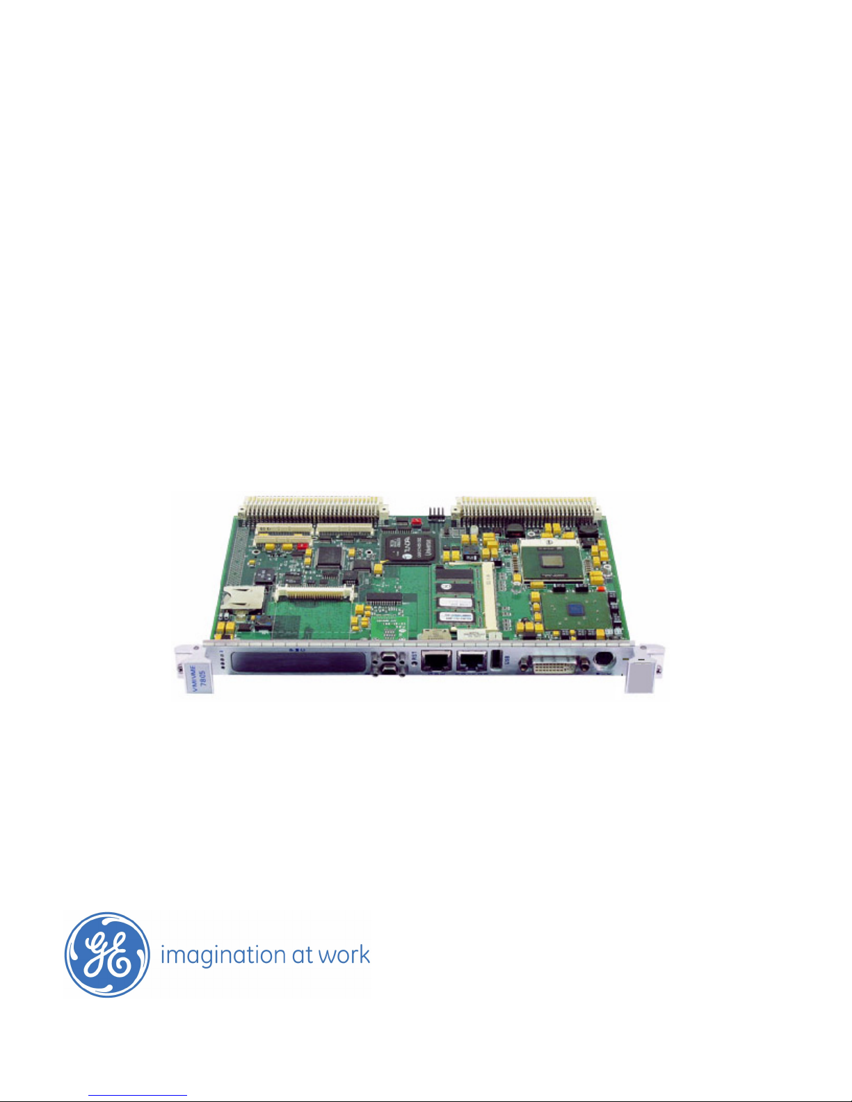
VMIVME-7805/VME-7805RC*
Intel® Pentium® 4 Processor M-Based VME Single Board Computer
THE VMIVME-7805 IS DESIGNED TO MEET THE EUROPEAN UNION (EU) RESTRICTIONS OF
HAZARDOUS SUBSTANCE (ROHS) DIRECTIVE (2002/95/EC) CURRENT REVISION.
Publication No: 500-007805-000 REV. E
Page 2

Document History
Hardware Reference Document Number: 500-007805-000 REV. E
February 21, 2013
Waste Electrical and Electronic Equipment (WEEE) Returns
GE is registered with an approved Producer Compliance Scheme (PCS) and, subject to suitable
contractual arrangements being in place, will ensure WEEE is processed in accordance with
the requirements of the WEEE Directive.
GE will evaluate requests to take back products purchased by our customers before
August 13, 2005 on a case by case basis. A WEEE management fee may apply.
Page 3

Table of Contents
List of Figures . . . . . . . . . . . . . . . . . . . . . . . . . . . . . . . . . . . . . . . . . . . . . . . . . . . . . . . . . . . . . . . . . . . . . . . . . . . . . . . . . . 5
List of Tables . . . . . . . . . . . . . . . . . . . . . . . . . . . . . . . . . . . . . . . . . . . . . . . . . . . . . . . . . . . . . . . . . . . . . . . . . . . . . . . . . . . 6
• Overview . . . . . . . . . . . . . . . . . . . . . . . . . . . . . . . . . . . . . . . . . . . . . . . . . . . . . . . . . . . . . . . . . . . . . . . . . . . . . . . . . . . . . 7
1 • Handling and Installation . . . . . . . . . . . . . . . . . . . . . . . . . . . . . . . . . . . . . . . . . . . . . . . . . . . . . . . . . . . . . . . . . . . 14
1.1 Unpacking Procedures. . . . . . . . . . . . . . . . . . . . . . . . . . . . . . . . . . . . . . . . . . . . . . . . . . . . . . . . . . . . . . . . . . . . . . . . . .14
1.2 Handling Precaution. . . . . . . . . . . . . . . . . . . . . . . . . . . . . . . . . . . . . . . . . . . . . . . . . . . . . . . . . . . . . . . . . . . . . . . . . . . .14
1.3 Hardware Setup. . . . . . . . . . . . . . . . . . . . . . . . . . . . . . . . . . . . . . . . . . . . . . . . . . . . . . . . . . . . . . . . . . . . . . . . . . . . . . . .14
1.3.1 CMOS Password . . . . . . . . . . . . . . . . . . . . . . . . . . . . . . . . . . . . . . . . . . . . . . . . . . . . . . . . . . . . . . . . . . . . . . . . . . .16
1.3.2 Power Requirements . . . . . . . . . . . . . . . . . . . . . . . . . . . . . . . . . . . . . . . . . . . . . . . . . . . . . . . . . . . . . . . . . . . . . . 17
1.4 Installation. . . . . . . . . . . . . . . . . . . . . . . . . . . . . . . . . . . . . . . . . . . . . . . . . . . . . . . . . . . . . . . . . . . . . . . . . . . . . . . . . . . . .18
1.5 Front/Rear Panel Connectors. . . . . . . . . . . . . . . . . . . . . . . . . . . . . . . . . . . . . . . . . . . . . . . . . . . . . . . . . . . . . . . . . . . .21
1.6 LED Definition. . . . . . . . . . . . . . . . . . . . . . . . . . . . . . . . . . . . . . . . . . . . . . . . . . . . . . . . . . . . . . . . . . . . . . . . . . . . . . . . . . .22
1.7 BIOS Setup. . . . . . . . . . . . . . . . . . . . . . . . . . . . . . . . . . . . . . . . . . . . . . . . . . . . . . . . . . . . . . . . . . . . . . . . . . . . . . . . . . . . .23
1.8 Battery Mounted in Horizontal Holder on the Board. . . . . . . . . . . . . . . . . . . . . . . . . . . . . . . . . . . . . . . . . . . . . . .24
2 • Standard Features . . . . . . . . . . . . . . . . . . . . . . . . . . . . . . . . . . . . . . . . . . . . . . . . . . . . . . . . . . . . . . . . . . . . . . . . .25
2.1 CPU. . . . . . . . . . . . . . . . . . . . . . . . . . . . . . . . . . . . . . . . . . . . . . . . . . . . . . . . . . . . . . . . . . . . . . . . . . . . . . . . . . . . . . . . . . . .25
2.2 Physical Memory. . . . . . . . . . . . . . . . . . . . . . . . . . . . . . . . . . . . . . . . . . . . . . . . . . . . . . . . . . . . . . . . . . . . . . . . . . . . . . . .26
2.3 Memory and Port Maps. . . . . . . . . . . . . . . . . . . . . . . . . . . . . . . . . . . . . . . . . . . . . . . . . . . . . . . . . . . . . . . . . . . . . . . . .27
2.3.1 Memory Map - Tundra Universe II-Based PCI-to-VME Bridge . . . . . . . . . . . . . . . . . . . . . . . . . . . . . . . . .27
2.4 I/O Port Map. . . . . . . . . . . . . . . . . . . . . . . . . . . . . . . . . . . . . . . . . . . . . . . . . . . . . . . . . . . . . . . . . . . . . . . . . . . . . . . . . . . .27
2.5 Interrupts. . . . . . . . . . . . . . . . . . . . . . . . . . . . . . . . . . . . . . . . . . . . . . . . . . . . . . . . . . . . . . . . . . . . . . . . . . . . . . . . . . . . . . .29
2.5.1 System Interrupts . . . . . . . . . . . . . . . . . . . . . . . . . . . . . . . . . . . . . . . . . . . . . . . . . . . . . . . . . . . . . . . . . . . . . . . . .29
2.5.2 PCI Interrupts . . . . . . . . . . . . . . . . . . . . . . . . . . . . . . . . . . . . . . . . . . . . . . . . . . . . . . . . . . . . . . . . . . . . . . . . . . . . .31
2.6 PCI Device Interrupt Map. . . . . . . . . . . . . . . . . . . . . . . . . . . . . . . . . . . . . . . . . . . . . . . . . . . . . . . . . . . . . . . . . . . . . . . .32
2.7 Integrated Peripherals. . . . . . . . . . . . . . . . . . . . . . . . . . . . . . . . . . . . . . . . . . . . . . . . . . . . . . . . . . . . . . . . . . . . . . . . . .34
2.8 Ethernet Controller. . . . . . . . . . . . . . . . . . . . . . . . . . . . . . . . . . . . . . . . . . . . . . . . . . . . . . . . . . . . . . . . . . . . . . . . . . . . . .35
2.9 Video Graphics Adapter. . . . . . . . . . . . . . . . . . . . . . . . . . . . . . . . . . . . . . . . . . . . . . . . . . . . . . . . . . . . . . . . . . . . . . . . .36
2.9.1 Digital Video Interface (DVI) . . . . . . . . . . . . . . . . . . . . . . . . . . . . . . . . . . . . . . . . . . . . . . . . . . . . . . . . . . . . . . . .37
2.9.2 DVI Connectors . . . . . . . . . . . . . . . . . . . . . . . . . . . . . . . . . . . . . . . . . . . . . . . . . . . . . . . . . . . . . . . . . . . . . . . . . . . .37
2.10 Universal Serial Bus. . . . . . . . . . . . . . . . . . . . . . . . . . . . . . . . . . . . . . . . . . . . . . . . . . . . . . . . . . . . . . . . . . . . . . . . . . . .38
3 • Embedded PC/RTOS Features . . . . . . . . . . . . . . . . . . . . . . . . . . . . . . . . . . . . . . . . . . . . . . . . . . . . . . . . . . . . . . .39
3.1 VME Bridge. . . . . . . . . . . . . . . . . . . . . . . . . . . . . . . . . . . . . . . . . . . . . . . . . . . . . . . . . . . . . . . . . . . . . . . . . . . . . . . . . . . . .39
3.2 I2C Support. . . . . . . . . . . . . . . . . . . . . . . . . . . . . . . . . . . . . . . . . . . . . . . . . . . . . . . . . . . . . . . . . . . . . . . . . . . . . . . . . . . . .40
3.3 Embedded PCI Functions. . . . . . . . . . . . . . . . . . . . . . . . . . . . . . . . . . . . . . . . . . . . . . . . . . . . . . . . . . . . . . . . . . . . . . . .41
3.4 Timers. . . . . . . . . . . . . . . . . . . . . . . . . . . . . . . . . . . . . . . . . . . . . . . . . . . . . . . . . . . . . . . . . . . . . . . . . . . . . . . . . . . . . . . . . .42
3.4.1 General . . . . . . . . . . . . . . . . . . . . . . . . . . . . . . . . . . . . . . . . . . . . . . . . . . . . . . . . . . . . . . . . . . . . . . . . . . . . . . . . . . .42
3.4.2 Timer Control Status Register 1 (TCSR1) . . . . . . . . . . . . . . . . . . . . . . . . . . . . . . . . . . . . . . . . . . . . . . . . . . . . .42
3.4.3 Timer Control Status Register 2 (TCSR2) . . . . . . . . . . . . . . . . . . . . . . . . . . . . . . . . . . . . . . . . . . . . . . . . . . . . .43
3.4.4 Timer 1 & 2 Load Count Register (TMRLCR12) . . . . . . . . . . . . . . . . . . . . . . . . . . . . . . . . . . . . . . . . . . . . . . . . 43
3.4.5 Timer 3 Load Count Register (TMRLCR3) . . . . . . . . . . . . . . . . . . . . . . . . . . . . . . . . . . . . . . . . . . . . . . . . . . . .44
3.4.6 Timer 4 Load Count Register (TMRLCR4) . . . . . . . . . . . . . . . . . . . . . . . . . . . . . . . . . . . . . . . . . . . . . . . . . . . .44
Table of Contents 3
Page 4

3.4.7 Timer 1 & 2 Current Count Register (TMRCCR12) . . . . . . . . . . . . . . . . . . . . . . . . . . . . . . . . . . . . . . . . . . . . .44
3.4.8 Timer 3 Current Count Register (TMRCCR3) . . . . . . . . . . . . . . . . . . . . . . . . . . . . . . . . . . . . . . . . . . . . . . . . . .44
3.4.9 Timer 4 Current Count Register (TMRCCR4) . . . . . . . . . . . . . . . . . . . . . . . . . . . . . . . . . . . . . . . . . . . . . . . . . .45
3.4.10 Timer 1 IRQ Clear (T1IC) . . . . . . . . . . . . . . . . . . . . . . . . . . . . . . . . . . . . . . . . . . . . . . . . . . . . . . . . . . . . . . . . . . .45
3.4.11 Timer 2 IRQ Clear (T2IC) . . . . . . . . . . . . . . . . . . . . . . . . . . . . . . . . . . . . . . . . . . . . . . . . . . . . . . . . . . . . . . . . . . .45
3.4.12 Timer 3 IRQ Clear (T3IC) . . . . . . . . . . . . . . . . . . . . . . . . . . . . . . . . . . . . . . . . . . . . . . . . . . . . . . . . . . . . . . . . . . .45
3.4.13 Timer 4 IRQ Clear (T4IC) . . . . . . . . . . . . . . . . . . . . . . . . . . . . . . . . . . . . . . . . . . . . . . . . . . . . . . . . . . . . . . . . . . .45
3.5 Watchdog Timer. . . . . . . . . . . . . . . . . . . . . . . . . . . . . . . . . . . . . . . . . . . . . . . . . . . . . . . . . . . . . . . . . . . . . . . . . . . . . . . .46
3.5.1 General . . . . . . . . . . . . . . . . . . . . . . . . . . . . . . . . . . . . . . . . . . . . . . . . . . . . . . . . . . . . . . . . . . . . . . . . . . . . . . . . . . .46
3.5.2 WDT Control Status Register (WCSR) . . . . . . . . . . . . . . . . . . . . . . . . . . . . . . . . . . . . . . . . . . . . . . . . . . . . . . . .46
3.5.3 WDT Keepalive Register (WKPA) . . . . . . . . . . . . . . . . . . . . . . . . . . . . . . . . . . . . . . . . . . . . . . . . . . . . . . . . . . . .46
3.6 NVRAM. . . . . . . . . . . . . . . . . . . . . . . . . . . . . . . . . . . . . . . . . . . . . . . . . . . . . . . . . . . . . . . . . . . . . . . . . . . . . . . . . . . . . . . . .47
3.7 VME Control. . . . . . . . . . . . . . . . . . . . . . . . . . . . . . . . . . . . . . . . . . . . . . . . . . . . . . . . . . . . . . . . . . . . . . . . . . . . . . . . . . . .47
3.8 CompactFlash. . . . . . . . . . . . . . . . . . . . . . . . . . . . . . . . . . . . . . . . . . . . . . . . . . . . . . . . . . . . . . . . . . . . . . . . . . . . . . . . . .48
3.9 Remote Ethernet Booting. . . . . . . . . . . . . . . . . . . . . . . . . . . . . . . . . . . . . . . . . . . . . . . . . . . . . . . . . . . . . . . . . . . . . . . .48
3.9.1 BootWare Features: . . . . . . . . . . . . . . . . . . . . . . . . . . . . . . . . . . . . . . . . . . . . . . . . . . . . . . . . . . . . . . . . . . . . . . . 48
Maintenance. . . . . . . . . . . . . . . . . . . . . . . . . . . . . . . . . . . . . . . . . . . . . . . . . . . . . . . . . . . . . . . . . . . . . . . . . . . . . . . . . .49
Compliance Information . . . . . . . . . . . . . . . . . . . . . . . . . . . . . . . . . . . . . . . . . . . . . . . . . . . . . . . . . . . . . . . . . . . . . . .50
A • Appendix A: Connectors and Pinouts . . . . . . . . . . . . . . . . . . . . . . . . . . . . . . . . . . . . . . . . . . . . . . . . . . . . . . . 52
B • Appendix B: AMI BIOS Setup Utility . . . . . . . . . . . . . . . . . . . . . . . . . . . . . . . . . . . . . . . . . . . . . . . . . . . . . . . . . 62
C • Appendix C: OS and System Driver Software . . . . . . . . . . . . . . . . . . . . . . . . . . . . . . . . . . . . . . . . . . . . . . . . 70
D • Appendix D: Argon BIOS . . . . . . . . . . . . . . . . . . . . . . . . . . . . . . . . . . . . . . . . . . . . . . . . . . . . . . . . . . . . . . . . . . . 76
E • Appendix E: Sample C Software . . . . . . . . . . . . . . . . . . . . . . . . . . . . . . . . . . . . . . . . . . . . . . . . . . . . . . . . . . . . 80
4 4 VMIVME-7805/VME-7805RC Hardware Reference Manual
Page 5

List of Figures
Figure 1 VMIVME-7805/VME-7805RC Block Diagram . . . . . . . . . . . . . . . . . . . . . . . . . . . . . . . . . . . . . . . . . . . . . . . . . . . . . 9
Figure 1-1 VMIVME-7805/VME-7805RC Board Layout. . . . . . . . . . . . . . . . . . . . . . . . . . . . . . . . . . . . . . . . . . . . . . . . . . . . 15
Figure 1-2 Installing a PMC Card on the VMIVME-7805/VME-7805RC . . . . . . . . . . . . . . . . . . . . . . . . . . . . . . . . . . . . .19
Figure 1-3 Backside Mounting for the VMIVME-7805/VME-7805RC PMC Site . . . . . . . . . . . . . . . . . . . . . . . . . . . . . .20
Figure 1-4 Front Panel LED Positions . . . . . . . . . . . . . . . . . . . . . . . . . . . . . . . . . . . . . . . . . . . . . . . . . . . . . . . . . . . . . . . . . . . .22
Figure 1-5 Battery Location, Top of Assembly . . . . . . . . . . . . . . . . . . . . . . . . . . . . . . . . . . . . . . . . . . . . . . . . . . . . . . . . . . . .24
Figure 1-6 Battery Removal . . . . . . . . . . . . . . . . . . . . . . . . . . . . . . . . . . . . . . . . . . . . . . . . . . . . . . . . . . . . . . . . . . . . . . . . . . . . .24
Figure 2-1 Connections for the PC Interrupt Logic Controller . . . . . . . . . . . . . . . . . . . . . . . . . . . . . . . . . . . . . . . . . . . . .33
Figure A-1 VME Connector Diagram . . . . . . . . . . . . . . . . . . . . . . . . . . . . . . . . . . . . . . . . . . . . . . . . . . . . . . . . . . . . . . . . . . . .52
Figure A-2 Serial Connector Pinouts . . . . . . . . . . . . . . . . . . . . . . . . . . . . . . . . . . . . . . . . . . . . . . . . . . . . . . . . . . . . . . . . . . . .54
Figure A-3 USB Connector Pinout . . . . . . . . . . . . . . . . . . . . . . . . . . . . . . . . . . . . . . . . . . . . . . . . . . . . . . . . . . . . . . . . . . . . . . .54
Figure A-4 10/100 Mbit Ethernet Connector (J14) and Pinout . . . . . . . . . . . . . . . . . . . . . . . . . . . . . . . . . . . . . . . . . . . . .55
Figure A-5 Gigabit Ethernet Connector (J15) and Pinout . . . . . . . . . . . . . . . . . . . . . . . . . . . . . . . . . . . . . . . . . . . . . . . . . .55
Figure A-6 DVI-I Connector and DVI-I-to-SVGA Adapter . . . . . . . . . . . . . . . . . . . . . . . . . . . . . . . . . . . . . . . . . . . . . . . . . .56
Figure A-7 Keyboard/Mouse Connector and Pinout . . . . . . . . . . . . . . . . . . . . . . . . . . . . . . . . . . . . . . . . . . . . . . . . . . . . . .57
Figure A-8 Mouse/Keyboard Y Splitter Cable . . . . . . . . . . . . . . . . . . . . . . . . . . . . . . . . . . . . . . . . . . . . . . . . . . . . . . . . . . . .58
List of Figures 5
Page 6

List of Tables
Table 1-1 VMIVME-7805/VME-7805RC Headers, Jumpers and Connectors . . . . . . . . . . . . . . . . . . . . . . . . . . . . . . . . .16
Table 1-2 Clear CMOS (User Configurable) - Jumper (E3) . . . . . . . . . . . . . . . . . . . . . . . . . . . . . . . . . . . . . . . . . . . . . . . . . .16
Table 1-3 Boot Continuation - Jumper (E11) . . . . . . . . . . . . . . . . . . . . . . . . . . . . . . . . . . . . . . . . . . . . . . . . . . . . . . . . . . . . . .16
Table 1-4 VME SYSRESET Enable/Disable (User Configurable) - Switch (S6) . . . . . . . . . . . . . . . . . . . . . . . . . . . . . . . . .17
Table 1-5 Universe II Mapping/SYSFAIL Generation (User Configurable) - Switch (S7) . . . . . . . . . . . . . . . . . . . . . . .17
Table 1-6 Status Indications . . . . . . . . . . . . . . . . . . . . . . . . . . . . . . . . . . . . . . . . . . . . . . . . . . . . . . . . . . . . . . . . . . . . . . . . . . . .23
Table 2-1 VMIVME-7805/VME-7805RC, Universe II-Based Interface Memory Address Map . . . . . . . . . . . . . . . . .27
Table 2-2 VMIVME-7805/VME-7805RC I/O Address Map . . . . . . . . . . . . . . . . . . . . . . . . . . . . . . . . . . . . . . . . . . . . . . . . . .28
Table 2-3 Interrupt Line Assignments . . . . . . . . . . . . . . . . . . . . . . . . . . . . . . . . . . . . . . . . . . . . . . . . . . . . . . . . . . . . . . . . . . . .29
Table 2-4 Interrupt Vector Table . . . . . . . . . . . . . . . . . . . . . . . . . . . . . . . . . . . . . . . . . . . . . . . . . . . . . . . . . . . . . . . . . . . . . . . .30
Table 2-5 PCI Device Interrupt Mapping by the BIOS . . . . . . . . . . . . . . . . . . . . . . . . . . . . . . . . . . . . . . . . . . . . . . . . . . . . .32
Table 2-6 NMI Register Bit Descriptions . . . . . . . . . . . . . . . . . . . . . . . . . . . . . . . . . . . . . . . . . . . . . . . . . . . . . . . . . . . . . . . . . .34
Table 2-7 Partial List of Display Modes Supported . . . . . . . . . . . . . . . . . . . . . . . . . . . . . . . . . . . . . . . . . . . . . . . . . . . . . . . .36
Table 3-1 I2Cbus Through E12 . . . . . . . . . . . . . . . . . . . . . . . . . . . . . . . . . . . . . . . . . . . . . . . . . . . . . . . . . . . . . . . . . . . . . . . . . . .40
Table 3-2 PCI Configuration Space Registers . . . . . . . . . . . . . . . . . . . . . . . . . . . . . . . . . . . . . . . . . . . . . . . . . . . . . . . . . . . . .41
Table 3-3 Register Definitions Offset From BAR0 . . . . . . . . . . . . . . . . . . . . . . . . . . . . . . . . . . . . . . . . . . . . . . . . . . . . . . . . .47
Table A-1 VME Connector Pinout. . . . . . . . . . . . . . . . . . . . . . . . . . . . . . . . . . . . . . . . . . . . . . . . . . . . . . . . . . . . . . . . . . . . . . . . .52
Table A-2 DVI-I Connector Pinout . . . . . . . . . . . . . . . . . . . . . . . . . . . . . . . . . . . . . . . . . . . . . . . . . . . . . . . . . . . . . . . . . . . . . . .56
Table A-3 Keyboard/Mouse Y Splitter Cable . . . . . . . . . . . . . . . . . . . . . . . . . . . . . . . . . . . . . . . . . . . . . . . . . . . . . . . . . . . . . .58
Table A-4 PMC #1 (J1) Connector Pinout . . . . . . . . . . . . . . . . . . . . . . . . . . . . . . . . . . . . . . . . . . . . . . . . . . . . . . . . . . . . . . . . .59
Table A-5 PMC #1 (J2) Connector Pinout . . . . . . . . . . . . . . . . . . . . . . . . . . . . . . . . . . . . . . . . . . . . . . . . . . . . . . . . . . . . . . . . .60
Table A-6 PMC #1 (J3) Connector Pinout . . . . . . . . . . . . . . . . . . . . . . . . . . . . . . . . . . . . . . . . . . . . . . . . . . . . . . . . . . . . . . . . .61
6 VMIVME-7805/VME-7805RC Hardware Reference Manual
Page 7

• Overview
The VMIVME-7805/VME-7805RC* are full featured Pentium® 4 Processor - M
compatible Single Board Computers (SBCs) in a single-slot, passively cooled,
Eurocard form factor that utilizes the advanced technology of Intel
®
’s 852GM
chipset running a front-side bus rate of 400 MHz. The VMIVME-7805/
VME-7805RC are compliant with the VMEbus Specification Rev. C.1 and features
a transparent PCI-to-VME bridge, allowing the board to function as a system
controller or peripheral CPU in multi-CPU systems.
The VMIVME-7805/VME-7805RC provide features typically found on desktop
systems such as:
• Up to 1 GByte PC1600 DDR SDRAM
• Internal SVGA and DVI controller
• Two built-in Ethernet controllers
• IDE drive support (VME P2)
• Floppy drive support (VME P2)
• Two high performance 16550-compatible serial ports (COM1 and COM2)
• Front panel Universal Serial Bus (USB ) connection Rev. 2.0
• Real-Time clock/calendar
• Front panel reset switch
• Miniature speaker
• Keyboard/Mouse port
The VMIVME-7805/VME-7805RC are capable of executing many of today’s
desktop operating systems such as Microsoft
®
and a wide variety of Linux
-based operating systems. The standard desktop
®
’s Windows® XP, Windows 2000,
features of the VMIVME-7805/VME-7805RC are described in Chapter 2 Standard
Features, page 25 of this manual.
The VMIVME-7805/VME-7805RC provide features useful to embedded
applications such as:
2
C bus support
• I
• Remote Ethernet booting
• Up to 1 GByte of CompactFlash (optional)
• Four general-purpose programmable timers (two 16-bit and two 32-bit)
• Software-selectable Watchdog Timer with reset
• 32 KByte Nonvolatile RAM
Additionally, the VMIVME-7805/VME-7805RC offer a PMC expansion site with
front-panel access. The VMIVME-7805/VME-7805RC are capable of executing
many of today’s embedded operating systems such as VxWorks
LynxOS
®
and Microsoft’s Windows XP. The embedded features of the
®
, QNX®, Linux®,
VMIVME-7805/ VME-7805RC are described in Chapter 3 Embedded PC/RTOS
Features, page 39 of this manual.
Overview 7
Page 8

The VMIVME-7805/VME-7805RC are suitable for use in a variety of applications,
such as: telecommunications, simulation, instrumentation, industrial control,
process control and monitoring, factory automation, automated test systems, data
acquisition systems and anywhere that the highest performance processing
power in a single VME slot is desired.
Intel 852GM Chipset
The VMIVME-7805/VME-7805RC incorporate the latest Intel chipset technology,
the 852GM. The Intel 852GM chipset is an optimized integrated graphics solution
with a 400 MHz system bus and integrated 32-bit 3D core at 133 MHz with
dynamic video memory technology (DVMT). The chipset has a low power design,
advanced power management, supporting up to 1 GByte of DDR system Memory.
The 852GM is a Graphics Memory Controller Hub component (GMCH),
providing the processor interface, system memory interface (DDR SDRAM), Hub
interface, CRT and digital video out (DVO) port.
Key features for the 852GM:
• 400 MHz Processor system bus controller
• Graphics controller interface
• One digital video out port
• Supports DDR200 memory technology
• High-speed accelerated hub architecture interface for communication with
the ICH4-M (I/O controller)
8 VMIVME-7805/VME-7805RC Hardware Reference Manual
Page 9
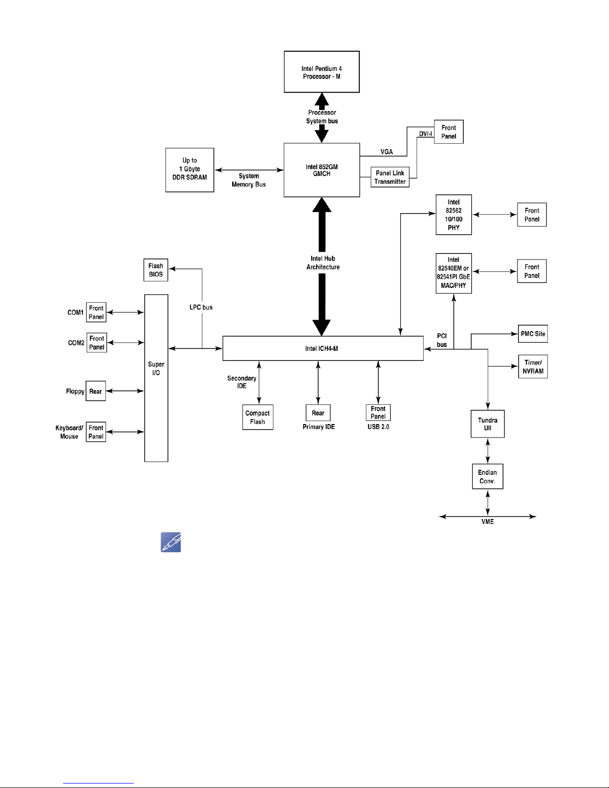
Figure 1 VMIVME-7805/VME-7805RC Block Diagram
NOTE
Intel 82540EM is used on VMIVME-7805 and Intel 82541PI is used on VME-7805RC (RoHS).
Overview 9
Page 10

Organization
This manual is composed of the following chapters and appendices:
Overview provides a general description of the VMIVME-7805/VME-7805RC and
General Safety terms and symbols.
Chapter 1 Handling and Installation describes unpacking, inspection, hardware
jumper settings, connector definitions, installation, system setup and operation of
the VMIVME-7805/VME-7805RC.
Chapter 2 Standard Features describes the unit design in terms of the standard PC
memory and I/O maps, along with the standard interrupt architecture.
Chapter 3 - Embedded PC/RTOS Features describes the unit features that are
beyond standard functions.
Maintenance provides GE contact information relative to the care and
maintenance of the unit.
Compliance provides applicable information regarding regulatory compliance.
Appendix A Connector Pinouts illustrates and defines the connectors included in
the unit’s I/O ports.
Appendix B - AMI BIOS describes the menus and options associated with the
American Megatrends, Inc. (system) BIOS.
Appendix C - System Driver Software provides details for installing drivers under
Windows 2000 and Windows XP.
Appendix D - Argon BIOS describes the menus and options associated with the
remote Ethernet booting BIOS.
Appendix E - Sample C Software provides listings of a library of sample code that
the programmer may utilize to build applications.
10 VMIVME-7805/VME-7805RC Hardware Reference Manual
Page 11

References
Pentium 4 Processor-M μFCPGA package at 1.7 to 2.2GHz
January 2003, Order Number 250686-005
Intel 852GM Graphics and Memory Controller Hub (GMCH)
January 2003, Order Number 252338-001
Intel 82801DBM I/O Controller Hub 4 Mobile (ICH4-M)
January 2003, Order Number 252337-001
Intel 82540EM Gigabit Ethernet Controller
April 2003
PCI Local Bus Specification, Rev. 2.1
PCI Special Interest Group
P.O. Box 14070
Portland, OR 97214
(800) 433-5177 (U.S.)
(503) 797-4207 (International)
(503) 234-6762 (FAX)
CMC Specification, P1386/Draft 2.0 from:
IEEE Standards Department
Copyrights and Permissions
445 Hoes Lanes, P.O. Box 1331
Piscataway, NJ 08855-1331, USA
PMC Specification, P1386.1/Draft 2.0 from:
IEEE Standards Department
Copyrights and Permissions
445 Hoes Lanes, P.O. Box 1331
Piscataway, NJ 08855-1331, USA
VMISFT-9420 IOWorks Access User’s Guide
Doc. No. 520-009420-910
GE Intelligent Platforms
12090 South Memorial Pkwy.
Huntsville, AL 35803-3308
(800) 322-3616
www.ge-ip.com
Tundra Universe II Based VMEbus Interface
Doc. No. 500-000211-000
GE Intelligent Platforms
12090 South Memorial Pkwy.
Huntsville, AL 35803-3308
(800) 322-3616
www.ge-ip.com
For a detailed description and specification of the VMEbus, please refer to:
VMEbus Specification Rev. C. and the VMEbus Handbook
VMEbus International Trade Assoc. (VITA)
7825 East Gelding Dr.
Suite 104
Scottsdale, AZ 85260
(602) 951-8866
(602) 951-0720 (FAX)
www.vita.com
Overview 11
Page 12

Safety Summary
The following general safety precautions must be observed during all phases of
the operation, service and repair of this product. Failure to comply with these
precautions or with specific warnings elsewhere in this manual violates safety
standards of design, manufacture and intended use of this product.
GE assumes no liability for the customer's failure to comply with these
requirements.
Ground the
System
Do Not Operate in
an Explosive
Atmosphere
Keep Away from
Live Circuits
Do Not Service or
Adjust Alone
Do Not Substitute
Parts or Modify
System
Dangerous
Procedure
Warnings
To minimize shock hazard, the chassis and system cabinet must be connected to
an electrical ground. A three-conductor AC power cable should be used. The
power cable must either be plugged into an approved three-contact electrical
outlet or used with a three-contact to two-contact adapter with the grounding
wire (green) firmly connected to an electrical ground (safety ground) at the power
outlet.
Do not operate the system in the presence of flammable gases or fumes. Operation
of any electrical system in such an environment constitutes a definite safety
hazard.
Operating personnel must not remove product covers. Component replacement
and internal adjustments must be made by qualified maintenance personnel. Do
not replace components with power cable connected. Under certain conditions,
dangerous voltages may exist even with the power cable removed. To avoid
injuries, always disconnect power and discharge circuits before touching them.
Do not attempt internal service or adjustment unless another person capable of
rendering first aid and resuscitation is present.
Because of the danger of introducing additional hazards, do not install substitute
parts or perform any unauthorized modification to the product. Return the
product to GE for service and repair to ensure that safety features are maintained.
Warnings, such as the example below, precede only potentially dangerous
procedures throughout this manual. Instructions contained in the warnings must
be followed.
WARNING
Dangerous voltages, capable of causing death, are present in this system.
Use extreme caution when handling, testing and adjusting.
12 VMIVME-7805/VME-7805RC Hardware Reference Manual
Page 13

Warnings,
Cautions
and Notes
WARNING
WARNING denotes a hazard. It calls attention to a procedure, practice, or
condition, which, if not correctly performed or adhered to, could result in
injury or death to personnel.
CAUTION
CAUTION denotes a hazard. It calls attention to an operating procedure,
practice, or condition, which, if not correctly performed or adhered to, could
result in damage to or destruction of part or all of the system.
NOTE
NOTE denotes important information. It calls attention to a procedure, practice, or condition which
is essential to highlight.
TIP
Tip denotes a bit of expert information.
LINK
This is link text.
Overview 13
Page 14

1 • Handling and Installation
This chapter describes the hardware jumper settings, connector descriptions,
installation, system setup and operation of the VMIVME-7805/VME-7805RC.
1.1 Unpacking Procedures
Any precautions found in the shipping container should be observed. All items
should be carefully unpacked and thoroughly inspected for damage that might
have occurred during shipment. The board(s) should be checked for broken
components, damaged printed circuit board(s), heat damage and other visible
contamination. All claims arising from shipping damage should be filed with the
carrier and a complete report sent to GE Customer Care.
1.2 Handling Precaution
Electronic assemblies use devices that are sensitive to static discharge. Observe
anti-static procedures when handling these boards. All products should be in an
anti-static plastic bag or conductive foam for storage or shipment. Work at an
approved anti-static workstation when unpacking boards.
1.3 Hardware Setup
The VMIVME-7805/VME-7805RC are factory populated with user-specified
options as part of the VMIVME-7805/VME-7805RC ordering information. The
processor speed, memory size and CompactFlash memory size are not userupgradable. To change processor speeds or RAM/Flash size, contact Customer
Care to receive a Return Material Authorization (RMA).
GE Customer Care is available at: 1-800-433-2682 in North America,
or +1-780-401-7700 for international calls. Or, visit our website www.ge-ip.com.
The VMIVME-7805/VME-7805RC are tested for system operation and shipped
with factory-installed header jumpers. The physical location of the jumpers and
connectors for the SBC are illustrated in Figure 1-1 on page 15. The definitions of
the SBC jumpers and connectors are included in Table 1-1 through Table 1-5.
CAUTION
All jumpers marked User Configurable in the following tables may be changed
or modified by the user. All jumpers marked Factory Configured should not be
modified by the user.
Care must be taken when making jumper modifications to ensure against
improper settings or connections. Improper settings may result in damage to
the unit. Modifying any jumper not marked User Configurable will void the
Warranty and may damage the unit. The default jumper condition of the
VMIVME-7805/VME-7805RC are expressed in Table 1-1 through Table 1-5 with
bold text
in the table cells.
14 VMIVME-7805/VME-7805RC Hardware Reference Manual
Page 15
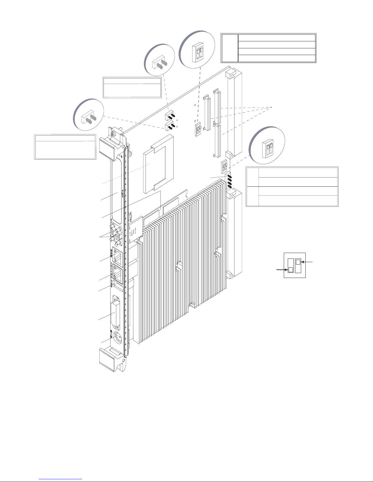
Figure 1-1 VMIVME-7805/VME-7805RC Board Layout
E3
E3
CMOS Clear
Momentarily short the pins of E3
for approximately five seconds.
S6
3
4
2
1
Shown in the factory
default state.
S6
Pins 1 - 4: Open - Disable VMEbus SYSRST Driver
Pins 1 - 4: Closed - Enable VMEbus SYSRST Driver (D)
Pins 2 - 3: Open - Disable SYSRST Receiver
VMEbus
SYSRESET
Pins 2 - 3: Closed - Enable SYSRST Receiver (D)
Enable/Disable
(D) Denotes: Default State.
E11
E11
Boot Continuation Jumper
Install a shunt on Jumper E11
to load default settings and to
continue booting on a CMOS error.
CompactFlash
PMC Site
1 and 2 (J17)
Gigabit
Ethernet (J15)
Mbit (J14)
USB Port
VMIVME
Memory
Module
COM
10/100
(J12)
7805
E3
E11
P6
J2
S6
E12
2
I C
S7
J1
J3
P1
P2
PMC Site
Connectors
S7
2
Shown in the factory
1
default state.
4
3
Pins 1 - 4: Open - Map Universe II in Memory Space (D)
Mapping
Pins 1 - 4: Closed - Map Universe II to I/O Space
Universe II
Pins 2 - 3: Open - Disable SYSFAIL Generation (D)
Pins 2 - 3: Closed - Enable SYSFAIL Generation
SYSFAIL
Generation
(D) Denotes: Default State.
NOTE: When the switch is in the
down position, it is open.
When the switch is in the
up position, it is closed.
DOWN
(Open)
S7
Switch Example:
43
(Closed)
12
UP
DVI
Connector (J10)
Mouse/
Keyboard (J16)
Handling and Installation 15
Page 16

Table 1-1 VMIVME-7805/VME-7805RC Headers, Jumpers and Connectors
Connector Function
J16 Mouse/Keyboard
J15 10/100/1000 GbE
J14 10/100 Mbit Ethernet
P2 IDE (Primary), Floppy
J12 USB port
J10 DVI Video
E10, E18, E19 Factory Reserved Do Not Use
E3 CMOS Clear Jumper
E11 Boot Continuation Jumper
2
E12 I
S6, S7 VME Switches
J1, J2, J3 PMC Site Connectors
P6 CompactFlash Connector
S8 Factory Configured (Default is ON)
J17 COM 1, COM 2
P1, P2 VME Backplane Connectors
C Header
NOTE
The BIOS has the capability (not currently enabled) of password protecting casual access to the
unit’s CMOS set-up screens. The CMOS Clear jumper allows the user to clear the password in the
case of a forgotten password.
1.3.1 CMOS Password
To clear the CMOS password:
1. Turn off power to the unit.
2. Momentarily short the pins of E3 for approximately five seconds.
3. Power up the unit.
When power is reapplied to the unit, the CMOS password will be cleared.
Table 1-2 Clear CMOS (User Configurable) - Jumper (E3)
Select Jumper Position
Normal Open
Clear CMOS/Password Momentarily Short
Table 1-3 Boot Continuation - Jumper (E11)
Select Jumper Position
Load Default settings and
continue booting on CMOS
error
Stop booting on CMOS error Out
In
16 VMIVME-7805/VME-7805RC Hardware Reference Manual
Page 17

Table 1-4 VME SYSRESET Enable/Disable (User Configurable) - Switch (S6)
Select Switch Position Switch No.
Disable VME SYSRST Driver Open 1 - 4
Enable VME SYSRST Driver Closed 1 - 4
Disable VME SYSRST Receiver Open 2 - 3
Enable SYSRST Receiver Closed 2 - 3
Table 1-5 Universe II Mapping/SYSFAIL Generation (User Configurable) - Switch (S7)
Select Switch Position Switch No.
Map UNIV2 to Memory Space Open 1-4
Map UNIV2 to I/O Space Closed 1-4
Disable SYSFAIL Generation Open 2-3
Enable SYSFAIL Generation Closed 2-3
1.3.2 Power Requirements
The VMIVME-7805/VME-7805RC require +5 V from the VME backplane. Below
are the voltage and current requirements.
Supply Current (Typical) Current (Maximum)
+5V 6.08A 8.2A
The VMIVME-7805/VME-7805RC provide power to the PMC site in accordance
with the PMC specification. The maximum current provided on the +5 V supply is
1.5 A per PMC site. The maximum current provided on the +3.3 V supply is 1.5 A
per PMC site.
Handling and Installation 17
Page 18

1.4 Installation
The VMIVME-7805/VME-7805RC conform to the VME physical specification for a
single slot 6U Eurocard (dual height). It can be plugged directly into any standard
chassis accepting this type of board.
CAUTION
Do not install or remove the board while power is applied.
The following steps describe the GE recommended method for VMIVME-7805/
VME-7805RC installation and power-up:
1. Make sure power to the equipment is off.
2. Choose chassis slot. The VMIVME-7805/VME-7805RC must be attached to a
P1/P2 VME backplane.
If the VMIVME-7805/VME-7805RC are to be the VME system controller,
choose the first VME slot. If a different board is the VME system controller,
choose any slot except slot one. The VMIVME-7805/VME-7805RC do not
require jumpers for enabling/disabling the system controller function.
NOTE
Air flow requirements as measured at output side of heatsink is to be greater than 350LFM.
3. Connect all needed peripherals to the front panel. Each connector is clearly
labeled on the front panel, and detailed pinouts are in Appendix A: Connec-
tors and Pinouts, page 52. Minimally, a keyboard and a monitor are required
if the user has not previously configured the system.
4. Apply power to the system. Several messages are displayed on the screen,
including names, versions and copyright dates for the various BIOS modules
on the VMIVME-7805/VME-7805RC.
5. The VMIVME-7805/VME-7805RC feature an optional CompactFlash resident
on the board. Refer to Chapter 3 Embedded PC/RTOS Features, page 39 for
set up details.
6. If an external drive module is installed, the BIOS Setup program must be run
to configure the drive types. See Appendix B: AMI BIOS Setup Utility,
page 62 to properly configure the system.
7. If a drive module is present, install the operating system according to the
manufacturer’s instructions.
See Appendix C: OS and System Driver Software, page 70 for instructions on
installing VMIVME-7805/VME-7805RC peripheral driver software during
operating system installation.
18 VMIVME-7805/VME-7805RC Hardware Reference Manual
Page 19
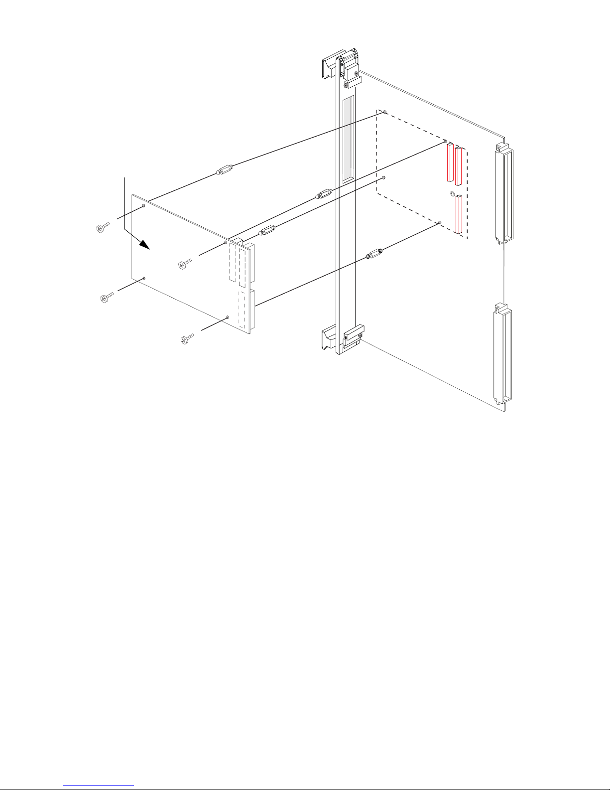
Figure 1-2 Installing a PMC Card on the VMIVME-7805/VME-7805RC
Third Party
PMC Expansion Board
Handling and Installation 19
Page 20
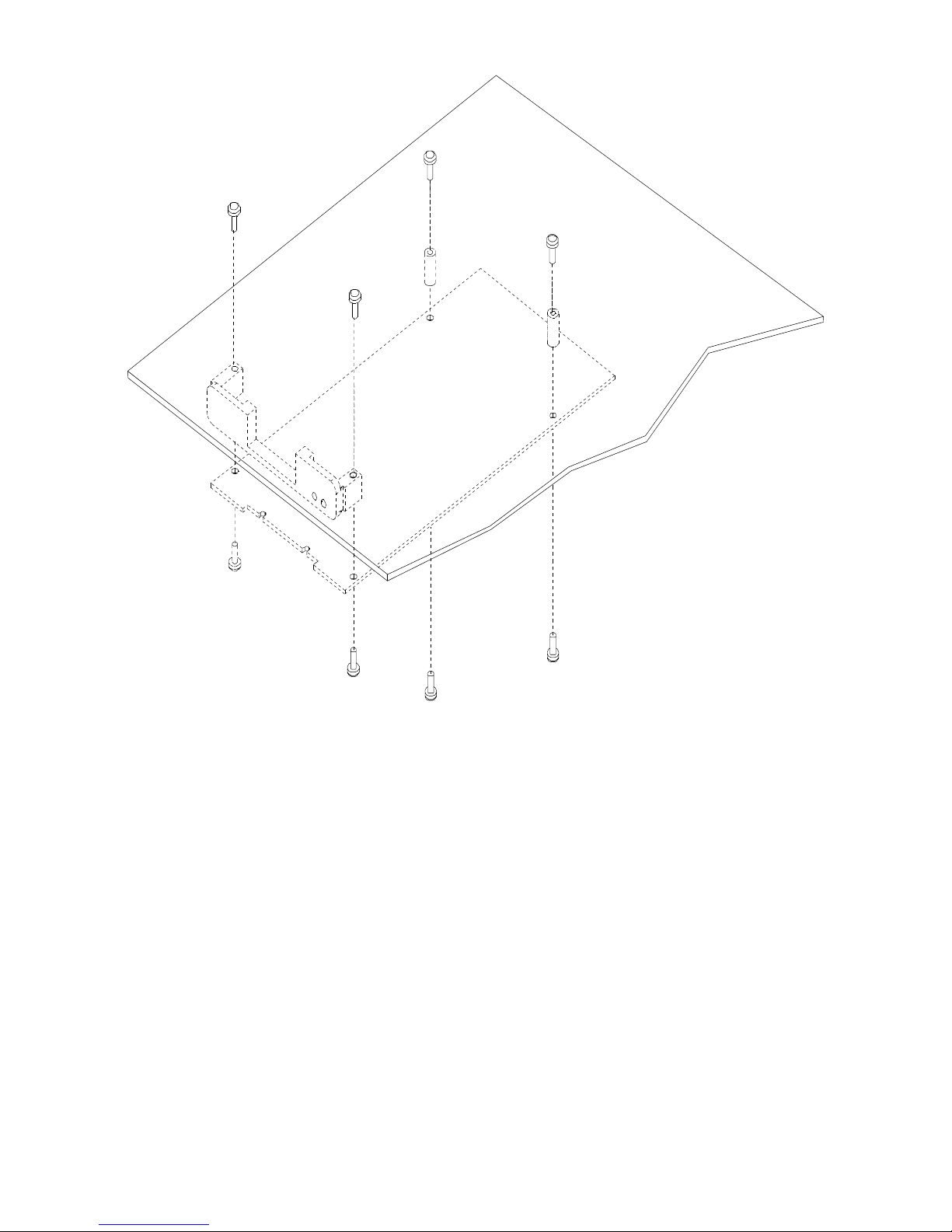
Figure 1-3 Backside Mounting for the VMIVME-7805/VME-7805RC PMC Site
B
a
c
k
o
f
VM
(
So
805 SBC
(Solder Side)
Back of VMIVME-7
I
V
M
E-
7
l
d
8
e
0
r
5
S
/
V
i
d
M
e
E-
)
7
8
0
5
R
C
SB
C
20 VMIVME-7805/VME-7805RC Hardware Reference Manual
Page 21

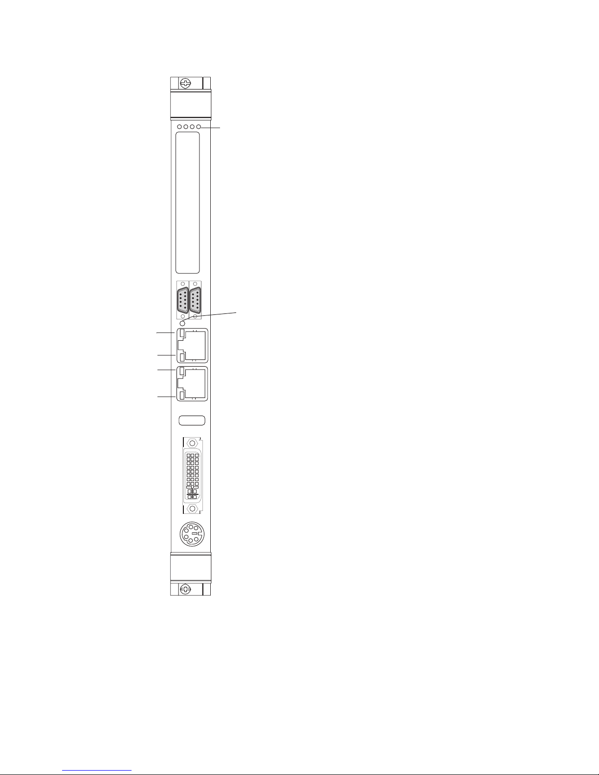
1.5 Front/Rear Panel Connectors
The VMIVME-7805/VME-7805RC provide front panel access to the PMC
expansion site, the DVI connector, the 10/100 and Gigabit Ethernet (GbE)
connectors, the manual reset switch, COM ports 1 and 2, one USB port and the
status LEDs. A drawing of the VMIVME-7805/VME-7805RC front panel is shown
in Figure 1-4. The front panel connectors and indicators are labeled as follows:
• GBE GbE connector
• 10/100 10/100 Mbit Ethernet connector
• DVI DVI video connector
• RST Manual reset switch
• COM 1:2 Two COM ports
• M/K Combination mouse/keyboard
connector
• USB USB connector
• RPIB Status LEDs
The VMIVME-7805/VME-7805RC provide rear I/O support for the following:
PMC, IDE drive and floppy drive. These signals are accessed by the use of a rear
transition module (RTM) such as the VMIACC-0562/ACC-0562RC, which
terminates into industry standard connectors.
The front panel connectors, including connector pinouts and orientation, for the
VMIVME-7805/VME-7805RC are defined in Appendix A: Connectors and
Pinouts, page 52. Rear panel connections are defined in the appropriate RTM
Installation Guide. Contact Sales for compatible RTMs offered by GE.
Handling and Installation 21
Page 22
1.6 LED Definition
Figure 1-4 Front Panel LED Positions
VMIVME
7805
2 1
GBE Link/Active
10/100/1000 Mbit
10/100 Link/Active
10/100 Mbit
RST
G
B
E
1
0
/
1
0
0
U
S
B
D
V
I
M
/
K
Status LEDs
S
(R P I B)
P
M
C
Reset
Switch
LED R Reset - Lights during reset
condition, (Red LED).
LED P Power - Indicates when
power is applied to the
board, (Green LED). This
LED also indicates throttling
by blinking slowly.
LED I IDE Indicator - Indicates
when IDE activity is
occurring, (Yellow LE
D).
LED B Booting - Indicates BIOS Boot
is in progress. When LED is
off, CPU has finished POST
and is ready, (Red LED).
Once booting has completed,
any VME ‘SYSFAILS’ will be
indicated by this LED.
Reset Switch Reset - Allows the system to
be reset from the front panel.
GBE L ink/Ac
tive Indicates the Ethernet link
and active, (Yellow LED).
10/100/1000 Mbit Indicates whether 10, 100 or
1000 Mbit Ethernet mode.
OFF indicates 10BaseT,
Yellow indicates 100BaseTX
and Green LED indicates
1000BaseT.
10/100 Link/Active Indicates the Ethernet link
and active, (Yellow LED).
10/100 Mbit Indicates whether 10BaseT or
100BaseTX mode. OFF
indicates 10BaseT, and
Yellow LED indicates
100BaseTX.
22 VMIVME-7805/VME-7805RC Hardware Reference Manual
Page 23

1.7 BIOS Setup
In addition, the front panel LEDs are used to indicate various modes of
operational status that can occur with the VMIVME-7805/VME-7805RC. The table
below is a summary of these indications.
Table 1-6 Status Indications
State Indication
Board is in Reset “LAN 10BaseT/100BaseT” LED rapidly alternates
Yellow/Green and the Red “Reset” LED is illuminated.
VME SYSFAIL Red “B” LED illuminates with each VME SYSFAIL ‘seen’ on the bus. The LED
will remain on as long as the failure lasts.
Normal Operation LED R = Off (out of reset)
LED P = On (power is good)
LED I = Off, or Flashing (IDE activity)
LED B = Off (boot completed)
The VMIVME-7805/VME-7805RC have an onboard BIOS Setup program (AMI
BIOS) that controls many configuration options. These options are saved in
nonvolatile, battery-backed memory and are collectively referred to as the board’s
CMOS Configuration. The CMOS configuration controls many details concerning
the behavior of the hardware from the moment power is applied.
The VMIVME-7805/VME-7805RC are shipped from the factory with hard drive
type configuration set to AUTO in the CMOS.
Handling and Installation 23
Page 24
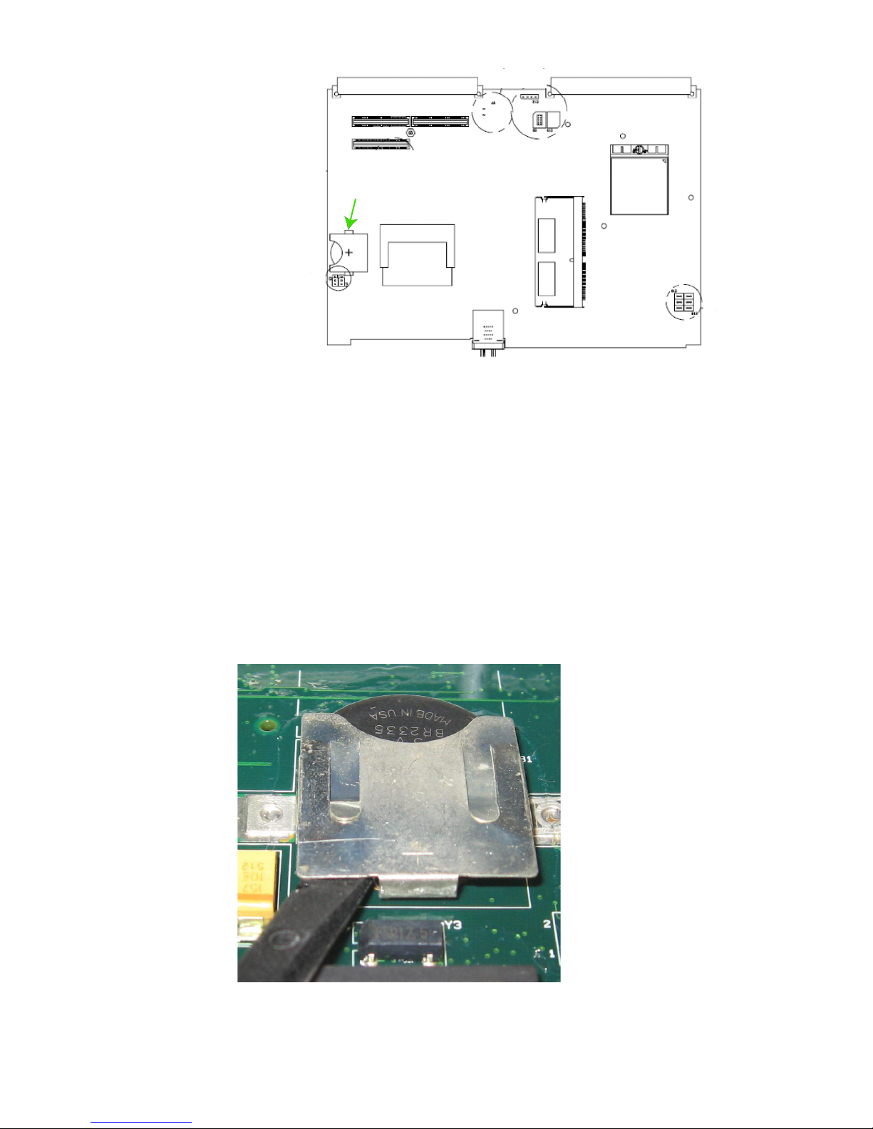
Figure 1-5 Battery Location, Top of Assembly
Battery
1.8 Battery Mounted in Horizontal Holder on the Board
For Battery Removal:
1. Locate the battery on the computer. You may need to reference the Product
Manual if it is not easily located. See Figure 1-5 above.
2. Once the battery is located, take a non-conductive tool and gently push on
the edges of the battery to push it from the socket.
For Battery Installation:
1. Observe correct polarity.
2. Slide the new battery into the socket.
Figure 1-6 Battery Removal
24 VMIVME-7805/VME-7805RC Hardware Reference Manual
Page 25

2 • Standard Features
The VMIVME-7805/VME-7805RC are Intel Pentium 4 Processor - M-based SBCs
compatible with modern industry standard desktop systems. The VMIVME-7805/
VME-7805RC therefore retain industry standard memory and I/O maps along
with standard interrupt architectures. The integrated peripherals described in this
section (such as serial ports, USB port, IDE drives, floppy drives, video controller
and Ethernet controller) are all memory mapped the same as similarly equipped
desktop systems, ensuring compatibility with modern operating systems.
The following sections describe the standard features of the VMIVME-7805/
VME-7805RC.
2.1 CPU
The VMIVME-7805/VME-7805RC CPU sockets are factory populated with a highspeed Pentium 4 Processor - M CPU. The CPU speed and RAM/CompactFlash
size are user specified as part of the VMIVME-7805/VME-7805RC ordering
information.
To change CPU speeds, RAM size or CompactFlash size contact customer care to
receive a Return Material Authorization (RMA).
GE Customer Care is available at: 1-800-433-2682 in North America,
or +1-780-401-7700 for international calls. Or, visit our website www.ge-ip.com.
Standard Features 25
Page 26

2.2 Physical Memory
The VMIVME-7805/VME-7805RC provide DDR Synchronous DRAM (SDRAM)
as onboard system memory. Memory can be accessed as bytes, words or
longwords.
The VMIVME-7805/VME-7805RC accept one PC1600 DDR SDRAM SODIMM for
a maximum capacity of 1 GByte. The onboard SDRAM is dual-ported to the VME
through the PCI-to-VME bridge and is addressable by the local processor, as well
as the VME slave interface by another VME master. Caution must be used when
sharing memory between the local processor and the VME to prevent a VME
master from overwriting the local processor’s operating system.
NOTE
When using the Configure utility of GE IOWorks Access to configure RAM, do not request more than
25 percent of the physical RAM. Exceeding the 25 percent limit may result in known bugs that
causes unpredictable behavior during the boot sequence and requires the use of an emergency
repair disk to restore the computer. It is recommended that an emergency repair disk be kept upto-date and easily accessible.
The VMIVME-7805/VME-7805RC include 32 KByte of nonvolatile SRAM which
can be accessed by the CPU at any time and is used to store system data that must
not be lost during power-off conditions.
NOTE
Memory capacity may be extended as parts become available.
26 VMIVME-7805/VME-7805RC Hardware Reference Manual
Page 27

2.3 Memory and Port Maps
2.3.1 Memory Map - Tundra Universe II-Based PCI-to-VME Bridge
The memory map for the Tundra Universe II-based interface VMIVME-7805/
VME-7805RC is shown in Table 2-1. All systems share this same memory map,
although a VMIVME-7805/VME-7805RC with less than the full 256 MByte of
SDRAM does not fill the entire space reserved for onboard Extended Memory.
Table 2-1 VMIVME-7805/VME-7805RC, Universe II-Based Interface Memory Address Map
MODE MEMORY ADDRESS RANGE SIZE DESCRIPTION
$FFFF 0000 - $FFFF FFFF 64 KByte ROM BIOS Image
$0400 0000 - $FFFE FFFF 3.9 GByte Unused *
$0010 0000 - $0FFF FFFF 255 MByte Reserved for **
PROTECTED MODE
$E0000 - $FFFFF 128 KByte
$D8018 - $DFFFF 32 KByte
$D8016 - $D8017 2 bytes
$D8014 - $D8015 2 bytes
$D8010 - $D8013 2 bytes
$D800E - $D800F 2 bytes
$D8000 - $D800D 14 bytes
$C8000 - $D7FFF 64 KByte
$C0000 - $C7FFF 32 KByte
$A0000 - $BFFFF 128 KByte
REAL MODE
* This space can be used to set up protected mode PCI-to-VME windows (also referred to as PCI slave images).
BIOS will also map onboard PCI based NVRAM, Timers and Watchdog Timers in this area.
$00000 - $9FFFF 640 KByte
Onboard Extended Memory
(not filled on all systems)
Reserved for BIOS Area
2.4 I/O Port Map
** This space can be allocated as shared memory (for example, between the Pentium processor-based CPU and
VME Master). Note that if a PMC board is loaded, the expansion BIOS may be placed in this area.
Like a desktop system, the VMIVME-7805/VME-7805RC include special input/
output instructions that access I/O peripherals residing in I/O addressing space
(separate and distinct from memory addressing space). Locations in I/O address
space are referred to as ports. When the CPU decodes and executes an I/O
instruction, it produces a 16-bit I/O address on lines A00 to A15 and identifies the
I/O cycle with the M/I/O control line. Thus, the CPU includes an independent
64 KByte I/O address space, which is accessible as bytes, words or longwords.
Standard hardware circuitry reserves only 1,024 byte of I/O addressing space
from I/O $000 to $3FF for peripherals. All standard PC I/O peripherals, such as
serial and parallel ports, hard and floppy drive controllers, video system, realtime clock, system timers and interrupt controllers are addressed in this region of
I/O space. The BIOS initializes and configures all these registers properly;
adjusting these I/O ports directly is not normally necessary.
The assigned and user-available I/O addresses are summarized in the I/O Address
Map, Table 2-2.
Standard Features 27
Page 28

Table 2-2 VMIVME-7805/VME-7805RC I/O Address Map
I/O Address Range Size In Bytes HW Device PC/AT Function
$000 - $00F 16 DMA Controller 1
$010 - $01F 16 Reserved
$020 - $021 2 Master Interrupt Controller
$022 - $03F 30 Reserved
$040 - $043 4 Programmable Timer
$044 - $05F 30 Reserved
$060 - $064 5 Keyboard, Speaker, System Configuration
$065 - $06F 11 Reserved
$070 - $071 2 Real-Time Clock
$072 - $07F 14 Reserved
$080 - $08F 16 DMA Page Registers
$090 - $091 2 Reserved
$092 1 Alt. Gate A20/Fast Reset Register
$093 - $09F 11 Reserved
$0A0 - $0A1 2 Slave Interrupt Controller
$0A2 - $0BF 30 Reserved
$0C0 - $0DF 32 DMA Controller 2
$0E0 - $16F 142 Reserved
$170 - $177 8 ICH4-M Secondary Hard Disk Controller
$178 - $1EF 120 User I/O
$1F0 - $1F7 8 ICH4-M Primary Hard Disk Controller
$1F8 - $277 128 User I/O
$278 - $27F 8 I/O Chip Reserved
$280 - $2E7 104 Reserved
$2E8 - $2EE 7 UART* COM4 Serial I/O*
$2EF - $2F7 9 User I/O
$2F8 - $2FE 7 Super-I/O Chip COM2 Serial I/O (16550 Compatible)
$2FF - $36F 113 Reserved
$370 - $377 8 Super-I/O Chip Secondary Floppy Disk Controller
$378 - $37F 8 Super-I/O Chip Reserved
$380 - $3E7 108 Reserved
$3E8 - $3EE 7 UART* COM3 Serial I/O*
$3F0 - $3F7 8 Super-I/O Chip Primary Floppy Disk Controller
$3F8 - $3FE 7 Super-I/O Chip COM1 Serial I/O (16550 Compatible)
$3FF - $4FF 256 Reserved
$500 - CFF 2048 Reserved
* While these I/O ports are reserved for the listed functions, they are not implemented on the VMIVME-7805/
VME-7805RC. They are listed here to make the user aware of the standard PC usage of these ports.
28 VMIVME-7805/VME-7805RC Hardware Reference Manual
Page 29

2.5 Interrupts
2.5.1 System Interrupts
In addition to an I/O port address, an I/O device has a separate hardware
interrupt line assignment. Assigned to each interrupt line is a corresponding
interrupt vector in the 256-vector interrupt table at $00000 to $003FF in memory.
The 16 maskable interrupts and the single Non-Maskable Interrupt (NMI) are
listed in Table 2-3 along with their functions. Table 2-4 on page 30 details the
vectors in the interrupt vector table. The interrupt number in HEX and decimal
are also defined for real and protected mode in Table 2-4 on page 30.
The interrupt hardware implementation on the VMIVME-7805/VME-7805RC is
standard for computers built around the PC architecture, which evolved from the
IBM PC/XT. In the IBM PC/XT computers, only eight interrupt request lines exist,
numbered from IRQ0 to IRQ7 at the PIC. The IBM PC/AT computer added eight
more IRQx lines, numbered IRQ8 to IRQ15, by cascading a second slave PIC into
the original master PIC. IRQ2 at the master PIC was committed as the cascade
input from the slave PIC. This architecture is represented in Figure 2-1 on page 33.
To maintain backward compatibility with PC/XT systems, IBM chose to use the
new IRQ9 input on the slave PIC to operate as the old IRQ2 interrupt line on the
PC/XT Expansion Bus. Thus, in AT systems, the IRQ9 interrupt line connects to
the old IRQ2 pin (pin B4) on the AT Expansion Bus (or ISA bus).
Table 2-3 Interrupt Line Assignments
IRQ AT FUNCTION COMMENTS
NMI Parity Errors (Must be enabled in BIOS Setup) Used by VMIVME-7805/VME-7805RC
0 System Timer Set by BIOS Setup
1 Keyboard Set by BIOS Setup
2Duplexed to IRQ9
3COM2
4COM1
5 Not Assigned
6 Floppy Controller
7 Not Assigned
8Real-Time Clock
9 Old IRQ2 SVGA or Network I/O
10 Not Assigned Determined by BIOS
11 Not Assigned Determined by BIOS
12 Mouse
13 Math Coprocessor
14 AT Hard Drive
15 CompactFlash Drive
PCIbus Interface
Standard Features 29
Page 30

Table 2-4 Interrupt Vector Table
INTERRUPT NO.
HEX DEC
00 0 Divide Error Same as Real Mode
01 1 Debug Single Step Same as Real Mode
02 2 NMI Memory Parity Error,
03 3 Debug Breakpoint Same as Real Mode
04 4 ALU Overflow Same as Real Mode
05 5 Print Screen Array Bounds Check
06 6 Invalid OpCode
07 7 Device Not Available
08 8 IRQ0 Timer T ick Double Exception Detected
09 9 IRQ1 Keyboard Input Coprocessor Segment Overrun
0A 10 IRQ2 BIOS Reserved Invalid Task State Segment
0B 11 IRQ3 COM2 Serial I/O Segment Not Present
0C 12 IRQ4 COM1 Serial I/O Stack Segment Overrun
0D 13 IRQ5 Unassigned Unassigned
0E 14 IRQ6 Floppy Disk Controller Page Fault
0F 15 IRQ7 Unassigned Unassigned
10 16 BIOS Video I/O Coprocessor Error
11 17 System Configuration Check Same as Real Mode
12 18 Memory Size Check Same as Real Mode
13 19 XT Floppy/Hard Drive Same as Real Mode
14 20 BIOS Comm I/O Same as Real Mode
15 21 BIOS Cassette Tape I/O Same as Real Mode
16 22 BIOS Keyboard I/O Same as Real Mode
17 23 BIOS Printer I/O Same as Real Mode
18 24 ROM BASIC Entry Point Same as Real Mode
19 25 Bootstrap Loader Same as Real Mode
1A 26 Time of Day Same as Real Mode
1B 27 Control/Break Handler Same as Real Mode
1C 28 Timer Control Same as Real Mode
1D 29 Video Parameter Table Pntr Same as Real Mode
1E 30 Floppy Parm Table Pntr Same as Real Mode
1F 31 Video Graphics Table Pntr Same as Real Mode
20 32 DOS Terminate Program Same as Real Mode
21 33 DOS Function Entry Point Same as Real Mode
22 34 DOS Terminate Handler Same as Real Mode
23 35 DOS Control/Break Handler Same as Real Mode
24 36 DOS Critical Error Handler Same as Real Mode
25 37 DOS Absolute Disk Read Same as Real Mode
26 38 DOS Absolute Disk Write Same as Real Mode
27 39 DOS Program Terminate,
28 40 DOS Keyboard Idle Loop Same as Real Mode
29 41 DOS CON Dev. Raw Output Same as Real Mode
IRQ
LINE
REAL MODE PROTECTED MODE
Same as Real Mode
VME Interrupts
Stay Resident
(Must be enabled in BIOS Setup)
Same as Real Mode
30 VMIVME-7805/VME-7805RC Hardware Reference Manual
Page 31

Table 2-4 Interrupt Vector Table (Continued)
INTERRUPT NO.
HEX DEC
2A 42 DOS 3.x+ Network Comm Same as Real Mode
2B 43 DOS Internal Use Same as Real Mode
2C 44 DOS Internal Use Same as Real Mode
2D 45 DOS Internal Use Same as Real Mode
2E 46 DOS Internal Use Same as Real Mode
2F 47 DOS Print Spooler Driver Same as Real Mode
30-60 48-96 Reserved by DOS Same as Real Mode
61-66 97-102 User Available Same as Real Mode
67-6F 103-111 Reserved by DOS Same as Real Mode
70 112 IRQ8 Real Time Clock
71 113 IRQ9 Redirect to IRQ2
72 114 IRQ10 Not Assigned
73 115 IRQ11 Not Assigned
74 116 IRQ12 Mouse
75 117 IRQ13 Math Coprocessor
76 118 IRQ14 AT Hard Drive
77 119 IRQ15 CompactFlash Drive
78-7F 120-127 Reserved by DOS Same as Real Mode
80-F0 128-240 Reserved for BASIC Same as Real Mode
F1-FF 241-255 Reserved by DOS Same as Real Mode
IRQ
LINE
REAL MODE PROTECTED MODE
2.5.2 PCI Interrupts
Interrupts on Peripheral Component Interconnect (PCI) Local Bus are optional
and defined as “level sensitive,” asserted low (negative true), using open drain
output drivers. The assertion and de-assertion of an interrupt line, INTx#, is
asynchronous to CLK. A device asserts its INTx# line when requesting attention
from its device driver. Once the INTx# signal is asserted, it remains asserted until
the device driver clears the pending request. When the request is cleared, the
device de-asserts its INTx# signal.
PCI defines one interrupt line for a single function device and up to four interrupt
lines for a multifunction device or connector. For a single function device, only
INTA# may be used while the other three interrupt lines have no meaning.
Figure 2-1 on page 33 depicts the VMIVME-7805/VME-7805RC interrupt logic
pertaining to operations and the PMC site.
Any function on a multifunction device can be connected to any of the INTx#
lines. The Interrupt Pin register defines which INTx# line the function uses to
request an interrupt. If a device implements a single INTx# line, it is called INTA#;
if it implements two lines, they are called INTA# and INTB#; and so forth. For a
multifunction device, all functions may use the same INTx# line, or each may
have its own (up to a maximum of four functions), or any combination thereof. A
single function can never generate an interrupt request on more than one INTx#
line.
The slave PIC accepts the interrupts through lines that are defined by the BIOS.
The BIOS defines which interrupt line to utilize depending on which system
requires the use of the line.
Standard Features 31
Page 32

2.6 PCI Device Interrupt Map
The PCI bus-based external devices include the PMC sites, Ethernet controller
and the PCI-to-VME bridge. The default BIOS maps these external devices to the
PCI Interrupt Request (PIRQx) lines of the ICH2. This mapping is illustrated in
Figure 2-1 on page 33 and is defined in Table 2-5.
The device PCI interrupt lines (INTA through INTH) that are present on each
device cannot be modified.
Table 2-5 PCI Device Interrupt Mapping by the BIOS
Device Component
PCI-to-VME Bridge Tundra Universe IIB 0x10E3 0x0000 AD19 INTA REQ0
Timer/SRAM FPGA GE Proprietary 0x114A 0x0004 AD20 INTE N/A
PMC N/A N/A N/A AD31 INTC REQ2
Ethernet Controller Intel 82540EM*
Intel 82541PI
PCI Host Bridge GMCH 0x8086 0x3580 N/A N/A N/A
Memory Controller GMCH 0x8086 0x3584 N/A N/A N/A
Configuration and
Process
Integrated
Graphics
PCI-LPC Bridge ICH4-M 0x8086 0x24CC N/A N/A N/A
USB VHCI
Controller
SMBus Controller ICH4-M 0x8086 0x24C3 N/A N/A N/A
LAN Controller ICH4-M 0x8086 0x10E3 N/A N/A N/A
USB VHCI
Controller
GMCH 0x8086 0x3585 N/A N/A N/A
GMCH 0x8086 0x3582 N/A N/A N/A
ICH4-M 0x8086 0x24C2 N/A N/A N/A
ICH4-M 0x8086 0x24CD N/A N/A N/A
Vendor
ID
0x8086 0x100E
DeviceIDCPU Address
Map ID Select
AD22 INTB REQ1
0x1076
PCI IRQ
Arbitration
Request Line
PCI-to-Hub Bridge ICH4-M 0x8086 0x2448 N/A N/A N/A
*Intel 82540EM for VMIVME-7805 or Intel 82541PI for VME-7805RC.
32 VMIVME-7805/VME-7805RC Hardware Reference Manual
Page 33

Figure 2-1 Connections for the PC Interrupt Logic Controller
INTR
Keybd
Timer
INT
IRQ0 IRQ1
Real-Tm
Clock
Ethernet
Cltr
IRQ8 IRQ9
Cltr/Sbus USB
IRQ10
I/O Controller Hub
ICH4-M
INTA
PMC
Site
INTB
INTC
INTD
CPU
82540 MASTER-
Interrupt
8-15
Com 2
IRQ2 IRQ4 IRQ5
Video,Ethernet
CONNECTIONS
MAPPED BY BIOS
PCI INTERRUPT
PIRQA PIRQB PIRQC PIRQD
82540 SLAVE-
Mouse Math
IRQ12IRQ11 IRQ13
MAPPER
Com 1
Coproc
PORTS $020-$021
Floppy
Unused
Control
IRQ6IRQ3
PORTS $0A0-$0A1
AT
Hard Drv
IRQ14
PIRQE
Flash
Drive
IRQ15
Unused
IRQ7
V
M
E
Universe IIB
PCI-to-VME
Bus
BRIDGE
INT
82540EM
Ethernet
Timers/SRAM
INT
FPGA
The PCI-to-VME Bridge has the capability of generating an NMI via the PCI
SERR# line. Table 2-6 describes the register bits that are used by the NMI. The
SERR interrupt is routed through logic back to the NMI input line on the CPU.
The CPU reads the NMI Status Control register to determine the NMI source (bits
set to 1). After the NMI interrupt routine processes the interrupt, software clears
the NMI status bits by setting the corresponding enable/disable bit to 1. The NMI
Enable and Real-Time Clock register can mask the NMI signal and disable/enable
all NMI sources.
Standard Features 33
Page 34

Table 2-6 NMI Register Bit Descriptions
Status Control Register (I/O Address $061, Read/Write, Read Only)
Bit 7 SERR# NMI Source Status (Read Only) - This bit is set to 1 if a system board agent detects a
Bit 2 PCI SERR# Enable (Read/Write) - 1 = Clear and Disable, 0 = Enable
Enable and Real-Time Clock Address Register (I/O Address $070, Write Only)
Bit 7 NMI Enable - 1 = Disable, 0 = Enable
system board error. It then asserts the PCI SERR# line. To reset the interrupt, set Bit 2 to 0 and
then set it to 1. When writing to port $061, Bit 7 must be 0.
2.7 Integrated Peripherals
The VMIVME-7805/VME-7805RC incorporate a National Semiconductor
Super I/O (SIO) chip. The SIO provides the VMIVME-7805/VME-7805RC with a
standard floppy drive controller, two 16550 UART-compatible serial ports,
keyboard and mouse ports and general purpose I/O for system monitoring
functions. Both serial port signals are available from the front panel. The floppy
signals are available via the VME backplane connectors and can be accessed with
the appropriate RTM (VMIACC-0562/ACC-0562RC).
The IDE interface is provided by the Intel I/O Controller Hub (ICH4-M) chip. The
IDE interface supports two channels known as the primary and secondary
channels. The secondary channel is routed onboard to the optional CompactFlash
socket. The primary channel is routed out the VME backplane and can be
accessed using a VMIACC-0562/ACC-0562RC RTM which terminates into a
standard 40-pin header. This channel can support two drives, a master and slave.
The IDE interface on the VMIVME-7805/VME-7805RC supports Ultra ATA/33,
Ultra ATA/66 and Ultra ATA/100 drives and automatically determines the proper
operating mode based on the type of drive used. In order to properly function in
the Ultra ATA/100 mode, a special 80 conductor cable must be used instead of the
standard 40 conductor cable. This cable is typically available from the
Ultra ATA/100 drive manufacturer.
34 VMIVME-7805/VME-7805RC Hardware Reference Manual
Page 35

2.8 Ethernet Controller
The VMIVME-7805/VME-7805RC support Ethernet LANs with two Intel Ethernet
controllers (one 82540EM GbE controller for the VMIVME-7805 or one 82541PI for
the VME-7805RC and the other 10Base-T, 100Base-TX). GbE options are
supported via the front panel RJ45 connectors; 10Base-T and 100Base-TX is
supported via a second RJ45 connector.
10Base-T A network based on the 10Base-T standard uses unshielded twisted-pair cables,
providing an economical solution to networking by allowing the use of existing
telephone wiring and connectors. The RJ45 connector is used with the 10Base-T
standard. 10Base-T has a maximum length of 100 meters.
100Base-TX The VMIVME-7805/VME-7805RC also support the 100Base-TX Ethernet.
A network based on a 100Base-TX standard uses unshielded twisted-pair cables
and a RJ45 connector. 100Base-TX has a maximum length of 100 meters.
1000Base-T The VMIVME-7805/VME-7805RC support GbE offering speeds of 1000Mb/s. It is
fully compatible with existing Ethernets, as it uses the same CSMA/CD and MAC
protocols. 1000BaseT has a maximum length of 3000 meters using Single-mode
Fiber-Optic cables.
Boot ROM BIOS The VMIVME-7805/VME-7805RC support booting on the 10/100 Mbit Ethernet
port using a ROM Ethernet BIOS. Refer to Appendix D: Argon BIOS, page 76 for
more information on remote Ethernet booting.
Standard Features 35
Page 36

2.9 Video Graphics Adapter
High-resolution graphics and multimedia-quality video are supported on the
VMIVME-7805/VME-7805RC using the 852GM (GMCH) chipset internal graphics
controller. Screen resolutions up to 1,600 x 1,200 x 256 colors (single view mode)
are supported by the graphics adapter.
Table 2-7 Partial List of Display Modes Supported
Resolution
320 x 200 70 70 70
320 x 240 70 70 70
352 x 480 70 70 70
352 x 576 70 70 70
400 x 300 70 70 70
512 x 384 70 70 70
640 x 400 70 70 70
640 x 480 60, 70, 72, 75, 85 60, 70, 72, 75, 85 60, 70, 72, 75, 85
720 x 480 75, 85 75, 85 75, 85
720 x 576 60, 75, 85 60, 75, 85 60, 75, 85
800 x 600 60, 70, 72, 75, 85 60, 70, 72, 75, 85 60, 70, 72, 75, 85
1,024 x 768 60, 70, 72, 75, 85 60, 70, 72, 75, 85 60, 70, 72, 75, 85
1,152 x 864 60, 70, 72, 75, 85 60, 70, 72, 75, 85 60, 70, 72, 75, 85
1,280 x 720 60, 75, 85 60, 75, 85 60, 75, 85
1,280 x 960 60, 75, 85 60, 75, 85 60, 75, 85
1,280 x 1,024 60, 70, 72, 75, 85 60, 70, 72, 75, 85 60, 70, 75, 85
1,600 x 900 60, 75, 85 60, 75, 85
1,600 x 1,200 60, 70, 72, 75
Bits Per Pixel (Frequency in Hz)
8-bit Indexed 16-bit 24-bit
NOTE
Not all SVGA monitors support resolutions and refresh rates beyond 640 x 480 at 85 Hz. Do not
attempt to drive a monitor to a resolution or refresh rate beyond its capability.
36 VMIVME-7805/VME-7805RC Hardware Reference Manual
Page 37

2.9.1 Digital Video Interface (DVI)
The VMIVME-7805/VME-7805RC have a Digital Visual Interface that provides a
high-speed digital connection for visual data types that are display technology
independent. DVI is a display interface developed in response to the proliferation
of digital flat panel displays. For the most part, these displays are currently
connected to an analog Video Graphics Array (VGA) interface and, thus, require a
double conversion.
The digital signal from the computer must be converted to an analog signal for
the analog VGA interface, then converted back to a digital signal for processing
by the flat panel display. This inherently inefficient process takes a toll on
performance and video quality and adds cost. In contrast, when a flat panel
display is connected to a digital interface, no digital-to-analog conversion is
required.
DVI uses Silicon Image's PanelLink, a high-speed serial interface that uses
Transition Minimized Differential Signaling (TMDS) to send data to the monitor.
The DFP and VESA Plug and Display interfaces also use PanelLink. For this
reason, DVI can work with these previous interfaces by using adapter cables
(depending on the signal quality of the adapter.)
DVI also supports the VESA Display Data Channel (DDC) and the Extended
Display Identification Data (EDID) specifications. DDC is a standard
communications channel between the display adapter and monitor. EDID is a
standard data format containing monitor information such as vendor
information, monitor timing, maximum image size, and color characteristics.
EDID information is stored in the display and is communicated over the DDC.
EDID and DDC enable the system, display and graphics adapter to communicate
so that the system can be configured to support specific features available in the
display.
2.9.2 DVI Connectors
The DVI connector has 24 pins that can accommodate up to two TMDS links and
the VESA DDC and EDID services. The DVI specification defines two types of
connectors (see Figure 1):
• DVI-Digital (DVI-D) supports digital displays only (not supported)
• DVI-Integrated (DVI-I) supports digital displays and is backward compatible with analog displays (used on the VMIVME-7805/VME-7805RC)
The VMIVME-7805/VME-7805RC use the DVI-I connector with a single TMDS
link. The DVI-I interface accommodates a 12- or 24-pin DVI plug connector or a
new type of analog plug connector that uses four additional pins, plus a ground
plane plug to maintain a constant impedance for the analog RGB signals. The
DVI-I adapter is supplied by GE.
Standard Features 37
Page 38

2.10 Universal Serial Bus
The VMIVME-7805/VME-7805RC provide a single USB connection on the front
panel. The onboard USB controller supports the standard USB interface Rev. 2.0.
The USB Host Controller moves data between system memory and the USB by
processing and scheduling data structures. The controller executes the scheduled
lists, and reports status back to the system.
38 VMIVME-7805/VME-7805RC Hardware Reference Manual
Page 39

3 • Embedded PC/RTOS Features
GE VMIVME-7805/VME-7805RC feature additional capabilities beyond those of a
typical desktop computer system. The unit provides four software-controlled,
general-purpose timers along with a programmable Watchdog Timer for
synchronizing and controlling multiple events in embedded applications. The
VMIVME-7805/VME-7805RC also provide a CompactFlash system and 32 KByte
of nonvolatile SRAM. Also, the
VMIVME-7805/VME-7805RC support an embedded intelligent VME bridge to
allow compatibility with the most demanding VME applications. These features
make the unit ideal for embedded applications, particularly where standard hard
drives and floppy disk drives cannot be used. The VMIVME-7805/VME-7805RC
also support I
3.1 VME Bridge
In addition to their PC/AT functions, the VMIVME-7805/VME-7805RC have the
following VME features:
• Complete six-line Address Modifier (AM-Code) programmability
• VME data interface with separate hardware byte/word swapping for master
and slave accesses
2
C by integrating specialized circuitry for these functions.
• Support for VME64 multiplexed MBLT 64-bit VME block transfers
• User-configured interrupter
• User-configured interrupt handler
• System Controller mode with programmable VME arbiter (PRI, SGL and
RRS modes are supported)
• VME BERR bus error timer (software programmable)
• Slave access from the VME to local RAM and mailbox registers
• Full-featured programmable VME requester (ROR, RWD and BCAP modes
are supported)
• System Controller auto detection
• Complete VME master access through five separate Protected-mode memory windows
The VMIVME-7805/VME-7805RC support High Throughput DMA transfers of
bytes, words and longwords in both Master and Slave configurations.
If Endian conversion is not needed, GE offers a special “Bypass” mode that can be
used to further enhance throughput (not available for byte transfers).
The VMIVME-7805/VME-7805RC VME interface is provided by the PCI-to-VME
bridge built around the Tundra Semiconductor Corporation Universe II VME
interface chip. The Universe II provides a reliable high-performance 64-bit VMEto-PCI interface in one design. The functions and programming of the Universebased VME interface are addressed in detail in a companion manual titled:
GE Intelligent Platforms’ Tundra Universe II Based VME Interface Product Manual
(500-000211-000).
Embedded PC/RTOS Features 39
Page 40

3.2 I2C Support
The VMIVME-7805/VME-7805RC support the I2Cbus and can operate as an
2
Cbus master or slave per the I2Cbus specification, version 2.0, developed by
I
Philips Semiconductor. Communication over the I
the use of the National Semiconductor Super I/O I
2
is capable of communicating on the I
Cbus on a byte-wise basis using interrupt or
2
Cbus is accomplished through
2
Cbus controller. This controller
polled handshaking and supports a programmable clock rate when operating in
Master mode. The I
2
Cbus signals are available through the VMIVME-7805/
VME-7805RC E12 header as shown in Table 3-1.
Table 3-1 I2Cbus Through E12
Signal Name Pin
+5.0 V 1
I2C_SDA 2
I2C_SCL 3
GND 4
The VMIVME-7805/VME-7805RC provide termination on the I
2
C signals.
The controller can issue interrupts to the VMIVME-7805/VME-7805RC when
2
handshaking on the I
Cbus. When the I2Cbus controller drives the interrupt
active, software must service and then clear the interrupt. Software can determine
the cause of the interrupt by reading the bit of the status register.
2
For more information related to programming the I
Cbus controller, see the
section “Access, Bus Interface (ACB)” in the “PC87366 128-pin LPC Super I/O with
System Hardware Monitoring and MIDI and Game Ports” datasheet available from
National Semiconductor.
40 VMIVME-7805/VME-7805RC Hardware Reference Manual
Page 41

3.3 Embedded PCI Functions
The VMIVME-7805/VME-7805RC provide nonvolatile RAM (NVRAM), Timers
and a Watchdog Timer via the PCI bus. These functions are required for
embedded and real time applications. The PCI configuration space of these
embedded functions are shown below.
Table 3-2 PCI Configuration Space Registers
31 16 15 00
Device ID 0004 Vendor ID 114A 00h
Status Command 04h
Class Code Revision ID 08h
BIST Header Type Latency Timer Cache Line Size 0Ch
PCI Base Address 0 for Memory-Mapped VME Control registers (BAR0) 10h
PCI Base Address 1 for Memory-Mapped 32 KByte NVRAM (BAR1) 14h
PCI Base Address 2 for memory-mapped Watchdog and other timers (BAR2)
Reserved
Reserved
Reserved
Reserved
Subsystem ID 7805 Subsystem Vendor ID 114A
Reserved
Reserved
Reserved
Max_Lat Min_gnt Interrupt Pin Interrupt Line 3Ch
Register
Address
18h
1Ch
20h
24h
28h
2Ch
30h
34h
38h
The “Device ID” field indicates that the device is for VME products (00) and
indicates the supported embedded feature set.
The “Vendor ID” and “Subsystem Vendor ID” fields indicate GE PICMG
®
assigned Vendor ID (114A).
The “Subsystem ID” field indicates the model number of the product (7805).
Embedded PC/RTOS Features 41
Page 42

3.4 Timers
3.4.1 General
The VMIVME-7805/VME-7805RC provide four user-programmable timers (two
16-bit and two 32-bit) which are completely dedicated to user applications and are
not required for any standard system function. Each timer is clocked by
independent generators with selectable rates of 2 MHz, 1 MHz, 500 kHz and
250 kHz. Each timer may be independently enabled and each is capable of
generating a system interrupt on timeout.
Events can be timed by either polling the timers or enabling the interrupt
capability of the timer. A status register allows for application software to
determine which timer is the cause of any interrupt.
3.4.2 Timer Control Status Register 1 (TCSR1)
The timers are controlled and monitored via the Timer Control Status Register 1
(TCSR1) located at offset 0x00 from the address in BAR2. The mapping of the bits
in this register are as follows:
Field Bits Read or Write
Timer 1 Caused IRQ TCSR1[0] R/W
Timer 1 Enable TCSR1[1] R/W
Timer 1 IRQ Enable TCSR1[2] R/W
Timer 1 Clock Select TCSR1[4..3] R/W
Timer 2 Caused IRQ TCSR1[8] R/W
Timer 2 Enable TCSR1[9] R/W
Timer 2 IRQ Enable TCSR1[10] R/W
Timer 2 Clock Select TCSR1[12..11] R/W
Timer 3 Caused IRQ TCSR1[16] R/W
Timer 3 Enable TCSR1[17] R/W
Timer 3 IRQ Enable TCSR1[18] R/W
Timer 3 Clock Select TCSR1[20..19] R/W
Timer 4 Caused IRQ TCSR1[24] R/W
Timer 4 Enable TCSR1[25] R/W
Timer 4 IRQ Enable TCSR1[26] R/W
Timer 4 Clock Select TCSR1[28..27] R/W
Reserved All Other Bits R/W
All of these bits default to “0” after system reset.
Each timer has an independently selectable clock source which is selected by the
bit pattern in the “Timer x Clock Select” field as follows:
Clock Rate MSb LSb
2MHz 0 0
1MHz 0 1
500kHz 1 0
250kHz 1 1
Each timer can be independently enabled by writing a “1” to the appropriate
“Timer x Enable” field. Similarly, the generation of interrupts by each timer can
42 VMIVME-7805/VME-7805RC Hardware Reference Manual
Page 43

be independently enabled by writing a “1” to the appropriate “Timer x IRQ
Enable” field.
If an interrupt is generated by a timer, the source of the interrupt may be
determined by reading the “Timer x Caused IRQ” fields. If the field is set to “1”,
then the respective timer caused the interrupt. Note that multiple timers can
cause a single interrupt. Therefore, the status of all timers must be read to ensure
that all interrupt sources are recognized.
A particular timer interrupt can be cleared by writing a “0” to the appropriate
“Timer x Caused IRQ” field. Alternately, a write to the appropriate Timer x IRQ
Clear (TxIC) register will also clear the interrupt. When clearing the interrupt
using the “Timer x Caused IRQ” fields, note that it is very important to ensure
that a proper bit mask is used so that other register settings are not affected. The
preferred method for clearing interrupts is to use the “ Timer 1 IRQ Clear (T1IC)”
registers described on page 44.
3.4.3 Timer Control Status Register 2 (TCSR2)
The timers are also controlled by bits in the Timer Control Status Register 2
(TCSR2) located at offset 0x04 from the address in BAR2. The mapping of the bits
in this register are as follows:
Field Bits Read or Write
Read Latch Select TCSR2[0] Read/Write
Reserved All Other Bits Read/Write
All of these bits default to “0” after system reset.
The “Read Latch Select” bit is used to select the latching mode of the
programmable timers. If this bit is set to “0”, then each timer output is latched
upon a read of any one of its addresses. For example, a read to the TMRCCR12
register latches the count of timers 1 and 2. A read to the TMRCCR3 register
latches the count of timer 3. This continues for every read to any one of these
registers. As a result, it is not possible to capture the values of all four timers at a
given instance in time. However, by setting this bit to “1”, all four timer outputs
will be latched only on reads to the Timer 1 & 2 Current Count Register
(TMRCCR12). Therefore, to capture the current count of all four timers at the
same time, perform a read to the TMRCCR12 first (with a 32-bit read), followed
by a read to TMRCCR3 and TMRCCR4. The first read (to the TMRCCR12 register)
causes all four timer values to be latched at the same time. The subsequent reads
to the TMRCCR3 and TMRCCR4 registers do not latch new count values,
allowing the count of all timers at the same instance in time to be obtained.
3.4.4 Timer 1 & 2 Load Count Register (TMRLCR12)
Timers 1 & 2 are 16-bits wide and obtain their load count from the Timer 1 & 2
Load Count Register (TMRLCR12), located at offset 0x10 from the address in
BAR2. The mapping of bits in this register are as follows:
Field Bits Read or Write
Timer 2 Load Count TMRLCR12[31..16] Read/Write
Timer 1 Load Count TMRLCR12[15..0] Read/Write
When either of these fields are written (either by a single 32-bit write or separate
16-bit writes), the respective timer is loaded with the written value on the next
rising edge of the timer clock, regardless of whether the timer is enabled or
Embedded PC/RTOS Features 43
Page 44

disabled. The value stored in this register is also automatically reloaded on
terminal count (or timeout) of the timer.
3.4.5 Timer 3 Load Count Register (TMRLCR3)
Timer 3 is 32-bits wide and obtains its load count from the Timer 3 Load Count
Register (TMRLCR3), located at offset 0x14 from the address in BAR2. The
mapping of bits in this register are as follows:
Field Bits Read or Write
Timer 3 Load Count TMRLCR3[31..0] Read/Write
When this field is written, Timer 3 is loaded with the written value on the next
rising edge of the timer clock, regardless of whether the timer is enabled or
disabled. The value stored in this register is also automatically reloaded on
terminal count (or timeout) of the timer.
3.4.6 Timer 4 Load Count Register (TMRLCR4)
Timer 4 is 32-bits wide and obtains its load count from the Timer 4 Load Count
Register (TMRLCR4), located at offset 0x18 from the address in BAR2. The
mapping of bits in this register are as follows:
Field Bits Read or Write
Timer 4 Load Count TMRLCR4[31..0] Read/Write
When this field is written, Timer 4 is loaded with the written value on the next
rising edge of the timer clock, regardless of whether the timer is enabled or
disabled. The value stored in this register is also automatically reloaded on
terminal count (or timeout) of the timer.
3.4.7 Timer 1 & 2 Current Count Register (TMRCCR12)
The current count of timers 1 & 2 may be read via the Timer 1 & 2 Current Count
Register (TMRCCR12), located at offset 0x20 from the address in BAR2. The
mapping of bits in this register are as follows:
Field Bits Read or Write
Timer 2 Count TMRCCR12[31..16] Read Only
Timer 1 Count TMRCCR12[15..0] Read Only
When either field is read, the current count value is latched and returned. There
are two modes that determine how the count is latched depending on the setting
of the “Read Latch Select” bit in the WDT Control Status Register (CSR2). See the
CSR2 register description for more information on these two modes.
3.4.8 Timer 3 Current Count Register (TMRCCR3)
The current count of Timer 3 may be read via the Timer 3 Current Count Register
(TMRCCR3), located at offset 0x24 from the address in BAR2. The mapping of bits
in this register are as follows:
Field Bits Read or Write
Timer 3 Count TMRCCR3[31..0] Read Only
When this field is read, the current count value is latched and returned. There are
two modes that determine how the count is latched depending on the setting of
44 VMIVME-7805/VME-7805RC Hardware Reference Manual
Page 45

the “Read Latch Select” bit in the WDT Control Status Register (CSR2). See the
CSR2 register description for more information on these two modes.
3.4.9 Timer 4 Current Count Register (TMRCCR4)
The current count of Timer 4 may be read via the Timer 4 Current Count Register
(TMRCCR4), located at offset 0x28 from the address in BAR2. The mapping of bits
in this register are as follows:
Field Bits Read or Write
Timer 4 Count TMRCCR4[31..0] Read Only
When this field is read, the current count value is latched and returned. There are
two modes that determine how the count is latched depending on the setting of
the “Read Latch Select” bit in the WDT Control Status Register (CSR2). See the
CSR2 register description for more information on these two modes.
3.4.10 Timer 1 IRQ Clear (T1IC)
The Timer 1 IRQ Clear (T1IC) register is used to clear an interrupt caused by
Timer 1. Writing to this register, located at offset 0x30 from the address in BAR2,
causes the interrupt from Timer 1 to be cleared. This can also be done by writing a
“0” to the appropriate “Timer x Caused IRQ” field of the timer Control Status
Register (CSR1). This register is write only and the data written is irrelevant.
3.4.11 Timer 2 IRQ Clear (T2IC)
The Timer 2 IRQ Clear (T2IC) register is used to clear an interrupt caused by
Timer 2. Writing to this register, located at offset 0x34 from the address in BAR2,
causes the interrupt from Timer 2 to be cleared. This can also be done by writing a
“0” to the appropriate “Timer x Caused IRQ” field of the timer Control Status
Register (CSR1). This register is write only and the data written is irrelevant.
3.4.12 Timer 3 IRQ Clear (T3IC)
The Timer 3 IRQ Clear (T3IC) register is used to clear an interrupt caused by
Timer 3. Writing to this register, located at offset 0x38 from the address in BAR2,
causes the interrupt from Timer 3 to be cleared. This can also be done by writing a
“0” to the appropriate “Timer x Caused IRQ” field of the timer Control Status
Register (CSR1). This register is write only and the data written is irrelevant.
3.4.13 Timer 4 IRQ Clear (T4IC)
The Timer 4 IRQ Clear (T4IC) register is used to clear an interrupt caused by
Timer 4. Writing to this register, located at offset 0x3C from the address in BAR2,
causes the interrupt from Timer 4 to be cleared. This can also be done by writing a
“0” to the appropriate “Timer x Caused IRQ” field of the timer Control Status
Register (CSR1). This register is write only and the data written is irrelevant.
Embedded PC/RTOS Features 45
Page 46

3.5 Watchdog Timer
3.5.1 General
The VMIVME-7805/VME-7805RC provide a programmable Watchdog Timer
(WDT) which can be used to reset the system if software integrity fails.
3.5.2 WDT Control Status Register (WCSR)
The WDT is controlled and monitored by the WDT Control Status Register
(WCSR) which is located at offset 0x08 from the address in BAR2. The mapping of
the bits in this register are as follows:
Field Bits Read or Write
SERR/RST Select WCSR[16] Read/Write
WDT Timeout Select WCSR[10..8] Read/Write
WDT Enable WCSR[0] Read/Write
All of these bits default to “0” after system reset. All other bits are reserved.
The “WDT Timeout Select” field is used to select the timeout value of the
Watchdog Timer as follows:
Timeout WCSR[10] WCSR[9] WCSR[8]
135s 0 0 0
33.6s 001
2.1s 0 1 0
524ms 0 1 1
262ms 1 0 0
131ms 1 0 1
32.768ms 1 1 0
2.048ms 1 1 1
The “SERR/RST Select” bit is used to select whether the WDT generates an SERR#
on the local PCI bus or a system reset. If this bit is set to “0”, the WDT will
generate a system reset. Otherwise, the WDT will make the local PCI bus SERR#
signal active.
The “WDT Enable” bit is used to enable the Watchdog Timer function. This bit
must be set to “1” in order for the Watchdog Timer to function. Note that since all
registers default to zero after reset, the Watchdog Timer is always disabled after a
reset. The Watchdog Timer must be re-enabled by the application software after
reset in order for the Watchdog Timer to continue to operate. Once the Watchdog
Timer is enabled, the application software must refresh the Watchdog Timer
within the selected timeout period to prevent a reset or SERR# from being
generated. The Watchdog Timer is refreshed by performing a write to the WDT
Keepalive register (WKPA). The data written is irrelevant.
3.5.3 WDT Keepalive Register (WKPA)
When enabled, the Watchdog Timer is prevented from resetting the system by
writing to the WKPA located at offset 0x0C from the address in BAR2 within the
selected timeout period. The data written to this location is irrelevant.
46 VMIVME-7805/VME-7805RC Hardware Reference Manual
Page 47

3.6 NVRAM
3.7 VME Control
The VMIVME-7805/VME-7805RC provide 32 KByte of nonvolatile SRAM. This
memory is mapped in 32k of address space starting at the address in BAR1. This
memory is available at any time and supports byte, short word and long word
accesses from the PCI bus. The contents of this memory is retained when the
power to the board is removed.
The following table shows the register definitions for the VMIVME-7805/
VME-7805RC (offset from BAR0).
Table 3-3 Register Definitions Offset From BAR0
Register Name Offset
VMECOMM 0x00
Bit Name Bit Definition
MEC_SEL 0 Master big-endian enable bit 1=Big Endian 0=Little
Endian bit
SEC_SEL 1 Slave Big-Endian enable bit 1=Big Endian 0=Little Endian
ABLE 2 Auxiliary BERR logic enable bit
1=Aux. BERR enabled 0=Aux. BERR disabled
BTO 3 Bus error timer enabled 1=enabled 0=disabled
BTOV [1:0] 5:4 Timeout value
00 - 16 µs
01 - 64 µs
10 -256 µs
11 - 1.00 ms
BERRI 6 BERR interrupt enable 1=Interrupt enabled 0=Interrupt
disabled
BERRST 7 BERR status read/clear bit
1=Clear BERR status 0=Do nothing
SFENA 8 Enables generation of VME SYSFAIL upon WDT timeout
1= Enable SYSFAIL generation 0=Disable
Unused 9 Not Used
BPENA 10 Endian conversion bypass bit
1 = bypass 0 = not bypassed
VBENA 11 VME enable bit
1 = enabled 0 = disabled
Unused 31:12 Not Used
VBAR 0x08
VME_ADDR All Latched VME Address
VBAM 0x04
VME_ADDR 5:0 Latched VME Address Modifier
Unused 31:6 Not Used
SEC_SEL 0x001
Please refer to Table 3-2, PCI Configuration Space Registers, on page 41 for more
information concerning BAR0.
Embedded PC/RTOS Features 47
Page 48

3.8 CompactFlash
The VMIVME-7805/VME-7805RC feature an optional onboard CompactFlash
mass storage system with a capacity of up to 1 GByte. This CompactFlash appears
to the user as an intelligent ATA (IDE) disk drive with the same functionality and
capabilities as a “rotating media” IDE hard drive. The VMIVME-7805/
VME-7805RC BIOS includes an option to allow the board to boot from the
CompactFlash when loaded with user-supplied operating system.
The CompactFlash resides on the VMIVME-7805/VME-7805RC as the secondary
IDE bus master device (the secondary IDE bus slave device is not assignable).
3.9 Remote Ethernet Booting
The VMIVME-7805/VME-7805RC are capable of booting from a server using the
10/100 Mbit Ethernet port over a network utilizing ARGON’s Boot ROM BIOS.
The Boot ROM BIOS gives you the ability to remotely boot the VMIVME-7805/
VME-7805RC using a variety of network protocols. The Ethernet must be
connected through the front panel (RJ45) connector to boot remotely. This feature
allows users to create systems without the worry of disk drive reliability, or the
extra cost of adding CompactFlash Drives.
3.9.1 BootWare Features:
• Netware (802.1, 802.3 or EthII), TCP/IP (DHCP or BootP), RPL and PXE boot
support
• Unparalleled boot sector virus protection
• Detailed boot configuration screens
• Comprehensive diagnostics
• Optional disabling of local boots
• Dual-boot option lets users select network or local booting
48 VMIVME-7805/VME-7805RC Hardware Reference Manual
Page 49

Maintenance
If a GE product malfunctions, please verify the following:
1. Software version resident on the product
2. System configuration
3. Electrical connections
4. Jumper or configuration options
5. Boards are fully inserted into their proper connector location
6. Connector pins are clean and free from contamination
7. No components or adjacent boards were disturbed when inserting or removing the board from the chassis
8. Quality of cables and I/O connections
If products must be returned, contact GE for a Return Material Authorization
(RMA) Number. This RMA Number must be obtained prior to any return from
Customer Care.
GE Customer Care is available at: 1-800-433-2682 in North America,
or +1-780-401-7700 for international calls. Or, visit our website at:
www.ge-ip.com
Maintenance Prints
User level repairs are not recommended. The drawings and diagrams in this
manual are for reference purposes only.
Maintenance 49
Page 50

Compliance Information
This chapter provides the applicable information regarding regulatory
compliance for the VMIVME-7805/VME-7805RC.
GE VMIVME-7805/VME-7805RC have been evaluated to and have met the
requirements for compliance to the following standards:
International Compliance
• EN55022:1998/CISPR 22:1997
• IEC61000-4-2
• IEC61000-4-3
• IEC61000-4-4
• IEC61000-4-5
• IEC61000-4-6
European Union (CE Mark)
• BS EN55024 (1998 w A1:01 & A2: 03)
• BS EN55022 (Class A)
United States
• FCC Part 15, Subpart B, Section 109, Class A
Australia/New Zealand
• AS/NZS CISPR 22 (2002) Class A
Canada
• ICES-003 Class A
50 VMIVME-7805/VME-7805RC Hardware Reference Manual
Page 51

FCC Part 15
This device complies with Part 15 of the FCC Rules. Operation is subject to the
following two conditions: (1) this device may not cause harmful interference, and
(2) this device must accept any interference received, including interference that
may cause undesired operation.
FCC Class A
NOTE
This equipment has been tested and found to comply with the limits for a Class A digital device,
pursuant to Part 15 of the FCC Rules. These limits are designed to provide reasonable protection
against harmful interference when the equipment is operated in a commercial environment. This
equipment generates, uses, and can radiate radio frequency energy and, if not installed and used
in accordance with the instruction manual, may cause harmful interference to radio
communications. Operation of this equipment in a residential area is likely to cause harmful
interference in which case the user will be required to correct the interference at his own expense.
CAUTION
Changes or modifications not expressly approved by the party responsible for
compliance could void the user’s authority to operate the equipment .
Canadian Regulations
The VMIVME-7805/VME-7805RC Class A digital apparatus complies with
Canadian ICES-003.
NOTE
Any equipment tested and found compliant with FCC Part 15 for unintentional radiators or
EN55022 (previously CISPR 22) satisfy ICES-003.
Compliance 51
Page 52

A • Appendix A: Connectors and Pinouts
The VMIVME-7805/VME-7805RC VME SBCs have several connectors for their I/O
ports. Wherever possible, the VMIVME-7805/VME-7805RC use connectors and
pinouts typical for any desktop PC. This ensures maximum compatibility with a
variety of systems.
Connector diagrams in this appendix are generally shown in a natural orientation
with the controller board mounted in a VME chassis.
A.1 VME Connector Pinout (P1 and P2)
Figure A-1 shows the location of the VME P1 and P2 connectors and their
orientation on the VMIVME-7805/VME-7805RC. Table A-1 shows the pin
assignments for the VME connectors. Note that only Row B of connector P2 is
used; all other pins on P2 are reserved and should not be connected.
Figure A-1 VME Connector Diagram
32
P2
Row
32
D
C
B
A
Z
1
P1
1
Table A-1 VME Connector Pinout
P1 Row A
Pin#
Signal
1 D00 BBSY# D08 CONN [2] CBL_DETECT +5V IDE RST# CONN [1]
2 D01 BCLR# D09 GND PDD8 GND PDD7 CONN [3]
3 D02 ACFAIL D10 CONN [5] PDD9 Reserved PDD6 CONN [4]
4 D03 BG0IN# D11 GND PDD10 A24 PDD5 CONN [6]
5 D04 BG0OUT# D12 CONN [8] PDD11 A25 PDD4 CONN [7]
6 D05 BG1IN# D13 GND PDD12 A26 PDD3 CONN [9]
7 D06 BG1OUT# D14 CONN [11] PDD13 A27 PDD2 CONN [10]
8 D07 BG2IN# D15 GND PDD14 A28 PDD1 CONN [12]
9 GND BG2OUT# GND CONN [14] PDD15 A29 PDD0 CONN [13]
10 SYSCLK BG3IN# SYSFAIL# GND IDE_PDDREQ A30 VCC_5.0 CONN [15]
11 GND BG3OUT# BERR# CONN [17] IDE_PDIOW# A31 GND CONN [16]
12 DS1# BR0# SYSRST# GND IDE_PDIOR# GND GND CONN [18]
13 DS0# BR1# LWORD# CONN [20] IDE_PIORDY +5V GND CONN [19]
14 WRITE# BR2# AM5 GND GND D16 GND CONN [21]
15 GND BR3# A23 CONN [23] GND D17 PDDACK# CONN [22]
16 DTACK# AM0 A22 GND GND D18 IDE IRQ14 CONN [24]
17 GND AM1 A21 CONN [26] PDA[1] D19 PDA[2] CONN [25]
18 AS# AM2 A20 GND PDCS1 # D20 PDA[0] CONN [27]
19 GND AM3 A19 CONN [29] HD_ACTA# D21 IDE CS03# CONN [28]
20 IACK# GND A18 GND FDC_DRATE0 D22 DENSEL CONN [30]
21 IACKIN# N/C A17 CONN [32] GND D23 INDEX# CONN [31]
P1 Row B
Signal
P1 Row C
Signal
P2 Row Z
Signal
P2 Row A
Signal
P2 Row B
Signal
P2 Row C
Signal
P2 Row D
Signal
52 VMIVME-7805/VME-7805RC Hardware Reference Manual
Page 53

Table A-1 VME Connector Pinout (Continued)
P1 Row A
Pin#
Signal
22 IACKOUT# N/C A16 GND FDC_DR1# GND MTR0# CONN [33]
23 AM4 GND A15 CONN [35] GND D24 DR0# CONN [34]
24 A07 IRQ7 A14 GND GND D25 MTR1# CONN [36]
25 A06 IRQ6 A13 CONN [38] GND D26 STEP# CONN [37]
26 A05 IRQ5 A12 GND GND D27 WDATA# CONN [39]
27 A04 IRQ4 A11 CONN [41] GND D28 TRK0# CONN [40]
28 A03 IRQ3 A10 GND GND D29 RDATA# CONN [42]
29 A02 IRQ2 A09 CONN [44] DSKCHG # D30 HDSEL# CONN [43]
30 A01 IRQ1 A08 GND GND D31 DIR# CONN [45]
31 VCC_-12 V N/C VCC_12.0 CONN [46] VCC_5.0 GND WGATE# GND
32 VCC_5.0 VCC_5.0 VCC_5.0 GND VCC_5.0 VCC_5.0 WPT# N/C
P1 Row B
Signal
P1 Row C
Signal
P2 Row Z
Signal
P2 Row A
Signal
P2 Row B
Signal
P2 Row C
Signal
P2 Row D
Signal
Appendix A: Connectors and Pinouts 53
Page 54

A.2 Serial Connector Pinout (J17)
Each standard RS232 serial port connector is a Microminiature DB9 male as
shown in Figure A-2. Adapters to connect standard DB9 serial peripherals to the
board are available. Contact Sales for ordering information.
Figure A-2 Serial Connector Pinouts
6
9
1
5
COM 1 and COM 2 Serial Port Connectors
DB9 Pin DIR
1 In DCD Data Carrier Detect
2 In RX Receive Data
3 Out TX Transmit Data
4 Out DTR Data Terminal Ready
5 GND Signal Ground
6 In DSR Data Set Ready
7 Out RTS Request to Send
8 In CTS Clear to Send
9InRI Ring Indicator
Shield Chassis Ground
RS232
Signal
Function
A.3 USB Connector (J12)
The USB port uses an industry standard four-position shielded connector.
Figure A-3 shows the pinout of the USB connector.
Figure A-3 USB Connector Pinout
4
USB Connector (J12)
Pin Signal Function
1
1USBV USB Power
2USB- USB Data -
3USB+ USB Data +
4USBG USB Ground
54 VMIVME-7805/VME-7805RC Hardware Reference Manual
Page 55

A.4 Ethernet Connector Pinout (J14 and J15)
The pinout diagram for the Ethernet 10/100 Mbit and the Gigabit Ethernet
connectors are shown in Figure A-4 and Figure A-5.
Figure A-4 10/100 Mbit Ethernet Connector (J14) and Pinout
J14 Ethernet Connector (10/100Mbit)
PIN Signal Name
1 TD+ Transmit Data
2 TD- Transmit Data
3TX_CT_OUT Transmit Center Tap
4 Chassis GND GND
5 Chassis GND GND
6 RX_CT_OUT Receive Center Tap
7 RD+ Receive Data
8 RD- Receive Data
Pin#1
Top View
Connector Opening
Figure A-5 Gigabit Ethernet Connector (J15) and Pinout
Pin#1
Connector Opening
Top Vie w
J15 Ethernet Connector
(10/100/1000 Mbit)
PIN Signal Name
1 VCC 2.5VCC
2MDI_0+
3MDI_0-
4 MDI_1+
5 MDI_1-
6 MDI_2+
7MDI_2-
8MDI_3+
9MDI_3-
10 GND Ground
Appendix A: Connectors and Pinouts 55
Page 56

A.5 DVI-I Connector and Pinout (J10)
The DVI interface accommodates a 24-pin DVI-I connector that uses four
additional pins, plus a ground plane plug to maintain a constant impedance for
the analog RGB signals. The DVI-I adapter is included with the VMIVME-7805/
VME-7805RC.
Figure A-6 DVI-I Connector and DVI-I-to-SVGA Adapter
Front Panel Connector
Pin 1
Pin 24
C1
C2
C3
C4
DVI-I-to-SVGA Adapter
Table A-2 DVI-I Connector Pinout
Pin# Signal Assignment Pin# Signal Assignment Pin# Signal Assignment
1 Data 2- 9 Data 1- 17 Data 0-
2 Data 2+ 10 Data 1+ 18 Data 0+
3 Data 2/4 Shield/GND 11 Data 1/3 Shield/GND 19 Data 0/5 Shield/GND
4 N/C 12 N/C 20 N/C
5 N/C 13 N/C 21 N/C
6 DDC Clock 14 +5VDC Power (750mA) 22 Clock Shield/GND
7 DDC Data 15 GND (Return for +5, HSync
and VSync)
8Analog VSync 16Hot Plug Detect 24Clock-
C1 Analog Red C2 Analog Green C3 Analog Blue
C4 Analog HSync C5 Analog GND (RGB return)
23 Clock+
56 VMIVME-7805/VME-7805RC Hardware Reference Manual
Page 57

A.6 Keyboard and Mouse Connector and Pinout (J16)
The keyboard and mouse connector are standard 6-pin female mini-DIN PS/2
connector as shown in Figure A-7 and Table A-3.
Figure A-7 Keyboard/Mouse Connector and Pinout
J16
3
5
1
2
6
4
Keyboard/Mouse Connector*
Pin Dir Function
1In/OutMouse Data
2 In/Out Keyboard Data
3Ground
4 +5V
5OutMouse Clock
6 Out Keyboard Clock
Shield Chassis Ground
*An adapter cable is included with the
VMIVME-7805/VME-7805RC to separate
the keyboard and mouse connector.
Appendix A: Connectors and Pinouts 57
Page 58

Figure A-8 Mouse/Keyboard Y Splitter Cable
Mouse
Connector
Pin 4
Pin 2
Pin 1
(Female)
Pin 6
Pin 5
Pin 3
Mouse/Keyboard
Port Connector
Pin 3
(Male)
Pin 4
Pin 2
Pin 1
Pin 3
Keyboard
Connector
(Female)
Pin 6
Pin 5
Keyboard
Pin 1
Pin 2
Pin 5
Pin 6
Pin 4
Table A-3 Keyboard/Mouse Y Splitter Cable
Keyboard Mouse
Pin Dir Function Pin Dir Function
1 In/Out Keyboard Data 1 In/Out Mouse Data
2Unused2 Unused
3Ground3 Ground
4 +5V 4 +5V
5 Out Keyboard Clock 5 Out Mouse Clock
6Unused6 Unused
Shield Chassis Ground Shield Chassis Ground
58 VMIVME-7805/VME-7805RC Hardware Reference Manual
Page 59

A.7 PMC Connectors and Pinouts (J1, J2 and J3)
A.7.1 PMC #1 (J1) Connector and Pinout
The PCI Mezzanine Card (PMC) carries the same signals as the PCI standard;
however, the PMC standard uses a completely different form factor. Tables A-4
through A-6 are the pinouts for the PMC connectors (J1, J2 and J3).
Table A-4 PMC #1 (J1) Connector Pinout
PMC Connector (J1) PMC Connector (J1)
Left Side Right Side Left Side Right Side
Pin Name Pin Name Pin Name Pin Name
1 +12 V 2 +5 V 33 GND 34 NC
3 GND 4 NC 35 TRDY 36 +3.3 V
5 +5 V 6 GND 37 GND 38 STOP#
7 GND 8 NC 39 PERR# 40 GND
9 NC 10 NC 41 +3.3 V 42 SERR#
11 PRSNT2 12 +3.3 V 43 C/BE1# 44 GND
13 RST# 14 GND 45 AD[14] 46 AD[13]
15 +3.3 V 16 GND 47 GND 48 AD[10]
17 NC 18 GND 49 AD[8] 50 +3.3 V
19 AD[30] 20 AD[29] 51 AD[7] 52 NC
21 GND 22 AD[26] 53 +3.3 V 54 NC
23 AD[24] 24 +3.3 V 55 NC 56 GND
25 IDSEL 26 AD[23] 57 NC 58 NC
27 +3.3 V 28 AD[20] 59 GND 60 NC
29 AD[18] 30 GND 61 ACK64# 62 +3.3 V
31 AD[16] 32 C/BE2# 63 GND 64 NC
Appendix A: Connectors and Pinouts 59
Page 60

A.7.2 PMC #1 (J2) Connector and Pinout
Table A-5 PMC #1 (J2) Connector Pinout
PMC Connector (J2) PMC Connector (J2)
Left Side Right Side Left Side Right Side
Pin Name Pin Name Pin Name Pin Name
1GND 2 -12 V 33 FRAME# 34 GND
3GND 4 INTA# 35 GND 36 IRDY#
5 INTB# 6 INTC# 37 DEVSEL# 38 +5 V
7 BMODE1A 8 +5 V 39 GND 40 LOCK#
9 INTD# 10 NC 41 SDONE# 42 NC
11 GND 12 NC 43 PAR 44 GND
13 CLK 14 GND 45 +5 V 46 AD[15]
15 GND 16 GNT# 47 AD[12] 48 AD[11]
17 REQ# 18 +5 V 49 AD[9] 50 +5 V
19 +5 V 20 AD[31] 51 GND 52 C/BE0#
21 AD[28] 22 AD[27] 53 AD[6] 54 AD[5]
23 AD[25] 24 GND 55 AD[4] 56 GND
25 GND 26 C/BE3# 57 +5 V 58 AD[3]
27 AD[22] 28 AD[21] 59 AD[2] 60 AD[1]
29 AD[19] 30 +5 V 61 AD[0] 62 +5 V
31 +5 V 32 AD[17] 63 GND 64 REQ64#
60 VMIVME-7805/VME-7805RC Hardware Reference Manual
Page 61

A.7.3 PMC #1 (J3) Connector and Pinout
Table A-6 PMC #1 (J3) Connector Pinout
PMC Connector (J3) PMC Connector (J3)
Left Side Right Side Left Side Right Side
Pin Name Connected To Pin Name Connected To Pin Name Connected To Pin Name Connected To
1 CONN[1] P2 pin D1 2 CONN[2] P2 pin Z1 33 CONN[33] P2 pin D22 34 CONN[34] P2 pin D23
3 CONN[3] P2 pin D2 4 CONN[4] P2 pin D3 35 CONN[35] P2 pin Z23 36 CONN[36] P2 pin D24
5 CONN[5] P2 pin Z3 6 CONN[6] P2 pin D4 37 CONN[37] P2 pin D25 38 CONN[38] P2 pin Z25
7 CONN[7] P2 pin D5 8 CONN[8] P2 pin Z5 39 CONN[39] P2 pin D26 40 CONN[40] P2 pin D27
9 CONN[9] P2 pin D6 10 CONN[10] P2 pin D7 41 CONN[41] P2 pin Z27 42 CONN[42] P2 pin D28
11 CONN[11] P2 pin Z7 12 CONN[12] P2 pin D8 43 CONN[43] P2 pin D29 44 CONN[44] P2 pin Z29
13 CONN[13] P2 pin D9 14 CONN[14] P2 pin Z9 45 CONN[45] P2 pin D30 46 CONN[46] P2 pin Z31
15 CONN[15] P2 pin D10 16 CONN[16] P2 pin D11 47 CONN[47] NC 48 CONN[48] NC
17 CONN[17] P2 pin Z11 18 CONN[18] P2 pin D12 49 CONN[49] NC 50 CONN[50] NC3
19 CONN[19] P2 pin D13 20 CONN[20] P2 pin Z13 51 CONN[51] NC 52 CONN[52] NC
21 CONN[21] P2 pin D14 22 CONN[22] P2 pin D15 53 CONN[53] NC 54 CONN[54] NC
23 CONN[23] P2 pin Z15 24 CONN[24] P2 pin D16 55 CONN[55] NC 56 CONN[56] NC
25 CONN[25] P2 pin D17 26 CONN[26] P2 pin Z17 57 CONN[57] NC 58 CONN[58] NC
27 CONN[27] P2 pin D18 28 CONN[28] P2 pin D19 59 CONN[59] NC 60 CONN[60] NC
29 CONN[29] P2 pin Z19 30 CONN[30] P2 pin D20 61 CONN[61] NC 62 CONN[62] NC
31 CONN[31] P2 pin D21 32 CONN[32] P2 pin Z21 63 CONN[63] NC 64 CONN[64] NC
Appendix A: Connectors and Pinouts 61
Page 62

B • Appendix B: AMI BIOS Setup Utility
This appendix gives a brief description of the setup options in the system BIOS.
Due to the custom nature of GE Single Board Computers, your BIOS options may
vary from the options discussed in this appendix.
AMI refers to their BIOS setup screens as ezPORT.
To Access the First Boot setup screen press the
To access the setup screens, press the
B.1 First Boot
The VMIVME-7805/VME-7805RC have a First Boot menu enabling the user to, on
a one time basis, select a drive device to boot from. This feature is useful when
installing from a bootable disk. For example, when installing Windows XP from a
CD, enter the First Boot menu and use the arrows keys to highlight ATAPI CDROM Drive. Press
This feature is accessed by pressing the
cycle. The selection made from this screen applies to the current boot only, and
will not be used during the next boot-up of the system. If you have trouble
accessing this feature, disable the QuickBoot Mode in the Boot BIOS setup screen.
Exit, saving changes and retry accessing the First Boot menu.
E
NTER
to continue with system boot.
F11
key at the beginning of boot.
DEL
key at the beginning of boot.
F11
key at the very beginning of the boot
Boot Menu
1. + Removable Devices:
2. + Hard Drive
3. ATAPI CD-ROM Drive
4. MBA UNDI (Bus 1 Slot 6) LAN 1
<Enter Setup>
62 VMIVME-7805/VME-7805RC Hardware Reference Manual
Page 63

B.2 Main
The Main BIOS setup menu screen has two main areas. The left frame displays all
the options that can be configured. “Grayed-out” options cannot be configured.
Options in blue can be configured. The right frame displays the key legend.
Above the key legend is an area reserved for a text message. When an option is
selected in the left frame, it is highlighted in white and a text message in the right
frame gives a brief description of the option.
The Main menu reports the BIOS revision, processor type and clock speed, and
allows the user to set the system’s clock and calendar. Use the left and right arrow
keys to select other screens.
Below is a sample of the Main screen. The information displayed on your screen
will reflect your actual system.
BIOS SETUP UTILITY
Main Advanced PCIPnP Boot Security Chipset Exit
System Overview Use [Enter], [TAB]
AMIBIOS
Version : 08.00.10
Build Date : 03/02/04
ID : 07806_16
Processor
Type : Intel(R) Pentium (R) M processor 1600MH
Speed : 1600MHz
System Memory
Size : 1016MB
System Time [11:39:40]
System Date [Tue 03/04/2004]
002.53 (C) Copyright 1985-2002, American Megatrends, Inc.
Or [SHIFT-TAB] to
Select a field.
Use [+] or [-] to
Configure system
Time.
←→ Select Screen
↑↓ Select Item
+- Change Field
Tab Select Field
F1 General Help
F10 Save and Exit
ESC Exit
NOTE
Options shown may not be available on your system.
Appendix B: AMI BIOS Setup Utility 63
Page 64

B.3 Advanced BIOS Setup
The Advanced BIOS Setup menu allows the user to configure some CPU settings,
the IDE bus, other external devices and internal drives.
Select the Advanced tab from the
ezPORT
setup screen to enter the Advanced BIOS
Setup screen. You can select the items in the left frame of the screen, such as
SuperIO Configuration, to go to the sub menu for that item. You can display an
Advanced BIOS Setup option by highlighting it using the <Arrow> keys. A
sample of the Advanced BIOS Setup screen is shown below.
NOTE
Changes in this screen can cause the system to malfunction. If problems are noted after changes
have been made, reboot the system and access the BIOS. From the Exit menu select ‘
Defaults
’ and reboot the system. If the system failure prevents access to the BIOS screens, refer to
Chapter One for instructions on clearing the CMOS.
BIOS SETUP UTILITY
Main
Advanced Settings Configure CPU.
WARNING: Setting wrong values in below sections
may cause system to malfunction.
CPU Configuration
IDE Configuration
Floppy Configuration
SuperIO Configuration
Remote Access Configuration
USB Configuration
Advanced PCIPnP Boot Security Chipset Exit
←→ Select Screen
↑↓ Select Item
Enter Go to Sub Screen
F1 General Help
F10 Save and Exit
ESC Exit
Load Failsafe
NOTE
Options shown may not be available on your system.
64 VMIVME-7805/VME-7805RC Hardware Reference Manual
002.53 (C) Copyright 1985-2002, American Megatrends, Inc.
Page 65

B.4 PCI/PnP Setup
Included in this screen is the control of internal peripheral cards, as well as
various interrupts. From this menu, the user can also determine if the system’s
plug-and-play is enabled or disabled.
Below is a sample screen of the PCI/PnP menu; options in your system may be
different from those shown.
NOTE
Changes in this screen can cause the system to malfunction. If problems are noted after changes
have been made, reboot the system and access the BIOS. From the Exit menu select ‘
Defaults
’ and reboot the system. If the system failure prevents access to the BIOS screens, refer to
Chapter One for instructions on clearing the CMOS.
BIOS SETUP UTILITY
Load Failsafe
Main Advanced
Advanced PCI/PnP Settings NO: lets the BIOS
WARNING: Setting wrong values in below sections
Plug & Play O/S [No]
PCI Latency Timer [64]
Allocate IRQ to PCI VGA [Yes]
Palette Snooping [Disabled]
PCI IDE BusMaster [Disabled]
OffBoard PCI/ISA IDE Card [Auto]
IRQ3 [Available]
IRQ4 [Available]
IRQ5 [Available]
IRQ7 [Available]
IRQ9 [Available]
IRQ10 [Available]
IRQ11 [Available]
IRQ14 [Available]
may cause system to malfunction.
PCIPnP Boot Security Chipset Exit
configure all the
devices in the system.
YES: lets the
operating system
configure Plug and
Play (PnP) devices not
required for boot if
your system has a Plug
and Play operating
system.
←→ Select Screen
↑↓ Select Item
+- Change Option
F1 General Help
F10 Save and Exit
ESC Exit
002.53 (C) Copyright 1985-2002, American Megatrends, Inc.
Appendix B: AMI BIOS Setup Utility 65
Page 66

B.5 Boot Setup
Use the Boot Setup menu to set the priority of the boot devices, including booting
from a remote network. The devices shown in this menu are the bootable devices
detected during
POST
. If a drive is installed that does not appear, verify the
hardware installation. Also available in this screen are ‘Boot Settings’ which allow
the user to set how the basic system will act, for example, support for PS/2 mouse
and whether to use ‘Quick Boot’ or not.
BIOS SETUP UTILITY
Main Advanced PCIPnP
Boot Security Chipset Exit
Boot Settings Configure Settings
Boot Settings Configuration
Boot Device Priority
Removable Drives
002.53 (C) Copyright 1985-2002, American Megatrends, Inc.
During System Boot.
←→ Select Screen
↑↓ Select Item
Enter Go to Sub Screen
F1 General Help
F10 Save and Exit
ESC Exit
66 VMIVME-7805/VME-7805RC Hardware Reference Manual
Page 67

B.6 Security Setup
The
both passwords, the Supervisor password must be set first.
The system can be configured so that all users must enter a password every time
the system boots or when
password or User password.
ezPORT
Main Advanced PCIPnP Boot
Security Settings Install or Change the
Supervisor Password : Not Installed
User Password : Not Installed
Change Supervisor Password
Change User Password
Clear User Password
Boot Sector Virus Protection [Disabled]
setup provides both a Supervisor and a User password. If you use
ezPORT
setup is executed, using either the Supervisor
BIOS SETUP UTILITY
Security Chipset Exit
password.
←→ Select Screen
↑↓ Select Item
Enter Change
F1 General Help
F10 Save and Exit
ESC Exit
002.53 (C) Copyright 1985-2002, American Megatrends, Inc.
To reset the security in the case of a forgotten password you must clear the
NVRAM and reconfigure.
To clear the CMOS password:
• Turn off power to the unit.
• Momentarily short pins of E3 for approximately five seconds.
• Power up the unit.
When power is reapplied to the unit, the CMOS password will be cleared.
Appendix B: AMI BIOS Setup Utility 67
Page 68

B.7 Chipset Setup
Select the various options for chipsets located in the system (for example, the CPU
configuration and configurations for the North and South Bridge). The settings
for the chipsets are processor dependent and care must be used when changing
settings from the defaults set at the factory. Below is a sample of the Chipset Setup
screen; the actual options on your system may vary.
NOTE
Changes in this screen can cause the system to malfunction. If problems are noted after changes
have been made, reboot the system and access the BIOS. From the Exit menu select ‘
Defaults
’ and reboot the system. If the system failure prevents access to the BIOS screens, refer to
Chapter One for instructions on clearing the CMOS.
BIOS SETUP UTILITY
Main Advanced PCIPnP Boot Security
Chipset Exit
Load Failsafe
Advanced Chipset Settings NorthBridge chipset
WARNING: Setting wrong values in below section
NorthBridge Configuration
SouthBridge Configuration
CPCI (HINT HB6) Bridge Configuration
Lan (8254EB) Port Routing Options
may cause system to malfunction.
002.53 (C) Copyright 1985-2002, American Megatrends, Inc.
Configuration options.
←→ Select Screen
↑↓ Select Item
Enter Go to Sub Screen
F1 General Help
F10 Save and Exit
ESC Exit
68 VMIVME-7805/VME-7805RC Hardware Reference Manual
Page 69

B.8 Exit Menu
Select the Exit tab from the setup screen to enter the Exit BIOS Setup screen. You
can display an Exit BIOS Setup option by highlighting it using the <Arrow> keys.
The Exit BIOS Setup screen is shown below.
BIOS SETUP UTILITY
Main Advanced PCIPnP Boot Security Chipset
Exit Options Exit system setup
Save Changes and Exit
Discard Changes and Exit
Discard Changes
Load Optimal Defaults
Load Failsafe Defaults
after saving the
changes.
F10 key can be used
For this operation
←→ Select Screen
↑↓ Select Item
Enter Go to Sub
Screen
F1 General Help
F10 Save and Exit
ESC Exit
Exit
002.53 (C) Copyright 1985-2002, American Megatrends, Inc
.
If changes have previously been made in the BIOS and the system malfunctions,
reboot the system and access this screen. Select ‘Load Failsafe Defaults’ and
continue the reboot.
Appendix B: AMI BIOS Setup Utility 69
Page 70

C • Appendix C: OS and System Driver Software
The VMIVME-7805/VME-7805RC provide high-performance video and Local
Area Network (LAN) access by means of the video and LAN chipsets. The two
LAN adapters can be configured to allow the VMIVME-7805/VME-7805RC access
to two separate, physical networks. One LAN adapter is capable of running
10Base-T and 100Base-TX and the other is the GbE adapter (1000 Mbit/s).
To optimize performance of each of these PCI-based subsystems, install the driver
software located on the distribution CD-ROM provided with the unit. Detailed
instructions for installation of the drivers during the installation of Microsoft
Windows XP Professional and Windows 2000 operating systems are provided in
the following sections.
C.1 Driver Software Installation
In order to properly use the Video and LAN on the VMIVME-7805/VME-7805RC,
install the driver software located on the distribution CD-ROM provided with the
unit.
C.2 Windows 2000
C.2.1 Video Driver
1. Follow normal Windows 2000 installation procedures.
2. Double click 'My Computer' icon.
3. Double click on the Control Panel folder.
4. Double click the System icon.
5. Click on Hardware tab.
6. Click the Device Manager button.
7. Under Other Devices right click on Video Controller and select Uninstall.
8. Click OK and close the Device Manager.
9. Click OK to close system properties with changes.
10.Close all windows, and reboot your system.
11.After Windows reboots, the Found New Hardware wizard will appear. Click
Next.
12.Insert CD-ROM 385-000027-000.
13.Select “Search For A Suitable Driver For My Device” and click Next.
14.On the Locate Drivers Files, specify location by selecting Browse, browse to
your CD-ROM drive then to the Display folder and click Next.
15.Select OEMSETUP and click Open.
16.When the hardware wizard is displayed click OK (the path to OEMSET
should be displayed in the Copy Manufacturers Files From box).
17.The Driver Files Search Results dialog box will now display.
18.Click next and complete driver installation.
70 VMIVME-7805/VME-7805RC Hardware Reference Manual
Page 71

C.3 Installation for Windows XP Professional
When installing a new operating system, you need to make several choices. The
Windows XP Setup Wizard and this document guide you through these choices.
You will also learn how to connect your computer to a network.
Important: Before you begin, you should also read the file Read1st.txt, which is on
the CD-ROM 385-000027-000. This file contains late-breaking information that
was unavailable when the release notes and the product documentation was
written, including preinstallation notes vital to the success of your installation.
The following release notes describe how to run the Windows XP Professional
Setup Wizard and install Windows XP Professional on a single computer.
C.3.1 Before You Begin
When you set up Windows XP Professional, you have to provide information
about how you want to install the operating system. The following procedures
help to provide the necessary information to ensure a successful installation.
Complete the following tasks, which are described in the sections that follow,
before you install Windows XP Professional:
• Make sure your hardware components meet the minimum requirements.
• Obtain compatible hardware and software, such as upgrade packs and new
drivers.
• Obtain network information.
• Back up your current files in case you need to restore your current operating
system.
• Determine whether you want to perform an upgrade or install a new copy of
Windows XP Professional.
• If you're installing a new copy, identify and plan for any advanced setup
options you might want.
C.3.2 Hardware Requirements
Before you install Windows XP Professional, make sure your computer meets the
following minimum hardware requirements:
• 233 MHz Pentium or higher microprocessor (or equivalent)
• 128 MByte recommended (64 MByte of RAM minimum; 4 GByte of RAM
maximum)
• 1.5 GByte of free space on your hard disk
• VGA monitor
• Keyboard
• Mouse or compatible pointing device
• CD-ROM or DVD drive
Appendix C: OS and System Driver Software 71
Page 72

For network installation:
• Compatible network adapter card and related cable
For more information, see the Hardware Compatibility List (HCL) or see
"Checking Hardware and Software Compatibility".
• Access to the network share that contains the Setup files
C.3.3 Checking Hardware and Software Compatibility
The Windows XP Professional Setup Wizard automatically checks your hardware
and software and reports any potential conflicts. To ensure a successful
installation, however, you should determine whether your computer hardware is
compatible with Windows XP Professional before you start the wizard.
You can view the HCL at the Microsoft Web site:
http://www.microsoft.com/hcl/
NOTE
Windows XP Professional supports only those devices listed in the HCL. If your hardware isn't listed,
contact the hardware manufacturer and request a Windows XP Professional driver for the
component. To ensure that programs using 16-bit drivers function properly afterwards, request 32bit drivers from the software vendor.
During the setup process, you can use upgrade packs to make your existing
software compatible with Windows XP Professional. Upgrade packs are available
from the appropriate software manufacturers.
C.3.4 Obtaining Network Information
If your computer won't be connected to a network, you can skip this section. First,
you need to decide whether your computer is joining a domain or a workgroup. If
you don't know which option to choose, or if your computer won't be connected
to a network, select the workgroup option. (You can always join a domain after
you install Windows XP Professional.) If you select the domain option, ask your
network administrator to create a new computer account in that domain or reset
your existing account.
If your computer is currently connected to a network, request the following
information from your network administrator before you begin the setup process:
• Name of your computer
• Name of the workgroup or domain
• TCP/IP address (if your network doesn't have a Dynamic Host Configuration Protocol (DHCP) server)
To connect to a network during the setup process, you must have the correct
hardware installed on your computer and be connected by a network cable.
C.3.5 Backing Up Your Files
If you're upgrading from an earlier version of Windows, you should back up your
current files. You can back up files to a disk, a tape drive or another computer on
your network.
How you back up your files depends on your current operating system. If your
computer is running Microsoft Windows 95 or Windows 98, you might need to
72 VMIVME-7805/VME-7805RC Hardware Reference Manual
Page 73

install the Windows Backup program. If you're using Windows NT 4.0, Windows
Backup is installed by default. You must have a tape drive installed to use the
Backup tool in Windows NT.
C.3.6 Upgrading vs. Installing a New Copy
After you start the Windows XP Professional Setup Wizard, one of the first
decisions you have to make is whether to upgrade your current operating system
or to perform an entirely new installation. During the setup process, you must
choose between upgrading or installing a new copy of Windows (a "clean
install").
During an upgrade, the Windows XP Professional Setup Wizard replaces existing
Windows files but preserves your existing settings and applications. Some
applications might not be compatible with Windows XP Professional and
therefore might not function properly after an upgrade. You can upgrade to
Windows XP Professional from the following operating systems:
• Windows 98 (all versions)
• Windows Millennium Edition
• Windows NT 4.0 Workstation (Service Pack 6 and later)
• Windows 2000 Professional (including service packs)
• Windows XP Home Edition
If your computer is currently running an unsupported operating system, you
must install a new copy. The wizard installs Windows XP Professional in a new
folder. After the installation is complete, you will have to reinstall applications
and reset your preferences.
If you want to modify the way the wizard installs Windows XP Professional, click
Advanced Options, and then perform any of the following tasks:
• Change the default location of the setup files.
• Store system files in a folder other than the default folder (\Windows).
• Copy the installation files from the CD to the hard disk.
• Select the partition on which to install Windows XP Professional.
Unless you're an advanced user, you should use the default settings.
C.3.7 Running Windows XP Professional Setup
The Windows XP Professional Setup Wizard gathers information, including
regional settings, names, and passwords. The wizard then copies the appropriate
files to your hard disk, checks the hardware, and configures your installation.
When the installation is complete, you're ready to log on to Windows XP
Professional. Note that your computer restarts several times during the process.
How you start the Windows XP Setup Wizard depends on whether you're
upgrading or installing a new copy of Windows. Determine your installation
method, locate the appropriate section in this manual, and then follow the
procedures for your Setup scenario.
If You're Installing a New Copy (Clean Install)
If your computer has a blank hard disk or your current operating system isn't
supported, you need to start your computer by using the Windows XP
Appendix C: OS and System Driver Software 73
Page 74

Professional CD. Some newer CD-ROM drives can start the installation from the
CD and automatically run the Windows XP Professional Setup Wizard.
To install a new copy by using the CD:
1. Start your computer by running your current operating system, and then
insert the Windows XP Professional CD into your CD-ROM drive.
2. If Windows automatically detects the CD, click Install Windows.
The Windows XP Setup Wizard appears.
If Windows doesn't automatically detect the CD, click Start, and then click Run.
Type the following path to the setup file, replacing 'd' if necessary with the letter
of your CD-ROM drive: d:\setup.exe
3. Press ENTER.
4. When prompted to choose an installation type, select New Installation, and
then click Next.
5. Follow the instructions that appear on your screen.
To install a new copy by using a a network connection:
1. Using your existing operating system, establish your connection to the
shared network folder that contains the Setup files. You can also use an MSDOS or network installation disk to connect to the network server, if the disk
contains network client software.
Your network administrator will be able to provide you with this path.
2. If your computer is currently running Windows 98, Windows Millennium
Edition, or an earlier version of Windows NT, then at the command prompt,
type the path to the file setup.exe.
3. Press ENTER.
4. Follow the instructions that appear on your screen.
C.3.8 If You're Upgrading
The upgrade process is simple. The Windows XP Professional Setup Wizard
detects and installs the appropriate drivers, or it creates a report listing devices
that couldn't be upgraded, so you can be sure your hardware and software is
compatible with Windows XP Professional.
To upgrade from the CD:
1. Start your computer by running your current operating system, and then
insert the Windows XP Professional CD into your CD-ROM drive.
2. If Windows automatically detects the CD, the Windows XP Professional CD
dialog box appears. To start your upgrade, click Install Windows. If
Windows doesn't automatically detect the CD, click Start, and then click
Run. Then type the path to the setup file, replacing 'd' if necessary with the
letter of your CD-ROM drive: d:\setup.exe
3. Press ENTER.
4. When prompted to choose an installation type, select Upgrade, and then
click Next.
5. Follow the instructions that appear on your screen.
74 VMIVME-7805/VME-7805RC Hardware Reference Manual
Page 75

To upgrade from a network connection:
1. Using your current operating system, establish a connection to the shared
network folder that contains the Setup files. If you have an MS-DOS or
network installation disk that contains network client software, you can use
that disk to connect to the shared folder. Your network administrator will be
able to provide you with this path.
2. At the command prompt, type the path to the file setup.exe.
3. Press ENTER.
4. Select Upgrade, and then click Next.
5. Follow the instructions that appear on your screen.
C.4 Ethernet Drivers Installation
1. Insert CD-ROM 385-000027-000.
2. Right click on My Computer and select Manage.
3. In the left pane of the Computer Management window, select Device
Manager.
4. In the right pane, double click on the first Ethernet Controller under Other
Devices.
5. Click the Reinstall Driver button.
6. Click Next.
7. Select 'Search for a suitable driver for my device' and click Next.
8. Deselect 'Floppy disk drives' and select 'Specify a location'.
9. Click Next.
10.Click the Browse button and browse to the root of the CD-ROM inserted
earlier.
11.Browse into the WIN2K or WinXP (OS dependent) folder and then into the
i82540EM folder.
12.Click Open.
13.Click OK.
14.Click Next.
15.After files have been installed, click Finish.
16.Click Close.
17.Click X to close the Computer Management window.
Appendix C: OS and System Driver Software 75
Page 76

D • Appendix D: Argon BIOS
The VMIVME-7805/VME-7805RC include an Argon BIOS option which allows the
VMIVME-7805/VME-7805RC to be booted from a network. This appendix
describes the procedures to enable this option and the Argon BIOS Setup screens.
D.1 Boot Menus
There are two methods of enabling the Argon BIOS option. The first method is the
First Boot menu. The second is the Boot menu from the BIOS Setup Utility.
D.1.1 First Boot Menu
Press
F11
at the very beginning of the boot cycle, which will access the First Boot
menu. Selecting “Managed PC Boot Agent (MBA)” to boot from the LAN in this
screen applies to the current boot only, at the next reboot the VMIVME-7805/
VME-7805RC will revert back to the setting in the Boot menu.
Please select boot device:
st
Floppy Drive
1
(Hard Drive)
MBA UNDI (Bus2 Slot5)
MBA UNDI (Bus2 Slot5)
↑ and ↓ to move selection
Enter to select boot device
ESC to boot using defaults
Using the arrow keys, highlight Managed PC Boot Agent (MBA), and press the
key to continue with the system boot.
ENTER
76 VMIVME-7805/VME-7805RC Hardware Reference Manual
Page 77

D.2 Boot Menu
The second method of enabling the Argon BIOS option is to press the
D
EL
key
during system boot. This will access the BIOS Setup Utility. Advance to the Boot
menu, and to the Boot Device Priority sub-menu. Use the arrow keys to highlight
the Managed PC Boot Agent (MBA) option. Repeat entering
<+>
until the desired
MBA is at the top of the list.
ENTER
Advance to the Exit menu, select “Exit Saving Changes” and press
. When the
system prompts for confirmation, press “Yes”. The computer will then restart the
system boot-up.
BIOS SETUP UTILITY
Boot
Boot Device Priority Specifies the boot
1st Boot Device
2nd Boot Device
3rd Boot Device
[MBA UNDI (Bus2 Slot5)]
[1st Floppy Drive]
[Hard Drive]
sequence from the
available devices.
←→ Select Screen
↑↓ Select Item
+- Go to Sub Screen
F1 General Help
F10 Save and Exit
ESC Exit
Appendix D: Argon BIOS 77
Page 78

D.3 BIOS Features Setup
After the Managed PC Boot Agent has been enabled, there are several boot
options available to the user. These options are RPL (default), TCP/IP, Netware
and PXE. The screens below show the defaults for each boot method.
D.3.1 RPL
Argon Managed PC Boot Agent (MBA) v4.00 (BIOS Integrated)
(c) Copyright 2002 Argon Technology Corporation
(c) Copyright 2000 3COM Corporation
All rights reserved
Boot Method: RPL
Config Message: Enabled
Message Timeout: 3 Seconds
Boot failure Prompt: Wait for timeout
Boot Failure: Next boot device
Configuration
Use cursor keys to edit: Up/Down change field, Left/Right change value
ESC to quit, F9 restore previous settings, F10 to save
D.3.2 TCP/IP
Argon Managed PC Boot Agent (MBA) v4.00 (BIOS Integrated)
(c) Copyright 2002 Argon Technology Corporation
(c) Copyright 2000 3COM Corporation
All rights reserved
Configuration
Boot Method: TCP/IP
Protocol DHCP
Config Message: Enabled
Message Timeout: 3 Seconds
Boot failure Prompt: Wait for timeout
Boot Failure: Next boot device
Use cursor keys to edit: Up/Down change field, Left/Right change value
ESC to quit, F9 restore previous settings, F10 to save
78 VMIVME-7805/VME-7805RC Hardware Reference Manual
Page 79

D.3.3 Netware
Argon Managed PC Boot Agent (MBA) v4.00 (BIOS Integrated)
(c) Copyright 2002 Argon Technology Corporation
(c) Copyright 2000 3COM Corporation
All rights reserved
Configuration
Boot Method: Netware
Protocol 802.3
Config Message: Enabled
Message Timeout: 3 Seconds
Boot failure Prompt: Wait for timeout
Boot Failure: Next boot device
Use cursor keys to edit: Up/Down change field, Left/Right change value
ESC to quit, F9 restore previous settings, F10 to save
D.3.4 PXE
Argon Managed PC Boot Agent (MBA) v4.00 (BIOS Integrated)
(c) Copyright 2002 Argon Technology Corporation
(c) Copyright 2000 3COM Corporation
All rights reserved
Configuration
Boot Method: PXE
Config Message: Enabled
Message Timeout: 3 Seconds
Boot Failure Prompt: Wait for timeout
Boot Failure: Next boot device
Use cursor keys to edit: Up/Down change field, Left/Right change value
ESC to quit, F9 restore previous settings, F10 to save
Appendix D: Argon BIOS 79
Page 80

E • Appendix E: Sample C Software
This appendix provides listings of a library of sample code that the programmer
may utilize to build applications. These files are provided in the directory
“\sample code” on CD 320-500077-000, labeled “Windows Drivers”, included
with the VMIVME-7805/VME-7805RC.
These files are provided without warranty. All source code is ©2009, GE.
Directory\VME This directory contains code used to setup the Universe IIB chip with one PCI-to-
VME VMIVME-7805/VME-7805RC window and enable Universe IIB registers to
be accessed from the VME to allow mailbox access.
Directory\fpga This directory contains code used to test the functions of the GE designed FPGA
such as timers, SRAM controller and Watchdog Timer.
Directory\i2c This directory contains code that demonstrates how to send data using the I
controller in the super I/O component, and also how to manipulate the I
2
which is used to direct the super I/O’s I
C back to the VME backplane.
Directory\include This directory contains common files required to compile several of the sample
code applications.
Directory\support This directory contains memory and PCI access routines used by many of the
sample code applications.
2
C mux
2
C
Directory\vlm This directory contains code that demonstrates how to read the voltages from the
analog inputs of the super I/O component on the VMIVME-7805/VME-7805RC.
80 VMIVME-7805/VME-7805RC Hardware Reference Manual
Page 81

© 2013 GE Intelligent Platforms Embedded
Systems, Inc. All rights reserved.
* indicates a trademark of GE Intelligent
Platforms, Inc. and/or its affiliates. All other
trademarks are the property of their respective
owners.
Confidential Information - This document
contains Confidential/Proprietary Information
of GE Intelligent Platforms, Inc. and/or its
suppliers or vendors. Distribution or
reproduction prohibited without permission.
THIS DOCUMENT AND ITS CONTENTS ARE
PROVIDED "AS IS", WITH NO REPRESENTATIONS
OR WARRANTIES OF ANY KIND, WHETHER
EXPRESS OR IMPLIED, INCLUDING BUT NOT
LIMITED TO WARRANTIES OF DESIGN,
MERCHANTABILITY, OR FITNESS FOR A
PARTICULAR PURPOSE. ALL OTHER LIABILITY
ARISING FROM RELIANCE UPON ANY
INFORMATION CONTAINED HEREIN IS
EXPRESSLY DISCLAIMED.
GE Intelligent Platforms
Information Centers
Americas:
1 800 322 3616 or 1 256 880 0444
Asia Pacific:
86 10 6561 1561
Europe, Middle East and Africa:
Germany +49 821 5034-0
UK +44 1327 359444
Additional Resources
For more information, please visit
the GE Intelligent Platforms Embedded
Systems web site at:
www.ge-ip.com
500-007805-000 REV. E
 Loading...