

GE MASTR II Maintenance Manual

. - -
•
~
_._MOBILE
RADIO
®
MASTRO
MAINTENANCE
25·50
MHz,
100-WATT
TRANSMITTER
MANUAL
(MOBILE)
-'""'t:::l
tr.i!l>
c
'1:1
ro
1-1
(/l
<D
a.
ro
(/l
t""b
b:JJ:%:1
H::0
~
0'\
Ot::;l
0~
'-'
w
t-'
Vl
Vl
I»
-=
t-,3
::t>
-·
~
=
....
H
t"" CD
J:%:1
=
I»
~
0
=
n
CD
-=
I»
=
I»
=
-
r-
111::1:1
-
~
CD
ca
CD
'"
SPECIFICATIONS *
Frequency
Power
Crystal
Frequency
Spurious
Modulation
Modulation
Audio
Distortion
Deviation
Duty
Maximum
(2
Range
Output
Multiplication
Stability
5C-ICOM
5C-ICOM
2C-ICOMS
Frequency
Cycle
to 8 channels)
with
or
and
Harmonic
Sensitivity
Symmetry
Frequency
EC-ICOM
EC-ICOM
Emission
Characteristics
Spread:
Factor
25-50
100
to
MHz)
3
±0.0005%
±0.0002%
±0.0002%
At
Adjustable
taneous
80
Within
emphasis
Post
Less
Less
0.5
EIA
Full
MHz
Watts
50
MHz,
least
to
120
limiter
than
than
kHz
20%
Specifications
(Adjustable
and
(-40°C
(0°C
(-40°C
85
dB
from 0 to
modulation
Millivolts
+1
dB
to
from
filter
2%
(1000
3%
(300
maximum
Intermittent
from
to
to
to
below
-3
300
from
75
to
+70°C)
+55°C)
+70°C)
full
±5
kHz
limiting.
dB
of a 6-dB/octave
to
3000
per
FCC
Hz)
to
3000
1 dB
50
to
100
Watts
rated
swing
Hz
per
and
Hz)
Degradation
100
power
with
EIA
EIA.
Watts
at
25
output
instan-
pre-
standards.
to
at
30
30
25-30
30-36
36-42
42-50
*These
specifications
are
MHz
MHz
MHz
MHz
intended
primarily
for
the
use
of
the
serviceman.
Refer
.160
.200
.240
.280
to
MHz
MHz
MHz
MHz
the
appropriate
Specification
.320
.400
.470
.540
Sheet
MHz
MHz
MHz
MHz
for
the
complete
specifications.

LBI4898
TABLE
OF
CONTENfS
SPECIFICATIONS
................................................................
.
Cover
DESCRIPTION
.................................................................•..
1
CIRCUIT ANALYSIS
..............................................................
.
1
Exciter
..................................................................
.
1
ICOMs
...............................................................
.
1
Audio
IC
............................................................
.
3
Frequency
Divider
...................................................
.
4
Phase
Modulators,
Amplifiers
and
Multipliers
........................
.
4
Power
Amplifier
..................................•........................
5
RF
Amplifiers
.......................................................
.
5
Power
Control
Circuit
...............................................
.
6
Carrier
Control
Timer
....................................................
.
6
MAINTENANCE
...................................................................
.
6
Disassembly
...............................................•...............
6
PA
Transistor
Replacement
................................................
.
7
Alignment
Procedure
......................................................
.
9
Test
Procedures
..........................................................
.
10
Power
Output
........................................................
.
10
Tone
Deviation
......................................................
.
10
Voice
Deviation
.....................................................
.
10
Troubleshooting
..........................................................
.
11
OUTLINE
DIAGRAM
...............................................................
.
12
SCHEMATIC
DIAGRAMS
(with
voltage
readings)
Exciter
..................................................................
.
14
Power
Amplifier
..........................................................
.
15
PARTS
LIST
AND
PRODUCTION
CHANGES
Exciter
..................................................................
.
13
Power
Amplifier
..........................................................
.
16
-
18
ILLUSTRATIONS
Figure
l -
Block
Diagram
......................................................
.
Figure
2-
Typical
Crystal
Characteristics
....................................
.
Figure
3 -
Equivalent
!COM
Circuit
............................................
.
Figure
4 -
Simplified
Audio
IC
................................................
.
Figure
5 -
Disassembly
Procedure
(Top
View)
...................................
.
Figure
6-
Disassembly
Procedure
(Bottom
View)
................................
.
Figure
7 -
PA
Transistor
Lead
Identification
......................•............
Figure
8 -
PA
Transistor
Lead
Forming
.........................................
.
Figure
9-
Frequency
Characteristics
Vs.
Temperature
..........................
.
Figure
10-
Power
Output
Setting
Chart
.........................................
.
1
2
3
4
7
7
8
8
9
9
WARNING
----------------------------------------,
ii
Although
the
highest
DC
voltage
in
MASTR
II
Mobile
Equipment
is
supplied
by
the
vehicle
battery,
high
currents
may
be
drawn
under
short
circuit
conditions.
These
currents
can
possibly
heat
metal
objects
such
as
tools,
rings,
watchbands,
etc.,
enough
to
cause
burns.
Be
careful
when
working
near
energized
circuits!
High-level
RF
energy
in
the
transmitter
Power
Amplifier
assembly
can
cause
RF
burns
upon
contact.
KEEP
AWAY
FROM
THESE CIRCUITS
WHEN
THE
TRANSMITTER
IS
ENERGIZED!
,.
•
•
•

•
•
•
DESCRIPTION
MASTR
II
transmitters
are
crystal-con-
trolled
phase
modulated
and
designed
for
one-
through
eight-frequency
operation
in
the
25
to
50
megahertz
band,
The
solid
state
transmitter
utilizes
both
integrated
circuits
(ICs)
and
discrete
components,
and
consists
of
the
following
assemblies:
•
Exciter
Board;
with
audio,
modulator,
amplifier
and
multiplier
stages,
•
Power
Amplifier
Assembly;
with
ampli-
fier,
driver,
PA,
power
control,
fil-
ter
and
antenna
switch.
CIRCUIT
ANALYSIS
EXCITER
The
exciter
uses
nine
transistors
and
two
integrated
circuits
to
drive
the
PA
assembly,
The
exciter
can
be
equipped
with
up
to
eight
Integrated
Circuit
Oscillator
Modules
(ICOMs). The
ICOM
crystal
freq-
uency
ranges
from
approximately
8,33
to
16,67
megahertz,
and
the
crystal
frequency
is
multiplied
three
times
(divided
by
four
---
---
I
EXCITER
MOD
I
~-fOJUST
I
I
I
I
Ehf"'~
QIQJ
I
I
I
I
-)
I
POWER
I
F2
~-~
POWER
ADJUST
I
I
YI02
J
0211
·Q217
'--•
I
I
---.
I
F8
!l
..J
AMPL·!
DRIVER
I
I
YIOB
I
0204
0205
!...--
I XTAL FREQ•
L_
LBI-4898
and
multiplied
by
12
for a multiplication
·factor
of
three)
•
Audio,
supply
voltages
and
control
functions
are
connected
from
the
system
board
to
the
exciter
board
through
P902.
Centralized
metering
jack
Jl03
is
pro-
vided
for
use
with
GE
Test
Set
Model 4EX3All
or
Test
Kit
4EX8Kl2. The
test
set
meters
the
modulator,
multiplier
and
amplifier
stages.
ICOMS
Three
different
types
of
ICOMs
are
available
for
use
in
the
exciter.
Each
of
the
ICOMs
contains
a
crystal-controlled
Colpitts
oscillator,
and
two
of
the
ICOMs
contain
compensator
ICs,
The
different
ICOMs
are:
•
•
•
AMP
5C-ICOM -
contains
an
oscillator
and
a 5
part-per-million
(±0.0005%)
com-
pensator
IC,
Provides
compensation
for
EC-ICOMs.
EC-ICOM -contains
an
oscillator
only,
Requires
external
compensation
from
a
5C-ICOM.
2C-ICOM -
contains
an
oscillator
and
a
2
PPM
(±0,0002%)
compensator
IC,
Will
not
provide
compensation
for
an
EC-ICOM
•
2506A
I
I
I
I
I
I
J
Figure
1 -
Transmitter
Block
Diagram
1

LBI4898
CIRCUIT
ANALYSIS
The
lCOMs
are
enclosed
in
an
RF
shielded
can
with
the
type
!COM
(5C-ICOM,
EC-ICOM
or
2C-ICOM)
printed
on
the
top
of
the
can.
Access
to
the
oscillator
trimmer
is
obtained
through a hole
on
the
top
of
the
can.
Frequency
selectaon
is
accomplished
by
switching
the
ICOM
keying
lead
(terminal
6)
to
A- by means
of
the
frequency
selector
switch
on
the
control
unit.
In
single-fre-
quency
radios,
a
jumper
from
H9
to
HlO
in
the
control
unit
connects
terminal 6 of
the
!COM
to
A-.
The
oscillator
is
turned
on
by
applying a keyed
+10
Volts
to
the
exter-
nal
oscillator
load
resistor.
RF
bypassing
is
provided
for
all
unused
keying
loads
in
eight
frequency
radios.
In
two
frequency
radios
the
six
unused
keying
leads
are
shorted
to
ground.
r---------------
CAUTION
--------------~
All
ICOMs
are
individually
compen-
sated
at
the
factory
and
cannot
be
repaired
in
the
field.
Any
attempt
to
repair
or
change
an
ICOM
fre-
quency
will
void
the
warranty.
In
standard
5
PPM
radios
using
EC-ICOMs,
at
least
one
5C-ICOM
must
be
used.
The
5C-ICOM
is
normally
used
in
the
receiver
Fl
position,
but
can
be
used
in
any
transmit
or
receive
position.
One
5C-ICOM
can
provide
compensation
for
up
to
15
EC-ICOMs
in
the
transmit
and
receiver.
Should
the
5C-ICOM
compensator
fail
in
the
open
mode,
the
EC-ICOMs
will
still
maintain 2 PPM
frequency
stability
from
0°C
to
55°C
(+32°F
to
131°F)
due
to
the
regulated
compensation
voltage
(5
Volts)
from
the
10-Volt
regulator
IC.
If
desired,
up
to
16
5C-ICOMs
may
be
used
in
the
radio.
The 2C-ICOMs
are
self-compensated
at
2
PPM
and
will
not
provide
compensation
for
EC-ICOMs.
Oscillator
Circuit
The
quartz
crystals
used
in
ICOMs
ex-
hibit
the
traditional
"S"
curve
character-
istics
of
output
frequency
versus
operating
temperature.
At
both
the
coldest
and
hottest
tem-
peratures,
the
frequency
increases
with
increasing
temperature.
In
the
middle
tem-
perature
range
(approximately
0°C
to
+55°C),
frequency
decreases
with
increasing
temper-
ature.
Since
the
rate
of
change
is
nearly
linear
over
the
mid-temperature
range,
the
output
frequency
change
can
be
compensated
by
choosing a parallel
compensation
capa-
citor
with a temperature
coefficient
appro-
ximately
equal
and
opposite
that
of
the
crystal.
2
Fig~re
2 shows
the
typical
performance
of
an
uncompensated
crystal
as
well
as
the
typical
performance
of a crystal
which
has
been
matched
with a properly
chosen
compen-
sation
capacitor.
::::!:
Cl..
Cl..
+5
-15" +10" 26.5"
+42"
65"
DEGREES
CENTIGRADE
Figure
2 -
Typical
Crystal
Characteristics
At
temperatures
above
and
below
the
mid-range,
additional
compensation
must
be
introduced.
An
externally
generated
com-
pensation
voltage
is
applied
to a varactor
(voltage-variable
capacitor)
which
is
in
parallel
with
the
crystal.
A
constant
bias
of 5 Volts
(provided
from
Regulator
IC
U901
in
parallel
with
the
compensator)
establishes
the
varactor
capa-
city
at a constant
value
over
the
entire
mid-
temperature
range.
With
no
additional
com-
pensation,
all
of
the
oscillators
will
pro-
vide 2 PPM
frequency
stability
from
0°C
to
55°C
(+32°F
to
131°F).
Compensator
Circuits
Both
the
5C-ICOMs
and
2C-ICOMs
are
tem-
perature
compensated
at
both
ends
of
the
temperature
range
to
provide
instant
freq-
uency
compensation.
An
equivalent
!COM
cir-
cuit
is
shown
in
Figure
3.
The
cold
end
compensation
circuit
does
not
operate
at
temperatures
above
0°C.
When
the
temperature
drops
below
0°C,
the
circuit
is
activated.
As
the
temperature
decreases
the
equivalent
resistance
decreases
and
the'
compensation
voltage
increases.
The
increase
in
compensation
voltage
decreases
the
capacity
of
the
varactor
in
the
oscillator,
increasing
the
output
fre-
quency
of
the
ICOM.
•
•
•

•
•
•
CIRCUIT
ANALYSIS
LBI4898
NOT PRESENT
IN
EC-ICOM
REG
COMPENSATION
IOV
15V
.----\---------{l\----------{2~-------------------,
COMPENSATION
I
IC
Ul
COLD
END
COMP
~~
I
I HOT
END
COMP
I
I
I
-l
I
I
24K
I
I
COMPENSATOR~
OUTPUT
24K
I
I
I
I
OSCILLATOR
CIRCUIT
+IOV
FREQ
SELECT
L
__
L
__
Figure
3 -
Equivalent
ICOM
Circuit
The
hot
end
compensation
circuit
does
not
operate
at
temperatures
below
+55°C.
When
the
temperature
rises
above
+55°C,
the
circuit
is
activated.
As
the
temperature
increases,
the
equivalent
resistance
de-
creases
and
the
compensation
voltage
de-
creases.
The
decrease
in
compensation
vol-
tage
increases
the
capacity
of
the
varactor,
decreasing
the
output
frequency
of
the
ICOM.
SERVICE
NOTE:
Proper
ICOM
operation
is
de-
pendent
on
the
closely-controlled
input
vol-
tages
from
the
10-Volt
regulator.
Should
all
of
the
ICOMs
shift
off
frequency,
check
the
10-Volt
regulator
module.
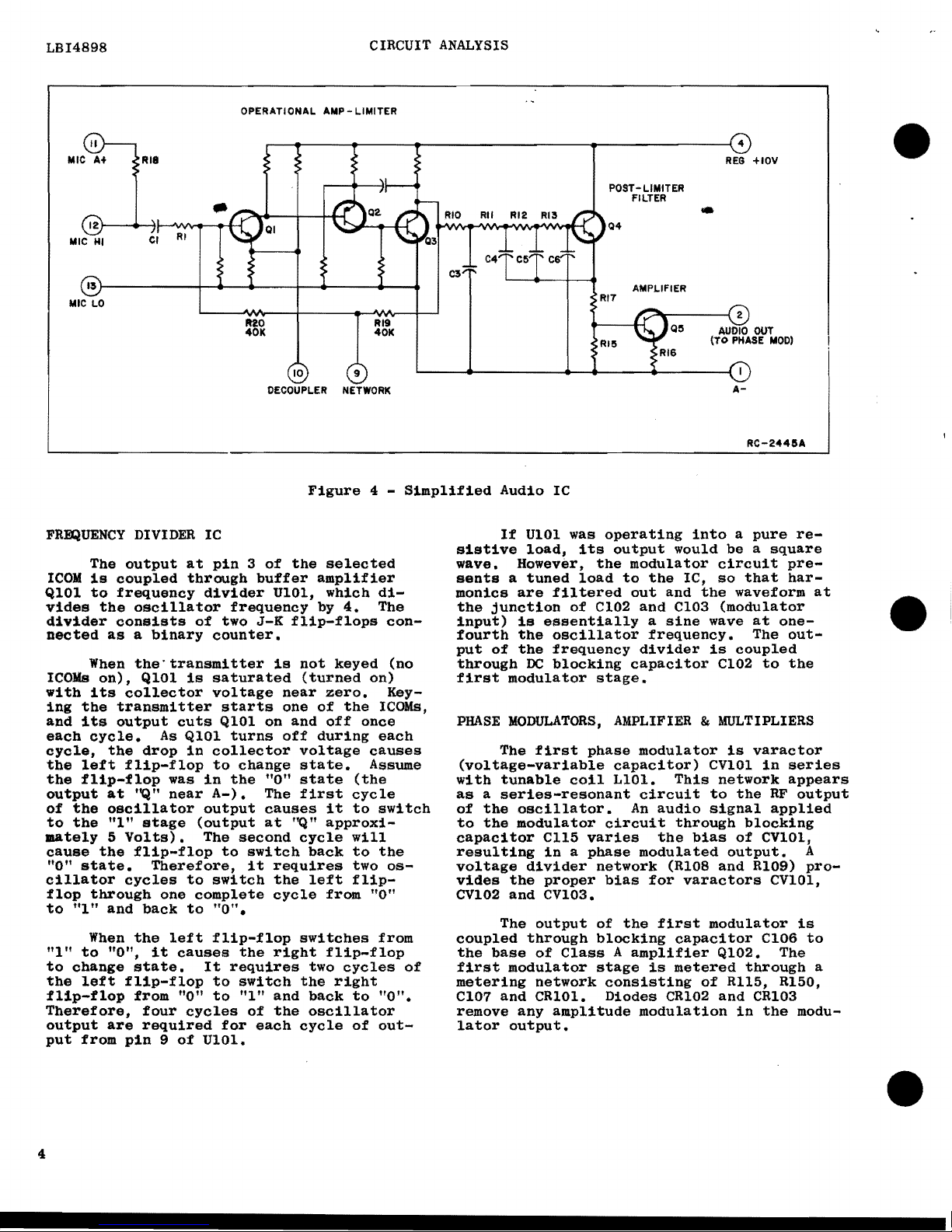
AUDIO
IC
The
transmitter
audio
circuitry
is
con-
tained
in
audio
IC
Ul02.
A
simplified
drawing
of
the
audio
IC
is
shown
in
Figure
4.
Audio
from
the
microphone
at
pin
12
is
coupled
through
pre-emphasis
capacitor
Cl
to
the
base
of
Ql
in
the
operational
amplifier-
limiter
circuit.
Collector
voltage
for
the
transistorized
microphone
preamplifier
is
supplied
from
pin
11
through
microphone
col-
lector
load
resistor
Rl8
to
pin
12.
The
operational
amplifier-limiter
cir-
cuit
consists
of
Ql,
Q2
and
Q3.
Q3
provides
limiting
at
high
signal
levels.
The
gain
of
the
operational
amplifier
circuit
is
fix-
ed
by
negative
feedback
through
Rl9,
R20
and
the
resistance
in
the
network
(pin
9).
The
output
of
Q3
is
coupled
through
a
de-emphasis
network
(RlO
and
C3)
to
an
active
post-limiter
filter
consisting
of
C4,
C5, C6,
Rll,
Rl2,
Rl3,
Rl5,
Rl7,
and
Q4.
Following
the
post-limiter
filter
is
class A amplifier
Q5.
The
output
of
Q5
is
coupled
through
MOD
ADJUST
potentiometer
Rl27
to
the
phase
modulators.
SERVICE
NOTE:
If
the
DC
voltages
to
the
Audio
IC
are
correct
and
no
audio
output
can
be
obtained,
replace
Ul02.
For
radios
equipped
with
Channel
Guard,
tone
from
the
encoder
is
applied
to
the
phase
modulators
through
CHANNEL
GUARD
MOD
ADJUST
potentiometer
Rl28,
and
resistors
RllO,
Rl21
and
Rl24.
Instructions
for
set-
ting
Rl28
are
contained
in
the
modulation
adjustment
section
of
the
Transmitter
Align-
ment
Procedure
•
3
LBI4898
CIRCUIT
ANALYSIS
OPERATIONAL
AMP-
LIMITER
4
MIC
A+
Rl8
REG
+IOV
POST-LIMITER
FILTER
.RIO
Rll
..
Q4
C4
C5
C3
11~--------~~~-4----~~~----._--~
AMPLIFIER
MIC
LO
Rl7
R20
Rlt
401(
40K
Rl5
10
9
OECOUPLER
NETWORK
A-
RC-2445A
Figure
4 -
Simplified
Audio
IC
FREQUENCY
DIVIDER
IC
The
output
at
pin 3 of
the
selected
ICOM
is
coupled
through
buffer
amplifier
QlOl
to
frequency
divider
UlOl,
which
di-
vides
the
oscillator
frequency
by
4.
The
divider
consists
of
two
J-K
flip-flops
con-
nected
as a binary
counter.
When
the·transmitter
is
not
keyed
(no
ICOMs
on),
QlOl
is
saturated
(turned
on)
with
its
collector
voltage
near
zero.
Key-
ing
the
transmitter
starts
one
of
the
ICOMs,
and
its
output
cuts
QlOl
on
and
off
once
each
cycle.
As
QlOl
turns
off
during
each
cycle,
the
drop
in
collector
voltage
causes
the
left
flip-flop
to
change
state.
Assume
the
flip-flop
was
in
the
"O"
state
(the
output
at
''Q"
near
A-).
The
first
cycle
of
the
oscillator
output
causes
it
to
switch
to
the
"1"
stage
(output
at
''Q"
approxi-
mately 5 Volts}.
The
second
cycle
will
cause
the
flip-flop
to
switch
back
to
the
"O"
state.
Therefore,
it
requires
two
os-
cillator
cycles
to
switch
the
left
flip-
flop
through
one
complete
cycle
from
"0"
4
to
"1"
and
back
to
"0"•
When
the
left
flip-flop
switches
from
"1"
to
"O",
it
causes
the
right
flip-flop
to
change
state.
It
requires
two
cycles
of
the
left
flip-flop
to
switch
the
right
flip-flop
from
"O"
to
"1"
and
back
to
"0".
Therefore,
four
cycles
of
the
oscillator
output
are
required
for
each
cycle
of
out-
put
from
pin 9 of
UlOl.
If
UlOl was
operating
into a pure
re-
sistive
load,
its
output
would
be a square
wave. However,
the
modulator
circuit
pre-
sents a tuned
load
to
the
IC,
so
that
har-
monics
are
filtered
out
and
the
waveform
at
the
junction
of
Cl02
and
Cl03
(modulator
input)
is
essentially
a
sine
wave
at
one-
fourth
the
oscillator
frequency.
The
out-
put
of
the
frequency
divider
is
coupled
through
DC
blocking
capacitor
Cl02
to
the
first
modulator
stage.
PHASE
MODULATORS,
AMPLIFIER & MULTIPLIERS
The
first
phase
modulator
is
varactor
(voltage-variable
capacitor)
CVlOl
in
series
with
tunable
coil
LlOl.
This
network
appears
as a series-resonant
circuit
to
the
RF
output
of
the
oscillator.
An
audio
signal
applied
to
the
modulator
circuit
tbrougb
blocking
capacitor
Cll5
varies
the
bias
of
CVlOl,
resulting
in a phase
modulated
output.
A
voltage
divider
network
(Rl08
and
Rl09}
pro-
vides
the
proper
bias
for
varactors
CVlOl,
CV102
and
CV103.
The
output
of
the
first
modulator
is
coupled
through
blocking
capacitor
ClOG
to
the
base
of
Class A amplifier
Ql02.
The
first
modulator
stage
is
metered
through
a
metering
network
consisting
of
Rll5,
Rl50,
Cl07
and
CRlOl.
Diodes
CR102
and
CR103
remove
any
amplitude
modulation
in
the
modu-
lator
output.
•
•
•
 Loading...