

Page 1

LIDAR-Lite v3HP Operation Manual
and Technical Specications
Laser Safety
This device requires no regular maintenance. In the event that the device
becomes damaged or is inoperable, repair or service must be handled by
authorized, factory-trained technicians only. Attempting to repair or service
the unit on your own can result in direct exposure to laser radiation and the
risk of permanent eye damage. For repair or service, contact your dealer or
®
Garmin
for more information. This device has a protective housing which,
when in place, prevents human access to laser radiation in excess of the
accessible emission limit (AEL) for Class 1 laser products. This device should
not be modied or operated without its housing or optics. Operating this device
without a housing and optics, or operating this device with a modied housing
or optics that expose the laser source, may result in direct exposure to laser
radiation and the risk of permanent eye damage. Removal or modication of
the diffuser in front of the laser optic may result in the risk of permanent eye
damage.
This device emits laser radiation. Use of controls or adjustments or
performance of procedures other than those specied herein may result in
hazardous radiation exposure.
This laser product is designated Class 1 during all procedures of operation.
When the ranging feature of the device is activated, a laser emitter of a
ranging module may emit laser radiation and the device should not be aimed
toward anyone. Avoid looking toward the laser emitter or into the laser
radiation (beam) when operating the device. It is advisable to turn off the
ranging module when it is not in use. This device must be used only according
to the directions and procedures described in this documentation.
Do not leave this device within the reach of children.
CLASS 1 LASER PRODUCT
Classied EN/IEC 60825-1 2014
This product is in conformity with performance standards for laser products
under 21 CFR 1040, except with respect to those characteristics authorized by
Variance Number FDA-2016-V-2943 effective September 27, 2016.
WARNING
CAUTION
NOTICE
Table of Contents
LIDAR-Lite v3HP Operation Manual
and Technical Specications ������������������������������������������������������������1
Laser Safety ......................................................................................................1
Specications ������������������������������������������������������������������������������������� 2
Physical .............................................................................................................2
Water Resistance ..............................................................................................2
Electrical ............................................................................................................2
Performance ......................................................................................................2
Interface .............................................................................................................2
Laser ..................................................................................................................2
Connections ���������������������������������������������������������������������������������������� 2
Wiring Harness ..................................................................................................2
I2C Connection Diagrams .................................................................................2
Standard I2C Wiring ....................................................................................2
Standard Arduino I2C Wiring .......................................................................3
PWM Wiring .................................................................................................3
PWM Arduino Wiring....................................................................................3
Operational Information ��������������������������������������������������������������������� 4
Technology ........................................................................................................4
Theory of Operation ...........................................................................................4
Interface .............................................................................................................4
Initialization ..................................................................................................4
Power Enable Pin ........................................................................................4
I2C Interface ................................................................................................4
Mode Control Pin .........................................................................................4
Settings ........................................................................................................4
I2C Protocol Information �������������������������������������������������������������������� 6
I2C Protocol Operation ......................................................................................7
Read Operation ...........................................................................................7
Write Operation ............................................................................................7
Register Denitions ...........................................................................................7
Control Register List ....................................................................................7
Detailed Control Register Denitions ...........................................................8
Frequently Asked Questions ����������������������������������������������������������� 10
How do I use the device for fast-scanning applications? .................................10
Does the device operate only on 5 Vdc? .........................................................10
What is the spread of the laser beam? ............................................................10
How do distance, target size, aspect, and reectivity affect returned signal
strength? ..........................................................................................................10
How does the device work with reective surfaces? ....................................... 11
Diffuse Reective Surfaces ........................................................................ 11
Specular Surfaces .....................................................................................11
How does liquid affect the signal? ................................................................... 11
1
Page 2
Specications
Connections
Physical
Specication Measurement
Size (LxWxH) 20 × 48 × 40 mm (0.8 × 1.9 × 1.6 in.)
Weight 22 g (0.78 oz.)
Operating temperature -20 to 60°C (-4 to 140°F)
Water Resistance
Body of this device is rated IPX7, and can wthstand incidental exposure to
water of up to 1 meter for up to 30 minutes.
IMPORTANT: The bare wire portion of the wiring harness is not water
resistant, and can act as a path for water to enter the device. All bare-wire
connections must either be made in a water-tight location or properly sealed.
Water may enter under the transmitting lens. This could affect performance,
but will not affect IPX7 water resistance.
Electrical
Specication Measurement
Power 5 Vdc nominal
4.5 Vdc min., 5.5 Vdc max.
Current consumption 65 mA idle
85 mA during an acquisition
Performance
Specication Measurement
Range (70% reective target) 40 m (131 ft)
Resolution +/- 1 cm (0.4 in.)
Accuracy < 2 m ±5 cm (2 in.) typical*
Accuracy ≥ 2 m ±2.5 cm (1 in.) typical
Mean ±1% of distance maximum
Ripple ±1% of distance maximum
Update rate (70% Reective Target) Greater than 1 kHz typical
Reduced sensitivity at high update rates
*Nonlinearity present below 1 m (39.4 in.)
Interface
Specication Measurement
User interface I2C
PWM
External trigger
I2C interface Fast-mode (400 kbit/s)
Default 7-bit address 0x62
Internal register access & control
PWM interface External trigger input
PWM output proportional to distance at 10 μs/cm
Laser
Specication Measurement
Wavelength 905 nm (nominal)
Total laser power (peak) 1.3 W
Mode of operation Pulsed (256 pulse max. pulse train)
Pulse width 0.5 μs (50% duty cycle)
Pulse train repetition frequency 10-20 kHz nominal
Energy per pulse <280 nJ
Beam diameter at laser aperture 12 × 2 mm (0.47 × 0.08 in.)
Divergence 8 mRad
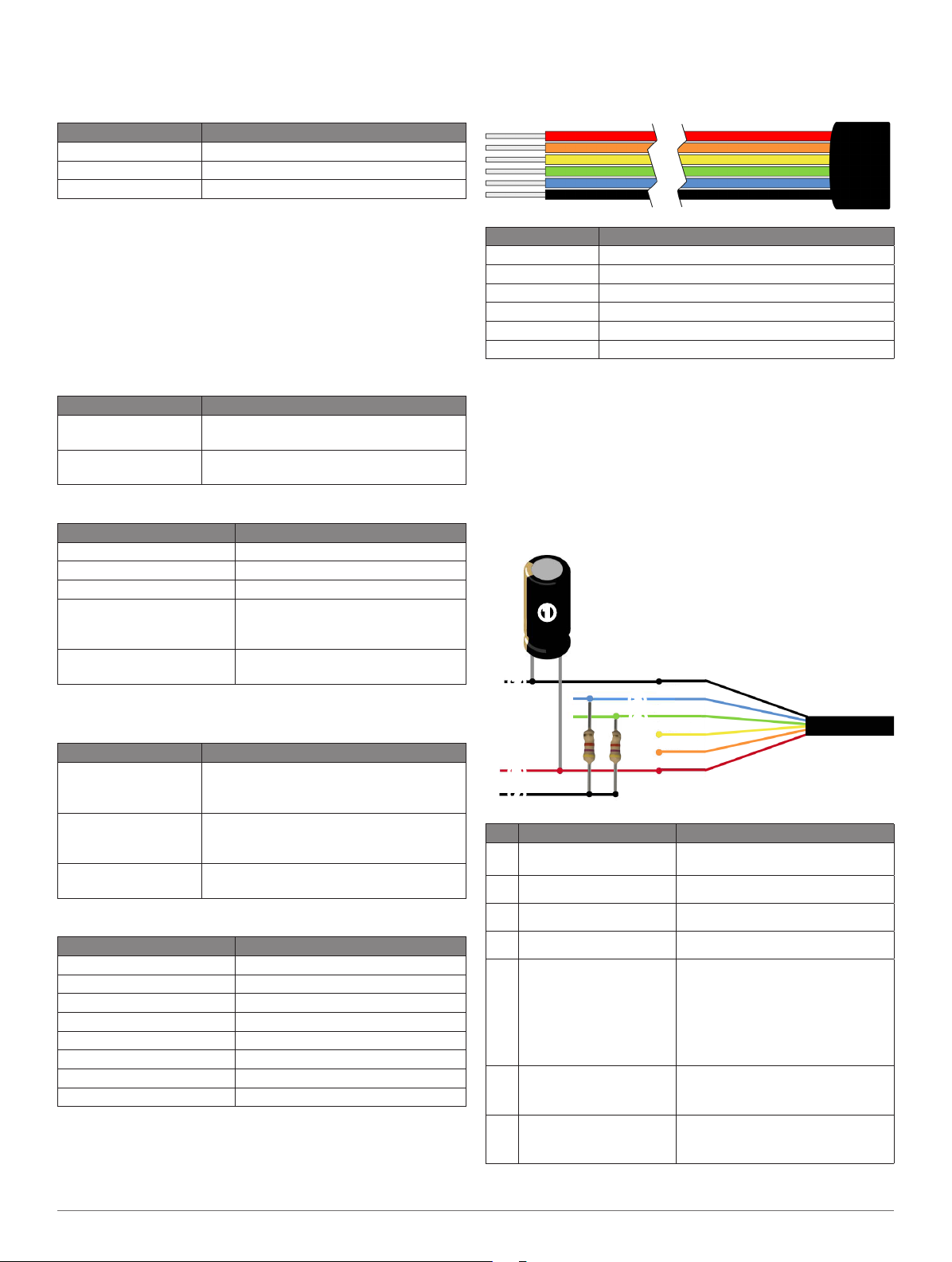
Wiring Harness
Wire Color Function
Red 5 Vdc (+)
Orange Power enable (internal pull-up)
Yellow Mode control
Green I2C SCL
Blue I2C SDA
Black Ground (-)
There are two basic congurations for this device:
• I2C (Inter-Integrated Circuit)—a serial computer bus used to
communicate between this device and a microcontroller, such as an
Arduino board (I2C Interface, page 4).
• PWM (Pulse Width Modulation)—a bi-directional signal transfer method
that triggers acquisitions and returns distance measurements using the
mode-control pin (Mode Control Pin, page 4).
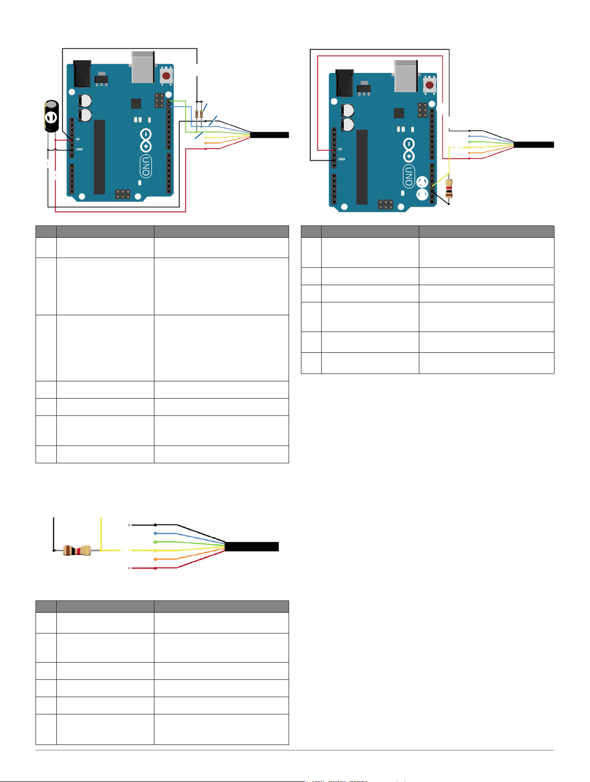
I2C Connection Diagrams
Standard I2C Wiring
➊
➋
➌
➍
➎
➏
➐
Item Description Notes
680µF electrolytic capacitor You must observe the correct polarity when
➊
Power ground (-) connection Black wire
➋
I2C SDA connection Blue wire
➌
I2C SCL connection Green wire
➍
4.7kΩ pull-up resistor
➎
(not required in all applications)
5 Vdc power (+) connection Red wire
➏
Logic rail connection The pull-up resistors connected to both I2C
➐
installing the capacitor.
In installations with long cable extensions
or with multiple devices on the I2C bus, you
must install a 1kΩ to 10kΩ pull-up resistor
on each I2C wire to account for cable
capacitance.
It is recommended to start with 4.7kΩ
resistors and adjust if necessary.
The sensor operates at 4.75 through 5.5 Vdc,
with a max. of 6 Vdc.
wires must connect to the logic rail on your
microcontroller board.
2
Page 3
Standard Arduino I2C Wiring
➊
➋
➌
➍
PWM Arduino Wiring
➊
➋
➎
➐
➏
Item Description Notes
680µF electrolytic capacitor You must observe the correct polarity when
➊
Pull-up resistor connection
➋
(not required in all applications)
4.7kΩ pull-up resistor
➌
(not required in all applications)
I2C SDA connection Blue wire
➍
I2C SCL connection Green wire
➎
5 Vdc power (+) connection Red wire
➏
Power ground (-) connection Black wire
➐
installing the capacitor.
In installations with long cable extensions
or with multiple devices on the I2C bus, you
must connect the pull-up resistors on the
SDA and SCL wires to the logic rail on your
microcontroller board.
On an Arduino board, this is the 5v pin.
In installations with long cable extensions
or with multiple devices on the I2C bus, you
must install a 1kΩ to 10kΩ pull-up resistor
on each I2C wire to account for cable
capacitance.
It is recommended to start with 4.7kΩ
resistors and adjust if necessary.
The sensor operates at 4.75 through 5.5 Vdc,
with a max. of 6 Vdc.
➌
➍
➎
Item Description Notes
5 Vdc power (+) connection Red wire
➊
Power ground (-) connection Black Wire
➋
Mode-control connection Yellow wire
➌
Monitor pin on microcontroller Connect one side of the resistor to the mode-
➍
Trigger pin on microcontroller Connect the other side of the resistor to the
➎
1kΩ resistor
➏
The sensor operates at 4.75 through 5.5 Vdc,
with a max. of 6 Vdc.
control connection on the device, and to a
monitoring pin on your microcontroller board.
trigger pin on your microcontroller board.
➏
PWM Wiring
➊
➋
➌
➍
➎
➏
Item Description Notes
Trigger pin on microcontroller Connect the other side of the resistor to the
➊
Monitor pin on microcontroller Connect one side of the resistor to the mode-
➋
Power ground (-) connection Black Wire
➌
1kΩ resistor
➍
Mode-control connection Yellow wire
➎
5 Vdc power (+) connection Red wire
➏
3
trigger pin on your microcontroller.
control connection on the device, and to a
monitoring pin on your microcontroller.
The sensor operates at 4.75 through 5.5 Vdc,
with a max. of 6 Vdc.
Page 4

Operational Information
Technology
This device measures distance by calculating the time delay between the
transmission of a Near-Infrared laser signal and its reception after reecting off
of a target. This translates into distance using the known speed of light.
Theory of Operation
To take a measurement, this device rst performs a receiver adjustment
routine, correcting for changing ambient light levels and allowing maximum
sensitivity.
The device sends a reference signal directly from the transmitter to the
receiver. It stores the transmit signature, sets the time delay for “zero”
distance, and recalculates this delay periodically after several measurements.
Next, the device initiates a measurement by performing a series of
acquisitions. Each acquisition is a transmission of the main laser signal while
recording the return signal at the receiver. If there is a signal match, the result
is stored in memory as a correlation record. The next acquisition is summed
with the previous result. When an object at a certain distance reects the
laser signal back to the device, these repeated acquisitions cause a peak
to emerge, out of the noise, at the corresponding distance location in the
correlation record.
The device integrates acquisitions until the signal peak in the correlation
record reaches a maximum value. If the returned signal is not strong enough
for this to occur, the device stops at a predetermined maximum acquisition
count.
Signal strength is calculated from the magnitude of the signal record peak
and a valid signal threshold is calculated from the noise oor. If the peak is
above this threshold, the measurement is considered valid and the device will
calculate the distance. Otherwise, it will report 1 cm. When beginning the next
measurement, the device clears the signal record and starts the sequence
again.
Interface
Initialization
On power-up or reset, the device performs a self-test sequence and initializes
all registers with default values. After roughly 22 ms, distance measurements
can be taken with the I2C interface or the Mode Control Pin.
Power Enable Pin
The enable pin uses an internal pullup resistor, and can be driven low to shut
off power to the device.
I2C Interface
This device has a 2-wire, I2C-compatible serial interface (refer to I2CBus Specication, Version 2.1, January 2000, available from Philips
Semiconductor). It can be connected to an I2C bus as a slave device, under
the control of an I2C master device. It supports 400 kHz Fast Mode data
transfer.
The I2C bus operates internally at 3.3 Vdc. An internal level shifter allows the
bus to run at a maximum of 5 Vdc. Internal 3k
functionality and allow for a simple connection to the I2C host.
The device has a 7-bit slave address with a default value of 0x62. The
effective 8-bit I2C address is 0xC4 write and 0xC5 read. The device will not
respond to a general call. Support is not provided for 10-bit addressing.
The most signicant bit of the register is the byte that follows the I2C address
in a normal transaction. Setting this most signicant bit of the I2C address byte
to one triggers automatic incrementing of the register address with successive
reads or writes within an I2C block transfer. This is commonly used to read
the two bytes of a 16-bit value within one transfer and is used in the following
example.
The simplest method of obtaining measurement results from the I2C interface
is as follows:
Write 0x04 to register 0x00.
1
Read register 0x01. Repeat until bit 0 (LSB) goes low.
2
Ω pullup resistors ensure this
Read two bytes from 0x8f (High byte 0x0f then low byte 0x10) to obtain the
3
16-bit measured distance in centimeters.
A list of all available control resisters is available on page 7.
For more information about the I2C protocol, see I2C Protocol Operation
(page 7).
Mode Control Pin
The mode control pin provides a means to trigger acquisitions and return the
measured distance via Pulse Width Modulation (PWM) without having to use
the I2C interface.
The idle state of the mode control pin is high impedance (High-Z). Pulling
the mode control pin low will trigger a single measurement, and the device
will respond by driving the line high with a pulse width proportional to the
measured distance at 10 μs/cm. A 1k
prevent bus contention.
The device drives the mode control pin high at 3.3 Vdc. Diode isolation allows
the pin to tolerate a maximum of 5 Vdc.
As shown in the diagram PWM Arduino Wiring (page 3), a simple
triggering method uses a 1k
the mode control pin low to initiate a measurement, and a host input pin
connected directly to monitor the low-to-high output pulse width.
If the mode control pin is held low, the acquisition process will repeat
indenitely, producing a variable frequency output proportional to distance.
The mode control pin behavior can be modied with the ACQ_CONFIG_REG
(0x04) I2C register as detailed in 0x04 (page 8).
Ω termination resistance is required to
Ω resistor in series with a host output pin to pull
Settings
The device can be congured with alternate parameters for the distance
measurement algorithm. This can be used to customize performance by
enabling congurations that allow choosing between speed, range, and
sensitivity. Other useful features are also detailed in this section. See the full
Control Register List (page 7) for additional settings.
Acquisition Command
Address Name Description Initial Value
0x00 ACQ_COMMAND Device command --
• Writing any non-zero value initiates an acquisition.
Maximum Acquisition Count
Address Name Description Initial Value
0x02 SIG_COUNT_VAL Maximum acquisition count 0xFF
The maximum acquisition count limits the number of times the device will
integrate acquisitions to nd a correlation record peak (from a returned signal),
which occurs at long range or with low target reectivity. This controls the
minimum measurement rate and maximum range. The unit-less relationship
is roughly as follows: rate = 1/n and range = n^(1/4), where n is the number of
acquisitions.
Measurement Quick Termination Detection
Address Name Description Initial Value
0x04 ACQ_CONFIG_REG Acquisition mode control 0x08
You can enable quick-termination detection by clearing bit 3 in this register
(starting with the LSB in this register as bit 0). The device will terminate
a distance measurement early if it anticipates that the signal peak in the
correlation record will reach maximum value. This allows for faster and slightly
less accurate operation at strong signal strengths without sacricing long
range performance.
Detection Sensitivity
Address Name Description Initial Value
0x1c THRESHOLD_
BYPASS
The default valid measurement detection algorithm is based on the peak
value, signal strength, and noise in the correlation record. This can be
overridden to become a simple threshold criterion by setting a non-zero value.
Recommended non-default values are 0x20 for higher sensitivity with more
Peak detection threshold bypass 0x00
4
Page 5

frequent erroneous measurements, and 0x60 for reduced sensitivity and fewer
erroneous measurements.
Congurable I2C Address
Address Name Description Initial Value
0x16 UNIT_ID_HIGH Serial number high byte Unique
0x17 UNIT_ID_LOW Serial number low byte Unique
0x18 I2C_ID_HIGH Write serial number high byte for
I2C address unlock
0x19 I2C_ID_LOW Write serial number low byte for
I2C address unlock
0x1a I2C_SEC_ADDR Write new I2C address after
unlock
0x1e I2C_CONFIG Default address response
control
--
--
--
0x00
The I2C address can be changed from its default value. Available addresses
are 7-bit values with a ‘0’ in the least signicant bit (even hexadecimal
numbers).
To change the I2C address, the unique serial number of the unit must be read
then written back to the device before setting the new address. The process is
as follows:
Read the two byte serial number from 0x96 (high byte 0x16 and low byte
1
0x17).
Write the serial number high byte to 0x18.
2
Write the serial number low byte to 0x19.
3
Write the desired new I2C address to 0x1a.
4
Write 0x08 to 0x1e to disable the default address.
5
This can be used to run multiple devices on a single bus, by enabling one,
changing its address, then enabling the next device and repeating the
process.
The I2C address will be restored to default after a power cycle.
Power Control
Address Name Description Initial Value
0x65 POWER_CONTROL Power state control 0
Setting bit 1 in this register disables the receiver circuit, saving roughly
40 mA. After being re-enabled, the receiver circuit stabilizes by the time a
measurement can be performed.
NOTE: The most effective way to control power usage is to utilize the enable
pin to deactivate the device when not in use.
5
Page 6

I2C Protocol Information
The sensor module has a 7-bit slave address with a default value of 0x62 in hexadecimal notation. The effective 8 bit I2C address is: 0xC4 write, 0xC5 read. The
device will not respond to a general call.
Notes:
• The ACK and NACK items are responses from the master device to the slave device.
• The last NACK in the read is optional, but the formal I2C protocol states that the master shall not acknowledge the last byte.
6
Page 7

I2C Protocol Operation
This protocol description uses the term master to refer to the Arduino
controller, and uses the term LIDAR device to refer to the LIDAR-Lite v3HP
device acting as a slave on the I2C bus.
When working with the I2C serial bus protocol, the device operates as follows:
The master initiates data transfer by establishing a start condition, which
1
consists of a high-to-low transition on the SDA line while SCL is high.
The master sends an address byte, which consists of the 7-bit slave
2
address.
The master sends a read/write bit with a zero state indicating a write
3
request.
A write operation is used as the initial stage of both read and write
transfers.
If the slave address corresponds to the LIDAR device address, the LIDAR
4
device responds by pulling SDA low during the ninth clock pulse.
This operation is considered the acknowledge bit.
At this stage, all other devices on the bus remain idle while the selected
LIDAR device waits for data to be written to or read from its shift register.
Data transmits over the serial bus in sequences of nine clock pulses (eight
5
data bits followed by an acknowledge bit).
These transmissions must occur on the SDA line during the low period of
SCL and remain stable during the high period of SCL.
The master sends an 8-bit data byte following the slave address, which
6
loads the I2C control register on the LIDAR device with the address of the
rst control register to be accessed.
Note: If the high bit (Bit 7) is set, it enables automatic incrementing for
successive reads/writes.
The master requests a read operation from the LIDAR device or sends a
7
write operation to the LIDAR device.
Read Operation
After the master establishes communication with the LIDAR device, obtaining
a reading from the LIDAR device operates as follows.
The rst data frame sets the address of the desired read register. The
1
master sends a stop bit at the completion of the rst data frame.
The master initiates a new start condition, which consists of the slave
2
address with the read bit set (one state).
The master reads one or more data bytes in succession.
3
The LIDAR device sends an acknowledge bit to the master when it
A
receives a valid address.
The master releases the SDA data line with continued clocking of the
B
SCL line.
The master strobes the acknowledge bit and continues the read cycle.
C
After the read cycle is done, the master sends a stop condition to complete
4
the operation.
Write Operation
After the master establishes communication with the LIDAR device, writing to
the LIDAR device operates as follows.
The master sends one or more 8-bit data blocks to the LIDAR device.
1
The LIDAR device sends an acknowledge bit to the master when it
A
receives and writes a valid data byte.
The master releases the SDA data line with continued clocking of the
B
SCL line.
The master strobes the acknowledge bit and continues the write cycle,
C
if necessary.
After the write cycle is done, the master sends a stop condition to complete
3
the operation.
Register Denitions
Control Register List
Address R/W Name Description Intial Value Details
0x00 W ACQ_COMMAND Device command -- page 8
0x01 R STATUS System status -- page 8
0x02 R/W SIG_COUNT_VAL Maximum acquisition count 0xFF page 8
0x04 R/W ACQ_CONFIG_REG Acquisition mode control 0x08 page 8
0x06 W LEGACY_RESET_EN Enables unit reset -- page 8
0x0e R SIGNAL_STRENGTH Received signal strength -- page 8
0x0f R FULL_DELAY_HIGH Distance measurement high byte -- page 8
0x10 R FULL_DELAY_LOW Distance measurement low byte -- page 8
0x12 R/W REF_COUNT_VAL Reference acquisition count 0x03 page 8
0x16 R UNIT_ID_HIGH Serial number high byte Unique page 8
0x17 R UNIT_ID_LOW Serial number low byte Unique page 9
0x18 W I2C_ID_HIGH Write serial number high byte for I2C address unlock -- page 9
0x19 W I2C_ID_LOW Write serial number low byte for I2C address unlock -- page 9
0x1a R/W I2C_SEC_ADDR Write new I2C address after unlock -- page 9
0x1c R/W THRESHOLD_BYPASS Peak detection threshold bypass 0x00 page 9
0x1e R/W I2C_CONFIG Default address response control 0x00 page 9
0x26 R/W PEAK STACK HIGH BYTE Used for post processing of correlation peak data -- page 9
0x27 R/W PEAK STACK LOW BYTE Used for post processing of correlation peak data -- page 9
0x40 R/W COMMAND State command -- page 9
0x48 R HEALTH STATUS Used to diagnose major hardware issues at initialization -- page 10
0x52 R CORR_DATA Correlation record data low byte -- page 10
0x53 R CORR_DATA_SIGN Correlation record data high byte -- page 10
0x65 R/W POWER_CONTROL Power state control 0 page 10
7
Page 8

Detailed Control Register Denitions
NOTE: Unless otherwise noted, all registers contain one byte and are read
and write.
0x00
R/W Name Description Initial Value
W ACQ_COMMAND Device command --
Bit Function
7:1 Write any non-zero value to start a measurement
0 Performs a hard reset by reloading the FPGA and returning all registers to
default values
This operation must be enabled by writing 1 to bit 0 on register 0x06.
When reset the I2C lines go into a high-z state for up to 10 ms. This has the
potential to cause legacy-microcontroller-interface code to crash.
0x01
R/W Name Description Initial Value
R STATUS System status --
Bit Function
5 Health Flag
0: Error detected
1: Reference and receiver bias are operational
4 Device command regulation ag
0: device is not in DC regulation
1: device is in DC regulation
3 Peak detection ag
0: No signal detected
1: Peak detected
2 Reference Overow Flag
0: Reference data has not overowed
1: Reference data in correlation record has reached the maximum value
before overow (occurs periodically)
1 Signal Overow Flag
0: Signal data has not overowed
1: Signal data in correlation record has reached the maximum value before
overow (occurs with a strong received signal strength)
Additional returns can be evaluated using data downloaded from the peak
stack registers, 0x26 and 0x27 (page 9).
0x02
R/W Name Description Initial Value
R/W SIG_COUNT_VAL Maximum acquisition count 0xFF
Bit Function
7:0 Maximum number of acquisitions during measurement
0x04
R/W Name Description Initial Value
R/W ACQ_CONFIG_REG Acquisition mode control 0x08
Bit Function
7 0: Record download resolution set at 9 bits (legacy)
1: Record download resolution set at 12 bits
6 0: Enable reference process during measurement
1: Disable reference process during measurement
5 0: DC compensation enabled
1: DC compensation disabled
4 0: Enable reference lter, averages multiple reference measurements for
increased consistency
1: Disable reference lter
3 0: Enable measurement quick termination. Device will terminate distance
measurement early if it anticipates that the signal peak in the correlation
record will reach maximum value.
1: Disable measurement quick termination.
2 bit unused
1:0 Mode Select Pin Function Control
00: Default PWM mode. Pull pin low to trigger measurement, device will
respond with an active high output with a duration of 10us/cm.
01: Status output mode. Device will drive pin active high while busy. Can be
used to interrupt host device.
10: Fixed delay PWM mode. Pulling pin low will not trigger a measurement.
11: Oscillator output mode. Nominal 31.25 kHz output. The accuracy of the
silicon oscillator in the device is generally within 1% of nominal. This affects
distance measurements proportionally and can be measured to apply a
compensation factor.
0x06
R/W Name Description Initial Value
R LEGACY_RESET_EN Enables legacy unit reset --
Bit Function
0 Writing 1 to bit 0 enables the legacy reset operation using the 0x00 register.
0x0e
R/W Name Description Initial Value
R SIGNAL_STRENGTH Received signal strength --
Bit Function
7:0 Received signal strength calculated from the value of the highest peak in the
correlation record and how many acquisitions were performed.
0x0f
R/W Name Description Initial Value
R FULL_DELAY_HIGH Distance measurement high byte --
Bit Function
7:0 Distance measurement result in centimeters, high byte.
0x10
R/W Name Description Initial Value
R FULL_DELAY_LOW Distance measurement low byte --
Bit Function
7:0 Distance measurement result in centimeters, low byte.
0x12
R/W Name Description Initial Value
R/W REF_COUNT_VAL Reference acquisition count 0x03
Bit Function
7:0 Non-default number of reference acquisitions during measurement. ACQ_
CONFIG_REG (0x04) bit 2 must be set.
0x16
R/W Name Description Initial Value
R UNIT_ID_HIGH Serial number high byte Unique
Bit Function
7:0 Unique serial number of device, high byte.
8
Page 9

0x17
R/W Name Description Initial Value
R UNIT_ID_LOW Serial number low byte Unique
0x1e
R/W Name Description Initial Value
R/W I2C_CONFIG Default address response control 0x00
Bit Function
7:0 Unique serial number of device, high byte.
0x18
R/W Name Description Initial Value
W I2C_ID_HIGH Write serial number high byte for I2C
address unlock
Bit Function
7:0 Write the value in UNIT_ID_HIGH (0x16) here as part of enabling a non-
default I2C address. See I2C_ID_LOW (0x19) and I2C_SEC_ADDR (0x1a).
--
0x19
R/W Name Description Initial Value
W I2C_ID_LOW Write serial number low byte for I2C
address unlock
Bit Function
7:0 Write the value in UNIT_ID_LOW (0x17) here as part of enabling a non-default
I2C address. See I2C_ID_HIGH (0x18) and I2C_SEC_ADDR (0x1a).
--
0x1a
R/W Name Description Initial Value
R/W I2C_SEC_ADDR Write new I2C address after unlock --
Bit Function
7:0 Non-default I2C address.
Available addresses are 7-bit values with a ‘0’ in the least signicant bit (even
hexadecimal numbers).
I2C_ID_HIGH (0x18) and I2C_ID_LOW (0x19) must have the correct value for
the device to respond to the non-default I2C address.
0x1c
R/W Name Description Initial Value
R/W THRESHOLD_
BYPASS
Bit Function
7:0 0x00: Use default valid measurement detection algorithm based on the peak
value, signal strength, and noise in the correlation record.
0x01-0xff: Set simple threshold for valid measurement detection. Values 0x200x60 generally perform well.
Peak detection threshold bypass 0x00
Bit Function
5 0: Disables the alternate status mode.
1: Enables an alternate indication status byte at STATUS register 0x01.
NOTE: If bit 5 is enabled (1), the status word consists of all ones except for
the bit position selected by bits [2:0] in this I2C CONFIG register (0x1e). This
allows for the reading of the busy status of multiple units sharing the same
active base address 0x62.
4 0: Disables the altrenative I2C address.
1: Enables the alternative I2C address.
3 0: Device will respond to I2C address 0x62. Device will also respond to
non-default address if congured successfully. See I2C_ID_HIGH (0x18),
I2C_ID_LOW (0x19), and I2C_SEC_ADDR (0x1a).
1: Device will only respond to non-default I2C address. It is recommended to
congure the non-default address rst, then use the non-default address to
write to this register, ensuring success.
2:0 Denes the bit position(s) to remain set as 0 when bit 5 is enabled.
0x26
R/W Name Description Initial Value
R/W PEAK STACK
HIGH BYTE
Bit Function
10:8 For every 11-bit stack value, this resister (0x26) must be read rst. Reading
from this register latches the low order data into 0x27 and increments the
stack pointer.
Writing 0x01 to this register (0x26) resets the stack pointer to the rst element.
Registers read successive values
from the peak stack register. Data
from the stack register is used for post
processing.
--
0x27
R/W Name Description Initial Value
R/W PEAK STACK
LOW BYTE
Bit Function
7:0 Reading from 0x27 reads the low order data from this register.
Registers read successive values
from the peak stack register. Data
from the stack register is used for post
processing.
--
0x40
R/W Name Description Initial Value
R/W TEST COMMAND State command --
Bit Function
2:0 000: Test mode disable, resume normal operation
111: Test mode enable, allows download of correlation record
Once test mode is enabled, read CORR_DATA (0x52) and CORR_DATA_
SIGN (0x53) in one transaction (read from 0xd2). The memory index is
incremented automatically and successive reads produce sequential data.
9
Page 10

0x48
R/W Name Description Initial Value
R HEALTH STATUS Used to diagnose major hardware issues
at system initialization.
Bit Function
4:0 Reference value is within normal range.
3 Reference overow occurred during the rst acquisition.
2 An initial acquisition was completed at wake-up to set the initial reference
value.
1 The receiver DC control command is within the normal range.
0 DC regulation was successful during wake-up.
--
0x52
R/W Name Description Initial Value
R CORR_DATA Correlation record data low byte --
Bit Function
7:0 Correlation record data low byte. See CORR_DATA_SIGN (0x53), ACQ_
SETTINGS (0x5d), and COMMAND (0x40).
0x53
R/W Name Description Initial Value
R CORR_DATA_SIGN Correlation record data high byte --
Bit Function
7:0 Correlation record data high byte. Correlation record data is a 2’s complement
9-bit value, and must be sign extended to be formatted as a 16-bit 2’s
complement value. Thus when repacking the two bytes obtained for the I2C
transaction, set the high byte to 0xff if the LSB of the high byte is one.
0x65
R/W Name Description Initial Value
R/W POWER_CONTROL Power state control 0x80
Bit Function
0 1: Disable receiver circuit
0: Enable receiver circuit. Receiver circuit stabilizes by the time a
measurement can be performed.
Frequently Asked Questions
How do I use the device for fast-scanning applications?
Using the LIDAR-Lite v3HP device for fast-scanning applications may
require you to change the program you used for “continuous” or “burst” mode
functions with previous versions of the sensor.
Initiate new measurement command.
1
Immediately read the distance registers, obtaining the previous
2
measurement results while the new measurement is occurring.
Measurement data stored in the sensor is valid until a new measurement
concludes.
Perform other actions while polling the status bit until it indicates an idle
3
state.
Repeat steps 1 through 3.
4
NOTES:
• This method uses slightly more I2C overhead, but it allows more efcient
polling if you know about your measurement time, which depends on
maximum acquisition count settings. You also know exactly when that
measurement begins.
• With this approach (and nothing else going on except relentless polling),
the device has been able to reach >1.5 kHz with very small acquisition
count settings.
• You can nd sample Arduinio code for this in the Garmin GitHub
repository at the following location: https://github.com/garmin/LIDARLite_
v3_Arduino_Library/blob/master/examples/ShortRangeHighSpeed/
ShortRangeHighSpeed.ino.
Does the device operate only on 5 Vdc?
The device requires 5 Vdc to function properly.
Connecting the device to a source greater or less than 5 Vdc is not supported,
and may result in poor performance or may damage the device.
What is the spread of the laser beam?
At very close distances (less than 1 m), the beam diameter is about the size
of the aperture (lens). For distances greater than 1 m, you can estimate the
beam diameter using this equation:
Distance/100 = beam diameter at that distance (in whatever units you
measured the distance).
The actual spread is ~8 milli radians or ~1/2 degree.
NOTICE
How do distance, target size, aspect, and reectivity
affect returned signal strength?
The device transmits a focused infrared beam that reects off of a target,
and a portion of that reected signal returns to the receiver. The distance is
calculated by taking the difference between the moment of signal transmission
to the moment of signal reception. Successfully receiving a reected signal is
heavily inuenced by several factors. These factors include:
• Target Distance
The relationship of distance (D) to returned signal strength is an inverse
square. With an increase in distance, the returned signal strength
decreases by 1/D^2 or the square root of the distance.
• Target Size
The relationship of a target’s Cross Section (C) to returned signal strength
is an inverse power of four. The device transmits a focused near-infrared
laser beam that spreads at a rate of approximately 0.5º as distance
increases. Up to 1 m, it is approximately the size of the lens. Beyond 1 m,
the approximate beam spread in degrees can be estimated by dividing the
distance by 100, or ~8 milliradians. When the beam overlls (is larger than)
the target, the signal returned decreases by 1/C^4 or the fourth root of the
target’s cross section.
10
Page 11

• Aspect
The aspect of the target, or its orientation to the sensor, affects the
observable cross section and, therefore, the amount of returned signal
decreases as the aspect of the target varies from the normal.
• Reectivity
Reectivity characteristics of the target’s surface also affect the amount
of returned signal (How does the device work with reective surfaces?,
page 11).
In summary, a small target can be very difcult to detect if it is distant, poorly
reective, and its aspect is away from the normal. In such cases, the returned
signal strength may be improved by attaching infrared reectors to the target,
increasing the size of the target, modifying its aspect, or reducing distance
from the sensor.
How does the device work with reective surfaces?
Reective characteristics of an object’s surface can be divided into three
categories:
• Diffuse Reective
• Specular
• Retro-reective
Diffuse Reective Surfaces
Purely diffuse surfaces are found on materials that have a textured quality
that causes reected energy to disperse uniformly. This tendency results in a
relatively predictable percentage of the dispersed laser energy nding its way
back to the device. As a result, these materials tend to read very well.
Materials that fall into this category are paper, matte walls, and granite. It
is important to note that materials that t into this category due to observed
reection at visible light wavelengths may exhibit unexpected results in other
wavelengths. The near infrared range used by the device may detect them
as nearly identical. For example, a black sheet of paper may reect a nearly
identical percentage of the infrared signal back to the receiver as a white
sheet.
How does liquid affect the signal?
There are a few considerations to take into account if your application requires
measuring distances to, or within, liquid:
• Reectivity and other characteristics of the liquid itself
• Reectivity characteristics of particles suspended in the liquid
• Turbidity
• Refractive characteristics of the liquid
Reectivity of the liquid is important when measuring distance to the surface of
a liquid or if measuring through liquid to the bottom of a container (How does
the device work with reective surfaces?, page 11).
Measuring distance with the device depends on reected energy from the
transmitted signal being detected by the receiver in the sensor. For that
reason, the surface condition of the liquid may play an important role in
the overall reectivity and detectability of the liquid. In the case of a at,
highly reective liquid surface, the laser’s reected energy may not disperse
adequately to allow detection unless viewed from the normal. By contrast,
small surface ripples may create enough dispersion of the reected energy to
allow detection of the liquid without the need to position the sensor so that the
transmitted beam strikes the liquid’s surface from the normal.
Reectivity of suspended particles is a characteristic that may help or hinder,
depending on the application.
Turbidity, or the clarity of a liquid created by the presence or absence of
suspended particles, can similarly help or hinder measurement efforts. If
the application requires detecting the surface of the liquid, then suspended
particles may help by reecting more of the transmitted beam back to the
receiver, increasing detectability and permitting measurements to be taken.
Attempting to measure through suspended particles in a liquid will only be
successful if the transmitted beam is allowed to reect off of the desired target
without rst being absorbed or reected by the suspended particles.
When the near infrared energy transmitted by the device transitions from the
atmosphere to a liquid, the energy may be bent, or refracted, and absorbed
in addition to being dispersed. The degree to which the transmitted beam is
refracted and absorbed is dened by its refraction index. That being said, the
most important criteria impacting successful measurement through a liquid
is the amount of dispersion of the transmitted beam and whether any of the
dispersed beam makes its way back to the receiver on the device.
Electromagnetic energy travels slower through a liquid and may affect
accuracy of the nal measurement output.
Specular Surfaces
Specular surfaces, are found on materials that have a smooth quality that
reect energy instead of dispersing it. It is difcult or impossible for the
device to recognize the distance of many specular surfaces. Reections
off of specular surfaces tend to reect with little dispersion which causes
the reected beam to remain small and, if not reected directly back to the
receiver, to miss the receiver altogether. The device may fail to detect a
specular object in front of it unless viewed from the normal.
Examples of specular surfaces are mirrors and glass viewed off-axis.
11
Page 12

© 2018 Garmin Ltd. or its subsidiaries
1200 East 151st Street, Olathe, Kansas 66062, USA
Liberty House, Hounsdown Business Park, Southampton, Hampshire, SO40 9LR UK
No. 68, Zhangshu 2nd Road, Xizhi Dist., New Taipei City, 221, Taiwan (R.O.C.)
April 2018 190-02088-02_0A
Garmin International, Inc.
Garmin (Europe) Ltd.
Garmin Corporation
www.garmin.com
 Loading...