


FUJITSU SEMICONDUCTOR
DATA SHEET
FLASH MEMORY
CMOS
DS05-20880-1E
16M (2M × 8/1M × 16) BIT
MBM29DL16XTE/BE
FEATURES
■
• 0.23 µm Process Technology
• Simultaneous Read/Write operations (dual bank)
Multiple devices available with different bank sizes (Refer to Table 1)
Host system can program or erase in one bank, then immediately and simultaneously read from the other bank
Zero latency between read and write operations
Read-while-erase
Read-while-program
• Single 3.0 V read, program, and erase
Minimizes system level power requirements
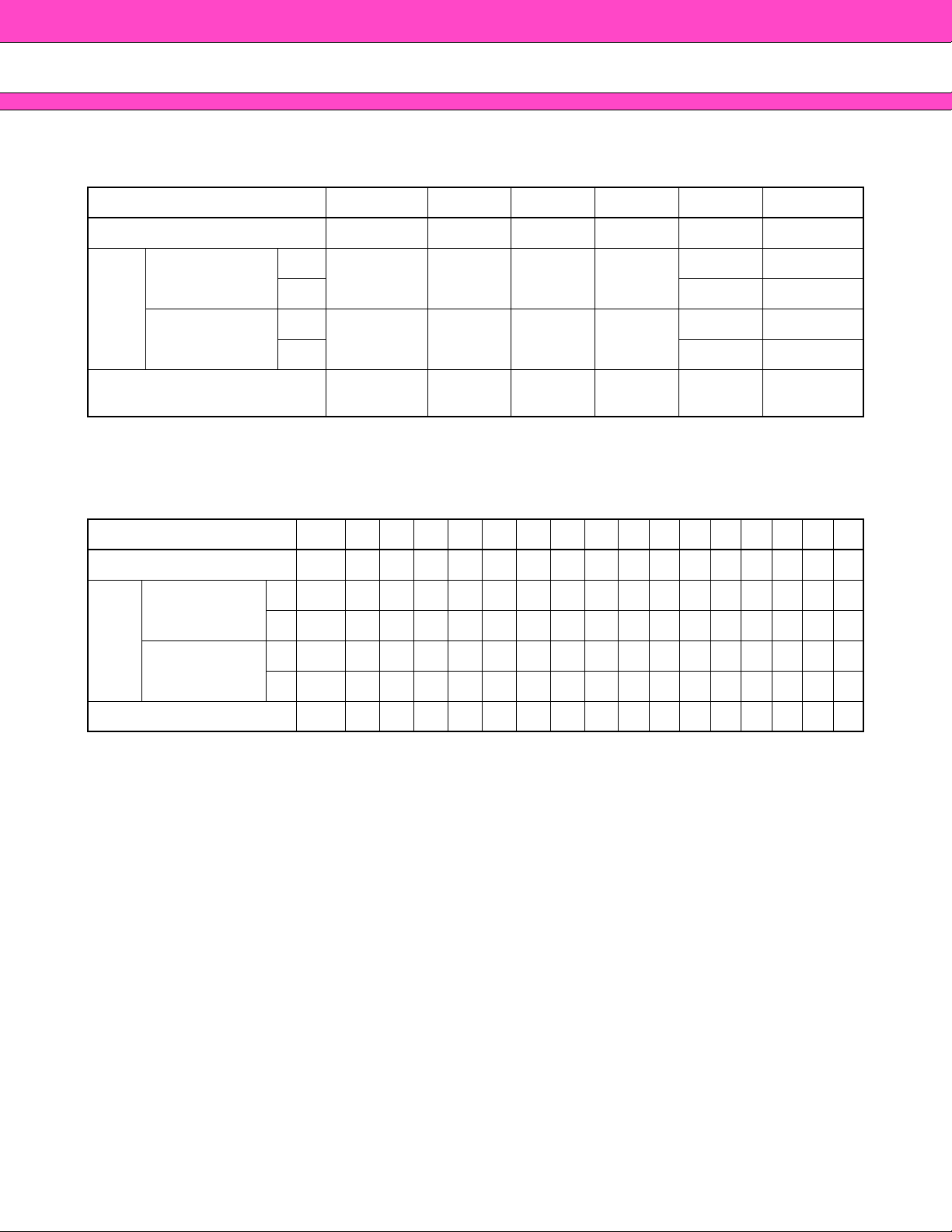
PRODUCT LINE UP
■
Part No. MBM29DL16XTE/BE
V
Ordering Part No.
Max. Address Access Time (ns) 70 90 120
CC = 3.3 V
V
CC = 3.0 V
+0.3 V
–0.3 V
+0.6 V
–0.3 V
-70/90/12
70 — —
—9012
Dual Operation
(Continued)
Max. CE
Max. OE
PACKAGES
■
48-pin plastic TSOP (I)
Access Time (ns) 70 90 120
Access Time (ns) 30 35 50
Marking Side
(FPT-48P-M19)
48-pin plastic TSOP (I)
Marking Side
(FPT-48P-M20)
48-pin plastic FBGA
(BGA-48P-M11)

MBM29DL16XTE/BE
-70/90/12
(Continued)
• Compatible with JEDEC-standard commands
Uses same software commands as E
2
PROMs
• Compatible with JEDEC-standard world-wide pinouts
48-pin TSOP(I) (Package suffix: TN – Normal Bend Type, TR – Reversed Bend Type)
48-ball FBGA (Package suffix: PBT)
• Minimum 100,000 program/erase cycles
• High performance
70 ns maximum access time
• Sector erase architecture
Eight 4K word and thirty one 32K word sectors in word mode
Eight 8K byte and thirty one 64K byte sectors in byte mode
Any combination of sectors can be concurrently erased. Also supports full chip erase.
• Boot Code Sector Architecture
T = Top sector
B = Bottom sector
• Hidden ROM (Hi-ROM) region
64K byte of Hi-ROM, accessible through a new “Hi-ROM Enable” command sequence
Factory serialized and protected to provide a secure electronic serial number (ESN)
/ACC input pin
•WP
At V
IL, allows protection of boot sectors, regardless of sector protection/unprotection status
At V
IH, allows removal of boot sector protection
ACC
At V
• Embedded Erase
, increases program performance
TM
* Algorithms
Automatically pre-programs and erases the chip or any sector
• Embedded Program
TM
* Algorithms
Automatically writes and verifies data at specified address
•Data
Polling and Toggle Bit feature for detection of program or erase cycle completion
• Ready/Busy output (RY/BY)
Hardware method for detection of program or erase cycle completion
• Automatic sleep mode
When addresses remain stable, automatically switch themselves to low power mode.
•Low V
CC
write inhibit ≤ 2.5 V
• Program Suspend/Resume
Suspends the program operation to allow a read in another sector with in the same device
• Erase Suspend/Resume
Suspends the erase operation to allow a read data and/or program in another sector within the same device
• Sector group protection
Hardware method disables any combination of sector groups from program or erase operations
• Sector Group Protection Set function by Extended sector group protection command
• Fast Programming Function by Extended Command
• Temporary sector group unprotection
Temporary sector group unprotection via the RESET
• In accordance with CFI (C
ommon Flash Memory Interface)
pin.
Embedded EraseTM and Embedded ProgramTM are trademarks of Advanced Micro Devices, Inc.
* :
2

MBM29DL16XTE/BE
GENERAL DESCRIPTION
■
The MBM29DL16XTE/BE are a 16M-bit, 3.0 V-only Flash memory organized as 2M b ytes of 8 bits each or 1M
words of 16 bits each. The MBM29DL16XTE/BE are offered in a 48-pin TSOP(I) and 48-ball FBGA Package.
These devices are designed to be programmed in-system with the standard system 3.0 V VCC supply. 12.0 V
V
PP and 5.0 V VCC are not required for write or erase operations. The devices can also be reprogrammed in
standard EPROM programmers.
MBM29DL16XTE/BE are organized into two banks, Bank 1 and Bank 2, which can be considered to be two
separate memory arrays as far as certain operations are concerned. These devices are the same as Fujitsu’s
standard 3 V only Flash memories with the additional capability of allowing a normal non-delayed read access
from a non-busy bank of the array while an embedded write (either a program or an erase) operation is
simultaneously taking place on the other bank.
In the MBM29DL16XTE/BE, a new design concept is implemented, so called “Sliding Bank Architecture”. Under
this concept, the MBM29DL16XTE/BE can be produced a series of devices with different Bank 1/Bank 2 size
combinations; 0.5 Mb/15.5 Mb, 2 Mb/14 Mb, 4 Mb/12 Mb, 8 Mb/8 Mb.
The standard MBM29DL16XTE/BE offer access times 70 ns, 90 ns and 120 ns, allo wing operation of high-speed
microprocessors without wait states. To eliminate bus contention the devices have separate chip enable (CE
write enable (WE), and output enable (OE) controls.
The MBM29DL16XTE/BE are pin and command set compatible with JEDEC standard E
are written to the command register using standard microprocessor write timings. Register contents serve as
input to an internal state-machine which controls the erase and programming circuitry . Write cycles also internally
latch addresses and data needed for the programming and erase operations. Reading data out of the devices
is similar to reading from 5.0 V and 12.0 V Flash or EPROM devices.
2
PROMs. Commands
-70/90/12
),
The MBM29DL16XTE/BE are programmed by e x ecuting the progr am command sequence. This will in v ok e the
Embedded Program Algorithm which is an internal algorithm that automatically times the program pulse widths
and verifies proper cell margin. Typically, each sector can be programmed and verified in about 0.5 seconds.
Erase is accomplished by executing the erase command sequence. This will invoke the Embedded Erase
Algorithm which is an internal algorithm that automatically preprograms the array if it is not already programmed
before e xecuting the erase operation. During erase, the devices automatically time the erase pulse widths and
verify proper cell margin.
A sector is typically erased and verified in 1.0 second. (If already completely preprogrammed.)
The devices also feature a sector erase architecture. The sector mode allows each sector to be erased and
reprogrammed without affecting other sectors. The MBM29DL16XTE/BE are erased when shipped from the
factory .
The devices f eature single 3.0 V pow er supply operation f or both read and write functions. Internally generated
and regulated voltages are provided for the program and erase operations. A low V
inhibits write operations on the loss of power. The end of program or erase is detected by Data Polling of DQ7,
by the Toggle Bit feature on DQ6, or the RY/BY output pin. Once the end of a program or erase cycle has been
completed, the devices internally reset to the read mode.
Fujitsu’s Flash technology combines years of EPROM and E
of quality , reliability , and cost eff ectiveness. The MBM29DL16XTE/BE memories electrically erase the entire chip
or all bits within a sector simultaneously via Fowler-Nordhiem tunneling. The b ytes/words are prog rammed one
byte/word at a time using the EPROM programming mechanism of hot electron injection.
2
PROM experience to produce the highest levels
CC detector automatically
3

MBM29DL16XTE/BE
Table 1 MBM29DL16XTE/BE Device Bank Divisions
-70/90/12
Device
Part Number
MBM29DL161TE/BE
MBM29DL162TE/BE 2 Mbit
MBM29DL163TE/BE 4 Mbit
MBM29DL164TE/BE 8 Mbit
Organization
Megabits Sector Sizes Megabits Sector Sizes
0.5 Mbit Eight 8K byte/4K word 15.5 Mbit
× 8/× 16
Bank 1 Bank 2
Eight 8K byte/4K word,
three 64K byte/32K word
Eight 8K byte/4K word,
seven 64K byte/32K word
Eight 8K byte/4K word,
fifteen 64K byte/32K word
14 Mbit
12 Mbit
8 Mbit
Thirty-one
64K byte/32K word
Twenty-eight
64K byte/32K word
Twenty-four
64K byte/32K word
Sixteen
64K byte/32K word
4

PIN ASSIGNMENTS
■
MBM29DL16XTE/BE
TSOP(I)
-70/90/12
A15
A14
A13
A12
A11
A10
A9
A8
A19
N.C.
WE
RESET
N.C.
WP/ACC
RY/BY
A
A17
A7
A6
A5
A4
A3
A2
A1
A1
A2
A3
A4
A5
A6
A7
A17
A18
RY/BY
WP/ACC
N.C.
RESET
WE
N.C.
A
A8
A9
A10
A11
A12
A13
A14
A15
1
2
3
4
5
6
7
8
9
10
11
12
13
14
15
18
16
17
18
19
20
21
22
23
24
24
23
22
21
20
19
18
17
16
15
14
13
12
11
10
19
9
8
7
6
5
4
3
2
1
(Marking Side)
Standard Pinout
(FPT-48P-M19)
(Marking Side)
Reverse Pinout
(FPT-48P-M20)
48
47
46
45
44
43
42
41
40
39
38
37
36
35
34
33
32
31
30
29
28
27
26
25
25
26
27
28
29
30
31
32
33
34
35
36
37
38
39
40
41
42
43
44
45
46
47
48
A16
BYTE
VSS
DQ15/A-1
DQ7
DQ14
DQ6
DQ13
DQ5
DQ12
DQ4
VCC
DQ11
DQ3
DQ10
DQ2
DQ9
DQ1
DQ8
DQ0
OE
V
SS
CE
A
0
A0
CE
V
SS
OE
DQ
0
DQ8
DQ1
DQ9
DQ2
DQ10
DQ3
DQ11
VCC
DQ4
DQ12
DQ5
DQ13
DQ6
DQ14
DQ7
DQ15/A-1
VSS
BYTE
A16
(Continued)
5

MBM29DL16XTE/BE
-70/90/12
(Continued)
FBGA
(TOP VIEW)
Marking side
A1 A2 A3 A4 A5 A6
B1 B2 B3 B4 B5 B6
C1 C2 C3 C4 C5 C6
D1 D2 D3 D4 D5 D6
E1 E2 E3 E4 E5 E6
F1 F2 F3 F4 F5 F6
G1 G2 G3 G4 G5 G6
H1 H2 H3 H4 H5 H6
(BGA-48P-M11)
A1 A3 A2 A7 A3 RY/BY A4 WE A5 A9 A6 A13
B1 A4 B2 A17 B3 WP/ACC B4 RESET B5 A8 B6 A12
C1 A2 C2 A6 C3 A18 C4 N.C. C5 A10 C6 A14
D1 A1 D2 A5 D3 N.C. D4 A19 D5 A11 D6 A15
E1 A0 E2 DQ0 E3 DQ2 E4 DQ5 E5 DQ7 E6 A16
F1 CE F2 DQ8 F3 DQ10 F4 DQ12 F5 DQ14 F6 BYTE
G1 OE G2 DQ9 G3 DQ11 G4 VCC G5 DQ13 G6 DQ15/A-1
H1 VSS H2 DQ1 H3 DQ3 H4 DQ4 H5 DQ6 H6 VSS
6

BLOCK DIAGRAM
■
VCC
VSS
MBM29DL16XTE/BE
-70/90/12
A
0 to A19
(A-1)
RESET
WE
CE
OE
BYTE
WP/ACC
DQ0 to DQ15
State
Control
&
Command
Register
Bank 2 Address
RY/BY
Status
Bank 1 Address
Control
Cell Matrix
(Bank 2)
X-Decoder
X-Decoder
Cell Matrix
(Bank 1)
Y-Gating & Data Latch
Y-Gating &
Data Latch
DQ0 to DQ15
7

MBM29DL16XTE/BE
LOGIC SYMBOL
■
-70/90/12
Table 2 MBM29DL16XTE/BE Pin Configuration
Pin Function
20
A-1
A0 to A19
CE
OE
WE
RESET
BYTE
WP/ACC
DQ0 to DQ15
RY/BY
16 or 8
A
-1, A0 to A19 Address Inputs
0 to DQ15 Data Inputs/Outputs
DQ
CE
OE
WE
RY/BY
RESET
BYTE
WP
/ACC
Chip Enable
Output Enable
Write Enable
Ready/Busy Output
Hardware Reset Pin/Temporary Sector
Group Unprotection
Selects 8-bit or 16-bit mode
Hardware Write Protection/Program
Acceleration
N.C. No Internal Connection
SS Device Ground
V
CC Device Power Supply
V
8

DEVICE BUS OPERATION
■
Table 3 MBM29DL16XTE/BE User Bus Operations (BYTE
MBM29DL16XTE/BE
= VIH)
-70/90/12
Operation CE
Auto-Select Manufacturer Code (1) L L H L L L V
Auto-Select Device Code (1) L L H H L L V
Read (3) L L H A
OE WE A0A1A6A9DQ0 to DQ15RESET WP/ACC
ID Code H X
ID Code H X
0 A1 A6 A9 DOUT HX
Standby HXXXXXX HIGH-Z H X
Output Disable L H H X X X X HIGH-Z H X
Write (Program/Erase) L H L A
Enable Sector Group Protection (2), (4) L V
ID LHLVID XHX
Verify Sector Group Protection (2), (4) L L H L H L V
Temporary Sector Group Unprotection (5) XXXXXXX X V
0 A1 A6 A9 DIN HX
ID Code H X
ID X
Reset (Hardware)/Standby XXXXXXX HIGH-Z L X
Boot Block Sector Write Protection XXXXXXX X X L
Table 4 MBM29DL16XTE/BE User Bus Operations (BYTE
Operation CE
OE WE
DQ15/
-1
A
A0A1A6A9DQ0 to DQ7RESET WP/ACC
Auto-Select Manufacturer Code (1) L L H L L L L V
Auto-Select Device Code (1) L L H L H L L V
= VIL)
ID Code H X
ID Code H X
Read (3) L L H A
-1 A0 A1 A6 A9 DOUT HX
Standby HXXX XXXX HIGH-Z H X
Output Disable L H H X X X X X HIGH-Z H X
Write (Program/Erase) L H L A
Enable Sector Group Protection
(2), (4)
Verify Sector Group Protection
(2), (4)
Temporary Sector Group
Unprotection (5)
ID LLHLVID XHX
LV
LLHLLHLV
XXX X XXXX X V
-1 A0 A1 A6 A9 DIN HX
ID Code H X
ID X
Reset (Hardware)/Standby X X X X X X X X HIGH-Z L X
Boot Block Sector Write Protection X X X X X X X X X X L
L = V
Legend:
IL, H = VIH, X = VIL or VIH, = Pulse input. See DC Characteristics for voltage levels.
Notes: 1. Manufacturer and device codes may also be accessed via a command register write sequence. See
Table 12.
2. Refer to the section on Sector Group Protection.
3. WE
can be VIL if OE is VIL, OE at VIH initiates the write operations.
4. VCC = 3.3 V ± 10%
5. It is also used for the extended sector group protection.
9

MBM29DL16XTE/BE
FLEXIBLE SECTOR-ERASE ARCHITECTURE
■
Table 5.1 Sector Address Tables (MBM29DL161TE)
Sector Address
Bank Sector
SA0 00000XXX64/32000000H to 00FFFFH 000000H to 007FFFH
SA1 00001XXX64/32010000H to 01FFFFH 008000H to 00FFFFH
SA2 00010XXX64/32020000H to 02FFFFH 010000H to 017FFFH
SA3 00011XXX64/32030000H to 03FFFFH 018000H to 01FFFFH
SA4 00100XXX64/32040000H to 04FFFFH 020000H to 027FFFH
SA5 00101XXX64/32050000H to 05FFFFH 028000H to 02FFFFH
SA6 00110XXX64/32060000H to 06FFFFH 030000H to 037FFFH
SA7 00111XXX64/32070000H to 07FFFFH 038000H to 03FFFFH
SA8 01000XXX64/32080000H to 08FFFFH 040000H to 047FFFH
SA9 01001XXX64/32090000H to 09FFFFH 048000H to 04FFFFH
SA1001010XXX64/320A0000H to 0AFFFFH 050000H to 057FFFH
SA1101011XXX64/320B0000H to 0BFFFFH 058000H to 05FFFFH
SA1201100XXX64/320C0000H to 0CFFFFH 060000H to 067FFFH
SA1301101XXX64/320D0000H to 0DFFFFH 068000H to 06FFFFH
SA1401110XXX64/320E0000H to 0EFFFFH 070000H to 077FFFH
Bank 2
Bank 1
SA1501111XXX64/320F0000H to 0FFFFFH 078000H to 07FFFFH
SA1610000XXX64/32100000H to 10FFFFH 080000H to 087FFFH
SA1710001XXX64/32110000H to 11FFFFH 088000H to 08FFFFH
SA1810010XXX64/32120000H to 12FFFFH 090000H to 097FFFH
SA1910011XXX64/32130000H to 13FFFFH 098000H to 09FFFFH
SA2010100XXX64/32140000H to 14FFFFH 0A0000H to 0A7FFFH
SA2110101XXX64/32150000H to 15FFFFH 0A8000H to 0AFFFFH
SA2210110XXX64/32160000H to 16FFFFH 0B0000H to 0B7FFFH
SA2310111XXX64/32170000H to 17FFFFH 0B8000H to 0BFFFFH
SA2411000XXX64/32180000H to 18FFFFH 0C0000H to 0C7FFFH
SA2511001XXX64/32190000H to 19FFFFH 0C8000H to 0CFFFFH
SA2611010XXX64/321A0000H to 1AFFFFH 0D0000H to 0D7FFFH
SA2711011XXX64/321B0000H to 1BFFFFH 0D8000H to 0DFFFFH
SA2811100XXX64/321C0000H to 1CFFFFH 0E0000H to 0E7FFFH
SA2911101XXX64/321D0000H to 1DFFFFH 0E8000H to 0EFFFFH
SA3011110XXX64/321E0000H to 1EFFFFH 0F0000H to 0F7FFFH
SA3111111000 8/4 1F0000H to 1F1FFFH 0F8000H to 0F8FFFH
SA3211111001 8/4 1F2000H to 1F3FFFH 0F9000H to 0F9FFFH
SA3311111010 8/4 1F4000H to 1F5FFFH 0FA000H to 0FAFFFH
SA3411111011 8/4 1F6000H to 1F7FFFH 0FB000H to 0FBFFFH
SA3511111100 8/4 1F8000H to 1F9FFFH 0FC000H to 0FCFFFH
SA3611111101 8/4 1FA000H to 1FBFFFH 0FD000H to 0FDFFFH
SA3711111110 8/4 1FC000H to 1FDFFFH 0FE000H to 0FEFFFH
SA3811111111 8/4 1FE000H to 1FFFFFH0FF000H to 0FFFFFH
Bank Address
19A18A17A16A15A14A13A12
A
-70/90/12
Sector
Size
(Kbytes/
Kwords
Address Range
)
(×8)
(×16)
Address Range
Note: The address range is A19: A-1 if in byte mode (BYTE = VIL).
The address range is A
10
19: A0 if in word mode (BYTE = VIH)

Bank Sector
SA3811111XXX64/321F0000H to 1FFFFFH 0F8000H to 0FFFFFH
SA3711110XXX64/321E0000H to 1EFFFFH 0F0000H to 0F7FFFH
SA3611101XXX64/321D0000H to 1DFFFFH 0E8000H to 0EFFFFH
SA3511100XXX64/321C0000H to 1CFFFFH 0E0000H to 0E7FFFH
SA3411011XXX64/321B0000H to 1BFFFFH 0D8000H to 0DFFFFH
SA3311010XXX64/321A0000H to 1AFFFFH 0D0000H to 0D7FFFH
SA3211001XXX64/32190000H to 19FFFFH 0C8000H to 0CFFFFH
SA3111000XXX64/32180000H to 18FFFFH 0C0000H to 0C7FFFH
SA3010111XXX64/32170000H to 17FFFFH 0B8000H to 0BFFFFH
SA2910110XXX64/32160000H to 16FFFFH 0B0000H to 0B7FFFH
SA2810101XXX64/32150000H to 15FFFFH 0A8000H to 0AFFFFH
SA2710100XXX64/32140000H to 14FFFFH 0A0000H to 0A7FFFH
SA2610011XXX64/32130000H to 13FFFFH 098000H to 09FFFFH
SA2510010XXX64/32120000H to 12FFFFH 090000H to 097FFFH
SA24 1 0 00XXXX 64/32110000H to 11FFFFH 088000H to 08FFFFH
Bank 2
SA2310000XXX 64/32100000H to 10FFFFH 080000H to 087FFFH
SA2201111XXX 64/320F0000H to 0FFFFFH 078000H to 07FFFFH
SA2101110XXX 64/320E0000H to 0EFFFFH 070000H to 077FFFH
SA2001101XXX 64/320D0000H to 0DFFFFH 068000H to 06FFFFH
SA1901100XXX 64/320C0000H to 0CFFFFH 060000H to 067FFFH
SA1801011XXX 64/320B0000H to 0BFFFFH 058000H to 05FFFFH
SA1701010XXX 64/320A0000H to 0AFFFFH 050000H to 057FFFH
SA1601001XXX 64/32090000H to 09FFFFH 048000H to 04FFFFH
SA1501000XXX 64/32080000H to 08FFFFH 040000H to 047FFFH
SA1400111XXX 64/32070000H to 07FFFFH 038000H to 03FFFFH
SA1300110XXX 64/32060000H to 06FFFFH 030000H to 037FFFH
SA1200101XXX 64/32050000H to 05FFFFH 028000H to 02FFFFH
SA1100100XXX 64/32040000H to 04FFFFH 020000H to 027FFFH
SA1000011XXX 64/32030000H to 03FFFFH 018000H to 01FFFFH
SA9 00010XXX 64/32020000H to 02FFFFH 010000H to 017FFFH
SA8 00001XXX 64/32010000H to 01FFFFH 008000H to 00FFFFH
SA7 00000111 8/4 00E000H to 00FFFFH007000H to 007FFFH
SA6 00000110 8/4 00C000H to 00DFFFH 006000H to 006FFFH
SA5 00000101 8/4 00A000H to 00BFFFH 005000H to 005FFFH
Bank 1
SA4 00000100 8/4 008000H to 009FFFH 004000H to 004FFFH
SA3 00000011 8/4 006000H to 007FFFH 003000H to 003FFFH
SA2 00000010 8/4 004000H to 005FFFH 002000H to 002FFFH
SA1 00000001 8/4 002000H to 003FFFH 001000H to 001FFFH
SA0 00000000 8/4 000000H to 001FFFH 000000H to 000FFFH
Table 5.2 Sector Address Tables (MBM29DL161BE)
Sector Address
Bank Address
19A18A17A16A15A14A13A12
A
MBM29DL16XTE/BE
Sector
Size
(Kbytes/
Kwords)
(×8)
Address Range
(×16)
Address Range
-70/90/12
Note: The address range is A
The address range is A
19: A-1 if in byte mode (BYTE = VIL).
19: A0 if in word mode (BYTE = VIH).
11

MBM29DL16XTE/BE
Table 6.1 Sector Address Tables (MBM29DL162TE)
Sector Address
Bank Sector
SA0 00000XXX 64/32000000H to 00FFFFH 000000H to 007FFFH
SA1 00001XXX 64/32010000H to 01FFFFH 008000H to 00FFFFH
SA2 00010XXX 64/32020000H to 02FFFFH 010000H to 017FFFH
SA3 00011XXX 64/32030000H to 03FFFFH 018000H to 01FFFFH
SA4 00100XXX 64/32040000H to 04FFFFH 020000H to 027FFFH
SA5 00101XXX 64/32050000H to 05FFFFH 028000H to 02FFFFH
SA6 00110XXX 64/32060000H to 06FFFFH 030000H to 037FFFH
SA7 00111XXX 64/32070000H to 07FFFFH 038000H to 03FFFFH
SA8 01000XXX 64/32080000H to 08FFFFH 040000H to 047FFFH
SA9 01001XXX 64/32090000H to 09FFFFH 048000H to 04FFFFH
SA1001010XXX 64/320A0000H to 0AFFFFH 050000H to 057FFFH
SA1101011XXX 64/320B0000H to 0BFFFFH 058000H to 05FFFFH
SA1201100XXX 64/320C0000H to 0CFFFFH 060000H to 067FFFH
Bank 2
SA1301101XXX 64/320D0000H to 0DFFFFH 068000H to 06FFFFH
SA1401110XXX 64/320E0000H to 0EFFFFH 070000H to 077FFFH
SA1501111XXX 64/320F0000H to 0FFFFFH 078000H to 07FFFFH
SA1610000XXX 64/32100000H to 10FFFFH 080000H to 087FFFH
SA1710001XXX 64/32110000H to 11FFFFH 088000H to 08FFFFH
SA1810010XXX 64/32120000H to 12FFFFH 090000H to 097FFFH
SA1910011XXX 64/32130000H to 13FFFFH 098000H to 09FFFFH
SA2010100XXX 64/32140000H to 14FFFFH 0A0000H to 0A7FFFH
SA2110101XXX 64/32150000H to 15FFFFH 0A8000H to 0AFFFFH
SA2210110XXX 64/32160000H to 16FFFFH 0B0000H to 0B7FFFH
SA2310111XXX 64/32170000H to 17FFFFH 0B8000H to 0BFFFFH
SA2411000XXX 64/32180000H to 18FFFFH 0C0000H to 0C7FFFH
SA2511001XXX 64/32190000H to 19FFFFH 0C8000H to 0CFFFFH
SA2611010XXX 64/321A0000H to 1AFFFFH 0D0000H to 0D7FFFH
SA2711011XXX 64/321B0000H to 1BFFFFH 0D8000H to 0DFFFFH
SA2811100XXX 64/321C0000H to 1CFFFFH 0E0000H to 0E7FFFH
SA2911101XXX 64/321D0000H to 1DFFFFH 0E8000H to 0EFFFFH
SA3011110XXX 64/321E0000H to 1EFFFFH 0F0000H to 0F7FFFH
SA3111111000 8/4 1F0000H to 1F1FFFH 0F8000H to 0F8FFFH
SA3211111001 8/4 1F2000H to 1F3FFFH 0F9000H to 0F9FFFH
Bank 1
SA3311111010 8/4 1F4000H to 1F5FFFH 0FA000H to 0FAFFFH
SA3411111011 8/4 1F6000H to 1F7FFFH 0FB000H to 0FBFFFH
SA3511111100 8/4 1F8000H to 1F9FFFH 0FC000H to 0FCFFFH
SA3611111101 8/4 1FA000H to 1FBFFFH 0FD000H to 0FDFFFH
SA3711111110 8/4 1FC000H to 1FDFFFH 0FE000H to 0FEFFFH
SA3811111111 8/4 1FE000H to 1FFFFFH0FF000H to 0FFFFFH
Bank
Address
19A18A17A16A15A14A13A12
A
-70/90/12
Sector
(Kbytes/
Kwords
Size
Address Range
)
(×8)
(×16)
Address Range
Note: The address range is A
The address range is A
12
19: A-1 if in byte mode (BYTE = VIL).
19: A0 if in word mode (BYTE = VIH)

Bank Sector
SA3811111XXX64/321F0000H to 1FFFFFH 0F8000H to 0FFFFFH
SA3711110XXX64/321E0000H to 1EFFFFH 0F0000H to 0F7FFFH
SA3611101XXX64/321D0000H to 1DFFFFH 0E8000H to 0EFFFFH
SA3511100XXX64/321C0000H to 1CFFFFH 0E0000H to 0E7FFFH
SA3411011XXX64/321B0000H to 1BFFFFH 0D8000H to 0DFFFFH
SA3311010XXX64/321A0000H to 1AFFFFH 0D0000H to 0D7FFFH
SA3211001XXX64/32190000H to 19FFFFH 0C8000H to 0CFFFFH
SA3111000XXX64/32180000H to 18FFFFH 0C0000H to 0C7FFFH
SA3010111XXX64/32170000H to 17FFFFH 0B8000H to 0BFFFFH
SA2910110XXX64/32160000H to 16FFFFH 0B0000H to 0B7FFFH
SA2810101XXX64/32150000H to 15FFFFH 0A8000H to 0AFFFFH
SA2710100XXX64/32140000H to 14FFFFH 0A0000H to 0A7FFFH
SA2610011XXX64/32130000H to 13FFFFH 098000H to 09FFFFH
Bank 2
SA2510010XXX64/32120000H to 12FFFFH 090000H to 097FFFH
SA24 1 0 00XXXX 64/32110000H to 11FFFFH 088000H to 08FFFFH
SA2310000XXX64/32100000H to 10FFFFH 080000H to 087FFFH
SA2201111XXX64/320F0000H to 0FFFFFH 078000H to 07FFFFH
SA2101110XXX64/320E0000H to 0EFFFFH 070000H to 077FFFH
SA2001101XXX64/320D0000H to 0DFFFFH 068000H to 06FFFFH
SA1901100XXX64/320C0000H to 0CFFFFH 060000H to 067FFFH
SA1801011XXX64/320B0000H to 0BFFFFH 058000H to 05FFFFH
SA1701010XXX64/320A0000H to 0AFFFFH 050000H to 057FFFH
SA1601001XXX64/32090000H to 09FFFFH 048000H to 04FFFFH
SA1501000XXX64/32080000H to 08FFFFH 040000H to 047FFFH
SA1400111XXX64/32070000H to 07FFFFH 038000H to 03FFFFH
SA1300110XXX64/32060000H to 06FFFFH 030000H to 037FFFH
SA1200101XXX64/32050000H to 05FFFFH 028000H to 02FFFFH
SA1100100XXX64/32040000H to 04FFFFH 020000H to 027FFFH
SA1000011XXX64/32030000H to 03FFFFH 018000H to 01FFFFH
SA9 00010XXX64/32020000H to 02FFFFH 010000H to 017FFFH
SA8 00001XXX64/32010000H to 01FFFFH 008000H to 00FFFFH
SA7 00000111 8/4 00E000H to 00FFFFH007000H to 007FFFH
SA6 00000110 8/4 00C000H to 00DFFFH 006000H to 006FFFH
Bank 1
SA5 00000101 8/4 00A000H to 00BFFFH 005000H to 005FFFH
SA4 00000100 8/4 008000H to 009FFFH 004000H to 004FFFH
SA3 00000011 8/4 006000H to 007FFFH 003000H to 003FFFH
SA2 00000010 8/4 004000H to 005FFFH 002000H to 002FFFH
SA1 00000001 8/4 002000H to 003FFFH 001000H to 001FFFH
SA0 00000000 8/4 000000H to 001FFFH 000000H to 000FFFH
Table 6.2 Sector Address Tables (MBM29DL162BE)
Sector Address
Bank
Address
19A18A17A16A15A14A13A12
A
MBM29DL16XTE/BE
Sector
Size
(Kbytes/
Kwords)
(×8)
Address Range
(×16)
Address Range
-70/90/12
Note: The address range is A
The address range is A
19: A-1 if in byte mode (BYTE = VIL).
19: A0 if in word mode (BYTE = VIH).
13

MBM29DL16XTE/BE
Table 7.1 Sector Address Tables (MBM29DL163TE)
Sector Address
Bank Sector
SA0 00000XXX64/32000000H to 00FFFFH 000000H to 007FFFH
SA1 00001XXX64/32010000H to 01FFFFH 008000H to 00FFFFH
SA2 00010XXX64/32020000H to 02FFFFH 010000H to 017FFFH
SA3 00011XXX64/32030000H to 03FFFFH 018000H to 01FFFFH
SA4 00100XXX64/32040000H to 04FFFFH 020000H to 027FFFH
SA5 00101XXX64/32050000H to 05FFFFH 028000H to 02FFFFH
SA6 00110XXX64/32060000H to 06FFFFH 030000H to 037FFFH
SA7 00111XXX64/32070000H to 07FFFFH 038000H to 03FFFFH
SA8 01000XXX64/32080000H to 08FFFFH 040000H to 047FFFH
SA9 01001XXX64/32090000H to 09FFFFH 048000H to 04FFFFH
SA1001010XXX64/320A0000H to 0AFFFFH 050000H to 057FFFH
Bank 2
SA1101011XXX64/320B0000H to 0BFFFFH 058000H to 05FFFFH
SA1201100XXX64/320C0000H to 0CFFFFH 060000H to 067FFFH
SA1301101XXX64/320D0000H to 0DFFFFH 068000H to 06FFFFH
SA1401110XXX64/320E0000H to 0EFFFFH 070000H to 077FFFH
SA1501111XXX64/320F0000H to 0FFFFFH 078000H to 07FFFFH
SA1610000XXX64/32100000H to 10FFFFH 080000H to 087FFFH
SA1710001XXX64/32110000H to 11FFFFH 088000H to 08FFFFH
SA1810010XXX64/32120000H to 12FFFFH 090000H to 097FFFH
SA1910011XXX64/32130000H to 13FFFFH 098000H to 09FFFFH
SA2010100XXX64/32140000H to 14FFFFH 0A0000H to 0A7FFFH
SA2110101XXX64/32150000H to 15FFFFH 0A8000H to 0AFFFFH
SA2210110XXX64/32160000H to 16FFFFH 0B0000H to 0B7FFFH
SA2310111XXX64/32170000H to 17FFFFH 0B8000H to 0BFFFFH
SA2411000XXX64/32180000H to 18FFFFH 0C0000H to 0C7FFFH
SA2511001XXX64/32190000H to 19FFFFH 0C8000H to 0CFFFFH
SA2611010XXX64/321A0000H to 1AFFFFH 0D0000H to 0D7FFFH
SA2711011XXX64/321B0000H to 1BFFFFH 0D8000H to 0DFFFFH
SA2811100XXX64/321C0000H to 1CFFFFH 0E0000H to 0E7FFFH
SA2911101XXX64/321D0000H to 1DFFFFH 0E8000H to 0EFFFFH
SA3011110XXX64/321E0000H to 1EFFFFH 0F0000H to 0F7FFFH
Bank 1
SA3111111000 8/4 1F0000H to 1F1FFFH 0F8000H to 0F8FFFH
SA3211111001 8/4 1F2000H to 1F3FFFH 0F9000H to 0F9FFFH
SA3311111010 8/4 1F4000H to 1F5FFFH 0FA000H to 0FAFFFH
SA3411111011 8/4 1F6000H to 1F7FFFH 0FB000H to 0FBFFFH
SA3511111100 8/4 1F8000H to 1F9FFFH 0FC000H to 0FCFFFH
SA3611111101 8/4 1FA000H to 1FBFFFH 0FD000H to 0FDFFFH
SA3711111110 8/4 1FC000H to 1FDFFFH 0FE000H to 0FEFFFH
SA3811111111 8/4 1FE000H to 1FFFFFH0FF000H to 0FFFFFH
BA
19A18A17A16A15A14A13A12
A
-70/90/12
Sector
(Kbytes/
Kwords
Size
Address Range
)
(×8)
(×16)
Address Range
BA: Bank Address
Note: The address range is A
The address range is A
14
19: A-1 if in byte mode (BYTE = VIL).
19: A0 if in word mode (BYTE = VIH)

Bank Sector
SA3811111XXX64/321F0000H to 1FFFFFH 0F8000H to 0FFFFFH
SA3711110XXX64/321E0000H to 1EFFFFH 0F0000H to 0F7FFFH
SA3611101XXX64/321D0000H to 1DFFFFH 0E8000H to 0EFFFFH
SA3511100XXX64/321C0000H to 1CFFFFH 0E0000H to 0E7FFFH
SA3411011XXX64/321B0000H to 1BFFFFH 0D8000H to 0DFFFFH
SA3311010XXX64/321A0000H to 1AFFFFH 0D0000H to 0D7FFFH
SA3211001XXX64/32190000H to 19FFFFH 0C8000H to 0CFFFFH
SA3111000XXX64/32180000H to 18FFFFH 0C0000H to 0C7FFFH
SA3010111XXX64/32170000H to 17FFFFH 0B8000H to 0BFFFFH
SA2910110XXX64/32160000H to 16FFFFH 0B0000H to 0B7FFFH
SA2810101XXX64/32150000H to 15FFFFH 0A8000H to 0AFFFFH
Bank 2
SA2710100XXX64/32140000H to 14FFFFH 0A0000H to 0A7FFFH
SA2610011XXX64/32130000H to 13FFFFH 098000H to 09FFFFH
SA2510010XXX64/32120000H to 12FFFFH 090000H to 097FFFH
SA24 1 0 00XXXX 64/32110000H to 11FFFFH 088000H to 08FFFFH
SA2310000XXX64/32100000H to 10FFFFH 080000H to 087FFFH
SA2201111XXX64/320F0000H to 0FFFFFH 078000H to 07FFFFH
SA2101110XXX64/320E0000H to 0EFFFFH 070000H to 077FFFH
SA2001101XXX64/320D0000H to 0DFFFFH 068000H to 06FFFFH
SA1901100XXX64/320C0000H to 0CFFFFH 060000H to 067FFFH
SA1801011XXX64/320B0000H to 0BFFFFH 058000H to 05FFFFH
SA1701010XXX64/320A0000H to 0AFFFFH 050000H to 057FFFH
SA1601001XXX64/32090000H to 09FFFFH 048000H to 04FFFFH
SA1501000XXX64/32080000H to 08FFFFH 040000H to 047FFFH
SA1400111XXX64/32070000H to 07FFFFH 038000H to 03FFFFH
SA1300110XXX64/32060000H to 06FFFFH 030000H to 037FFFH
SA1200101XXX64/32050000H to 05FFFFH 028000H to 02FFFFH
SA1100100XXX64/32040000H to 04FFFFH 020000H to 027FFFH
SA1000011XXX64/32030000H to 03FFFFH 018000H to 01FFFFH
SA9 00010XXX64/32020000H to 02FFFFH 010000H to 017FFFH
SA8 00001XXX64/32010000H to 01FFFFH 008000H to 00FFFFH
Bank 1
SA7 00000111 8/4 00E000H to 00FFFFH007000H to 007FFFH
SA6 00000110 8/4 00C000H to 00DFFFH 006000H to 006FFFH
SA5 00000101 8/4 00A000H to 00BFFFH 005000H to 005FFFH
SA4 00000100 8/4 008000H to 009FFFH 004000H to 004FFFH
SA3 00000011 8/4 006000H to 007FFFH 003000H to 003FFFH
SA2 00000010 8/4 004000H to 005FFFH 002000H to 002FFFH
SA1 00000001 8/4 002000H to 003FFFH 001000H to 001FFFH
SA0 00000000 8/4 000000H to 001FFFH 000000H to 000FFFH
Table 7.2 Sector Address Tables (MBM29DL163BE)
Sector Address
BA
19A18A17A16A15A14A13A12
A
MBM29DL16XTE/BE
Sector
Size
(Kbytes/
Kwords)
(×8)
Address Range
(×16)
Address Range
-70/90/12
BA: Bank Address
Note: The address range is A
The address range is A
19: A-1 if in byte mode (BYTE = VIL).
19: A0 if in word mode (BYTE = VIH).
15

MBM29DL16XTE/BE
Table 8.1 Sector Address Tables (MBM29DL164TE)
Sector Address
Bank Sector
SA0 00000XXX64/32000000H to 00FFFFH 000000H to 007FFFH
SA1 00001XXX64/32010000H to 01FFFFH 008000H to 00FFFFH
SA2 00010XXX64/32020000H to 02FFFFH 010000H to 017FFFH
SA3 00011XXX64/32030000H to 03FFFFH 018000H to 01FFFFH
SA4 00100XXX64/32040000H to 04FFFFH 020000H to 027FFFH
SA5 00101XXX64/32050000H to 05FFFFH 028000H to 02FFFFH
SA6 00110XXX64/32060000H to 06FFFFH 030000H to 037FFFH
Bank 2
SA7 00111XXX64/32070000H to 07FFFFH 038000H to 03FFFFH
SA8 01000XXX64/32080000H to 08FFFFH 040000H to 047FFFH
SA9 01001XXX64/32090000H to 09FFFFH 048000H to 04FFFFH
SA1001010XXX64/320A0000H to 0AFFFFH 050000H to 057FFFH
SA1101011XXX64/320B0000H to 0BFFFFH 058000H to 05FFFFH
SA1201100XXX64/320C0000H to 0CFFFFH 060000H to 067FFFH
SA1301101XXX64/320D0000H to 0DFFFFH 068000H to 06FFFFH
SA1401110XXX64/320E0000H to 0EFFFFH 070000H to 077FFFH
SA1501111XXX64/320F0000H to 0FFFFFH 078000H to 07FFFFH
SA1610000XXX64/32100000H to 10FFFFH 080000H to 087FFFH
SA1710001XXX64/32110000H to 11FFFFH 088000H to 08FFFFH
SA1810010XXX64/32120000H to 12FFFFH 090000H to 097FFFH
SA1910011XXX64/32130000H to 13FFFFH 098000H to 09FFFFH
SA2010100XXX64/32140000H to 14FFFFH 0A0000H to 0A7FFFH
SA2110101XXX64/32150000H to 15FFFFH 0A8000H to 0AFFFFH
SA2210110XXX64/32160000H to 16FFFFH 0B0000H to 0B7FFFH
SA2310111XXX64/32170000H to 17FFFFH 0B8000H to 0BFFFFH
SA2411000XXX64/32180000H to 18FFFFH 0C0000H to 0C7FFFH
SA2511001XXX64/32190000H to 19FFFFH 0C8000H to 0CFFFFH
SA2611010XXX64/321A0000H to 1AFFFFH 0D0000H to 0D7FFFH
Bank 1
SA2711011XXX64/321B0000H to 1BFFFFH 0D8000H to 0DFFFFH
SA2811100XXX64/321C0000H to 1CFFFFH 0E0000H to 0E7FFFH
SA2911101XXX64/321D0000H to 1DFFFFH 0E8000H to 0EFFFFH
SA3011110XXX64/321E0000H to 1EFFFFH 0F0000H to 0F7FFFH
SA3111111000 8/4 1F0000H to 1F1FFFH 0F8000H to 0F8FFFH
SA3211111001 8/4 1F2000H to 1F3FFFH 0F9000H to 0F9FFFH
SA3311111010 8/4 1F4000H to 1F5FFFH 0FA000H to 0FAFFFH
SA3411111011 8/4 1F6000H to 1F7FFFH 0FB000H to 0FBFFFH
SA3511111100 8/4 1F8000H to 1F9FFFH 0FC000H to 0FCFFFH
SA3611111101 8/4 1FA000H to 1FBFFFH 0FD000H to 0FDFFFH
SA3711111110 8/4 1FC000H to 1FDFFFH 0FE000H to 0FEFFFH
SA3811111111 8/4 1FE000H to 1FFFFFH0FF000H to 0FFFFFH
BA
19A18A17A16A15A14A13A12
A
-70/90/12
Sector
(Kbytes/
Kwords
Size
Address Range
)
(×8)
(×16)
Address Range
BA: Bank Address
Note: The address range is A
The address range is A
16
19: A-1 if in byte mode (BYTE = VIL).
19: A0 if in word mode (BYTE = VIH)

Bank Sector
SA3811111XXX64/321F0000H to 1FFFFFH 0F8000H to 0FFFFFH
SA3711110XXX64/321E0000H to 1EFFFFH 0F0000H to 0F7FFFH
SA3611101XXX64/321D0000H to 1DFFFFH 0E8000H to 0EFFFFH
SA3511100XXX64/321C0000H to 1CFFFFH 0E0000H to 0E7FFFH
SA3411011XXX64/321B0000H to 1BFFFFH 0D8000H to 0DFFFFH
SA3311010XXX64/321A0000H to 1AFFFFH 0D0000H to 0D7FFFH
SA3211001XXX64/32190000H to 19FFFFH 0C8000H to 0CFFFFH
Bank 2
SA3111000XXX64/32180000H to 18FFFFH 0C0000H to 0C7FFFH
SA3010111XXX64/32170000H to 17FFFFH 0B8000H to 0BFFFFH
SA2910110XXX64/32160000H to 16FFFFH 0B0000H to 0B7FFFH
SA2810101XXX64/32150000H to 15FFFFH 0A8000H to 0AFFFFH
SA2710100XXX64/32140000H to 14FFFFH 0A0000H to 0A7FFFH
SA2610011XXX64/32130000H to 13FFFFH 098000H to 09FFFFH
SA2510010XXX64/32120000H to 12FFFFH 090000H to 097FFFH
SA24 1 0 00XXXX 64/32110000H to 11FFFFH 088000H to 08FFFFH
SA2310000XXX64/32100000H to 10FFFFH 080000H to 087FFFH
SA2201111XXX64/320F0000H to 0FFFFFH 078000H to 07FFFFH
SA2101110XXX64/320E0000H to 0EFFFFH 070000H to 077FFFH
SA2001101XXX64/320D0000H to 0DFFFFH 068000H to 06FFFFH
SA1901100XXX64/320C0000H to 0CFFFFH 060000H to 067FFFH
SA1801011XXX64/320B0000H to 0BFFFFH 058000H to 05FFFFH
SA1701010XXX64/320A0000H to 0AFFFFH 050000H to 057FFFH
SA1601001XXX64/32090000H to 09FFFFH 048000H to 04FFFFH
SA1501000XXX64/32080000H to 08FFFFH 040000H to 047FFFH
SA1400111XXX64/32070000H to 07FFFFH 038000H to 03FFFFH
SA1300110XXX64/32060000H to 06FFFFH 030000H to 037FFFH
SA1200101XXX64/32050000H to 05FFFFH 028000H to 02FFFFH
Bank 1
SA1100100XXX64/32040000H to 04FFFFH 020000H to 027FFFH
SA1000011XXX64/32030000H to 03FFFFH 018000H to 01FFFFH
SA9 00010XXX64/32020000H to 02FFFFH 010000H to 017FFFH
SA8 00001XXX64/32010000H to 01FFFFH 008000H to 00FFFFH
SA7 00000111 8/4 00E000H to 00FFFFH007000H to 007FFFH
SA6 00000110 8/4 00C000H to 00DFFFH 006000H to 006FFFH
SA5 00000101 8/4 00A000H to 00BFFFH 005000H to 005FFFH
SA4 00000100 8/4 008000H to 009FFFH 004000H to 004FFFH
SA3 00000011 8/4 006000H to 007FFFH 003000H to 003FFFH
SA2 00000010 8/4 004000H to 005FFFH 002000H to 002FFFH
SA1 00000001 8/4 002000H to 003FFFH 001000H to 001FFFH
SA0 00000000 8/4 000000H to 001FFFH 000000H to 000FFFH
Table 8.2 Sector Address Tables (MBM29DL164BE)
Sector Address
BA
19A18A17A16A15A14A13A12
A
MBM29DL16XTE/BE
Sector
Size
(Kbytes/
Kwords)
(×8)
Address Range
(×16)
Address Range
-70/90/12
BA: Bank Address
Note: The address range is A
The address range is A
19: A-1 if in byte mode (BYTE = VIL).
19: A0 if in word mode (BYTE = VIH).
17

MBM29DL16XTE/BE
Table 9.1 Sector Group Addresses (MBM29DL16XTE)
-70/90/12
(Top Boot Block)
Sector Group A
19
18
A
17
A
16
A
15
A
14
A
13
A
12
A
Sectors
SGA0 00000XXX SA0
00001XXX
SGA1
SA1 to SA300010XXX
00011XXX
SGA2 001XXXXXSA4 to SA7
SGA3 0 1 0 X X X X X SA8 to SA11
SGA4 0 1 1 X X X X X SA12 to SA15
SGA5 1 0 0 X X X X X SA16 to SA19
SGA6 1 0 1 X X X X X SA20 to SA23
SGA7 1 1 0 X X X X X SA24 to SA27
11100XXX
SGA8
SA28 to SA3011101XXX
11110XXX
SGA9 11111000 SA31
SGA1011111001 SA32
SGA1111111010 SA33
SGA1211111011 SA34
SGA1311111100 SA35
SGA1411111101 SA36
SGA1511111110 SA37
SGA1611111111 SA38
18

MBM29DL16XTE/BE
Table 9.2 Sector Group Addresses (MBM29DL16XBE)
(Bottom Boot Block)
-70/90/12
Sector Group A
19
18
A
17
A
16
A
15
A
14
A
13
A
12
A
Sectors
SGA0 00000000 SA0
SGA1 00000001 SA1
SGA2 00000010 SA2
SGA3 00000011 SA3
SGA4 00000100 SA4
SGA5 00000101 SA5
SGA6 00000110 SA6
SGA7 00000111 SA7
00001XXX
SGA8
SA8 to SA1000010XXX
00011XXX
SGA9 0 0 1 X X X X X SA11 to SA14
SGA10 0 1 0 X X X X X SA15 to SA18
SGA11 0 1 1 X X X X X SA19 to SA22
SGA12 1 0 0 X X X X X SA23 to SA26
SGA13 1 0 1 X X X X X SA27 to SA30
SGA14 1 1 0 X X X X X SA31 to SA34
11100XXX
SGA15
SA35 to SA3711101XXX
11110XXX
SGA16 1 1 1 1 1 X X X SA38
19

MBM29DL16XTE/BE
FUNCTIONAL DESCRIPTION
■
-70/90/12
• Simultaneous Operation
MBM29DL16XTE/BE have f eature, which is capability of reading data from one bank of memory while a program
or erase operation is in progress in the other bank of memory (simultaneous operation), in addition to the
conventional features (read, program, erase, erase-suspend read, and erase-suspend program). The bank
selection can be selected by bank address (A
The MBM29DL161TE/BE have two banks which contain
Bank 1 (8KB × eight sectors) and Bank 2 (64KB × thirty-one sectors).
The MBM29DL162TE/BE have two banks which contain
Bank 1 (8KB × eight sectors, 64KB × three sectors) and Bank 2 (64KB × twenty eight sectors).
The MBM29DL163TE/BE have two banks which contain
Bank 1 (8KB × eight sectors, 64KB × seven sectors) and Bank 2 (64KB × twenty four sectors).
The MBM29DL164TE/BE have two banks which contain
Bank 1 (8KB × eight sectors, 64KB × fifteen sectors) and Bank 2 (64KB × sixteen sectors).
The simultaneous operation can not ex ecute multi-function mode in the same bank. Table 10 shows combination
to be possible for simultaneous operation. (Refer to the Figure 11 Bank-to-bank Read/Write Timing Diagram.)
15 to A19) with zero latency.
Table 10 Simultaneous Operation
Case Bank 1 Status Bank 2 Status
1 Read mode Read mode
2 Read mode Autoselect mode
3 Read mode Program mode
4 Read mode Erase mode *
5 Autoselect mode Read mode
6 Program mode Read mode
7 Erase mode * Read mode
*: An erase operation may also be supended to read from or program to a sector not being erased.
•Read Mode
The MBM29DL16XTE/BE have two control functions which m ust be satisfied in order to obtain data at the outputs.
CE is the power control and should be used for a de vice selection. OE is the output control and should be used
to gate data to the output pins if a device is selected.
Address access time (t
access time (tCE) is the delay from stable addresses and stable CE to valid data at the output pins. The output
enable access time is the delay from the falling edge of OE
addresses have been stab le for at least tACC-tOE time.) When reading out a data without changing addresses after
power-up, it is necessary to input hardware reset or to change CE
ACC) is equal to the delay from stable addresses to valid output data. The chip enable
to valid data at the output pins. (Assuming the
pin from “H” or “L”
20

MBM29DL16XTE/BE
-70/90/12
• Standby Mode
There are two ways to implement the standby mode on the MBM29DL16XTE/BE devices, one using both the
CE
and RESET pins; the other via the RESET pin only.
When using both pins, a CMOS standby mode is achie v ed with CE and RESET inputs both held at VCC ± 0.3 V.
Under this condition the current consumed is less than 5 µA max. During Embedded Algorithm operation, V
active current (ICC2) is required ev en CE = “H”. The device can be read with standard access time (tCE) from either
of these standby modes.
CC
When using the RESET
pin only, a CMOS standby mode is achiev ed with RESET input held at VSS ± 0.3 V (CE
= “H” or “L”). Under this condition the current is consumed is less than 5 µA max. Once the RESET pin is taken
high, the device requires tRH of wake up time before outputs are valid for read access.
In the standby mode the outputs are in the high impedance state, independent of the OE
input.
• Automatic Sleep Mode
There is a function called automatic sleep mode to restrain power consumption during read-out of
MBM29DL16XTE/BE data. This mode can be used effectively with an application requested low power
consumption such as handy terminals.
To activate this mode, MBM29DL16XTE/BE automatically switch themselves to low power mode when
MBM29DL16XTE/BE addresses remain stably during access fine of 150 ns. It is not necessary to control CE
WE, and OE on the mode. Under the mode, the current consumed is typically 1 µA (CMOS Level).
During simultaneous operation, V
CC active current (ICC2) is required.
Since the data are latched during this mode, the data are read-out continuously. If the addresses are changed,
the mode is canceled automatically and MBM29DL16XTE/BE read-out the data for changed addresses.
• Output Disable
With the OE input at a logic high level (VIH), output from the de vices are disab led. This will cause the output pins
to be in a high impedance state.
,
• Autoselect
The autoselect mode allows the reading out of a binary code from the devices and will identify its manufacturer
and type. This mode is intended for use b y prog r amming equipment for the purpose of automatically matching
the devices to be programmed with its corresponding prog ramming algorithm. This mode is functional ov er the
entire temperature range of the devices.
To activate this mode, the programming equipment must force V
identifier bytes may then be sequenced from the devices outputs by toggling address A
addresses are DON’T CARES except A0, A1, and A6 (A-1). (See Tables 3 and 4.)
The manufacturer and device codes may also be read via the command register, for instances when the
MBM29DL16XTE/BE are erased or programmed in a system without access to high voltage on the A
command sequence is illustrated in Table 12. (Refer to Autoselect Command section.)
ID (11.5 V to 12.5 V) on address pin A9. Two
0 from VIL to VIH. All
9 pin. The
21

MBM29DL16XTE/BE
-70/90/12
Byte 0 (A
0 = VIL) represents the manufacturer’ s code (Fujitsu = 04H) and w ord 1 (A0 = VIH) represents the device
identifier code (MBM29DL161TE = 36H and MBM29DL161BE = 39H for ×8 mode; MBM29DL161TE = 2236H
and MBM29DL161BE = 2239H for ×16 mode), (MBM29DL162TE = 2DH and MBM29DL162BE = 2EH for ×8
mode; MBM29DL162TE = 222DH and MBM29DL162BE = 222EH for ×16 mode), (MBM29DL163TE = 28H and
MBM29DL163BE = 2BH for ×8 mode; MBM29DL163TE = 2228H and MBM29DL163BE = 222BH f or ×16 mode),
(MBM29DL164TE = 33H and MBM29DL164BE = 35H for ×8 mode; MBM29DL164TE = 2233H and
MBM29DL164BE = 2235H for ×16 mode). These two bytes/words are given in the tables 11.1 to 11.8. All
identifiers for manuf actures and device will exhibit odd parity with DQ
7 defined as the parity bit. In order to read
the proper device codes when executing the autoselect, A1 must be VIL. (See Tables 11.1 to 11.8.)
In case of applying V
ID on A9, since both Bank 1 and Bank 2 enters Autoselect mode, the simultenous oper ation
can not be executed.
Table 11.1 MBM29DL161TE/BE Sector Group Protection Verify Autoselect Codes
12
19
Type A
to A
Manufacture’s Code X V
Byte
Device
Code
MBM29DL161TE
Word X 2236H
Byte
MBM29DL161BE
XV
XV
6
A
IL VIL VIL VIL 04H
IL VIL VIH
IL VIL VIH
1
A
0
A
*1
-1
A
Code (HEX)
VIL 36H
VIL 39H
Word X 2239H
Sector Group Protection
*1: A
-1 is for Byte mode.
Sector Group
Addresses
IL VIH VIL VIL
V
01H
*2
*2: Outputs 01H at protected sector group addresses and outputs 00H at unprotected sector group addresses.
Table 11.2 Expanded Autoselect Code Table
Type Code
Manufacturer’s Code 04H
(B) 36H A
DQ15DQ14DQ13DQ12DQ11DQ10DQ9DQ8DQ7DQ6DQ5DQ4DQ3DQ2DQ1DQ
A-1/0
000000000000100
HI-Z HI-Z HI-Z HI-Z HI-Z HI-Z HI-Z
-1
00110110
MBM29DL161TE
Device
Code
(W)2236H0010001000110110
(B) 39H A
HI-Z HI-Z HI-Z HI-Z HI-Z HI-Z HI-Z
-1
00111001
MBM29DL161BE
(W)2239H0010001000111001
A-1/0
Sector Group Protection 01H
000000000000001
(B): Byte mode
(W): Word mode
0
22

MBM29DL16XTE/BE
Table 11.3 MBM29DL162TE/BE Sector Group Protection Verify Autoselect Codes
-70/90/12
12
19
Type A
to A
Manufacture’s Code X V
Byte
Device
Code
MBM29DL162TE
Word X 222DH
Byte
MBM29DL162BE
XV
XV
6
A
IL VIL VIL VIL 04H
IL VIL VIH
IL VIL VIH
1
A
0
A
*1
-1
A
Code (HEX)
VIL 2DH
VIL 2EH
Word X 222EH
Sector Group Protection
-1 is for Byte mode.
*1: A
Sector Group
Addresses
IL VIH VIL VIL
V
01H
*2
*2: Outputs 01H at protected sector group addresses and outputs 00H at unprotected sector group addresses.
Table 11.4 Expanded Autoselect Code Table
Type Code
Manufacturer’s Code 04H
(B) 2DH A
DQ15DQ14DQ13DQ12DQ11DQ10DQ9DQ8DQ7DQ6DQ5DQ4DQ3DQ2DQ1DQ
A-1/0
000000000000100
HI-Z HI-Z HI-Z HI-Z HI-Z HI-Z HI-Z
-1
00101101
MBM29DL162TE
Device
Code
(W)222DH0010001000101101
(B) 2EH A
HI-Z HI-Z HI-Z HI-Z HI-Z HI-Z HI-Z
-1
00101110
MBM29DL162BE
(W)222EH0010001000101110
0
Sector Group Protection 01H
(B): Byte mode
(W): Word mode
A-1/0
000000000000001
23

MBM29DL16XTE/BE
Table 11.5 MBM29DL163TE/BE Sector Group Protection Verify Autoselect Codes
-70/90/12
12
19
Type A
to A
Manufacture’s Code X V
Byte
Device
Code
MBM29DL163TE
Word X 2228H
Byte
MBM29DL163BE
XV
XV
6
A
IL VIL VIL VIL 04H
IL VIL VIH
IL VIL VIH
1
A
0
A
*1
-1
A
Code (HEX)
VIL 28H
VIL 2BH
Word X 222BH
Sector Group Protection
-1 is for Byte mode.
*1: A
Sector Group
Addresses
IL VIH VIL VIL
V
01H
*2
*2: Outputs 01H at protected sector group addresses and outputs 00H at unprotected sector group addresses.
Table 11.6 Expanded Autoselect Code Table
Type Code
Manufacturer’s Code 04H
(B) 28H A
DQ15DQ14DQ13DQ12DQ11DQ10DQ9DQ8DQ7DQ6DQ5DQ4DQ3DQ2DQ1DQ
A-1/0
000000000000100
HI-Z HI-Z HI-Z HI-Z HI-Z HI-Z HI-Z
-1
00101000
MBM29DL163TE
Device
Code
(W) 2228H 0010001000101000
(B) 2BH A
HI-Z HI-Z HI-Z HI-Z HI-Z HI-Z HI-Z
-1
00101011
MBM29DL163BE
(W) 222BH 0010001000101011
0
Sector Group Protection 01H
(B): Byte mode
(W): Word mode
A-1/0
000000000000001
24
MBM29DL16XTE/BE
Table 11.7 MBM29DL164TE/BE Sector Group Protection Verify Autoselect Codes
-70/90/12
12
19
Type A
to A
Manufacture’s Code X V
Byte
Device
Code
MBM29DL164TE
Word X 2233H
Byte
MBM29DL164BE
XV
XV
6
A
IL VIL VIL VIL 04H
IL VIL VIH
IL VIL VIH
1
A
0
A
*1
-1
A
Code (HEX)
VIL 33H
VIL 35H
Word X 2235H
Sector Group Protection
-1 is for Byte mode.
*1: A
Sector Group
Addresses
IL VIH VIL VIL
V
01H
*2
*2: Outputs 01H at protected sector group addresses and outputs 00H at unprotected sector group addresses.
Table 11.8 Expanded Autoselect Code Table
Type Code
Manufacturer’s Code 04H
(B) 33H A
DQ15DQ14DQ13DQ12DQ11DQ10DQ9DQ8DQ7DQ6DQ5DQ4DQ3DQ2DQ1DQ
A-1/0
000000000000100
HI-Z HI-Z HI-Z HI-Z HI-Z HI-Z HI-Z
-1
00110011
MBM29DL164TE
Device
Code
(W)2233H0010001000110011
(B) 35H A
HI-Z HI-Z HI-Z HI-Z HI-Z HI-Z HI-Z
-1
00110101
MBM29DL164BE
(W)2235H0010001000110101
0
Sector Group Protection 01H
(B): Byte mode
(W): Word mode
A-1/0
000000000000001
25

MBM29DL16XTE/BE
-70/90/12
•Write
Device erasure and progr amming are accomplished via the command register. The contents of the register serve
as inputs to the internal state machine. The state machine outputs dictate the function of the device.
The command register itself does not occupy any addressab le memory location. The register is a latch used to
store the commands, along with the address and data information needed to execute the command. The
command register is written by bringing WE
to VIL, while CE is at VIL and OE is at VIH. Addresses are latched on
the falling edge of WE or CE, whichever happens later; while data is latched on the rising edge of WE or CE,
whichever happens first. Standard microprocessor write timings are used.
Refer to AC Write Characteristics and the Erase/Programming Waveforms for specific timing parameters.
• Sector Group Protection
The MBM29DL16XTE/BE feature hardware sector group protection. This f eature will disab le both program and
erase operations in any combination of se venteen sector groups of memory . (See T ab les 9.1 and 9.2). The sector
group protection feature is enab led using programming equipment at the user’s site. The device is shipped with
all sector groups unprotected.
T o activ ate this mode, the programming equipment must f orce V
V
ID = 11.5 V), CE = VIL and A0 = A6 = VIL, A1 = VIH. The sector group addresses (A19, A18, A17, A16, A15, A14, A13,
ID on address pin A9 and control pin OE, (suggest
and A12) should be set to the sector to be protected. Tables 5.1 to 8.2 define the sector address for each of the
thirty nine (39) individual sectors, and tables 9.1 and 9.2 define the sector group address for each of the se venteen
(17) individual group sectors. Programming of the protection circuitry begins on the falling edge of the WE
pulse
and is terminated with the rising edge of the same. Sector group addresses must be held constant during the
WE pulse. See Figures 18 and 26 for sector group protection waveforms and algorithm.
To verify programming of the protection circuitry, the progr amming equipment m ust force V
ID on address pin A9
with CE and OE at VIL and WE at VIH. Scanning the sector group addresses (A19, A18, A17, A16, A15, A14, A13, and
A
12) while (A6, A1, A0) = (0, 1, 0) will produce a logical “1” code at device output DQ0 for a protected sector.
Otherwise the device will produce “0” for unprotected sector. In this mode, the lower order addresses, except
for A0, A1, and A6 are DON’T CARES. Address locations with A1 = VIL are reserved for A utoselect man uf acturer
and device codes. A
-1 requires to apply to VIL on byte mode.
It is also possible to determine if a sector group is protected in the system by writing an Autoselect command.
Performing a read operation at the address location XX02H, where the higher order addresses (A
A
16, A15, A14, A13, and A12) are the desired sector group address will produce a logical “1” at DQ0 for a protected
19, A18, A17,
sector group. See Tables 11.1 to 11.8 for Autoselect codes.
• Temporary Sector Group Unprotection
This feature allows temporary unprotection of previously protected sector groups of the MBM29DL16XTE/BE
devices in order to change data. The Sector Group Unprotection mode is activated b y setting the RESET pin to
high voltage (V
the sector group addresses. Once the VID is taken a wa y from the RESET pin, all the pre viously protected sector
groups will be protected again. Refer to Figures 19 and 27.
ID). During this mode, formerly protected sector groups can be programmed or erased by selecting
26

MBM29DL16XTE/BE
-70/90/12
• RESET
Hardware Reset
The MBM29DL16XTE/BE devices may be reset by driving the RESET pin to VIL. The RESET pin has a pulse
requirement and has to be kept low (VIL) for at least “tRP” in order to properly reset the internal state machine.
Any operation in the process of being executed will be terminated and the internal state machine will be reset
to the read mode “t
devices require an additional “tRH” bef ore it will allo w read access . When the RESET pin is lo w, the devices will
be in the standby mode for the dur ation of the pulse and all the data output pins will be tri-stated. If a hardware
reset occurs during a program or erase operation, the data at that particular location will be corrupted. Please
note that the RY/BY
diagram. Refer to Temporary Sector Group Unprotection for additional functionality.
READY” after the RESET pin is driven low. Furthermore, once the RESET pin goes high, the
output signal should be ignored during the RESET pulse. See Figure 14 for the timing
• Boot Block Sector Protection
The Write Protect function provides a hardware method of protecting certain boot sectors without using VID. This
function is one of two provided by the WP/ACC pin.
If the system asserts VIL on the WP/ACC pin, the device disables program and erase functions in the two
“outermost” 8K byte boot sectors independently of whether those sectors were protected or unprotected using
the method described in “Sector Protection/Unprotection”. The two outermost 8K byte boot sectors are the two
sectors containing the lowest addresses in a bottom-boot-configured device, or the two sectors containing the
highest addresses in a top-boot-congfigured device.
(MBM29DL16XTE: SA37 and SA38, MBM29DL16XBE: SA0 and SA1)
If the system asserts V
sectors were last set to be protected or unprotected. That is, sector protection or unprotection for these two
sectors depends on whether they were last protected or unprotected using the method described in “Sector
protection/unprotection”.
IH on the WP/ACC pin, the device reverts to whether the two outermost 8K byte boot
• Accelerated Pr ogram Operation
MBM29DL16XTE/BE offers accelerated progr am operation which enables the programming in high speed. If
the system asserts V
required for program operation will reduce to about 60%. This function is primarily intended to allow high speed
program, so caution is needed as the sector group will temporarily be unprotected.
The system would use a fact progr am command sequence when programming during acceleration mode .
Set command to fast mode and reset command from f ast mode are not necessary. When the device enters the
acceleration mode, the device automatically set to fast mode. Therefore, the pressent sequence could be
used for programming and detection of completion during acceleration mode.
Removing V
ACC pin while programming. See Figure 21.
ACC
ACC
to the WP/ACC pin, the de vice automatically enters the acceleration mode and the time
from the WP/ACC pin returns the device to normal operation. Do not remove V
ACC
from WP/
27

MBM29DL16XTE/BE
Table 12 MBM29DL16XTE/BE Command Definitions
-70/90/12
Command
Sequence
Read/Reset
Read/Reset
Autoselect
Program
Program Suspend
Program Resume 1 BA30H——————————
Chip Erase
Sector Erase
Word
Byte
Word
Byte
Word
Byte
Word
Byte
Word
Byte
Word
Byte
Bus
Write
Cycles
Req’d
First Bus
Write Cycle
Addr. Data Addr. Data Addr. Data Addr. Data Addr. Data Addr. Data
1XXXHF0H——————————
555H
3
AAAH 555H AAAH
555H
3
AAAH 555H
555H
4
AAAH 555H AAAH
1 BAB0H——————————
555H
6
AAAH 555H AAAH AAAH 555H AAAH
555H
6
AAAH 555H AAAH AAAH 555H
AAH
AAH
AAH
AAH
AAH
Second Bus
Write Cycle
2AAH
55H
2AAH
55H
2AAH
2AAH
2AAH
55H
55H
55H
Third Bus
Write Cycle
555H
(BA)
555H
(BA)
AAAH
555H
555H
555H
Fourth Bus
Read/Write
Cycle
Fifth Bus
Write Cycle
Sixth Bus
Write Cycle
F0HRARD————
90H——————
A0HPAPD————
80H
80H
555H
555H
AAH
AAH
2AAH
2AAH
555H
55H
10H
55H SA 30H
Erase Suspend 1 BAB0H——————————
Erase Resume 1 BA30H——————————
Set to
Fast Mode
Fast
Program *1
Reset from
Fast Mode *1
Extended
Sector Group
Protection *2
Query *3
Hi-ROM
Entry
Hi-ROM
Program *4
Hi-ROM
Erase *4
Hi-ROM
Exit *4
Word
Byte
Word
Byte
Word
Byte
Word
Byte
Word
Byte
Word
Byte
Word
Byte
Word
Byte
Word
Byte
555H
3
AAAH 555H AAAH
XXXH
2
XXXH
2
BA
BA XXXH
AAH
2AAH
55H
555H
20H——————
A0HPAPD————————
XXXH
90H
F0H————————
4XXXH60HSPA60HSPA40HSPASD————
55H
1
AAH
555H
3
AAAH 555H AAAH
555H
4
AAAH 555H AAAH
555H
6
AAAH 555H AAAH AAAH 555H
555H
4
AAAH 555H
98H——————————
AAH
AAH
AAH
AAH
2AAH
2AAH
2AAH
2AAH
55H
55H
55H
55H
555H
555H
555H
(HRBA)
555H
(HRBA)
88H——————
A0HPAPD————
80H
555H
AAH
2AAH
55H HRA 30H
90HXXXH00H————
AAAH
28

MBM29DL16XTE/BE
-70/90/12
Notes: 1. Address bits A
Address (SA), and Bank Address (BA).
2. Bus operations are defined in Tables 3 and 4.
3. RA = Address of the memory location to be read
PA = Address of the memory location to be programmed
Addresses are latched on the falling edge of the write pulse.
SA = Address of the sector to be erased. The combination of A
uniquely select any sector.
BA = Bank Address (A15 to A19)
4. RD = Data read from location RA during read operation.
PD = Data to be programmed at location PA. Data is latched on the falling edge of write pulse.
5. SP A = Sector group address to be protected. Set sector group address (SGA) and (A
SD = Sector group protection verify data. Output 01H at protected sector group addresses and output
00H at unprotected sector group addresses.
6. HRA = Address of the Hi-ROM area
29DL16XTE (Top Boot Type) Word Mode:0F8000H to 0FFFFFH
29DL16XBE (Bottom Boot Type) Word Mode: 000000H to 007FFFH
7. HRBA =Bank Address of the Hi-ROM area
29DL16XTE (Top Boot Type) :A
29DL16XBE (Bottom Boot Type) :A
8. The system should generate the following address patterns:
Word Mode: 555H or 2AAH to addresses A0 to A10
Byte Mode: AAAH or 555H to addresses A–1 and A0 to A10
9. Both Read/Reset commands are functionally equivalent, resetting the device to the read mode.
11 to A19 = X = “H” or “L” for all address commands e xcept or Program Address (PA), Sector
19, A18, A17, A16, A15, A14, A13, and A12 will
6, A1, A0) = (0, 1, 0).
Byte Mode: 1F0000H to 1FFFFFH
Byte Mode: 000000H to 00FFFFH
15
= A16= A
15
= A16= A
17
17
= A
= A
18
18
= A
= A
19
19
= 1
= 0
*1:This command is valid while Fast Mode.
*2:This command is valid while RESET
*3:The valid addresses are A
6 to A0.
= VID.
*4:This command is valid while Hi-ROM mode.
29

MBM29DL16XTE/BE
COMMAND DEFINITIONS
■
Device operations are selected by writing specific address and data sequences into the command register.
Writing incorrect address and data values or writing them in the improper sequence will reset the devices to the
read mode. Some commands are required Bank Address (BA) input. When command sequences are inputed
to bank being read, the commands have priority than reading. Table 12 defines the valid register command
sequences. Note that the Erase Suspend (B0H) and Erase Resume (30H) commands are valid only while the
Sector Erase operation is in progress. Also the Progr am Suspend (B0H) and Program Resume (30H) commands
are valid only while the Program operation is in prog ress. Moreover both Read/Reset commands are functionally
equivalent, resetting the device to the read mode . Please note that commands are alwa ys written at DQ
and DQ
8 to DQ15 bits are ignored.
-70/90/12
• Read/Reset Command
In order to return from Autoselect mode or Exceeded Timing Limits (DQ5 = 1) to Read/Reset mode, the Read/
Reset operation is initiated by writing the Read/Reset command sequence into the command register.
Microprocessor read cycles retrieve arra y data from the memory . The de vices remain enabled f or reads until the
command register contents are altered.
The devices will automatically power-up in the Read/Reset state. In this case, a command sequence is not
required to read data. Standard microprocessor read cycles will retrieve array data. This default value ensures
that no spurious alteration of the memory content occurs during the power transition. Refer to the AC Read
Characteristics and Waveforms for the specific timing parameters.
0 to DQ7
• Autoselect Command
Flash memories are intended for use in applications where the local CPU alters memory contents. As such,
manufacture and device codes must be accessible while the devices reside in the target system. PROM
programmers typically access the signature codes by raising A
voltage onto the address lines is not generally desired system design practice.
The device contains an Autoselect command operation to supplement traditional PROM programming
methodology. The operation is initiated by writing the Autoselect command sequence into the command register.
The Autoselect command sequence is initiated by first writing two unloc k cycles. This is f ollowed b y a third write
cycle that contains the bank address (BA) and the Autoselect command. Then the manufacture and device
codes can be read from the bank, and an actual data of memory cell can be read from the another bank.
Following the command write, a read cycle from address (BA)00H retrieves the manufacture code of 04H. A
read cycle from address (BA)01H for ×16((BA)02H f or ×8) returns the device code (MBM29DL161TE = 36H and
MBM29DL161BE = 39H for ×8 mode; MBM29DL161TE = 2236H and MBM29DL161BE = 2239H f or ×16 mode),
(MBM29DL162TE = 2DH and MBM29DL162BE = 2EH for ×8 mode; MBM29DL162TE = 222DH and
MBM29DL162BE = 222EH for ×16 mode), (MBM29DL163TE = 28H and MBM29DL163BE = 2BH f or ×8 mode;
MBM29DL163TE = 2228H and MBM29DL163BE = 222BH for ×16 mode), (MBM29DL164TE = 33H and
MBM29DL164BE = 35H for ×8 mode; MBM29DL164TE = 2233H and MBM29DL164BE = 2235H f or ×16 mode).
(See Tables 11.1 to 11.8.)
All manufacturer and de vice codes will exhibit odd parity with DQ
or unprotection) will be informed by address (BA)02H for ×16 ((BA)04H for ×8). Scanning the sector group
addresses (A
output DQ0 for a protected sector group. The programming verification should be performed by verify sector
group protection on the protected sector. (See Tables 3 and 4.)
19, A18, A17, A16, A15, A14, A13, and A12) while (A6, A1, A0) = (0, 1, 0) will produce a logical “1” at device
9 to a high voltage. However, multiplexing high
7 defined as the parity bit. Sector state (protection
The manufacture and device codes can be allowed reading from selected bank. To read the manufacture and
device codes and sector protection status from non-selected bank, it is necessary to write Read/Reset command
sequence into the register and then Autoselect command should be written into the bank to be read.
30

MBM29DL16XTE/BE
If the software (program code) for Autoselect command is stored into the Flash memory, the device and
manufacture codes should be read from the other bank where is not contain the software.
To terminate the operation, it is necessary to write the Read/Reset command sequence into the register, and
also to write the Autoselect command during the operation, execute it after writing Read/Reset command
sequence.
-70/90/12
• Byte/Word Programming
The devices are programmed on a byte-by-byte (or word-by-word) basis. Programming is a four bus cycle
operation. There are two “unlock” write cycles. These are followed by the program set-up command and data
write cycles. Addresses are latched on the falling edge of CE
latched on the rising edge of CE or WE, whichever happens first. The rising edge of CE or WE (whichever
happens first) begins programming. Upon executing the Embedded Program Algorithm command sequence,
the system is not required to provide further controls or timings. The device will automatically provide adequate
internally generated program pulses and verify the programmed cell margin.
or WE, whichever happens later and the data is
The system can determine the status of the program operation by using DQ
or RY/BY
The automatic programming operation is completed when the data on DQ7 is equivalent to data written to this
bit at which time the devices return to the read mode and addresses are no longer latched. (See Table 13,
Hardware Sequence Flags.) Therefore, the devices require that a valid address to the devices be supplied by
the system at this particular instance of time. Hence, Data
which is being programmed.
Any commands written to the chip during this period will be ignored. If hardware reset occurs during the
programming operation, it is impossible to guarantee the data are being written.
Programming is allowed in any sequence and across sector boundaries. Beware that a data “0” cannot be
programmed back to a “1”. Attempting to do so ma y either hang up the device or result in an apparent success
according to the data polling algorithm but a read from Read/Reset mode will show that the data is still “0”. Only
erase operations can convert “0”s to “1”s.
Figure 22 illustrates the Embedded Program
. The Data Polling and Toggle Bit must be performed at the memory location which is being programmed.
Polling must be performed at the memory location
TM
Algorithm using typical command strings and bus operations.
7 (Data Polling), DQ6 (Toggle Bit),
• Pr ogram Suspend/Resume
The Program Suspend command allows the system to interrupt a program operation so that data can be read
from any address.Writing the Program Suspend command (B0H) during the Embedded Program operation
immediately suspends the programming.The Program Suspend command mav also be issued during a
programming operation while an erase is suspend.The bank addresses of sector being programed should be
set when writing the Program Suspend command.
When the Program Suspend command is written during a programming process , the device halts the prog ram
operation within 1 µs and updates the status bits.
After the program operation has been suspended, the system can read data from any address.The data at
program-suspend address is not valid. Normal read timing and command definitions apply.
After the Program Resume command (30 H) is written, the device re verts to programming. The bank addresses
of sector being suspended should be set when writing the Program Resume command. The system can
determine the status of the program operation using the DQ
operation.See “Write Operation Status” for more information.
The system may also write the autoselect command sequence when the device in the Prog ram Suspend mode.
7 or DQ6 status bits, just as in the standard program
31

MBM29DL16XTE/BE
-70/90/12
The device allows reading autoselect codes at the addresses within progr amming sectors, since the codes are
not stored in the memory . When the device exits the autoselect mode, the de vice reverts to the Program Suspend
mode, and is ready for another valid operation. See“Autoselect Command Sequence” for more information.
The system must write the Program Resume command (address bits are “Bank Address”) to exit the Prog ram
Suspend mode and continue the programming operation. Further writes of the Resume command are ignored.
Another Program Suspend command can be written after the device has resume programming.
•Chip Erase
Chip erase is a six bus cycle operation. There are two “unlock” write cycles. These are followed by writing the
“set-up” command. Two more “unlock” write cycles are then followed by the chip erase command.
Chip erase does not require the user to program the de vice prior to erase. Upon ex ecuting the Embedded Erase
Algorithm command sequence the devices will automatically program and verify the entire memory for an all
zero data pattern prior to electrical erase (Preprogram function). The system is not required to provide any
controls or timings during these operations.
The system can determine the status of the erase operation by using DQ
7 (Data Polling), DQ6 (Toggle Bit), or
RY/BY. The chip erase begins on the rising edge of the last CE or WE, whiche ver happens first in the command
sequence and terminates when the data on DQ7 is “1” (See Write Operation Status section.) at which time the
device returns to read the mode.
Chip Erase Time; Sector Erase Time × All sectors + Chip Program Time (Preprogramming)
Figure 23 illustrates the Embedded Erase
TM
Algorithm using typical command strings and bus operations.
• Sector Erase
Sector erase is a six bus cycle operation. There are two “unloc k” write cycles. These are f ollow ed by writing the
“set-up” command. Two more “unlock” write cycles are then followed by the Sector Erase command. The sector
address (any address location within the desired sector) is latched on the falling edge of CE
happens later, while the command (Data = 30H) is latched on the rising edge of CE or WE which happens first.
After time-out of “tTOW” from the rising edge of the last sector erase command, the sector erase operation will begin.
Multiple sectors may be erased concurrently b y writing the six bus cycle operations on Table 12. This sequence
is followed with writes of the Sector Erase command to addresses in other sectors desired to be concurrently
erased. The time between writes must be less than “t
TOW” otherwise that command will not be accepted and
erasure will start. It is recommended that processor interrupts be disabled during this time to guarantee this
condition. The interrupts can be re-enabled after the last Sector Erase command is written. A time-out of “t
from the rising edge of last CE or WE whichever happens first will initiate the execution of the Sector Erase
command(s). If another falling edge of CE
or WE, whichever happens first occurs within the “tTOW” time-out
window the timer is reset. (Monitor DQ3 to determine if the sector erase timer window is still open, see section
DQ
3, Sector Erase Timer .) Any command other than Sector Erase or Erase Suspend during this time-out period
will reset the devices to the read mode, ignoring the previous command string. Resetting the devices once
ex ecution has begun will corrupt the data in the sector. In that case, restart the erase on those sectors and allow
them to complete. (Refer to the Write Operation Status section f or Sector Er ase Timer oper ation.) Loading the
sector erase buffer may be done in any sequence and with any number of sectors (0 to 38).
or WE whichever
TOW”
Sector erase does not require the user to program the de vices prior to erase. The devices automatically program
all memory locations in the sector(s) to be erased prior to electrical erase (Preprogram function). When erasing
a sector or sectors the remaining unselected sectors are not affected. The system is not required to provide an y
controls or timings during these operations.
32

MBM29DL16XTE/BE
-70/90/12
The system can determine the status of the erase operation by using DQ
RY/BY
.
7 (Data Polling), DQ6 (Toggle Bit), or
The sector erase begins after the “tTOW” time out from the rising edge of CE or WE whichever happens first for
the last sector erase command pulse and terminates when the data on DQ7 is “1” (See Write Operation Status
section.) at which time the devices return to the read mode. Data
polling and Toggle Bit must be performed at
an address within any of the sectors being erased.
Multiple Sector Erase Time; [Sector Erase Time + Sector Program Time (Preprogr amming)] × Number of Sector
Erase
In case of multiple sector erase across bank boundaries, a read from bank (read-while-erase) can not perf orme.
Figure 23 illustrates the Embedded Erase
TM
Algorithm using typical command strings and bus operations.
• Erase Suspend/Resume
The Erase Suspend command allows the user to interrupt a Sector Erase operation and then perf orm data reads
from or programs to a sector not being erased. This command is applicable ONLY during the Sector Erase
operation which includes the time-out period for sector erase. The Er ase Suspend command will be ignored if
written during the Chip Erase operation or Embedded Program Algorithm. Writting the Erase Suspend command
(B0H) during the Sector Erase time-out results in immediate termination of the time-out period and suspension
of the erase operation.
Writing the Erase Resume command (30H) resumes the erase operation. The bank addresses of sector being
erasing or suspending should be set when writting the Erase Suspend or Erase Resume command.
When the Erase Suspend command is written during the Sector Erase operation, the device will take a maxim um
of “t
SPD” to suspend the erase operation. When the devices have entered the erase-suspended mode, the
RY/BY output pin will be at Hi-Z and the DQ7 bit will be at logic “1”, and DQ6 will stop toggling. The user must
use the address of the erasing sector for reading DQ
6 and DQ7 to determine if the erase operation has been
suspended. Further writes of the Erase Suspend command are ignored.
When the erase operation has been suspended, the devices def ault to the erase-suspend-read mode . Reading
data in this mode is the same as reading from the standard read mode except that the data must be read from
sectors that have not been erase-suspended. Successiv ely reading from the erase-suspended sector while the
device is in the erase-suspend-read mode will cause DQ
2 to toggle. (See the section on DQ2.)
After entering the erase-suspend-read mode, the user can program the device by writing the appropriate
command sequence for Program. This program mode is known as the erase-suspend-program mode. Again,
programming in this mode is the same as programming in the regular Progr am mode e xcept that the data must
be programmed to sectors that are not erase-suspended. Successively reading from the er ase-suspended sector
while the devices are in the erase-suspend-program mode will cause DQ
suspended Program operation is detected by the RY/BY
output pin, Data polling of DQ7 or by the Toggle Bit I
2 to toggle. The end of the erase-
(DQ6) which is the same as the regular Program operation. Note that DQ7 must be read from the Progr am address
while DQ6 can be read from any address within bank being erase-suspended.
T o resume the operation of Sector Er ase, the Resume command (30H) should be written to the bank being erase
suspended. Any further writes of the Resume command at this point will be ignored. Another Erase Suspend
command can be written after the chip has resumed erasing.
33

MBM29DL16XTE/BE
• Extended Command
(1) Fast Mode
MBM29DL16XTE/BE has Fast Mode function. This mode dispenses with the initial two unclock cycles
required in the standard program command sequence by writing Fast Mode command into the command
register. In this mode, the required bus cycle for programming is two cycles instead of four bus cycles in
standard program command. (Do not write erase command in this mode.) The read operation is also e xecuted
after exiting this mode. To exit this mode, it is necessary to write Fast Mode Reset command into the command
register. The first cycle must contain the bank address. (Refer to the Figure 28.) The V
required even CE
(2) Fast Programming
During Fast Mode, the prog ramming can be executed with two b us cycles operation. The Embedded Program
Algorithm is executed by writing program set-up command (A0H) and data write cycles (PA/PD). (Refer to
the Figure 28.)
(3) Extended Sector Group Protection
In addition to normal sector group protection, the MBM29DL16XTE/BE has Extended Sector Group
Protection as extended function. This function enable to protect sector group by forcing V
and write a command sequence. Unlike conv entional procedure, it is not necessary to force V
timing for control pins. The only RESET
sector group protection requires V
the set-up command (60H) into the command register. Then, the sector g roup addresses pins (A
A
16, A15, A14, A13 and A12) and (A6, A1, A0) = (0, 1, 0) should be set to the sector group to be protected
(recommend to set V
(60H). A sector group is typically protected in 250 µs. To verify programming of the protection circuitry, the
sector group addresses pins (A
and write a command (40H). Following the command write, a logical “1” at device output DQ
for protected sector in the read operation. If the output data is logical “0”, please repeat to write extended
sector group protection command (60H) again. To terminate the operation, it is necessary to set RESET
to V
IH. (Refer to the Figures 20 and 29.)
= VIH during Fast Mode.
ID on RESET pin. With this condition, the operation is initiated by writing
IL for the other addresses pins), and write extended sector group protection command
19, A18, A17, A16, A15, A14, A13 and A12) and (A6, A1, A0) = (0, 1, 0) should be set
-70/90/12
CC active current is
ID on RESET pin
ID and control
pin requires VID for sector group protection in this mode. The e xtended
19, A18, A17,
0 will produce
pin
(4) CFI (Common Flash Memory Interface)
The CFI (Common Flash Memory Interface) specification outlines device and host system software
interrogation handshake which allows specific vendor-specified software algorithms to be used for entire
families of devices. This allows device-independent, JEDEC ID-independent, and forward-and backwardcompatible software support for the specified flash device families. Refer to CFI specification in detail.
The operation is initiated by writing the query command (98H) into the command register. The bank address
should be set when writing this command. Then the device information can be read from the bank, and an
actual data of memory cell be read from the another bank. Following the command write, a read cycle from
specific address retrives device inf ormation. Please note that output data of upper byte (DQ
in word mode (16 bit) read. Refer to the CFI code tab le . To terminate operation, it is necessary to write the
read/reset command sequence into the register. (See Table 15.)
34
8 to DQ15) is “0”

MBM29DL16XTE/BE
-70/90/12
• Hidden ROM (Hi-ROM) Region
The Hi-ROM feature provides a Flash memory region that the system may access through a new command
sequence. This is primarily intended for customers who wish to use an Electronic Serial Number (ESN) in the
device with the ESN protected against modification. Once the Hi-ROM region is protected, any further
modification of that region is impossible. This ensures the security of the ESN once the product is shipped to
the field.
The Hi-ROM region is 64K bytes in length and is stored at the same address of the 8KB ×8 sectors. The
MBM29DL16XTE occupies the address of the byte mode 1F0000H to 1FFFFFH (word mode 0F8000H to
0FFFFFH) and the MBM29DL16XBE type occupies the address of the byte mode 000000H to 00FFFFH (word
mode 000000H to 007FFFH). After the system has written the Enter Hi-ROM command sequence, the system
may read the Hi-ROM region b y using the addresses normally occupied by the boot sectors. That is , the device
sends all commands that would normally be sent to the boot sectors to the Hi-ROM region. This mode of operation
continues until the system issues the Exit Hi-ROM command sequence, or until power is removed from the
device. On po wer-up, or f ollowing a hardware reset, the de vice rev erts to sending commands to the boot sectors.
• Hidden ROM (Hi-ROM) Entry Command
MBM29DL16XTE/BE has a Hidden ROM area with One Time Protect function. This area is to enter the security
code and to unable the change of the code once set. Program/erase is possib le in this area until it is protected.
However, once it is protected, it is impossible to unprotect, so please use this with caution.
Hidden ROM area is 64K Byte and in the same address area of 8KB sector . The address of top boot is 1F0000H
to 1FFFFFH at byte mode (0F8000H to 0FFFFFH at word mode) and the bottom boot is 000000H to 00FFFFH
at byte mode (000000H to 007FFFH at word mode). These areas are normally the boot block area (8KB ×8
sector). Therefore, write the Hidden ROM entry command sequence to enter the Hidden ROM area. It is called
as Hidden ROM mode when the Hidden ROM area appears.
Sector other than the boot block area could be read during Hidden ROM mode. Read/program/earse of the
Hidden ROM area is possible during Hidden ROM mode . Write the Hidden R OM reset command sequence to
exit the Hidden ROM mode . The bank address of the Hidden ROM should be set on the third cycle of this reset
command sequence.
In case of MBM29DL161TE/BE, whose Bank 1 size is 0.5 Mbit, the simultaneous operation cannot execute
multi-function mode between the Hidden ROM area and Bank 2 Region.
• Hidden ROM (Hi-ROM) Program Command
T o program the data to the Hidden R OM area, write the Hidden ROM program command sequence during Hidden
ROM mode. This command is same as the program command in the past except to write the command during
Hidden ROM mode. Therefore the detection of completion method is the same as in the past, using the DQ
data poling, DQ6 toggle bit and RY/BY pin. Need to pa y attention to the address to be programmed. If the address
other than the Hidden ROM area is selected to program, the data of the address will be changed.
7
• Hidden ROM (Hi-ROM) Erase Command
To erase the Hidden ROM area, write the Hidden ROM erase command sequence during Hidden ROM mode.
This command is same as the sector erase command in the past except to write the command during Hidden
ROM mode. Theref ore the detection of completion method is the same as in the past, using the DQ
DQ6 toggle bit and RY/BY pin. Need to pay attention to the sector address to be erased. If the sector address
other than the Hidden ROM area is selected, the data of the sector will be changed.
7 data poling,
35

MBM29DL16XTE/BE
-70/90/12
• Hidden ROM (Hi-ROM) Protect Command
There are two methods to protect the Hidden ROM area. One is to write the sector group protect setup
command(60H), set the sector address in the Hidden ROM area and (A
group protect command(60H) during the Hidden ROM mode. The same command sequence could be used
because except that it is in the Hidden ROM mode and that it does not apply high voltage to RESET pin, it is
the same as the extension sector group protect in the past. Please refer to “Function Explanation
Command
(3) Extentended Sector Group Protection” for details of extention sector group protect setting.
6
, A1, A0) = (0,1,0), and write the sector
Extended
The other is to apply high voltage (V
1
A
, A0) = (0,1,0), and apply the write pulse during the Hidden ROM mode. To verify the protect circuit, apply high
voltage (V
When “1” appears to DQ
ID
) to A9, specify (A6, A1, A0) = (0,1,0) and the sector address in the Hidden ROM area, and read.
0, the protect setting is completed. “0” will appear to DQ0 if it is not protected. Please
ID
) to A9 and OE, set the sector address in the Hidden ROM area and (A6,
apply write pulse agian. The same command sequence could be used for the above method because other than
the Hidden ROM mode, it is the same as the sector group protect in the past. Please ref er to “Function Explanation
Secor Group Protection
” for details of sector group protect setting
Other sector group will be effected if the address other than the Hidden ROM area is selected for the sectoer
group address, so please be carefull. Once it is protected, protection can not be cancelled, so please pa y closest
attention.
• Write Operation Status
Detailed in Table 13 are all the status flags that can determine the status of the bank for the current mode
operation. The read operation from the bank where is not operate Embedded Algorithm returns a data of memory
cell. These bits offer a method for determining whether a Embedded Algorithm is completed properly. The
information on DQ
read, then the DQ2 bit will toggle. However, DQ2 will not toggle if an address from a non-erasing sector is
consectively read. This allows the user to determine which sectors are erasing and which are not.
The status flag is not output from bank (non-busy bank) not ex ecuting Embedded Algorithm. For e xample, there
is bank (busy bank) which is now e xecuting Embedded Algorithm. When the read sequence is [1] <b usy bank>,
[2] <non-busy bank>, [3] <busy bank>, the DQ
memory cell is outputted. In the erase-suspend read mode with the same read sequence, DQ6 will not be toggled
in the [1] and [3].
2 is address sensitive. This means that if an address from an erasing sector is consectively
6 is toggling in the case of [1] and [3]. In case of [2], the data of
In the erase suspend read mode, DQ
outputted.
36
2 is toggled in the [1] and [3]. In case of [2], the data of memory cell is
MBM29DL16XTE/BE
-70/90/12
Table 13 Hardware Sequence Flags
In Progress
Exceeded
Time Limits
Status DQ
Embedded Program Algorithm DQ
7
7 Toggle 0 0 1
Embedded Erase Algorithm 0 Toggle 0 1
Program
Program Suspend Read
(Program Suspended Sector)
Data Data Data Data Data
DQ
6
DQ5DQ
3
Toggle*
DQ
Suspended
Mode
Erase
Suspended
Mode
Embedded Program Algorithm DQ
Program Suspend Read
(Non-Program Suspended Sector)
Erase Suspend Read
(Erase Suspended Sector)
Erase Suspend Read
(Non-Erase Suspended Sector)
Erase Suspend Program
(Non-Erase Suspended Sector)
Data Data Data Data Data
1100Toggle
Data Data Data Data Data
DQ
7 Toggle 0 0
7 Toggle 1 0 1
1 *
Embedded Erase Algorithm 0 Toggle 1 1 N/A
Erase
Suspended
Mode
Erase Suspend Program
(Non-Erase Suspended Sector)
7 Toggle 1 0 N/A
DQ
2
*: Successive reads from the erasing or erase-suspend sector will cause DQ
suspend sector address will indicate logic “1” at the DQ
Notes: 1. DQ
0 and DQ1 are reserve pins for future use.
2 bit.
2. DQ4 is Fujitsu internal use only.
2 to toggle. Reading from non-erase
37

MBM29DL16XTE/BE
7
•DQ
-70/90/12
Data Polling
The MBM29DL16XTE/BE devices f eature Data Polling as a method to indicate to the host that the Embedded
Algorithms are in progress or completed. During the Embedded Program Algorithm an attempt to read the
devices will produce the complement of the data last written to DQ
Algorithm, an attempt to read the device will produce the true data last written to DQ7. During the Embedded
Erase Algorithm, an attempt to read the device will produce a “0” at the DQ7 output. Upon completion of the
Embedded Erase Algorithm an attempt to read the device will produce a “1” at the DQ
for Data Polling (DQ7) is shown in Figure 24.
For programming, the Data Polling is valid after the rising edge of fourth write pulse in the four write pulse
sequence.
7. Upon completion of the Embedded Program
7 output. The flowchart
For chip erase and sector erase , the Data
Polling is valid after the rising edge of the sixth write pulse in the six
write pulse sequence. Data Polling m ust be perf ormed at sector address within any of the sectors being erased
and not a protected sector. Otherwise, the status may not be valid.
If a program address falls within a protected sector, Data
Polling on DQ7 is active for approximately 1 µs, then
that bank returns to the read mode. After an erase command sequence is written, if all sectors selected for
erasing are protected, Data
Polling on DQ7 is activ e for approximately 400 µs , then the bank returns to read mode.
Once the Embedded Algorithm operation is close to being completed, the MBM29DL16XTE/BE data pins (DQ7)
may change asynchronously while the output enable (OE) is asserted low. This means that the devices are
driving status information on DQ
7 at one instant of time and then that byte’ s valid data at the ne xt instant of time.
Depending on when the system samples the DQ7 output, it may read the status or valid data. Ev en if the de vice
has completed the Embedded Algorithm operation and DQ7 has a valid data, the data outputs on DQ0 to DQ6
may be still invalid. The valid data on DQ
0 to DQ7 will be read on the successive read attempts.
The Data Polling f eature is only active during the Embedded Programming Algorithm, Embedded Erase Algorithm
or sector erase time-out. (See Table 13.)
See Figure 9 for the Data
6
•DQ
Polling timing specifications and diagrams.
Toggle Bit I
The MBM29DL16XTE/BE also feature the “Toggle Bit I” as a method to indicate to the host system that the
Embedded Algorithms are in progress or completed.
During an Embedded Program or Erase Algorithm cycle, successive attempts to read (OE
toggling) data from
the devices will result in DQ6 toggling between one and zero. Once the Embedded Program or Erase Algorithm
cycle is completed, DQ
6 will stop toggling and valid data will be read on the next successive attempts. During
programming, the T oggle Bit I is v alid after the rising edge of the fourth write pulse in the four write pulse sequence.
For chip erase and sector erase, the Toggle Bit I is valid after the rising edge of the sixth write pulse in the six
write pulse sequence. The Toggle Bit I is active during the sector time out.
In programming, if the sector being written to is protected, the toggle bit will toggle for about 1 µs and then stop
toggling without the data having changed. In erase, the de vices will erase all the selected sectors e xcept f or the
ones that are protected. If all selected sectors are protected, the chip will toggle the toggle bit for about 400 µs
and then drop back into read mode, having changed none of the data.
Either CE
or OE toggling will cause the DQ6 to toggle. In addition, an Erase Suspend/Resume command will
cause the DQ6 to toggle.
38

MBM29DL16XTE/BE
-70/90/12
The system can use DQ
is actively erasing (that is, the Embedded Er ase Algorithm is in progress), DQ
6 to determine whether a sector is actively erasing or is erase-suspended. When a bank
6 toggles. When a bank enters the
Erase Suspend mode, DQ6 stops toggling. Successive read cycles during the erase-suspend-program cause
DQ6 to toggle.
To operate toggle bit function properly, CE
or OE must be high when bank address is changed.
See Figure 10 for the Toggle Bit I timing specifications and diagrams.
5
•DQ
Exceeded Timing Limits
DQ5 will indicate if the program or erase time has exceeded the specified limits (internal pulse count). Under
these conditions DQ
cycle was not successfully completed. Data Polling is the only operating function of the devices under this
condition. The CE circuit will partially power down the device under these conditions (to approximately 2 mA).
The OE
and WE pins will control the output disable functions as described in Tables 3 and 4.
The DQ5 failure condition ma y also appear if a user tries to program a non blank location without erasing. In this
case the devices lock out and never complete the Embedded Algorithm operation. Hence, the system never
reads a valid data on DQ
DQ5 bit will indicate a “1.” Please note that this is not a device f ailure condition since the devices were incorrectly
used. If this occurs, reset the device with command sequence.
3
•DQ
5 will produce a “1”. This is a failure condition which indicates that the program or erase
7 bit and DQ6 never stops toggling. Once the devices have exceeded timing limits, the
Sector Erase Timer
After the completion of the initial sector erase command sequence the sector erase time-out will begin. DQ3 will
remain low until the time-out is complete. Data Polling and Toggle Bit are valid after the initial sector erase
command sequence.
If Data
Polling or the Toggle Bit I indicates the device has been written with a valid erase command, DQ3 may
be used to determine if the sector erase timer window is still open. If DQ3 is high (“1”) the internally controlled
erase cycle has begun; attempts to write subsequent commands to the device will be ignored until the erase
operation is completed as indicated by Data
Polling or Toggle Bit I. If DQ3 is low (“0”), the device will accept
additional sector erase commands. To insure the command has been accepted, the system software should
check the status of DQ3 prior to and following each subsequent Sector Erase command. If DQ3 were high on
the second status check, the command may not have been accepted.
See Table 13: Hardware Sequence Flags.
2
•DQ
Toggle Bit II
This toggle bit II, along with DQ6, can be used to determine whether the devices are in the Embedded Erase
Algorithm or in Erase Suspend.
Successive reads from the erasing sector will cause DQ
devices are in the erase-suspended-read mode, successiv e reads from the er ase-suspended sector will cause
DQ
2 to toggle. When the devices are in the erase-suspended-program mode, successive reads from the byte
address of the non-erase suspended sector will indicate a logic “1” at the DQ2 bit.
2 to toggle during the Embedded Erase Algorithm. If the
DQ6 is different from DQ2 in that DQ6 toggles only when the standard program or Erase, or Erase Suspend
Program operation is in progress. The behavior of these two status bits, along with that of DQ
7, is summarized
as follows:
39
MBM29DL16XTE/BE
-70/90/12
For example, DQ
(DQ
2 toggles while DQ6 does not.) See also Table 14 and Figure 12.
2 and DQ6 can be used together to determine if the erase-suspend-read mode is in progress.
Furthermore, DQ2 can also be used to determine which sector is being erased. When the de vice is in the erase
mode, DQ2 toggles if this bit is read from an erasing sector.
To operate toggle bit function properly, CE
or OE must be high when bank address is changed.
Table 14 Toggle Bit Status
Mode DQ
7
DQ
6
DQ
2
Program DQ7 Toggle 1
Erase 0 Toggle Toggle (Note)
Erase-Suspend Read
(Erase-Suspended Sector)
Erase-Suspend Program DQ
Note: Successive reads from the erasing or erase-suspend sector will cause DQ
11Toggle
7 Toggle 1 (Note)
2 to toggle. Reading from non-
erase suspend sector address will indicate logic “1” at the DQ2 bit.
•RY/BY
Ready/Busy
The MBM29DL16XTE/BE provide a RY/BY open-drain output pin as a way to indicate to the host system that
the Embedded Algorithms are either in progress or has been completed. If the output is low, the devices are
busy with either a program or erase operation. If the output is high, the devices are ready to accept any read/
write or erase operation. When the R Y/BY
commands. If the MBM29DL16XTE/BE are placed in an Erase Suspend mode, the RY/BY output will be high.
pin is low , the devices will not accept an y additional program or erase
During programming, the RY/BY
pin is driven low after the rising edge of the fourth write pulse. During an erase
operation, the R Y/BY pin is driv en lo w after the rising edge of the sixth write pulse. The RY/BY pin will indicate
a busy condition during the RESET pulse. Refer to Figures 13 and 14 f or a detailed timing diag ram. The RY/BY
pin is pulled high in standby mode.
Since this is an open-drain output, RY/BY
pins can be tied together in parallel with a pull-up resistor to VCC.
• Byte/Word Configuration
The BYTE pin selects the byte (8-bit) mode or word (16-bit) mode for the MBM29DL16XTE/BE devices. When
this pin is driven high, the devices operate in the w ord (16-bit) mode. The data is read and prog rammed at DQ
to DQ15. When this pin is driven low , the de vices operate in b yte (8-bit) mode. Under this mode , the DQ15/A-1 pin
becomes the lowest address bit and DQ8 to DQ14 bits are tri-stated. Howe v er , the command b us cycle is alwa ys
an 8-bit operation and hence commands are written at DQ
0 to DQ7 and the DQ8 to DQ15 bits are ignored. Refer
to Figures 15, 16 and 17 for the timing diagram.
• Data Protection
The MBM29DL16XTE/BE are designed to offer protection against accidental erasure or programming caused
by spurious system level signals that may exist during power transitions. During power up the devices
automatically reset the internal state machine in the Read mode. Also, with its control register architecture,
alteration of the memory contents only occurs after successful completion of specific multi-bus cycle command
sequences.
The devices also incorporate several features to prevent inadvertent write cycles resulting form V
and power-down transitions or system noise.
CC power-up
0
40

MBM29DL16XTE/BE
-70/90/12
•Low VCC Write Inhibit
To avoid initiation of a write cycle during VCC power-up and power-down, a write cycle is locked out for VCC less
than V
LKO (min). If VCC < VLKO , the command register is disabled and all internal program/erase circuits are disab led.
Under this condition the device will reset to the read mode. Subsequent writes will be ignored until the VCC le vel
is greater than VLKO. It is the users responsibility to ensure that the control pins are logically correct to prevent
unintentional writes when V
If Embedded Erase Algorithm is interrupted, there is possibility that the erasing sector(s) cannot be used.
CC is above VLKO (min).
• Write Pulse “Glitch” Protection
Noise pulses of less than 5 ns (typical) on OE, CE, or WE will not initiate a write cycle.
• Logical Inhibit
Writing is inhibited by holding any one of OE = VIL, CE = VIH, or WE = VIH. To initiate a write cycle CE and WE
must be a logical zero while OE
is a logical one.
• Power-Up Write Inhibit
Po wer-up of the devices with WE = CE = VIL and OE = VIH will not accept commands on the rising edge of WE.
The internal state machine is automatically reset to the read mode on power-up.
41

MBM29DL16XTE/BE
-70/90/12
Table 15 Common Flash Memory Interface Code
DQ0 to
Description A0 to A
Query-unique ASCII string
“QRY”
Primary OEM Command Set
2h: AMD/FJ standard type
Address for Primary Extended Table
Alternate OEM Command
Set (00h = not applicable)
Address for Alternate OEM
Extended Table
V
CC Min. (write/erase)
D7-4: volt, D3-0: 100 mvolt
V
CC Max. (write/erase)
D7-4: volt, D3-0: 100 mvolt
V
PP Min. voltage 1Dh 0000h
6
10h
11h
12h
13h
14h
15h
16h
17h
18h
19h
1Ah
15
DQ
0051h
0052h
0059h
0002h
0000h
0040h
0000h
0000h
0000h
0000h
0000h
1Bh 0027h
1Ch 0036h
VPP Max. voltage 1Eh 0000h
Typical timeout per single
byte/word write 2
Typical timeout for Min. size
buffer write 2
Typical timeout per individual
block erase 2
Typical timeout for full chip
erase 2
Max. timeout for byte/word
write 2
Max. timeout for buffer write
2
N
ms
N
times typical
N
times typical
Max. timeout per individual
block erase 2
Max. timeout for full chip
erase 2
N
times typical
Device Size = 2
N
µs
N
µs
N
ms
N
times typical
N
byte 27h 0015h
Flash Device Interface description
Max. number of byte in
multi-byte write = 2
N
Number of Erase Block Regions within device
Erase Block Region 1 Information
Erase Block Region 2 Information
1Fh0004h
20h0000h
21h000Ah
22h0000h
23h 0005h
24h 0000h
25h 0004h
26h 0000h
28h
29h
2Ah
2Bh
0002h
0000h
0000h
0000h
2Ch 0002h
2Dh
2Eh
2Fh
30h
31h
32h
33h
34h
0007h
0000h
0020h
0000h
001Eh
0000h
0000h
0001h
DQ0 to
40h
41h
42h
6
DQ
15
0050h
0052h
0049h
Description A0 to A
Query-unique ASCII string
“PRI”
Major version number, ASCII 43h 0031h
Minor version number, ASCII 44h 0032h
Address Sensitive Unlock
0h = Required
45h 0000h
1h = Not Required
Erase Suspend
0h = Not Supported
1h = To Read Only
46h 0002h
2h = To Read & Write
Sector Protection
0h = Not Supported
X = Number of sectors in per
47h 0001h
group
Sector Temporary Unprotec-
tion
00h = Not Supported
48h 0001h
01h = Supported
Sector Protection Algorithm 49h 0004h
Number of Sector for Bank 2
00h = Not Supported
1Fh = MBM29DL161TE
1Ch = MBM29DL162TE
18h = MBM29DL163TE
10h = MBM29DL164TE
4Ah 00XXh
1Fh = MBM29DL161BE
1Ch = MBM29DL162BE
18h = MBM29DL163BE
10h = MBM29DL164BE
Burst Mode Type
00h = Not Supported
Page Mode Type
00h = Not Supported
4Bh 0000h
4Ch 0000h
ACC (Acceleration) Supply
Minimum
00h = Not Supported,
4Dh 0085h
D7-4: volt, D3-0: 100 mvolt
ACC (Acceleration) Supply
Maximum
00h = Not Supported,
4Eh 0095h
D7-4: volt, D3-0: 100 mvolt
Boot Type
02h = MBM29DL16XBE
4Fh 00XXh
03h = MBM29DL16XTE
Program Suspend
00h = Not Supported
50h 0001h
01h = Supported
42

MBM29DL16XTE/BE
ABSOLUTE MAXIMUM RATINGS(See WARNING)
■
-70/90/12
Parameter Symbol Conditions
Unit
Min. Max.
Storage Temperature Tstg –55 +125 °C
Rating
Ambient Temperature with
Power Applied
T
A –40 +85 °C
Voltage with respect to
Ground All pins except A
OE
, RESET (Note 1)
Power Supply Voltage
(Note 1)
A
9, OE, and RESET
(Note 2)
9,
IN, VOUT –0.5 VCC+0.5 V
V
V
CC –0.5 +4.0 V
VIN –0.5 +13.0 V
WP/ACC (Note 3) VIN –0.5 +10.5 V
WARNING: Semiconductor devices can be permanently damaged by application of stress (voltage, current,
temperature, etc.) in excess of absolute maximum ratings. Do not exceed these ratings.
Notes: 1. Minimum DC voltage on input or I/O pins is –0.5 V. During voltage transitions, input or I/O may undershoot
V
SS to –2.0 V for periods of up to 20 ns. Maximum DC voltage on input or I/O pins is VCC +0.5 V. During
voltage transitions, input or I/O pins may overshoot to VCC +2.0 V for periods of up to 20 ns.
2. Minimum DC input voltage on A
9, OE and RESET pins is –0.5 V. During voltage transitions, A9, OE
and RESET pins may undershoot VSS to –2.0 V for periods of up to 20 ns. Voltage difference between
input and supply voltage (V
IN–VCC) does not exceed 9.0 V. Maximum DC input voltage on A9, OE and
RESET pins is +13.0 V which may overshoot to +14.0 V for periods of up to 20 ns.
3. Minimum DC input voltage on WP
/ACC pin is –0.5 V. During voltage transitions, WP/ACC pin may
undershoot VSS to –2.0 V for periods of up to 20 ns. Maximum DC input voltage on WP/ACC pin
is +10.5 V which may overshoot to +12.0 V for periods of up to 20 ns when Vcc is applied.
RECOMMENDED OPERATING CONDITIONS
■
Value
Parameter Symbol Conditions
Unit
Min. Max.
Ambient Temperature T
Power Supply Voltage V
MBM29DL16XTE/BE-70
A
MBM29DL16XTE/BE-90/12
MBM29DL16XTE/BE-70
CC
MBM29DL16XTE/BE-90/12
–20 +70 °C
–40 +85 °C
+3.0 +3.6 V
+2.7 +3.6 V
Operating ranges define those limits between which the functionality of the devices are guaranteed.
WARNING: The recommended operating conditions are required in order to ensure the normal operation of the
semiconductor device. All of the device’s electrical characteristics are warranted when the device is
operated within these ranges.
Always use semiconductor devices within their recommended operating condition ranges. Operation
outside these ranges may adversely affect reliability and could result in device failure.
No warranty is made with respect to uses, operating conditions, or combinations not represented on
the data sheet. Users considering application outside the listed conditions are advised to contact their
FUJITSU representatives beforehand.
43

MBM29DL16XTE/BE
MAXIMUM OVERSHOOT/UNDERSHOOT
■
-70/90/12
+0.6 V
–0.5 V
–2.0 V
CC +2.0 V
V
V CC +0.5 V
+2.0 V
20 ns
20 ns
20 ns
Figure 1 Maximum Undershoot Waveform
20 ns
20 ns20 ns
44
+14.0 V
+13.0 V
V
CC +0.5 V
Figure 2 Maximum Overshoot Waveform 1
20 ns
20 ns20 ns
*: This waveform is applied for A9, OE, and RESET.
Figure 3 Maximum Overshoot Waveform 2

ELECTRICAL CHARACTERISTICS
■
1. DC Characteristics
Parameter Symbol Conditions
MBM29DL16XTE/BE
Value
Min. Max.
-70/90/12
Unit
Input Leakage Current I
LI VIN = VSS to VCC, VCC = VCC Max. –1.0 +1.0 µA
Output Leakage Current ILO VOUT = VSS to VCC, VCC = VCC Max. –1.0 +1.0 µA
A
9, OE, RESET Inputs Leakage
Current
V
CC Active Current (Note 1) ICC1
V
CC Active Current (Note 2) ICC2 CE = VIL, OE = VIH —35mA
CC Current (Standby) ICC3
V
CC Current (Standby, Reset) ICC4
V
V
CC Current
(Automatic Sleep Mode) (Note 3)
VCC Active Current (Note 5)
(Read-While-Program)
V
CC Active Current (Note 5)
(Read-While-Erase)
V
CC Active Current
(Erase-Suspend-Program)
I
LIT
CC5
I
CC6 CE = VIL, OE = VIH
I
I
CC7 CE = VIL, OE = VIH
CC8 CE = VIL, OE = VIH —35mA
I
VCC = VCC Max.
A
9, OE, RESET = 12.5 V
CE = VIL, OE = VIH,
f = 5 MHz
CE
= VIL, OE = VIH,
f = 1 MHz
Byte
Word 15
Byte
Word 7
VCC = VCC Max., CE = VCC ± 0.3 V,
RESET = VCC ± 0.3 V
VCC = VCC Max., WP/ACC= VCC±
0.3 V, RESET
= VSS ± 0.3 V
VCC = VCC Max., CE = VSS ± 0.3 V,
RESET
V
= VCC ± 0.3 V
IN = VCC ± 0.3 V or VSS ± 0.3 V
Byte — 48
Word — 50
Byte — 48
Word — 50
—35µA
13
—
mA
7
—
mA
—5µA
—5µA
—5µA
mA
mA
ACC Accelerated Program
Current
Input Low Level V
Input High Level V
ACC
I
IL —–0.50.6V
IH —2.0VCC+0.3 V
VCC = VCC Max.
WP/ACC = VACC Max.
—20mA
Voltage for WP/ACC Sector
Protection/Unprotection and
V
ACC —8.59.5V
Program Acceleration
V oltage f or Autoselect and Sector
Protection (A
9, OE, RESET)
VID — 11.5 12.5 V
(Note 4)
(Continued)
Notes: 1. The ICC current listed includes both the DC operating current and the frequency dependent component.
2. ICC active while Embedded Algorithm (program or erase) is in progress.
3. Automatic sleep mode enables the low power mode when address remain stable for 150 ns.
4. Applicable for only V
CC applying.
5. Embedded Algorithm (program or erase) is in progress. (@5 MHz)
45

MBM29DL16XTE/BE
(Continued)
Parameter Symbol Conditions
-70/90/12
Value
Unit
Min. Max.
Output Low Voltage Level V
OL IOL = 4.0 mA, VCC = VCC Min. — 0.45 V
OH1 IOH = –2.0 mA, VCC = VCC Min. 2.4 — V
V
Output High Voltage Level
V
OH2 IOH = –100 µAVCC–0.4 — V
Low VCC Lock-Out Voltage VLKO —2.32.5V
Notes: 1. The ICC current listed includes both the DC operating current and the frequency dependent component.
2. ICC active while Embedded Algorithm (program or erase) is in progress.
3. Automatic sleep mode enables the low power mode when address remain stable for 150 ns.
4. Applicable for only V
CC applying.
5. Embedded Algorithm (program or erase) is in progress. (@5 MHz)
46

MBM29DL16XTE/BE
2. AC Characteristics
• Read Only Operations Characteristics
Parameter
Symbols
Description Test Setup
JEDEC Standard
t
AVAV tRC Read Cycle Time — Min. 70 90 120 ns
= VIL
t
AVQV tACC Address to Output Delay
t
ELQV tCE Chip Enable to Output Delay OE = VIL Max. 70 90 120 ns
GLQV tOE Output Enable to Output Delay — Max. 30 35 50 ns
t
EHQZ tDF Chip Enable to Output High-Z — Max. 25 30 30 ns
t
GHQZ tDF Output Enable to Output High-Z — Max. 25 30 30 ns
t
CE
OE = VIL
Max. 70 90 120 ns
70
(Note)90(Note)12(Note)
-70/90/12
Unit
t
AXQX tOH
—t
—
READY RESET Pin Low to Read Mode — Max. 20 20 20 µs
t
ELFL
tELFH
Note: Test Conditions:
Output Load:1 TTL gate and 30 pF (MBM29DL16XTE/BE-70)
1 TTL gate and 100 pF (MBM29DL16XTE/BE-90/12)
Input rise and fall times: 5 ns
Input pulse levels: 0.0 V to 3.0 V
Timing measurement reference level
Input: 1.5 V
Output:1.5 V
Output Hold Time From Addresses,
CE or OE, Whichever Occurs First
—Min.000ns
CE or BYTE Switching Low or High — Max. 5 5 5 ns
3.3 V
Device
Under
Test
CL
IN3064
or Equivalent
6.2 kΩ
2.7 kΩ
Diodes = IN3064
or Equivalent
Figure 4 Test Conditions
47

MBM29DL16XTE/BE
• Write/Erase/Program Operations
-70/90/12
Parameter Symbols
Description 70 90 12 Unit
JEDEC Standard
t
AVAV tWC Write Cycle Time Min. 70 90 120 ns
t
AVWL tAS Address Setup Time Min. 0 0 0 ns
—t
t
WLAX tAH Address Hold Time Min. 45 45 50 ns
—t
t
DVWH tDS Data Setup Time Min. 30 35 50 ns
t
WHDX tDH Data Hold Time Min. 0 0 0 ns
—t
—t
ASO
AHT
OEH
CEPH CE High During Toggle Bit Polling Min. 20 20 20 ns
Address Setup Time to OE Low During
Toggle Bit Polling
Address Hold Time from CE or OE High
During Toggle Bit Polling
Output Enable
Hold Time
Read Min. 0 0 0 ns
Toggle and Data
Polling Min. 10 10 10 ns
Min. 12 15 15 ns
Min. 0 0 0 ns
—tOEPH OE High During Toggle Bit Polling Min. 20 20 20 ns
tGHWL tGHWL Read Recover Time Before Write Min. 0 0 0 ns
t
GHEL tGHEL Read Recover Time Before Write Min. 0 0 0 ns
tELWL tCS CE Setup Time Min. 0 0 0 ns
t
WLEL tWS WE Setup Time Min. 0 0 0 ns
tWHEH tCH CE Hold Time Min. 0 0 0 ns
tEHWH tWH WE Hold Time Min. 0 0 0 ns
t
WLWH tWP Write Pulse Width Min. 35 35 50 ns
tELEH tCP CE Pulse Width Min. 35 35 50 ns
tWHWL tWPH Write Pulse Width High Min. 25 30 30 ns
t
EHEL tCPH CE Pulse Width High Min. 25 30 30 ns
tWHWH1 tWHWH1 Byte Programming Operation Typ. 8 8 8 µs
tWHWH2 tWHWH2 Sector Erase Operation (Note 1) Typ. 1 1 1 s
—t
VCS VCC Setup Time Min. 50 50 50 µs
—tVIDR Rise Time to VID (Note 2) Min. 500 500 500 ns
—tVACCR Rise Time to VACC (Note 2) Min. 500 500 500 ns
—t
VLHT Voltage Transition Time (Note 2) Min. 4 4 4 µs
—tWPP Write Pulse Width (Note 2) Min. 100 100 100 µs
—t
OESP OE Setup Time to WE Active (Note 2) Min. 4 4 4 µs
48
(Continued)
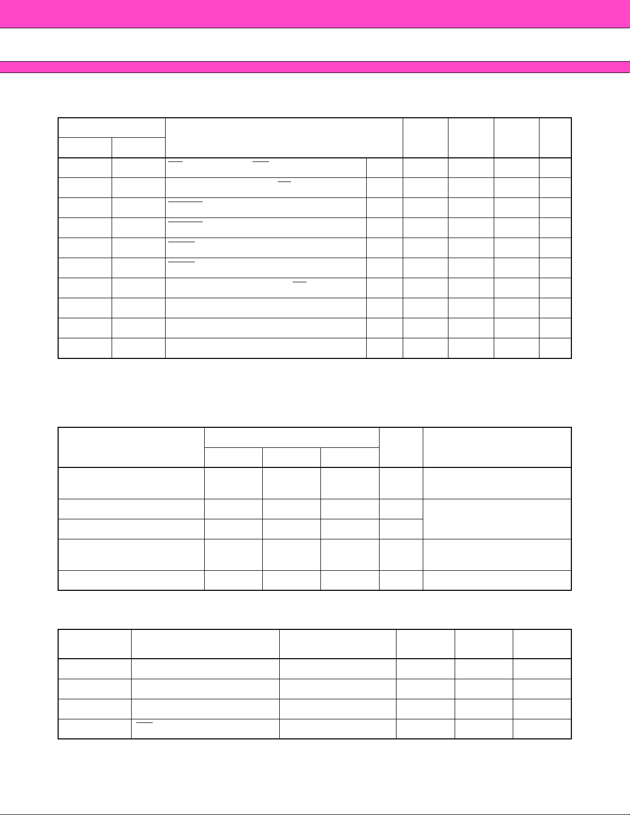
(Continued)
MBM29DL16XTE/BE
-70/90/12
Parameter Symbols
Description 70 90 12 Unit
JEDEC Standard
—t
—t
—t
—t
—t
—t
—t
—t
—t
—t
CSP CE Setup Time to WE Active (Note 2) Min. 4 4 4 µs
RB Recover Time F rom RY/BY Min. 0 0 0 ns
RP RESET Pulse Width Min. 500 500 500 ns
RH RESET High Level Period Before Read Min. 200 200 200 ns
FLQZ BYTE Switching Low to Output High-Z Max. 30 30 40 ns
FHQV BYTE Switching High to Output Active Max. 70 90 120 ns
BUSY Program/Erase Valid to RY/BY Delay Max. 90 90 90 ns
EOE Delay Time from Embedded Output Enable Max. 70 90 120 ns
TOW Erase Time-out Time Min. 50 50 50 µs
SPD Erase Suspend Transition Time Max. 20 20 20 µs
Note: 1.This does not include the preprogramming time.
2.This timing is for Sector Group Protection operation.
ERASE AND PROGRAMMING PERFORMANCE
■
Parameter
Unit Comments
Min. Typ. Max.
Limits
Sector Erase Time — 1 10 s
Word Programming Time — 16 360 µs
Byte Programming Time — 8 300 µs
Chip Programming Time — — 50 s
Excludes programming time
prior to erasure
Excludes system-level
overhead
Excludes system-level
overhead
Program/Erase Cycle 100,000 — — cycle —
PIN CAPACITANCE
■
Parameter
Symbol
C
IN Input Capacitance VIN = 0 6 7.5 pF
OUT Output Capacitance VOUT = 0 8.5 12 pF
C
IN2 Control Pin Capacitance VIN = 0 8 10 pF
C
IN3 WP/ACC Pin Capacitance VIN = 0 17 18 pF
C
Parameter Description Test Setup Typ. Max. Unit
Note: Test conditions TA = 25°C, f = 1.0 MHzs
49
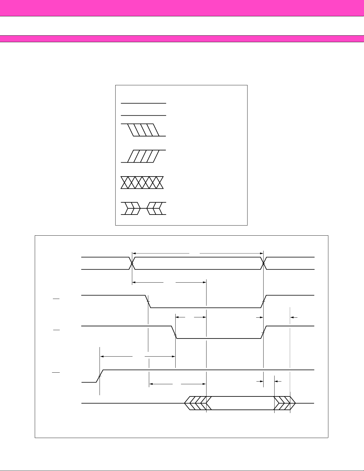
MBM29DL16XTE/BE
TIMING DIAGRAM
■
• Key to Switching Waveforms
WAVEFORM INPUTS OUTPUTS
-70/90/12
Addresses
Must Be
Steady
May
Change
from H to L
May
Change
from L to H
“H” or “L”
Any Change
Permitted
Does Not
Apply
tRC
Addresses Stable
Will Be
Steady
Will Be
Changing
from H to L
Will Be
Changing
from L to H
Changing
State
Unknown
Center Line is
HighImpedance
“Off” State
50
CE
OE
WE
Outputs
tACC
tOE
tOEH
tCE
High-Z
Output Valid
Figure 5.1 AC Waveforms for Read Operations
tOH
t
DF
High-Z
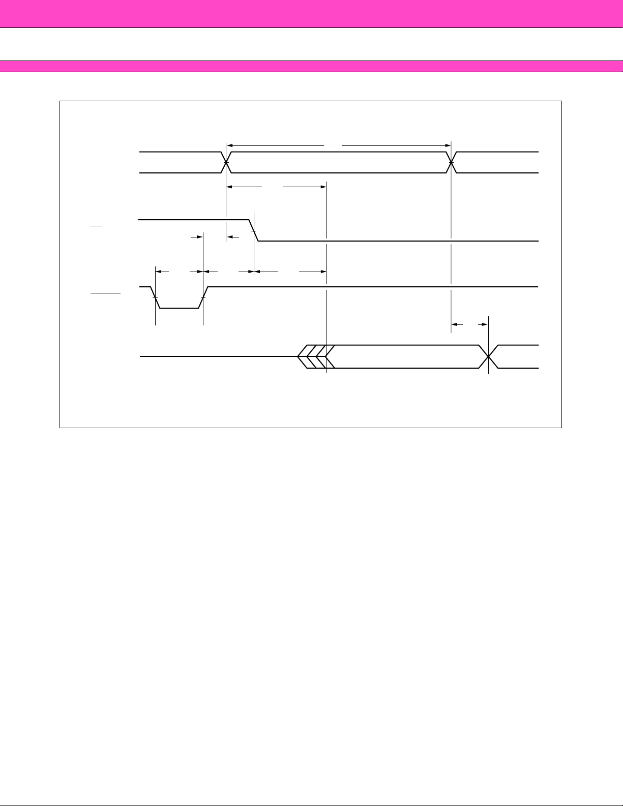
Addresses
tACC
MBM29DL16XTE/BE
tRC
Addresses Stable
-70/90/12
CE
RESET
Outputs
tRH
tRP tRH tCE
tOH
High-Z
Output Valid
Figure 5.2 AC Waveforms for Hardware Reset/Read Operations
51
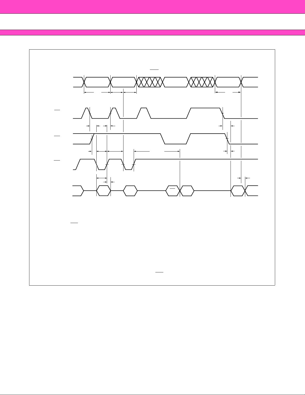
MBM29DL16XTE/BE
-70/90/12
Data Polling
PA
Addresses
3rd Bus Cycle
555H
tWC
tAS
PA
tAH
CE
tCS
tCH
OE
tWP
tGHWL
tWPH
tWHWH1
WE
tDS
tDH
Data
A0H
PD
DQ7
DOUT
Notes: 1. PA is address of the memory location to be programmed.
2. PD is data to be programmed at byte address.
3. DQ
7 is the output of the complement of the data written to the device.
4. DOUT is the output of the data written to the device.
5. Figure indicates last two bus cycles out of four bus cycle sequence.
6. These waveforms are for the ×16 mode. (The addresses differ from ×8 mode.)
tRC
tCE
tOE
tOH
DOUT
52
Figure 6 AC Waveforms for Alternate WE Controlled Program Operations

MBM29DL16XTE/BE
Data Polling3rd Bus Cycle
-70/90/12
Addresses
555H
tWC
PA PA
tAS
tAH
WE
tWS
tWH
OE
tCPH
tGHEL
tCP
tWHWH1
CE
tDS
tDH
Data
A0H
PD
Notes: 1. PA is address of the memory location to be programmed.
2. PD is data to be programmed at byte address.
3. DQ
7 is the output of the complement of the data written to the device.
4. DOUT is the output of the data written to the device.
5. Figure indicates last two bus cycles out of four bus cycle sequence.
6. These waveforms are for the ×16 mode. (The addresses differ from ×8 mode.)
DQ7
OUT
D
Figure 7 AC Waveforms for Alternate CE Controlled Program Operations
53

MBM29DL16XTE/BE
-70/90/12
Addresses*
CE
OE
WE
Data
VCC
1
tGHWL
tVCS
555H
tWC
tCS
tWP
tDS
2AAH 555H
tAS tAH
tCH
tWPH
tDH
555H
2AAH SA*
55H55H 80H AAHAAH
2
10H/
30H
*1:These waveforms are for the ×16 mode. (The addresses differ from ×8 mode.)
*2:SA is the sector address for Sector Erase. Addresses = 555H (Word), AAAH (Byte) for Chip Erase.
Figure 8 AC Waveforms for Chip/Sector Erase Operations
54

CE
MBM29DL16XTE/BE
-70/90/12
tCH
OE
tOEH
WE
tCE
tOE
tDF
*
tEOE
DQ7 =
Valid Data
DQ0 to DQ6
Valid Data
DQ7
DQ0 to DQ6
RY/BY
Data
tWHWH1 or tWHWH2
Data
tBUSY
DQ7
0 to DQ6 = Output Flag
DQ
* :DQ7 = Valid Data (The device has completed the Embedded operation).
Figure 9 AC Waveforms for Data Polling during Embedded Algorithm Operations
High-Z
High-Z
55
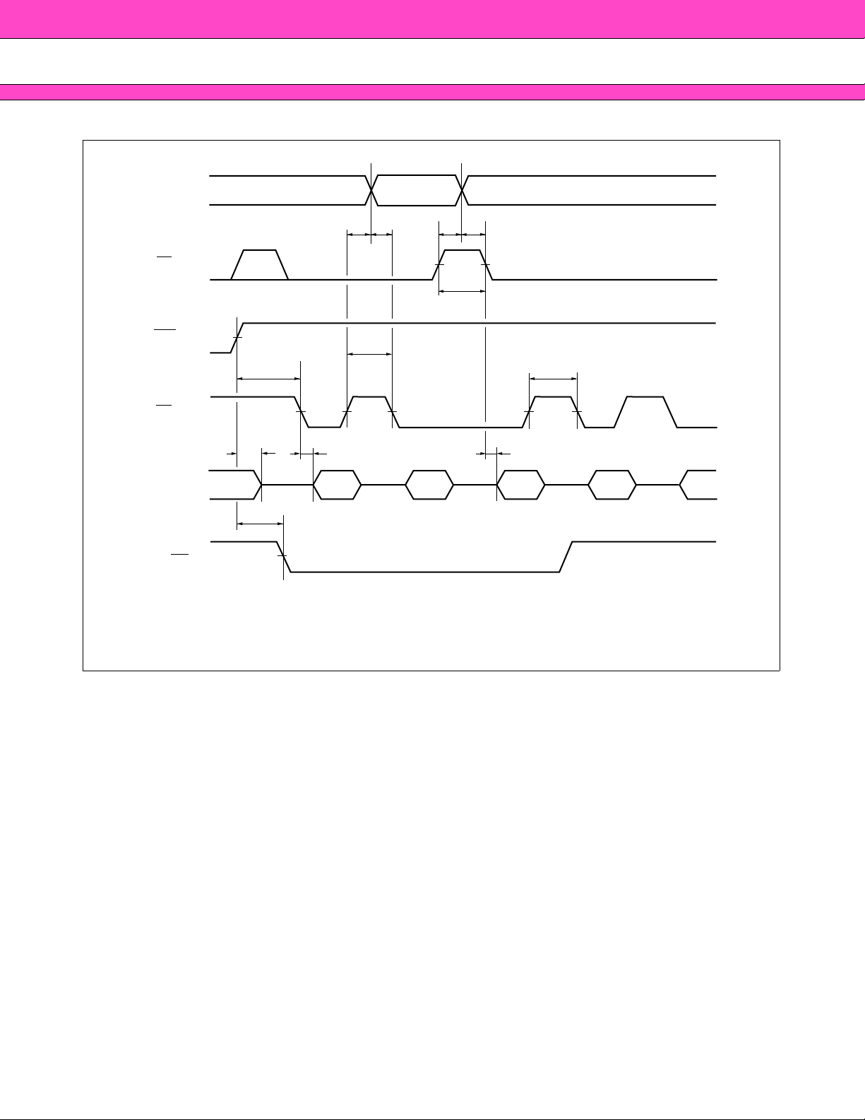
MBM29DL16XTE/BE
Address
tAHT
CE
-70/90/12
tASO
tAHT
tAS
tCEPH
WE
OE
DQ6/DQ2
RY/BY
tOEH
tDH
Data
tBUSY
tOEPH
tOE tCE
Toggle
Data
Toggle
Data
Toggle
Data
tOEH
*
Stop
Toggling
* :DQ6 stops toggling (The device has completed the Embedded operation).
Figure 10 AC Waveforms for Toggle Bit I during Embedded Algorithm Operations
Output
Valid
56
MBM29DL16XTE/BE
Read Command CommandRead Read Read
tRC tRC tRC tRCtWC tWC
-70/90/12
Address BA1 BA1 BA1
tAS
BA2
(555H)
tAH
tACC
tCE
BA2
(PA)
tAHT
tAS
BA2
(PA)
CE
tOE
tCEPH
OE
tGHWL
tWP
tOEH
tDF
WE
tDH
tDS tDF
DQ
Valid
Output
Valid
Intput
Valid
Output
Valid
Intput
Valid
Output
Status
(A0H) (PD)
Note: This is example of Read for Bank 1 and Embedded Algorithm (program) for Bank 2.
BA1: Address of Bank 1.
BA2: Address of Bank 2.
Figure 11 Bank-to-bank Read/Write Timing Diagram
WE
DQ6
DQ2
Enter
Embedded
Erasing
Erase
Suspend
Erase
Toggle
DQ
2 and DQ6
with OE or CE
Erase Suspend
Read
Enter Erase
Suspend Program
Erase
Suspend
Program
Note: DQ2 is read from the erase-suspended sector.
Figure 12 DQ2 vs. DQ
6
Erase Suspend
Read
Erase
Resume
Erase Erase
Complete
57

MBM29DL16XTE/BE
CE
WE
RY/BY
Figure 13 RY/BY Timing Diagram during Program/Erase Operations
-70/90/12
The rising edge of the last write pulse
Entire programming
or erase operations
tBUSY
WE
RESET
RY/BY
tRP
tRB
tREADY
Figure 14 RESET, RY/BY Timing Diagram
58

CE
BYTE
tCE
MBM29DL16XTE/BE
-70/90/12
DQ
DQ
0 to DQ14
0 to DQ14
DQ15/A-1
CE
BYTE
Data Output
(DQ0 to DQ7)
tELFH
tFHQV
A-1
Data Output
(DQ0 to DQ14)
DQ15
Figure 15 Timing Diagram for Word Mode Configuration
tELFL
Data Output
(DQ0 to DQ14)
Data Output
(DQ0 to DQ7)
tACC
DQ15/A-1
DQ15 A-1
tFLQZ
Figure 16 Timing Diagram for Byte Mode Configuration
The falling edge of the last write signal
CE or WE
BYTE
tAS
Input
Valid
tAH
Figure 17 BYTE Timing Diagram for Write Operations
59

MBM29DL16XTE/BE
19, A18, A17
A
A16, A15, A14
A13, A12
A0
A1
A6
VID
3 V
A9
SGAX
tVLHT
-70/90/12
SGAY
VID
3 V
OE
WE
CE
Data
V
CC
tVLHT
tOESP
tCSP
tVCS
SGAX : Sector Group Address for initial sector
SGAY : Sector Group Address for next sector
Note: A-1 is VIL on byte mode.
Figure 18 AC Waveforms for Sector Group Protection
tVLHTtVLHT
tWPP
01H
tOE
60

CC
V
VID
3 V
RESET
CE
WE
tVCS
tVIDR
MBM29DL16XTE/BE
tVLHT
-70/90/12
3 V
RY/BY
tVLHT
Program or Erase Command Sequence
Unprotection period
tVLHT
Figure 19 Temporary Sector Group Unprotection Timing Diagram
61

MBM29DL16XTE/BE
-70/90/12
VCC
RESET
Add SGAXSGAX
A0
1
A
A6
CE
OE
tVIDR
tVCS
tVLHT
tWC tWC
tWP
SGAY
TIME-OUT
WE
Data
60H
60H
SGAX : Sector Group Address to be protected
SGAY : Next Sector Group Address to be protected
TIME-OUT : Time-Out window = 250 µs (min)
Figure 20 Extended Sector Group Protection Timing Diagram
40H
tOE
01H
60H
62

CC
V
VACC
3 V
WP/ACC
CE
WE
tVCS
tVACCR
MBM29DL16XTE/BE
tVLHT
-70/90/12
3 V
RY/BY
tVLHT
Program or Erase Command Sequence
Acceleration period
Figure 21 Accelerated Program Timing Diagram
tVLHT
63
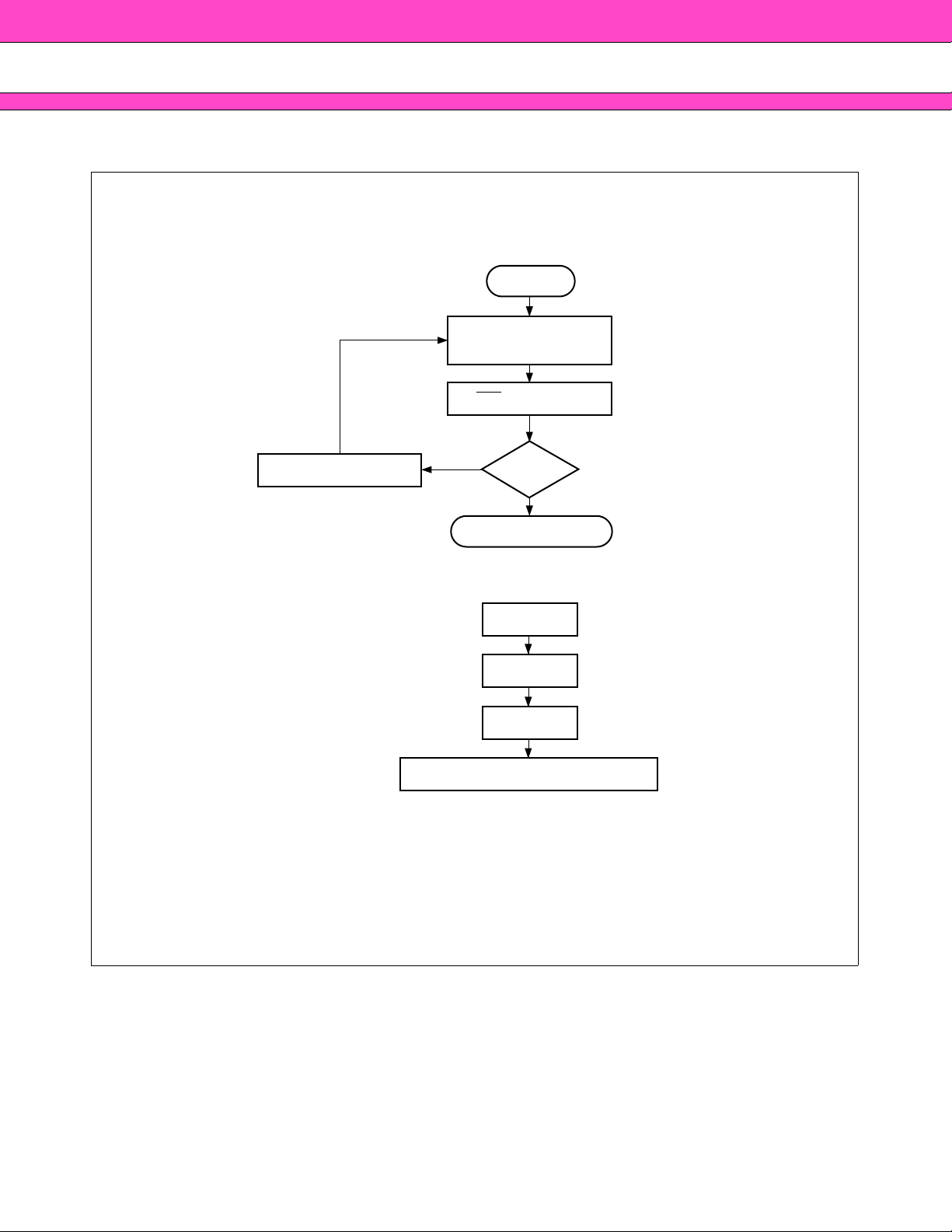
MBM29DL16XTE/BE
FLOW CHART
■
EMBEDDED ALGORITHMS
Increment Address
-70/90/12
Write Program Command
Data Polling Device
No
Start
Sequence
(See below)
Last Address
?
Yes
Program Command Sequence* (Address/Command):
* :The sequence is applied for × 16 mode.
The addresses differ from × 8 mode.
Figure 22 Embedded ProgramTM Algorithm
Programming Completed
555H/AAH
2AAH/55H
555H/A0H
Program Address/Program Data
64
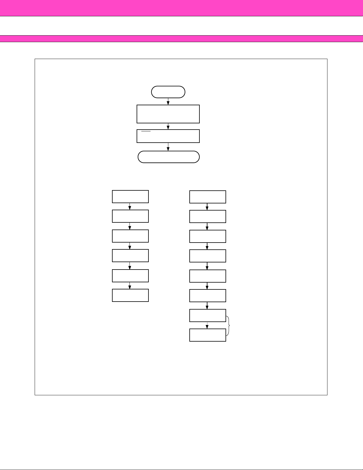
EMBEDDED ALGORITHMS
MBM29DL16XTE/BE
Start
Write Erase Command
Sequence
(See below)
Data Polling or Toggle Bit
Successfully Completed
Erasure Completed
-70/90/12
Chip Erase Command Sequence*
(Address/Command):
555H/AAH
2AAH/55H
555H/80H
555H/AAH
2AAH/55H
555H/10H
Individual Sector/Multiple Sector*
Erase Command Sequence
(Address/Command):
555H/AAH
2AAH/55H
555H/80H
555H/AAH
2AAH/55H
Sector Address/30H
Sector Address/30H
Sector Address/30H
Additional sector
erase commands
are optional.
* :The sequence is applied for × 16 mode.
The addresses differ from × 8 mode.
Figure 23 Embedded EraseTM Algorithm
65

MBM29DL16XTE/BE
(DQ 0 to DQ 7)
Addr. = VA
DQ 7 = Data?
No
DQ 5 = 1?
(DQ 0 to DQ 7)
Addr. = VA
-70/90/12
Start
Read
Yes
No
Yes
Read
VA = Byte address for programming
= Any of the sector addresses within
the sector being erased during
sector erase or multiple sector
erases operation
= Any of the sector addresses within
the sector not being protected
during chip erase
DQ 7 = Data?
Fail
Yes
No
Pass
Note: DQ7 is rechecked even if DQ5 = “1” because DQ7 may change simultaneously with DQ5.
Figure 24 Data Polling Algorithm
66
Start
Read
(DQ
0 to DQ 7)
Addr. = VA
MBM29DL16XTE/BE
VA = Bank address being executed
Embedded Algorithm.
-70/90/12
No
Yes
Yes
No
Yes
Pass
No
DQ 6 = Toggle
?
DQ 5 = 1?
Read
(DQ 0 to DQ 7)
Addr. = VA
DQ 6 = Toggle
?
Fail
Note: DQ6 is rechecked even if DQ5 = “1” because DQ6 may stop toggling at the same time as
DQ
5 changing to “1” .
Figure 25 Toggle Bit Algorithm
67

MBM29DL16XTE/BE
-70/90/12
Start
Setup Sector Group Addr.
(A19, A18, A17, A16, A15, A14, A13, A12)
PLSCNT = 1
=
V ID, A 9
=
=
V ID,
V IH
=
V IH
OE
A
6
= CE =
V IL, RESET
A 0
=
V IL, A 1
Activate WE Pulse
Increment PLSCNT
PLSCNT = 25?
Remove V ID from A 9
Write Reset Command
Device Failed
* :A-1 is V IL on byte mode.
No
Yes
No
Time out 100 µs
WE
=
V IH, CE
= OE =
A 0
Yes
No
=
V IL
V IL
V IL,
)*
(A 9 should remain V ID)
Read from Sector Group
(Addr. = SGA,
A 1
=
V IH
, A 6 =
Data = 01H?
Protect Another Sector
Group ?
Remove V ID from A 9
Write Reset Command
Sector Group Protection
Completed
Yes
68
Figure 26 Sector Group Protection Algorithm
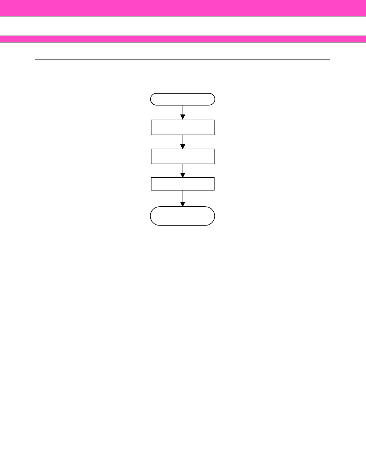
MBM29DL16XTE/BE
Start
RESET = VID
(Note 1)
Perform Erase or
Program Operations
RESET = VIH
-70/90/12
Temporary Sector Group
Unprotection Completed
(Note 2)
Notes: 1. All protected sector groups are unprotected.
2. All previously protected sector groups are protected once again.
Figure 27 Temporary Sector Group Unprotection Algorithm
69
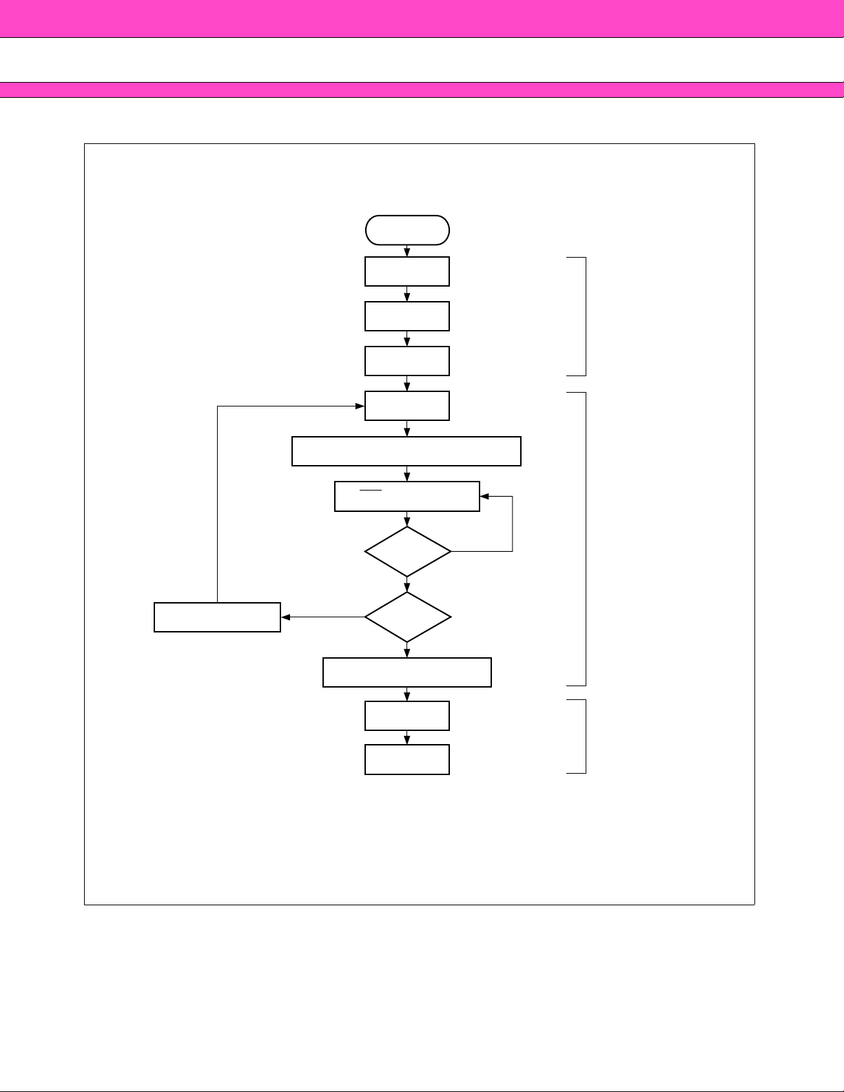
MBM29DL16XTE/BE
FAST MODE ALGORITHM
Program Address/Program Data
-70/90/12
Start
555H/AAH
2AAH/55H Set Fast Mode
555H/20H
XXXH/A0H
Data Polling Device
Verify Byte?
Increment Address
No
Last Address
Programming Completed
(BA)XXXH/90H
XXXH/F0H
Note: The sequence is applied for × 16 mode.
The addresses differ from × 8 mode.
Figure 28 Embedded ProgramTM Algorithm for Fast Mode
No
Yes
?
Yes
In Fast Program
Reset Fast Mode
70
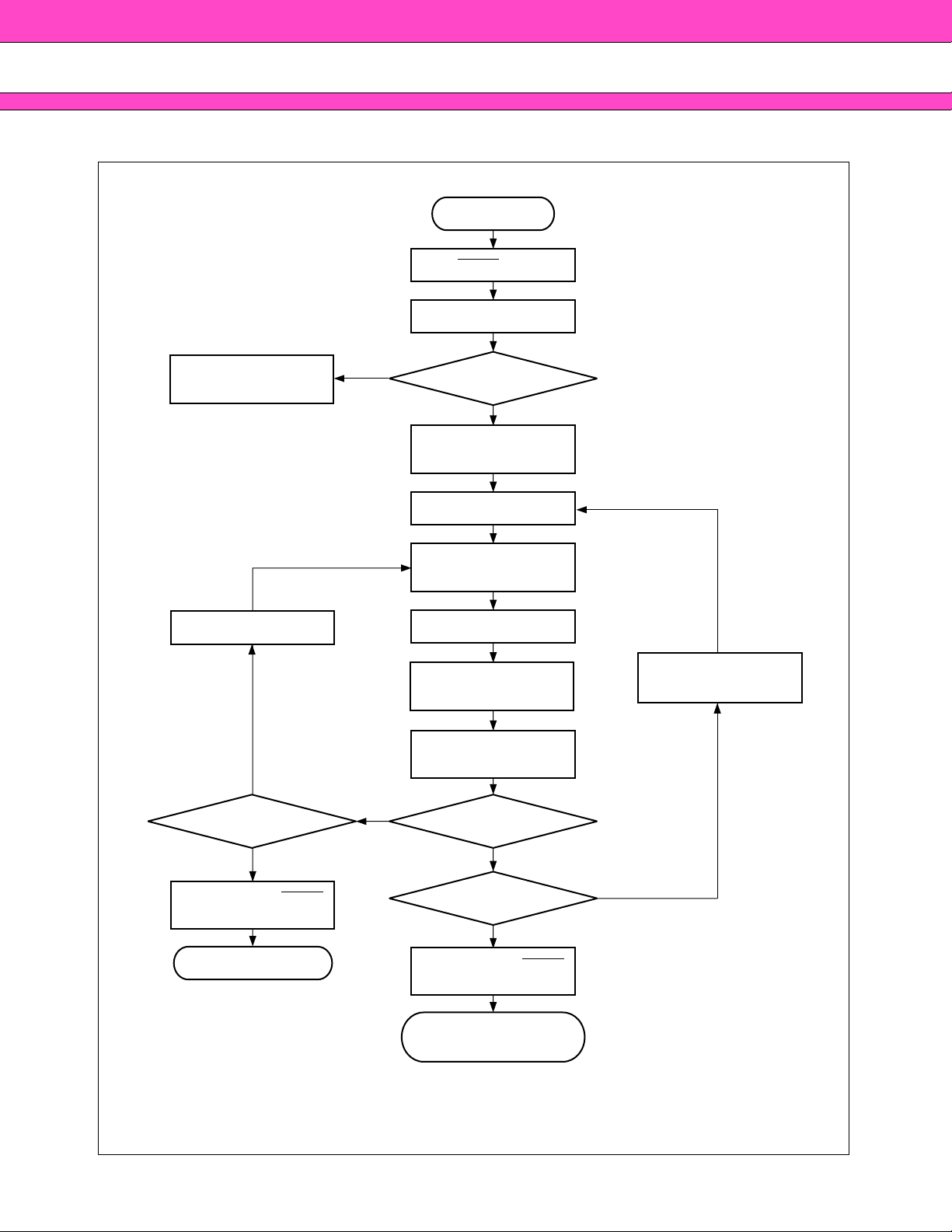
MBM29DL16XTE/BE
Start
RESET = VID
Wait to 4 µs
-70/90/12
Device is Operating in
Temporary Sector Group
Unprotection Mode
Increment PLSCNT
No
PLSCNT = 25
?
No
No
Extended Sector Group
Protection Entry?
Yes
To Setup Sector Group
Protection Write XXXH/60H
PLSCNT = 1
To Sector Group Protection
Write SGA/60H
0 = VIL, A1 = VIH, A6 = VIL)
(A
Time Out 250 µs
To Verify Sector Group
Protection Write SGA/40H
0 = VIL, A1 = VIH, A6 = VIL)
(A
Read from Sector Group
(A
Address
0 = VIL, A1 = VIH, A6 = VIL)
Data = 01H?
Setup Next Sector Group
Address
Yes
Remove V
Write Reset Command
ID from RESET
Device Failed
Figure 29 Extended Sector Group Protection Algorithm
Yes
Protection Other Sector
Group?
No
Remove V
Write Reset Command
Sector Group Protection
ID from RESET
Completed
Yes
71

MBM29DL16XTE/BE
ORDERING INFORMATION
■
-70/90/12
Standard Products
Fujitsu standard products are available in several packages. The order number is formed by a combination of:
MBM29DL16X T E 70 TN
PACKAGE TYPE
TN = 48-Pin Thin Small Outline Package
(TSOP) Standard Pinout
TR = 48-Pin Thin Small Outline Package
(TSOP) Reverse Pinout
PBT = 48-Ball Fine pitch Ball Grid Array
Package (FBGA)
Valid Combinations
MBM29DL161TE/BE
MBM29DL162TE/BE
MBM29DL163TE/BE
MBM29DL164TE/BE
SPEED OPTION
See Product Selector Guide
DEVICE REVISION
BOOT CODE SECTOR ARCHITECTURE
T = To p sector
B = Bottom sector
DEVICE NUMBER/DESCRIPTION
MBM29DL16X
16Mega-bit (2M × 8-Bit or 1M × 16-Bit) CMOS Flash Memory
3.0 V-only Read, Program, and Erase
Valid Combinations
Valid Combinations list configurations planned to
70
90
12
TN
TR
PBT
be supported in volume for this device. Consult
the local Fujitsu sales office to confirm availability
of specific valid combinations and to check on
newly released combinations.
72
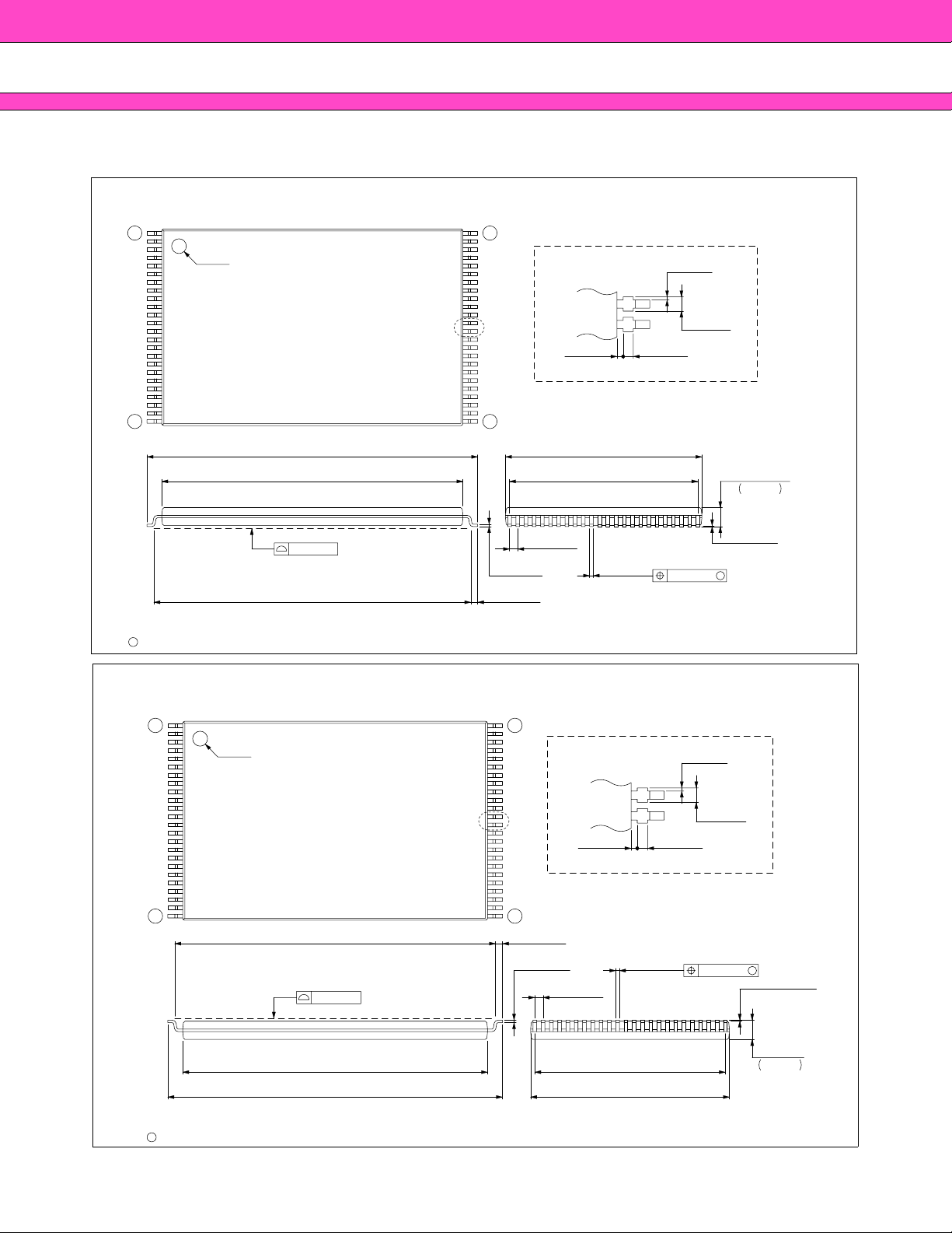
PACKAGE DIMENSIONS
■
MBM29DL16XTE/BE
-70/90/12
48-pin plastic TSOP(I)
(FPT-48P-M19)
LEAD No.
1
INDEX
"A"
24 25
20.00±0.20
(.787±.008)
18.40±0.20
*
(.724±.008)
0.10(.004)
19.00±0.20
(.748±.008)
C
2000 FUJITSU LIMITED F48029S-3c-4
48
0.15±0.05
(.006±.002)
0.50±0.10
(.020±.004)
*: Resin Protrusion. (Each Side: 0.15 (.006) Max)
Details of "A" part
0.15(.006) 0.25(.010)
12.00±0.20
*
(.472±.008)
11.50REF
(.453)
0.50(.0197)
TYP
0.20±0.10
(.008±.004)
0.15(.006)
MAX
0.35(.014)
MAX
+0.10
–0.05
1.10
+.004
.043 –.002
(Mounting height)
0.10±0.05
(.004±.002)
(STAND OFF)
0.10(.004)
M
Dimensions in mm (inches)
48-pin plastic TSOP(I)
(FPT-48P-M20)
LEAD No.
1
INDEX
24 25
19.00±0.20
(.748±.008)
0.10(.004)
18.40±0.20
*
(.724±.008)
20.00±0.20
(.787±.008)
C
2000 FUJITSU LIMITED F48030S-3c-4
"A"
48
0.50±0.10
(.020±.004)
0.15±0.05
(.006±.002)
*: Resin Protrusion. (Each Side: 0.15 (.006) Max)
Details of "A" part
0.15(.006) 0.25(.010)
0.20±0.10
(.008±.004)
0.50(.020)
TYP
11.50(.453)REF
*
12.00±0.20(.472±.008)
0.15(.006)
MAX
0.35(.014)
MAX
0.10(.004)
M
0.10±0.05
(.004±.002)
(STAND OFF)
1.10
.043 –.002
(Mounting height)
Dimensions in mm (inches)
+0.10
–0.05
+.004
(Continued)
73

MBM29DL16XTE/BE
(Continued)
-70/90/12
48-pin plastic FBGA
(BGA-48P-M11)
8.00±0.20(.315±.008)
INDEX
C0.25(.010)
0.10(.004)
6.00±0.20
(.236±.008)
Note: The actual shape of coners may differ from the dimension.
+.006
+0.15
.041 –.004
–0.10
1.05
(Mounting height)
0.38±0.10(.015±.004)
(Stand off)
4.00(.157)
HGFEDCBA
5.60(.221)
0.80(.031)TYP
48-Ø0.45±0.10
(48-.018±.004)
Ø0.08(.003)
6
5
4
3
2
1
M
C
1998 FUJITSU LIMITED B480011S-1C-1
Dimensions in mm (inches)
74

MBM29DL16XTE/BE
FUJITSU LIMITED
For further information please contact:
Japan
FUJITSU LIMITED
Corporate Global Business Support Division
Electronic Devices
KAWASAKI PLANT, 4-1-1, Kamikodanaka,
Nakahara-ku, Kawasaki-shi,
Kanagawa 211-8588, Japan
Tel: +81-44-754-3763
Fax: +81-44-754-3329
http://www.fujitsu.co.jp/
North and South America
FUJITSU MICROELECTRONICS, INC.
3545 North First Street,
San Jose, CA 95134-1804, U.S.A.
Tel: +1-408-922-9000
Fax: +1-408-922-9179
Customer Response Center
Mon. - Fri.: 7 am - 5 pm (PST)
Tel: +1-800-866-8608
Fax: +1-408-922-9179
http://www.fujitsumicro.com/
Europe
FUJITSU MICROELECTRONICS EUR OPE GmbH
Am Siebenstein 6-10,
D-63303 Dreieich-Buchschlag,
Germany
Tel: +49-6103-690-0
Fax: +49-6103-690-122
http://www.fujitsu-fme.com/
Asia Pacific
FUJITSU MICROELECTRONICS ASIA PTE. LTD.
#05-08, 151 Lorong Chuan,
New Tech Park,
Singapore 556741
Tel: +65-281-0770
Fax: +65-281-0220
http://www.fmap.com.sg/
Korea
FUJITSU MICROELECTRONICS K OREA LTD.
1702 KOSMO TOWER, 1002 Daechi-Dong,
Kangnam-Gu,Seoul 135-280
Korea
Tel: +82-2-3484-7100
Fax: +82-2-3484-7111
-70/90/12
All Rights Reserved.
The contents of this document are subject to change without notice.
Customers are advised to consult with FUJITSU sales
representatives before ordering.
The information and circuit diagrams in this document are
presented as examples of semiconductor device applications, and
are not intended to be incorporated in devices for actual use. Also,
FUJITSU is unable to assume responsibility for infringement of
any patent rights or other rights of third parties arising from the use
of this information or circuit diagrams.
The contents of this document may not be reproduced or copied
without the permission of FUJITSU LIMITED.
FUJITSU semiconductor devices are intended for use in standard
applications (computers, office automation and other office
equipments, industrial, communications, and measurement
equipments, personal or household devices, etc.).
CAUTION:
Customers considering the use of our products in special
applications where failure or abnormal operation may directly
affect human lives or cause physical injury or property damage, or
where extremely high levels of reliability are demanded (such as
aerospace systems, atomic energy controls, sea floor repeaters,
vehicle operating controls, medical devices for life support, etc.)
are requested to consult with FUJITSU sales representatives before
such use. The company will not be responsible for damages arising
from such use without prior approval.
Any semiconductor devices have inherently a certain rate of failure.
You must protect against injury, damage or loss from such failures
by incorporating safety design measures into your facility and
equipment such as redundancy, fire protection, and prevention of
over-current levels and other abnormal operating conditions.
If any products described in this document represent goods or
technologies subject to certain restrictions on export under the
Foreign Exchange and Foreign Trade Control Law of Japan, the
prior authorization by Japanese government should be required for
export of those products from Japan.
F0005
FUJITSU LIMITED Printed in Japan

WWW.ALLDATASHEET.COM
Copyright © Each Manufacturing Company.
All Datasheets cannot be modified without permission.
This datasheet has been download from :
www.AllDataSheet.com
100% Free DataSheet Search Site.
Free Download.
No Register.
Fast Search System.
www.AllDataSheet.com
 Loading...