

Page 1

查询MB90341供应商
FUJITSU SEMICONDUCTOR
DATA SHEET
DS07-13730-2E
16-bit Proprietary Microcontroller
CMOS
F2MC-16LX MB90340 Series
MB90F342/C(S), MB90F343/C(S), MB90F345/C(S), MB90F346A(S), MB90F346CA(S),
MB90F347A(S), MB90F347CA(S), MB90F349/C(S), MB90341/C(S), MB90342/C(S), MB90346A(S),
MB90346CA(S), MB90347A(S), MB90347CA(S), MB90348/C(S), MB90349/C(S), MB90V340(S)
DESCRIPTION
■■■■
The MB90340-series with up to 2 FULL-CAN* interfaces and FLASH ROM is especially designed f or automotiv e
and industrial applications. Its main feature are the on-board CAN Interfaces, which conform to V2.0 Part A and
Part B, while supporting a very flexible message buffer scheme and so off ering more functions than a normal full
CAN approach. With the new 0.35 µm CMOS technology, Fujitsu now offers on-chip FLASH-ROM program
memory up to 512 Kbytes.
The power supply (3 V) is supplied to the internal MCU core from an internal regulator circuit. This creates a
major advantage in terms of EMI and power consumption.
The internal PLL clock frequency multiplier provides an internal 42 ns instruction cycle time from an external
4 MHz clock.
The unit features an 8 channel Output Compare Unit and 8 channel Input Capture Unit with 2 separate 16-bit free
running timers. 4 UARTs constitute additional functionality for communication purposes.
* : Controller Area Network (CAN) - License of Robert Bosch GmbH
Note : F
■■■■
2
MC stands for FUJITSU Flexible Microcontroller, a registered trademark of FUJITSU LIMITED.
PACKAGES
100-pin Plastic QFP 100-pin Plastic LQFP
(FPT-100P-M06) (FPT-100P-M05)
Page 2

MB90340 Series
FEATURES
■■■■
••••
Clock
• Built-in PLL clock frequency multiplication circuit
• Selection of machine clocks (PLL clocks) is allow ed among frequency division by two on oscillation cloc k, and
multiplication of 1 to 6 times of oscillation clock (for 4 MHz oscillation clock, 4 MHz to 24 MHz).
• Operation by sub-clock (up to 50 kHz : 100 kHz oscillation clock divided two) is allowed. (devices without Ssuffix only)
• Minimum ex ecution time of instruction : 42 ns (when operating with 4-MHz oscillation clock, and 6-time multiplied PLL clock).
••••
16 Mbyte CPU memory space
• 24-bit internal addressing
••••
Instruction system best suited to controller
• Wide choice of data types (bit, byte, word, and long word)
• Wide choice of addressing modes(23 types)
• Enhanced multiply-divide instructions and RETI instructions
• Enhanced high-precision computing with 32-bit accumulator
••••
Instruction system compatible with high-level language (C language) and multitask
• Employing system stack pointer
• Enhanced various pointer indirect instructions
• Barrel shift instructions
••••
Increased processing speed
• 4-byte instruction queue
••••
Powerful interrupt function
• Powerful 8-level, 34-condition interrupt feature
• Up to 16 external interrupts are supported
••••
Automatic data transfer function independent of CPU
• Expanded intelligent I/O service function (EI
• DMA : up to 16 channels
••••
Low power consumption (standby) mode
• Sleep mode (a mode that halts CPU operating clock)
• Time-base timer mode (a mode that operates oscillation clock, sub clock, time-base timer and cloc k timer only)
• Watch mode (a mode that operates sub clock and clock timer only)
• Stop mode (a mode that stops oscillation clock and sub clock)
• CPU blocking operation mode
••••
Process
•CMOS technology
••••
I/O port
• General-purpose input/output port (CMOS output)
- 80 ports (devices without S-suffix)
- 82 ports (devices with S-suffix)
••••
Timer
• Time-base timer, clock timer, watchdog timer : 1 channel
• 8/16-bit PPG timer : 8-bit X 16 channels, or 16-bit X 8 channels
• 16-bit reload timer : 4 channels
• 16- bit input/output timer
- 16-bit free run timer : 2 channel (FRT0 : ICU 0/1/2/3, OCU 0/1/2/3, FRT1 : ICU 4/5/6/7, OCU 4/5/6/7)
2
OS) : up to 16 channels
2
Page 3

MB90340 Series
- 16- bit input capture: (ICU) : 8 channels
- 16-bit output compare : (OCU) : 8 channels
••••
Full-CAN interface : up to 2 channels
• Compliant with Ver2.0A and Ver2.0B CAN specifications
• Flexible message buffering (mailbox and FIFO buffering can be mixed)
• CAN wake-up function
••••
UART (LIN/SCI) : up to 4 channels
• Equipped with full-duplex double buffer
• Clock-asynchronous or clock-synchronous serial transmission is available
2
••••
I
C interface* : up to 2 channels (devices with C-suffix only)
• Up to 400 kbit/s transfer rate
••••
DTP/External interrupt : up to 16 channels, CAN wakeup : up to 2 channels
• Module for activ ation of expanded intelligent I/O service (EI
••••
Delay interrupt generator module
• Generates interrupt request for task switching.
••••
8/10-bit A/D converter : 16/24 channels
• Resolution is selectable between 8-bit and 10-bit.
• Activation by external trigger input is allowed.
• Conversion time : 3 µs (at 24-MHz machine clock, including sampling time)
2
OS), DMA, and generation of external interrupt.
••••
Program patch function
• Address matching detection for 6 address pointers.
••••
Internal voltage regulator
• Supports 3 V MCU core, offering low EMI and low power consumption figures
••••
Programmable input levels
• Automotive/CMOS-Schmitt (initial level is Automotive in Single chip mode)
• TTL level (initial level for External bus mode)
••••
ROM security function
• Protects the content of ROM (MASK ROM device only)
••••
External bus interface
••••
Clock monitor function
2
* : I
C license :
Purchase of Fujitsu I
ponents in an I
2
C components conveys a license under the Philips I2C Patent Rights to use, these com-
2
C system provided that the system conforms to the I2C Standard Specification as defined by
Philips.
3
Page 4

MB90340 Series
PRODUCT LINEUP
■■■■
Part Number
Parameter
CPU F
System clock
ROM
RAM
Emulator-specific
power supply
*2
Technology
Operating
voltage range
MB90F342/C(S),MB90F343/C(S)*1, MB90F345/C(S), MB90F346A(S),
MB90F346CA(S), MB90F347A(S), MB90F347CA(S), MB90F349/C(S),
MB90341/C(S)*
MB90347A(S), MB90347CA(S), MB90348/C(S)*
1
, MB90342/C(S)*1, MB90346A(S) , MB90346CA(S),
1
, MB90349/C(S)*
2
MC-16LX CPU
1
On-chip PLL clock multiplier (×1, ×2, ×3, ×4, ×6, 1/2 when PLL stops)
Minimum instruction execution time : 42 ns (4 MHz osc. PLL × 6)
Boot-block, Flash memory
512 Kbytes : MB90F345/C (S)
384 Kbytes : MB90F343/C (S)
256 Kbytes : MB90F342/C (S) , MB90F349/C (S) , MB90342/C (S) ,
MB90349/C (S)
128 Kbytes : MB90F347A (S) , MB90F347CA (S) , MB90341/C (S) ,
MB90348/C (S) , MB90347A (S) , MB90347CA (S)
64 Kbytes : MB90F346A (S) , MB90F346CA (S) , MB90346A (S)
MB90346CA (S)
20 Kbytes : MB90F343/C (S) , MB90F345/C (S)
16 Kbytes : MB90F342/C (S) , MB90F349/C (S) , MB90341/C (S) ,
MB90342/C (S) , MB90348/C (S) , MB90349/C (S)
6 Kbytes : MB90F347A (S) , MB90F347CA (S) , MB90347A (S) ,
MB90347CA (S)
2 Kbytes : MB90F346A (S) , MB90F346CA (S) , MB90346A (S) ,
MB90346CA (S)
Yes
0.35 µm CMOS with on-chip voltage regulator for internal
power supply + Flash memory with
On-chip charge pump for programming voltage
3.5 V - 5.5 V : at normal operating (not using A/D converter)
4.0 V - 5.5 V : at using A/D converter/Flash programming
4.5 V - 5.5 V : at using external bus
MB90V340(S)
External
30 Kbytes
0.35 µm CMOS with
on-chip voltage
regulator for internal
power supply
5 V ± 10%
Temperature range −40 °C to +105 °C
Package QFP-100, LQFP-100 PGA-299
4 channels 5 channels
UART
Wide range of baud rate settings using a dedicated reload timer
Special synchronous options for adapting to different synchronous serial protocols
LIN functionality working either as master or slave LIN device
2
C (400 kbit/s)
I
A/D
Converter
devices with ‘C’-suffix : 2ch
devices without ‘C’-suffix :
devices with ‘C’-suffix : 24ch
devices without ‘C’-suffix : 16ch
10-bit or 8-bit resolution
2 channel
24 input channels
Conversion time : Min 3 µs include sample time (per one channel)
1
16-bit Reload Timer
(4 channels)
Operation clock frequency : fsys/2
Supports External Event Count function
, fsys/23, fsys/25 (fsys = Machine clock frequency)
(Continued)
4
Page 5

Part Number
Parameter
16-bit
I/O Timer
(2 channels)
16-bit Output
Compare
(8 channels)
MB90340 Series
MB90F342/C(S),MB90F343/C(S)*1, MB90F345/C(S), MB90F346A(S),
MB90F346CA(S), MB90F347A(S), MB90F347CA(S), MB90F349/C(S),
MB90341/C(S)*
MB90347A(S), MB90347CA(S), MB90348/C(S)*
Signals an interrupt when overflowing
Supports Timer Clear when a match with Output Compare (Channel 0, 4)
Operation clock freq. : fsys, fsys/2
(fsys = Machine clock freq.)
I/O Timer 0 (clock input FRCK0) corresponds to ICU 0/1/2/3, OCU 0/1/2/3
I/O Timer 1 (clock input FRCK1) corresponds to ICU 4/5/6/7, OCU 4/5/6/7
Signals an interrupt when 16-bit I/O Timer match output compare registers.
A pair of compare registers can be used to generate an output signal.
1
, MB90342/C(S)*1, MB90346A(S) , MB90346CA(S),
1
, fsys/22, fsys/23, fsys/24, fsys/25, fsys/26, fsys/2
1
, MB90349/C(S)*
1
MB90V340(S)
7
16-bit Input Capture
(8 channels)
8/16-bit
Programmable Pulse
Generator
(8 channels)
CAN Interface
Rising edge, falling edge or rising & falling edge sensitive
Signals an interrupt upon external event
Supports 8-bit and 16-bit operation modes
Sixteen 8-bit reload counters
Sixteen 8-bit reload registers for L pulse width
Sixteen 8-bit reload registers for H pulse width
A pair of 8-bit reload counters can be configured as one 16-bit reload counter or as
8-bit prescaler plus 8-bit reload counter
Operation clock freq. : fsys, fsys/2
1
, fsys/22, fsys/23, fsys/24 or 128 µs@fosc = 4 MHz
(fsys = Machine clock frequency, fosc = Oscillation clock frequency)
2 channels : MB90F342/C (S) , MB90F343/C (S) , MB90F345/C (S) ,
MB90341/C (S) , MB90342/C (S)
1channel : MB90F346A (S) , MB90F346CA (S) , MB90F347A(S) ,
MB90F347CA (S) , MB90F349/C (S) , MB90346A (S) ,
3 channels
MB90346CA (S) , MB90347A (S) , MB90347CA (S) ,
MB90348/C (S) , MB90349/C (S)
Conforms to CAN Specification Version 2.0 Part A and B
Automatic re-transmission in case of error
Automatic transmission responding to Remote Frame
Prioritized 16 message buffers for data and ID’s
Supports multiple messages
Flexible configuration of acceptance filtering :
Full bit compare/Full bit mask/Two partial bit masks
Supports up to 1 Mbps
External Interrupt
(16 channels)
Can be used rising edge, falling edge, starting up by H/L level input, external interrupt,
expanded inteligent I/O services (EI
2
OS) and DMA
D/A converter 2 channels
Up to100 kHz
Subclock for low
power operation
devices with ‘S’-suffix : with subclock
devices without ‘S’-suffix : without subclock
Virtually all external pins can be used as general purpose I/O port
All push-pull outputs
I/O Ports
Bit-wise settable as input/output or peripheral signal
Settable in pin-wise of 8 as CMOS schmitt trigger/ automotive inputs (default)
TTL input level settable for external bus (32-pin only for external bus)
(Continued)
5
Page 6

MB90340 Series
(Continued)
Part Number
Parameter
Flash
Memory
ROM Security Protects the content of ROM (MASK ROM device only)
*1 : The devices other than MB90F342/C (S) , MB90F345/C (S) , MB90F346A (S) , MB90F346CA (S) ,
MB90F347A (S) , MB90F347CA (S) , MB90F349/C (S) , MB90346A (S) , MB90346CA (S) , MB90347A (S)
and MB90347CA (S) are under development.
MB90F342/C(S),MB90F343/C(S)*1, MB90F345/C(S), MB90F346A(S),
MB90F346CA(S), MB90F347A(S), MB90F347CA(S), MB90F349/C(S),
MB90341/C(S)*
MB90347A(S), MB90347CA(S), MB90348/C(S)*
Supports automatic programming, Embedded Algorithm
1
, MB90342/C(S)*1, MB90346A(S) , MB90346CA(S),
1
, MB90349/C(S)*
TM*3
1
Write/Erase/Erase-Suspend/Resume commands
A flag indicating completion of the algorithm
Number of erase cycles : 10,000 times
Data retention time : 10 years
Boot block configuration
Erase can be performed on each block
Block protection with external programming voltage
Flash Security Feature for protecting the content of the Flash (except for
MB90F346A(S) and MB90F346CA (S) )
MB90V340(S)
*2 : It is setting of Jumper switch (TOOL V
CC) when Emulator (MB2147-01) is used.
Please refer to the Emulator hardware manual about details.
*3 : Embedded Algorithm is a trade mark of Advanced Micro Devices Inc.
6
Page 7

PIN ASSIGNMENTS
■■■■
• MB90V340(S)
MB90340 Series
(TOP VIEW)
P04/AD04/INT12
P05/AD05/INT13
P06/AD06/INT14
P07/AD07/INT15
P10/AD08/TIN1
P11/AD09/TOT1
P12/AD10/SIN3/NT11R
P13/AD11/SOT3
P14/AD12/SCK3
Vcc
Vss
X1
X0
P15/AD13/SIN4
P16/AD14/SOT4
P17/AD15/SCK4
P20/A16/PPG9(8)
P21/A17/PPGB(A)
P22/A18/PPGD(C)
P23/A19/PPGF(E)
P03/AD03/INT11
P02/AD02/INT10
P01/AD01/INT9
P00/AD00/INT8
PA1/TX 0
PA0/RX0/INT8R
P97/OUT3
P96/OUT2
P95/OUT1
P94/OUT0
P93/PPG7(6)
P92/PPG5(4)
P91/PPG3(2)
P90/PPG1(0)
Vss
Vcc
P87/SCK1
P86/SOT1
80 515871 70 67 6669 68 65 64 63 62 6176 75 74 73 72777879 54 535556 5259 5760
81
82
83
84
85
86
87
88
89
90
91
92
93
94
95
96
97
98
99
100
P24/A20/IN0
P25/A21/IN1
P26/A22/IN2
P31/RD/IN5
P27/A23/IN3
P30/ALE/IN4
P33/WRH/TX2
P35/HAK/OUT5
P34/HRQ/OUT4
P36/RDY/OUT6
QFP - 100
P40/X0A*
P37/CLK/OUT7
P41/X1A*
C
Vss
Vcc
P42/IN6/RX1/INT9R
P85/SIN1
P43/IN7/TX1
P84/SCK0/INT15R
21201716 19181514131211 2625242322 27 28 29435629710
P44/SDA0/FRCK0
P83/SOT0/TOT2
P45/SCL0/FRCK1
P82/SIN0/TIN2/INT14R
P46/SDA1
P81/TOT0/CKOT/INT13R
P47/SCL1
P80/TIN0/ADTG/INT12R
RST
P77/AN23/INT7
P76/AN22/INT6
MD0
MD1
MD2
P75/AN21/INT5
50
P74/AN20/INT4
49
P73/AN19/INT3
48
P72/AN18/INT2
47
P71/AN17/INT1
46
P70/AN16/INT0
45
Vss
44
P67/AN7/PPGE(F)
43
P66/AN6/PPGC(D)
42
P65/AN5/PPGA(B)
41
P64/AN4/PPG8(9)
40
P63/AN3/PPG6(7)
39
P62/AN2/PPG4(5)
38
P61/AN1/PPG2(3)
37
P60/AN0/PPG0(1)
36
AVss
35
AVRL
34
AVRH
33
AVcc
32
P57/AN15/DA01
31
3018
P55/AN13
P50/AN8/SIN2
P51/AN9/SOT2
P53/AN11/TIN3
P52/AN10/SCK2
P56/AN14/DA00
P54/AN12/TOT3
* : MB90V340: X0A, X1A
MB90V340S: P40, P41
P32/WRL/WR/RX2/INT10R
(FPT-100P-M06)
(Continued)
7
Page 8

MB90340 Series
(Continued)
P00/AD00/INT8
PA1/T X 0
75
74 73 72 71 70 69 68 67 66 65 64 63 62 61 60 5859 555657 54 53 52 51
76P01/AD01/INT9
77P02/AD02/INT10
78P03/AD03/INT11
Vcc
Vss
X1
X0
79
80
81
82
83
84
85
86
87
88
89
90
91
92
93
94
95
96
97
98
99P24/A20/IN0
100P25/A21/IN1
12345678910111213141516 1817 212019 22 23 24 25
P04/AD04/INT12
P05/AD05/INT13
P06/AD06/INT14
P07/AD07/INT15
P10/AD08/TIN1
P11/AD09/TOT1
P12/AD10/SIN3/NT11R
P13/AD11/SOT3
P14/AD12/SCK3
P15/AD13/SIN4
P16/AD14/SOT4
P17/AD15/SCK4
P20/A16/PPG9(8)
P21/A17/PPGB(A)
P22/A18/PPGD(C)
P23/A19/PPGF(E)
PA0/RX0/INT8R
(TOP VIEW)
P97/OUT3
P96/OUT2
P95/OUT1
P94/OUT0
P93/PPG7(6)
P92/PPG5(4)
P91/PPG3(2)
P90/PPG1(0)
Vss
Vcc
P87/SCK1
P86/SOT1
P85/SIN1
P84/SCK0/INT15R
P83/SOT0/TOT2
P82/SIN0/TIN2/INT14R
P80/TIN0/ADTG/INT12R
P77/AN23/INT7
P76/AN22/INT6
MD0
P81/TOT0/CKOT/INT13R
LQFP - 100
RST
50 MD1
49 MD2
48
47
46
45
44
43
42
41
40
39
38
37
36
35
34
33
32
31
30
29
28
27
26
P75/AN21/INT5
P74/AN20/INT4
P73/AN19/INT3
P72/AN18/INT2
P71/AN17/INT1
P70/AN16/INT0
Vss
P67/AN7/PPGE(F)
P66/AN6/PPGC(D)
P65/AN5/PPGA(B)
P64/AN4/PPG8(9)
P63/AN3/PPG6(7)
P62/AN2/PPG4(5)
P61/AN1/PPG2(3)
P60/AN0/PPG0(1)
AVss
AVRL
AVRH
AVcc
P57/AN15/DA01
P56/AN14/DA00
P55/AN13
P54/AN12/TOT3
C
Vss
Vcc
P45/SCL0/FRCK1
P47/SCL1
P46/SDA1
P50/AN8/SIN2
P51/AN9/SOT2
P53/AN11/TIN3
P52/AN10/SCK2
P41/X1A*
P31/RD/IN5
P26/A22/IN2
P27/A23/IN3
P30/ALE/IN4
P33/WRH/TX2
P35/HAK/OUT5
P34/HRQ/OUT4
P32/WRL/WR/RX2/INT10R
P40/X0A*
P37/CLK/OUT7
P36/RDY/OUT6
P43/IN7/TX1
P44/SDA0/FRCK0
P42/IN6/RX1/INT9R
(FPT-100P-M05)
* : MB90V340 : X0A, X1A
MB90V340S : P40, P41
8
Page 9

MB90340 Series
MB90F342 (S) /MB90F343 (S) /MB90F345 (S) /MB90F346A (S) /MB90F347A (S) /MB90F349 (S) /MB90341 (S) /MB90342 (S) /
•
MB90346A (S) /MB90347A (S) /MB90348 (S) /MB90349 (S)
(TOP VIEW)
P03/AD03/INT11
P02/AD02/INT10
P01/AD01/INT9
P00/AD00/INT8
PA1/T X 0
PA0/RX0/INT8R
P97/OUT3
P96/OUT2
P95/OUT1
P94/OUT0
P93/PPG7(6)
P92/PPG5(4)
P91/PPG3(2)
P90/PPG1(0)
Vss
Vcc
P87/SCK1
P86/SOT1
P85/SIN1
P84/SCK0/INT15R
P83/SOT0/TOT2
P82/SIN0/TIN2/INT14R
P81/TOT0/ CKOT/INT13R
P80/TIN0/ADTG/INT12R
P77/INT7
P76/INT6
MD0
MD1
MD2
RST
P04/AD04/INT12
P05/AD05/INT13
P06/AD06/INT14
P07/AD07/INT15
P10/AD08/TIN1
P11/AD09/TOT1
P12/AD10/SIN3/NT11R
P13/AD11/SOT3
P14/AD12/SCK3
Vcc
Vss
X1
X0
P15/AD13
P16/AD14
P17/AD15
P20/A16/PPG9(8)
P21/A17/PPGB(A)
P22/A18/PPGD(C)
P23/A19/PPGF(E)
80 79 78 77 76 75 74 73 72 71 70 69 68 67 66 65 64 63 62 61 60 59 58 57 56 55 54 53 52 51
81
82
83
84
85
86
87
88
89
90
91
92
93
94
95
96
97
98
99
100
1 2 3 4 5 6 7 8 9 101112131415161718192021222324252627282930
P33/WRH
P24/A20/IN0
P25/A21/IN1
P26/A22/IN2
P31/RD/IN5
P27/A23/IN3
P30/ALE/IN4
P32/WRLX/WRX/INT10R
P35/HAK/OUT5
P34/HRQ/OUT4
P37/CLK/OUT7
P36/RDY/OUT6
QFP - 100
Vss
Vcc
P41/X1A *
P40/X0A *
C
P44/FRCK0
P43/IN7/TX1
P42/IN6/RX1/INT9R
P46
P45/FRCK1
P47
P50/AN8/SIN2
P51/AN9/SOT2
P53/AN11/TIN3
P52/AN10/SCK2
(FPT-100P-M06)
P75/INT5
50
P74/INT4
49
P73/INT3
48
P72/INT2
47
P71/INT1
46
P70/INT0
45
44
Vss
43
P67/AN7/PPGE(F)
42
P66/AN6/PPGC(D)
41
P65/AN5/PPGA(B)
40
P64/AN4/PPG8(9)
39
P63/AN3/PPG6(7)
38
P62/AN2/PPG4(5)
37
P61/AN1/PPG2(3)
36
P60/AN0/PPG0(1)
35
AVss
34
AVRL
33
AVRH
32
AVcc
31
P57/AN15
P56/AN14
P55/AN13
P54/AN12/TOT3
* : MB90F342/F343/F345/F346A/F347A/F349/341/342/346A/347A/348/349 : X0A, X1A
MB90F342S/F343S/F345S/F346AS/F347AS/F349S/341S/342S/346AS/347AS/348S/349S : P40,P41
(Continued)
9
Page 10

MB90340 Series
(Continued)
P00/AD00/INT8
PA1/TX 0
75 74 73 72 71 70 69 68 67 66 65 64 63 62 61 60 59 58 57 56 55 54 53 52 51
Vcc
Vss
X1
X0
76
77
78
79
80
81
82
83
84
85
86
87
88
89
90
91
92
93
94
95
96
97
98
99
100
12345678910111213141516171819202122232425
P01/AD01/INT9
P02/AD02/INT10
P03/AD03/INT11
P04/AD04/INT12
P05/AD05/INT13
P06/AD06/INT14
P07/AD07/INT15
P10/AD08/TIN1
P11/AD09/TOT1
P12/AD10/SIN3/NT11R
P13/AD11/SOT3
P14/AD12/SCK3
P15/AD13
P16/AD14
P17/AD15
P20/A16/PPG9(8)
P21/A17/PPGB(A)
P22/A18/PPGD(C)
P23/A19/PPGF(E)
P24/A20/IN0
P25/A21/IN1
(TOP VIEW)
PA0/RX0/INT 8R
P97/OUT3
P96/OUT2
P95/OUT1
P94/OUT0
P93/PPG7(6)
P92/PPG5(4)
P91/PPG3(2)
P90/PPG1(0)
Vss
Vcc
P87/SCK1
P86/SOT1
P85/SIN1
P84/SCK0/INT15R
P83/SOT0/TOT2
P82/SIN0/TIN2/INT14R
P80/TIN0/ADTG/INT1 2 R
P77/INT7
P76/INT6
P81/TOT0/CKOT/INT13R
LQFP - 100
MD0
RST
50 MD1
49
48
47
46
45
44
43
42
41
40
39
38
37
36
35
34
33
32
31
30
29
28
27
26
MD2
P75/INT5
P74/INT4
P73/INT3
P72/INT2
P71/INT1
P70/INT0
Vss
P67/AN7/PPGE(F)
P66/AN6/PPGC(D)
P65/AN5/PPGA(B)
P64/AN4/PPG8(9)
P63/AN3/PPG6(7)
P62/AN2/PPG4(5)
P61/AN1/PPG2(3)
P60/AN0/PPG0(1)
AVss
AVRL
AVRH
AVcc
P57/AN15
P56/AN14
P55/AN13
P54/AN12/TOT3
10
C
Vss
P26/A22/IN2
P27/A23/IN3
Vcc
P30/ALE/IN4
P32/WRL/WR/INT10R
P35/HAK/OUT5
P34/HRQ/OUT4
P36/RDY/OUT6
P33/WRH
P31/RD/IN5
P41/X1A*
P40/X0A*
P37/CLK/OUT7
P42/IN6/RX1/INT9R
P44/FRCK0
P43/IN7/TX1
P47
P46
P45/FRCK1
P50/AN8/SIN2
P51/AN9/SOT2
P53/AN11/TIN3
P52/AN10/SCK2
(FPT-100P-M05)
* : MB90F342/F343/F345/F346A/F347A/F349/341/342/346A/347A/348/349 : X0A, X1A
MB90F342S/F343S/F345S/F346AS/F347AS/F349S/341S/342S/346AS/347AS/348S/349S : P40,P41
Page 11

MB90340 Series
• MB90F342C (S) /MB90F343C (S) /MB90F345C (S) /MB90F346CA (S) /MB90F347CA (S) /MB90F349C (S) /
MB90341C (S) /MB90342C (S) /MB90346CA (S) /MB90347CA (S) /MB90348C (S) /MB90349C (S)
(TOP VIEW)
P05/AD05/INT13
P06/AD06/INT14
P07/AD07/INT15
P10/AD08/TIN1
P11/AD09/TOT1
P12/AD10/SIN3/NT11R
P13/AD11/SOT3
P14/AD12/SCK3
Vcc
Vss
X1
X0
P15/AD1 3
P16/AD1 4
P17/AD1 5
P20/A16/PPG9(8)
P21/A17/PPGB(A)
P22/A18/PPGD(C)
P23/A19/PPGF(E)
P03/AD03/INT11
P02/AD02/INT10
P01/AD01/INT9
P00/AD00/INT8
PA1/T X 0
PA0/RX0/INT 8R
P97/OUT3
P96/OUT2
P95/OUT1
P94/OUT0
P93/PPG7(6)
P92/PPG5(4)
P91/PPG3(2)
P90/PPG1(0)
Vss
Vcc
P87/SCK1
P86/SOT1
P85/SIN1
P84/SCK0/INT15R
P83/SOT0/TOT2
P82/SIN0/TIN2/INT14R
P81/TOT0/ CKOT/INT13R
P80/TIN0/ADTG/INT12R
80 79 78 77 76 75 74 73 72 71 70 69 68 67 66 65 64 63 62 61 60 59 58 57 56 55 54 53 52 51
81
82
83
84
85
86
87
88
89
90
91
92
93
94
95
96
97
98
99
100
123456789101112131415161718192021222324252627282930
P33/WRH
P24/A20/IN0
P25/A21/IN1
P26/A22/IN2
P31/RD/IN5
P27/A23/IN3
P30/ALE/IN4
P34/HRQ/OUT4
P32/WRL/WR/INT10R
P35/HAK/OUT5
P37/CLK/OUT7
P36/RDY/OUT6
QFP - 100
Vss
Vcc
P41/X1A*
P40/X0A*
C
P47/SCL1
P45/SCL0/FRCK1
P44/SDA0/FRCK0
P46/SDA1
P50/AN8/SIN2
P43/IN7/TX1
P42/IN6/RX1/INT9R
P77/AN23/INT7
RST
P76/AN22/INT6
MD0
P53/AN11/TIN3
P51/AN9/SOT2
P54/AN12/TOT3
P52/AN10/SCK2
MD1
MD2
P75/AN21/INT5
50P04/AD04/INT12
P74/AN20/INT4
49
P73/AN19/INT3
48
P72/AN18/INT2
47
P71/AN17/INT1
46
P70/AN16/INT0
45
Vss
44
P67/AN7/PPGE(F)
43
P66/AN6/PPGC(D)
42
P65/AN5/PPGA(B)
41
P64/AN4/PPG8(9)
40
P63/AN3/PPG6(7)
39
P62/AN2/PPG4(5)
38
P61/AN1/PPG2(3)
37
P60/AN0/PPG0(1)
36
AVss
35
AVRL
34
AVRH
33
AVcc
32
P57/AN15
31
P56/AN14
P55/AN13
FPT-100P-M06
(
)
* : MB90F342C/F343C/F345C/F346CA/F347CA/F349C/341C/342C/346CA/347CA/348C/349C : X0A, X1A
MB90F342CS/F343CS/F345CS/F346CAS/F347CAS/F349CS/341CS/342CS/346CAS/347CAS/348CS/349CS : P40, P41
(Continued)
11
Page 12

MB90340 Series
(Continued)
(TOP VIEW)
P04/AD04/INT12
P05/AD05/INT13
P06/AD06/INT14
P07/AD07/INT15
P10/AD08/TIN1
P11/AD09/TOT1
P12/AD10/SIN3/NT11R
P13/AD11/SOT3
P14/AD12/SCK3
Vcc
Vss
X1
X0
P15/AD13
P16/AD14
P17/AD15
P20/A16/PPG9(8)
P21/A17/PPGB(A)
P22/A18/PPGD(C)
P23/A19/PPGF(E)
P00/AD00/INT8
PA1/TX 0
PA0/RX0/INT 8R
P97/OUT3
P96/OUT2
P95/OUT1
P94/OUT0
P93/PPG7(6)
P92/PPG5(4)
P91/PPG3(2)
P90/PPG1(0)
Vss
Vcc
P87/SCK1
P86/SOT1
P85/SIN1
P84/SCK0/INT15R
P83/SOT0/TOT2
P82/SIN0/TIN2/INT14R
P80/TIN0/ADTG/INT1 2R
P77/AN23/INT7
P81/TOT0/CKOT/INT13R
75 74 73 72 71 70 69 68 67 66 65 64 63 62 61 60 59 58 57 56 55 54 53 52 51
76P01/AD01/INT9
77P02/AD02/INT10
78P03/AD03/INT11
79
80
81
82
83
84
85
86
87
88
89
90
91
92
93
94
95
96
97
98
99P24/A20/IN0
100P25/A21/IN1
12345678910111213141516171819202122232425
LQFP - 100
P76/AN22/INT6
RST
MD0
50 MD1
49
48
47
46
45
44
43
42
41
40
39
38
37
36
35
34
33
32
31
30
29
28
27
26
MD2
P75/AN21/INT5
P74/AN20/INT4
P73/AN19/INT3
P72/AN18/INT2
P71/AN17/INT1
P70/AN16/INT0
Vss
P67/AN7/PPGE(F)
P66/AN6/PPGC(D)
P65/AN5/PPGA(B)
P64/AN4/PPG8(9)
P63/AN3/PPG6(7)
P62/AN2/PPG4(5)
P61/AN1/PPG2(3)
P60/AN0/PPG0(1)
AVss
AVRL
AVRH
AVcc
P57/AN15
P56/AN14
P55/AN13
P54/AN12/TOT3
C
Vss
Vcc
P41/X1A*
P26/A22/IN2
P27/A23/IN3
P30/ALE/IN4
P32/WRL/WR/INT10R
P35/HAK/OUT5
P34/HRQ/OUT4
P33/WRH
P31/RD/IN5
P40/X0A*
P37/CLK/OUT7
P36/RDY/OUT6
P42/IN6/RX1/INT9R
P43/IN7/TX1
P44/SDA0/FRCK0
P46/SDA1
P45/SCL0/FRCK1
P47/SCL1
P50/AN8/SIN2
P51/AN9/SOT2
P53/AN11/TIN3
P52/AN10/SCK2
(FPT-100P-M05)
* : MB90F342C/F343C/F345C/F346CA/F347CA/F349C/341C/342C/346CA/347CA/348C/349C : X0A, X1A
MB90F342CS/F343CS/F345CS/F346CAS/F347CAS/F349CS/341CS/342CS/346CAS/347CAS/348CS/349CS : P40, P41
12
Page 13

PIN DESCRIPTION
■■■■
MB90340 Series
Pin No.
LQFP100*
75 to 82 77 to 84
2
QFP100*
90 92 X1
91 93 X0 Oscillation input
52 54 RST
83 85
84 86
85 87
86 88
87 89
Pin name
1
P00 to P07
AD00 to AD07
INT8 to INT15 External interrupt request input pins for INT8 to INT15.
P10
AD08
TIN1 Event input pin for the reload timer 1
P11
AD09
TOT1 Output pin for the reload timer 1
P12
AD10
SIN3 Serial data input pin for UART3
INT11R Sub external interrupt request input pin for INT11
P13
AD11
SOT3 Serial data output pin for UART3
P14
AD12
SCK3 Clock I/O pin for UART3
Circuit
type
Oscillation output
A
E Reset input
General purpose I/O. The register can be set to select whether
to use a pull-up resistor. This function is enabled in single-chip
mode.
G
I/O pins for 8 lower bits of the external address/data bus.
This function is enabled when the external bus is enabled.
General purpose I/O. The register can be set to select whether
to use a pull-up resistor. This function is enabled in single-chip
mode.
G
I/O pin for 8th bit of the external address/data bus.
This function is enabled when the external bus is enabled.
General purpose I/O. The register can be set to select whether
to use a pull-up resistor. This function is enabled in single-chip
mode.
G
I/O pin for 9th bit of the external address/data bus.
This function is enabled when the external bus is enabled.
General purpose I/O. The register can be set to select whether
to use a pull-up resistor. This function is enabled in single-chip
mode.
I/O pin for 10th bit of the external address/data bus.
N
This function is enabled when the external bus is enabled.
General purpose I/O. The register can be set to select whether
to use a pull-up resistor. This function is enabled in single-chip
mode.
G
I/O pin for 11th bit of the external address/data bus.
This function is enabled when the external bus is enabled.
General purpose I/O. The register can be set to select whether
to use a pull-up resistor. This function is enabled in single-chip
mode.
G
I/O pin for 12th bit of the external address/data bus.
This function is enabled when the external bus is enabled.
Function
(Continued)
13
Page 14

MB90340 Series
Pin No.
LQFP100
95 to 98 97 to 100
99 to 2 1 to 4
*2
QFP100
92 94
93 95
94 96
35
Pin name
*1
P15
AD13
SIN4 Serial data input pin for UART4 (MB90V340 only)
P16
AD14
SOT4 Serial data output pin for UART4 (MB90V340 only)
P17
AD15
SCK4 Clock I/O pin for UART4 (MB90V340 only)
P20 to P23
A16 to A19
PPG9,PPGB,
PPGD,PPGF
P24 to P27
A20 to A23
IN0 to IN3 Data sample input pins for input captures ICU0 to ICU3
P30
ALE
IN4 Data sample input pin for input capture ICU4
Circuit
type
G
G
G
G
G
G
Function
General purpose I/O. The register can be set to select whether
to use a pull-up resistor. This function is enabled in single-chip
mode.
I/O pin for 13th bit of the external address/data bus.
This function is enabled when the external bus is enabled.
General purpose I/O. The register can be set to select whether
to use a pull-up resistor. This function is enabled in single-chip
mode.
I/O pin for 14th bit of the external address/data bus.
This function is enabled when the external bus is enabled.
General purpose I/O. The register can be set to select whether
to use a pull-up resistor. This function is enabled in single-chip
mode.
I/O pin for 15th bit of the external address/data bus. This function is enabled when the external bus is enabled.
General purpose I/O. The register can be set to select whether
to use a pull-up resistor.In external bus mode, the pin is
enabled as a general-purpose I/O port when the corresponding
bit in the external address output control register (HACR) is 1.
Output pins for A16 to A19 of the external address bus. When
the corresponding bit in the external address output control
register (HACR) is 0, the pins are enabled as high address
output pins (A16 to A19).
Output pins for PPGs
General purpose I/O. The register can be set to select whether
to use a pull-up resistor.In external bus mode, the pin is
enabled as a general-purpose I/O port when the corresponding
bit in the external address output control register (HACR) is 1.
Output pins for A20 to A23 of the external address bus. When
the corresponding bit in the external address output control
register (HACR) is 0, the pins are enabled as high address
output pins (A20 to A23).
General purpose I/O.The register can be set to select whether
to use a pull-up resistor.This function is enabled in single-chip
mode.
Address latch enable output pin. This function is enabled when
the external bus is enabled.
(Continued)
14
Page 15

MB90340 Series
Pin No.
LQFP100
*2
QFP100
46
57
68
79
810
911
Pin name
*1
P31
RD
IN5 Data sample input pin for input capture ICU5
P32
/ WR
WRL
RX2 RX input pin for CAN2 Interface (MB90V340 only)
INT10R Sub external interrupt request input pin for INT10
P33
WRH
TX2 TX Output pin for CAN2 (MB90V340 only)
P34
HRQ
OUT4 Waveform output pin for output compare OCU4
P35
HAK
OUT5 Waveform output pin for output compare OCU6
P36
RDY
OUT6 Waveform output pin for output compare OCU5
Circuit
type
G
G
G
G
G
G
General purpose I/O.The register can be set to select whether to
use a pull-up resistor.This function is enabled in single-chip
mode.
Read strobe output pin for the data bus. This function is enabled
when the external bus is enabled.
General purpose I/O. The register can be set to select whether to
use a pull-up resistor. This function is enabled either in single-chip
mode or with the WR
Write strobe output pin for the data bus. This function is enabled
when both the external bus and the WR
abled. WRL
16-bit access while WR
bus in 8-bit access.
General purpose I/O. The register can be set to select whether to
use a pull-up resistor.This function is enabled either in single-chip
mode or with the WRH
Write strobe output pin for the 8 higher bits of the data bus. This
function is enabled when the external bus is enabled, when the
external bus 16-bit mode is selected, and when the WRH output
pin is enabled.
General purpose I/O. The register can be set to select whether to
use a pull-up resistor. This function is enabled either in single-chip
mode or with the hold function disabled.
Hold request input pin. This function is enabled when both the external bus and the hold function are enabled.
General purpose I/O. The register can be set to select whether to
use a pull-up resistor. This function is enabled either in single-chip
mode or with the hold function disabled.
Hold acknowledge output pin. This function is enabled when both
the external bus and the hold function are enabled.
General purpose I/O. The register can be set to select whether to
use a pull-up resistor. This function is enabled either in single-chip
mode or with the external ready function disabled.
Ready input pin. This function is enabled when both the
external bus and the external ready function are enabled.
is used to write-strobe 8 lower bits of the data bus in
Function
/WRL pin output disabled.
is used to write-strobe 8 bits of the data
pin output disabled.
/WRL pin output are en-
(Continued)
15
Page 16

MB90340 Series
Pin No.
LQFP100
*2
QFP100
10 12
11 to 12 13 to 14
16 18
17 19
18 20
19 21
20 22
21 23
22 24
23 25
24 26
25 27
*1
Pin name
Circuit
type
Function
General purpose I/O. The register can be set to select whether
P37
to use a pull-up resistor. This function is enabled either in
single-chip mode or with the CLK output disabled.
G
CLK
CLK output pin. This function is enabled when both the
external bus and CLK output are enabled.
OUT7 Waveform output pin for output compare OCU7
P40 to P41 F General purpose I/O (devices with S-suffix)
X0A , X1A B Oscillator input pins for sub-clock (devices without S-suffix)
P42
General purpose I/O
IN6 Data sample input pin for input capture ICU6
F
RX1
RX input pin for CAN1 Interface
(MB90F342/F343/F345/341/342 only)
INT9R Sub external interrupt request input pin for INT10
P43
IN7 Data sample input pin for input capture ICU7
General purpose I/O
F
TX1 TX Output pin for CAN1 (MB90F342/F343/F345/341/342 only)
P44
SDA0 Serial data I/O pin for I2C 0 (devices with C-suffix)
General purpose I/O
H
FRCK0 Input for the 16-bit I/O Timer 0
P45
SCL0 Serial clock I/O pin for I2C 0 (devices with C-suffix)
General purpose I/O
H
FRCK1 Input for the 16-bit I/O Timer 1
P46
General purpose I/O
H
SDA1 Serial data I/O pin for I2C 1 (devices with C-suffix)
P47
SCL1 Serial clock I/O pin for I
P50
AN8 Analog input pin for the A/D converter
General purpose I/O
H
General purpose I/O
O
2
C 1 (devices with C-suffix)
SIN2 Serial data input pin for UART2
P51
AN9 Analog input pin for the A/D converter
General purpose I/O
I
SOT2 Serial data output pin for UART2
P52
AN10 Analog input pin for the A/D converter
General purpose I/O
I
SCK2 Clock I/O pin for UART2
P53
AN11 Analog input pin for the A/D converter
General purpose I/O
I
TIN3 Event input pin for the reload timers 3
(Continued)
16
Page 17

MB90340 Series
Pin No.
LQFP100
28, 29 30, 31
34 to 41 36 to 43
43 to 48,
53, 54
*2
QFP100
26 28
27 29
45 to 50,
55, 56
55 57
56 58
57 59
58 60
59 61
60 62
61 63
Pin name
*1
P54
AN12 Analog input pin for the A/D converter
TOT3 Output pin for the reload timer 3
P55
AN13 Analog input pin for the A/D converter
P56 to P57
AN14 to AN15 Analog input pin for the A/D converter
DA00 to DA01 D/A converter analog output pins (MB90V340 only)
P60 to P67
AN0 to AN7 Analog input pins for the A/D converter
PPG0, 2, 4, 6,
8, A, C, E
P70 to P77
AN16 to AN23 Analog input pins for the A/D converter (devices with C-suffix)
INT0 to INT7 External interrupt request input pins for INT0 to INT7
P80
TIN0 Event input pin for the reload timers 0
ADTG Trigger input pin for the A/D converter
INT12R Sub external interrupt request input pin for INT12
P81
TOT0 Output pin for the reload timer 0
CKOT Output pin for the clock monitor
INT13R Sub external interrupt request input pin for INT13
P82
SIN0 Serial data input pin for UART0
TIN2 Event input pin for the reload timers 2
INT14R Sub external interrupt request input pin for INT14
P83
SOT0 Serial data output pin for UART0
TOT2 Output pin for the reload timer 2
P84
SCK0 Clock I/O pin for UART0
INT15R Sub external interrupt request input pin for INT15
P85
SIN1 Serial data input pin for UART1
P86
SOT1 Serial data output pin for UART1
Circuit
type
I
I
J
I
I
F
F
M
F
F
M
F
General purpose I/O
General purpose I/O
General purpose I/O
General purpose I/O
Output pins for PPGs
General purpose I/O
General purpose I/O
General purpose I/O
General purpose I/O
General purpose I/O
General purpose I/O
General purpose I/O
General purpose I/O
Function
(Continued)
17
Page 18

MB90340 Series
(Continued)
Pin No.
LQFP100
*2
QFP100
*1
Pin name
P87
62 64
SCK1 Clock I/O pin for UART1
P90 to P93
65 to 68 67 to 70
PPG1, 3, 5, 7 Output pins for PPGs
P94 to P97
69 to 72 71 to 74
OUT0 to
OUT3
PA0
73 75
RX0 RX input pin for CAN0 Interface
INT8R Sub external interrupt request input pin for INT8
PA1
74 76
TX0 TX Output pin for CAN0
30 32 AV
CC K Vcc power input pin for analog circuits
31 33 AVRH L
32 34 AVRL K Lower reference voltage input for the A/D Converter
33 35 AV
SS K Vss power input pin for analog circuits
50, 51 52, 53 MD1, MD0 C
49 51 MD2 D
13
63
88
14
42
64
89
15
65
90
16
44
66
91
CC Power (3.5 V to 5.5 V) input pins
V
SS Power (0V) input pins
V
15 17 C K
Circuit
type
F
F
F
F
F
Function
General purpose I/O
General purpose I/O
General purpose I/O
Waveform output pins for output compares OCU0 to OCU3.
This function is enabled when the OCU enables waveform
output.
General purpose I/O
General purpose I/O
Reference voltage input for the A/D Converter. This power
supply must be turned on or off while a voltage higher than or
equal to AVRH is applied to AV
CC.
Input pins for specifying the operating mode. The pins must be
directly connected to Vcc or Vss
Input pin for specifying the operating mode. The pins must be
directly connected to Vcc or Vss.
This is the power supply stabilization capacitor pin. It should be
connected to a higher than or equal to 0.1 µF ceramic capacitor.
*1 : FPT-100P-M06
*2 : FPT-100P-M05
18
Page 19

MB90340 Series
I/O CIRCUIT TYPE
■■■■
Type Circuit Remarks
Oscillation circuit
X1
Xout
• High-speed oscillation feedback
resistor = approx. 1 MΩ
A
X0
X1A
Standby control signal
Xout
Oscillation circuit
• Low-speed oscillation feedback
resistor = approx. 10 MΩ
B
X0A
Standby control signal
Mask ROM and EVA device:
• CMOS Hysteresis input pin
C
R
Hysteresis
inputs
Flash device:
• CMOS input pin
R
D
Pull-down
Resistor
Hysteresis
inputs
Mask ROM and EVA device:
• CMOS Hysteresis input pin
• Pull-down resistor valule: appro x. 50 kΩ
Flash device:
• CMOS input pin
• No Pull-down
CMOS Hysteresis input pin
• Pull-up resistor valule: approx. 50 kΩ
E
Pull-up
Resistor
R
Hysteresis
inputs
(Continued)
19
Page 20

MB90340 Series
Type Circuit Remarks
• CMOS level output (I
Pout
Nout
• CMOS hysteresis inputs (With the standbytime input shutdown function)
• Automotive input (With the standby-time
input shutdown function)
OL = 4 mA, IOH = −4 mA)
F
R
Hysteresis inputs
Automotive inputs
Standby control for
input shutdown
pull-up control
• CMOS level output (I
• CMOS hysteresis inputs (With the standby-
OL = 4 mA, IOH = −4 mA)
time input shutdown function)
Pout
• Automotive input (With the standby-time
input shutdown function)
• TTL input (With the standby-time input
Nout
G
R
Hysteresis inputs
Automotive inputs
TTL input
Standby control for
input shutdown
shutdown function)
• Programmalble pullup resistor: 50 kΩ
approx.
20
Pout
• CMOS level output (I
• CMOS hysteresis inputs (With the standbytime input shutdown function)
OL = 3 mA, IOH = −3 mA)
• Automotive input (With the standby-time
Nout
H
R
Hysteresis inputs
Automotive inputs
Standby control for
input shutdown
input shutdown function)
(Continued)
Page 21

MB90340 Series
Type Circuit Remarks
• CMOS level output (I
Pout
• CMOS hysteresis inputs (With the standbytime input shutdown function)
• Automotive input (With the standb y-time in-
Nout
R
I
Hysteresis inputs
Automotive inputs
Standby control for
input shutdown
Analog input
put shutdown function)
• A/D analog input
OL = 4 mA, IOH = −4 mA)
Pout
• CMOS level output (I
• D/A analg output
• CMOS hysteresis inputs (With the standby-
OL = 4 mA, IOH = −4 mA)
time input shutdown function)
Nout
R
J
Hysteresis inputs
Automotive inputs
Standby control for
input shutdown
Analog input
Analog output
• Automotive input (With the standb y-time input shutdown function)
• A/D analog input
• Power supply input protection circuit
K
• A/D converter reference voltage power
ANE
supply input pin, with the protection circuit
• Flash devices do not have a protection
L
AVR
ANE
circuit against V
CC for pin AVRH
(Continued)
21
Page 22

MB90340 Series
(Continued)
Type Circuit Remarks
• CMOS level output (IOL = 4 mA, IOH = −4 mA)
Pout
Nout
• CMOS inputs (With the standby-time
input shutdown function)
• Automotive input (With the standby-time
input shutdown function)
M
R
CMOS inputs
Automotive inputs
Standby control for
input shutdown
pull-up control
• CMOS level output (I
• CMOS inputs (With the standby-time
OL = 4 mA, IOH = −4 mA)
input shutdown function)
Pout
• Automotive input (With the standby-time
input shutdown function)
• TTL input (With the standby-time input
Nout
N
R
CMOS inputs
Automotive inputs
TTL input
Standby control for
input shutdown
shutdown function)
Programmable pullup registor:50 kΩ
approx
22
Pout
• CMOS level output(I
• CMOS inputs (With the standby-time
input shutdown function)
OL = 4 mA, IOH = −4 mA)
• Automotive input (With the standby-time
Nout
R
O
CMOS inputs
Automotive inputs
Standby control for
input shutdown
Analog input
input shutdown function)
• A/D analog input
Page 23

HANDLING DEVICES
■■■■
Special care is required for the following when handling the device :
• Prev e nting latch-up
• Treatment of unused pins
• Using external clock
• Precautions for when not using a sub clock signal
• Notes on during operation of PLL clock mode
• Power supply pins (V
• Pull-up/down resistors
• Crystal Oscillator Circuit
• Turning-on Sequence of Power Supply to A/D Converter and Analog Inputs
• Connection of Unused Pins of A/D Converter
• Notes on Energization
• Stabilization of power supply voltage
• Initialization
• Port0 to port3 output during Power-on
• Notes on using CAN Function
• Flash security Function
CC/VSS)
(External-bus mode)
MB90340 Series
1. Preventing latch-up
CMOS IC chips may suffer latch-up under the following conditions
• A voltage higher than V
• A voltage higher than the rated voltage is applied between VCC and VSS.
•The AV
Latch-up may increase the power supply current drastically, causing thermal damage to the device.
For the same reason, also be careful not to let the analog power-supply v oltage (AV
power-supply voltage.
CC power supply is applied before the VCC voltage.
CC or lower than VSS is applied to an input or output pin.
:
CC, A VRH) e xceed the digital
2. Handling unused pins
Leaving unused input pins open may result in misbehavior or latch up and possible permanent damage of the
device. Therefore they must be pulled up or pulled down through resistors. In this case those resistors should
be more than 2 kΩ .
Unused bidirectional pins should be set to the output state and can be left open, or the input state with the above
described connection.
3. Using external clock
To use external clock, drive the X0 pin and leave X1 pin open.
MB90340 Series
X0
Open
X1
4. Precautions for when not using a sub clock signal
If you do not connect pins X0A and X1A to an oscillator, use pull-down handling on the X0A pin, and leave the
X1A pin open.
23
Page 24

MB90340 Series
5. Notes on during operation of PLL clock mode
If the PLL clock mode is selected, the microcontroller attempt to be working with the self-oscillating circuit ev en
when there is no external oscillator or external clock input is stopped. Performance of this operation, however,
cannot be guaranteed.
6. Power supply pins (VCC/VSS)
• If there are multiple VCC and VSS pins, from the point of view of de vice design, pins to be of the same potential
are connected the inside of the device to prevent such malfunctioning as latch up.
To reduce unnecessary radiation, prevent malfunctioning of the strobe signal due to the rise of ground level,
and observe the standard for total output current, be sure to connect the V
and ground externally.
• Connect VCC and VSS to the device from the current supply source at a low impedance.
• As a measure against power supply noise, connect a capacitor of about 0.1 µF as a bypass capacitor between
V
CC and VSS in the vicinity of VCC and VSS pins of the device
CC and VSS pins to the power supply
Vcc
Vss
Vss
Vcc
Vcc
MB90340
Series
Vss
Vss
Vcc
Vss
Vcc
7. Pull-up/down resistors
The MB90340 Series does not support internal pull-up/down resistors (P ort 0 to Port 3: built-in pull-up resistors).
Use external components where needed.
8. Crystal Oscillator Circuit
Noises around X0 or X1 pins may be possible causes of abnormal operations. Make sure to provide bypass
capacitors via shortest distance from X0, X1 pins, crystal oscillator (or ceramic resonator) and ground lines, and
make sure, to the utmost effort, that lines of oscillation circuit not cross the lines of other circuits.
It is highly recommended to provide a printed circuit board art work surrounding X0 and X1 pins with a ground
area for stabilizing the operation.
9. Turning-on Sequence of Power Supply to A/D Converter and Analog Inputs
Make sure to turn on the A/D converter power supply (AVCC, AVRH, AVRL) and analog inputs (AN0 to AN23)
after turning-on the digital power supply (V
CC) .
Turn-off the digital power after turning off the A/D converter supply and analog inputs. In this case, make sure
that the voltage not exceed AVRH or AV
CC (turning on/off the analog and digital power supplies simultaneously
is acceptable) .
10. Connection of Unused Pins of A/D Converter if A/D Converter is used
Connect unused pins of A/D converter to AVCC = VCC, AVSS = AVRH = AVRL = VSS.
24
Page 25

MB90340 Series
11. Notes on Energization
To prevent the internal regulator circuit from malfunctioning, set the voltage rise time during energization at 50
or more µs (0.2 V to 2.7 V)
12. Stabilization of power supply voltage
A sudden change in the supply voltage may cause the de vice to malfunction e ven within the specified VCC supply
voltage operating range. Therefore, the V
CC supply voltage should be stabilized.
For reference, the supply voltage should be controlled so that V
commercial frequencies (50 Hz to 60 Hz) fall below 10% of the standard V
CC ripple variations (peak-to-peak value) at
CC supply voltage and the coefficient
of fluctuation does not exceed 0.1 V/ms at instantaneous power switching.
13. Initialization
In the device, there are internal registers which are initialized only by a pow er-on reset. T o initialize these registers,
turn on the power again.
14. Port 0 to port 3 output during Power-on (External-bus mode)
As shown below, when power is turned on in External-Bus mode, there is a possibility that output signal of
Port 0 to Port 3 might be unstable.
V 5
DD
DD
V 3
Port0 to Port3
Port0 to 3 outputs
might be unstable
Port0 to 3 outputs = Hi-Z
15. Notes on using CAN Function
To use CAN function, please set ’1’ to DIRECT bit of CAN Direct Mode Register (CDMR).
If DIRECT bit is set to ’0’ (initial value), wait states will be performed when accessing CAN registers.
Please refer to Hardware Manual of MB90340 series for detail of CAN Direct Mode Register.
16. Flash security Function (except for MB90F346A)
The security bit is located in the area of the flash memory.
If protection code 01
Therefore please do not write 01
Please refer to following table for the address of the security bit.
MB90F347A Embedded 1 Mbit Flash Memory FE0001
MB90F342
MB90F349
MB90F343 Embedded 3 Mbit Flash Memory F90001H
MB90F345 Embedded 4 Mbit Flash Memory F80001H
H is written in the security bit, the flash memory is in the protected state by security.
H in this address if you do not use the security function.
Flash memory size Address for security bit
Embedded 2 Mbit Flash Memory FC0001H
H
25
Page 26

MB90340 Series
BLOCK DIAGRAMS
■■■■
MB90V340(S)
X0,X1
X0A,X1A
RST
*
Clock
Controller
16LX
CPU
SOT4 to SOT0
SCK4 to SCK0
SIN4 to SIN0
AVCC
AVSS
AN23 to AN0
AVRH
AVRL
ADTG
DA01, DA00
PPGF to PPG0
RAM 30 K
Prescaler
5 ch
UART
5 ch
10-bit ADC
24 ch
10-bit
DAC
2 ch
8/16-bit
PPG
16 ch
FMC-16 Bus
IO Timer 0
Input
Capture
8 ch
Output
Compare
8 ch
IO Timer 1
CAN
Controller
3 ch
16-bit Reload
Timer 4 ch
External
Bus
Interface
FRCK0
IN7 to IN0
OUT7 to OUT0
FRCK1
RX2 to RX0
TX2 to TX0
TIN3 to TIN0
TOT3 to TOT0
AD15 to AD00
A23 to A16
ALE
RD
WRL
WRH
HRQ
HAK
RDY
CLK
SDA1, SDA0
SCL1, SCL0
26
2
I
C
Interface
2 ch
DMAC
* : Only for MB90V340 ( without ‘S’ Suffix )
External
Interrupt
Clock
Monitor
INT15 to INT8
(INT15R to INT8R)
INT7 to INT0
CKOT
Page 27

MB90340 Series
MB90F342/C(S), MB90F343/C(S), MB90F345/C(S), MB90F346A(S), MB90F346CA(S), MB90F347A(S),
MB90F347CA(S), MB90F349/C(S), MB90341/C(S), MB90342/C(S), MB90346A(S), MB90F346CA(S),
MB90347A(S), MB90347CA(S), MB90348/C(S), MB90349/C(S)
X0,X1
X0A,X1A
RST
*1
Clock
Controller
16LX
CPU
SOT3 to SOT0
SCK3 to SCK0
SIN3 to SIN0
AVCC
AVSS
AN15 to AN0
AN23 to AN16
AVRH
AVRL
ADTG
PPGF to PPG0
SDA1, SDA0
SCL1, SCL0
*2
*2
RAM
2 K/6 K/16 K/
IO Timer 0
FRCK0
20 K
Input
ROM/Flash
Capture
8 ch
IN7 to IN0
64 K/128 K
256 K/384 K/
512 K
Output
Compare
OUT7 to OUT0
8 ch
Prescaler
4 ch
UART
4 ch
IO Timer 1
CAN
Controller
1 ch/2 ch*
16-bit Reload
Timer 4 ch
FRCK1
RX0, RX1*
3
TX0, TX1*
3
3
TIN3 to TIN0
TOT3 to TOT0
10-bit ADC
*2
16/24 ch
AD15 to AD00
A23 to A16
ALE
RD
8/16-bit
PPG
16 ch
FMC-16 Bus
External
Bus
Interface
WRL
WRH
HRQ
HAK
RDY
2
C
I
CLK
Interface
2 ch
External
Interrupt
DMAC
INT15 to INT8
(INT15R to INT8R)
INT7 to INT0
Clock
*1 : Only for devices without ‘S’ Suffix
Monitor
*2 : Only for devices with ‘C’ Suffix
*3 : Supported by MB90341/C(S), 342/C(S), F342/C(S), F343/C(S), F345/C(S) only
CKOT
27
Page 28

MB90340 Series
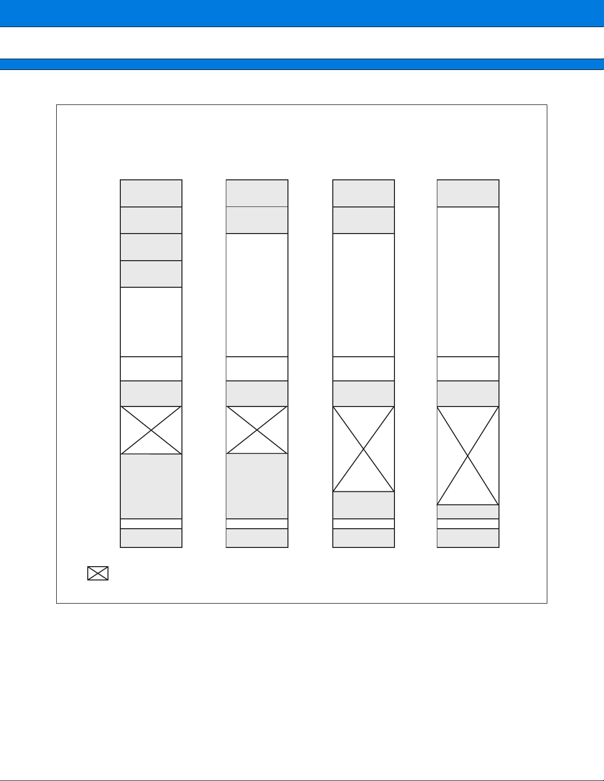
MEMORY MAP
■■■■
FFFFFFH
FF0000H
FEFFFFH
FE0000H
FDFFFFH
FD0000H
FCFFFFH
FC0000H
FBFFFFH
FB0000H
FAFFFFH
FA0000H
F9FFFFH
F90000H
F8FFFFH
F80000H
00FFFFH
008000H
007FFFH
007900H
0078FFH
MB90V340
ROM(FF bank)
ROM(FE bank)
ROM(FD bank)
ROM(FC bank)
ROM(FB bank)
ROM(FA bank)
ROM(F9 bank)
ROM(F8 bank)
ROM
(Image of FF bank)
Peripheral
FFFFFFH
FF0000H
FEFFFFH
FE0000H
FDFFFFH
FD0000H
FCFFFFH
FC0000H
FBFFFFH
FB0000H
FAFFFFH
FA0000H
F9FFFFH
F90000H
F8FFFFH
F80000H
00FFFFH
008000H
007FFFH
007900H
MB90F345/C/S/CS MB90F343/C/S/CS
ROM(FF bank)
ROM(FE bank)
ROM(FD bank)
FFFFFFH
FF0000H
FEFFFFH
FE0000H
FDFFFFH
FD0000H
FCFFFFH
ROM(FF bank)
ROM(FE bank)
ROM(FD bank)
ROM(FC bank)
FC0000H
ROM(FB bank)
ROM(FA bank)
ROM(F9 bank)
FBFFFFH
FB0000H
FAFFFFH
FA0000H
F9FFFFH
F90000H
F8FFFFH
ROM(FB bank)
ROM(FA bank)
ROM(F9 bank)
ROM(F8 bank)
F80000H
ROM
(Image of FF bank)
Peripheral
00FFFFH
008000H
007FFFH
007900H
ROM
(Image of FF bank)
Peripheral
28
000100H
0000EFH
000000H
RAM 30 K
Peripheral
: No access
0050FFH
000100H
0000EFH
000000H
RAM 20 K
Peripheral
0050FFH
000100H
0000EFH
000000H
RAM 20 K
Peripheral
Page 29
FFFFFFH
FF0000H
FEFFFFH
FE0000H
FDFFFFH
FD0000H
FCFFFFH
FC0000H
MB90349/C/S/CS
MB90342/C/S/CS
MB90F349/C/S/CS
MB90F342/C/S/CS
ROM (FF bank)
ROM (FE bank)
ROM (FD bank)
ROM (FC bank)
FFFFFFH
FF0000H
FEFFFFH
FE0000H
MB90348/C/S/CS
MB90341/C/S/CS
ROM (FF bank)
ROM (FE bank)
MB90347A/CA/AS/CAS
MB90F347A/CA/AS/CAS
FFFFFFH
FF0000H
FEFFFFH
FE0000H
ROM (FF bank)
ROM (FE bank)
MB90340 Series
MB90346A/CA/AS/CAS
MB90F346A/CA/AS/CAS
FFFFFFH
FF0000H
ROM (FF bank)
00FFFFH
008000H
007FFFH
007900H
003FFFH
000100H
0000EFH
000000H
ROM
(Image of FF bank)
Peripheral
RAM 16 K
Peripheral
00FFFFH
008000H
007FFFH
007900H
003FFFH
000100H
0000EFH
000000H
ROM
(Image of FF bank)
Peripheral
00FFFFH
008000H
007FFFH
007900H
ROM
(Image of FF bank)
Peripheral
RAM 16 K
0018FEH
RAM 6 K
000100H
Peripheral Peripheral
0000EFH
000000H
00FFFFH
008000H
007FFFH
007900H
0008FFH
000100H
0000EFH
000000H
ROM
(Image of FF bank)
Peripheral
RAM 2 K
Peripheral
: No access
Note : The high-order portion of bank 00 gives the image of the FF bank ROM to make the small model of the C
compiler effective. Since the low-order 16 bits are the same, the table in ROM can be referenced without
using the far specification in the pointer declaration.
For example, an attempt to access 00C000
H accesses the value at FFC000H in ROM.
The ROM area in bank FF exceeds 32 Kbytes, and its entire image cannot be shown in bank 00.
The image between FF8000
FF7FFF
H is visible only in bank FF.
H and FFFFFFH is visible in bank 00, while the image between FF0000H and
29
Page 30

MB90340 Series
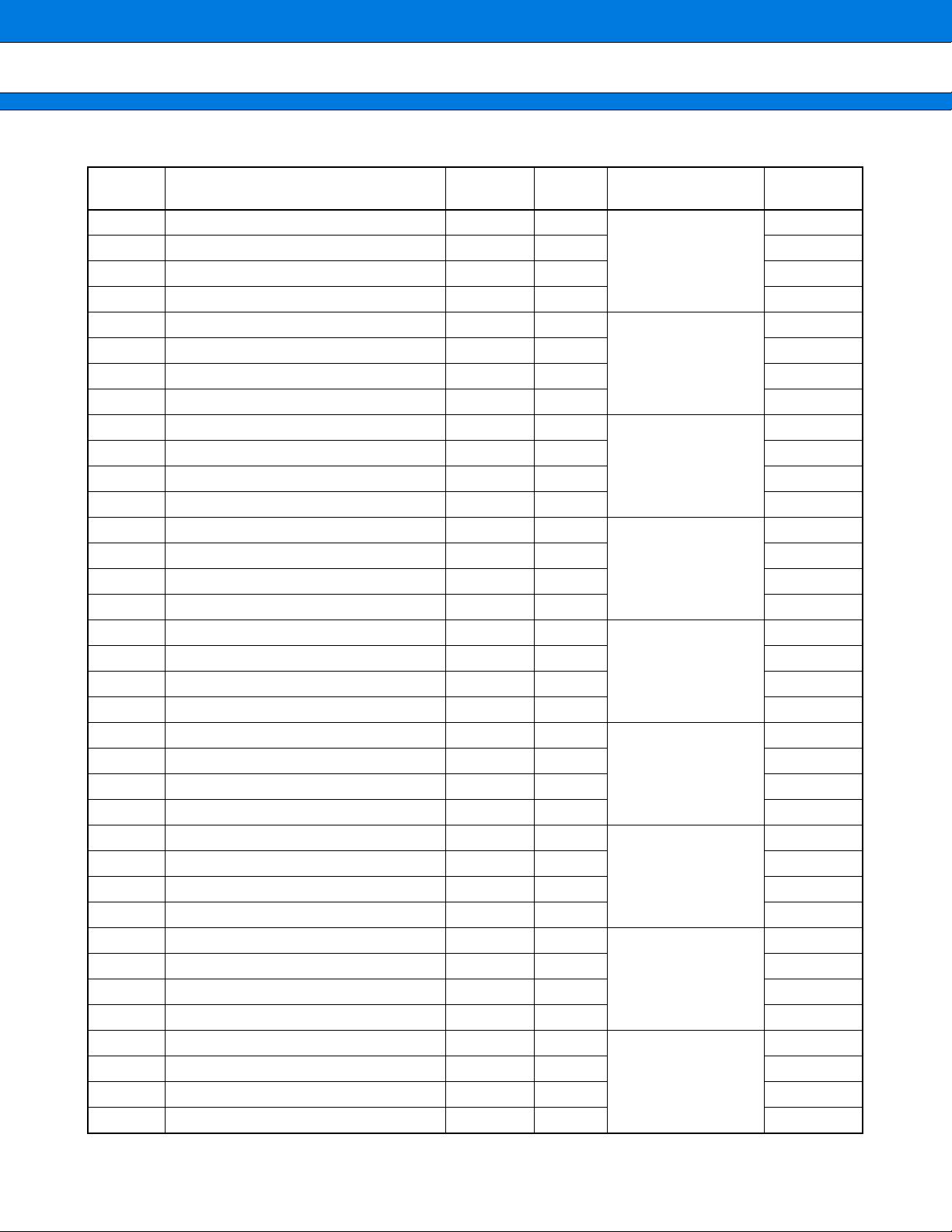
I/O MAP
■■■■
Address Register
00
H Port 0 data register PDR0 R/W Port 0 XXXXXXXX
01
H Port 1 data register PDR1 R/W Port 1 XXXXXXXX
02
H Port 2 data register PDR2 R/W Port 2 XXXXXXXX
Abbrevia-
tion
Access Resource name Initial value
03H Port 3 data register PDR3 R/W Port 3 XXXXXXXX
04
H Port 4 data register PDR4 R/W Port 4 XXXXXXXX
05
H Port 5 data register PDR5 R/W Port 5 XXXXXXXX
06H Port 6 data register PDR6 R/W Port 6 XXXXXXXX
07
H Port 7 data register PDR7 R/W Port 7 XXXXXXXX
08
H Port 8 data register PDR8 R/W Port 8 XXXXXXXX
09H Port 9 data register PDR9 R/W Port 9 XXXXXXXX
0A
H Port A data register PDRA R/W Port A XXXXXXXX
0B
H Analog Input Enable Port 5 ADER5 R/W Port 5, A/D 11111111
0CH Analog Input Enable Port 6 ADER6 R/W Port 6, A/D 11111111
0D
H Analog Input Enable Port 7 ADER7 R/W Port 7, A/D 11111111
0E
H Input level select register 0 ILSR0 R/W Ports XXXXXXXX
0FH Input level select register 1 ILSR1 R/W Ports XXXXXXXX
10
H Port 0 direction register DDR0 R/W Port 0 00000000
11
H Port 1 direction register DDR1 R/W Port 1 00000000
12
H Port 2 direction register DDR2 R/W Port 2 00000000
13H Port 3 direction register DDR3 R/W Port 3 00000000
14
H Port 4 direction register DDR4 R/W Port 4 00000000
15
H Port 5 direction register DDR5 R/W Port 5 00000000
16H Port 6 direction register DDR6 R/W Port 6 00000000
17
H Port 7 direction register DDR7 R/W Port 7 00000000
18
H Port 8 direction register DDR8 R/W Port 8 00000000
19H Port 9 direction register DDR9 R/W Port 9 00000000
1A
H Port A direction register DDRA R/W Port A 00000100
1B
H Reserved
1CH Port 0 Pullup control register PUCR0 R/W Port 0 00000000
1D
H Port 1 Pullup control register PUCR1 R/W Port 1 00000000
1E
H Port 2 Pullup control register PUCR2 R/W Port 2 00000000
1F
H Port 3 Pullup control register PUCR3 W, R/W Port 3 00000000
(Continued)
30
Page 31

MB90340 Series
Address Register
20
H Serial Mode Register SMR0 W,R/W
21
H Serial Control Register SCR0 W,R/W 00000000
22
H Reception/Transmission Data Register
23
H Serial Status Register SSR0 R,R/W 00001000
Abbrevia-
tion
RDR0/
TDR0
Access Resource name Initial value
00000000
R/W 00000000
UART0
24H Extended Communication Control Reg. ECCR0
25
H Extended Status/Control Register ESCR0 R/W 00000100
26
H Baud Rate Register 0 BGR00 R/W 00000000
R,W,R/
W
000000XX
27H Baud Rate Register 1 BGR01 R/W 00000000
28
H Serial Mode Register SMR1 W,R/W
29
H Serial Control Register SCR1 W,R/W 00000000
2AH Reception/Transmission Data Register
2B
H Serial Status Register SSR1 R,R/W 00001000
RDR1/
TDR1
R/W 00000000
00000000
UART1
2C
H Extended Communication Control Reg. ECCR1
R,W,
R/W
000000XX
2DH Extended Status/Control Register ESCR1 R/W 00000100
2E
H Baud Rate Register 0 BGR10 R/W 00000000
2F
H Baud Rate Register 1 BGR11 R/W 00000000
30
H PPG 0 operation mode control register PPGC0 W,R/W
31H PPG 1 operation mode control register PPGC1 W,R/W 0X000001
32
H PPG 0 and PPG 1 clock select register PPG01 R/W 000000X0
33
H Reserved
34H PPG 2 operation mode control register PPGC2 W,R/W
35
H PPG 3 operation mode control register PPGC3 W,R/W 0X000001
36
H PPG 2 and PPG 3 clock select register PPG23 R/W 000000X0
16-bit Programable
Pulse
Generator 0/1
16-bit Programable
Pulse
Generator 2/3
0X000XX1
0X000XX1
37H Reserved
38
H PPG 4 operation mode control register PPGC4 W,R/W
39
H PPG 5 operation mode control register PPGC5 W,R/W 0X000001
3AH PPG 4 and PPG 5 clock select register PPG45 R/W 000000X0
3B
H ROM Correction Control Status 1 PACSR1 R/W ROM Correction 1 00000000
3C
H PPG 6 operation mode control register PPGC6 W,R/W
3D
H PPG 7 operation mode control register PPGC7 W,R/W 0X000001
3EH PPG 6 and PPG 7 clock select register PPG67 R/W 000000X0
3F
H Reserved
16-bit Programable
Pulse
Generator 4/5
16-bit Programable
Pulse
Generator 6/7
0X000XX1
0X000XX1
(Continued)
31
Page 32

MB90340 Series
Address Register
40
H PPG 8 operation mode control register PPGC8 W,R/W
41
H PPG 9 operation mode control register PPGC9 W,R/W 0X000001
42
H PPG 8 and PPG 9 clock select register PPG89 R/W 000000X0
43
H Reserved
44H PPG A operation mode control register PPGCA W,R/W
45
H PPG B operation mode control register PPGCB W,R/W 0X000001
46
H PPG A and PPG B clock select register PPGAB R/W 000000X0
Abbrevia-
tion
Access Resource name Initial value
16-bit Programable
0X000XX1
Pulse
Generator 8/9
16-bit Programable
0X000XX1
Pulse
Generator A/B
47H Reserved
48
H PPG C operation mode control register PPGCC W,R/W
49
H PPG D operation mode control register PPGCD W,R/W 0X000001
4AH PPG C and PPG D clock select register PPGCD R/W 000000X0
4B
H Reserved
4C
H PPG E operation mode control register PPGCE W,R/W
4DH PPG F operation mode control register PPGCF W,R/W 0X000001
4E
H PPG E and PPG F clock select register PPGEF R/W 000000X0
4F
H Reserved
16-bit Programable
Pulse
Generator C/D
16-bit Programable
Pulse
Generator E/F
0X000XX1
0X000XX1
50
H Input Capture Control Status 0/1 ICS01 R/W
00000000
Input Capture 0/1
51H Input Capture Edge 0/1 ICE01 R/W XXX0X0XX
52
H Input Capture Control Status 2/3 ICS23 R/W
00000000
Input Capture 2/3
53
H Input Capture Edge 2/3 ICE23 R/W XXXXXXXX
54H Input Capture Control Status 4/5 ICS45 R/W
00000000
Input Capture 4/5
55
H Input Capture Edge 4/5 ICE45 R/W XXXXXXXX
56
H Input Capture Control Status 6/7 ICS67 R/W
00000000
Input Capture 6/7
57H Input Capture Edge 6/7 ICE67 R/W XXX000XX
58
H Output Compare Control Status 0 OCS0 R/W
0000XX00
Output Compare 0/1
59
H Output Compare Control Status 1 OCS1 R/W 0XX00000
5AH Output Compare Control Status 2 OCS2 R/W
0000XX00
Output Compare 2/3
5B
H Output Compare Control Status 3 OCS3 R/W 0XX00000
5C
H Output Compare Control Status 4 OCS4 R/W
0000XX00
Output Compare 4/5
5DH Output Compare Control Status 5 OCS5 R/W 0XX00000
5E
H Output Compare Control Status 6 OCS6 R/W
0000XX00
Output Compare 6/7
5F
H Output Compare Control Status 7 OCS7 R/W 0XX00000
(Continued)
32
Page 33

MB90340 Series
Address Register
60
H Timer Control Status 0 TMCSR0 R/W
Abbrevia-
tion
Access Resource name Initial value
00000000
16-bit Reload Timer 0
61
H Timer Control Status 0 TMCSR0 R/W XXXX0000
62
H Timer Control Status 1 TMCSR1 R/W
00000000
16-bit Reload Timer 1
63
H Timer Control Status 1 TMCSR1 R/W XXXX0000
64H Timer Control Status 2 TMCSR2 R/W
00000000
16-bit Reload Timer 2
65
H Timer Control Status 2 TMCSR2 R/W XXXX0000
66
H Timer Control Status 3 TMCSR3 R/W
00000000
16-bit Reload Timer 3
67H Timer Control Status 3 TMCSR3 R/W XXXX0000
68
H A/D Control Status 0 ADCS0 R/W
69
H A/D Control Status 1 ADCS1 R/W 0000000X
000XXXX0
6AH A/D Data 0 ADCR0 R 00000000
A/D Converter
6B
H A/D Data 1 ADCR1 R XXXXXX00
6C
H ADC Setting 0 ADSR0 R/W 00000000
6DH ADC Setting 1 ADSR1 R/W 00000000
6E
H Reserved
6F
H ROM Mirror ROMM W ROM Mirror XXXXXXX1
70
H to 8FH Reserved for CAN Interface 0/1. Refer to “■ CAN CONTROLLERS”
90H to 9AH Reserved
9B
H DMA Descriptor Channel Select DCSR R/W
9C
H DMA Status L DSRL R/W 00000000
DMA
00000000
9DH DMA Status H DSRH R/W 00000000
9E
H ROM Correction Control Status 0 PACSR0 R/W ROM Correction 0 00000000
9F
H Delayed Interrupt/release DIRR R/W Delayed Interrupt XXXXXXX0
A0H Low-power Mode Control LPMCR W,R/W
A1
H Clock Selection CKSCR R,R/W
A2
H, A3H Reserved
Low Power
Controller
Low Power
Controller
00011000
11111100
A4H DMA Stop Status DSSR R/W DMA 00000000
A5
H Automatic ready function select reg. ARSR W
A6
H External address output control reg. HACR W 00000000
External Memory
Access
0011XX00
A7H Bus control signal selection register ECSR W 0000000X
A8
H Watchdog Control WDTC R,W Watchdog Timer XXXXX111
A9
H Time Base Timer Control TBTC W,R/W Time Base Timer 1XX00100
(Continued)
33
Page 34

MB90340 Series
Address Register
AA
H Watch Timer Control register WTC R,R/W Watch Timer 1X001000
AB
H Reserved
AC
H DMA Enable L DERL R/W
Abbrevia-
tion
Access Resource name Initial value
00000000
DMA
AD
H DMA Enable H DERH R/W 00000000
Flash Control Status
AEH
(FlashDevices only.
FMCS R,R/W Flash Memory 000X0000
Otherwise reserved)
AF
H Reserved
B0
H Interrupt control register 00 ICR00 W,R/W
00000111
B1H Interrupt control register 01 ICR01 W,R/W 00000111
B2
H Interrupt control register 02 ICR02 W,R/W 00000111
B3
H Interrupt control register 03 ICR03 W,R/W 00000111
B4H Interrupt control register 04 ICR04 W,R/W 00000111
B5
H Interrupt control register 05 ICR05 W,R/W 00000111
B6
H Interrupt control register 06 ICR06 W,R/W 00000111
B7H Interrupt control register 07 ICR07 W,R/W 00000111
Interrupt controller
B8
H Interrupt control register 08 ICR08 W,R/W 00000111
B9
H Interrupt control register 09 ICR09 W,R/W 00000111
BA
H Interrupt control register 10 ICR10 W,R/W 00000111
BBH Interrupt control register 11 ICR11 W,R/W 00000111
BC
H Interrupt control register 12 ICR12 W,R/W 00000111
BD
H Interrupt control register 13 ICR13 W,R/W 00000111
BEH Interrupt control register 14 ICR14 W,R/W 00000111
BF
H Interrupt control register 15 ICR15 W,R/W 00000111
C0
H D/A Converter data 0 DAT0 R/W
XXXXXXXX
C1H D/A Converter data 1 DAT1 R/W XXXXXXXX
D/A Converter
C2
H D/A Control 0 DACR0 R/W XXXXXXX0
C3
H D/A Control 1 DACR1 R/W XXXXXXX0
C4H, C5H Reserved
C6
H External Interrupt Enable 0 ENIR0 R/W
C7
H External Interrupt Request 0 EIRR0 R/W XXXXXXXX
00000000
External Interrupt 0
C8H External Interrupt Level 0 ELVR0 R/W 00000000
C9
H External Interrupt Level 0 ELVR0 R/W 00000000
(Continued)
34
Page 35

MB90340 Series
Address Register
CA
H External Interrupt Enable 1 ENIR1 R/W
CB
H External Interrupt Request 1 EIRR1 R/W XXXXXXXX
CC
H External Interrupt Level 1 ELVR1 R/W 00000000
CD
H External Interrupt Level 1 ELVR1 R/W 00000000
Abbrevia-
tion
Access Resource name Initial value
00000000
External Interrupt 1
CEH External Interrupt 1 Source Select EISSR R/W 00000000
CF
H PLL/Subclock Control register PSCCR W PLL XXXX0000
D0
H DMA Buffer Addrss Pointer L BAPL R/W
XXXXXXXX
D1H DMA Buffer Addrss Pointer M BAPM R/W XXXXXXXX
D2
H DMA Buffer Addrss Pointer H BAPH R/W XXXXXXXX
D3
H DMA Control DMACS R/W XXXXXXXX
DMA
D4H I/O Register Address Pointer L IOAL R/W XXXXXXXX
D5
H I/O Register Address Pointer H IOAH R/W XXXXXXXX
D6
H Data Counter L DCTL R/W XXXXXXXX
D7H Data Counter H DCTH R/W XXXXXXXX
D8
H Serial Mode Register SMR2 W,R/W
D9
H Serial Control Register SCR2 W,R/W 00000000
00000000
DA
H Reception/Transmission Data Register
RDR2/
TDR2
R/W 00000000
DBH Serial Status Register SSR2 R,R/W 00001000
UART2
DC
H Extended Communication Control Reg. ECCR2
DD
H Extended Status/Control Register ESCR2 R/W 00000100
R,W,
R/W
000000XX
DEH Baud Rate Register 0 BGR20 R/W 00000000
DF
H Baud Rate Register 1 BGR21 R/W 00000000
E0
H to EFH Reserved for CAN Interface 2. Refer to “■ CAN CONTROLLERS”
F0H to FFH External
(Continued)
35
Page 36
MB90340 Series
Address Register
7900
H Reload L PRLL0 R/W
7901
H Reload H PRLH0 R/W XXXXXXXX
Abbrevia-
tion
Access Resource name Initial value
16-bit Programable
Pulse
H Reload L PRLL1 R/W XXXXXXXX
7902
H Reload H PRLH1 R/W XXXXXXXX
7903
7904
H Reload L PRLL2 R/W
H Reload H PRLH2 R/W XXXXXXXX
7905
Generator 0/1
16-bit Programable
Pulse
7906
H Reload L PRLL3 R/W XXXXXXXX
H Reload H PRLH3 R/W XXXXXXXX
7907
7908
H Reload L PRLL4 R/W
H Reload H PRLH4 R/W XXXXXXXX
7909
Generator 2/3
16-bit Programable
Pulse
H Reload L PRLL5 R/W XXXXXXXX
790A
790B
H Reload H PRLH5 R/W XXXXXXXX
H Reload L PRLL6 R/W
790C
790D
H Reload H PRLH6 R/W XXXXXXXX
Generator 4/5
16-bit Programable
Pulse
H Reload L PRLL7 R/W XXXXXXXX
790E
790F
H Reload H PRLH7 R/W XXXXXXXX
H Reload L PRLL8 R/W
7910
H Reload H PRLH8 R/W XXXXXXXX
7911
Generator 6/7
16-bit Programable
Pulse
H Reload L PRLL9 R/W XXXXXXXX
7912
7913
H Reload H PRLH9 R/W XXXXXXXX
H Reload L PRLLA R/W
7914
H Reload H PRLHA R/W XXXXXXXX
7915
Generator 8/9
16-bit Programable
Pulse
H Reload L PRLLB R/W XXXXXXXX
7916
H Reload H PRLHB R/W XXXXXXXX
7917
7918
H Reload L PRLLC R/W
H Reload H PRLHC R/W XXXXXXXX
7919
Generator A/B
16-bit Programable
Pulse
H Reload L PRLLD R/W XXXXXXXX
791A
H Reload H PRLHD R/W XXXXXXXX
791B
H Reload L PRLLE R/W
791C
H Reload H PRLHE R/W XXXXXXXX
791D
Generator C/D
16-bit Programable
Pulse
H Reload L PRLLF R/W XXXXXXXX
791E
H Reload H PRLHF R/W XXXXXXXX
791F
H Input Capture 0 IPCP0 R
7920
H Input Capture 0 IPCP0 R XXXXXXXX
7921
Generator E/F
Input Capture 0/1
H Input Capture 1 IPCP1 R XXXXXXXX
7922
H Input Capture 1 IPCP1 R XXXXXXXX
7923
XXXXXXXX
XXXXXXXX
XXXXXXXX
XXXXXXXX
XXXXXXXX
XXXXXXXX
XXXXXXXX
XXXXXXXX
XXXXXXXX
(Continued)
36
Page 37

MB90340 Series
Address Register
7924
H Input Capture 2 IPCP2 R
7925
H Input Capture 2 IPCP2 R XXXXXXXX
Abbrevia-
tion
Access Resource name Initial value
Input Capture 2/3
H Input Capture 3 IPCP3 R XXXXXXXX
7926
H Input Capture 3 IPCP3 R XXXXXXXX
7927
7928
H Input Capture 4 IPCP4 R
H Input Capture 4 IPCP4 R XXXXXXXX
7929
Input Capture 4/5
792A
H Input Capture 5 IPCP5 R XXXXXXXX
H Input Capture 5 IPCP5 R XXXXXXXX
792B
792C
H Input Capture 6 IPCP6 R
H Input Capture 6 IPCP6 R XXXXXXXX
792D
Input Capture 6/7
H Input Capture 7 IPCP7 R XXXXXXXX
792E
792F
H Input Capture 7 IPCP7 R XXXXXXXX
H Output Compare 0 OCCP0 R/W
7930
7931
H Output Compare 0 OCCP0 R/W XXXXXXXX
Output Compare 0/1
H Output Compare 1 OCCP1 R/W XXXXXXXX
7932
7933
H Output Compare 1 OCCP1 R/W XXXXXXXX
H Output Compare 2 OCCP2 R/W
7934
H Output Compare 2 OCCP2 R/W XXXXXXXX
7935
Output Compare 2/3
H Output Compare 3 OCCP3 R/W XXXXXXXX
7936
7937
H Output Compare 3 OCCP3 R/W XXXXXXXX
H Output Compare 4 OCCP4 R/W
7938
H Output Compare 4 OCCP4 R/W XXXXXXXX
7939
Output Compare 4/5
H Output Compare 5 OCCP5 R/W XXXXXXXX
793A
H Output Compare 5 OCCP5 R/W XXXXXXXX
793B
793C
H Output Compare 6 OCCP6 R/W
H Output Compare 6 OCCP6 R/W XXXXXXXX
793D
Output Compare 6/7
H Output Compare 7 OCCP7 R/W XXXXXXXX
793E
H Output Compare 7 OCCP7 R/W XXXXXXXX
793F
H Timer Data 0 TCDT0 R/W
7940
H Timer Data 0 TCDT0 R/W 00000000
7941
I/O Timer 0
H Timer Control 0 TCCSL0 R/W 00000000
7942
H Timer Control 0 TCCSH0 R/W 0XXXXXXX
7943
H Timer Data 1 TCDT1 R/W
7944
H Timer Data 1 TCDT1 R/W 00000000
7945
I/O Timer 1
H Timer Control 1 TCCSL1 R/W 00000000
7946
H Timer Control 1 TCCSH1 R/W 0XXXXXXX
7947
XXXXXXXX
XXXXXXXX
XXXXXXXX
XXXXXXXX
XXXXXXXX
XXXXXXXX
XXXXXXXX
00000000
00000000
(Continued)
37
Page 38

MB90340 Series
Address Register
7948
H
Timer 0/Reload 0
7949
H R/W XXXXXXXX
H
794A
Timer 1/Reload 1
H R/W XXXXXXXX
794B
794C
H
Timer 2/Reload 2
H R/W XXXXXXXX
794D
794E
H
Timer 3/Reload 3
H R/W XXXXXXXX
794F
7950
H Serial Mode Register SMR3 W,R/W
H Serial Control Register SCR3 W,R/W 00000000
7951
H Reception/Transmission Data Register
7952
H Serial Status Register SSR3 R,R/W 00001000
7953
Abbrevia-
tion
TMR0/
TMRLR0
TMR1/
TMRLR1
TMR2/
TMRLR2
TMR3/
TMRLR3
RDR3/
TDR3
Access Resource name Initial value
R/W
16-bit Reload
Timer 0
R/W
16-bit Reload
Timer 1
R/W
16-bit Reload
Timer 2
R/W
16-bit Reload
Timer 3
R/W 00000000
UART3
H Extended Communication Control Reg. ECCR3
7954
H Extended Status/Control Register ESCR3 R/W 00000100
7955
7956
H Baud Rate Register 0 BGR30 R/W 00000000
H Baud Rate Register 1 BGR31 R/W 00000000
7957
H Serial Mode Register SMR4 W,R/W
7958
H Serial Control Register SCR4 W,R/W 00000000
7959
H Reception/Transmission Data Register
795A
H Serial Status Register SSR4 R,R/W 00001000
795B
RDR4/
TDR4
R,W,
R/W
R/W 00000000
UART4
H Extended Communication Control Reg. ECCR4
795C
H Extended Status/Control Register ESCR4 R/W 00000100
795D
H Baud Rate Register 0 BGR40 R/W 00000000
795E
H Baud Rate Register 1 BGR41 R/W 00000000
795F
H to
7960
796B
H
H Clock output enable register CLKR R/W Clock Monitor XXXX0000
796C
H Reserved
796D
796E
H CAN Direct Mode Register CDMR R/W CAN clock sync XXXXXXX0
H CAN RX/TX redirect register CANSWR R/W CAN 0/1 XXXXXX00
796F
Reserved
R,W,
R/W
XXXXXXXX
XXXXXXXX
XXXXXXXX
XXXXXXXX
00000000
000000XX
00000000
000000XX
(Continued)
38
Page 39

MB90340 Series
Address Register
7970
7971
7972
2
H I
C bus status register IBSR0 R
2
H I
C bus control register IBCR0 W,R/W 00000000
H
Abbrevia-
tion
Access Resource name Initial value
ITBAL0 R/W 00000000
I2C 10 bit slave address register
H ITBAH0 R/W 00000000
7973
7974
H
ITMKL0 R/W 11111111
2
I
C Interface 0
I2C 10 bit address mask register
H ITMKH0 R/W 00111111
7975
7976
7977
7978
7979
797A
797B
797C
797F
7980
7981
7982
2
H I
C 7 bit slave address register ISBA0 R/W 00000000
2
H I
C 7 bit address mask register ISMK0 R/W 01111111
2
H I
C data register IDAR0 R/W 00000000
H,
H
2
H I
C clock control register ICCR0 R/W I2C Interface 0 00011111
H to
H
2
H I
C bus status register IBSR1 R
2
H I
C bus control register IBCR1 W,R/W 00000000
H
Reserved
Reserved
ITBAL1 R/W 00000000
I2C 10 bit slave address register
H ITBAH1 R/W 00000000
7983
2
I
7984
H
ITMKL1 R/W 11111111
C Interface 1
I2C 10 bit address mask register
H ITMKH1 R/W 00111111
7985
7986
7987
7988
7989
798A
798B
798C
79C1
79C2
79C3
79DF
2
H I
C 7 bit slave address register ISBA1 R/W 00000000
2
H I
C 7 bit address mask register ISMK1 R/W 01111111
2
H I
C data register IDAR1 R/W 00000000
H,
H
2
H I
C clock control register ICCR1 R/W I2C Interface 1 00011111
H to
H
H Clock Modulator Control Register CMCR R,R/W Clock Modulator 0001X000
H to
H
Reserved
Reserved
Reserved
00000000
00000000
(Continued)
39
Page 40

MB90340 Series
(Continued)
Address Register
79E0
H ROM Correction Address 0 PADR0 R/W
79E1
H ROM Correction Address 0 PADR0 R/W XXXXXXXX
H ROM Correction Address 0 PADR0 R/W XXXXXXXX
79E2
H ROM Correction Address 1 PADR1 R/W XXXXXXXX
79E3
79E4
H ROM Correction Address 1 PADR1 R/W XXXXXXXX
H ROM Correction Address 1 PADR1 R/W XXXXXXXX
79E5
79E6
H ROM Correction Address 2 PADR2 R/W XXXXXXXX
H ROM Correction Address 2 PADR2 R/W XXXXXXXX
79E7
79E8
H ROM Correction Address 2 PADR2 R/W XXXXXXXX
H to
79E9
79EF
H
H ROM Correction Address 3 PADR3 R/W
79F0
H ROM Correction Address 3 PADR3 R/W XXXXXXXX
79F1
79F2
H ROM Correction Address 3 PADR3 R/W XXXXXXXX
H ROM Correction Address 4 PADR4 R/W XXXXXXXX
79F3
79F4
H ROM Correction Address 4 PADR4 R/W XXXXXXXX
H ROM Correction Address 4 PADR4 R/W XXXXXXXX
79F5
H ROM Correction Address 5 PADR5 R/W XXXXXXXX
79F6
H ROM Correction Address 5 PADR5 R/W XXXXXXXX
79F7
79F8
H ROM Correction Address 5 PADR5 R/W XXXXXXXX
H to
79F9
79FF
H
H to
7A00
7AFF
7B00
7BFF
7C00
7CFF
7D00
7DFF
7E00
7EFF
7F00
7FFF
H
H to
H
H to
H
H to
H
H to
H
H to
H
Reserved for CAN Interface 0. Refer to “■ CAN CONTROLLERS”
Reserved for CAN Interface 0. Refer to “■ CAN CONTROLLERS”
Reserved for CAN Interface 1. Refer to “■ CAN CONTROLLERS”
Reserved for CAN Interface 1. Refer to “■ CAN CONTROLLERS”
Reserved for CAN Interface 2. Refer to “■ CAN CONTROLLERS”
Reserved for CAN Interface 2. Refer to “■ CAN CONTROLLERS”
Abbrevia-
tion
Reserved
Reserved
Access Resource name Initial value
XXXXXXXX
ROM Correction 0
XXXXXXXX
ROM Correction 1
Notes : • Initial value of “X” represents unknown value.
• Addresses in the range 0000
H to 00BFH, which are not listed in the table, are reserved for the primary
functions of the MCU. A read access to these reserved addresses results reading “X” and any write
access should not be performed.
40
Page 41

MB90340 Series
CAN CONTROLLERS
■■■■
The CAN controller has the following features :
• Conforms to CAN Specification Version 2.0 Part A and B
• Supports transmission/reception in standard frame and extended frame formats
• Supports transmitting of data frames by receiving remote frames
• 16 transmitting/receiving message buffers
• 29-bit ID and 8-byte data
• Multi-level message buffer configuration
• Provides full-bit comparison, full-bit mask, acceptance register 0/acceptance register 1 for each message
buffer as ID acceptance mask
• Two acceptance mask registers in either standard frame format or extended frame formats
• Bit rate programmable from 10 Kbits/s to 2 Mbits/s (when input clock is at 16 MHz)
List of Control Registers (1)
Address
CAN0 CAN1 CAN2
000070
000071
H 000080H 0000E0H
H 000081H 0000E1H
000072H 000082H 0000E2H
000073
H 000083H 0000E3H
000074H 000084H 0000E4H
000075
H 000085H 0000E5H
000076H 000086H 0000E6H
000077
H 000087H 0000E7H
000078H 000088H 0000E8H
000079
H 000089H 0000E9H
00007AH 00008AH 0000EAH
00007B
H 00008BH 0000EBH
00007CH 00008CH 0000ECH
00007D
H 00008DH 0000EDH
00007EH 00008EH 0000EEH
00007F
H 00008FH 0000EFH
Register Abbreviation Access Initial Value
Message buffer
valid register
Transmit request
register
Transmit cancel
register
Transmission
complete register
Receive complete
register
Remote request
receiving register
Receive overrun
register
Reception interrupt
enable register
BVALR R/W
TREQR R/W
TCANR W
TCR R/W
RCR R/W
RRTRR R/W
ROVRR R/W
RIER R/W
00000000
00000000
00000000
00000000
00000000
00000000
00000000
00000000
00000000
00000000
00000000
00000000
00000000
00000000
00000000
00000000
41
Page 42
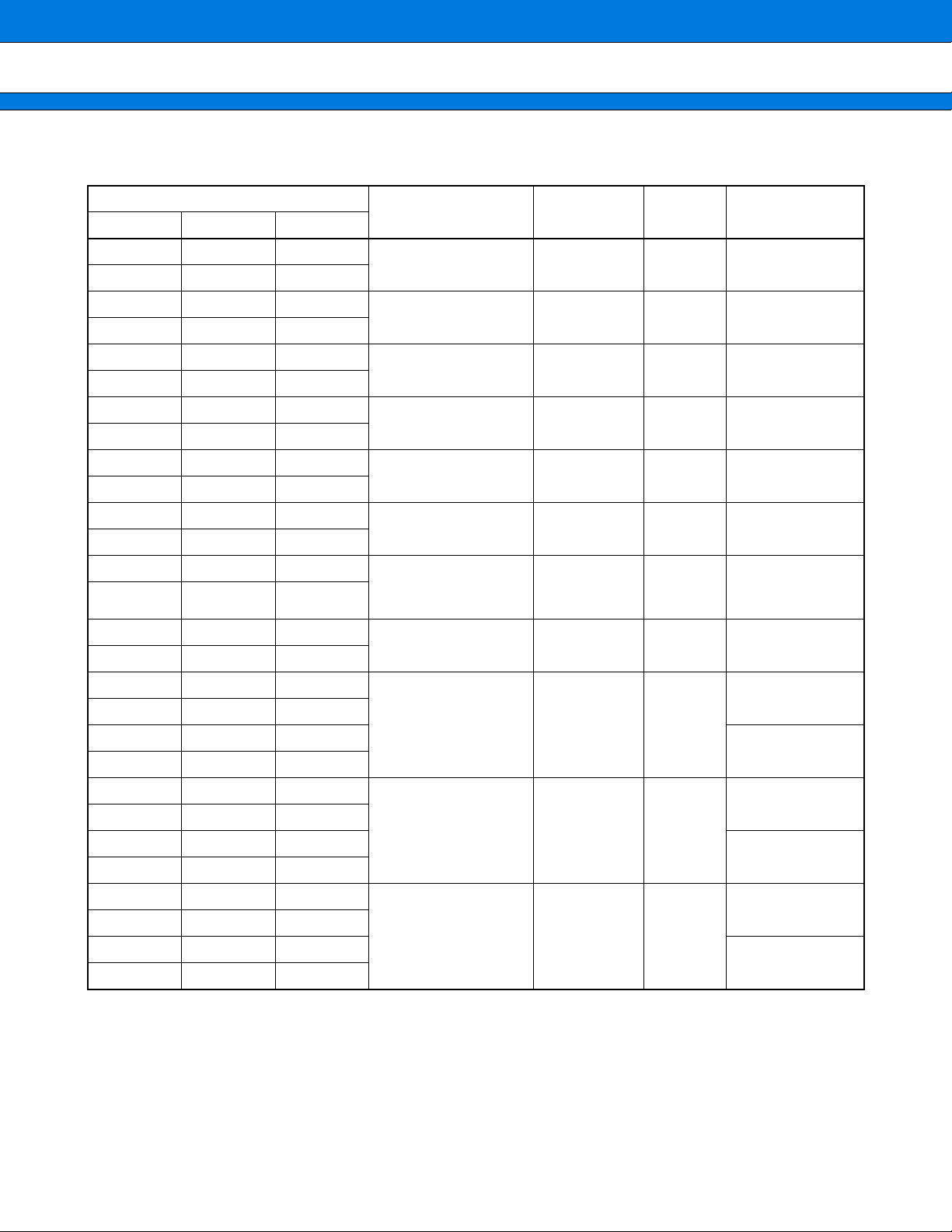
MB90340 Series
List of Control Registers (2)
Address
Register Abbreviation Access Initial Value
CAN0 CAN1 CAN2
007B00
007B01
007B02H 007D02H 007F02H
007B03
007B04H 007D04H 007F04H
007B05
007B06H 007D06H 007F06H
007B07
H 007D00H 007F00H
H 007D01H 007F01H
H 007D03H 007F03H
H 007D05H 007F05H
H 007D07H 007F07H
Control status
register
Last event
indicator register
Receive/transmit
error counter
Bit timing
register
007B08H 007D08H 007F08H
IDE register IDER R/W
007B09
007B0AH 007D0AH 007F0AH
007B0B
H 007D09H 007F09H
H 007D0BH 007F0BH
Transmit RTR
register
007B0CH 007D0CH 007F0CH Remote frame
receive waiting
007B0D
007B0EH 007D0EH 007F0EH
007B0F
H 007D0DH 007F0DH
H 007D0FH 007F0FH
register
Transmit interrupt
enable register
CSR
R/W, W
R/W, R
LEIR R/W
RTEC R
BTR R/W
TRTRR R/W
RFWTR R/W
TIER R/W
0XXXX0X1
00XXX000
000X0000
XXXXXXXX
00000000
00000000
11111111
X1111111
XXXXXXXX
XXXXXXXX
00000000
00000000
XXXXXXXX
XXXXXXXX
00000000
00000000
007B10H 007D10H 007F10H
007B11
H 007D11H 007F11H
007B12H 007D12H 007F12H
007B13
H 007D13H 007F13H
007B14H 007D14H 007F14H
007B15
H 007D15H 007F15H
007B16H 007D16H 007F16H
007B17
H 007D17H 007F17H
007B18H 007D18H 007F18H
007B19
H 007D19H 007F19H
007B1AH 007D1AH 007F1AH
007B1B
H 007D1BH 007F1BH
Acceptance mask
select register
Acceptance mask
register 0
Acceptance mask
register 1
XXXXXXXX
XXXXXXXX
AMSR R/W
XXXXXXXX
XXXXXXXX
XXXXXXXX
XXXXXXXX
AMR0 R/W
XXXXXXXX
XXXXXXXX
XXXXXXXX
XXXXXXXX
AMR1 R/W
XXXXXXXX
XXXXXXXX
42
Page 43
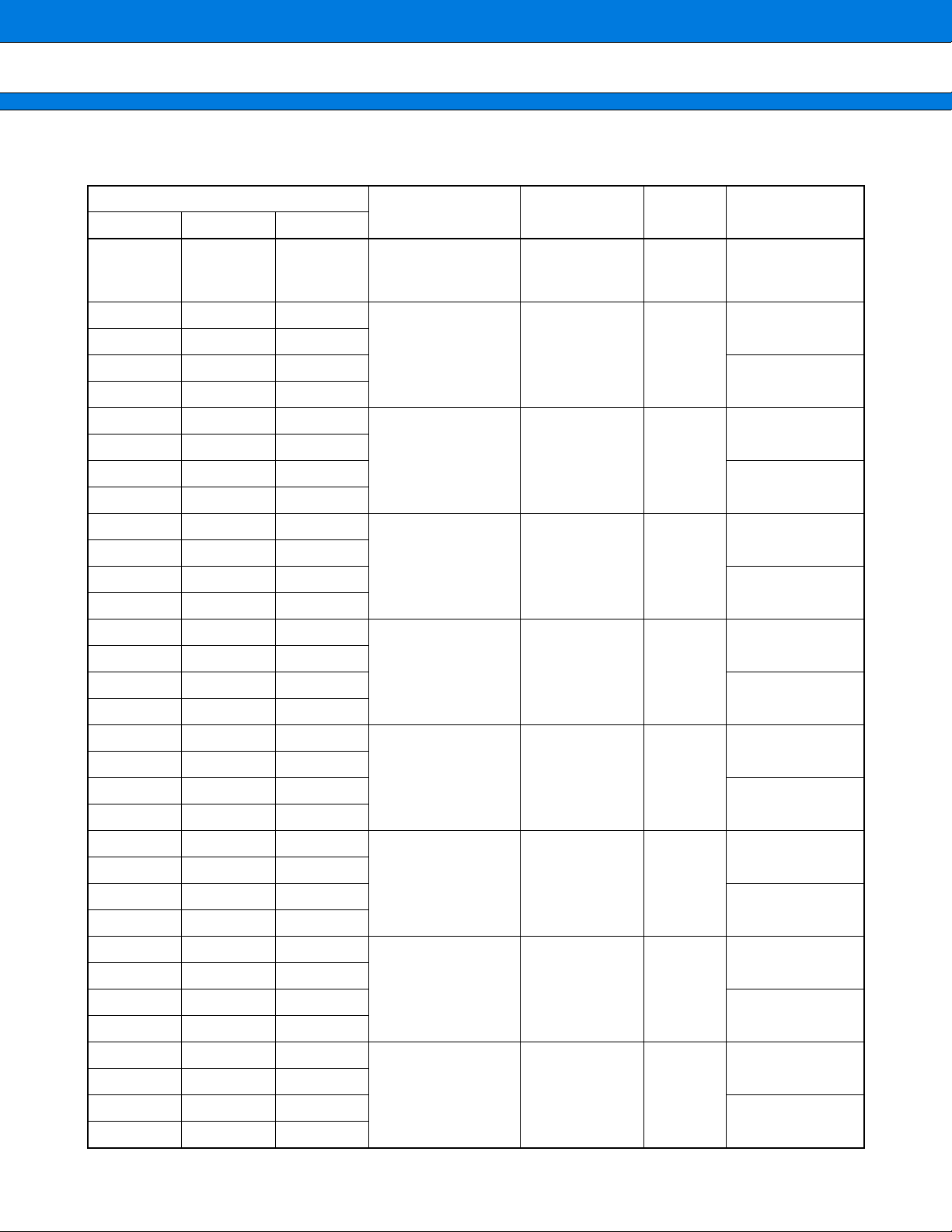
MB90340 Series
List of Message Buffers (ID Registers) (1)
Address
CAN0 CAN1 CAN2
007A00
007A1F
007A20
007A21
H
007C00H
to
H
H 007C20H 007E20H
H 007C21H 007E21H
to
007C1F
H
007E00H
to
007E1F
007A22H 007C22H 007E22H
007A23
H 007C23H 007E23H
007A24H 007C24H 007E24H
007A25
H 007C25H 007E25H
007A26H 007C26H 007E26H
007A27
H 007C27H 007E27H
007A28H 007C28H 007E28H
007A29
H 007C29H 007E29H
007A2AH 007C2AH 007E2AH
007A2B
H 007C2BH 007E2BH
007A2CH 007C2CH 007E2CH
007A2D
H 007C2DH 007E2DH
007A2EH 007C2EH 007E2EH
007A2F
H 007C2FH 007E2FH
007A30H 007C30H 007E30H
007A31
H 007C31H 007E31H
007A32H 007C32H 007E32H
007A33
H 007C33H 007E33H
Register Abbreviation Access Initial Value
General-
H
purpose RAM
R/W
XXXXXXXX
to
XXXXXXXX
XXXXXXXX
XXXXXXXX
ID register 0 IDR0 R/W
XXXXXXXX
XXXXXXXX
XXXXXXXX
XXXXXXXX
ID register 1 IDR1 R/W
XXXXXXXX
XXXXXXXX
XXXXXXXX
XXXXXXXX
ID register 2 IDR2 R/W
XXXXXXXX
XXXXXXXX
XXXXXXXX
XXXXXXXX
ID register 3 IDR3 R/W
XXXXXXXX
XXXXXXXX
XXXXXXXX
XXXXXXXX
ID register 4 IDR4 R/W
XXXXXXXX
XXXXXXXX
007A34H 007C34H 007E34H
007A35
H 007C35H 007E35H
007A36H 007C36H 007E36H
007A37
H 007C37H 007E37H
007A38H 007C38H 007E38H
007A39
H 007C39H 007E39H
007A3AH 007C3AH 007E3AH
007A3B
H 007C3BH 007E3BH
007A3CH 007C3CH 007E3CH
007A3D
H 007C3DH 007E3DH
007A3EH 007C3EH 007E3EH
007A3F
H 007C3FH 007E3FH
XXXXXXXX
XXXXXXXX
ID register 5 IDR5 R/W
XXXXXXXX
XXXXXXXX
XXXXXXXX
XXXXXXXX
ID register 6 IDR6 R/W
XXXXXXXX
XXXXXXXX
XXXXXXXX
XXXXXXXX
ID register 7 IDR7 R/W
XXXXXXXX
XXXXXXXX
43
Page 44

MB90340 Series
List of Message Buffers (ID Registers) (2)
Address
CAN0 CAN1 CAN2
007A40
007A41
H 007C40H 007E40H
H 007C41H 007E41H
007A42H 007C42H 007E42H
007A43
H 007C43H 007E43H
007A44H 007C44H 007E44H
007A45
H 007C45H 007E45H
007A46H 007C46H 007E46H
007A47
H 007C47H 007E47H
007A48H 007C48H 007E48H
007A49
H 007C49H 007E49H
007A4AH 007C4AH 007E4AH
007A4B
H 007C4BH 007E4BH
007A4CH 007C4CH 007E4CH
007A4D
H 007C4DH 007E4DH
007A4EH 007C4EH 007E4EH
007A4F
H 007C4FH 007E4FH
Register Abbreviation Access Initial Value
XXXXXXXX
XXXXXXXX
ID register 8 IDR8 R/W
XXXXXXXX
XXXXXXXX
XXXXXXXX
XXXXXXXX
ID register 9 IDR9 R/W
XXXXXXXX
XXXXXXXX
XXXXXXXX
XXXXXXXX
ID register 10 IDR10 R/W
XXXXXXXX
XXXXXXXX
XXXXXXXX
XXXXXXXX
ID register 11 IDR11 R/W
XXXXXXXX
XXXXXXXX
007A50H 007C50H 007E50H
007A51
H 007C51H 007E51H
007A52H 007C52H 007E52H
007A53
H 007C53H 007E53H
007A54H 007C54H 007E54H
007A55
H 007C55H 007E55H
007A56H 007C56H 007E56H
007A57
H 007C57H 007E57H
007A58H 007C58H 007E58H
007A59
H 007C59H 007E59H
007A5AH 007C5AH 007E5AH
007A5B
H 007C5BH 007E5BH
007A5CH 007C5CH 007E5CH
007A5D
H 007C5DH 007E5DH
007A5EH 007C5EH 007E5EH
007A5F
H 007C5FH 007E5FH
XXXXXXXX
XXXXXXXX
ID register 12 IDR12 R/W
XXXXXXXX
XXXXXXXX
XXXXXXXX
XXXXXXXX
ID register 13 IDR13 R/W
XXXXXXXX
XXXXXXXX
XXXXXXXX
XXXXXXXX
ID register 14 IDR14 R/W
XXXXXXXX
XXXXXXXX
XXXXXXXX
XXXXXXXX
ID register 15 IDR15 R/W
XXXXXXXX
XXXXXXXX
44
Page 45

MB90340 Series
List of Message Buffers (DLC Registers and Data Registers) (1)
Address
CAN0 CAN1 CAN2
007A60
007A61
H 007C60H 007E60H
H 007C61H 007E61H
007A62H 007C62H 007E62H
007A63
H 007C63H 007E63H
007A64H 007C64H 007E64H
007A65
H 007C65H 007E65H
007A66H 007C66H 007E66H
007A67
H 007C67H 007E67H
007A68H 007C68H 007E68H
007A69
H 007C69H 007E69H
007A6AH 007C6AH 007E6AH
007A6B
H 007C6BH 007E6BH
007A6CH 007C6CH 007E6CH
007A6D
H 007C6DH 007E6DH
007A6EH 007C6EH 007E6EH
007A6F
H 007C6FH 007E6FH
Register Abbreviation Access Initial Value
DLC register 0 DLCR0 R/W XXXXXXXX
DLC register 1 DLCR1 R/W XXXXXXXX
DLC register 2 DLCR2 R/W XXXXXXXX
DLC register 3 DLCR3 R/W XXXXXXXX
DLC register 4 DLCR4 R/W XXXXXXXX
DLC register 5 DLCR5 R/W XXXXXXXX
DLC register 6 DLCR6 R/W XXXXXXXX
DLC register 7 DLCR7 R/W XXXXXXXX
007A70H 007C70H 007E70H
007A71
H 007C71H 007E71H
007A72H 007C72H 007E72H
007A73
H 007C73H 007E73H
007A74H 007C74H 007E74H
007A75
H 007C75H 007E75H
007A76H 007C76H 007E76H
007A77
H 007C77H 007E77H
007A78H 007C78H 007E78H
007A79
H 007C79H 007E79H
007A7AH 007C7AH 007E7AH
007A7B
H 007C7BH 007E7BH
007A7CH 007C7CH 007E7CH
007A7D
H 007C7DH 007E7DH
007A7EH 007C7EH 007E7EH
007A7F
H 007C7FH 007E7FH
DLC register 8 DLCR8 R/W XXXXXXXX
DLC register 9 DLCR9 R/W XXXXXXXX
DLC register 10 DLCR10 R/W XXXXXXXX
DLC register 11 DLCR11 R/W XXXXXXXX
DLC register 12 DLCR12 R/W XXXXXXXX
DLC register 13 DLCR13 R/W XXXXXXXX
DLC register 14 DLCR14 R/W XXXXXXXX
DLC register 15 DLCR15 R/W XXXXXXXX
45
Page 46

MB90340 Series
List of Message Buffers (DLC Registers and Data Registers) (2)
Address
CAN0 CAN1 CAN2
H
007A80
to
007A87
007A88
to
007A8F
007A90
to
007A97
007A98
to
007A9F
007AA0
to
007AA7
007AA8
to
007AAF
007AB0
to
007AB7
H
H
H
H
H
H
H
H
H
H
H
H
H
007C80H
to
007C87
007C88H
to
007C8F
007C90H
to
007C97
007C98H
to
007C9F
007CA0H
to
007CA7
007CA8H
to
007CAF
007CB0H
to
007CB7
H
H
H
H
H
H
H
007E80H
007E87
007E88H
007E8F
007E90H
007E97
007E98H
007E9F
007EA0H
007EA7
007EA8H
007EAF
007EB0H
007EB7
to
to
to
to
to
to
to
Register Abbreviation Access Initial Value
Data register 0
H
(8 bytes)
Data register 1
H
(8 bytes)
Data register 2
H
(8 bytes)
Data register 3
H
(8 bytes)
Data register 4
H
(8 bytes)
Data register 5
H
(8 bytes)
Data register 6
H
(8 bytes)
DTR0 R/W
DTR1 R/W
DTR2 R/W
DTR3 R/W
DTR4 R/W
DTR5 R/W
DTR6 R/W
XXXXXXXX
to
XXXXXXXX
XXXXXXXX
to
XXXXXXXX
XXXXXXXX
to
XXXXXXXX
XXXXXXXX
to
XXXXXXXX
XXXXXXXX
to
XXXXXXXX
XXXXXXXX
to
XXXXXXXX
XXXXXXXX
to
XXXXXXXX
007AB8
to
007ABF
007AC0
to
007AC7
007AC8
to
007ACF
007AD0
to
007AD7
007AD8
to
007ADF
007AE0
to
007AE7
007AE8
to
007AEF
H
H
H
H
H
H
H
H
H
H
H
H
H
H
007CB8H
to
007CBF
007CC0H
to
007CC7
007CC8H
to
007CCF
007CD0H
to
007CD7
007CD8H
to
007CDF
007CE0H
to
007CE7
007CE8H
to
007CEF
H
H
H
H
H
H
H
007EB8H
to
007EBF
007EC0H
to
007EC7
007EC8H
to
007ECF
007ED0H
to
007ED7
007ED8H
to
007EDF
007EE0H
to
007EE7
007EE8H
to
007EEF
Data register 7
H
Data register 8
H
Data register 9
H
Data register 10
H
Data register 11
H
Data register 12
H
Data register 13
H
(8 bytes)
(8 bytes)
(8 bytes)
(8 bytes)
(8 bytes)
(8 bytes)
(8 bytes)
DTR7 R/W
DTR8 R/W
DTR9 R/W
DTR10 R/W
DTR11 R/W
DTR12 R/W
DTR13 R/W
XXXXXXXX
to
XXXXXXXX
XXXXXXXX
to
XXXXXXXX
XXXXXXXX
to
XXXXXXXX
XXXXXXXX
to
XXXXXXXX
XXXXXXXX
to
XXXXXXXX
XXXXXXXX
to
XXXXXXXX
XXXXXXXX
to
XXXXXXXX
46
Page 47

MB90340 Series
List of Message Buffers (DLC Registers and Data Registers) (3)
Address
CAN0 CAN1 CAN2
H
007AF0
to
007AF7
007AF8
to
007AFF
H
H
H
007CF0H
to
007CF7
007CF8H
to
007CFF
H
H
007EF0H
007EF7
007EF8H
007EFF
to
to
Data register 14
H
Data register 15
H
Register Abbreviation Access Initial Value
XXXXXXXX
(8 bytes)
DTR14 R/W
to
XXXXXXXX
XXXXXXXX
(8 bytes)
DTR15 R/W
to
XXXXXXXX
47
Page 48

MB90340 Series
INTERRUPT FACTORS, INTERRUPT VECTORS, INTERRUPT CONTROL REGISTER
■■■■
Interrupt control
register
Interrupt cause
2
EI
clear
OS
DMA ch
number
Interrupt vector
Number Address Number Address
Reset N #08 FFFFDC
INT9 instruction N #09 FFFFD8
H
H
Exception N #10 FFFFD4H
CAN 0 RX N #11 FFFFD0
H
ICR00 0000B0H
CAN 0 TX/NS N #12 FFFFCCH
CAN 1 RX / Input Capture 6 Y1 #13 FFFFC8H
ICR01 0000B1H
CAN 1 TX/NS / Input Capture 7 Y1 #14 FFFFC4H
CAN 2 RX / I2C0 N #15 FFFFC0H
ICR02 0000B2H
CAN 2 TX/NS N #16 FFFFBCH
16-bit Reload Timer 0 Y1 0 #17 FFFFB8H
ICR03 0000B3H
16-bit Reload Timer 1 Y1 1 #18 FFFFB4H
16-bit Reload Timer 2 Y1 2 #19 FFFFB0H
ICR04 0000B4H
16-bit Reload Timer 3 Y1 #20 FFFFACH
PPG 0/1/4/5 N #21 FFFFA8H
ICR05 0000B5H
PPG 2/3/6/7 N #22 FFFFA4H
PPG 8/9/C/D N #23 FFFFA0H
PPG A/B/E/F N #24 FFFF9CH
Time Base Timer N #25 FFFF98H
External Interrupt 0 to 3, 8 to 11 Y1 3 #26 FFFF94H
Watch Timer N #27 FFFF90H
External Interrupt 4 to 7, 12 to 15 Y1 4 #28 FFFF8CH
A/D Converter Y1 5 #29 FFFF88H
I/O Timer 0 / I/O Timer 1 N #30 FFFF84H
Input Capture 4/5 / I2C1 Y1 6 #31 FFFF80H
Output Compare 0/1/4/5 Y1 7 #32 FFFF7CH
Input Capture 0 to 3 Y1 8 #33 FFFF78H
Output Compare 2/3/6/7 Y1 9 #34 FFFF74H
UART 0 RX Y2 10 #35 FFFF70H
UART 0 TX Y1 11 #36 FFFF6CH
UART 1 RX / UART 3 RX Y2 12 #37 FFFF68H
UART 1 TX / UART 3 TX Y1 13 #38 FFFF64H
ICR06 0000B6H
ICR07 0000B7H
ICR08 0000B8H
ICR09 0000B9H
ICR10 0000BAH
ICR11 0000BBH
ICR12 0000BCH
ICR13 0000BDH
(Continued)
48
Page 49
(Continued)
Interrupt cause
2
OS
EI
clear
DMA ch
number
MB90340 Series
Interrupt vector
Number Address Number Address
Interrupt control
register
UART 2 RX / UART 4 RX Y2 14 #39 FFFF60
H
UART 2 TX / UART 4 TX Y1 15 #40 FFFF5CH
Flash Memory N #41 FFFF58H
Delayed interrupt N #42 FFFF54H
Y1 : Usable
2
Y2 : Usable, with EI
OS stop function
N : Unusable
Notes : • The peripheral resources sharing the ICR register have the same interrupt level.
• When two peripheral resources share the ICR register , only one can use Extended Intelligent I/O Service
at a time.
• When either of the two peripheral resources sharing the ICR register specifies Extended Intelligent I/O
Service, the other one cannot use interrupts.
ICR14 0000BEH
ICR15 0000BFH
49
Page 50

MB90340 Series
ELECTRICAL CHARACTERISTICS
■■■■
1. Absolute Maximum Ratings
Parameter Symbol
V
CC VSS − 0.3 VSS + 6.0 V
AV
Power supply voltage
CC VSS − 0.3 VSS + 6.0 V VCC = AVCC*1
AVRH,
AVRL
Input voltage V
Output voltage V
I VSS − 0.3 VSS + 6.0 V *2
O VSS − 0.3 VSS + 6.0 V *2
Maximum Clamp Current ICLAMP −4.0 +4.0 mA *4
Total Maximum Clamp Current Σ|ICLAMP| 40 mA *4
“L” level maximum output current I
OL 15 mA *3
“L” level average output current IOLAV 4mA*3
“L” level maximum overall output current ΣIOL 100 mA *3
“L” level average overall output current ΣI
OLAV 50 mA *3
“H” level maximum output current IOH −15 mA *3
“H” level average output current IOHAV −4mA*3
“H” level maximum overall output current ΣI
OH −100 mA *3
“H” level average overall output current ΣIOHAV −50 mA *3
Power consumption P
D 340 mW MB90F347
Operating temperature TA −40 +105 °C
Storage temperature TSTG −55 +150 °C
Rating
Min Max
V
SS − 0.3 VSS + 6.0 V
Unit Remarks
AVCC ≥ AVRH, AVCC ≥ AVRL,
AVRH ≥ AVRL
(VSS = AVSS = 0 V)
(Continued)
50
Page 51

MB90340 Series
(Continued)
*1:Set AVCC and VCC to the same voltage. Make sure that AVCC does not exceed VCC and that the voltage at the
analog inputs does not exceed AV
*2:V
I and VO should not exceed VCC + 0.3 V. VI should not exceed the specified ratings. However if the maximun
current to/from an input is limited by some means with external components, the I
rating.
*3:Applicable to pins: P00 to P07, P10 to P17, P20 to P27, P30 to P37, P40 to P47, P50 to P57, P60 to P67,
P70 to P77, P80 to P87, P90 to P97, PA0 to PA1
*4: • Applicable to pins: P00 to P07, P10 to P17, P20 to P27, P30 to P37, P40 to P47, P50 to P57, P60 to P67
P70 to P77, P80 to P87, P90 to P97, PA0 to PA1
• Use within recommended operating conditions.
• Use at DC voltage (current)
• The +B signal should always be applied a limiting resistance placed between the +B signal and the
microcontroller.
• The value of the limiting resistance should be set so that when the +B signal is applied the input current to
the microcontroller pin does not exceed rated values, either instantaneously or for prolonged periods.
• Note that when the microcontroller drive current is low, such as in the power saving modes, the +B input
potential may pass through the protective diode and increase the potential at the V
other devices.
• Note that if a +B signal is input when the microcontroller power supply is off (not fixed at 0 V) , the power
supply is provided from the pins, so that incomplete operation may result.
• Note that if the +B input is applied during power-on, the power supply is provided from the pins and the resulting
supply voltage may not be sufficient to operate the power-on reset.
• Care must be taken not to leave the +B input pin open.
• Sample recommended circuits:
CC when the power is switched on.
CLAMP rating supercedes the VI
CC pin, and this may affect
• Input/output equivalent circuits
Protective diode
VCC
Limiting
resistance
+B input (0 V to 16 V)
R
P-ch
N-ch
WARNING: Semiconductor devices can be permanently damaged by application of stress (voltage, current,
temperature, etc.) in excess of absolute maximum ratings. Do not exceed these ratings.
51
Page 52

MB90340 Series
2. Recommended Conditions
Parameter Symbol
V
Power supply voltage
Smooth capacitor C
CC,
AV
CC
S 0.1 1.0 µF
(VSS = AVSS = 0 V)
Value
Unit Remarks
Min Typ Max
4.0 5.0 5.5 V Under normal operation
Under normal operation, when not
3.5 5.0 5.5 V
using the A/D converter and not
Flash programming.
4.5 5.0 5.5 V When External bus is used.
3.0 5.5 V Maintains RAM data in stop mode
Use a ceramic capacitor or capac-
itor of better AC characteristics.
Capacitor at the VCC should be
greater than this capacitor.
Operating temperature T
A −40 +105 °C
C
C
S
C Pin Connection Diagram
WARNING: The recommended operating conditions are required in order to ensure the normal operation of the
semiconductor device. All of the device’s electrical characteristics are warranted when the device is
operated within these ranges.
Always use semiconductor devices within their recommended operating condition ranges. Operation
outside these ranges may adversely affect reliability and could result in device failure.
No warranty is made with respect to uses, operating conditions, or combinations not represented on
the data sheet. Users considering application outside the listed conditions are advised to contact their
FUJITSU representatives beforehand.
52
Page 53

3. DC Characteristics
Parameter
Input H
voltage
(At V
CC =
5 V ± 10%)
Input L
voltage
CC =
(At V
5 V ± 10%)
Output H
voltage
Output H
voltage
Output L
voltage
Output L
voltage
Sym-
bol
V
IHS 0.8 VCC VCC + 0.3 V
V
IHA 0.8 VCC VCC + 0.3 V
IHT 2.0 VCC + 0.3 V
V
IHS 0.7 VCC VCC + 0.3 V
V
V
IHI 0.7 VCC VCC + 0.3 V
V
IHR 0.8 VCC VCC + 0.3 V
V
IHM VCC − 0.3 VCC + 0.3 V MD input pin
V
ILS VSS − 0.3 0.2 VCC V
VILA VSS − 0.3 0.5 VCC V
ILT VSS − 0.3 0.8 V
V
ILS VSS − 0.3 0.3 VCC V
V
V
ILI VSS − 0.3 0.3 VCC V
ILR VSS − 0.3 0.2 VCC V
V
V
ILM VSS − 0.3 VSS + 0.3 V MD input pin
Normal
V
OH
outputs
I2C current
V
OHI
outputs
Normal
OL
V
outputs
I2C current
OLI
V
outputs
Pin Condition
VCC = 4.5 V,
I
OH = −4.0 mA
VCC = 4.5 V,
I
OH = −3.0 mA
VCC = 4.5 V,
IOL = 4.0 mA
VCC = 4.5 V,
I
OL = 3.0 mA
MB90340 Series
(TA = −40 °C to +105 °C, VCC = 5.0 V ± 10%, VSS = AVSS = 0 V)
Value
Min Typ Max
V
CC − 0.5 V
V
CC − 0.5 V
0.4 V
0.4 V
Unit Remarks
Port inputs if CMOS
hysteresis input levels
are selected (except
UART SIN input pins
2
and I
C input pins)
Port inputs if
AUTOMOTIVE input
levels are selected
Port inputs if TTL input
levels are selected
UART SIN inputs if
CMOS input levels are
selected
2
I
C Port inputs if CMOS
hysteresis input levels
are selected
input pin (CMOS
RST
hysteresis)
Port inputs if CMOS
hysteresis input levels
are selected (except
UART SIN input pins
2
and I
C input pins)
Port inputs if
AUTOMOTIVE input
levels are selected
Port inputs if TTL
input levels are selected
UART SIN inputs if
CMOS input levels are
selected
2
C Port inputs if CMOS
I
hysteresis input levels
are selected
RST
input pin (CMOS
hysteresis)
(Continued)
53
Page 54

MB90340 Series
(Continued)
Parameter
Input leak current I
Pull-up
resistance
Pull-down
resistance
Power supply
current*
Input capacity C
Sym-
bol
IL VCC = 5.5 V, VSS < VI < VCC −1 1 µA
P00 to P07,
P10 to P17,
P20 to P27,
UP
R
P30 to P37,
R
DOWN MD2 25 50 100 kΩ
I
CC
I
CCS
I
CTS
CTSPLL6
I
CCL
I
CCLS
I
CCT
I
CCH
I
Other than C,
AV
IN
CC, AVSS,
AVRH, AVRL,
V
CC, VSS,
(TA = −40 °C to +105, VCC = 5.0 V ± 10%, VSS = AVSS = 0 V)
Pin Condition
25 50 100 kΩ
RST
VCC = 5.0 V,
Internal frequency : 24 MHz,
At normal operation.
V
CC = 5.0 V,
Internal frequency : 24 MHz,
At writing FLASH memory.
V
CC = 5.0 V,
Internal frequency : 24 MHz,
At erasing FLASH memory.
VCC = 5.0 V,
Internal frequency : 24 MHz,
At Sleep mode.
VCC = 5.0 V,
Internal frequency : 2 MHz,
At Main Timer mode
VCC = 5.0 V,
VCC
Internal frequency : 24 MHz,
At PLL Timer mode,
external frequency = 4 MHz
VCC = 5.0V
Internal frequency: 8 kHz,
At sub operation
T
A = +25°C
VCC = 5.0V
Internal frequency: 8 kHz,
At sub sleep
T
A = +25°C
VCC = 5.0V
Internal frequency: 8 kHz,
At watch mode
T
A = +25°C
VCC = 5.0 V,
At Stop mode,
T
A = +25°C
515pF
Value
Min Typ Max
Unit Remarks
Except
Flash
devices
55 70 mA MB90F347
70 85 mA MB90F347
75 90 mA MB90F347
25 35 mA MB90F347
0.3 0.8 mA MB90F347
4 7 mA MB90F347
170 360 µA MB90F347
20 50 µA MB90F347
10 35 µA MB90F347
725µA MB90F347
* : The power supply current is measured with an external clock.
54
Page 55

4. AC Characteristics
(1) Clock Timing
Parameter Symbol Pin
MB90340 Series
(T
A = −40 °C to +105 °C, VCC = 5.0 V ± 10%, VSS = AVSS = 0 V)
Value
Min Typ Max
Unit Remarks
When using an oscillation
circuit
When using an external
clock*
When using an oscillation
circuit
When using an external
clock
Duty ratio is about 30% to
70%.
Clock frequency
Clock cycle time
Input clock pulse width
P
Input clock rise and fall time t
Internal operating clock
frequency (machine clock)
Internal operating clock
cycle time (machine clock)
X0, X1 3 16 MHz
f
C
X0, X1 3 24 MHz
f
CL X0A, X1A — 32.768 100 kHz
X0, X1 62.5 333 ns
CYL
t
X0, X1 41.67 333 ns
t
CYLL X0A, X1A 10 30.5 — µs
WH, PWL X0 10 ns
P
WHL, PWLL X0A 5 15.2 µs
CR, tCF X0 5 ns When using external clock
CP 1.5 24 MHz When using main clock
f
fCPL 8.192 50 kHz When using sub clock
t
CP 41.67 666 ns When using main clock
t
CPL 20 122.1 µs When using sub clock
* : Whem selecting the PLL clock, the range of clock frequency is limitted. Use this product within range as
mentioned in “Relation among external clock frequency and machine clock frequency”.
X0
X0A
tCYL
0.8 VCC
0.2 VCC
PWH PWL
tCF tCR
tCYLL
0.8 VCC
0.2 VCC
PWHL PWLL
tCF tCR
Clock Timing
55
Page 56

MB90340 Series
Guaranteed operation range
5.5
4.0
3.5
Guaranteed PLL operation range
(V)
CC
Power supply voltage
V
1.5
4
Machine clock f
(MHz)
CP
Guaranteed A/D Converter
operation range
24
Guaranteed operation range of MB90340 series
Guaranteed oscillation frequency range
24
x 6
x 4
x 3
x 2 x 1
4.0
1.5
12
16
8
3
4
8
External clock f
12
(MHz) *
C
16
Internal clock
f
(MHz)
CP
* : When using the oscillation circuit, the maximum oscillation clock frequency is 16 MHz
External clock frequency and Machine clock frequency
56
x 1/2
(PLL off)
24
Page 57

(2) Reset Standby Input
Parameter Symbol Pin
MB90340 Series
(T
A = −40 °C to +105 °C, VCC = 5.0 V ± 10%, VSS = AVSS = 0.0 V)
Value
Min Max
500 ns Under normal operation
Unit Remarks
Reset input
time
t
RSTL RST
Oscillation time of oscillator*
+ 100 µs
ns
In Stop mode, Sub Clock
mode, Sub Sleep mode
and Watch mode
100 µs In Time Timer mode
* : Oscillation time of oscillator is the time that the amplitude reaches 90%.
In the crystal oscillator, the oscillation time is between several ms and to tens of ms. In FAR / ceramic oscillators,
the oscillation time is between hundreds of µs to sev eral ms. With an e xternal clock, the oscillation time is 0 ms .
Under normal operation:
tRSTL
RST
0.2 VCC
In Stop mode, Sub Clock mode, Sub Sleep mode, Watch mode:
tRSTL
RST
0.2 VCC 0.2 VCC
0.2 VCC
X0
Internal operation
clock
Internal reset
90% of
amplitude
Oscillation time
of oscillator
100 ms
Oscillation stabilization
waiting time
Instruction execution
57
Page 58

MB90340 Series
(3) Power On Reset
Parameter Symbol Pin Condition
(T
A = −40 °C to +105 °C, VCC = 5.0 V ± 10%, VSS = AVSS = 0.0 V)
Value
Unit Remarks
Min Max
Power on rise time t
Power off time t
VCC
VCC
3 V
VSS
R VCC
0.05 30 ms
OFF VCC 1 ms Due to repetitive operation
tR
2.7 V
0.2 V 0.2 V0.2 V
tOFF
If you change the power supply voltage too rapidly, a power on reset may occur.
We recommend that you startup smoothly by restraining voltages when changing
the power supply voltage during operation, as shown in the figure below. Perform
while not using the PLL clock. However, if voltage drops are within 1 V/s, you can
operate while using the PLL clock.
We recommend a rise of
Holds RAM data
50 mV/ms maximum.
58
Page 59
(4) Bus Timing (Read)
Parameter
MB90340 Series
(T
A = –40°C to +85°C, VCC = 4.5 V to 5.5 V, VSS = 0.0 V, Machine Clock ≤ 16 MHz)
Sym-
bol
Pin Condition
Value
Unit Remarks
Min Max
ALE pulse width t
LHLL ALE
tCP/2 − 10 ns
ALE, A23 to
Valid address ⇒ ALE ↓ time t
AVLL
A16, AD15
t
CP/2 − 15 ns
to AD00
ALE ↓ ⇒ Address valid time t
LLAX
ALE, AD15
to AD00
tCP/2 − 15 ns
A23 toA16,
Valid address ⇒ RD
↓ time tAVRL
AD15 to
tCP − 15 ns
AD00, RD
Valid address ⇒ Valid data
input
RD
pulse width tRLRH RD 3 tCP/2 − 20 ns
t
AVDV
RD ↓ ⇒ Valid data input tRLDV
RD
↑ ⇒ Data hold time tRHDX
RD
↓ ⇒ ALE ↑ time tRHLH RD, ALE tCP/2 − 15 ns
RD
↑ ⇒ Address valid time tRHAX
A23 to A16,
AD15 to
AD00
RD, AD15 to
AD00
RD, AD15 to
AD00
RD, A23 to
A16
5 t
CP/2 − 40 ns
3 tCP/2 − 50 ns
0 ns
tCP/2 − 10 ns
A23 to A16,
Valid address ⇒ CLK ↑ time t
AVCH
AD15 to
t
CP/2 − 15 ns
AD00, CLK
RD
↓ ⇒ CLK ↑ time tRLCH RD, CLK tCP/2 − 15 ns
ALE ↓ ⇒ RD
↓ time tLLRL ALE, RD tCP/2 − 15 ns
59
Page 60

MB90340 Series
CLK
ALE
RD
A23 to A16
AD15 to AD00
2.4 V
2.4 V
0.8 V
tAVCH
2.4 V
0.8 V
2.4 V
tAVLL
tLHLL
Address
tAVRL
tLLAX
2.4 V
0.8 V
tLLRL
tAVDV
0.8 V
2.4 V
0.8 V
tRLCH
2.4 V
tRLDV
tRLRH
VIH
VIL
2.4 V
Read data
tRHLH
2.4 V
tRHAX
2.4 V
0.8 V
tRHDX
VIH
VIL
60
Page 61

MB90340 Series
(5) Bus Timing (Write)
(T
A = –40°C to +85°C, VCC = 4.5 V to 5.5 V, VSS = 0.0 V, Machine Clock ≤ 16 MHz)
Parameter Symbol Pin Condition
A23 to A16,
Valid address ⇒ WR
↓ time tAVWL
AD15 to AD00,
WR
WR
pulse width tWLWH WR 3 tCP/2 − 20 ns
Value
Min Max
CP−15 ns
t
Unit Remarks
Valid data output ⇒ WR
time
WR ↑ ⇒ Data hold time tWHDX
WR
↑ ⇒ Address valid time tWHAX
WR
↑ ⇒ ALE ↑ time tWHLH WR, ALE tCP/2 − 15 ns
↑
tDVWH
AD15 to AD00,
WR
AD15 to AD00,
WR
A23 to A16,
WR
3 tCP/2 − 20 ns
15 ns
tCP/2 − 10 ns
WR ↓ ⇒ CLK ↑ time tWLCH WR, CLK tCP/2 − 15 ns
tWLCH
CLK
ALE
tAVWL
WR (WRL, WRH)
2.4 V
tWLWH
2.4 V
0.8 V
tWHLH
2.4 V
A23 to A16
AD15 to AD00
2.4 V
0.8 V
2.4 V
0.8 V
Address
2.4 V
0.8 V
tDVWH
Write data
tWHAX
2.4 V
0.8 V
tWHDX
2.4 V
0.8 V
61
Page 62

MB90340 Series
(6) Ready Input Timing
(T
A = –40°C to +85°C, VCC = 4.5 V to 5.5 V, VSS = 0.0 V, Machine Clock ≤ 16 MHz)
Parameter
Sym-
bol
Pin
Test
Condition
Rated Value
Units Remarks
Min Max
RDY setup time t
RYHS RDY
RDY hold time t
RYHH RDY 0 ns
Note : If the RDY setup time is insufficient, use the auto-ready function.
CLK
ALE
RD/WR
tRYHS
RDY
When WAIT is not used.
VIH
45 ns
2.4 V
tRYHH
VIH
62
RDY
When WAIT is used.
VIL
Page 63

(7) Hold Timing
Parameter Symbol Pin Condition
MB90340 Series
(T
A = –40°C to +85°C, VCC = 4.5 V to 5.5 V, VSS = 0.0 V, Machine Clock ≤ 16 MHz)
Value
Min Max
Units Remarks
Pin floating ⇒ HAK
time
↓
tXHAL HAK
30 t
HAK
↑ time ⇒ Pin valid
time
tHAHV HAK tCP 2 tCP ns
Note : There is more than 1 cycle from when HRQ reads in until the HAK
HAK
Each pin
2.4V 2.4V
0.8V
0.8V
tXHAL
High-Z
CP ns
is changed.
2.4V
tHAHV
0.8V
63
Page 64

MB90340 Series
(8) UART0/1/2/3/4
Parameter Symbol Pin Condition
(T
A = −40 °C to +105 °C, VCC = 4.5 V to 5.5 V, VSS = 0 V)
Value
Unit Remarks
Min Max
Serial clock cycle time t
SCK ↓ → SOT delay time t
Valid SIN → SCK ↑ t
SCK ↑ → Valid SIN hold time t
Serial clock “H” pulse width t
Serial clock “L” pulse width t
SCK ↓ → SOT delay time tSLOV
Valid SIN → SCK ↑ t
SCK ↑ → Valid SIN hold time t
* : Refer to “ (1) Clock timing” rating for t
SCYC SCK0 to SCK4
SLOV
IVSH
SHIX
SHSL SCK0 to SCK4
SLSH SCK0 to SCK4 4 tCP* ns
SCK0 to SCK4,
SOT0 to SOT4
SCK0 to SCK4,
SIN0 to SIN4
SCK0 to SCK4,
SIN0 to SIN4
SCK0 to SCK4,
SOT0 to SOT4
IVSH
SHIX
SCK0 to SCK4,
SIN0 to SIN4
SCK0 to SCK4,
SIN0 to SIN4
CP (internal operating clock cycle time).
Notes : • AC characteristic in CLK synchronized mode.
• C
L is load capacity value of pins when testing.
• t
CP is the machine cycle (Unit : ns)
Internal clock
operation output
pins are
L = 80 pF + 1 TTL.
C
External clock
operation output
pins are
C
L = 80 pF + 1 TTL.
8 t
CP* ns
−80 +80 ns
100 ns
60 ns
CP* ns
4 t
150 ns
60 ns
60 ns
64
SCK
SOT
SIN
tSCYC
2.4 V
0.8 V
tSLOV
2.4 V
0.8 V
tIVSH
VIH
VIL
Internal Shift Clock Mode
0.8 V
tSHIX
VIH
VIL
Page 65

MB90340 Series
SCK
SOT
SIN
(9) Trigger Input Timing
Parameter Symbol Pin Condition
tSLSH
VIH
VIL
tSLOV
VIL
2.4 V
0.8 V
tIVSH
VIH
VIL
External Shift Clock Mode
(T
A =
= −−−−40 °°°°C to ++++105 °°°°C, VCC ==== 4.5 V to 5.5 V, VSS ==== 0 V)
==
tSHSL
VIH
tSHIX
VIH
VIL
Value
Unit Remarks
Min Max
Input pulse width
INT0 to INT15,
INT0R to INT15R,
ADTG
t
TRGH
tTRGL
INT0 to INT15,
INT0R to INT15R,
ADTG
VIH
tTRGH
5 t
VIH
VIL
CP ns
VIL
tTRGL
65
Page 66

MB90340 Series
(10) Timer Related Resource Input Timing
Parameter Symbol Pin Condition
t
Input pulse width
TIWH TIN0 to TIN3
t
TIWL IN0 to IN7
(T
A = −40 °C to +105 °C, VCC = 4.5 V to 5.5 V, VSS = 0 V)
Value
Unit Remarks
Min Max
4 t
CP ns
VIH
TIN0 to TIN3,
IN0 to IN7
(11) Timer Related Resource Output Timing
Parameter Symbol Pin Condition
CLK ↑ ⇒ T
OUT change time tTO
CLK
TOT0 to TOT3,
PPG0 to PPGF
2.4 V
tTIWH
VIH
VIL
tTIWL
(T
A = –40° to +105°C, VCC = 4.5 V to 5.5 V, VSS = 0.0 V)
VIL
Value
Unit Remarks
Min Max
30 ns
66
TOT0 to TOT3,
PPG0 to PPGF
2.4 V
0.8 V
tTO
Page 67

MB90340 Series
5. A/D Converter
(TA = −40 °C to +105 °C, 3.0 V ≤ AVRH − AVRL, VCC = AVCC = 5.0 V ± 10%, VSS = AVSS = 0 V)
Parameter Symbol Pin
Min Typ Max
Resolution 10 bit
Total error ±3.0 LSB
Nonlinearity error ±2.5 LSB
Differential
nonlinearity error
±1.9 LSB
Value
Unit Remarks
Zero reading
voltage
Full scale reading
voltage
V
OT AN0 to AN23 AVRL − 1.5 AVRL + 0.5 AVRL + 2.5 LSB
V
FST AN0 to AN23 AVRH − 3.5 AVRH − 1.5 AVRH + 0.5 LSB
Compare time
Sampling time
Analog port input
current
Analog input
voltage range
Reference
voltage range
Power supply
current
Reference
voltage current
Offset between
input channels
I
AIN AN0 to AN23 −0.3 +0.3 µA
V
AIN AN0 to AN23 AVRL AVRH V
AVRH AVRL + 2.7 AV
AVRL 0 AVRH − 2.7 V
I
A AVCC 3.5 7.5 mA
I
AH AVCC 5 µA*
IR AVRH 600 900 µA
I
RH AVRH 5 µA*
AN0 to AN23 4LSB
1.0
4.5 V ≤ AVCC ≤ 5.5 V
16,500 µs
2.0 4.0 V ≤ AV
0.5
∞
4.5 V ≤ AV
µs
CC < 4.5 V
CC ≤ 5.5 V
1.2 4.0 V ≤ AVCC < 4.5 V
CC V
* : When not operating A/D converter, this is the current (V
CC = AVCC = AVRH = 5.0 V) .
Note : The accuracy gets worse as AVRH − AVRL becomes smaller.
67
Page 68

MB90340 Series
6. Definition of A/D Converter Terms
Resolution : Analog variation that is recognized by an A/D converter.
Non linearity
error
Differential
linearity error
Total error : Difference between an actual value and an ideal value . A total error includes zero transition
Zero reading
voltage
Full scale
reading voltage
: Deviation between a line across z ero-tr ansition line ( “00 0000 0000” ← → “00 0000 0001” )
and full-scale transition line ( “11 1111 1110” ← → “11 1111 1111” ) and actual conversion
characteristics.
: Deviation of input voltage, which is required for changing output code by 1 LSB, from an ideal
value.
error, full-scale transition error, and linear error.
: Input voltage which results in the minimum conversion value.
: Input voltage which results in the maximum conversion value.
Total error
3FF
3FE
3FD
004
Digital output
003
002
001
Actual conversion
characteristics
Ideal characteristics
0.5 LSB
AVRL AVRH
Analog input
NT − {1 LSB × (N − 1) + 0.5 LSB}
V
Total error of digital output “N” =
1 LSB = (Ideal value)
AVRH − AVRL
1024
VOT (Ideal value) = AVRL + 0.5 LSB [V]
1.5 LSB
{1 LSB × (N − 1) + 0.5 LSB}
V
NT
(Actually-measured value)
Actual conversion
characteristics
1 LSB
[V]
[LSB]
68
V
FST (Ideal value) = AVRH − 1.5 LSB [V]
V
NT : A voltage at which digital output transitions from (N − 1) to N.
(Continued)
Page 69

(Continued)
3FF
3FE
3FD
004
Digital output
003
002
001
AVRL AVRH AVRL AVRH
MB90340 Series
Non linearity error Differential linearity error
Actual conversion
characteristics
{1 LSB × (N − 1)
OT }
+ V
Actual conversion
characteristics
Ideal characteristics
V
OT (actual measurement value)
V
FST (actual
measurement
value)
V
NT (actual
measurement value)
N + 1
N
Digital output
N − 1
N − 2
Actual conversion
characteristics
Analog inputAnalog input
Ideal
characteristics
(N + 1) T
V
(actual measurement
VNT
(actual measurement value)
Actual conversion
characteristics
value)
Non linearity error of digital output N =
Differential linearity error of digital output N =
1 LSB =
OT : Voltage at which digital output transits from “000H” to “001H.”
V
V
FST : Voltage at which digital output transits from “3FEH” to “3FFH.”
V
NT − {1 LSB × (N − 1) + VOT}
1 LSB
V (
N+1) T − VNT
1 LSB
VFST − VOT
1022
−1 LSB [LSB]
[V]
[LSB]
69
Page 70

MB90340 Series
7. Notes on A/D Converter Section
Use the device with external circuits of the following output impedance for analog inputs :
Recommended output impedance of external circuits are : Approx. 1.5 kΩ or lower (4.0 V ≤ AV
CC ≤ 5.5 V,
sampling period ≤ 0.5 µs)
If an external capacitor is used, in consideration of the effect by tap capacitance caused by external capacitors
and on-chip capacitors, capacitance of the external one is recommended to be sever al thousand times as high
as internal capacitor.
If output impedance of an external circuit is too high, a sampling period for an analog voltage ma y be insufficient.
• Analog input circuit model
Analog input
R
Comparator
C
4.5 V ≤ AVCC ≤ 5.5 V : R := 2.52 kΩ, C := 10.7 pF
4.0 V ≤ AV
CC < 4.5 V : R := 13.6 kΩ, C := 10.7 pF
Note : Use the values in the figure only as a guideline.
8. Flash Memory Program/Erase Characteristics
Parameter Conditions
Sector erase time
Min Typ Max
115s
Value
Unit Remarks
Excludes programming
prior to erasure
T
Chip erase time 9 s
Word (16 bit width)
programming time
A = +25 °C
V
CC = 5.0 V
16 3,600 µs
Programs/Erase cycle 10,000 cycle
70
Excludes programming
prior to erasure
Except for the over head
time of the system
Page 71

ORDERING INFORMATION
■■■■
Part number Package Remarks
MB90F342PF
MB90F342SPF
MB90F342CPF
MB90F342CSPF
MB90F342PFV
MB90F342SPFV
MB90F342CPFV
MB90F342CSPFV
MB90F343PF
MB90F343SPF
MB90F343CPF
MB90F343CSPF
MB90F343PFV
MB90F343SPFV
MB90F343CPFV
MB90F343CSPFV
MB90F345PF
MB90F345SPF
MB90F345CPF
MB90F345CSPF
MB90F345PFV
MB90F345SPFV
MB90F345CPFV
MB90F345CSPFV
MB90F346APF
MB90F346ASPF
MB90F346CAPF
MB90F346CASPF
MB90F346APFV
MB90F346ASPFV
MB90F346CAPFV
MB90F346CASPFV
MB90340 Series
100-pin Plastic QFP
(FPT-100P-M06)
100-pin Plastic LQFP
(FPT-100P-M05)
100-pin Plastic QFP
(FPT-100P-M06)
100-pin Plastic LQFP
(FPT-100P-M05)
100-pin Plastic QFP
(FPT-100P-M06)
100-pin Plastic LQFP
(FPT-100P-M05)
100-pin Plastic QFP
(FPT-100P-M06)
100-pin Plastic LQFP
(FPT-100P-M05)
(Continued)
71
Page 72

MB90340 Series
Part number Package Remarks
MB90F347APF
MB90F347ASPF
MB90F347CAPF
MB90F347CASPF
MB90F347APFV
MB90F347ASPFV
MB90F347CAPFV
MB90F347CASPFV
MB90F349PF
100-pin Plastic QFP
(FPT-100P-M06)
100-pin Plastic LQFP
(FPT-100P-M05)
MB90F349SPF
MB90F349CPF
MB90F349CSPF
MB90F349PFV
MB90F349SPFV
MB90F349CPFV
MB90F349CSPFV
MB90341PF
MB90341SPF
MB90341CPF
MB90341CSPF
MB90341PFV
MB90341SPFV
MB90341CPFV
MB90341CSPFV
MB90342PF
MB90342SPF
MB90342CPF
MB90342CSPF
100-pin Plastic QFP
(FPT-100P-M06)
100-pin Plastic LQFP
(FPT-100P-M05)
100-pin Plastic QFP
(FPT-100P-M06)
100-pin Plastic LQFP
(FPT-100P-M05)
100-pin Plastic QFP
(FPT-100P-M06)
MB90342PFV
MB90342SPFV
MB90342CPFV
MB90342CSPFV
72
100-pin Plastic LQFP
(FPT-100P-M05)
(Continued)
Page 73

(Continued)
Part number Package Remarks
MB90346APF
MB90346ASPF
MB90346CAPF
MB90346CASPF
MB90346APFV
MB90346ASPFV
MB90346CAPFV
MB90346CASPFV
MB90347APF
MB90340 Series
100-pin Plastic QFP
(FPT-100P-M06)
100-pin Plastic LQFP
(FPT-100P-M05)
MB90347ASPF
MB90347CAPF
MB90347CASPF
MB90347APFV
MB90347ASPFV
MB90347CAPFV
MB90347CASPFV
MB90348PF
MB90348SPF
MB90348CPF
MB90348CSPF
MB90348PFV
MB90348SPFV
MB90348CPFV
MB90348CSPFV
MB90349PF
MB90349SPF
MB90349CPF
MB90349CSPF
100-pin Plastic QFP
(FPT-100P-M06)
100-pin Plastic LQFP
(FPT-100P-M05)
100-pin Plastic QFP
(FPT-100P-M06)
100-pin Plastic LQFP
(FPT-100P-M05)
100-pin Plastic QFP
(FPT-100P-M06)
MB90349PFV
MB90349SPFV
MB90349CPFV
MB90349CSPFV
MB90V340
100-pin Plastic LQFP
(FPT-100P-M05)
299-pin Ceramic PGA
(PGA-299C-A01)
For evaluation
73
Page 74

MB90340 Series
PACKAGE DIMENSIONS
■■■■
100-pin Plastic QFP
(FPT-100P-M06)
*
81
INDEX
100
1 30
0.65(.026)
"A"
23.90±0.40(.941±.016)
20.00±0.20(.787±.008)
0.32±0.05
(.013±.002)
Note 1) * : These dimensions do not include resin protrusion.
Note 2) Pins width and pins thickness including plating thickness.
Note 3) Pins width do not include tie bar cutting remainder.
5180
50
0.10(.004)
17.90±0.40
(.705±.016)
*
14.00±0.20
(.551±.008)
Details of "A" part
0.13(.005)
31
M
0.17±0.06
(.007±.002)
3.00
.118
(Mounting height)
0.80±0.20
(.031±.008)
0.88±0.15
(.035±.006)
+0.35
–0.20
+.014
–.008
0.25(.010)
0~8˚
0.25±0.20
(.010±.008)
(Stand off)
C
2002 FUJITSU LIMITED F100008S-c-5-5
Dimensions in mm (inches)
Note : The values in parentheses are reference values.
(Continued)
74
Page 75

(Continued)
100-pin Plastic LQFP
(FPT-100P-M05)
75
76 50
100
125
16.00±0.20(.630±.008)SQ
*
14.00±0.10(.551±.004)SQ
INDEX
0.50(.020)
0.20±0.05
(.008±.002)
MB90340 Series
Note 1) * : These dimensions do not include resin protrusion.
Note 2) Pins width and pins thickness include plating thickness.
Note 3) Pins width do not include tie bar cutting remainder.
51
0.08(.003)
Details of "A" part
+.008
+0.20
.059 –.004
–0.10
1.50
0.08(.003)
(Mounting height)
26
"A"
M
0.145±0.055
(.0057±.0022)
0˚~8˚
0.50±0.20
(.020±.008)
0.60±0.15
(.024±.006)
0.10±0.10
(.004±.004)
(Stand off)
0.25(.010)
C
2003 FUJITSU LIMITED F100007S-c-4-6
Dimensions in mm (inches)
Note : The values in parentheses are reference values.
75
Page 76

MB90340 Series
FUJITSU LIMITED
All Rights Reserved.
The contents of this document are subject to change without notice.
Customers are advised to consult with FUJITSU sales
representatives before ordering.
The information, such as descriptions of function and application
circuit examples, in this document are presented solely for the
purpose of reference to show examples of operations and uses of
Fujitsu semiconductor device; Fujitsu does not warrant proper
operation of the device with respect to use based on such
information. When you develop equipment incorporating the
device based on such information, you must assume any
responsibility arising out of such use of the information. Fujitsu
assumes no liability for any damages whatsoever arising out of
the use of the information.
Any information in this document, including descriptions of
function and schematic diagrams, shall not be construed as license
of the use or exercise of any intellectual property right, such as
patent right or copyright, or any other right of Fujitsu or any third
party or does Fujitsu warrant non-infringement of any third-party’s
intellectual property right or other right by using such information.
Fujitsu assumes no liability for any infringement of the intellectual
property rights or other rights of third parties which would result
from the use of information contained herein.
The products described in this document are designed, developed
and manufactured as contemplated for general use, including
without limitation, ordinary industrial use, general office use,
personal use, and household use, but are not designed, developed
and manufactured as contemplated (1) for use accompanying fatal
risks or dangers that, unless extremely high safety is secured, could
have a serious effect to the public, and could lead directly to death,
personal injury, severe physical damage or other loss (i.e., nuclear
reaction control in nuclear facility, aircraft flight control, air traffic
control, mass transport control, medical life support system, missile
launch control in weapon system), or (2) for use requiring
extremely high reliability (i.e., submersible repeater and artificial
satellite).
Please note that Fujitsu will not be liable against you and/or any
third party for any claims or damages arising in connection with
above-mentioned uses of the products.
Any semiconductor devices have an inherent chance of failure. You
must protect against injury, damage or loss from such failures by
incorporating safety design measures into your facility and
equipment such as redundancy, fire protection, and prevention of
over-current levels and other abnormal operating conditions.
If any products described in this document represent goods or
technologies subject to certain restrictions on export under the
Foreign Exchange and Foreign Trade Law of Japan, the prior
authorization by Japanese government will be required for export
of those products from Japan.
F0307
FUJITSU LIMITED Printed in Japan
 Loading...