

Page 1

MB86R11 Evaluation Board
MB86R11EVB
Hardware Manual
January, 2011
The 1.1 edition
FUJITSU SEMICONDUCTOR LIMITED
Page 2
MB86R11 Evaluation Board
MB86R11EVB Hardware Manual
Preface
Objectives and Intended Reader
MB86R11EVB is an evaluation board of LSI MB86R11 for graphics applications.
This manual describes hardware specifications of MB86R11EVB for engineers who evaluate MB86R11
basic function.
Trademarks
ARM is a registered trademark of ARM Limited in the EU and other countries.
Cortex is a trademark of ARM Limited in the EU and other countries.
The company names and brand names herein are the trademarks or registered trademarks of their
respective owners.
Notation
Term Description
MB86R11EVB
Generic term of MB86R11 evaluation board which is a set of MB86R11EVB-CPU01 (CPU
board), MB86R11EVB-BASE01 (Base board), and MB86R11EVB-OPT01 (Option board).
ii
Page 3

MB86R11 Evaluation Board
MB86R11EVB Hardware Manual
• The contents of this document are subject to change without notice.
Customers are advised to consult with sales representatives before ordering.
• The information, such as descriptions of function and application circuit examples, in this document are
presented solely for the purpose of reference to show examples of operations and uses of FUJITSU
SEMICONDUCTOR device; FUJITSU SEMICONDUCTOR does not warrant proper operation of the device
with respect to use based on such information. When you develop equipment incorporating the device based
on such information, you must assume any responsibility arising out of such use of the information. FUJITSU
SEMICONDUCTOR assumes no liability for any damages whatsoever arising out of the use of the
information.
• Any information in this document, including descriptions of function and schematic diagrams, shall not be
construed as license of the use or exercise of any intellectual property right, such as patent right or copyright,
or any other right of FUJITSU SEMICONDUCTOR or any third party or does FUJITSU
SEMICONDUCTOR warrant non-infringement of any third-party's intellectual property right or other right
by using such information. FUJITSU SEMICONDUCTOR assumes no liability for any infringement of the
intellectual property rights or other rights of third parties which would result from the use of information
contained herein.
• The products described in this document are designed, developed and manufactured as contemplated for
general use, including without limitation, ordinary industrial use, general office use, personal use, and
household use, but are not designed, developed and manufactured as contemplated (1) for use accompanying
fatal risks or dangers that, unless extremely high safety is secured, could have a serious effect to the public,
and could lead directly to death, personal injury, severe physical damage or other loss (i.e., nuclear reaction
control in nuclear facility, aircraft flight control, air traffic control, mass transport control, medical life
support system, missile launch control in weapon system), or (2) for use requiring extremely high reliability
(i.e., submersible repeater and artificial satellite).
Please note that FUJITSU SEMICONDUCTOR will not be liable against you and/or any third party for any
claims or damages arising in connection with above-mentioned uses of the products.
• Any semiconductor devices have an inherent chance of failure. You must protect against injury, damage or
loss from such failures by incorporating safety design measures into your facility and equipment such as
redundancy, fire protection, and prevention of over-current levels and other abnormal operating conditions.
• Exportation/release of any products described in this document may require necessary procedures in
accordance with the regulations of the Foreign Exchange and Foreign Trade Control Law of Japan and/or US
export control laws.
• The company names and brand names herein are the trademarks or registered trademarks of their respective
owners.
All rights reserved, Copyright FUJITSU SEMICONDUCTOR LIMITED 2011
iii
Page 4

MB86R11 Evaluation Board
MB86R11EVB Hardware Manual
Revision History
Date Ver. Contents
2011/1/13 1.0 Newly issued
2011/1/25 1.1
Table 9-1 Revised description
Added FPGA specifications
iv
Page 5

MB86R11 Evaluation Board
MB86R11EVB Hardware Manual
Contents
1. Outline of MB86R11EVB..................................................................................... 1
1.1. Composition............................................................................................................................................ 1
1.2. General specifications ............................................................................................................................. 2
1.3. External view .......................................................................................................................................... 3
1.4. Connection configuration........................................................................................................................ 5
2. Outline of Hardware............................................................................................ 6
2.1. Hardware specifications of CPU board................................................................................................... 6
2.2. Hardware specifications of Base board................................................................................................... 7
2.3. Hardware specifications of Option board................................................................................................ 9
2.4. Block diagram ....................................................................................................................................... 10
3. Details of hardware............................................................................................11
3.1. CPU board..............................................................................................................................................11
3.1.1. External Bus...................................................................................................................................11
3.1.2. DDR2 .............................................................................................................................................11
3.1.3. USB-Host .......................................................................................................................................11
3.1.4. USB-Function ............................................................................................................................... 12
3.1.5. ARM JTAG/ETM.......................................................................................................................... 12
3.1.6. Selection of boot flash memory..................................................................................................... 13
3.1.7. Pin Multiplex Switch..................................................................................................................... 14
3.1.8. Jumper setting ............................................................................................................................... 16
3.2. Base board............................................................................................................................................. 17
3.2.1. FPGA ............................................................................................................................................ 17
3.2.2. External Bus.................................................................................................................................. 17
3.2.3. Display .......................................................................................................................................... 18
3.2.4. Capture.......................................................................................................................................... 24
3.2.5. Ethernet ......................................................................................................................................... 26
3.2.6. EEPROM ...................................................................................................................................... 26
3.2.7. I2S (AUDIO)................................................................................................................................. 26
3.2.8. CAN .............................................................................................................................................. 27
3.2.9. USART (UART)............................................................................................................................ 28
3.2.10. GPIO ............................................................................................................................................. 29
3.2.11. SDIO ............................................................................................................................................. 30
3.2.12. TS.................................................................................................................................................. 31
3.2.13. MediaLB ....................................................................................................................................... 32
3.2.14. Pin Multiplex Switch..................................................................................................................... 33
3.3. Option board ......................................................................................................................................... 37
3.3.1. Display .......................................................................................................................................... 37
3.3.2. I2S (AUDIO)................................................................................................................................. 43
3.3.3. CAN .............................................................................................................................................. 44
3.3.4. USART (UART)............................................................................................................................ 44
3.3.5. LIN................................................................................................................................................ 45
v
Page 6

MB86R11 Evaluation Board
MB86R11EVB Hardware Manual
3.3.6. SDIO ............................................................................................................................................. 46
3.3.7. PWM ............................................................................................................................................. 47
3.3.8. IrDA .............................................................................................................................................. 48
3.3.9. IDE................................................................................................................................................ 49
3.3.10. SPI-FLASH (Quad)....................................................................................................................... 50
3.3.11. SPI-FLASH (Single) ..................................................................................................................... 50
3.3.12. I2C................................................................................................................................................. 50
3.3.13. General-purpose ADC................................................................................................................... 51
3.3.14. TCON............................................................................................................................................ 52
3.3.15. External INT.................................................................................................................................. 52
4. Board interface ................................................................................................. 53
4.1. CPU – Base board I/F ........................................................................................................................... 53
4.2. Base – Option board I/F ........................................................................................................................ 58
4.3. Customer I/F ......................................................................................................................................... 63
5. Memory map ..................................................................................................... 66
5.1. MB86R11EVB memory map ................................................................................................................ 66
5.2. FPGA register........................................................................................................................................ 66
5.2.1. VERSION register ........................................................................................................................ 67
5.2.2. PINMUX register.......................................................................................................................... 68
5.2.3. DEVICE_SEL register .................................................................................................................. 70
5.2.4. ACC_TEST register...................................................................................................................... 71
5.2.5. FPGA signal timing....................................................................................................................... 72
6. Allocation of peripheral resource and I2C port.............................................. 73
7. Power system diagram..................................................................................... 74
8. Clock system diagram...................................................................................... 77
vi
Page 7

MB86R11
MB86R11EVB Hardware Manual
Evaluation Board
1. Outline of MB86R11EVB
This chapter describes the outline of MB86R11EVB.
1.1. Composition
MB86R11EVB consists of following 3 evaluation boards:
MB86R11EVB-CPU01 (CPU board)
This board mounts MB86R11.
MB86R11EVB-BASE01 (Base board)
This board has external I/F and the power supply input part.
MB86R11EVB-OPT01 (Option board)
This board mounts only the external peripheral functions.
The pin of MB86R11 is multifunctional, and is switched by the external pin setting or the register setting.
In MB86R11EVB, to realize the switching of each resource according to the setting mode by an enable
control, the buffer is inserted between MB86R11 and each resource.
This board executes an enable control with FPGA, and has the selector function of Display and Capture.
1
1. Outline of MB86R11EVB
Page 8
MB86R11
MB86R11EVB Hardware Manual
Evaluation Board
1.2. General specifications
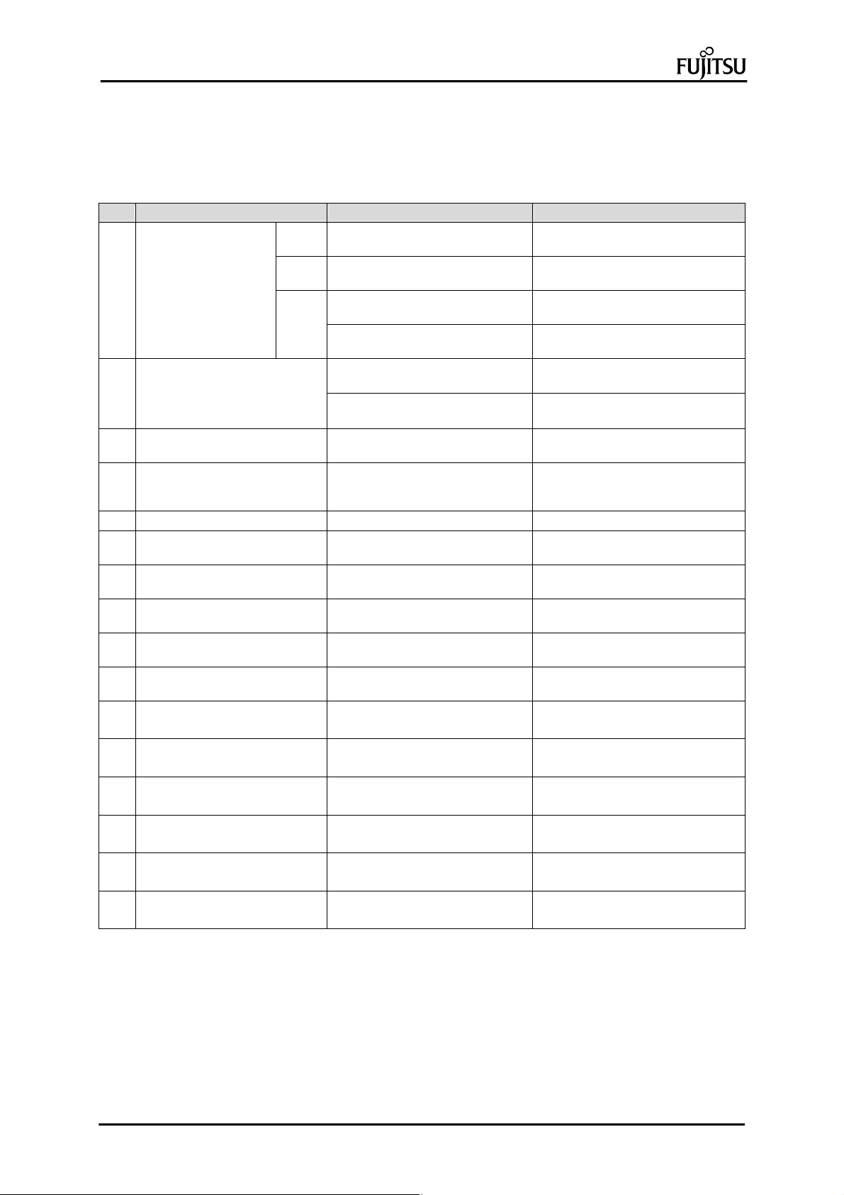
The table below shows the general specifications.
Table 1-1 General specifications
No. Item Contents Remarks
CPU board
1 Board name
Base board
Option board
DDR2
Flash ROM
Display I/F
Capture I/F
Ethernet I/F
I2S I/F
MLB I/F
CAN I/F
LIN (USART) / UART I/F
SD I/F
USB I/F
PWM I/F
GPIO I/F
2 Function
IrDA I/F
IDE I/F
TS I/F
JTAG I/F
TRACE I/F
I2C I/F
A/D I/F
TCON
Quad-SPI
SFI
External Bus
DMA REQ
External INT
SW
LED
Operating ambient
3
temperature
4 Storage temperature 0 to 70°C
5 Humidity Normal humidity No condensation
6 Environment friendly Conforming product
7 Power supply AC adaptor input +12V 5A or less
Normal temperature
CPU board
W H = 127mm 117.5mm
8 Board dimensions
Base board
W H = 330mm 222.5mm
Option board
W H = 222.5mm 105mm
2
1. Outline of MB86R11EVB
Page 9
MB86R11
MB86R11EVB Hardware Manual
Evaluation Board
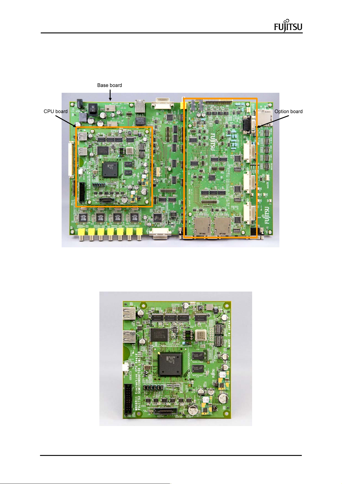
1.3. External view
The external view of MB86R11EVB is shown as follows.
Figure 1-1 External view of MB86R11EVB
External view of CPU board
Figure 1-2 External view of CPU board
3
1. Outline of MB86R11EVB
Page 10
MB86R11
MB86R11EVB Hardware Manual
Evaluation Board
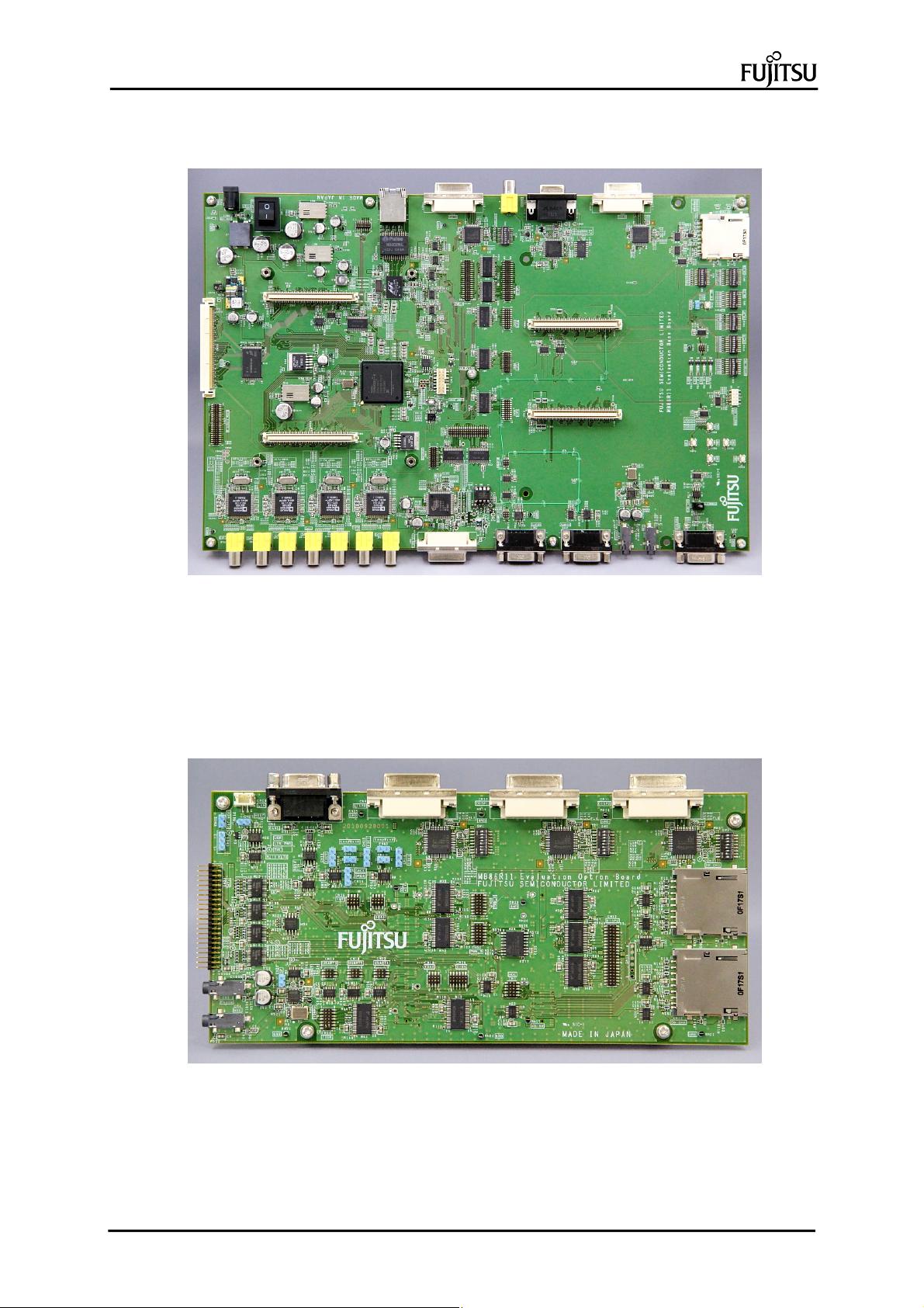
External view of Base board
Figure 1-3 External view of Base board
External view of Option board
Figure 1-4 External view of Option board
4
1. Outline of MB86R11EVB
Page 11
MB86R11
MB86R11EVB Hardware Manual
Evaluation Board
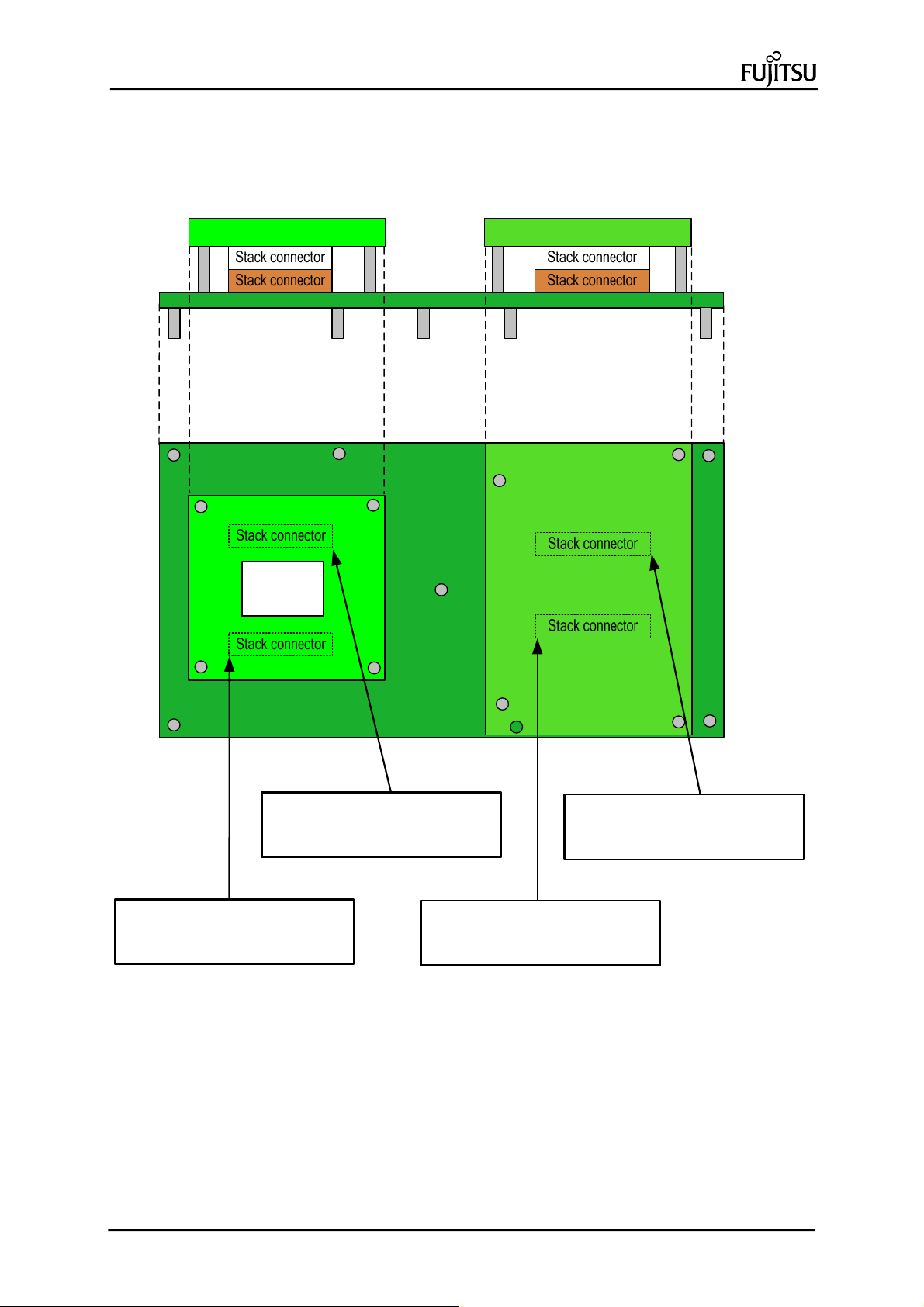
1.4. Connection configuration
The connection configuration is shown as follows.
CPU Board Option Board
A
Base Board
MB86R1
1
Option Board
B
Base Board
CPU Board
A
CPUboard side connector CN8
Base board side connector
CPU board side connector CN9
Base board side connector
CN32
Figure 1-5 Connection configuration of MB86R11EVB
CN31
Option board side connector
Base board side connector
Option board side connector
CN7
Base board side connector
CN33
B
CN8
CN34
5
1. Outline of MB86R11EVB
Page 12
MB86R11
MB86R11EVB Hardware Manual
Evaluation Board
2. Outline of Hardware
This chapter describes the outline of hardware of MB86R11EVB.
2.1. Hardware specifications of CPU board
Table 2-1 shows the hardware specifications of CPU board.
Table 2-1 Hardware specifications of CPU board
Used CPU
1 MB86R11 PBGA-544pin
Installed function
No. Item Contents Remarks
1 DDR2
2 NOR-FLASH
3 USB-Host 292303-1 (Tyco) USB-A connector
USB-Host 292303-1 (Tyco)
4
USB-Function UX60SC-MB-5ST (HRS)
5 ICE PS-20PE-D4T1-B1 (JAE) JTAG connector
6 TRACE 2-5767004-2 (Tyco) ETM connector
7 Base board connection
MT47H64M16HR-25E_IT (Micron) 2
1Gbit (64M×16bit) 2
JS28F512M29EWL (Numonyx) 2
512Mbit (32Mword 16bit) 2
53647-1674 (Molex) 2
This is a composition when 32bit bus is
connected.
When boot from NOR-FLASH is used, it
becomes a composition of 512Mbit 1 because
the bus is fixed to 16bit.
USB-A connector
(Exclusive use with USB-Function)
Mini-B connector
(Exclusive use with USB-Host)
160pin stack
6
2. Outline of Hardware
Page 13
MB86R11
MB86R11EVB Hardware Manual
Evaluation Board
2.2. Hardware specifications of Base board
Table 2-2 shows the hardware specifications of Base board.
Table 2-2 Hardware specifications of Base board (1/2)
Used FPGA
1 Spartan6 XC6SLX100-2FGG676C (Xilinx) FBGA-676pin
No. Item Contents Remarks
The connector is DVI-I.
SiI164BCT64 (Silicon Image)
1.27mm pitch
1.27mm pitch
The connector is DVI-I.
SiI164BCT64 (Silicon Image)
1.27mm pitch
SiI1161CT (Silicon Image)
The connector is DVI-I.
1.27mm pitch
1.27mm pitch
1.27mm pitch
1.27mm pitch
GbE-PHY
88E1111-B2-BAB-C000 (Marvell)
OUTPUT
INPUT
2.0mm pitch
1.27mm pitch
Diplay0
1 Display (2ch)
Display1
Capture0
Capture (4ch)
2
Capture1
3 Ethernet
4 I2S (CH0: AUDIO)
5 MediaLB
6 CAN (CH0)
7 USART/UART (CH0, CH1)
8 SD (CH0)
DVI-D
CVBS ADV7343BSTZ (Analog devices)
Analog RGB ADV7343BSTZ (Analog devices)
RSDS (Header pin)
OQW-11-4.2-20PW (Mac8)
External output (Header pin)
OQW-11-4.2-20PW (Mac8)
DVI-D
External output (Header pin)
OQW-11-4.2-20PW (Mac8)
DVI-D
CVBS (YUV) ADV7403KSTZ (Analog devices)
External input (Header pin)
OQW-11-4.2-20PW (Mac8)
CVBS (YUV) ADV7403KSTZ (Analog devices)
Video Component (720P) ADV7403KSTZ (Analog devices)
External input (Header pin)
OQW-11-4.2-10PW (Mac8)
CVBS (YUV) ADV7403KSTZ (Analog devices)
External input (Header pin)
OQW-11-4.2-10PW (Mac8)
CVBS (YUV) ADV7403KSTZ (Analog devices)
External input (Header pin)
OQW-11-4.2-10PW (Mac8)
RJ45 connector
TM21R-5C-88 (HRS)
Stereo mini Jack 1
STX-3500-4N (Kycon)
Stereo mini Jack 1
STX-3500-4N (Kycon)
Connector for evaluation (Header pin)
A3A-10PA-2SV (71) (Hirose)
D-sub9
RDED-9P-LNA (4-40) (55)
(HONDA TSUSHIN)
D-sub9
RDED-9P-LNA (4-40) (55)
(HONDA TSUSHIN)
External input/output (Header pin)
OQW-11-4.2-03PW (Mac8)
SD card slot
DM1AA-SF-PEJ(HRS)
7
2. Outline of Hardware
Page 14
MB86R11
MB86R11EVB Hardware Manual
Evaluation Board
Table 2-2 Hardware specifications of Base board (2/2)
No. Item Contents Remarks
LED for power supply (Green)
LED 1 SML-310MT (ROHM)
9 LED
CH11-14
10
GPIO 10
CH5-10
11 TS
12 I2C (CH0, CH1) For setting of IC
13 EEPROM
INT_A0
14 External INT
INT_A1
15 NAND FLASH
FPGA
16
configuration
17 CPU board connection
18 Option board connection
Customer board connection
19
connector
20 MB86R11 mode selection switch
21 Capture input selection switch
JTAG 98424-G52-14ALF (FCI) For FPGA writing
Config-ROM S25FL032P0XMFI011 (SPANSION) Quad SPI
LED for FPGA reset (Green)
LED 1 SML-310MT (ROHM)
LED for configuration (Green)
LED 1 SML-310MT (ROHM)
LED 4
SML-310MT (ROHM)
External input/output (Header pin)
OQW-11-4.2-03PW (Mac8)
SW 6
SKRPABE010 (ALPS ELECTRIC)
External pin (Header pin)
OQW-11-4.2-07PW (Mac8)
BR25S256F (ROHM)
256Kbit
SW 1
SKRPABE010 (ALPS ELECTRI)
External input (Header pin)
FFC-03ASM1 (HONDA TSUSHI)
External input (Header pin)
FFC-03ASM1 (HONDA TSUSHI)
MT29F2G08ABAEAWP (Micron)
2Gbit (8bit Bus)
52837-1679 (Molex) 2
52837-1679 (Molex) 2
87BFN100R-3F (KEL) 100pin right angle
8bit slide switch 4
CHS-08B (NIDEC COPAL
ELECTRONICS)
8bit slide switch
CHS-08B (NIDEC COPAL
ELECTRONICS)
It lights when SW17 is turned on when
the power is supplied to the Base board.
It lights when FPGA is reset.
It lights when the FPGA configuration is
completed.
Green LED
Tact switch
1.27mm pitch
Tact switch
2.54mm pitch
2.54mm pitch
160pin stack
160pin stack
8
2. Outline of Hardware
Page 15
MB86R11
MB86R11EVB Hardware Manual
Evaluation Board
2.3. Hardware specifications of Option board
Table 2-3 shows the hardware specifications of Option board.
Table 2-3 Hardware specifications of Option board
No. Item Contents Remarks
Diplay0 DVI-D
Diplay1 DVI-D
1 Display (3ch)
DVI-D
Diplay2
2 I2S (CH1)
3 I2S (CH2, CH3)
4 CAN (CH1)
5 LIN (USART)/UART (CH5) B2B-PH-SM4-TB (JST)
6
SD 2 (CH1, CH2)
7
PWM 12
8 IrDA
9
I2C (CH2~4)
10 General-purpose ADC
11 TCON
12 SPI-FLASH (Quad)
13 SPI-FLASH (Single)
14 External INT (CH2)
15 DMA REQ
16 IDE
External output (Header pin)
OQW-11-4.2-20PW (Mac8)
OUT: Stereo mini Jack 1
STX-3500-4N (Kycon)
IN: Stereo mini Jack 1
STX-3500-4N (Kycon)
External input/output (Header pin)
OQW-11-4.2-04PW (Mac8)
D-sub9
RDED-9P-LNA (4-40) (55)
(HONDA TSUSHIN)
SD card slot
DM1AA-SF-PEJ (HRS)
External output (Header pin)
OQW-11-4.2-07PW (Mac8)
External input/output (Header pin)
OQW-11-4.2-06PW (Mac8)
External input/output (Header pin)
FFC-03ASM1 (HONDA TSUSHIN)
External input/output (Header pin)
OQW-11-4.2-05PW (Mac8)
External output (Header pin)
OQW-11-4.2-07PW (Mac8)
S25FL064P0XMFI001 (Spansion)
64Mbit
W25Q32BVSSIG (Winbond)
32Mbit
External input (Header pin)
OQW-11-4.2-04PW (Mac8)
External input/output (Header pin)
FFC-03ASM1 (HONDA TSUSHIN)
External input/output (Header pin)
WCAW-20-2-22PW (Mac8)
The connector is DVI-I.
SiI164BCT64(Silicon Image)
The connector is DVI-I.
SiI164BCT64(Silicon Image)
The connector is DVI-I.
SiI164BCT64(Silicon Image)
1.27mm pitch
1.27mm pitch
1.27mm pitch
1.27mm pitch
2.54mm pitch
1.27mm pitch
1.27mm pitch
1.27mm pitch
2.54mm pitch
9
2. Outline of Hardware
Page 16
MB86R11
Evaluation Board
MB86R11EVB Hardware Manual
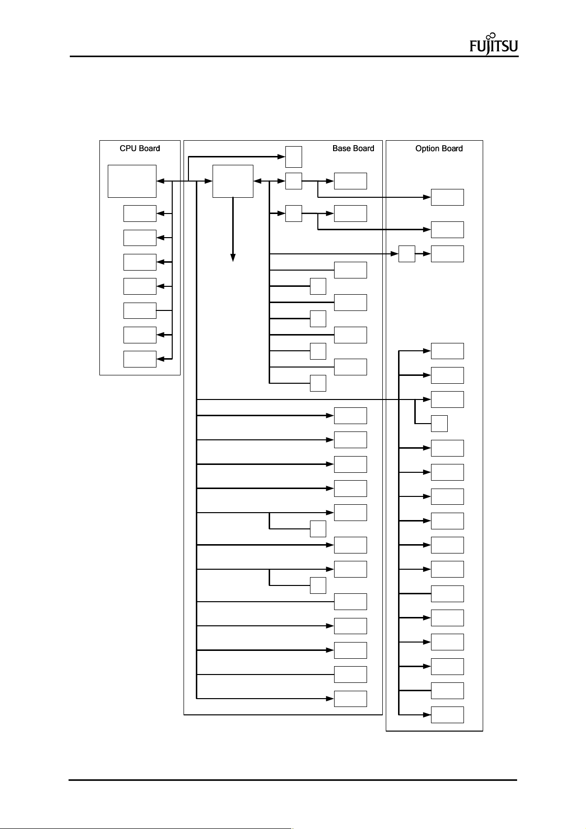
2.4. Block diagram
Figure 2-1 shows the block diagram of MB86R11EVB.
MB86R11 FPGA
DDR2
Nor Flash
USB-
Host
USB-
Host
USB-
Function
ICE
TRACE
Enable signal of
each buffer
PIN
(RSDS)
PIN
PIN
PIN
PIN
PINPIN
DISP0
DISP1
CAP0
CAP1
CAP2
CAP3
Ethernet
AUDIO
MLB
CAN
USART
SD Card
DISP0
DISP1
PIN
DISP2
LIN
IDE
AUDIO
PIN
CAN
USART
SD Card
PWM
IrDA
PINPIN
GPIO
TS
I2C
EEPROM
INT
NAND
Flash
I2C
A/D
TCON
Quad SPI
SPI Flash
INT
DMA REQ
Figure 2-1 Block diagram of MB 86 R 11EVB
10
2. Outline of Hardware
Page 17
MB86R11
MB86R11EVB Hardware Manual
Evaluation Board
3. Details of hardware
This chapter describes details of the hardware of MB86R11EVB.
3.1. CPU board
Single-chip system LSI MB86R11 with built-in CoreTex-A9 is used for CPU.
Table 3-1 CPU
No. Item Model number Manufacturer Quantity Remarks
1 CPU MB86R11 Fujitsu Semiconductor 1 PBGA544pin
3.1.1. External Bus
NOR-FLASH of 1Gbit (512Mbit) is connected to External Bus of CPU board.
Table 3-2 NOR-FLASH
No. Item Model number Manufacturer Quantity Remarks
1 NOR-FLASH JS28F512M29EWL Numonyx 2 128MB
(32Mword×16bit×2)
3.1.2. DDR2
The CPU board has 2Gbit (1Gbit 2) as DDR2 interface.
It is a composition in which 4Gbit (2Gbit 2) can be connected.
Table 3-3 DDR2
No. Item Model number Manufacturer Quantity Remarks
1 DDR2 MT47H64M16HR-25E_IT MICRON 2 256MB
(64Mb 16bit 2)
3.1.3. USB-Host
The CPU board has the USB2.0-Host by 2 ports (CN3 and CN5).
The CN3 is exclusively used with Function (CN4).
Table 3-4 USB-Host
No. Item Model number Manufacturer Quantity Remarks
1 USB connector 292303-1 Tyco 2 TypeA
2 High side switch TPS2061D TI 1 Power supply control
3 Crystal oscillator MXO3-7050 48MHz MITADENPA 1 48MHz/50ppm
All USB ports
11
3. Details of hardware
Page 18
MB86R11
MB86R11EVB Hardware Manual
Evaluation Board
3.1.4. USB-Function
The CPU board has the USB2.0-Function by 1 port (CN4).
VBUS is connected to INT_A[1].
Table 3-5 USB-Function
No. Item Model number Manufacturer Quantity Remarks
1 USB connector UX60SC-MB-5ST HRS 1 miniB
2 Schmitt buffer SN74LVC1G17DCK TI 1 VBUS detection
3 Crystal oscillator MXO3-7050 48MHz MITADENPA 1 48MHz/50ppm
All USB ports
3.1.5. ARM JTAG/ETM
The CPU board has JTAG (CN1) and the ETM connector (CN2) for the ARM debugging.
Enable ETM probe (HLX600TP) and JTAG cable (HLX600JP) of YDC AdviceLUNA to be connected.
Table 3-6 ARM JT A G/ E T M
No. Item Model number Manufacturer Quantity Remarks
1 JTAG PS-20PE-D4T-B1 JAE 1
2 ETM 2-5767004-2 Tyco 1
2列20極
2列38極
12
3. Details of hardware
Page 19
MB86R11
MB86R11EVB Hardware Manual
Evaluation Board
3.1.6. Selection of boot flash memory
The CPU board has the switch that selects the boot memory. It can select either of NOR-FLASH or
NAND-FLASH of the external memory.
Table 3-7 Slide switch
No. Item Model number Manufacturer Quantity Remarks
1 Slide switch MAS-D20A1 Fujisoku 1
SW1 (Selection of boot memory type)
MB86R11
NAND-FLASH
Table 3-8 SW1 setting
SW1 Boot memory type Remarks
MB86R11 side NAND-FLASH
The other side NOR-FLASH (Default) Default
NOR-FLASH
Cannot used
13
3. Details of hardware
Page 20
MB86R11
MB86R11EVB Hardware Manual
Evaluation Board
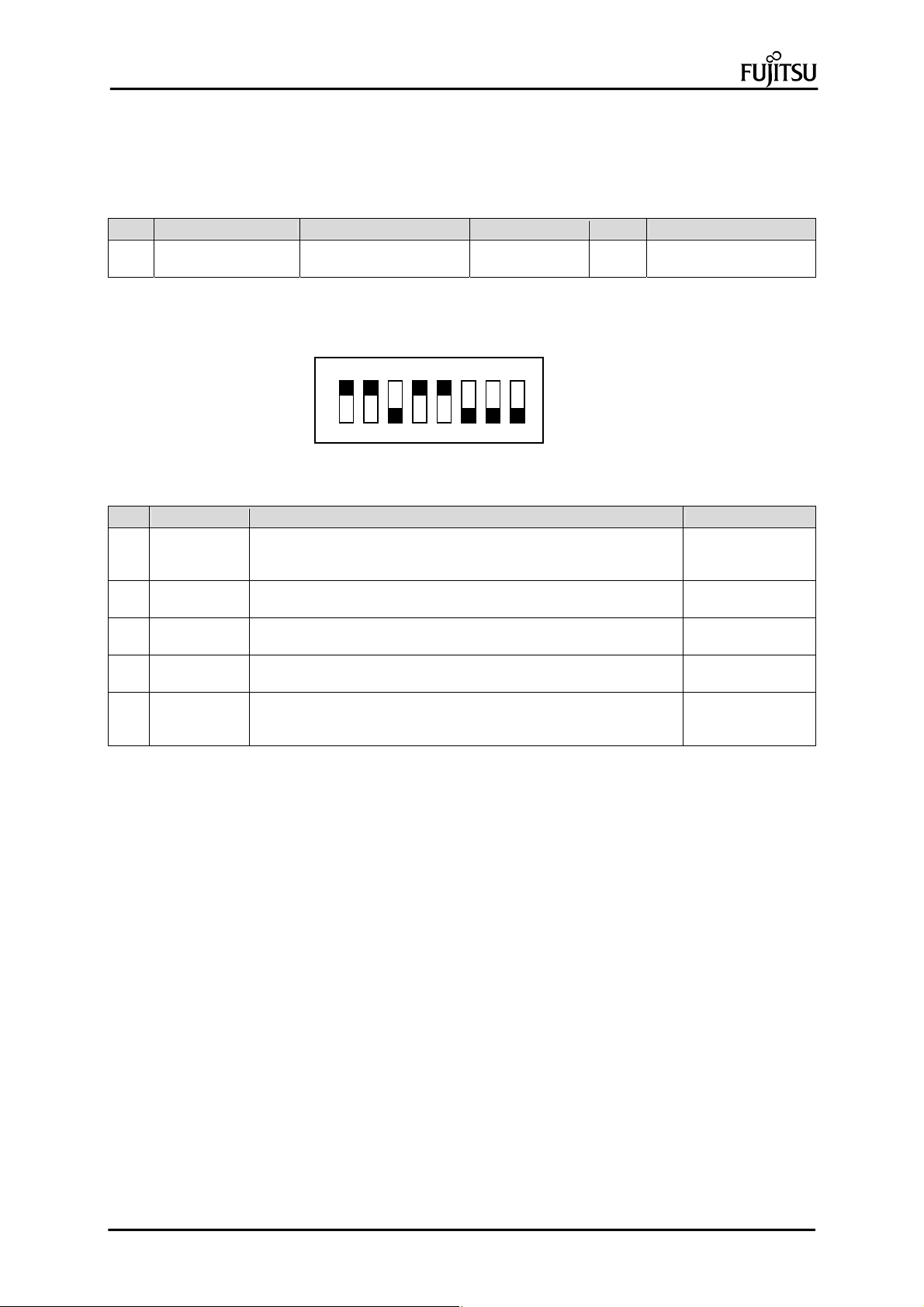
3.1.7. Pin Multiplex Switch
The setting of each switch on CPU board is as follows.
Table 3-9 DIP SW
No. Item Model numbe r Manufacturer Quantity Remarks
1 DIP SW CHS-08B NIDEC COPAL
ELECTRONICS
SW2 (PLLMODE)
8 1
2
ON
Default
Table 3-10 SW2 setting
SW2 Signal Description Default
4:1 CRIPM[3:0] ON=0, OFF=1
SW[4, 3, 2, 1]=[ON, ON, ON, ON]=0000
SW[4, 3, 2, 1]=[OFF, OFF, OFF, OFF]=1111
5 PLLBYPASS OFF=PLL clock is not bypassed.
ON=PLL clock is bypassed.
6 PSMODE ON=PSMODE are reflected to the PLL clock frequency.
OFF=PSMODE are not reflected to the PLL clock frequency
7 VINTHI ON=The exception vectors are located at 0xFFFF_0000.
OFF=The exception vectors are located at 0x0000_0000.
8 USB_S Use USB-Host (CN3) / USB-Function
ON=USB-Host (CN3)
OFF=USB-Function (CN4)
SW[4, 3, 2, 1]=
[OFF, ON, ON, ON]
OFF
ON
OFF
OFF
14
3. Details of hardware
Page 21
MB86R11
t
MB86R11EVB Hardware Manual
Evaluation Board
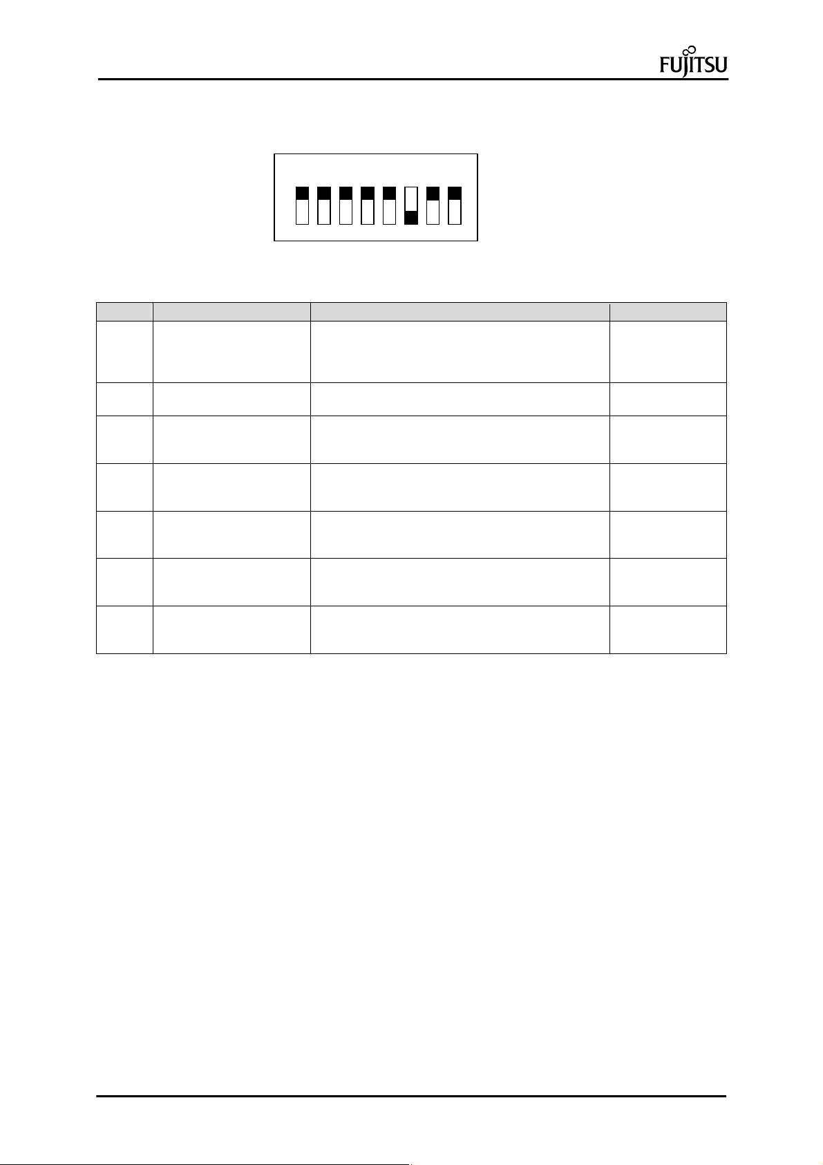
SW3 (MPXMODE)
Table 3-11 SW3 setting
SW3 Signal Description Default
2:1 MPXMODE[1:0] SW[2:1]=[OFF, OFF]=Mode0
3 MPXMODE[2] OFF=Mode0
4 NOR_EAEN NOR-FLASH bus select
5 JTAGSEL JTAG select
6 TEST MODE TEST mode
7 TRACEEN0 Pin Group B ETM
8 TRACEEN1 Pin Group H ETM
8 1
ON
SW[2:1]=[OFF, ON]=Mode1
SW[2:1]=[ON, ON]=Mode1
SW[2:1]=[ON, OFF]=Mode2
ON=Mode2
ON=32bit
OFF=16bit
OFF= Normal
ON=DFT
OFF= Normal
ON= TEST mode
ON=Used
OFF=Unused
ON= Used
OFF= Unused
Defaul
SW[2, 1]=
[OFF, OFF]
ON
OFF
OFF
OFF
OFF
OFF
15
3. Details of hardware
Page 22
MB86R11
MB86R11EVB Hardware Manual
Evaluation Board
3.1.8. Jumper setting
The CPU board has the header pin that has the following functions.
Table 3-12 General-purpose pin header
No. Item Model number Manufacturer Quantity Remarks
1 General-purpose pin
header
Table 3-13 Jumper setting
CN Function Description Default
10 OSC Open (Fixed) Open
11 VRH0 Short= ADC is not used.
12 VRH1 Short= ADC is not used.
13 VRL0 Short= ADC is not used.
14 VRL1 Short= ADC is not used.
15 VIN0 Short= ADC is not used.
16 VIN1 Short= ADC is not used.
Note:
CN11-16 must "OPEN" when the ADC connector of the Option board is used.
FFC-2ASM1 HONDA TSUSHIN 7 1 row, 2 poles
Short
Open= ADC is used.
Open= ADC is used.
Open= ADC is used.
Open= ADC is used.
Open= ADC is used.
Open= ADC is used.
Short
Short
Short
Short
Short
16
3. Details of hardware
Page 23
MB86R11
MB86R11EVB Hardware Manual
Evaluation Board
3.2. Base board
The AC adaptor is connected to this board, and it supplies power to each board.
The signal of the Display, Capture, and External Bus are connected to FPGA, and an enable control is
performed for the buffer of each resource according to the mode that the user set.
3.2.1. FPGA
The FPGA of the Base board provides a selector function of Display and Capture and a buffer enable
control functions of each resource.
External Bus connects the following signals with FPGA:
lower 10 bits of address (A[11:1])
32 bits control signal (excluding the signal for NAND) of data
Table 3-14 FPGA
No. Item Model number Manufacturer Quantity Remarks
1 FPGA XC6SLX100-2FGG676C Xilinx 1 Spartan6
2 Writing connector 98424-G52-14ALF FCI 1 2 rows, 14 poles
3 Configuration ROM S25FL032P0XMFI011 SPANSION 1 32Mbit
3.2.2. External Bus
The 256MB NAND-FLASH is connected to External Bus of the Base board.
To connect External Bus signals with customer's board, they are connected to the connector.
Refer to "4.3 Customer I/F" for detail.
Table 3-15 External Bus
No. Item Model number Manufacturer Quantity Remarks
1 NAND-FLASH MT29F2G08ABAEAWP MICRON 1
256MB (8bit×256Mbit)
17
3. Details of hardware
Page 24

MB86R11
MB86R11EVB Hardware Manual
Evaluation Board
3.2.3. Display
The Base board has 2 ports (Display0 and Display1) as an image output interface, and is output with the
DVI connector. In addition, only the Diplay0 port has CVBS and the analog RGB connector for the analog
output.
The pin header of Display is described below.
Table 3-16 Display
No. Item Model number Manufacturer Quantity Remarks
1 DVI transmitter SiI164BCT64 SiliconImage 2
2 DVI-I connector 1734148-1 Tyco 2
3 Video DAC ADV7343 AnalogDevices 1
4 AnalogRGB connector 1-1734570-1 Tyco 1 Dsub15
5 NTSC connector LPR6520-0804F SMK 1
6 Display Header pins I/F OQW-11-4.2-20PW Mac8 2 2 rows, 40 poles
1.27mm pitch
(Remark) DISP0 connector DVI-I=CN1, CVBS=CN4, RGB=CN3,Header pin=CN20
DISP1 connector DVI-I=CN2,Header pin=CN27
Figure 3-1 Display circuit
18
3. Details of hardware
Page 25
MB86R11
MB86R11EVB Hardware Manual
Evaluation Board
Table 3-17 Capture (CH0) pin assignment
No. Signal name I/O Description No. Signal name I/O Description
1 GND - Ground 21 GND - Ground
2 GND - Ground 22 GND - Ground
3 B0 I 23 HD I
4 B1 I 24 VD I
5 B2 I 25 DE I
6 B3 I 26 - -
7 B4 I 27 GND - Ground
8 B5 I 28 GND - Ground
9 B6 I 29 R0 I
10 B7 I 30 R1 I
11 GND - Ground 31 R2 I
12 GND - Ground 32 R3 I
13 G0 I 33 R4 I
14 G1 I 34 R5 I
15 G2 I 35 R6 I
16 G3 I 36 R7 I
17 G4 I 37 GND - Ground
18 G5 I 38 GND - Ground
19 G6 I 39 CLK I
20 G7 I 40 GND - Ground
(Remark) The physical pin assignment is the same as the audio general-purpose pin header.
Table 3-18 Capture YUV (CH0, CH1, CH 2, CH3) pin assignment
No. Signal name I/O Description No. Signal name I/O Description
1 V0 I 2 GND - Ground
3 V1 I 4 GND - Ground
5 V2 I 6 GND - Ground
7 V3 I 8 GND - Ground
9 V4 I 10 GND - Ground
11 V5 I 12 GND - Ground
13 V6 I 14 GND - Ground
15 V7 I 16 GND - Ground
17 CLK I 18 GND - Ground
19 - - 20 GND - Ground
(Remark) The physical pin assignment is the same as the audio general-purpose pin header.
19
3. Details of hardware
Page 26

MB86R11
t
MB86R11EVB Hardware Manual
Evaluation Board
SW1 (DISP0_DAC_CTRL)
8 1
Set SW1[2:1]=[OFF, OFF] when I2C0 is used.
SW1 Signal Description
1 DSEL
2 BSEL
3 EDGE
HTPLG
Dual edge clock select / I2C Data
/
SDA
/
SCL
/
This pin is an open collector input/output.
If I2C bus is enabled (ISEL=OFF), then this pin is the I2C data line.
If the I2C bus is disabled (ISEL=ON), then this pin selects whether single clock
dual edge is used.
Dual Edge clock select:
DSEL=OFF:
IDCK+ latches input data on both falling and rising clock edges.
DSEL=ON:
IDCK+/IDCK- latches input data on only falling or rising clock edges.
In 24-/12-bit mode:
DSEL=OFF (dual edge):
IDCK+ is used to latch data on both falling and rising edges.
DSEL=ON (single edge):
IDCK+ latches 1st half data and IDCK- latches 2nd half data.
Input bus select / I2C clock.
This pin is an open collector input.
If I2C bus is enabled (ISEL=OFF), then this pin is the I2C clock input.
If the I2C is disabled (ISEL=ON), then this pin selects the input bus width.
Input Bus Select:
BSEL=OFF:
selects 24-bit input mode
BSEL=ON:
selects 12-bit input mode
Edge select / Hot Plug input.
If the I2C bus is enabled (ISEL=OFF), then this pin is used to monitor the "Hot
Plug" detect signal (Please refer to the DVI or VESA P&D and DFP standards).
This Input is ONLY 3.3V tolerant and has no internal de-bouncer circuit.
If I2C bus is disabled (ISEL=ON), then this pin selects the clock edge that will
latch the data. How the EDGE setting works depends on whether dual or single
edge latching is selected.
Dual Edge Mode (DSEL = OFF)
EDGE=ON:
the primary edge (first latch edge after DE is asserted) is the falling edge.
EDGE=OFF:
the primary edge (first latch edge after DE is asserted) is the rising edge.
(Note) In 24-bit Single Clock Dual Edge mode, EDGE is ignored.
Single Edge Mode (DSEL=ON)
EDGE=ON:
the falling edge of the clock is used to latch data.
EDGE=OFF:
the rising edge of the clock is used to latch data.
ON
Defaul
Default
(I2C mode)
OFF
OFF
OFF
20
3. Details of hardware
Page 27

MB86R11
MB86R11EVB Hardware Manual
Evaluation Board
SW1 Signal Description
4 DKEN
7:5 CTL[1:3]
A[1:3]
DK[1:3]
8 ISEL
Refer to the data sheet of SiI164BCT64 for detail.
/
/
/
RST#
De-skewing enable.
I2C mode (ISEL=OFF)
DKEN pin must be set to OFF.
DK[3:1] pins are ignored and the De-skewing increments are selected through
the I2C interface.
Non I2C mode (ISEL=ON)
DKEN=ON:
then default De-skewing setting is used.
DKEN=OFF:
then DK[3:1] is used as the De-skewing setting.
The use of these multi-function inputs depends on the settings of ISEL and DKEN.
ISEL=ON, DKEN=ON:
General-Purpose Input CTL[1:3] pins are active, for backward compatibility.
These pins must be used to send DC signals only during the blanking time.
ISEL=ON, DKEN=OFF
DK[1:3] are active, these inputs are used to select the De-skewing setting for the
input bus.
ISEL=OFF, DKEN=OFF
A[1:3] are active, these bits are used to set the lower 3 bits of the I2C device
address.
I2C Interface Select.
ISEL=OFF:
I2C interface is active.
ISEL=ON:
I2C is inactive and the chip configuration is read from the configuration
strapping pins.
This pin also acts as an asynchronous reset to the I2C interface controller.
(Note) When the I2C interface is active, DKEN must be set OFF.
Default
(I2C mode)
OFF
SW[7, 6, 5]
=A[1, 2, 3]
=[OFF, OFF, OFF]
I2C device address:
0111, A3, A2, A1
=0111000 (*1)
*1) ON="1", OFF="0"
OFF
21
3. Details of hardware
Page 28

MB86R11
t
MB86R11EVB Hardware Manual
Evaluation Board
SW2 (DISP_DAC_CTRL1)
Set SW2[2:1]=[OFF, OFF] when I2C0 is used.
SW2 Signal Description
1 DSEL
2 BSEL
3 EDGE
HTPLG
Dual edge clock select / I2C Data
/
SDA
/
SCL
/
This pin is an open collector input/output.
If I2C bus is enabled (ISEL=OFF), then this pin is the I2C data line.
If the I2C bus is disabled (ISEL=ON), then this pin selects whether single clock
dual edge is used.
Dual Edge clock select:
DSEL=OFF:
IDCK+ latches input data on both falling and rising clock edges.
DSEL=ON:
IDCK+/IDCK- latches input data on only falling or rising clock edges.
In 24-/12-bit mode:
DSEL=OFF (dual edge):
IDCK+ is used to latch data on both falling and rising edges.
DSEL=ON (single edge):
IDCK+ latches 1st half data and IDCK- latches 2nd half data.
Input bus select / I2C clock.
This pin is an open collector input.
If I2C bus is enabled (ISEL=OFF), then this pin is the I2C clock input.
If the I2C is disabled (ISEL=ON), then this pin selects the input bus width.
Input Bus Select:
BSEL=OFF:
selects 24-bit input mode
BSEL=ON:
selects 12-bit input mode
Edge select / Hot Plug input.
If the I2C bus is enabled (ISEL=OFF), then this pin is used to monitor the "Hot
Plug" detect signal (Please refer to the DVI or VESA P&D and DFP standards).
This Input is ONLY 3.3V tolerant and has no internal de-bouncer circuit.
If I2C bus is disabled (ISEL=ON), then this pin selects the clock edge that will
latch the data. How the EDGE setting works depends on whether dual or single
edge latching is selected.
Dual Edge Mode (DSEL = OFF)
EDGE=ON:
the primary edge (first latch edge after DE is asserted) is the falling edge.
EDGE=OFF:
the primary edge (first latch edge after DE is asserted) is the rising edge.
(Note) In 24-bit Single Clock Dual Edge mode, EDGE is ignored.
Single Edge Mode (DSEL=ON)
EDGE=ON:
the falling edge of the clock is used to latch data.
EDGE=OFF:
the rising edge of the clock is used to latch data.
ON
Defaul
Default
(I2C mode)
OFF
OFF
OFF
22
3. Details of hardware
Page 29

MB86R11
MB86R11EVB Hardware Manual
Evaluation Board
SW2 Signal Description
4 DKEN
7:5 CTL[1:3]
A[1:3]
DK[1:3]
8 ISEL
Refer to the data sheet of SiI164BCT64 for detail.
/
/
/
RST#
De-skewing enable.
I2C mode (ISEL=OFF)
DKEN pin must be set to OFF.
DK[3:1] pins are ignored and the De-skewing increments are selected through
the I2C interface.
Non I2C mode (ISEL=ON)
DKEN=ON:
then default De-skewing setting is used.
DKEN=OFF:
then DK[3:1] is used as the De-skewing setting.
The use of these multi-function inputs depends on the settings of ISEL and DKEN.
ISEL=ON, DKEN=ON:
General-Purpose Input CTL[1:3] pins are active, for backward compatibility.
These pins must be used to send DC signals only during the blanking time.
ISEL=ON, DKEN=OFF
DK[1:3] are active, these inputs are used to select the De-skewing setting for the
input bus.
ISEL=OFF, DKEN=OFF
A[1:3] are active, these bits are used to set the lower 3 bits of the I2C device
address.
I2C Interface Select.
ISEL=OFF:
I2C interface is active.
ISEL=ON:
I2C is inactive and the chip configuration is read from the configuration
strapping pins.
This pin also acts as an asynchronous reset to the I2C interface controller.
(Note) When the I2C interface is active, DKEN must be set OFF.
Default
(I2C mode)
OFF
SW[7,6,5]
=A[1, 2, 3]
=[ON, OFF, OFF]
I2C device address:
0111, A3, A2, A1
=0111001 (*1)
*1) ON="1", OFF="0"
OFF
23
3. Details of hardware
Page 30

MB86R11
Evaluation Board
MB86R11EVB Hardware Manual
3.2.4. Capture
The Base board has 4 ports as an image output interface.
Capture0 can be input from DVI, NTSC, and the pin header, and Capture1 can be input from HD, NTSC,
and the pin header.
Capture2/3 can be input from NTSC and the pin header.The pin header of Capture is described below.
Table 3-19 Capture
No. Item Model number Manufacturer Quantity Remarks
1 Video decoder ADV7403 AnalogDevices 4
2 Crystal oscillator MXO3-5032 28.63636MHz MITADENPA 1 28.63636MHz/50ppm
3 NTSC connector LPR6520-0804F SMK 4
4 HD connector LPR6520-0804F SMK 3
5 DVI receiver SiI1161 SiliconImage 1
6 DVI-I connector 1734148-1 Tyco 1
7 EEPROM 24LC21A/P Microchip
Technology
8
9
(Remark) Capture0 connector DVI-I=CN5, NTSC=CN6,Header pin=CN35
Capture1 connector HD=CN39~CN41, NTSC=CN8,Header pin=CN28
Capture2 connector NTSC=CN9,Header pin=CN29
Capture3 connector NTSC=CN10,Header pin=CN30
1 Socket mounting
3.3V
R
PD#
Sil1161
ADV7403
ADV7403
ADV7403
I2C0
I2C0
I2C1
3.3V
R
OE#
SW1=L & SW2=L : H
3.3V
R
OE#
SW1=L & SW2=H : H
3.3V
R
OE#
3.3V
R
OE#
3.3V
R
OE#
3.3V
R
OE#
SW1
CAP0
3.3V
R
SW2
CAP1
SW3
Circuit x 2
CAP2/3
SW4/5
Figure 3-2 Capture input path select circuit
24
3. Details of hardware
Page 31

MB86R11
MB86R11EVB Hardware Manual
Evaluation Board
Table 3-20 Capture (CH0) pin assignment
No. Signal name I/O Description No. Signal name I/O Description
1 GND - Ground 21 GND - Ground
2 GND - Ground 22 GND - Ground
3 B0 I 23 HD I
4 B1 I 24 VD I
5 B2 I 25 DE I
6 B3 I 26 - -
7 B4 I 27 GND - Ground
8 B5 I 28 GND - Ground
9 B6 I 29 R0 I
10 B7 I 30 R1 I
11 GND - Ground 31 R2 I
12 GND - Ground 32 R3 I
13 G0 I 33 R4 I
14 G1 I 34 R5 I
15 G2 I 35 R6 I
16 G3 I 36 R7 I
17 G4 I 37 GND - Ground
18 G5 I 38 GND - Ground
19 G6 I 39 CLK I
20 G7 I 40 GND - Ground
(Remark) The physical pin assignment is the same as the audio general-purpose pin header.
Table 3-21 Capture YUV (CH0, CH1, CH 2, CH3) pin assignment
No. Signal name I/O Description No. Signal name I/O Description
1 V0 I 2 GND - Ground
3 V1 I 4 GND - Ground
5 V2 I 6 GND - Ground
7 V3 I 8 GND - Ground
9 V4 I 10 GND - Ground
11 V5 I 12 GND - Ground
13 V6 I 14 GND - Ground
15 V7 I 16 GND - Ground
17 CLK I 18 GND - Ground
19 - - 20 GND - Ground
(Remark) The physical pin assignment is the same as the audio general-purpose pin header.
25
3. Details of hardware
Page 32

MB86R11
MB86R11EVB Hardware Manual
Evaluation Board
3.2.5. Ethernet
The Base board has 1 port (CN11) as the Ethernet interface for GbE.
Table 3-22 GbE
No. Item Model numbe r Manufacturer Quantity Remarks
1 GbE-PHY 88E1111-B2-BAB-C000 Marvell 1
2 LAN connector TM21R-5C88(50) HRS 1
3 Transformer H5007NL Pulse 1
4 Xtal CX-8045G 25MHz KYOCERA 1 25MHz
3.2.6. EEPROM
The EEPROM is connected to SPI0 of the Base board.
Table 3-23 EEPROM
No. Item Model number Manufacturer Quantity Remarks
1 EEPROM BR25S256F ROHM 1 256Kbit
3.2.7. I2S (AUDIO)
As for the Base board, I2C0 1ch is connected to the audio device as the audio interface. The audio device
is connected to interface (CN12, 13) for the connection of the microphone and the speaker.
I2C0 is connected to the audio device.
Table 3-24 I2S (AUDIO)
No. Item Model number Manufacturer Quantity Remarks
1 Audio CODEC WM8976 Wolfson 1
2 Audio mini-jack STX-2500-3N KYCON 2 φ3.5
26
3. Details of hardware
Page 33

MB86R11
MB86R11EVB Hardware Manual
Evaluation Board
3.2.8. CAN
As for the Base board, CAN0 1ch is connected to the Dsub9 connector (CN14) as the CAN interface.
Table 3-25 CAN
No. Item Model number Manufacturer Quantity Remarks
1 Transceiver SN65HVD234 TI 1
2 Dsub9 connector RDED-9P-LNA(4-40)(55) HRS 1
3 Switch G-12AP Nihon Kaiheiki 1
SW3 (CAN CH0)
CONNECT
CAN CH0
SW3 Description
CAN CH0 Bus termination is inactive.
CONNECT Bus termination is active. (default)
Figure 3-3 SW3 (CAN CH0) cir c ui t
27
3. Details of hardware
Page 34

MB86R11
MB86R11EVB Hardware Manual
Evaluation Board
3.2.9. USART (UART)
As for the Base board, 2ch of USART0/1 is connected to the Dsub9 connector (CN15, CN17) and the
general-purpose pin header as the UART interface.
Table 3-26 UART
No. Item Model numbe r Manufacturer Quantity Remarks
1 Transceiver MAX3232CUE MAXIM 1 2port type
2 Dsub9 connector RDED-9P-LNA(4-40)(55) HRS 2
3 General-purpose pin
header
Table 3-27 Details of serial port
No.
1
Baud rate Software control
2
Data length Software control
3
Parity Software control
4
Stop bit Software control
5
Flow control N/A
6
Signal definition DTE Interlink cable
Item Contents Remarks
OQW-11-4.2-03PW Mac8 2 2 rows, 6 poles
28
3. Details of hardware
Page 35

MB86R11
MB86R11EVB Hardware Manual
Evaluation Board
3.2.10. GPIO
MB86R11 has 126 channels as the GPIO interface. The GPIO interface of 10 channels is used in the Base
board. They are connected to a tact switch, LED, and a general-purpose connector. The 6 channels are used
for the tact switch, and the 4 channels are used for LED and the pin header.
In addition, GPIO19-21 is used for the power supply control of the SD card.
Table 3-28 GPIO
No. Item Model number Manufacturer Quantity Remarks
1 LED SML-310MT ROHM 4 Green
2 Tact switch SKRPABE010 ALPS ELECTRIC 6
3 General-purpose
connector
OQW-11-4.2-03PW Mac8 1 2 row, 6 poles
Figure 3-4 GPIO circuit
Table 3-29 GPIO pin assignment
No Signal name I/O Description
1 GND - Ground
2 GPIO[11] IO LED0
3 GPIO[12] IO LED1
4 GPIO[13] IO LED2
5 GPIO[14] IO LED3
6 GND - Ground
29
3. Details of hardware
Page 36

MB86R11
MB86R11EVB Hardware Manual
Evaluation Board
3.2.11. SDIO
The Base board mounts SD0 1ch as the SDIO interface, and is connected to the SD card slot (CN21).
The power supply to the SD card is controlled with the pin of MB86R11 (see Figure 3-).
Ta
ble 3-30 SDIO
No. Item Model number Manufacturer Quantity Remarks
1 SD card slot DM1AA-SF-PEJ HRS 1
No. SD power supply control pin SD card Remarks
1 INT_A5 (GPIO19) SD CH0 0: PWR ON
2 INT_A6 (GPIO20) SD CH1 0: PWR ON (It is mounted on the Option board.)
3 INT_A7 (GPIO21) SD CH2 0: PWR ON (It is mounted on the Option board.)
Figure 3-5 SDIO circuit
30
3. Details of hardware
Page 37

MB86R11
MB86R11EVB Hardware Manual
Evaluation Board
3.2.12. TS
The Base board has the TS interface. This interface is connected to pin header (CN23).
Table 3-31 TS
No. Item Model number Manufacturer Quantity Remarks
1 General-purpose pin
header
Table 3-32 TS connector
No Signal name I/O Description
1 D0 O
2 D1 O
3 D2 O
4 D3 O
5 D4 O
6 D5 O
7 D6 O
8 D7 O
9 TSCTL1 O
10 TSCTL2 O
11 GND - Ground
12 GND - Ground
13 CLK O
14 GND - Ground
(Remark) The physical pin assignment is the same as the general-purpose pin header.
OQW-11-4.2-07PW Mac8 1 2 rows, 14 poles
31
3. Details of hardware
Page 38

MB86R11
MB86R11EVB Hardware Manual
Evaluation Board
3.2.13. MediaLB
This Base board has one connector (CN24) as the MediaLB interface.
Table 3-33 MediaLB
No. Item Model number Manufacturer Quantity Remarks
1 Connector for MOST
controller connection
Table 3-34 MOST debug connector pin assignment
No Signal name I/O Description
1 GND - Ground
2 MLBCLK IO
3 GND - Ground
4 MLBSIG IO
5 GND - Ground
6 MLBDAT IO
7 GND - Ground
8 N.C. -
9 GND - Ground
10 N.C. -
(Remark) The physical pin assignment is the same as the general-purpose pin header.
A3A-10PA-2SV(71) HRS 1 2 rows, 10 poles
32
3. Details of hardware
Page 39

MB86R11
MB86R11EVB Hardware Manual
Evaluation Board
3.2.14. Pin Multiplex Switch
The pin of MB86R11 can be switched by MPXMODE[2:0] or the register setting.
In the Base board, the same setting as the register setting is set with an external switch.
Table 3-35 DIP SW
No. Item Model numbe r Manufacturer Quantity Remarks
1 DIP SW CHS-08B NIDEC COPAL
ELECTRONICS
SW10 (SW_CB)
SW10 switches the PIN mode of "PIN Group B and C" of MB86R11.
8 1
7
ON
Default
Table 3-36 SW10 setting
SW10 Group Description Default
3:1 B SW[3, 2, 1]=[ON, ON, OFF]: Mode1
SW[3, 2, 1]=[ON, OFF, OFF]: Mode3
SW[3, 2, 1]=[OFF, ON, OFF]: Mode5
Others: depended on setting of MPXMODE[2]
MPXMODE[2] =OFF: Mode0
MPXMODE[2] =ON: Mode2
6:4 C SW[6, 5, 4]=[ON, ON, ON]: Mode0
SW[6, 5, 4]=[ON, ON, OFF]: Mode1
SW[6, 5, 4]=[ON, OFF, ON]: Mode2
SW[6, 5, 4]=[ON, OFF, OFF]: Mode3
Others: Mode0
8:7 - - SW[8, 7]=[OFF, OFF]
SW[3, 2, 1]=[OFF, ON, OFF]
SW[6, 5, 4]=[ON, ON, ON]
33
3. Details of hardware
Page 40

MB86R11
MB86R11EVB Hardware Manual
Evaluation Board
SW11 (SW_ED)
SW11 switches the PIN mode of "PIN Group E and D" of MB86R11.
8 1
ON
Default
Table 3-31 SW11 setting
SW11 Group Description Default
1 D SW[1]=[OFF]: Mode5
SW[1]=[ON]: Mode0
3:2 - - SW[3, 2]=[ON, ON]
6:4 E SW[6, 5, 4]=[ON, ON, ON]: Mode0
SW[6, 5, 4]=[ON, ON, OFF]: Mode1
SW[6, 5, 4]=[ON, OFF, ON]: Mode2
SW[6, 5, 4]=[ON, OFF, OFF]: Mode3
SW[6, 5, 4]=[OFF, ON, OFF]: Mode5
Others: Mode0
8:7 - - SW[8, 7]=[OFF, OFF]
ON
SW[6, 5, 4]=[ON, ON, ON]
SW12 (SW_GF)
SW12 switches the PIN mode of "PIN Group F and G" of MB86R11.
8 1
ON
Default
Table 3-38 SW12 setting
SW12 Group Description Default
3:1 F SW[3, 2, 1]=[ON, ON, ON]: Mode0
SW[3, 2, 1]=[ON, ON, OFF]: Mode1
SW[3, 2, 1]=[ON, OFF, OFF]: Mode3
SW[3, 2, 1]=[OFF, ON, ON]: Mode4
Others: Mode0
6:4 G SW[6, 5, 4]=[ON, ON, ON]: Mode0
SW[6, 5, 4]=[ON, ON, OFF]: Mode1
SW[6, 5, 4]=[ON, OFF, ON]: Mode2
SW[6, 5, 4]=[ON, OFF, OFF]: Mode3
Others: Mode0
8:7 - - SW[8, 7]=[OFF, OFF]
SW[3, 2, 1]=[ON, ON, ON]
SW[6, 5, 4]=[ON, ON, ON]
34
3. Details of hardware
Page 41

MB86R11
MB86R11EVB Hardware Manual
Evaluation Board
SW14 (SW_IH)
SW14 switches the PIN mode of "PIN Group I and H" of MB86R11.
8 1
ON
Default
Table 3-39 SW14 setting
SW14 Group Description Default
3:1 H SW[3, 2, 1]=[ON, ON, ON]: Mode0
SW[3, 2, 1]=[ON, ON, OFF]: Mode1
SW[3, 2, 1]=[ON, OFF, ON]: Mode2
SW[3, 2, 1]=[ON, OFF, OFF]: Mode3
SW[3, 2, 1]=[OFF, ON, ON]: Mode4
SW[3, 2, 1]=[OFF, ON, OFF]: Mode5
Others: Mode0
6:4 I SW[6, 5, 4]=[ON, ON, ON]: Mode0
SW[6, 5, 4]=[ON, ON, OFF]: Mode1
SW[6, 5, 4]=[ON, OFF, ON]: Mode2
SW[6, 5, 4]=[ON, OFF, OFF]: Mode3
SW[6, 5, 4]=[OFF, ON, OFF]: Mode5
Others: Mode0
8:7 - - SW[8, 7]=[OFF, OFF]
SW[3, 2, 1]=[ON, ON, ON]
SW[6, 5, 4]=[ON, ON, ON]
35
3. Details of hardware
Page 42

MB86R11
MB86R11EVB Hardware Manual
Evaluation Board
SW19 (DEVICE_SEL)
The Caputure0-3 and the color space can be selected by the SW19[5:1] bits.
In addition, FPGA internal memory can be checked by the SW19[8:6].
8 1
ON
Default
Table 3-40 SW19 setting
SW19 Function Color Space Input Description Default
2:1 Capture 0
RGB 24bit CN5(DVI) SW[2, 1]=[ON, OFF] or
SW[2, 1]=[OFF, OFF]
NTSC 8bit YCbCr CN6 (CVBS) SW[2, 1]=[ON, ON]
RGB 24bit CN22 (PIN_HEADER)
NTSC 8bit YCbCr CN35 (PIN_HEADER)
NTSC/HD
8bit YCbCr
NTSC/HD
8bit YCbCr
CN8 (CVBS)
CN39 (HD_Y)
CN40 (HD_Pb)
CN41 (HD_Pr)
CN28 (PIN_HEADER) SW[3]=OFF
SW[2, 1]= [OFF, ON]
SW[3]=ON 3 Capture 1
SW[2, 1]
=[ON, ON]
ON
NTSC 8bit YCbCr CN9 (CVBS) SW[3]=ON 4 Capture 2
NTSC 8bit YCbCr CN29 (PIN_HEADER) SW[3]=OFF
NTSC 8bit YCbCr CN10 (CVBS) SW[3]=ON 5 Capture 3
NTSC 8bit YCbCr CN30 (PIN_HEADER) SW[3]=OFF
8:6 Memory
check
- - FPGA internal memory check
SW[8, 7, 6]=[ON, ON, OFF] (*1)
Group B=Mode0: 32bit access
Others:16bit access
*1) Memory access: MEM_XCS[1] is used. MEM_EA[26:12] are not used.
ON
ON
SW[8, 7, 6]
=[OFF, OFF, OFF]
36
3. Details of hardware
Page 43

MB86R11
t
MB86R11EVB Hardware Manual
Evaluation Board
3.3. Option board
All functions of MB86R11 can be used by using the CPU board, the Base board, and the Option board.
The Option board has the Dual monitor function and the HDMI connector.
3.3.1. Display
The Option board mounts three DVI connectors as an image output interface.
The pin header of Display is described below.
Table 3-41 Display
No. Item Model number Manufacturer Quantity Remarks
1 DVI transmitter SiI164BCT64 SiliconImage 3
2 DVI-I connector 1734148-1 Tyco 3
(Remark) DISP0 connector DVI-I=CN9
DISP1 connector DVI-I=CN10
DISP2 connector DVI-I=CN11
SW1 (DISP0_DAC_CTRL)
8 1
Set SW1[2:1]=[OFF, OFF] when I2C1 is used.
SW1 Signal Description
1 DSEL
2 BSEL
Dual edge clock select / I2C Data
/
SDA
/
SCL
This pin is an open collector input/output.
If I2C bus is enabled (ISEL=OFF), then this pin is the I2C data line.
If the I2C bus is disabled (ISEL=ON), then this pin selects whether single clock
dual edge is used.
Dual Edge clock select:
DSEL=OFF:
IDCK+ latches input data on both falling and rising clock edges.
DSEL=ON:
IDCK+/IDCK- latches input data on only falling or rising clock edges.
In 24-/12-bit mode:
DSEL=OFF (dual edge):
IDCK+ is used to latch data on both falling and rising edges.
DSEL=ON (single edge):
IDCK+ latches 1st half data and IDCK- latches 2nd half data.
Input bus select / I2C clock.
This pin is an open collector input.
If I2C bus is enabled (ISEL=OFF), then this pin is the I2C clock input.
If the I2C is disabled (ISEL=ON), then this pin selects the input bus width.
Input Bus Select:
BSEL=OFF:
selects 24-bit input mode
BSEL=ON:
selects 12-bit input mode
ON
Defaul
Default
(I2C mode)
OFF
OFF
37
3. Details of hardware
Page 44

MB86R11
MB86R11EVB Hardware Manual
Evaluation Board
SW1 Signal Description
3 EDGE
HTPLG
4 DKEN
7:5 CTL[1:3]
A[1:3]
DK[1:3]
8 ISEL
Refer to the data sheet of SiI164BCT64 for detail.
/
/
/
/
RST#
Edge select / Hot Plug input.
If the I2C bus is enabled (ISEL=OFF), then this pin is used to monitor the "Hot
Plug" detect signal (Please refer to the DVI or VESA P&D and DFP standards).
This Input is ONLY 3.3V tolerant and has no internal de-bouncer circuit.
If I2C bus is disabled (ISEL=ON), then this pin selects the clock edge that will
latch the data. How the EDGE setting works depends on whether dual or single
edge latching is selected.
Dual Edge Mode (DSEL = OFF)
EDGE=ON:
the primary edge (first latch edge after DE is asserted) is the falling edge.
EDGE=OFF:
the primary edge (first latch edge after DE is asserted) is the rising edge.
(Note) In 24-bit Single Clock Dual Edge mode, EDGE is ignored.
Single Edge Mode (DSEL=ON)
EDGE=ON:
the falling edge of the clock is used to latch data.
EDGE=OFF:
the rising edge of the clock is used to latch data.
De-skewing enable.
I2C mode (ISEL=OFF)
DKEN pin must be set to OFF.
DK[3:1] pins are ignored and the De-skewing increments are selected through
the I2C interface.
Non I2C mode (ISEL=ON)
DKEN=ON:
then default De-skewing setting is used.
DKEN=OFF:
then DK[3:1] is used as the De-skewing setting.
The use of these multi-function inputs depends on the settings of ISEL and DKEN.
ISEL=ON, DKEN=ON:
General-Purpose Input CTL[1:3] pins are active, for backward compatibility.
These pins must be used to send DC signals only during the blanking time.
ISEL=ON, DKEN=OFF
DK[1:3] are active, these inputs are used to select the De-skewing setting for the
input bus.
ISEL=OFF, DKEN=OFF
A[1:3] are active, these bits are used to set the lower 3 bits of the I2C device
address.
I2C Interface Select.
ISEL=OFF:
I2C interface is active.
ISEL=ON:
I2C is inactive and the chip configuration is read from the configuration
strapping pins.
This pin also acts as an asynchronous reset to the I2C interface controller.
(Note) When the I2C interface is active, DKEN must be set OFF.
Default
(I2C mode)
OFF
OFF
SW[7, 6, 5]
=A[1, 2, 3]
=[OFF, OFF, OFF]
I2C device address:
0111, A3, A2, A1
=0111000 (*1)
*1) ON="1", OFF="0"
OFF
38
3. Details of hardware
Page 45

MB86R11
t
MB86R11EVB Hardware Manual
Evaluation Board
SW2 (DISP1_DAC_CTRL)
Set SW1[2:1]=[OFF, OFF] when I2C1 is used.
SW2 Signal Description
1 DSEL
2 BSEL
3 EDGE
HTPLG
Dual edge clock select / I2C Data
/
SDA
/
SCL
/
This pin is an open collector input/output.
If I2C bus is enabled (ISEL=OFF), then this pin is the I2C data line.
If the I2C bus is disabled (ISEL=ON), then this pin selects whether single clock
dual edge is used.
Dual Edge clock select:
DSEL=OFF:
IDCK+ latches input data on both falling and rising clock edges.
DSEL=ON:
IDCK+/IDCK- latches input data on only falling or rising clock edges.
In 24-/12-bit mode:
DSEL=OFF (dual edge):
IDCK+ is used to latch data on both falling and rising edges.
DSEL=ON (single edge):
IDCK+ latches 1st half data and IDCK- latches 2nd half data.
Input bus select / I2C clock.
This pin is an open collector input.
If I2C bus is enabled (ISEL=OFF), then this pin is the I2C clock input.
If the I2C is disabled (ISEL=ON), then this pin selects the input bus width.
Input Bus Select:
BSEL=OFF:
selects 24-bit input mode
BSEL=ON:
selects 12-bit input mode
Edge select / Hot Plug input.
If the I2C bus is enabled (ISEL=OFF), then this pin is used to monitor the "Hot
Plug" detect signal (Please refer to the DVI or VESA P&D and DFP standards).
This Input is ONLY 3.3V tolerant and has no internal de-bouncer circuit.
If I2C bus is disabled (ISEL=ON), then this pin selects the clock edge that will
latch the data. How the EDGE setting works depends on whether dual or single
edge latching is selected.
Dual Edge Mode (DSEL = OFF)
EDGE=ON:
the primary edge (first latch edge after DE is asserted) is the falling edge.
EDGE=OFF:
the primary edge (first latch edge after DE is asserted) is the rising edge.
(Note) In 24-bit Single Clock Dual Edge mode, EDGE is ignored.
Single Edge Mode (DSEL=ON)
EDGE=ON:
the falling edge of the clock is used to latch data.
EDGE=OFF:
the rising edge of the clock is used to latch data.
ON
Defaul
Default
(I2C mode)
OFF
OFF
OFF
39
3. Details of hardware
Page 46

MB86R11
MB86R11EVB Hardware Manual
Evaluation Board
SW2 Signal Description
4 DKEN
7:5 CTL[1:3]
A[1:3]
DK[1:3]
8 ISEL
Refer to the data sheet of SiI164BCT64 for detail.
/
/
/
RST#
De-skewing enable.
I2C mode (ISEL=OFF)
DKEN pin must be set to OFF.
DK[3:1] pins are ignored and the De-skewing increments are selected through
the I2C interface.
Non I2C mode (ISEL=ON)
DKEN=ON:
then default De-skewing setting is used.
DKEN=OFF:
then DK[3:1] is used as the De-skewing setting.
The use of these multi-function inputs depends on the settings of ISEL and DKEN.
ISEL=ON, DKEN=ON:
General-Purpose Input CTL[1:3] pins are active, for backward compatibility.
These pins must be used to send DC signals only during the blanking time.
ISEL=ON, DKEN=OFF
DK[1:3] are active, these inputs are used to select the De-skewing setting for the
input bus.
ISEL=OFF, DKEN=OFF
A[1:3] are active, these bits are used to set the lower 3 bits of the I2C device
address.
I2C Interface Select.
ISEL=OFF:
I2C interface is active.
ISEL=ON:
I2C is inactive and the chip configuration is read from the configuration
strapping pins.
This pin also acts as an asynchronous reset to the I2C interface controller.
(Note) When the I2C interface is active, DKEN must be set OFF.
Default
(I2C mode)
OFF
SW[7, 6, 5]
=A[1, 2, 3]
=[ON, OFF, OFF]
I2C device address:
0111, A3, A2, A1
=0111001 (*1)
*1) ON="1", OFF="0"
OFF
40
3. Details of hardware
Page 47

MB86R11
t
MB86R11EVB Hardware Manual
Evaluation Board
SW3 (DISP2_DAC_CTRL)
8 1
Set SW3[2:1]=[OFF, OFF] when I2C1 is used.
SW3 Signal Description
1 DSEL
2 BSEL
3 EDGE
HTPLG
Dual edge clock select / I2C Data
/
SDA
/
SCL
/
This pin is an open collector input/output.
If I2C bus is enabled (ISEL=OFF), then this pin is the I2C data line.
If the I2C bus is disabled (ISEL=ON), then this pin selects whether single clock
dual edge is used.
Dual Edge clock select:
DSEL=OFF:
IDCK+ latches input data on both falling and rising clock edges.
DSEL=ON:
IDCK+/IDCK- latches input data on only falling or rising clock edges.
In 24-/12-bit mode:
DSEL=OFF (dual edge):
IDCK+ is used to latch data on both falling and rising edges.
DSEL=ON (single edge):
IDCK+ latches 1st half data and IDCK- latches 2nd half data.
Input bus select / I2C clock.
This pin is an open collector input.
If I2C bus is enabled (ISEL=OFF), then this pin is the I2C clock input.
If the I2C is disabled (ISEL=ON), then this pin selects the input bus width.
Input Bus Select:
BSEL=OFF:
selects 24-bit input mode
BSEL=ON:
selects 12-bit input mode
Edge select / Hot Plug input.
If the I2C bus is enabled (ISEL=OFF), then this pin is used to monitor the "Hot
Plug" detect signal (Please refer to the DVI or VESA P&D and DFP standards).
This Input is ONLY 3.3V tolerant and has no internal de-bouncer circuit.
If I2C bus is disabled (ISEL=ON), then this pin selects the clock edge that will
latch the data. How the EDGE setting works depends on whether dual or single
edge latching is selected.
Dual Edge Mode (DSEL = OFF)
EDGE=ON:
the primary edge (first latch edge after DE is asserted) is the falling edge.
EDGE=OFF:
the primary edge (first latch edge after DE is asserted) is the rising edge.
(Note) In 24-bit Single Clock Dual Edge mode, EDGE is ignored.
Single Edge Mode (DSEL=ON)
EDGE=ON:
the falling edge of the clock is used to latch data.
EDGE=OFF:
the rising edge of the clock is used to latch data.
ON
Defaul
Default
(I2C mode)
OFF
OFF
OFF
41
3. Details of hardware
Page 48

MB86R11
MB86R11EVB Hardware Manual
Evaluation Board
SW3 Signal Description
4 DKEN
7:5 CTL[1:3]
A[1:3]
DK[1:3]
8 ISEL
Refer to the data sheet of SiI164BCT64 for detail.
/
/
/
RST#
De-skewing enable.
I2C mode (ISEL=OFF)
DKEN pin must be set to OFF.
DK[3:1] pins are ignored and the De-skewing increments are selected through
the I2C interface.
Non I2C mode (ISEL=ON)
DKEN=ON:
then default De-skewing setting is used.
DKEN=OFF:
then DK[3:1] is used as the De-skewing setting.
The use of these multi-function inputs depends on the settings of ISEL and DKEN.
ISEL=ON, DKEN=ON:
General-Purpose Input CTL[1:3] pins are active, for backward compatibility.
These pins must be used to send DC signals only during the blanking time.
ISEL=ON, DKEN=OFF
DK[1:3] are active, these inputs are used to select the De-skewing setting for the
input bus.
ISEL=OFF, DKEN=OFF
A[1:3] are active, these bits are used to set the lower 3 bits of the I2C device
address.
I2C Interface Select.
ISEL=OFF:
I2C interface is active.
ISEL=ON:
I2C is inactive and the chip configuration is read from the configuration
strapping pins.
This pin also acts as an asynchronous reset to the I2C interface controller.
(Note) When the I2C interface is active, DKEN must be set OFF.
Default
(I2C mode)
OFF
SW[7, 6, 5]
=A[1, 2, 3]
=[OFF, ON, OFF]
I2C device address:
0111, A3, A2, A1
=0111010 (*1)
*1) ON="1", OFF="0"
OFF
42
3. Details of hardware
Page 49

MB86R11
MB86R11EVB Hardware Manual
Evaluation Board
3.3.2. I2S (AUDIO)
The Option board has 3 channels as an audio interface.
This interface is connected to audio mini-jack and the general-purpose pin header for the connection of the
microphone and the speaker.
Table 3-42 I2S (AUDIO)
No. Item Model number Manufacturer Quantity Remarks
1 Audio CODEC WM8976 Wolfson 1
2 Audio mini-jack STX-2500-3N KYCON 2 φ3.5
3 Audio speaker FFC-2ASM1 HONDA TSUSHIN 1 1 row, 2 poles
4 General-purpose pin
header
Table 3-43 I2S2 / 3 connector
No Signal name I/O Description
1 GND - Ground
2 GND - Ground
3 ECLK I
4 SCK B
5 WS B
6 SDI I
7 SDO O
8 GND - Ground
(Remark) The physical pin assignment is the same as the general-purpose pin header.
OQW-11-4.2-04PW Mac8 2 2 rows, 8 poles
Table 3-44 I2S1/ I2S2/ I2S3 connector list
No Function CH Description
1 Microphone 1 CN4 pin jack
Speaker
2 1 CN5 pin jack
3
4 Pin header 2 CN19
5 Pin header 3 CN21
1 CN39 pin header
1Pin: Rch
2Pin: Lch
43
3. Details of hardware
Page 50

MB86R11
MB86R11EVB Hardware Manual
Evaluation Board
3.3.3. CAN
The Option board has 1 channel as the CAN interface. This interface is connected to Dsub9 connector
(CN6).
Table 3-45 CAN
No. Item Model number Manufacturer Quantity Remarks
1 Transceiver SN65HVD234 TI 1
2 Dsub9 connector RDED-9P-LNA(4-40)(55) HRS 1
3 Switch G-12AP Nihon Kaiheiki 1
3.3.4. USART (UART)
The Option board has 3 channels (ch2-ch4) as the UART interface. This interface is connected to the
general-purpose pin header.
The correspondence of the UART channel and the connector is as follows.
Ch2=CN18
Ch3=CN20
Ch4=CN22
Table 3-46 UART
No. Item Model number Manufacturer Quantity Remarks
1 General-purpose pin
header
OQW-11-4.2-03PW Mac8 3 2 rows, 6 poles
Table 3-47 USART2-4 pin header
No Signal name I/O Description
1 TX O Transmission data
2 RX I Reception data
44
3. Details of hardware
Page 51

MB86R11
MB86R11EVB Hardware Manual
Evaluation Board
3.3.5. LIN
The Option board has 1 channel (USART ch5) as the LIN interface. This interface is connected to 2pin
connector (CN28).
The interface of LIN Host and Function can be switched by setting CN27.
The power supply to the BAT power pin of the LIN transceiver can select either of the following 2 methods
by jumper pin (CN25):
Supply the power by the Option board.
Input the power from header pin (CN26).
The USART5_SCK signal is connected to sleep pin (Low active) of the device.
Table 3-48 LIN
No. Item Model number Manufacturer Quantity Remarks
1 Transceiver TJA1020T NXP 1
2 Connector B2B-PH-SM4-TB JST 1 2 poles
Table 3-49 LIN connector pin assignment
No Signal name I/O Description
1 GND - Ground
2 LIN_BUS0 IO LIN signal
Table 3-50 Jumper setting
CN Function Description Default
25 LIN PWR 1-2: It is connected to EML (+5V).
2-3: It is connected to USR (external VCC).
27 LIN Host/Function select Short=Host
Open=Function
1-2
Open
Figure 3-6 LIN circuit of Option board (Sel ecti o n of L IN PW R an d Host/ F unction)
45
3. Details of hardware
Page 52

MB86R11
MB86R11EVB Hardware Manual
Evaluation Board
3.3.6. SDIO
The Option board has 2 channels of Ch1 (CN31) and Ch2 (CN32) as the SDIO interface. This interface is
connected to the SD card slot.
The power supply to the SD card is controlled with the pin of MB86R11 (see Figure 3-).
Ta
ble 3-51 SDIO
No. Item Model number Manufacturer Quantity Remarks
1 SD card slot DM1AA-SF-PEJ HRS 2
No. SD power supply control pin SD card Remarks
1 INT_A5 (GPIO19) SD CH0 0: PWR ON (It is mounted on the Base board.)
2 INT_A6 (GPIO20) SD CH1 0: PWR ON
3 INT_A7 (GPIO21) SD CH2 0: PWR ON
Figure 3-7 SDIO circuit of Option b oar d
46
3. Details of hardware
Page 53

MB86R11
MB86R11EVB Hardware Manual
Evaluation Board
3.3.7. PWM
The Option board has 12 channels as the PWM interface. This interface is connected to the pin header
(CN29 and CN30). CN29 is connected with CR integrating circuit, and CN30 is not connected with it.
Table 3-52 PWM
No. Item Model number Manufacturer Quantity Remarks
1 Register 1.1kΩ ROHM 12
1 Capacitor 0.01µF Murata
Manufacturing
2 General-purpose pin
header
OQW-11-4.2-07PW Mac8 2 2 rows, 14 poles
Table 3-53 PWM connector pin assignment
No Signal name I/O Description
1 PWM0 O PWM CH0
2 PWM 1 O PWM CH1
3 PWM 2 O PWM CH2
4 PWM 3 O PWM CH3
5 PWM 4 O PWM CH4
6 PWM 5 O PWM CH5
7 PWM 6 O PWM CH6
8 PWM 7 O PWM CH7
9 PWM 8 O PWM CH8
10 PWM 9 O PWM CH9
11 PWM 10 O PWM CH10
12 PWM 11 O PWM CH11
13 GND - Ground
14 GND - Ground
(Remark) The physical pin assignment is the same as the general-purpose pin header.
12
47
3. Details of hardware
Page 54

MB86R11
MB86R11EVB Hardware Manual
Evaluation Board
3.3.8. IrDA
The Option board has general-purpose connector (CN24) as the IrDA.
Table 3-54 IrDA
No. Item Model number Manufacturer Quantity Remarks
1 General-purpose
connector
Table 3-55 IrDA connector pin assignment
No Signal name I/O Description
1 XIN I
2 IRTX O
3 IRRX1 I
4 ID0 I
5 ID1 I
6 ID2 I
7 ID3 I
8 IRSL0 O
9 IRSL1 O
10 IRSL2 O
11 GND - Ground
12 GND - Ground
(Remark) The physical pin assignment is the same as the general-purpose pin header.
OQW-11-4.2-06PW Mac8 1 2 rows, 12 poles
48
3. Details of hardware
Page 55

MB86R11
MB86R11EVB Hardware Manual
Evaluation Board
3.3.9. IDE
The Option board has ATA2.5inch connector (CN33) as the IDE interface. The connection specification is
Host.
Table 3-56 IDE
No. Item Model number Manufacturer Quantity Remarks
1 ATA connector WCAW-20-2-22PW MAC8 1
Table 3-57 IDE connector pin assignment
No Signal name I/O Description No Signal name I/O Description
1 XDRESET O 23 XDIOW O
2 GND - Ground 24 GND - Ground
3 DD7 B 25 XDIOR O
4 DD8 B 26 GND - Ground
5 DD6 B 27 DIORDY I
6 DD9 B 28 CSEL I
7 DD5 B 29 XDDMACK O
8 DD10 B 30 GND - Ground
9 DD4 B 31 DINTRQ I
10 DD11 B 32 XIOCS16 O
11 DD3 B 33 DA1 O
12 DD12 B 34 XCBLID O
13 DD2 B 35 DA0 O
14 DD13 B 36 DA2 O
15 DD1 B 37 XDCS0 O
16 DD14 B 38 XDCS1 O
17 DD0 B 39 XDASP I
18 DD15 B 40 GND - Ground
19 GND - Ground 41 +5V -
20 N.C. - 42 +5V -
21 DDMARQ I 43 GND - Ground
22 GND - Ground 44 N.C. -
(Remark) The physical pin assignment is the same as the general-purpose pin header.
49
3. Details of hardware
Page 56

MB86R11
MB86R11EVB Hardware Manual
Evaluation Board
3.3.10. SPI-FLASH (Quad)
The Option board has the SPI-FLASH (Quad) interface. This interface is connected to the SPI-FLASH of
32Mbit and the general-purpose pin header.
Table 3-58 SPI-FLASH (Quad)
No. Item Model number Manufacturer Quantity Remarks
1 SPI-FLASH (Quad) S25FL064P Spansion 1 64Mbit
3.3.11. SPI-FLASH (Single)
The Option board has 32Mbit as SPI-FLASH (Single).
Table 3-59 SPI-FLASH (Single)
No. Item Model numbe r Manufacturer Quantity Remarks
1 SPI-FLASH (Single) W25Q32BVSSIG Winbond 1 32Mbit
3.3.12. I2C
The Option board has 3 channels (Ch2-Ch4) as the I2C interface. This interface is connected to the
general-purpose pin header.
I2C2-I2C3 and I2C3-I2C4 can be looped by the jumper pin.
The correspondence of the I2C channel and the connector is as follows.
Ch2=CN14
Ch3=CN15
Ch4=CN16
Table 3-60 I2C
No. Item M o del number Manufacturer Quantity Remarks
1 General-purpose pin
header
Table 3-61 I2C pin assignment
No Signal name I/O Description
1 SCL IO SCL
2 SDA IO SDA
3 GND - Ground
Table 3-62 I2C setting
CN Function Description
37 I2C2-I2C3 SCL
38 I2C2-I2C3 SDA
40 I2C3-I2C4 SCL
41 I2C3-I2C4 SDA
FFC-3ASM1 HONDA TSUSHIN 3 1 row, 3 poles
Short=Loop-back
Open=Normal
Short= Loop-back
Open= Normal
50
3. Details of hardware
Page 57

MB86R11
MB86R11EVB Hardware Manual
Evaluation Board
3.3.13. General-purpose ADC
The Option board has general-purpose connector (CN1) as the general-purpose ADC interface.
This interface is connected to the operational amplifier.
The operational amplifier power supply connects +3.3V with the plus side, and connects GND with the
minus side.
Table 3-63 General-purpose ADC connector pin assignment
No. Item Model number Manufacturer Quantity Remarks
1 ADC connector FFC-2ASM1 HONDA TSUSHIN 1 2 rows, 10 poles
Table 3-64 General-purpose ADC connector pin assignment
No Signal name I/O Description
1 VIN0 I Analog input CH0
2 VR0 O Reference voltage output CH0
3 VRH0 I High side voltage input CH0
4 VRL0 I Low side voltage input CH0
5 VIN1 I Analog input CH1
6 VR1 O Reference voltage output CH1
7 VRH1 I High side voltage input CH1
8 VRL1 I Low side voltage input CH1
9 +3.3V - Power supply
10 GND - Ground
Note:
The CN11-16 of the CPU board must "OPEN" when this connector is used.
51
3. Details of hardware
Page 58

MB86R11
MB86R11EVB Hardware Manual
Evaluation Board
3.3.14. TCON
The Option board has general-purpose pin header (CN34) as the TCON interface.
Table 3-65 TCON
No. Item Model number Manufacturer Quantity Remarks
1 TCON OQW-11-4.2-07PW Mac8 1 2 rows, 14 poles
Table 3-66 TCON connector pin assignment
No Signal name I/O Description
1 TS0 I/O
2 TS1 I/O
3 TS2 I/O
4 TS3 I/O
5 TS4 I/O
6 TS5 I/O
7 TS6 I/O
8 TS7 I/O
9 TS8 I/O
10 TS9 I/O
11 TS10 I/O
12 TS11 I/O
13 GND - Ground
14 GND - Ground
(Remark) The physical pin assignment is the same as the general-purpose pin header.
3.3.15. External INT
The Option board has 7 channels as the External INT interface. The 5 ports are connected to a generalpurpose connector (CN36).
Table 3-67 EIRQ
No. Item Model numbe r Manufacturer Quantity Remarks
1 General-purpose pin
header
Table 3-68 External INT connector pin assignment
No Signal name I/O Description
1 INT_A[2] I External INT2
2 GND - Ground
3 Reserved - -
4 Reserved - -
5 Reserved - -
6 Reserved - -
7 GND - Ground
8 GND - Ground
(Remark) The physical pin assignment is the same as the general-purpose pin header.
OQW-11-4.2-04PW Mac8 1 2 rows, 8 poles
52
3. Details of hardware
Page 59

MB86R11
MB86R11EVB Hardware Manual
Evaluation Board
4. Board interface
4.1. CPU – Base board I/F
The CPU board and the Base board are connected by two 160pin stack connectors.
Table 4-1 CPU – Base board I/F
No. Item Model number Manufacturer Quantity Remarks
1 Connector receptacle 52837-1679 Molex 2 Base Board
2 Connector header 53647-1674 Molex 2 CPU Board
53
4. CPU – Base board I/F
Page 60

MB86R11
MB86R11EVB Hardware Manual
Evaluation Board
The connector pin assignment is shown as follows.
Table 4-2 Stack connector pin assignment
No. Name No. Name
A1 +5V B1 +5V
A2 +5V B2 +5V
A3 +3.3V B3 +3.3V
A4 +3.3V B4 +3.3V
A5
DISP0G0
A6
DISP0G1
A7
DISP0G2
A7
DISP0G3
A8
DISP0R0
A10
DISP0R1
A11
DISP0R2
A12
DISP0R3
A13 GND B13 GND
A14
DISP0CLKO
A15
DISP0CLKOX
A16
GND
A17
N.C
A18
MEM_MNREX
A19
MEM_MNWEX
A20
MEM_ALE
A21
MEM_CLE
A22
MEM_RDY
A23
MEM_XRD
A24 GND B24 GND
A25
MEM_ED31
A26
MEM_ED30
A27
MEM_ED29
A28
MEM_ED28
A29
MEM_ED27
A30
MEM_ED26
A31
MEM_ED25
A32
MEM_ED24
A33 GND B33 GND
A34
MEM_EA26
A35
MEM_EA25
A36
MEM_EA24
A37
MEM_EA23
A38
MEM_EA22
A39
MEM_EA21
A40
MEM_EA20
B5
DISP0G4
B6
DISP0G5
B7
DISP0G6
B7
DISP0G7
B8
DISP0R4
B10
DISP0R5
B11
DISP0R6
B12
DISP0R7
B14
DISP0CLKI
B15
GND
B16
DISP0DE
B17
DISP0GV
B18
MEM_XWR3
B19
MEM_XWR2
B20
MEM_XWR1
B21
MEM_XWR0
B22
GND
B23
MEM_CLK
B25
MEM_ED23
B26
MEM_ED22
B27
MEM_ED21
B28
MEM_ED20
B29
MEM_ED19
B30
MEM_ED18
B31
MEM_ED17
B32
MEM_ED16
B34
MEM_EA13
B35
MEM_EA12
B36
MEM_EA11
B37
MEM_EA10
B38
MEM_EA9
B39
MEM_EA8
B40
MEM_EA7
[CPU (CN8), Base (CN31)] (1/2)
54
4. CPU – Base board I/F
Page 61

MB86R11
MB86R11EVB Hardware Manual
Evaluation Board
Table 4-2 Stack connector pin assignment [CP
No. Name No. Name
A41
MEM_EA19
A42
MEM_EA18
A43
MEM_EA17
A44
MEM_EA16
A45
MEM_EA15
A46
MEM_EA14
A47 GND B47 GND
A48
MEM_ED15
A49
MEM_ED14
A50
MEM_ED13
A51
MEM_ED12
A52
MEM_ED11
A53
MEM_ED10
A54
MEM_ED9
A55
MEM_ED8
A56
MEM_XCS0
A57
MEM_XCS1
A58
MEM_XCS2
A59 GND B59 GND
A60
CAN0_TX
A61
CAN1_TX
A62
GND
A63
SPI0_SCK
A64
GND
A65
I2C0_SCL
A66
I2C1_SCL
A67
INT_A0
A68
INT_A1
A69
INT_A2
A70
N.C
A71
N.C
A72
N.C
A73 GND B73 GND
A74
N.C
A75
MPXMODE0
A76
MPXMODE1
A77
MPXMODE2
A78
N.C
A79 GND B79 GND
A80 GND B80 GND
B41
MEM_EA6
B42
MEM_EA5
B43
MEM_EA4
B44
MEM_EA3
B45
MEM_EA2
B46
MEM_EA1
B48
MEM_ED7
B49
MEM_ED6
B50
MEM_ED5
B51
MEM_ED4
B52
MEM_ED3
B53
MEM_ED2
B54
MEM_ED1
B55
MEM_ED0
B56
MLB_SIG
B57
MLB_DATA
B58
MLB_CLK
B60
CAN0_RX
B61
CAN1_RX
B62
SPI0_SS
B63
SPI0_DO
B64
SPI0_DI
B65
I2C0_SDA
B66
I2C1_SDA
B67
INT_A4
B68
INT_A5
B69
INT_A6
B70
INT_A7
B71
N.C
B72
N.C
B74
N.C
B75
N.C
B76
N.C
B77
XRST
B78
N.C
U (CN8), Base (CN31)] (2/2)
55
4. CPU – Base board I/F
Page 62

MB86R11
MB86R11EVB Hardware Manual
Evaluation Board
Table 4-3 Stack connector pin assignment [CPU (CN9), Base (CN32)] (1/2)
No. Name No. Name
A1 +3.3V B1 +3.3V
A2 +3.3V B2 +3.3V
A3
DISP0B0
A4
DISP0B1
A5
DISP0B2
A6
DISP0B3
A7
DISP0HSYNC
A7
GND
A8 GND B8 GND
A10
USART0_SCK
A11
USART0_SOUT
A12
USART0_SIN
A13
USART2_SCK
A14
USART2_SOUT
A15
USART2_SIN
A16
USART4_SCK
A17
USART4_SOUT
A18
USART4_SIN
A19
PWM_O6
A20
PWM_O7
A21 GND B21 GND
A22
SD0DAT0
A23
SD0DAT1
A24
ISD0CD
A25
SD0CMD
A26
I2S0_SDO
A27
I2S0_SDI
A28
I2S0_WS
A29
I2S0_SCK
A30
I2S0_ECLK
A31 GND B31 GND
A32
DISP1VI_0
A33
DISP1VI_1
A34
DISP1VI_2
A35
DISP1VI_3
A36 GND B36 GND
A37
GND
A38 GND B38 GND
A39
AD_VIN0
A40
AD_VRH0
B3
DISP0B4
B4
DISP0B5
B5
DISP0B6
B6
DISP0B7
B7
DISP0VSYNC
B7
DISP0CSYNC
B10
USART1_SCK
B11
USART1_SOUT
B12
USART1_SIN
B13
USART3_SCK
B14
USART3_SOUT
B15
USART3_SIN
B16
USART5_SCK
B17
USART5_SOUT
B18
USART5_SIN
B19
PWM_O8
B20
GND
B22
SD0DAT2
B23
SD0DAT3
B24
ISD0WP
B25
OSDCLK0
B26
I2S1_SDO
B27
I2S1_SDI
B28
I2S1_WS
B29
I2S1_SCK
B30
I2S1_ECLK
B32
DISP1VI_4
B33
DISP1VI_5
B34
DISP1VI_6
B35
DISP1VI_7
B37
DISP1CLK
B39
AD_VIN1
B40
AD_VRH1
56
4. CPU – Base board I/F
Page 63

MB86R11
MB86R11EVB Hardware Manual
Evaluation Board
Table 4-3 Stack connector pin assignment [CP
No. Name No. Name
A41
AD_VRL0
A42
SELFL
A43
AD_VR0
A44
CAP3VI_0
A45
CAP3VI_1
A46
CAP3VI_2
A47
CAP3VI_3
A48 GND B48 GND
A49
CAP3CLK
A50 GND B50 GND
A51
CAP2VI_0
A52
CAP2VI_1
A53
CAP2VI_2
A54
CAP2VI_3
A55
CAP1VI_0
A56
CAP1VI_1
A57
CAP1VI_2
A58
CAP1VI_3
A59 GND B59 GND
A60
CAP0CLK
A61 GND B61 GND
A62
CAP0R0
A63
CAP0R1
A64
CAP0R2
A65
CAP0R3
A66 GND B66 GND
A67
CAP0G0
A68
CAP0G1
A69
CAP0G2
A70
CAP0G3
A71
CAP0B0
A72
CAP0B1
A73
CAP0B2
A74
CAP0B3
A75
CAP0VS
A76
CAP0HS
A77 TRACEEN0 B77 GND
A78
TRACEEN1
A79 GND B79 GND
A80 GND B80 GND
B41
B42
B43
B44
B45
B46
B47
B49
B51
B52
B53
B54
B55
B56
B57
B58
B60
B62
B63
B64
B65
B67
B68
B69
B70
B71
B72
B73
B74
B75
B76
B78
AD_VRL1
N.C
AD_VR1
CAP3VI_4
CAP3VI_5
CAP3VI_6
CAP3VI_7
CAP2CLK
CAP2VI_4
CAP2VI_5
CAP2VI_6
CAP2VI_7
CAP1VI_4
CAP1VI_5
CAP1VI_6
CAP1VI_7
CAP1CLK
CAP0R4
CAP0R5
CAP0R6
CAP0R7
CAP0G4
CAP0G5
CAP0G6
CAP0G7
CAP0B4
CAP0B5
CAP0B6
CAP0B7
CAP0FID
CAP0VAL
XSRST
U (CN9), Base (CN32)] (2/2)
57
4. CPU – Base board I/F
Page 64

MB86R11
MB86R11EVB Hardware Manual
Evaluation Board
4.2. Base – Option board I/F
The Base board and the Option board are connected by 160pin stack connector.
Table 4-4 Base – Option board I/F
No. Item Model number Manufacturer Quantity Remarks
1 Connector receptacle 52837-1679 Molex 2 Base board
2 Connector header 53647-1674 Molex 2 Option board
58
5. Base – Option board I/F
Page 65

MB86R11
MB86R11EVB Hardware Manual
Evaluation Board
The connector pin assignment is shown as follows.
Table 4-5 Stack connector pin assignment [Base (CN7), Option (CN33)] (1/2)
No. Name No. Name
A1 3V B1 3V
A2 3V B2 3V
A3 QD0SCK B3 QD0SDI0
A4 GND B4 QD0SDI1
A5 QD0SEL0 B5 QD0SDI2
A6 QD0SEL1 B6 QD0SDI3
A7 QD0SEL2 B7 QD0SEL3
A7 GND B7 GND
A8 GND B8 GND
A10 OSDCLK1 B10 SD1DATA0
A11 SD1CMD B11 SD1DATA1
A12 ISD1WP B12 SD1DATA2
A13 ISD1CD B13 SD1DATA3
A14 GND B14 GND
A15 GND B15 GND
A16 GND B16 GND
A17 AD_VIN0 B17 AD_VRH0
A18 AD_VR0 B18 AD_VRL0
A19 AD_VIN1 B19 AD_VRH1
A20 AD_VR1 B20 AD_VRL1
A21 GND B21 GND
A22 GND B22 GND
A23 GND B23 GND
A24 DISP2B7 B24 DISP0R7
A25 DISP2B6 B25 DISP0R6
A26 DISP2B5 B26 DISP0R5
A27 DISP2B4 B27 DISP0R4
A28 DISP2B3 B28 DISP0R3
A29 DISP2B2 B29 DISP0R2
A30 DISP2B1 B30 DISP0R1
A31 DISP2B0 B31 DISP0R0
A32 GND B32 GND
A33 DISP2G7 B33 DISP0G7
A34 DISP2G6 B34 DISP0G6
A35 DISP2G5 B35 DISP0G5
A36 DISP2G4 B36 DISP0G4
A37 DISP2G3 B37 DISP0G3
A38 DISP2G2 B38 DISP0G2
A39 DISP2G1 B39 DISP0G1
A40 DISP2G0 B40 DISP0G0
59
5. Base – Option board I/F
Page 66

MB86R11
MB86R11EVB Hardware Manual
Evaluation Board
Table 4-5 Stack connector pin assignment [Base (CN7), Option (CN33)] (2/2)
No. Name No. Name
A41 GND B41 GND
A42 DISP0CKP B42 DISP0CKN
A43 GND B43 GND
A44 DISP2R7 B44 DISP0B7
A45 DISP2R6 B45 DISP0B6
A46 DISP2R5 B46 DISP0B5
A47 DISP2R4 B47 DISP0B4
A48 DISP2R3 B48 DISP0B3
A49 DISP2R2 B49 DISP0B2
A50 DISP2R1 B50 DISP0B1
A51 DISP2R0 B51 DISP0B0
A52 GND B52 GND
A53 GND B53 DISP0DE
A54 I2S1_SCL B54 DISP0HD
A55 I2S1_SDA B55 DISP0VD
A56 GND B56 GND
A57 DISP2GV B57 DISP1R7
A58 DISP2DE B58 DISP1R6
A59 DISP2CSYNC B59 DISP1R5
A60 DISP2VD B60 DISP1R4
A61 DISP2HD B61 DISP1R3
A62 GND B62 GND
A63 DISP2CKO B63 -
A64 GND B64 GND
A65 DISP1VD B65 DISP1R2
A66 DISP1HD B66 DISP1R1
A67 DISP1DE B67 DISP1R0
A68 GND B68 GND
A69 DISP1B0 B69 DISP1G7
A70 DISP1B1 B70 DISP1G6
A71 DISP1B2 B71 DISP1G5
A72 DISP1B3 B72 DISP1G4
A73 DISP1B4 B73 DISP1G3
A74 DISP1B5 B74 DISP1G2
A75 DISP1B6 B75 DISP1G1
A76 DISP1B7 B76 DISP1G0
A77 GND B77 GND
A78 DSIP1CKO B78 -
A79 GND B79 GND
A80 GND B80 GND
60
5. Base – Option board I/F
Page 67

MB86R11
MB86R11EVB Hardware Manual
Evaluation Board
Table 4-6 Stack connector pin assignment [Base (CN8), Option (CN34)] (1/2)
No. Name No. Name
A1 3V B1 3V
A2 3V B2 3V
A3 PWM_O0 B3 PWM_O2
A4 PWM_O1 B4 PWM_O3
A5 I2S2_ECLK B5 I2S2_SDI
A6 I2S2_SCK B6 I2S2_SDO
A7 I2S2_WS B7 GPIO86
A7 GND B7 GND
A8 BUF_EN_RSV B8 SDIO_MMC2
A10 SD_PWR1 B10 SDIO_MMC1
A11 SD_PWR2 B11 GND
A12
USART0_SCK
A13
USART0_SOUT
A14
USART0_SIN
A15
USART2_SCK
A16
USART2_SOUT
A17
USART2_SIN
A18 GND B18 GND
A19 SPI1HOLD B19 SPI1SCK
A20 SPI1DO B20 SPI1SS
A21 SPI1DI B21 GND
A22 GND B22 GND
A23
INT_A2
A24 - B24
A25
INT_A4
A26 GND B26 GND
A27 GND B27 I2S3SCK
A28 I2S3WS B28 I2S3SDI
A29 I2S3ECLK B29 I2S3SDO
A30 GND B30 GND
A31
USART4_SCK
A32
USART4_SOUT
A33
USART4_SIN
A34 UART2_XCTS B34 UART3_XCTS
A35
PWM_O6
A36
PWM_O7
A37 GND B37 GND
A38
SD0DAT0
A39
SD0DAT1
A40
ISD0CD
B12
USART1_SCK
B13
USART1_SOUT
B14
USART1_SIN
B15
USART3_SCK
B16
USART3_SOUT
B17
USART3_SIN
B23
INT_A5
INT_A6
B25
INT_A7
B31
USART5_SCK
B32
USART5_SOUT
B33
USART5_SIN
B35
PWM_O8
B36 GND
B38
SD0DAT2
B39
SD0DAT3
B40
ISD0WP
61
5. Base – Option board I/F
Page 68

MB86R11
MB86R11EVB Hardware Manual
Evaluation Board
Table 4-6 Stack connector pin assignment [Base (CN8), Option (CN34)] (2/2)
No. Name No. Name
A41
SD0CMD
A42 GND B42 GND
A43
I2S0_SDO
A44
I2S0_SDI
A45
I2S0_WS
A46 GND B46 GND
A47
I2S0_SCK
A48 GND B48 GND
A49
I2S0_ECLK
A50 GND B50 GND
A51
DISP1VI_0
A52
DISP1VI_1
A53
DISP1VI_2
A54
DISP1VI_3
A55 GND B55 GND
A56 GND B56
A57 GND B57 GND
A58
CAN1_TX
A59 GND B59 GND
A60 I2S2 B60 I2S3
A61 GND B61 GND
A62
CAP1CLK
A63 GND B63
A64
CAP1VI_4
A65
CAP1VI_5
A66 QUADSPI0_A B66 GND
A67 QUADSPI0_B B67 PWM4_5
A68 PWM6_8 B68 PWM0_3
A69 INT4_7 B69 I2C2
A70 INT_0_3 B70 SPI1_C
A71 USART0_2 B71 USART3
A72 USART4_5 B72 IRDA
A73 TCON B73 QUADSPI1_E
A74 IDE66 B74 I2S1
A75 QUADSPI1_F B75 -
A76 PWM9_11 B76 I2C3_4
A77 XSRST1 B77 CAN1
A78 GND B78 GND
A79 GND B79 GND
A80 5V B80 5V
B41
B43
B44
B45
B47
B49
B51
B52
B53
B54
B58
B62
B64
B65
OSDCLK0
I2S1_SDO
I2S1_SDI
I2S1_WS
I2S1_SCK
I2S1_ECLK
DISP1VI_4
DISP1VI_5
DISP1VI_6
DISP1VI_7
DISP1CLK
CAN1_RX
CAP1VI_0
CAP1VI_1
CAP1VI_2
CAP1VI_3
62
5. Base – Option board I/F
Page 69

MB86R11
MB86R11EVB Hardware Manual
Evaluation Board
4.3. Customer I/F
The Base board and the Customer's board are connected by 100pin connector.
Table 4-7 Connector for Customer's board connection (CN38)
No. Item Model number Manufacturer Quantity Remarks
1 Right angle connector 87BFN100R-3F KEL 1 Receptacle
63
6. Customer I/F
Page 70

MB86R11
MB86R11EVB Hardware Manual
Evaluation Board
Table 4-8 Customer's board connector (1/2)
No. Name I/O No. Name I/O
99 3V - 100 3V -
97 3V - 98 3V -
95 GND - 96 GND -
93 GND - 94 GND -
91
MEM_MNREX
89
MEM_MNWEX
87
MEM_ALE
85
MEM_CLE
83
MEM_RDY
81 GND - 82 GND -
79 GND - 80
77 GND - 78 GND -
75
MEM_ED31
73
MEM_ED30
71
MEM_ED29
69
MEM_ED28
67
MEM_ED27
65
MEM_ED26
63
MEM_ED25
61
MEM_ED24
59 GND - 60 GND -
57
MEM_EA26
55
MEM_EA25
53
MEM_EA24
51
MEM_EA23
49
MEM_EA22
47
MEM_EA21
45 GND - 46 GND -
43
MEM_EA20
41
MEM_EA19
39
MEM_EA18
37
MEM_EA17
35
MEM_EA16
33
MEM_EA15
31
MEM_EA14
29 GND - 30 GND -
27
MEM_ED15
25
MEM_ED14
23
MEM_ED13
21
MEM_ED12
O 92
O 90
O 88
O 86
I 84
MEM_XWR3
MEM_XWR2
MEM_XWR1
MEM_XWR0
MEM_XRD
MEM_CLK
B 76
B 74
B 72
B 70
B 68
B 66
B 64
B 62
O 58
O 56
O 54
O 52
O 50
O 48
O 44
O 42
O 40
O 38
O 36
O 34
O 32
B 28
B 26
B 24
B 22
MEM_ED23
MEM_ED22
MEM_ED21
MEM_ED20
MEM_ED19
MEM_ED18
MEM_ED17
MEM_ED16
MEM_EA13
MEM_EA12
MEM_EA11
MEM_EA10
MEM_EA9
MEM_EA8
MEM_EA7
MEM_EA6
MEM_EA5
MEM_EA4
MEM_EA3
MEM_EA2
MEM_EA1
MEM_ED7
MEM_ED6
MEM_ED5
MEM_ED4
O
O
O
O
O
O
B
B
B
B
B
B
B
B
O
O
O
O
O
O
O
O
O
O
O
O
O
B
B
B
B
64
6. Customer I/F
Page 71

MB86R11
MB86R11EVB Hardware Manual
Evaluation Board
Table 4-8 Customer's board connec
No. Name I/O No. Name I/O
19 GND - 20 GND -
17 MEM_ED11 B 18 MEM_ED3 B
15 MEM_ED10 B 16 MEM_ED2 B
13 MEM_ED9 B 14 MEM_ED1 B
11 MEM_ED8 B 12 MEM_ED0 B
9 GND - 10 INT_A7 -
7 MEM_XCS0 O 8 XSRST1 -
5 MEM_XCS1 O 6 MEM_XCS2 O
3 GND - 4 GND -
1 GND - 2 GND -
tor (2/2)
65
6. Customer I/F
Page 72

MB86R11
MB86R11EVB Hardware Manual
Evaluation Board
5. Memory map
5.1. MB86R11EVB memory map
MB86R11EVB memory map is shown as follows.
Table 5-1 Memory map
Class Attributes Device Physical Address Remarks
SFI0 EEPROM (32KB) 0x06000000-0x06007FFF
SFI1 SPI-FLASH (4MB) 0x16000000-0x163FFFFF
SDRAM bus Bus width=32bit DDR2 (256MB) 0x40000000-0x47FFFFFF
External bus CS0#
Bus width=16bit Nor Flash (64MB) 0xE0000000-0xE3FFFFFF
NAND Flash (256MB) 0xE0000000-0xEFFFFFFF Cannot used
CS#1
Bus width=16bit/32bit FPGA (4KB) 0xEC000000-0xEC000FFF
CS#2
Bus width=16bit Customer External board 0xE8000000-0xEBFFFFFF
5.2. FPGA register
5.2.1. FPGA register list
Table 5-2 register list
Address[h] Name Function
00 VERSION Version register
04 PINMUX PINMUX register
08 DEVICE_SEL DEVICE_SEL register
0C~FF
* Setting of the SW19(DEVICE_SEL) bit[8:6]=[ON,ON,OFF].
Address is 1 word. It is overwrited when writing at a different address.
Table 5-3 Access type
R/W possible possible
R possible Invalid
Read/Write value of the reserved bit is 0.
ACC_TEST Test register (*)
meaning Sign
Read Write
66
9. Allocation of peripheral resource
and I2C port
Page 73

MB86R11
MB86R11EVB Hardware Manual
Evaluation Board
5.2.2. VERSION register
VERSION(00h)
bit 31 30 29 28 27 26 25 24
R/W R
Initial 0000_0000
Name Reserved
bit 23 22 21 20 19 18 17 16
R/W R
Initial 0000_0000
Name Reserved
bit 15 14 13 12 11 10 9 8
R/W R
Initial xxxx_xxxx
Name Version
bit 7 6 5 4 3 2 1 0
R/W R
Initial xxxx_xxxx
Name Revision
Revison(bit7-0)
FPGA Revision
Version(bit15-8)
FPGA Version
67
9. Allocation of peripheral resource
and I2C port
Page 74

MB86R11
MB86R11EVB Hardware Manual
Evaluation Board
5.2.3. PINMUX register
PINMUX(04h)
bit 31 30 29 28 27 26 25 24
R/W R R R
Initial 0000 xxx x
Name Reserved G_I G_H
bit 23 22 21 20 19 18 17 16
R/W R R R
Initial xx xxx xxx
Name G_H G_G G_F
bit 15 14 13 12 11 10 9 8
R/W R R R R
Initial 0 xxx xxx x
Name Reser
ved
bit 7 6 5 4 3 2 1 0
R/W R R R
Initial
Name
xx xxx 000
G_C G_B Reserved
The read value of PINMUX is changed by the DIPSW setting.
000 : mode0
001 : mode1
010 : mode2
011 : mode3
100 : mode4
101 : mode5
G_E G_D G_C
68
9. Allocation of peripheral resource
and I2C port
Page 75

MB86R11
MB86R11EVB Hardware Manual
Evaluation Board
G_B(bit5-3)
Set value of SW_CB[3:1](Base Board SW10)
Read attribute : ON=”L”
G_C(bit8-6)
SW_CB[6:4](Base BoardのSW10) set value
Read attribute : ON=”L”
G_D(bit11-9)
SW_ED[1](Base Board SW11) set value
SW_ED[1]=ON(mode0) : ”000”, OFF(mode5) : ”101”
G_E(bit14-12)
SW_ED[6:4](Base Board SW11) set value
Read attribute : ON=”L”
G_F(bit18-16)
SW_GF[3:1](Base Board SW12) set value
Read attribute : ON=”L”
G_G(bit21-19)
SW_GF[6:4](Base Board SW12) set value
Read attribute : ON=”L”
G_H(bit24-22)
SW_IH[3:1](Base Board SW14) set value
Read attribute : “ON”=”L”
G_I(bit27-25)
SW_IH[6:4](Base Board SW14) set value
Read attribute : ON=”L”
69
9. Allocation of peripheral resource
and I2C port
Page 76

MB86R11
MB86R11EVB Hardware Manual
Evaluation Board
5.2.4. DEVICE_SEL register
DEVICE_SEL(08h)
Bit 31 30 29 28 27 26 25 24
R/W R
Initial 0000_0000
Name Reserved
Bit 23 22 21 20 19 18 17 16
R/W R R
Initial 000_0000 x
Name Reserved
bit 15 14 13 12 11 10 9 8
R/W R
Initial xxxx_xxxx
Name DEVICE_SEL
bit 7 6 5 4 3 2 1 0
R/W R R R R
Initial
0000 x 0 xx
MPXMODE[2]
Name
Reserved SELFL Reserved MPXMODE[1:0]
MPXMODE[1:0](bit1-0)
MPXMODE[1:0](CPU Board SW3) set value
Read attribute : ON=”H”
SELFL(bit2)
SELFL(CPU Board SW1) set value
Read attribute : NOR=”L”
DEVICE_SEL(bit15-8)
DEVICE_SEL(Base Board SW19) set value
Read attribute : ON=”L”
MPXMODE[2](bit16)
MPXMODE[2](CPU Board SW3) set value
Read attribute : ON=”H”
70
9. Allocation of peripheral resource
and I2C port
Page 77

MB86R11
MB86R11EVB Hardware Manual
Evaluation Board
5.2.5. ACC_TEST register
ACC_TEST(0C~FF)
bit 31 30 29 28 27 26 25 24
R/W R/W
Initial 0000_0000
Name ACC_TEST
bit 23 22 21 20 19 18 17 16
R/W R/W
Initial 0000_0000
Name ACC_TEST
Bit 15 14 13 12 11 10 9 8
R/W R/W
Initial 0000_0000
Name ACC_TEST
Bit 7 6 5 4 3 2 1 0
R/W R/W
Initial
Name
ACC_TEST(bit31-0)
Access Test register.
Setting of the SW19(DEVICE_SEL) bit[8:6]=[ON,ON,OFF].
The access except the above setting is “Hi-Z”.
Address is 1 word. It is overwrited when writing at a different address.
0000_0000
ACC_TEST
71
9. Allocation of peripheral resource
and I2C port
Page 78

MB86R11
MB86R11EVB Hardware Manual
Evaluation Board
5.2.6. FPGA signal timing
FPGA signal timing is shown as follows.
MEM_CLK
MEM_XCS[1]
MEM_XRD
MEM_XWRx
RIDLC WIDLC
MEM_EA[11:0]
MEM_ED[31:0]
0XX 0XX
Read
Data
Write Data
Read Write
MEMCS register min setting
RACC : 1 (2cycle)
RADC : 0 (0cycle)
RIDLC : 0(1cycle)
WACC : 2(3cycle)
WADC : 0(1cycle)
WWEC : 0(1cycle)
WIDLC : 0(1cycle)
Figure 5-1 Access timing
Remarks
The frequency of MEM_CLK is 100MHz less.
The half word and word can be access.
FPGA is the connection of MEM_EA[11:1]. MEM_EA[26:12] is not decode.
The register of 00-08h address can be read any time.
The judgment of the 16bit/32bit connection of the Ex-bus width uses MPXMODE[2].
72
9. Allocation of peripheral resource
and I2C port
Page 79

MB86R11
MB86R11EVB Hardware Manual
Evaluation Board
6. Allocation of peripheral resource and I2C port
MB86R11EVB has the I2C port of 5 channels. Ch0 and Ch1 of I2C are allocated in the control of the
peripheral resource.
The slave address must not overlap if you use the port allocated in the peripheral resource for the interface
with the outside.
Table 6-1 Allocation of peripheral resource and I2C port
I2C port
CH0
CAP0_VDEC
CAP1_VDEC
DISP0_VDAC
DISP0_DVI - 0111000 Low order 3 bits are variable.
Peripheral resource
Group Slave address
Control 0100000
VBI 0010000
Control 0100001
VBI 0010010
-
0101010 ALSB=0
Remarks
ALSB=0
ALSB=1
DISP1_DVI - 0111001 Low order 3 bits are variable.
AMP(AUDIO)
CAP2_VDEC
CAP3_VDEC
CH1
AMP(AUDIO)
DISP0_DVI - 0111000
DISP1_DVI - 0111001
DISP2_DVI - 0111010
CH2
CH3
CH4
-
Control 0100000
VBI 0010000
Control 0100001
VBI 0010010
-
0011010
ALSB=0
ALSB=1
0011010
Low order 3 bits are variable.
Low order 3 bits are variable.
Low order 3 bits are variable.
73
9. Allocation of peripheral resource
and I2C port
Page 80

MB86R11
MB86R11EVB Hardware Manual
Evaluation Board
7. Power system diagram
The power system diagram is shown as follows.
Figure 7-1 Power system diagram of Base board
74
10. Power system diagram
Page 81

MB86R11
MB86R11EVB Hardware Manual
Evaluation Board
The power supply of +5V and +3.3V is supplied from the Base board to CPU board through the stack
connector.
Figure 7-2 Power system diagram of CPU board
75
10. Power system diagram
Page 82

MB86R11
MB86R11EVB Hardware Manual
Evaluation Board
The power supply of +5V and +3.3V is supplied from the Base board to Option board through the stack
connector.
Figure 7-3 Power system diagram of Option board
76
10. Power system diagram
Page 83

MB86R11
MB86R11EVB Hardware Manual
Evaluation Board
8. Clock system diagram
The clock system diagram of MB86R11EVB is shown as follows.
Figure 8-1 Clock system diagram of MB86R11EVB
77
11. Clock system diagram
 Loading...