

Page 1
MODEL : PXF
INP-TN5A2227a-E
Page 2

Introduction
Thank you for purchasing the Fuji Digital Temperature Controller.
This document describes how to connect the Micro controller PXF Series (referred to below as "Micro controller") to the personal
computer or programmable controller. It also describes communication specifications for controlling and monitoring the
communications with the micro controller, MODBUS protocol, and address map for the micro controller.
In addition to this document, please make sure to read the Instruction Manual (which comes with the product) and the Operations
Manual (packaged separately).
NOTE
■ Exclusions
The contents of this document may change without prior notice.
Although great care has been taken in the accuracy of this document, Fuji Electric takes no responsibility for loss or indirect
damages caused by mistakes, missing information, or use of information in this document.
– 1 –
Page 3

Contents
1. Communication Functions
Overview................................................................................4
Connecting to a programmable controller.......................... 5
Connecting to a personal computer...................................5
2. Specifications
Communication Specifications..............................................8
RS-485...............................................................................8
PC Loader Interface...........................................................8
3. Connection
Communication Terminal Configuration...............................10
Wiring..................................................................................11
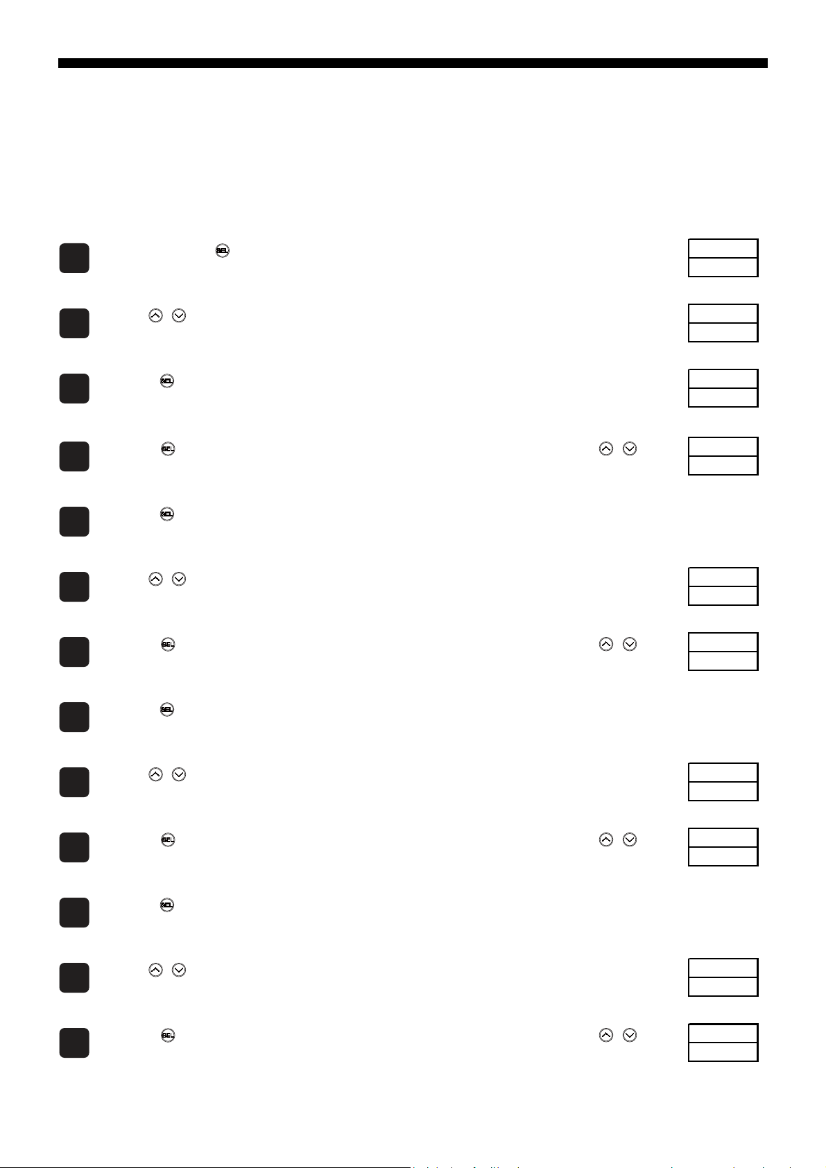
4. Setting Communication Parameters
List of Setting Parameters ...................................................16
Parameter Setting Procedure..............................................17
5. MODBUS Communication Protocol
Overview..............................................................................20
Message Composition.........................................................21
Calculating Error Check Code (CRC-16).............................24
Transmission Control Steps.................................................25
Prercautions when Writing Data..........................................26
7. Address Map and Data Format
Data Format.........................................................................38
Internal Calculation Value Data Address Map.....................40
8. Sample Program
Sample Program..................................................................68
9. Cooperative operation
Overview..............................................................................70
Connection...........................................................................71
Setup and related parameters .............................................72
Cooperative operation..........................................................73
List of parameters subject to the cooperative operation......74
10. Programless communication
Overview..............................................................................82
Connection...........................................................................83
Programless communication................................................84
Setup and related parameters .............................................88
Setup for Programless Communication ...............................90
11. Troubleshooting
Troubleshooting..................................................................126
6.
Command and Transmission Frame Details
Reading Data ......................................................................28
Writing Data.........................................................................32
– 2 –
Page 4

Chapter 1
Communication Functions
Overview – 4
– 3 –
Page 5
Overview
Caution
• The micro controller is equipped with communication functions fr om the RS-485 interface and PC loader interface, which
enables the transmission and reception of data between such devices as the personal computer, programmable controller,
and graphic panel.
• The version with RS-485 communication can provide the following three function s.
1. MODBUS RTU communication Typical master/stave communication is available. A PC or PLC acts as a master, while multiple
temperature controllers act as slaves. Communication is made in such a way that the master
sends messages to the slaves, and the slaves respond to it.
2. Cooperative operation When you control one temperature controller, the other controllers follow it. The one controller
3. Programless communication Programmable controller (PLC) can read the data of temperature controllers or write data on
The following is the description for MODBUS RTU communication. For cooperative operation and programless
communication, refer to Chapter 9 "Cooperative operation" and/or Chapter 10 "Programless communication".
• The communication system is composed of a master and slave relationship. Up to thirty-one slaves (micro controllers) may
be connected to one master (such as a personal computer) based on a “single master/multiple slave” method.
• However, the master can only communicate with one slave at a time. Therefore, each slave is specified by the "Station No."
setting.With PC loader communication, only one slave can be connected to one master.
Caution
• Systems constructed with the micro controller as slaves do not respond to messages issued by the master
with broadcast queries where the station number is "0".
• PC loader communication is not compatible with the multiple slave method.
acts as a master, while other controllers act as slaves. When you change the settings of the
master controller, a message will be sent to all slave controllers which follow the change.
temperature controllers without preparing a rudder program. One PLC acts as a master, and
multiple temperature controllers act as slaves. Each temperature controller in turn carries out
master-slave communication with PLC. The communication protocol is MODBUS RTU.
• In order to have proper communication between master and slave, the transmission data must be in the same format. This
document explains how to transmit data using the MODBUS protocol format.
• When using equipment with an RS-232C interface, such as a personal computer, as the master, make sure to use an RS-
232C to RS-485 converter.
• When using PC loader communication, you can use communication with the personal computer by connecting the PC loader
interface on the bottom of this unit with the PC loader communication cable (model: ZZP
TQ501923C3) sold separately.
*
RS-232C to RS-485 converter (recommended product)
Model Manufacturer URL Baud rate
KS3C-10 (isolated type) OMRON Corporation http://www.omron.co.jp Maximum 38400 bps
SI-30FA (isolated type) LINEEYE Co., Ltd. http://www.lineeye.co.jp Maximum 115.2 Kbps
– 4 –
Page 6
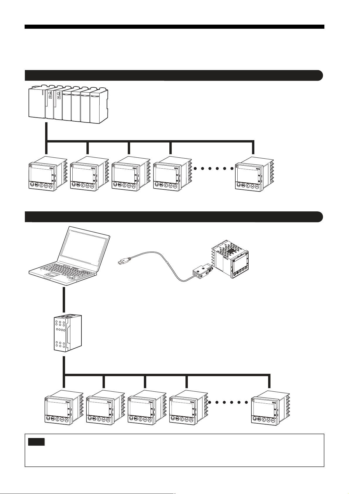
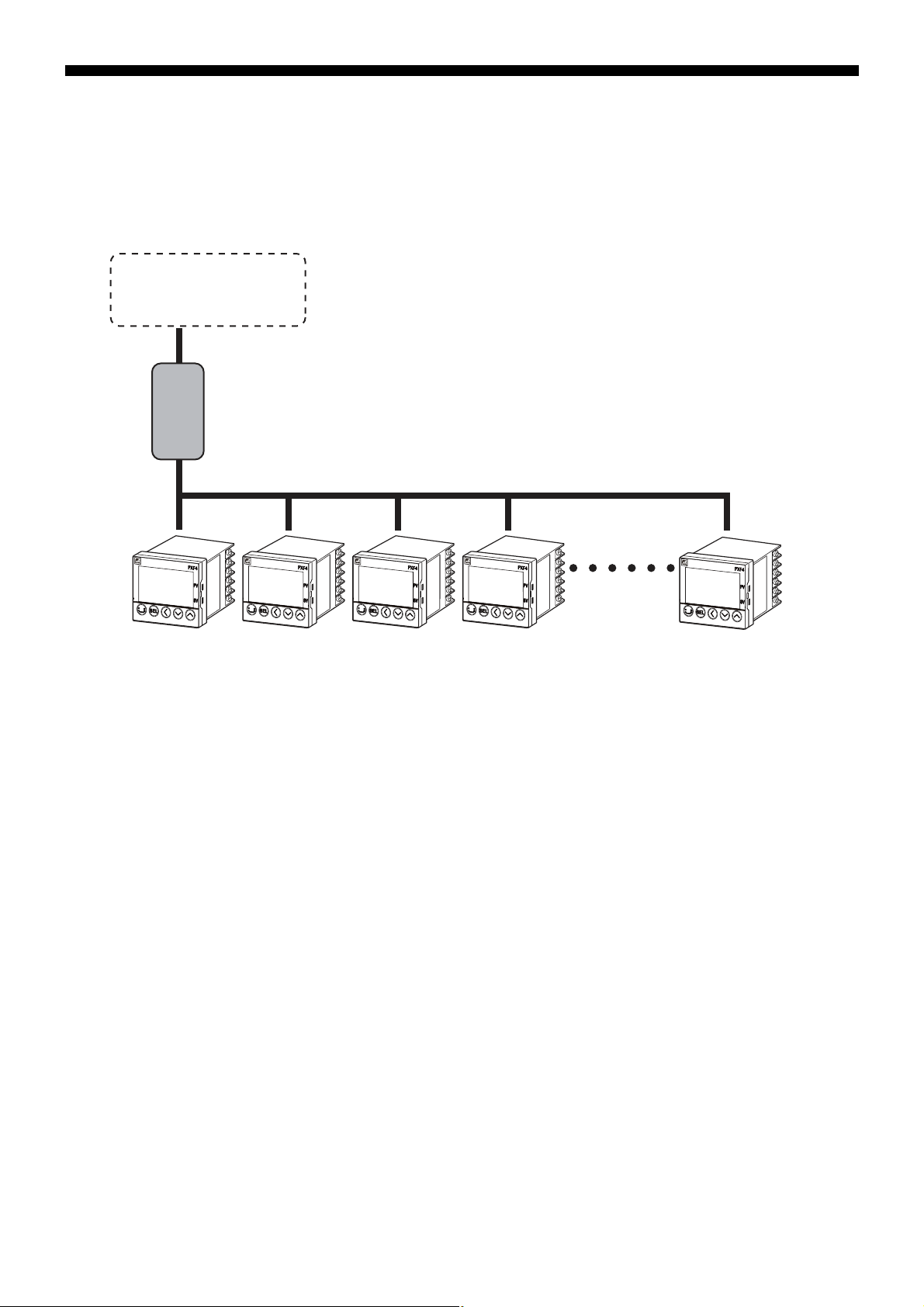
Connecting to a programmable controller
Caution
Programmable
controller
RS-485
PXF Series
Connecting to a personal computer
Personal
computer
PC loader communication cable
RS-232C
RS-232C to RS-485 converter
RS-485
PXF Series
When using the RS-232C to RS-485 converter, check to make sure that the cable is properly connected between the
converter and master. Communication will not work properly if the connection is incorrect.
Also be sure to correctly set the communication settings (such as communication speed and parity) on the RS-2 32C
to RS-485 converter. Communication will not work properly if the settings are incorrect.
– 5 –
Page 7

MEMO
– 6 –
Page 8

Chapter 2
Specifications
Communication Specifications – 8
– 7 –
Page 9
Communication Specifications
RS-485
Item Specifications
Electrical specifications EIA RS-485 compliant
Communication method Two wire system, half double-bit serial
Synchronous method Asynchronous
Connection status 1:N
Max. no. of connections 31 units
Communication distance Max 500m (total length)
Communication speed 9600bps, 19200 bps, 38.4kbps, 115.2kbps
Data format Data length 8 bits
Stop bit 1 bit
Parity None/Even/Odd (Selectable)
Transmission code HEX value (MODBUS RTU mode)
Error detection CRC-16
Insulation Functional insulation for the transmission area and
other areas (withstanding AC 500V)
PC Loader Interface
Item Specifications
Electrical specifications TTL Level
Communication method 3wire system, half double-bit serial
Synchronous method Asynchronous
Connection status 1:1
Station No. 1 (Not to be changed)
Communication speed 38.4kbps (Not to be changed)
Data format Data length 8 bits
Stop bit 1 bit
Parity none (Not to be changed)
Transmission code HEX value (MODBUS RTU mode)
Error detection CRC-16
Insulation Non-insulated internal circuit
– 8 –
Page 10

Chapter 3
Connection
Communication Terminal Configuration – 10
●
Wiring – 11
– 9 –
Page 11
Warning
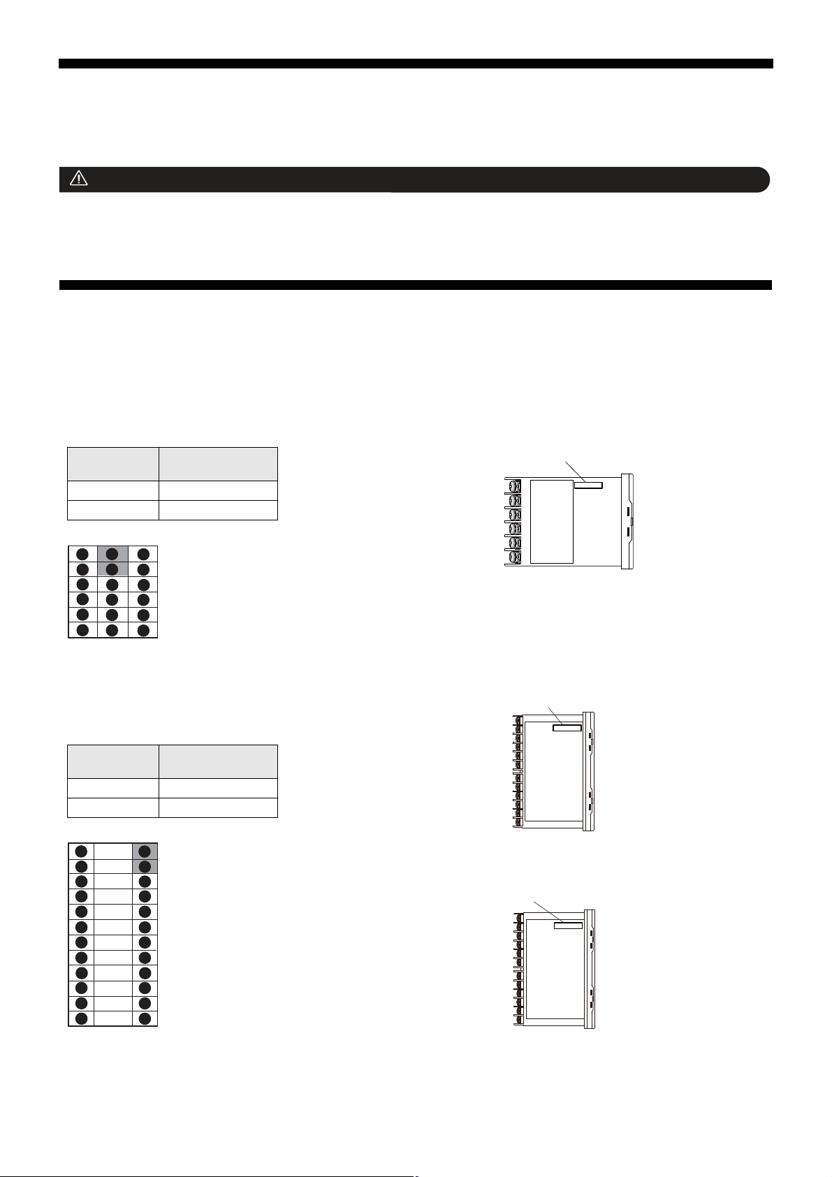
■ RS-485 (rear terminal)
PXF4
PXF5, PXF9
Terminal
Number
Signal Name
7 RS-485 +
8 RS-485 -
Terminal
Number
Signal Name
25 RS-485 +
26 RS-485 -
1
2
3
4
5
6
7
8
9
10
11
12
13
14
15
16
17
18
1
2
3
4
5
6
7
8
9
10
11
12
25
26
27
28
29
30
31
32
33
34
35
36
■ PC Loader Interface
PXF4
PXF5
PXF9
Do not turn on power until all of the wiring is completely finished.
There is a risk of electrical shock or damage.
Communication Terminal Configuration
PC Loader Interface
PC Loader Interface
PC Loader Interface
– 10 –
Page 12
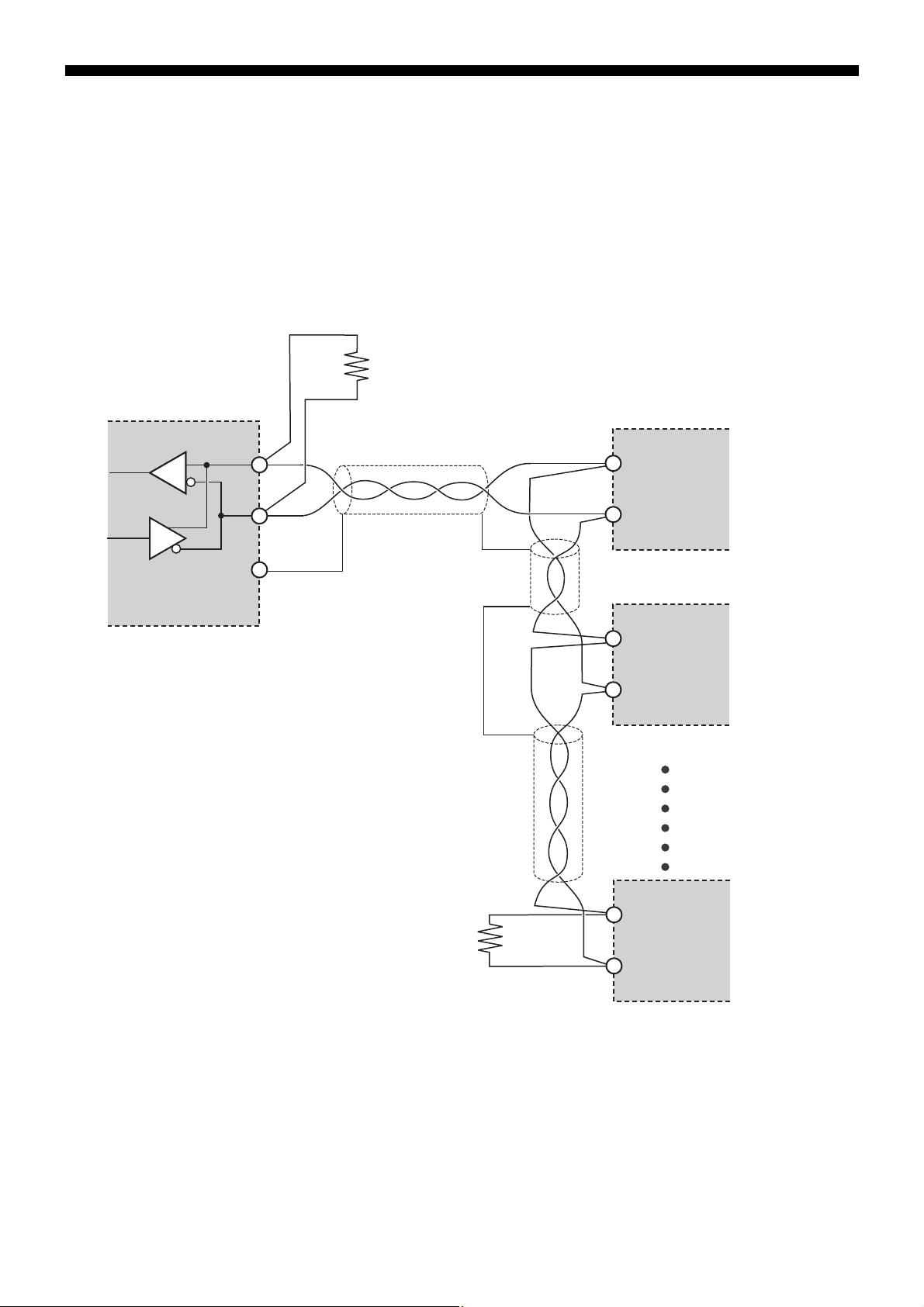
Wiring
Master
SG
Slave
+
–
+
–
Shielded twist pair cable
Terminating resistance
100W (1/2W)
Terminating resistance
100W (1/2W)
PXF Series
PXF Series
PXF Series
RS-485 interface
or
RS-485 side of
RS-232C to RS-485 converter
+
–
+
–
■ RS-485
• Please use a shielded twist pair cable. (Recommended cable: KPEV-SB (made by The Furukawa Electric Co., Ltd.))
• The maximum cable length should be 500m. One master and up to thirty-one micro controllers (slaves) can be connected per
circuit.
• Terminate both ends of the circuit with a terminating resistance of 100Ω (1/2W or more).
• Ground the shielded cable once towards the master side.
• SG does not have to be connected, but it can be used as an effective countermeasure against communication errors due to
noise.
– 11 –
Page 13
• When using the micro controller in an area where the imp ose d noise level is expected to exceed 1000V, we recommend using
Noise filter
Programmable controller
or
Personal computer
+ RS-232C to RS-485 converter
RS-485
PXF Series
a noise filter on the master side as seen in the figure b el ow.
[Noise filter] (recommended): ZRAC220 3-1 1 (ma de by TDK Corporation)
• If there are problems with EMC during communication, the noise l evel can be reduced by using a communication cable with a
ferrite core.
Ferrite core (recommended): ZCAT series (made by TDK Corporation)
MSFC series (made by Morimiya Electric Co., Ltd.)
– 12 –
Page 14
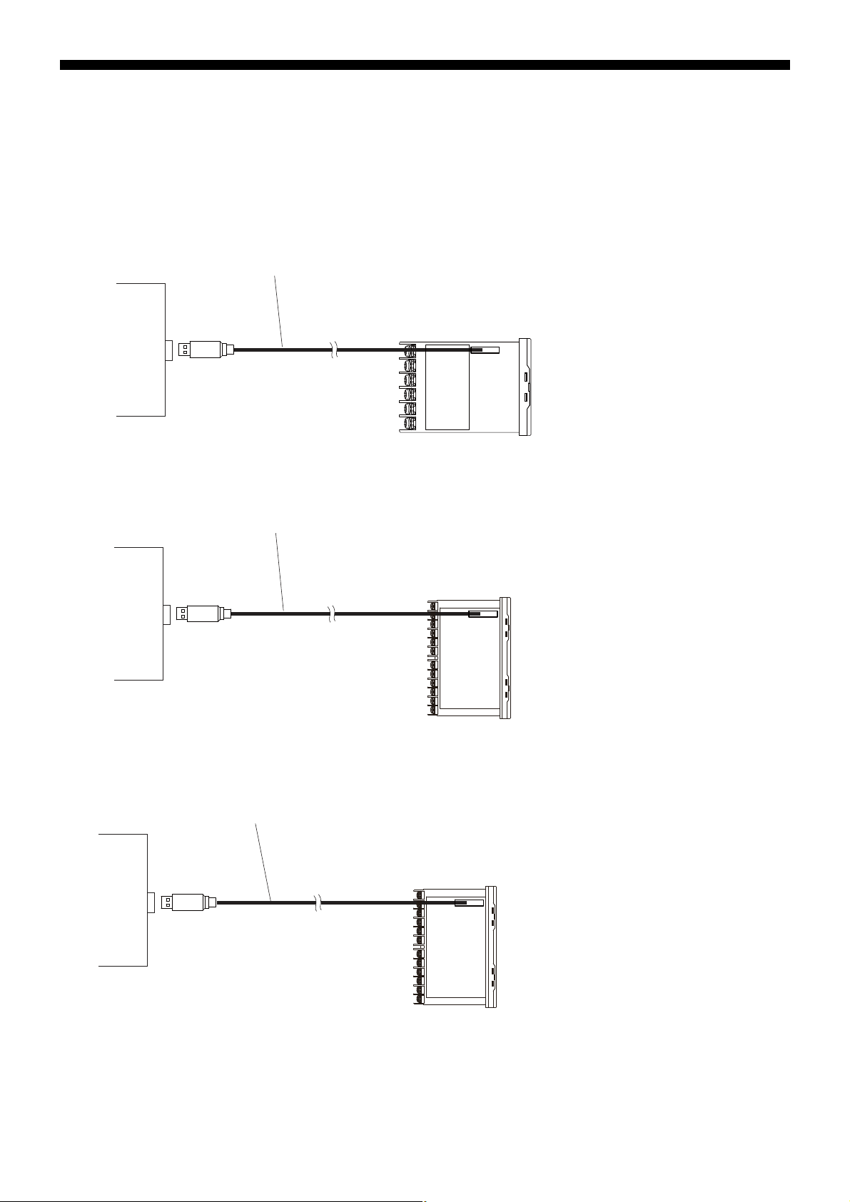
■ PC Loader Interface
PC loader communication cable
Master side
USB
PXF4 Left view
Personal
computer
etc.
ZZP
*
TQ501923C3
Master side
PXF5 Left view
Personal
computer
etc.
PC loader communication cable
ZZP
*
TQ501923C3
USB
• Use the PC loader communication cable sold separately.
PXF4
PXF5
PXF9
Master side
Personal
computer
etc.
USB
PC loader communication cable
TQ501923C3
ZZP
*
PXF9 Left view
– 13 –
Page 15

MEMO
– 14 –
Page 16

Chapter 4
Setting Communication Parameters
List of Setting Parameters – 16
●
Parameter Setting Procedure – 17
– 15 –
Page 17

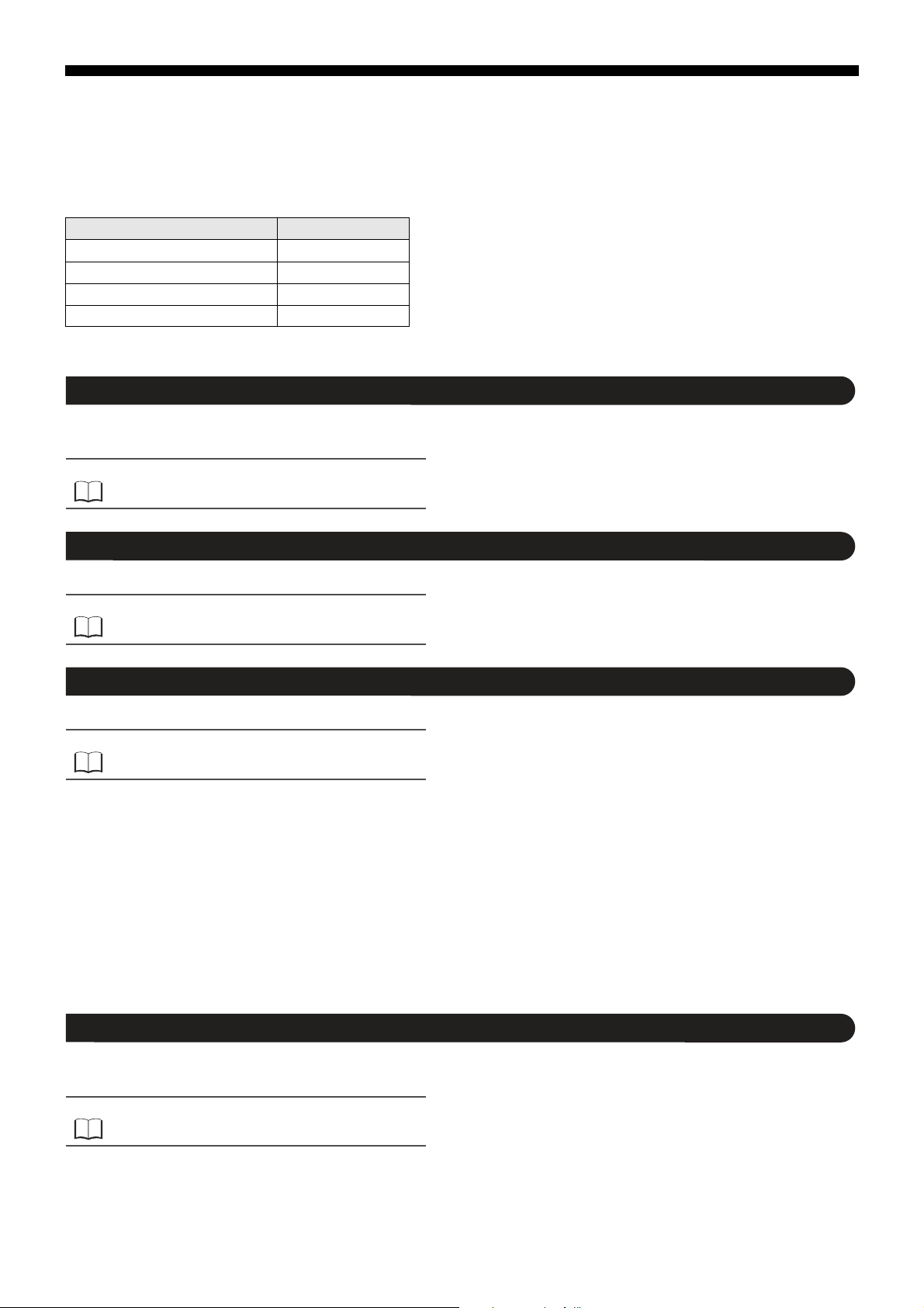
The following settings are required for proper communication between the master and micro controller units.
• The communication parameters for the master and all of the units must be set the same.
• During RS-485 communication, all of the micro controllers on a circuit must b e set with different "Station No. (STno)" other
than "0 (zero)". (Multiple micro controllers must not have the same "Station No.".)
• When using the PC loader interface, settings are not necessary on the main unit (the micro controller).
List of Setting Parameters
The setting parameters are shown in the chart shown below. Change the settings using the keys on the front of the micro
controller.
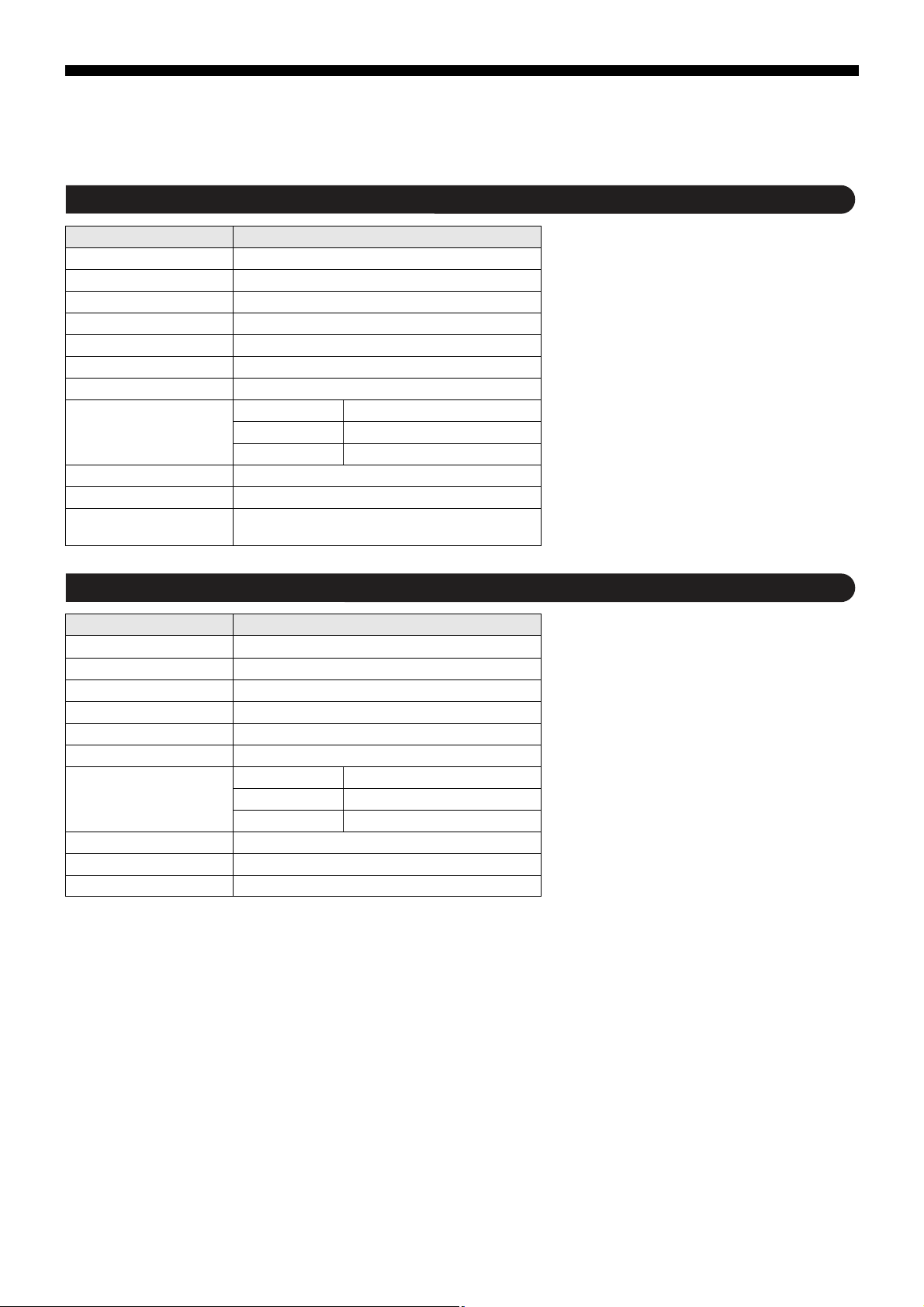
■ RS-485 (controller side)
Parameter
channel
CoM CH9
Screen
Parameter
No.
760
761
762
763
764
767
display
symbol
CTYP Communication
StNo Station No. 0 to 255 (0: unresponsive
SPEd RS-485 baud rate 96: 9600 bps
PRty RS-485 parity none
iNtV RS-485 response
SCC Communication
–
–
– Data length Fixed (cannot be changed) 8 bits Set the master and all of the slaves with
– Stop bit Fixed (cannot be changed) 1 bits Set the master and all of the slaves with
Name Setting range
0: MODBUS RTU
type
interval
permissions
1: Cooperative operation
2: Programless communication
communication)
192: 19200 bps
384: 38400 bps
115K: 115 Kbps
odd
even
0 to 100 1 Widen the time interval of receiving
r: read only
rW: read/writable
Initial
value
0 Select "0: MODBUS RTU".
1 Sets the station number.
96 Sets the baud rate
odd Sets the parity check
response. (Set value x 20 ms)
rW Sets whether or not overwriting is
possible from the master side (PC, etc.)
the same settings.
the same settings.
Remarks
■ Loader interface (main unit side)
The parameters do not need to be set. Set the loader software (master) with the following settings.
• Communication speed: 38400 bps
• Parity: none
– 16 –
Page 18
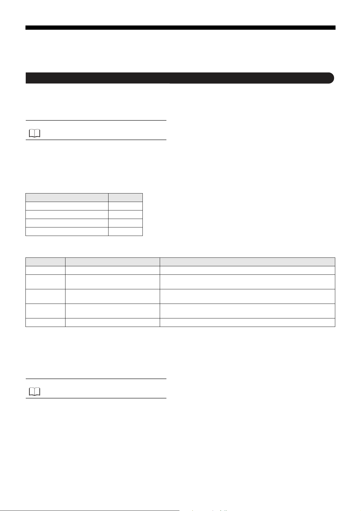
Parameter Setting Procedure
Pid
1
CoM
2
0
3
"3"
4
5
96
6
"96"
7
8
odd
9
"NoNE"
10
11
R
12
"WR"
13
The following steps explain how to change the settings to station number "3", parity setting "9600bps/none", and communication
permissions "read and writable" as an example.
Press and hold the key to move to "channel selection mode".
Use the keys to select "CoM CH9".
Press the key to display "StNo".
Press the key, and whe n the bottom part of the display begins to blink, use the
keys to select "3".
The station number "3" is selected.
Press the key to set.
Use the keys to select "SPEd".
Press the key, and whe n the bottom part of the display begins to blink, use the
keys to select "96".
The RS-485 baud rate is set to "9600 bps".
CH 1
CH 9
StNo
StNo
SPEd
SPEd
Press the key to set.
Use the keys to select "PRty".
Press the key, and whe n the bottom part of the display begins to blink, use the
keys to select "NoNE".
The RS-485 parity is set to "none".
Press the key to set.
Use the keys keys to select SCC ("SCC").
Press the key, and whe n the bottom part of the display begins to blink, use the
keys to select "WR".
Communication permissions is set to "read/writable".
PRty
PRty
SCC
SCC
– 17 –
Page 19

Press the key to set.
14
15
16
Press the key to return to the operation mode PV/SV screen.
Turn the power to the micro controller off and on a g ain.
The changes to the communication parameters become effective after the power turns off and on
again.
– 18 –
Page 20

Chapter 5
MODBUS Communication Protocol
Overview – 20
●
Message Composition – 21
●
Calculating Error Check Code (CRC-16) – 24
●
Transmission Control Steps – 25
●
Prercautions when Writing Data – 26
– 19 –
Page 21

Overview
Master Slave
Command Message
Response Message
Station number is the same
The communication system with the MODBUS protocol always operates using a method where the master first sends a command
message and the applicable slav e re plys with a respo nse message .
The following describes the communication steps.
Master sends the command
message for the slave.
The slave checks whether the station
number in the received message is
the same as its own station number.
When it’s the same When it’s not the same
The slave runs the command and
sends a response message.
The slave throws out the received
message and waits for the next
command message. (No reply.)
● When the station number in the command message is the same as the unit’s station number
● When the station number in the command message is not the same as the unit’s station number
Master Slave
The master can communicate with an individual slave when multiple slaves are connected on the same circuit by the station
number specified in the master’s command message.
Command Message
Station number is not the same
– 20 –
Page 22
Message Composition
Refer to
Refer to
Refer to
Refer to
The command message and response message are composed of four parts: the station number, function code, data part, and
error check code. These four parts are sent in that order.
Field name No. of bytes
Station No. 1 byte
Function Code 1 byte
Data Part 2 to 125 bytes
Error Check Code (CRC-16) 2 bytes
The following describes each part of the message.
Station No.
This is the number specifying the slave. Commands can only be processed by slaves that have the same value set in the "STno"
parameter.
For more about setting the "STno" parameter, see "Chapter 4,
Setting Communication Parameters" (p. 15).
Function Code
This code specifies the function for the slave to perform.
For more about function codes, see "Function Code" (p. 23).
Data Part
This data is required to run the function code. The composition of the data part is different depending on the function code.
See "Chapter 6, Command and Transmission Frame Details"
(p. 27).
The data in the micro controller is assigned a coil number or resistor number. This coil number or resistor number is specified
when the data is read or written through communication.
The coil number or resistor number used by the message employs a relative address.
The relative address is calculated using the following formula.
Relative address = (last four digits of the coil number or resistor number) – 1
(Ex.) When a function code specifies resistor number "40003"
Relative address = (the last four digits of 40003) – 1
= 0002
is used in the message.
Error Check Code
This code detects whether there are errors (changes in the bits) dur ing the signal transmission processes. MODBUS protocol
(RTU mode) uses CRC-16 (Cyclic Redundancy Check).
For more about calculating CRC, see Section 5,
"Calculating Error Check Code (CRC-16)" (p. 24).
– 21 –
Page 23
Slave Response
Refer to
Refer to
■ Normal Slave Response
The slave creates and replies with a response message for each command message. The response message has the same
format as the command message.
The contents of the data part are different depending on the function code.
See "Chapter 6, Command and Transmission Frame Details".
■ Irregular Slave Response
If there are problems (such as specification of a nonexistent function code) with the contents of the command message other than
transmission error, the slave creates and replies with an error response message without following the command.
The composition of the error response message uses the value of the function code in the command message plus 80
below.
Field name No. of bytes
Station No. 1 byte
Function Code +80
H 1 byte
Error Code 1 byte
Error Check Code (CRC-16) 2 bytes
The error code is shown as follows.
Error Code Contents Explanation
H Faulty function code A nonexistent function code was specified. Please check the function code.
01
H Faulty address for coil or resistor The specified relative address for the coil number or resistor number cannot be
02
used by the specified function code.
03
H Faulty coil or resistor number The specified number is too large and specifies a range that does not contain
04
H Write inhibited Data writing via communication is prohibited. “SCC” parameter is set to “R: read
06
H Busy EEPROM is busy in writing. Wait for a few seconds, and then retry writing.
coil numbers or resistor numbers.
only”.
H, as seen
■ No Response
In the following situations, the slave will ignore the command message and not send a response message.
• The station number specified by the command message is not the same as the slave’s specified station number.
• The error check code does not correspond, or a transmission error (such as parity error) is detected.
• The interval between the data comprising the message is empty for more than 24 bit time.
See Section 5 "Transmission Control Steps" (p. 25).
• The slave station number is set to "0".
– 22 –
Page 24
Function Code
For MODBUS protocol, coil numbers or resistor numbers are assigned by the function code, and each function code
only works for the assigned coil number or resistor number.
The correspondence between the function code and the coil number or resistor number is as follows.
Function Code Coil Number, Resistor Number
Code Function Target Number Contents
H Read (continuous) Hold resistor 3xxxx Read word data
03
04
H Read (continuous) Input resistor
H Write Hold resistor
06
H Write (continuous) Retention resistor
10
The message length for each function is as follows.
Code Contents
H Read word data 60 words
03
H Read word data (read-only) 60 words
04
06
H Write word data 1 word 8888
H Continuously write word data 60 words
10
Assignable
Data Number
*1
*1
*1
Command Message Response Message
Minimum Maximum Minimum Maximum
4xxxx
Read/write word data
[unit: byte]
887125
887125
11 129 8 8
*1: "Assignable Data Number" above is limited by the data number that the micro controller assigned to the coil number or
address number.
(Excluding function code 06
H).
– 23 –
Page 25
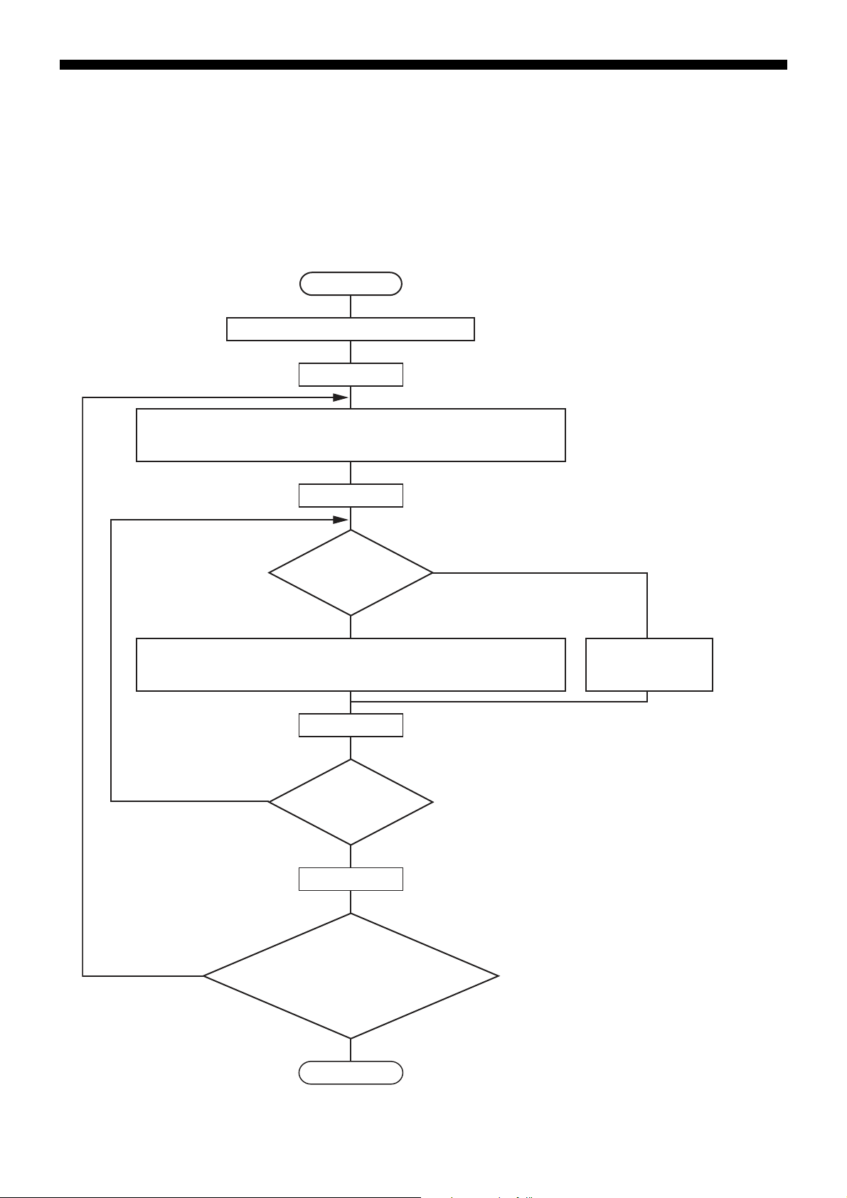
Calculating Error Check Code (CRC-16)
YES
YES
NO
NO
YES
* Description of Variables
CR : CRC error check data (2 byte)
J : Command message calculation
character digit
K : No. of times to check CR calculation
Start
Set J = 1
Set K = 1
Add 1 to K
Complete
Add 1 to J
Set CR to FFFF
H (hexadecimal)
Exclusive-or (XOR) runs on each character of J (one byte) for CR
and the specified message, and sets that result to CR.
After CR has been adjusted one bit to the right, A001
H and XOR
run and set that result to CR.
Is the right-hand
bit for CR 1?
NO
Adjust CR one bit
to the right.
Has calculation
finished 8 times ?
J > 8
Has every character
been calculated ?
J > Number of characters
(Calculations occur in the order
command message station number,
function code, and data.)
The CR calculation result is added
onto the end of the command
message in LOW or HIGH order.
CRC-16 is a 2-byte (16-bit) error check code. The calculation range extends from the start of the message (station number) to the
end of the data part.
The slave calculates the CRC of the received message and ignores the message if this value is not the same as the received
CRC code.
CRC-16 is calculated as follows.
– 24 –
Page 26

Transmission Control Steps
Caution
Master Communication Method
Start communication from the master while following the rules below.
1. The command message, must be sent after an empty space of at least 48 bit time.
2. The interval between each byte in a command message should be less than 24 bit time.
3. After sending a command message, for less than 24 bit time the master will enter receiving standby.
4. After receiving the response message, the next command message must be sent after at least 48 bit time. (Similar to #1.)
5. For safety reasons, create a framework where the master checks the response message, and if there is no response or an
error occurs, retry at least three times.
The definitions written above are for the minimum required value. For safety reasons, we recommend creating a
master side program that keeps margins two to three times as large. For a concrete example, with 9600 bps, we
recommend programming a blank state (#1 above) of at least 10ms, and the interval between bytes (#2 above) and
switching time from sending to receiving (#3 above) within 1 ms.
Explanation
■ Frame Detection
This communication system uses a two-wire RS-485 interface, and the circuit can therefore enter one of the following two states.
• Empty state (no data on the circuit)
• Communication state (data running on the circuit)
The units connected on the circuit start in receiving state and monitor the circuit. When a blank state appears on the circuit f or at least
24 bit time, the unit detects the end of the previous frame, and within the next 24 bit time, enters receiving standby. When data
appears on the circuit, the unit begins receiving data, and once another blank state of at least 24 bit time is detected, that frame is
ended. In other words, the data on the circuit from the first time that a 24 bit time blank state appears to the second time one appears
is loaded as one frame (a bundle of data). Therefore, one frame (command message) must be sent while following the rules below.
• Before sending the command message, leave an empty space of at least 48 bit time.
• The interval between each byte in a command message should be less than 24 bit time.
■ Micro controller Response
After the micro controller detects the frame (detects blank states at least 24 bit time long), that frame is used to send a command
message. When a command message is sent locally, the response message is returned, but the processing time is about 1 to 30
ms. (The time may change depending on the contents of the command message. ) Therefore, one frame (command message)
must be sent while following the rules below.
– 25 –
Page 27
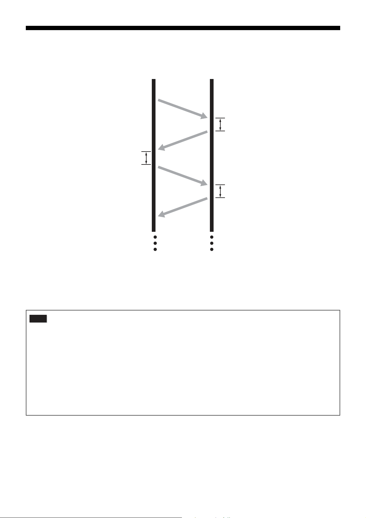
• After sending a command message, for less than 24 seconds the master will enter receiving standby.
Caution
Master
POL1
POL1 response data
POL2 response data
Slave
POL2
1 to 30ms
1 to 30ms
Interval of at least 10ms required
(at least 20ms recommended)
Prercautions when Writing Data
PXF contains internal nonvolatile memory (EEPROM) that is used to save the setting parameters. The data written to the
nonvolatile memory (EEPROM) remains even after the power for PXF is turned off. Parameters that are written via
communication are automatically saved in the internal nonvolatile memory (EEPROM). However, please note that there are two
limitations as follows.
1. There is a limit to the number of times that data can be transferred to the nonvolatile memory (EEPROM)
(100,000 times). Data cannot be guaranteed if written more than 100,000 times.
Be careful not to transfer unnecessary data when writing data via communication.
In particular, when constructing a communication system with master POD (such as a touch panel), make sure
that the POD writing and trigger settings are appropriate.
Avoid writing at fixed cycles.
2. Writing to the nonvolatile memory (EEPROM) takes seve ral milliseconds . If the pow er f or PXF is turned off during
this operation, the data saved to the nonvolatile memory (EEPROM) may be corrupted.
Wait several seconds after writing data before turning off the power.
In particular, when writing data in a cycle from master device, there is a greater danger of the writing timing and
power shutoff timing coinciding.
Avoid writing at fixed cycles.
– 26 –
Page 28

Chapter 6
Command and Transmission Frame
Details
Reading Data – 28
●
Writing Data – 32
– 27 –
Page 29
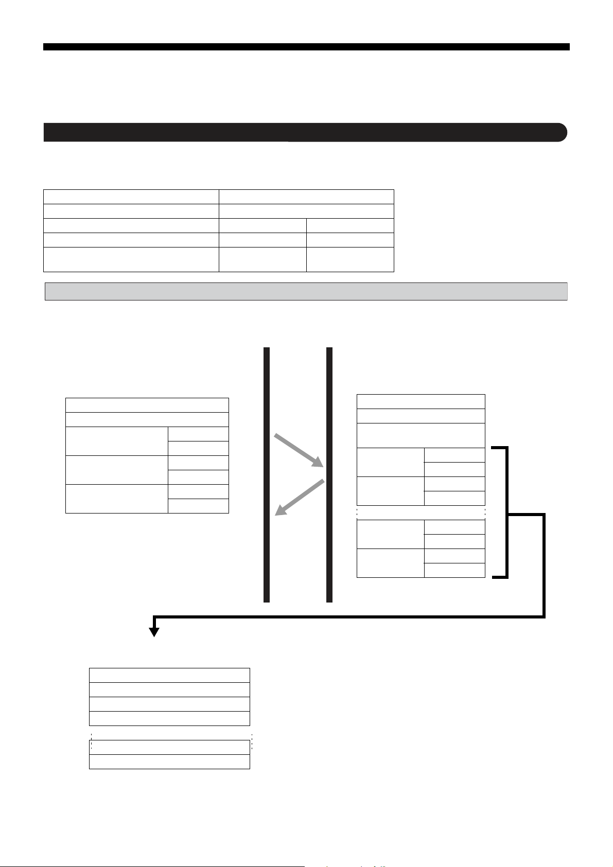
Reading Data
Master Slave
Command Message Composition
(bytes)
Station No.
Function Code
No. to Start Reading
(Relative Address)
Upper
Lower
No. of Words to Read
(1 to 60 words)
Upper
Lower
CRC Data
Upper
Lower
Reply Message Composition (bytes)
Station No.
Function Code
No. of Bytes to Read
(No. of Words to Read x 2)
First Word Data
Contents
Upper
Lower
Next W ord Da ta
Contents
Upper
Lower
Last Word D a t a
Contents
Upper
Lower
CRC Data
Upper
Lower
■ Meaning of Read Word Data
MSB LSB
First Word Data upper byte
First Word Data lower byte
Next Word Data upper byte
Next Word Data lower byte
Last Word Data upper byte
Last Word Data lower byte
Reading Word Data (Function Code: 03H)
The unit reads word data continuously for the specified number of words from the first number to start reading from.
The slave forwards the read word data from the upper number of bytes to the lower number.
Function Code 03H
Max. No. of Words to Read in One Message 60 words
Relative Address 0000H to 07CFH
Resistor Number 40001 to 42000 42001 to 45032
Contents
Internal Calculation
Value
Message Composition
H to 013AH
07D0
Engineering Unit
– 28 –
Page 30
Example of Transmitting a Message (For Engineering Unit)
Refer to
Master Slave
Command Message (bytes)
Station No. 02H
Function Code 03H
No. to Start Reading
(Relative Address)
Upper 07H
Lower E7H
No. of Words to Read
Upper 00H
Lower 02H
CRC Data
Upper 78H
Lower 95H
Response Message (bytes)
Station No. 02H
Function Code 03H
No. of Bytes to Read 04H
First Word Data
Contents
Upper 00H
Lower 00H
Next Word
Data Contents
Upper 01H
Lower 90H
CRC Data
Upper C8H
Lower CFH
The message is composed as fo ll ows when reading the PV input lower limit and PV input upper limit from station number 2.
• PV Lower Limit Relative Address: 07E1H
■ Meaning of Read Data
PV Input Lower Limit 00 00H = 0
PV Input Upper Limit 01 90H = 400
If Decimal Point Position = 0, then the PV input upper limit and lower limit are as follows.
PV Lower Limit = 0°C
PV Upper Limit = 400°C
For more about the internal calculation value, engineering unit,
and decimal point see
"Chapter 7, Address Map and Data Format" (p. 39).
– 29 –
Page 31

Reading Read-Only Word Data (Function Code: 04H)
Master Slave
Command Message Composition
(bytes)
Station No.
Function Code
No. to Start Reading
(Relative Address)
Upper
Lower
No. of Words to Read
(1 to 60 words)
Upper
Lower
CRC Data
Upper
Lower
Reply Message Composition (bytes)
Station No.
Function Code
No. of Bytes to Read
(No. of Words to Read x 2)
First Word Data
Contents
Upper
Lower
Next W ord Data
Contents
Upper
Lower
Last Word Data
Contents
Upper
Lower
CRC Data
Upper
Lower
■ Meaning of Read Word Data
MSB LSB
First Word Data upper byte
First Word Data lower byte
Next Word Data upper byte
Next Word Data lower byte
Last Word Data upper byte
Last Word Data lower byte
The unit reads word data continuously for the specified number of words from the first number to start reading from.
The slave forwards the read word data from the upper number of bytes to the lower number.
Function Code 04H
Max. No. of Words to Read in One Message 60 words
Relative Address 0000H to 07CFH
Resistor Number 30001 to 32000 32001 to 32240
Contents Internal Calculation Value Engineering Unit
Message Composition
H to 08BFH
07D0
– 30 –
Page 32

Example of Transmitting a Message (Internal Calculation Data)
Refer to
Refer to
Master Slave
Command Message (bytes)
Station No. 01H
Function Code 04H
No. to Start Reading
(Relative Address)
Upper 00H
Lower 00H
No. of Bits to Read
Upper 00H
Lower 01H
CRC Data
Upper 31H
Lower CAH
Response Message (bytes)
Station No. 01H
Function Code 04H
No. of Bytes to Read 02H
First Word Data
Contents
Upper 03H
Lower 46H
CRC Data
Upper 38H
Lower 32H
Master Slave
Command Message (bytes)
Station No. 01H
Function Code 04H
No. to Start Reading
(Relative Address)
Upper 07H
Lower D0H
No. of Words to Read
Upper 00H
Lower 01H
CRC Data
Upper 47H
Lower 31H
Response Message (bytes)
Station No. 01H
Function Code 04H
No. of Bytes to Read 02H
First Word Data
Contents
Upper 01H
Lower 4FH
CRC Data
Upper F9H
Lower 54H
The message is composed as follows when reading the PV input value from station number 1.
• PV value relative address: 0000H Number of data: 01H
■ Meaning of Read Data
Word Data Contents 03 46H = 838 (8.38% FS)
When the input range is 0 to 400°C
PV = 33.5°C (= 8.38% FS x 400 (input range width)
For more about the internal calculation value, engineering unit,
and decimal point see
"Chapter 7, Address Map and Data Format" (p. 39).
Example of Transmitting a Message (For Engineering Unit)
The message is composed as follows when reading the PV value from station number 1.
• PV value relative address: 07D0H Number of data: 01H
■ Meaning of Read Data
Word Data Contents 01 4FH = 335
When the decimal point position = 1
PV = 33.5°C
For more about the internal calculation value, engineering unit,
and decimal point see
"Chapter 7, Address Map and Data Format" (p. 39).
– 31 –
Page 33

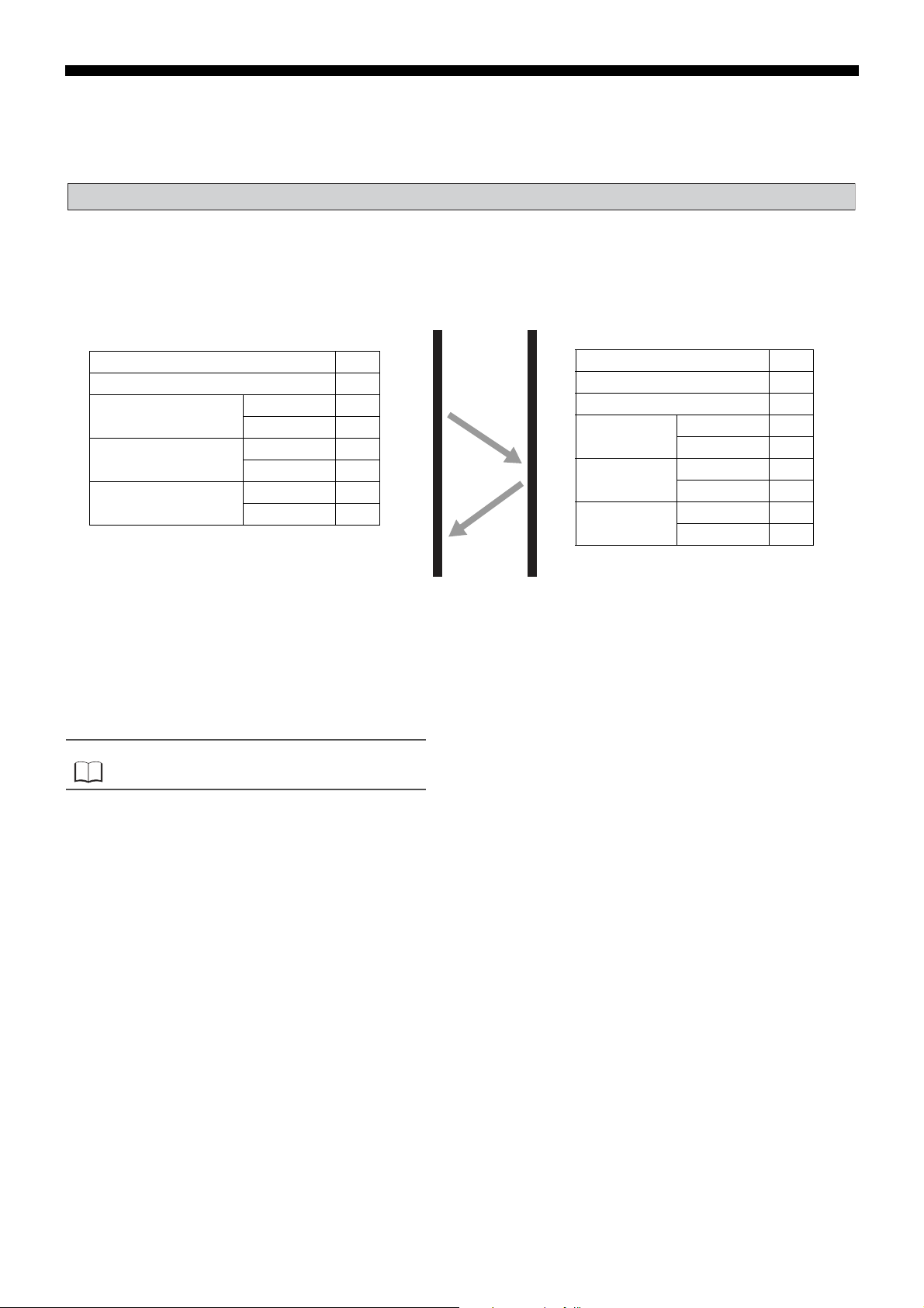
Writing Data
Master Slave
Command Message Composition
(bytes)
Station No.
Function Code
Specified Write Number
(Relative Address)
Upper
Lower
Word Data to Write
Upper
Lower
CRC Data
Upper
Lower
Response Message Composition
(bytes)
Station No.
Function Code
Specified Write
Number
(Relative Address)
Upper
Lower
Word Data to
Write
Upper
Lower
CRC Data
Upper
Lower
Writing Word Data (1 word, function code: 06H)
This writes the specified data to the specified number for word data. The master sends the data to be written from the upper
number of bytes to the lower number.
Function Code 06H
Max. No. of Bits to Read in One Message 1 words
Relative Address 0001H to 07CFH 07D0H to 13A7H
Resistor Number 40004 to 42000 42001 to 45032
Contents Internal Calculation
Value
Message Composition
Engineering Unit
– 32 –
Page 34

Example of Transmitting a Message
Point
Master Slave
Command Message (bytes)
Station No. 01H
Function Code 06H
Specified Write
Number
(Relative Address)
Upper 00H
Lower 05H
Word Data to Write
Upper 03H
Lower E8H
CRC Data
Upper 99H
Lower 75H
Response Message (bytes)
Station No. 01H
Function Code 06H
Specified Write
Number
(Relative Address)
Upper 00H
Lower 05H
Write Specification
State
Upper 03H
Lower E8H
CRC Data
Upper 99H
Lower 75H
This example explains how to set PID parameter "P" to 100.0 (1000D = 03E8H) on station number 1.
Parameter "P" relative address: 0005H (internal calculation value table)
07D5H (initial value table)
For more about the internal calculation value, engineering unit, and decimal point see "Sent Data Format" (p. 40).
– 33 –
Page 35

Writing Continuous Word Data (Function code: 10H)
Master Slave
Command Message Composition (bytes)
Station No.
Function Code
Specified Write
Number (Relative
Address)
Upper
Lower
No. of Words to Write Upper
Lower
No. of Bytes to Write
First Word Data to
Write
Upper
Lower
Next Word Data to
Write
Upper
Lower
Last Word Data to
Write
Upper
Lower
CRC Data Upper
Lower
Reply Message Composition (bytes)
Station No.
Function Code
Specified Write
Number (Relative
Address)
Upper
Lower
No. of Words to
Write
Upper
Lower
CRC Data Upper
Lower
■ Meaning of Read Word Data
MSB LSB
First Word Data upper byte
First Word Data lower byte
Next Word Data upper byte
Next Word Data lower byte
Last Word Data upper byte
Last Word Data lower byte
}
1 to 60
} No. of Words
to Write x 2
This writes continuous word information for a number of written words from the first number for writing.
The master sends the data to be written from the upper number of bytes to the lower number.
Function Code 10H
Max. No. of Bits to Read in One Message 60 words
Relative Address 0000H to 07CFH
Resistor Number 40001 to 42000 42001 to 45032
Contents Internal Calculation
Message Composition
Value
H to 13A7H
07D0
Engineering Unit
– 34 –
Page 36

Example of Transmitting a Message (Internal Calculation Data)
Point
Refer to
Master Slave
Command Message (bytes)
Station No. 01H
Function Code 10H
Specified Write
Number (Relative
Address)
Upper 00H
Lower 05H
No. of Words to
Write
Upper 00H
Lower 03H
No. of Bytes to Write 06H
First Word Data to
Write
Upper 03H
Lower E8H
Next Word Data to
Write
Upper 00H
Lower 64H
Last Word Data to
Write
Upper 00H
Lower 32H
CRC Data Upper 56H
Lower BEH
Response Message (bytes)
Station No. 01H
Function Code 10H
Specified Write
Number
(Relative Address)
Upper 00H
Lower 05H
Write Specification
State
Upper 00H
Lower 03H
CRC Data
Upper 90H
Lower 09H
The message is composed as follows when writing the following PID parameters to station number 1.
P = 100.0 (= 1000D = 03E8H)
I = 10 (= 100D = 0064)
D = 5.0 (= 50D = 0032H)
• Parameter “P” relative address: 0005H, Data number: 03H
The decimal point cannot be included in the sent data, so data such as “100.0” above is sent as “1000”.
For each type of send data format, see “Chapter 7, Address
Map and Data Format” (p. 39).
– 35 –
Page 37

MEMO
– 36 –
Page 38

Chapter 7
Address Map and Data Format
Data Format – 38
●
Internal Calculation Value Data Address Map – 40
– 37 –
Page 39

Data Format
Refer to
Caution
Sent Data Format
The MODBUS protocol used by this equipment employs RTU (Remote Terminal Unit) mode. The data is sent as "numerical
value", not as ASCII code.
Internal Calculation Value and Engineering Unit
In this unit, parameter data and data dependent on an input range can handle the following two types of data.
Internal Calculation Value: Values listed as percentages of the input range (0.00 to 100.00, without decimal point)
Engineering Unit: Values subjected to scaling to actual values depending on the input range
"Engineering Unit" data is handled as the address (resister num ber) of 2000 added to th e address (resiste r number) for "Internal
Calculation Value".
(Ex.) The value is calculated as follows when the full scale is 400°C and the PV value is "150".
Class Resistor Number Data (HEX) Data
Internal Calculation Value 30001 0EA6 (H)
Engineering unit 32001 0096 (H) 150
→
3750 (37.5%)
The PV value is received as follows.
37.50 (%) x 400 (full scale °C) = 150 °C
Data not dependent on an input range the same data in both addresses.
For more about data dependent on an input range, see
"Chapter 7 Address Map and Data Format" (page 39).
Pay attention to the position of the decimal point when changing the input range by writing with communication. When
changing the position of the decimal point by writing with communication, change the lower limit and upper limit of the
input range at the same time.
(Ex.) When changing the input range from 0 to 400 to 0.0 to 400.0
■ Operating the keys on the front of the equipment
Change the position of the decimal point ("Pvd") in the setup menu ("SET Ch 6").
"Pvd" = 0 → 1 (or 2)
■ Changing by communication
Set the decimal position parameter ("Pvd"), as well as the corresponding values for PF input lower limit ("Pvb") and PV input upper
limit ("PvF").
"Pvd" = 0 → 1
"Pvb" = 0 → 0
"PvF" = 400 → 4000
Managing the Decimal Point
Some of the internally stored data may contain may digits lower than the decimal point on the front display . Also , the decimal point
is not added to sent data.
Carry out processes for the decimal point position (erasing the d ecimal point when sending data and add ing the decimal point
when receiving data).
Attention must be paid to the position of the decimal point for data where the parameters are dependent on a range in "Chapter 7
Address Map and Data Format". Refer to Address Map.
– 38 –
Page 40

Data during Input Error
For situations such as overrange, underrange, and input breaks where "UUUU" or "LLLL" display on the front, read PV value
becomes 105% or -5% of the input range.
Input errors can be detected via communication using "resistor number 30008 (or 31008): Input/Unit Error Status".
Written Data
When writing data to each parameter, set that written data within the range for the data. PXF can accept wr itten data outside of
the range, but do so with care as correct operations are not guaranteed.
Addresses Not Written
Do not write to addresses that are not public. Doing so may cause damage.
– 39 –
Page 41

Internal Calculation Value Data Address Map
DisplayNo. Name Internal
Engineering
unit
Value
Function
Relative
address
Register No.
Read data Written data range
Factory-set
value
Dependent
on range
Remarks
1MAn Switchover between auto
and manual mode
Switches between auto and manual
modes
0084H40133 42133 0: oFF (auto)
1: on (manual)
oFF
2 STby Switchover between RU N
and standby
Switches the operation mode between
RUN and standby
0003
H
40004 42004 0: oFF (RUN)
1: on (standby)
oFF
4PrG
Ramp soak control command
Changes ramp soak run states 0051H40082 42082 0: oFF (stop)
1: rUn (during run)
2: hLd (during hold)
3: ENd (end)
4: GS
(during guarantee soak)
0: oFF (stop)
1: rUn (run)
2: hLd (hold)
oFF
5AT Auto-tuning run command Runs auto-tuning. 0004H40005 42005 0: oFF (stop/fini sh)
1: on (normal type)
2: Lo (low PV type)
oFF
6LACh Alarm output latch release
command
Cancels the alarm output latch state 00A0
H
40161 42161 0: oFF
1: rST (latch reset)
oFF
7 Svn SV selecti on Chooses the SV No. to be used for
control.
00DC
H
40221 42221 0: LoCL (local SV)
1: Sv1 (SV = SV1)
2: Sv2 (SV = SV2)
3: Sv3 (SV = SV3)
4: Sv4 (SV = SV4)
5: Sv5 (SV = SV5)
6: Sv6 (SV = SV6)
7: Sv7 (SV = SV7)
8: di (according to DI)
LoCL
8 PLn1 PID selection Chooses the PID No. to be used for
control.
00DDH40222 42222 0: LoCL (local PID group)
1: Pid1 (PID group No.1)
2: Pid2 (PID group No.2)
3: Pid3 (PID group No.3)
4: Pid4 (PID group No.4)
5: Pid5 (PID group No.5)
6: Pid6 (PID group No.6)
7: Pid7 (PID group No.7)
8: di (according to DI)
LoCL
9AL1 00A2
H
40163 42163
2.50%FS
10 AL1L ALM1 set value
11 AL1h 00A3
H
40164 42164
12 AL2 00A9
H
40170 42170
2.50%FS
13 AL2L
ALM2 set value
14 AL2h 00AA
H
40171 42171
15 AL3 00B0
H
40177 42177
2.50%FS
16
AL3L
ALM3 set value
17
AL3h 00B1H40178 42178
27 WCMd Electric power calculation
command
Switches the electric power calculation
status
031F
H
40800 42800
oFF
28 LoC Key lock Sets the key lock to prevent wrong
operation
0027
H
40040 42040 0: oFF (no lock)
1: ALL (all lock)
2: PArA (all but SV locked)
oFF
Sets the alarm value for ALM 3.Absolute value alarm: 0 to 100% FS
Deviati on alarm: -100 to 100% FS
0: oFF (off)
1: rUn (run)
2: hLd (hold)
Sets the alarm value for ALM 1. Absolute value alarm: 0 to 100% FS
Deviati on alarm: -100 to 100% FS
Sets the alarm value f
or ALM2. Absolute value alarm: 0 to 100% FS
Deviati on alarm: -100 to 100% FS
3 REM Local/remote switchover Switches SV between local/remote. 0074H40117 42117 LoCL (local)/
rEM (remote)
LoCL
When changing the
SV with the front key,
do not change the
“Svn” parameter via
communication.
Otherwise, the
changed SV may not
be stored correctly.
18 AL4 00B7H40184 42184
2.50%FS
19 AL4L
ALM4 set value
20 AL4h 00B8
H
40185 42185
21 AL5 00BE
H
40191 42191
2.50%FS
22 AL5L
ALM5 set value
23 AL5h 00BFH40192 42192
Sets the alarm value for ALM 5. Absolute value alarm: 0 to 100% FS
Deviati on alarm: -100 to 100% FS
Sets the alarm value for ALM 4. Absolute value alarm: 0 to 100% FS
Deviati on alarm: -100 to 100% FS
Handles data dependent on an input range as an internal value before scaling (0.00 to 100.00%).
See "Operation Manual" for more details about individual parameter fun cti ons and settings ranges.
Word Data (read/write): function code [03 (H), 06 (H), 10 (H)]
Operation control parameter
– 40 –
Page 42

Ch1 PID (control parameters)
DisplayNo. Name Internal
Engineering
unit
Value
Function
Relative
address
Register No.
Read data Written data range
Factory-set
value
Dependent
on range
Remarks
50 P Proportional band (%) 0005
H
40006 42006 5.0%
51 i Integration time Sets the integration ti me of the PID
parameter. Setting "0" will turn off
integrati on.
0006
H
40007 42007 240 sec
52 d Differential time Sets the differential band of the PID
parameter. Setting "0" will turn off
differentiation.
0007
H
40008 42008 60.0 sec
53 hyS ON/OFF control hysteresisSets the hysteresis width for the
ON/OFF control.
0008
H
40009 42009 0.25%FS
54 CoL Cooling proportional band
coefficient
Sets the proportional band coefficient
for cooling.
Setting "0.0" will turn the cooling into
an ON/OFF control.
0009
H
40010 42010 1.0
55 db Dead band (%) Shifts the cooling proportional band
from the set value
000A
H
40011 42011 0.0%
56 bAL Output convergence value
(%)
Offset value which is added to the MV
output value
000C
H
40013 42013Single
control: 0.0%
Dual control:
50.0%
57 Ar Anti-reset windup Sets the range of integration control 000B
H
40012 42012 100% FS
58 rEv Normal/reverse
operations
Selects single control or dual control.
Sets the control action (normal or
reverse).
0057H40088 42088 Single
control: rv--
Dual control:
rvno
[RESET]
59 SvL SV limi t (l ower) Sets the lower limit of SV 40031 420310.00%FS
Note 1)
60 Svh SV limi t (upper) Sets the upper limit of SV 40032 42032100.00%FS
Note 1)
61 TC1 OUT1 proportion cycle
Sets the proportion cycle of the control
output (OUT1)
(contacts, SSR drive)
40089 42089 30 (relay)
2 (SSR)
1 (current)
62 TC2 OUT2 proportion cycle
Sets the proportion cycle of the control
output (OUT2)
(contacts, SSR drive)
40090 42090 30 (relay)
2 (SSR)
1 (current)
63 PLC1 OUT1 lower limit
Sets the lower limit of the control output
(OUT1)
40025 42025 -5.0%
64 PhC1 OUT1 upper limit
Sets the upper li mi t o f the control output
(OUT1)
40026 42026 105.0%
65PLC2 OUT2 lower limit
Sets the lower limit of the control output
(OUT2)
40027 42027 -5.0%
66 PhC2 OUT2 upper limit
Sets the upper li mi t o f the control output
(OUT2)
40028 42028 105.0%
67 PCUT Type of output limiter Type of output limiter 40024 42024 0
73 ALPA Alpha
Sets 2-degrees-of-freedom coefficient α
40436 4243640.0%
74 bEtA Beta
Sets 2-degrees-of-freedom coefficient β
40437 42437 100.0%
0 to 50%FS
0 to 1000 (0.0 to 100.0)
-5000 to 5000 (-50.0 to 50.0%)
-1000 to 1000 (-100.0 to 100.0%)
0 to 100% FS
0: rv-- (heat (reverse)/cool (none))
1: no-- (heat (normal)/cool (none))
2: rvno (heat (reverse)/cool (normal))
3: norv (heat (normal)/cool (reverse))
4: rvrv (heat (reverse)/cool (reverse))
5: nono (heat (normal)/cool (normal))
0 to 9999 (0.1 to 999.9%)
0 to 32000 (0 to 3200 sec)
0 to 9999 (0.0 to -999.9 sec)
-500 to 10500 (-5.0 to 105.0%)
-500 to 10500 (-5.0 to 105.0%)
0 to 15
-1999 to 3000 (-199.9 to 300.0%)
0 to 9999 (0.0 to 999.9%)
0 to 100%FS
0 to 100%FS
1 to 150 (1 to 150 sec)
1 to 150 (1 to 150 sec
)
-500 to 10500 (-5.0 to 105.0%)
-500 to 10500 (-5.0 to 105.0%)
001E
001F
0058
0059
0018
0019
001A
001B
0017
01B3
01B4
H
H
H
H
H
H
H
H
H
H
H
Sets the proportional band of the PID
parameter.
Note 1:"SvL" and "Svh" must be set so that SvL < Svh. When you change the values for "SvL" and "Svh", check SV 1 ("Sv1 Ch2") through SV 7
("Sv7 Ch2").
– 41 –
Page 43

Ch2 PLT (PID palette parameters)
DisplayNo. Name Internal
Engineering
unit
Value
Function
Relative
address
Register No.
Read data Written data range
Factory-set
value
Dependent
on range
Remarks
100 Sv1 SV1
Sets the SV (set value)
00F0H40241 42241 0%FS Note 1)
101 P1 Proportional band 1 (%)
Sets the proportional band.
00F1H40242 42242 5.0%
102 i1 Integration time 1
Sets the i ntegration ti me.
00F2H40243 42243 240 sec
103 d1 Differential time 1
Sets the differential time.
00F3H40244 42244 60.0 sec
104 hyS1
ON/OFF control hysteresis 1
Sets the hysteresis when using the
ON/OFF control.
00F4H40245 42245 0.25%FS
105 CoL1
Cooling proportional band 1
(%)
Sets the cooling proportional band.
00F5H40246 42246 1.0
106 db1Dead band 1 (%)
Sets the dead band
00F6H40247 42247 0.0%
107 bAL1
Output convergence value 1
(%)
Offset value whi ch is added to the
control output
00F7H40248 42248Single control:
0.0%
Dual control:
50.0%
108 Ar1 Anti-reset windup 1
Sets the anti-reset wi ndup
00F8H40249 42249 100%FS
109 rEv1 Normal/reverse 1
Selects single control or dual control.
Sets the control action (normal or
reverse).
00F9H40250 42250 Single control:
rv--
Dual control:
rvno
Note 2)
[RESET]
110 Sv2 SV 2 00FA
H
40251 42251 0.00%FS Note 1)
111 P2 Proportional band 2 (%)00FB
H
40252 42252 5.0%
112 i2 Integration time 2 00FC
H
40253 42253 240 sec
113 d2 Differential time 2 00FD
H
40254 42254 60.0 sec
114 hyS2
ON/OFF control hysteresis 2
00FEH40255 42255 0.25%FS
115 CoL2
Cooling proportional band 2
(%)
00FF
H
40256 42256 1.0
116 db2Dead band 2 (%) 0100
H
40257 42257 0.0%
117 bAL2
Output convergence value 2
(%)
0101H40258 42258Single control:
0.0%
Dual control:
50.0%
118 Ar2 Anti-reset windup 2 0102
H
40259 42259 100.00%FS
119 rEv2 Normal/reverse 2 0103H40260 42260 Single control:
rv--
Dual control:
rvno
Note 2)
[RESET]
120 Sv3SV 3 0104
H
40261 42261 0.00%FS Note 1)
121 P3 Proportional band 3 (%) 0105
H
40262 42262 5.0%
122 i3 Integration time 3 0106
H
40263 42263 240 sec
123 d3 Differential time 3 0107H40264 42264 60.0 sec
124 hyS3
ON/OFF control hysteresis 3
0108H40265 42265 0.25%FS
125 CoL3
Cooling proportional band 3
(%)
0109
H
40266 42266 1.0
126 db3 Dead band 3 (%) 010A
H
40267 42267 0.0%
127 bAL3
Output convergence value 3
(%)
010B
H
40268 42268Single control:
0.0%
Dual control:
50.0%
128 Ar3 Anti-reset windup 3 010CH40269 42269 100.00%FS
129 rEv3 Normal/reverse 3 010D
H
40270 42270 Single control:
rv--
Dual control:
rvno
Note 2)
[RESET]
130 Sv4 SV 4 010E
H
40271 42271 0.00%FS Note 1)
131 P4 Proportional band 4 (%) 010FH40272 42272 5.0%
132i4 Integration time 4 0110
H
40273 42273 240 sec
133 d4 Differential time 4 0111
H
40274 42274 60.0 sec
134hyS4
ON/OFF control hysteresis 4
0112H40275 42275 0.25%FS
135 CoL4
Cooling proportional band 4
(%)
0113
H
40276 42276 1.0
136db4Dead band 4 (%) 0114
H
40277 42277 0.0%
137 bAL4
Output convergence value 4
(%)
0115H40278 42278Single control:
0.0%
Dual control:
50.0%
138 Ar4 Anti-reset windup 4 0116
H
40279 42279 100.00%FS
139rEv4 Normal/reverse 4 0117
H
4028042280 Single control:
rv--
Dual control:
rvno
Note 2)
[RESET]
SV limit (lower)(SVL) to SV li mit (upper)(SVH) %FS
0 to 9999 (0.1 to 999.9%)
0 to 32000 (0 to 3200 sec)
0: rv-- (heat (reverse)/cool ( non e))
1: no-- (heat (normal)/cool (none))
2: rvno (heat (reverse)/cool (normal))
3: norv (heat (normal)/cool (reverse))
4: rvrv (heat (reverse)/cool (reverse))
5: nono (heat (normal)/cool (normal))
SV limit (lower)(SVL) to SV li mit (upper)(SVH) %FS
0 to 9999 (0.1 to 999.9%)
0 to 32000 (0 to 3200 sec)
0 to 9999 (0.0 to -999.9 sec
)
0 to 50%FS
0 to 9999 (0.0 to -999.9 sec)
0 to 50%FS
0 to 1000 (0.0 to 100.0)
-5000 to 5000 (-50.0 to 50.0%)
-1000 to 1000 (-100.0 to 100.0%)
0 to 100%FS
0 to 9999 (0.1 to 999.9%)
0 to 32000 (0 to 3200 sec)
0 to 9999 (0.0 to -999.9 sec)
0 to 50%FS
0 to 1000 (0.0 to 100.0)
-5000 to 5000 (-50.0 to 50.0%)
0 to 1000 (0.0 to 100.0)
-5000 to 5000 (-50.0 to 50.0%)
-1000 to 1000 (-100.0 to 100.0%)
0 to 100%FS
0: rv-- (heat (reverse)/cool ( non e))
1: no-- (heat (normal)/cool (none))
2: rvno (heat (reverse)/cool (normal))
3: norv (heat (normal)/cool (reverse))
4: rvrv (heat (reverse)/cool (reverse))
5: nono (heat (normal)/cool (normal))
SV limit (lower)(SVL) to SV li mit (uppe
r)(SVH) %FS
0 to 9999 (0.0 to -999.9 sec)
0 to 50%FS
0 to 1000 (0.0 to 100.0)
-5000 to 5000 (-50.0 to 50.0%)
-1000 to 1000 (-100.0 to 100.0%)
0 to 100%FS
-1000 to 1000 (-100.0 to 100.0%)
0 to 100%FS
0: rv-- (heat (reverse)/cool ( non e))
1: no-- (heat (normal)/cool (none))
2: rvno (heat (reverse)/cool (normal))
3: norv (heat (normal)/cool (reverse))
4: rvrv (heat (reverse)/cool (reverse))
5: nono (heat (normal)/cool (normal))
SV limit (lower)(SVL) to SV li mit (upper)(SVH) %FS
0 to 9999 (0.1 to 999.9%)
0 to 32000 (0 to 3200 sec)
0: rv-- (heat (reverse)/cool ( non e))
1: no-- (heat (
normal)/cool (none))
2: rvno (heat (reverse)/cool (normal))
3: norv (heat (normal)/cool (reverse))
4: rvrv (heat (reverse)/cool (reverse))
5: nono (heat (normal)/cool (normal))
140 Sv5 SV 5 0118H40281422810.00%FS
Note 1)
SV li mit (lower )(SVL) to SV l imit (upper)(SVH) %FS
141 P5 Proportional band 5 (%) 0119H40282422825.0%
142 i5 Integration ti me 5 011A
H
40283 42283 240 sec
0 to 9999 (0.1 to 999.9%)
0 to 32000 (0 to 3200 sec)
143 d5 Differential time 5 011BH40284 4228460.0 sec
144 hyS5
ON/OFF control hysteresis 5
011CH40285 422850.25%FS
0 to 9999 (0.0 to -999.9 sec)
0 to 50%FS
– 42 –
Page 44

Value
DisplayNo. Name Internal
145 CoL5
146 db5Dead band 5 (%)011E
147 bAL5
148 Ar5 Anti-reset windup 5 0120
149 rEv5 Normal/reverse 5 0121H40290 42290 Single control:
150 Sv6 SV 6 0122
151 P6 Proportional band 6 (%)0123
152 i6 Integration time 6 0124
153 d6 Differential time 6 0125
154 hyS6
155 CoL6
156 db6Dead band 6 (%)0128H40297 42297 0.0%
157 bAL6 Output convergence value 6
158 Ar6 Anti-reset windup 6 012A
159 rEv6 Normal/reverse 6 012B
160 Sv7 SV 7 Sets the SV (set value) 012C
161 P7 Proportional band 7 (%) Sets the proportional band. 012DH40302 42302 5.0%
162 i7 Integration time 7 Sets the integration time. 012E
163 d7 Differential time 7 Sets the differential time. 012F
164 hyS7
165 CoL7 Cooling proportional band 7
166 db7Dead band 7 (%) Sets the dead band 0132
167 bAL7 Output convergence value7
168 Ar7 Anti-reset windup 7 Sets the anti-reset windup013440309 42309 100.00%FS
169 rEv7 Normal/reverse 7 Selects single control or dual control.
170 rEF1 PID switching point 1
171 rEF2 PID switching point 2
172 rEF3 PID switching point 3
173 rEF4 PID switching point 4
174 rEF5 PID switching point 5
175 rEF6 PID switching point 6
176 rEF6 PID switching point 7
177 SvMX Max SV selection number Sets the maximum SV number that the
178 PL1M Max PID selection number Sets the maximum PID number that
Cooling proportional band 5
(%)
Output convergence value 5
(%)
ON/OFF control hysteresis 6
Cooling proportional band 6
(%)
(%)
ON/OFF control hysteresis 7
(%)
(%)
Sets the hysteresis when using the
ON/OFF control.
Offset value which is added to the
control output
Sets the control action (normal or
reverse).
Sets the PID switching point for palette 1.
Sets the PID switching point for palette 2.
Sets the PID switching point for palette 3.
Sets the PID switching point for palette 4.
Sets the PID switching point for palette 5.
Sets the PID switching point for palette 6.
Sets the PID switching point for palette 7.
USER key can select.
the USER key can select.
Function
Relative
address
011D
0126H40295 42295
0127
0129
0130H40305 42305 0.25%FS
0131
0133
013540310 42310 Single control:
0136H40311 42311 0%FS
0137H40312 42312 0%FS
0138H40313 42313 0%FS
0139H40314 42314 0%FS
013AH40315 42315 0%FS
013BH40316 42316 0%FS
01A0H40417 42417 0%FS
00DF
Register No.
Engineering
H
H
011FH40288 42288 Single control:
H
H
H
H
H
H
H
H
H
H
H
H
H
H
H
H
00E0H40225 42225 0: LoCL (PID group local)
unit
40286422861.0
40287422870.0%
4028942289100.00%FS
40291 42291 0.00%FS
40292 42292 5.0%
40293 42293 240 sec
40294 42294 60.0 sec
40296 42296 1.0
40298 42298Single control:
40299 42299 100.00%FS
40300 42300 Single control:
40301 42301 0.00%FS
40303 42303 240 sec
40304 42304 60.0 sec
40306 42306 1.0
40307 42307 0.0%
40308 42308Single control:
40224 42224 0: LoCL (local SV)
Read data Written data range
0 to 1000 (0.0 to 100.0)
-5000 to 5000 (-50.0 to 50.0%)
-1000 to 1000 (-100.0 to 100.0%)
0 to 100%FS
0: rv-- (heat (reverse)/cool (none))
1: no-- (heat (normal)/cool (none))
2: rvno (heat (reverse)/cool (normal))
3: norv (heat (normal)/cool (reverse))
4: rvrv (heat (reverse)/cool (reverse))
5: nono (heat (normal)/cool (normal))
SV limit (lower)(SVL) to SV limit (upper)(SVH) %FS
0 to 9999 (0.1 to 999.9%)
0 to 32000 (0 to 3200 sec)
0 to 9999 (0.0 to -999.9 sec)
0 to 50%FS
0 to 1000 (0.0 to 100.0)
-5000 to 5000 (-50.0 to 50.0%)
-1000 to 1000 (-100.0 to 100.0%)
0 to 100%FS
0:
rv-- (heat (reverse)/cool (none))
1: no-- (heat (normal)/cool (none))
2: rvno (heat (reverse)/cool (normal))
3: norv (heat (normal)/cool (reverse))
4: rvrv (heat (reverse)/cool (reverse))
5: nono (heat (normal)/cool (normal))
SV limit (lower)(SVL) to SV limit (upper)(SVH) %FS
0 to 9999 (0.1 to 999.9%)
0 to 32000 (0 to 3200 sec)
0 to 9999 (0.0 to -999.9 sec)
0 to 50%FS
0 to 1000 (0.0 to 100.0)
-5000 to 5000 (-50.0 to 50.0%)
-1000 to 1000 (-100.0 to 100.0%)
0 to 100%FS
0: rv-- (heat (reverse)/cool (none))
1: no-- (heat (normal)/cool (none))
2: rvno (heat (reverse)/cool (nor
3: norv (heat (normal)/cool (reverse))
4: rvrv (heat (reverse)/cool (reverse))
5: nono (heat (normal)/cool (normal))
0 to 100%FS
0 to 100%FS
0 to 100%FS
0 to 100%FS
0 to 100%FS
0 to 100%FS
0 to 100%FS
1: Sv1 (SV = SV1)
2: Sv2 (SV = SV2)
3: Sv3 (SV = SV3)
4: Sv4 (SV = SV4)
5: Sv5 (SV = SV5)
6: Sv6 (SV = SV6)
7: Sv7 (SV = SV7)
8: di (according to DI)
1: Pid1 (PID group No.1)
2: Pid2 (PID group No.2)
3: Pid3 (PID group No.3)
4: Pid4 (PID group No.4)
5: Pid5 (PID group No.5)
6: Pid6 (PID group No.6)
7: Pid7 (PID group No.7)
8: di (according to DI)
mal))
Factory-set
value
0.0%
Dual control:
50.0%
rv--
Dual control:
rvno
0.25%FS
0.0%
Dual control:
50.0%
rv--
Dual control:
rvno
0.0%
Dual control:
50.0%
rv--
Dual control:
rvno
Sv7
Pid7
Dependent
on range
Remarks
Note 2)
[RESET]
Note 1)
Note 2)
[RESET]
Note 1)
Note 2)
[RESET]
Note 1: "SvL" and "Svh" must be set so that SvL < Svh. When you change the values for "SvL" and "Svh", check SV 1 ("Sv1 Ch2") through SV 7
("Sv7 Ch2").
Note 2: Set the same value as the one for the Normal/Reverse setting ("rEv Ch1").
– 43 –
Page 45

Ch 3 PRG (ramp soak parameters)
DisplayNo. Name Internal
Engineering
unit
Value
Function
Relative
address
Register No.
Read data Written data range
Factory-set
value
Dependent
on range
Remarks
200 PTn
Ramp soak op erati on pattern
(Step No.)
Sets whi c h steps to use in the ramp
soak operation pattern
0230
H
40561 42561 0 Note 1)
201 TiMU Ramp soak time unitsSets the units of the ramp soak time 0231
H
40562 42562 hh.MM
202 Sv-1 Ramp soak 1 seg/SV 1 Sets the SV 0244
H
40581 425810%FS
203 TM1r
Ramp soak 1 seg ramp time
Sets the ramp ti me. 0245H40582 42582 00:00
204 TM1S
Ramp soak 1 seg soak time
Sets the soak time. 0246H40583 42583 00:00
205 Sv-2 Ramp soak 2 seg/SV 2 Sets the SV 0247
H
40584 425840%FS
206 TM2r
Ramp soak 2 seg ramp time
Sets the ramp ti me. 0248H40585 42585 00:00
207 TM2S
Ramp soak 2 seg soak time
Sets the soak time. 0249H40586 42586 00:00
208Sv-3 Ramp soak 3 seg/SV 3Sets the SV 024AH40587 425870%FS
209 TM3r
Ramp soak 3 seg ramp time
Sets the ramp ti me. 024BH40588 42588 00:00
210 TM3S
Ramp soak 3 seg soak time
Sets the soak time. 024CH40589 42589 00:00
211 Sv-4 Ramp soak 4 seg/SV 4 Sets the SV 024DH40590 42590 0%FS
212 TM4r
Ramp soak 4 seg ramp time
Sets the ramp ti me. 024EH40591 42591 00:00
213 TM4S
Ramp soak 4 seg soak time
Sets the soak time. 024FH40592 42592 00:00
214 Sv-5 Ramp soak 5 seg/SV 5 Sets the SV 0250
H
40593 42593 0%FS
215 TM5r
Ramp soak 5 seg ramp time
Sets the ramp ti me. 0251H40594 42594 00:00
216 TM5S
Ramp soak 5 seg soak time
Sets the soak time. 0252H40595 42595 00:00
217 Sv-6 Ramp soak 6 seg/SV 6 Sets the SV 0253
H
40596 42596 0%FS
218 TM6r
Ramp soak 6 seg ramp time
Sets the ramp ti me. 0254H40597 42597 00:00
219 TM6S
Ramp soak 6 seg soak time
Sets the soak time. 0255H40598 42598 00:00
220 Sv-7 Ramp soak 7 seg/SV 7 Sets the SV 0256
H
40599 42599 0%FS
221 TM7r
Ramp soak 7 seg ramp time
Sets the ramp ti me. 0257H40600 42600 00:00
222 TM7S
Ramp soak 7 seg soak time
Sets the soak time. 0258H40601 42601 00:00
223Sv-8 Ramp soak 8 seg/SV 8Sets the SV 0259
H
40602 42602 0%FS
224 TM8r
Ramp soak 8 seg ramp time
Sets the ramp ti me. 025AH40603 42603 00:00
225 TM8S
Ramp soak 8 seg soak time
Sets the soak time. 025BH40604 42604 00:00
226 Sv-9 Ramp soak 9 seg/SV 9 Sets the SV 025C
H
40605 42605 0%FS
227 TM9r
Ramp soak 9 seg ramp time
Sets the ramp ti me. 0 25DH40606 42606 00:00
228 TM9S
Ramp soak 9 seg soak time
Sets the soak time. 025EH40607 42607 00:00
229 Sv10 Ramp soak 10 seg/SV 10 Sets the SV 025F
H
40608 42608 0%FS
230T10r
Ramp soak 10 seg ramp time
Sets the ramp ti me. 0260H40609 42609 00:00
231T10S
Ramp soak 10 seg soak time
Sets the soak time. 0261H40610 42610 00:00
232 Sv11 Ramp soak 11 seg/SV 11 Sets the SV 0262H40611 42611 0%FS
233 T11r
Ramp soak 11 seg ramp time
Sets the ramp ti me. 0263H40612 42612 00:00
234T11S
Ramp soak 11 seg soak time
Sets the soak time. 0264H40613 42613 00:00
235 Sv12 Ramp soak 12 seg/SV 12 Sets the SV 0265
H
40614 42614 0%FS
236T12r
Ramp soak 12 seg ramp time
Sets the ramp ti me. 0266H40615 42615 00:00
237T12S
Ramp soak 12 seg soak time
Sets the soak time. 0267H40616 42616 00:00
238 Sv13 Ramp soak 13 seg/SV 13Sets the SV 0268
H
40617 42617 0%FS
239T13r
Ramp soak 13 seg ramp time
Sets the ramp ti me. 0269H40618 42618 00:00
240 T13S
Ramp soak 13 seg soak time
Sets the soak time. 026AH40619 42619 00:00
0-5999 (00:00 to 99:59)
(hour:min/mi n:sec)
0-5999 (00:00 to 99:59)
(hour:min/mi n:sec)
0 to 100%FS
0-5999 (00:00 to 99:59)
(hour:min/mi n:sec)
0-5999 (00:00 to 99:59)
(hour:min/mi n:sec)
0 to 100%FS
0 (uses steps 1 to 8)
1 (uses steps 9 to 16)
2 (uses steps 17 to 24)
3 (uses steps 25 to 32)
4 (uses steps 33 to 40)
5 (uses steps 41 to 48)
6 (uses ste
ps 49 to 56)
7 (uses steps 57 to 64)
8 (uses steps 0 to 16)
9 (uses steps 17 to 32)
10 (uses steps 33 to 48)
11 (uses steps 49 to 64)
12 (uses steps 0 to 32)
13 (uses steps 33 to 64)
14 (uses steps 0 to 64)
15 (according to DI)
0: hh.MM (hour:min)
1: MM.SS (min:sec)
0 to 100%FS
0-
5999 (00:00 to 99:59)
(hour:min/mi n:sec)
0-5999 (00:00 to 99:59)
(hour:min/mi n:sec)
0 to 100%FS
0-5999 (00:00 to 99:59)
(hour:min/mi n:sec)
0-5999 (00:00 to 99:59)
(hour:min/mi n:sec)
0 to 100%FS
0-5999 (00:00 to 99:59)
(hour:min/mi n:sec)
0-5999 (00:00 to 99:59)
(hour:min/mi n:sec)
0 to 100%FS
0-5999 (00:00 to 99:59)
(hour:min/mi n:sec)
0-5999 (00:00 to 99:59)
(hour:min/mi n:sec)
0 to 100%FS
0-5999 (00:00 to 99:59)
(hour:min/mi n:sec)
0-5999 (00:00 to 99:59)
(hour:min/mi n:sec)
0 to 100%FS
0-5999 (00:00 to 99:59)
(hour:min/mi n:sec)
0-5999 (00:00 to 99:59)
(hour:min/mi n:sec)
0 to 100%FS
0-5999 (00:00 to 99:59)
(hour
:min/min:sec)
0-5999 (00:00 to 99:59)
(hour:min/mi n:sec)
0 to 100%FS
0-5999 (00:00 to 99:59)
(hour:min/mi n:sec)
0-5999 (00:00 to 99:59)
(hour:min/mi n:sec)
0 to 100%FS
0-5999 (00:00 to 99:59)
(hour:min/mi n:sec)
0-5999 (00:00 to 99:59)
(hour:min/mi n:sec)
0-5999 (00:00 to 99:59)
(hour:min/mi n:sec)
0-5999 (00:00 to 99:59)
(hour:min/mi n:sec)
0 to 100%FS
0-5999 (00:00 to 99:59)
(hour:min/mi n:sec)
0-5999 (00:00 to 99:59)
(hour:min/mi n:sec)
0 to 100%FS
– 44 –
Page 46

DisplayNo. Name Internal
Engineering
unit
Value
Function
Relative
address
Register No.
Read data Written data range
Factory-set
value
Dependent
on range
Remarks
241 Sv14 Ramp soak 14 seg/SV 14 Sets the SV 026B
H
40620 42620 0%FS
242 T14r
Ramp soak 14 seg ramp time
Sets the ramp time. 026CH40621 42621 00:00
243 T14S
Ramp soak 14 seg soak time
Sets the soak time. 026DH40622 42622 00:00
244 Sv15 Ramp soak 15 seg/SV 15 Sets the SV026E
H
40623 42623 0%FS
245 T15r
Ramp soak 15 seg ramp time
Sets the ramp ti me. 026FH40624 42624 00:00
246 T15S
Ramp soak 15 seg soak time
Sets the soak time. 0270H40625 42625 00:00
247 Sv16 Ramp soak 16 seg/SV 16 Sets the SV 0271
H
40626 42626 0%FS
248 T16r
Ramp soak 16 seg ramp time
Sets the ramp time. 0272H40627 42627 00:00
249 T16S
Ramp soak 16 seg soak time
Sets the soak time. 0273H40628 42628 00:00
250 Sv17 Ramp soak 17 seg/SV 17 Sets the SV 0274H40629 42629 0%FS
251 T17r
Ramp soak 17 seg ramp time
Sets the ramp time. 0275H40630 4263000:00
252 T17S
Ramp soak 17 seg soak time
Sets the soak time. 0276H40631 4263100:00
253Sv18 Ramp soak 18 seg/SV 18Sets the SV 0277H40632 426320%FS
254 T18r
Ramp soak 18 seg ramp time
Sets the ramp ti me. 0278H40633 42633 00:00
255 T18S
Ramp soak 18 seg soak time
Sets the soak time. 0279H40634 4263400:00
256 Sv19 Ramp soak 19 seg/SV 19 Sets the SV 027A
H
40635 426350%FS
257 T19r
Ramp soak 19 seg ramp time
Sets the ramp time. 027BH40636 4263600:00
258 T19S
Ramp soak 19 seg soak time
Sets the soak time. 027CH40637 4263700:00
259 Sv20 Ramp soak 20 seg/SV 20 Sets the SV 027D
H
40638 42638 0%FS
260 T20r
Ramp soak 20 seg ramp time
Sets the ramp ti me. 027EH40639 4263900:00
261 T20S
Ramp soak 20 seg soak time
Sets the soak time. 027FH40640 42640 00:00
262 Sv21 Ramp soak 21 seg/SV 21 Sets the SV0280
H
40641 42641 0%FS
263 T21r
Ramp soak 21 seg ramp time
Sets the ramp ti me. 0281H40642 42642 00:00
264 T21S
Ramp soak 21 seg soak time
Sets the soak time. 0282H40643 42643 00:00
265 Sv22 Ramp soak 22 seg/SV 22 Sets the SV0283
H
40644 42644 0%FS
266 T22r
Ramp soak 22 seg ramp time
Sets the ramp ti me. 0284H40645 42645 00:00
267 T22S
Ramp soak 22 seg soak time
Sets the soak time. 0285H40646 42646 00:00
268Sv23 Ramp soak 23 seg/SV 23Sets the SV0286
H
40647 42647 0%FS
269 T23r
Ramp soak 23 seg ramp time
Sets the ramp ti me. 0287H40648 42648 00:00
270 T23S
Ramp soak 23 seg soak time
Sets the soak time. 0288H40649 42649 00:00
271 Sv24 Ramp soak 24 seg/SV 24 Sets the SV0289
H
40650 42650 0%FS
272 T24r
Ramp soak 24 seg ramp time
Sets the ramp ti me. 028AH40651 42651 00:00
273 T24S
Ramp soak 24 seg soak time
Sets the soak time. 028BH40652 42652 00:00
274 Sv25 Ramp soak 25 seg/SV 25 Sets the SV028C
H
40653 42653 0%FS
275 T25r
Ramp soak 25 seg ramp time
Sets the ramp ti me. 0 28DH40654 42654 00:00
276 T25S
Ramp soak 25 seg soak time
Sets the soak time. 028EH40655 42655 00:00
277 Sv26 Ramp soak 26 seg/SV 26 Sets the SV028FH40656 42656 0%FS
278 T26r
Ramp soak 26 seg ramp time
Sets the ramp time. 0290H40657 42657 00:00
279 T26S
Ramp soak 26 seg soak time
Sets the soak time. 0291H40658 42658 00:00
280 Sv27 Ramp soak 27 seg/SV 27 Sets the SV 0292
H
40659 42659 0%FS
281T27r
Ramp soak 27 seg ramp time
Sets the ramp ti me. 0293H40660 42660 00:00
282T27S
Ramp soak 27 seg soak time
Sets the soak time. 0294H40661 42661 00:00
283 Sv28 Ramp soak 28 seg/SV 28Sets the SV 0295
H
40662 42662 0%FS
284T28r
Ramp soak 28 seg ramp time
Sets the ramp time. 0296H40663 42663 00:00
285T28S
Ramp soak 28 seg soak time
Sets the soak time. 0297H40664 42664 00:00
286 Sv29 Ramp soak 29 seg/SV 29 Sets the SV 0298
H
40665 42665 0%FS
287T29r
Ramp soak 29 seg ramp time
Sets the ramp time. 0299H40666 42666 00:00
288 T29S
Ramp soak 29 seg soak time
Sets the soak time. 029AH40667 42667 00:00
289 Sv30Ramp soak 30 seg/SV 30 Sets the SV 029B
H
40668 42668 0%FS
290 T30r
Ramp soak 30 seg ramp ti me
Sets the ramp time. 029CH40669 42669 00:00
0 to 100%FS
0-5999 (00:00 to 99:59)
(hour:min/mi n:sec)
0-5999 (00:00 to 99:59)
(hour:min/mi n:sec)
0 to 100%FS
0-5999 (00:00 to 99:59)
(hour:min/mi n:sec)
0-5999 (00:00 to 99:59)
(hour:min/mi n:sec)
0 to 100%FS
0-5999 (00:00 to 99:59)
(hour:min/mi n:sec)
0-5999 (00:00 to 99:59)
(hour:min/mi n:sec)
0 to 100%FS
0-5999 (00:00 to 99:59)
(hour:min/mi n:sec)
0-5999 (00:00 to 99:59)
(hour:min/mi n:sec)
0 to 100%FS
0-5999 (00:00 to 99:59)
(hour:min/mi n:sec)
0-5999 (00:00 to 99:59)
(hour:min/mi n:sec)
0 to 100%FS
0-5999 (00:00 to 99:59)
(hour:min/mi n:sec)
0-5999 (00:00 to 99:59)
(hour:min/mi n:sec)
0 to 100%FS
0-5999 (00:00 to 99:59)
(h
our:min/mi n:sec)
0-5999 (00:00 to 99:59)
(hour:min/mi n:sec)
0 to 100%FS
0-5999 (00:00 to 99:59)
(hour:min/mi n:sec)
0-5999 (00:00 to 99:59)
(hour:min/mi n:sec)
0 to 100%FS
0-5999 (00:00 to 99:59)
(hour:min/mi n:sec)
0-5999 (00:00 to 99:59)
(hour:min/mi n:sec)
0 to 100%FS
0-5999 (00:00 to 99:59)
(hour:min/mi n:sec)
0-5999 (00:00 to 99:59)
(hour:min/mi n:sec)
0 to 100%FS
0-5999 (00:00 to 99:59)
(hour:min/mi n:sec)
0-5999 (00:00 to 99:59)
(hour:min/mi n:sec)
0 to 100%FS
0-5999 (00:00 to 99:59)
(hour:min/mi n:sec)
0-5999 (00:00 to 99:59)
(hour:min/mi n:sec)
0 to 100%FS
0-5999 (00:00 to 99:59)
(hour:min/mi n:sec)
0-
5999 (00:00 to 99:59)
(hour:min/mi n:sec)
0 to 100%FS
0-5999 (00:00 to 99:59)
(hour:min/mi n:sec)
0-5999 (00:00 to 99:59)
(hour:min/mi n:sec)
0 to 100%FS
0-5999 (00:00 to 99:59)
(hour:min/mi n:sec)
0-5999 (00:00 to 99:59)
(hour:min/mi n:sec)
0-5999 (00:00 to 99:59)
(hour:min/mi n:sec)
0 to 100%FS
0-5999 (00:00 to 99:59)
(hour:min/mi n:sec)
0-5999 (00:00 to 99:59)
(hour:min/mi n:sec)
0 to 100%FS
– 45 –
Page 47

DisplayNo. Name Internal
Engineering
unit
Value
Function
Relative
address
Register No.
Read data Written data range
Factory-set
value
Dependent
on range
Remarks
291 T30S
Ramp soak 30 seg soak time
Sets the soak time. 029DH40670 42670 00:00
292 Sv31Ramp soak 31 seg/SV 31 Sets the SV 029EH40671 42671 0%FS
293 T31r
Ramp soak 31 seg ramp ti me
Sets the ramp ti me. 029FH40672 42672 00:00
294 T31S
Ramp soak 31 seg soak time
Sets the soak time. 02A0H40673 42673 00:00
295 Sv32Ramp soak 32 seg/SV 32 Sets the SV02A1
H
40674 42674 0%FS
296 T32r
Ramp soak 32 seg ramp ti me
Sets the ramp ti me. 02A2H40675 42675 00:00
297 T32S
Ramp soak 32 seg soak time
Sets the soak time. 02A3H40676 42676 00:00
298Sv33 Ramp soak 33 seg/SV 33 Sets the SV02A4
H
40677 42677 0%FS
299 T33r
Ramp soak 33 seg ramp ti me
Sets the ramp ti me. 02A5H40678 42678 00:00
300 T33S
Ramp soak 33 seg soak time
Sets the soak time. 02A6H40679 42679 00:00
301 Sv34Ramp soak 34 seg/SV 34 Sets the SV02A7
H
40680 426800%FS
302 T34r
Ramp soak 34 seg ramp ti me
Sets the ramp ti me. 02A8H40681 42681 00:00
303 T34S
Ramp soak 34 seg soak time
Sets the soak time. 02A9H40682 42682 00:00
304 Sv35Ramp soak 35 seg/SV 35 Sets the SV02AA
H
40683 42683 0%FS
305 T35r
Ramp soak 35 seg ramp ti me
Sets the ramp ti me. 02ABH40684 42684 00:00
306 T35S
Ramp soak 35 seg soak time
Sets the soak time. 02ACH40685 42685 00:00
307 Sv36Ramp soak 36 seg/SV 36 Sets the SV02AD
H
40686 426860%FS
308 T36r
Ramp soak 36 seg ramp ti me
Sets the ramp ti me. 02AEH40687 42687 00:00
309 T36S
Ramp soak 36 seg soak time
Sets the soak time. 02AFH40688 42688 00:00
310 Sv37Ramp soak 37 seg/SV 37 Sets the SV02B0
H
40689 426890%FS
311 T37r
Ramp soak 37 seg ramp ti me
Sets the ramp ti me. 02B1H40690 42690 00:00
312 T37S
Ramp soak 37 seg soak time
Sets the soak time. 02B2H40691 42691 00:00
313Sv38 Ramp soak 38 seg/SV 38 Sets the SV02B3
H
40692 42692 0%FS
314 T38r
Ramp soak 38 seg ramp ti me
Sets the ramp ti me. 02B4H40693 42693 00:00
315 T38S
Ramp soak 38 seg soak time
Sets the soak time. 02B5H40694 42694 00:00
316 Sv39Ramp soak 39 seg/SV 39 Sets the SV02B6
H
40695 42695 0%FS
317 T39r
Ramp soak 39 seg ramp ti me
Sets the ramp ti me. 02B7H40696 42696 00:00
318 T39S
Ramp soak 39 seg soak time
Sets the soak time. 02B8H40697 42697 00:00
319 Sv40 Ramp soak 40 seg/SV 40 Sets the SV02B9
H
40698 42698 0%FS
320 T40r
Ramp soak 40 seg ramp time
Sets the ramp ti me. 02BAH40699 42699 00:00
321 T40S
Ramp soak 40 seg soak time
Sets the soak time. 02BBH40700 42700 00:00
322 Sv41 Ramp soak 41 seg/SV 41 Sets the SV02BC
H
40701 42701 0%FS
323 T41r
Ramp soak 41 seg ramp time
Sets the ramp ti me. 02BDH40702 42702 00:00
324 T41S
Ramp soak 41 seg soak time
Sets the soak time. 02BEH40703 42703 00:00
325 Sv42 Ramp soak 42 seg/SV 42 Sets the SV02BF
H
40704 42704 0%FS
326 T42r
Ramp soak 42 seg ramp time
Sets the ramp ti me. 02C0H40705 42705 00:00
327 T42S
Ramp soak 42 seg soak time
Sets the soak time. 02C1H40706 42706 00:00
328Sv43 Ramp soak 43 seg/SV 43Sets the SV02C2
H
40707 42707 0%FS
329 T43r
Ramp soak 43 seg ramp time
Sets the ramp ti me. 02C3H40708 42708 00:00
330T43S
Ramp soak 43 seg soak time
Sets the soak time. 02C4H40709 42709 00:00
331 Sv44 Ramp soak 44 seg/SV 44 Sets the SV02C5
H
40710 42710 0%FS
332T44r
Ramp soak 44 seg ramp time
Sets the ramp ti me. 02C6H40711 42711 00:00
333 T44S
Ramp soak 44 seg soak time
Sets the soak time. 02C7H40712 42712 00:00
334 Sv45 Ramp soak 45 seg/SV 45 Sets the SV 02C8H40713 42713 0%FS
335T45r
Ramp soak 45 seg ramp time
Sets the ramp ti me. 02C9H40714 42714 00:00
336T45S
Ramp soak 45 seg soak time
Sets the soak time. 02CAH40715 42715 00:00
337 Sv46 Ramp soak 46 seg/SV 46 Sets the SV 02CB
H
40716 42716 0%FS
338 T46r
Ramp soak 46 seg ramp time
Sets the ramp ti me. 02CCH40717 42717 00:00
339T46S
Ramp soak 46 seg soak time
Sets the soak time. 02CDH40718 42718 00:00
340 Sv47 Ramp soak 47 seg/SV 47 Sets the SV 02CE
H
40719 42719 0%FS
0-5999 (00:00 to 99:59)
(hour:min/min:sec)
0 to 100%FS
0-5999 (00:00 to 99:59)
(hour:min/min:sec)
0-5999 (00:00 to 99:59)
(hour:min/min:sec)
0 to 100%FS
0-5999 (00:00 to 99:59)
(hour:min/min:sec)
0-5999 (00:00 to 99:59)
(hour:min/min:sec)
0 to 100%FS
0-5999 (00:00 to 99:59)
(hour:min/min:sec)
0-5999 (00:00 to 99:59)
(hour:min/min:sec)
0 to 100%FS
0-5999 (00:00 to 99:59)
(hour:min/min:sec)
0-5999 (00:00 to 99:59)
(hour:min/min:sec)
0 to 100%FS
0-5999 (00:00 to 99:59)
(hour:min/min:sec)
0-5999 (00:00 to 99:59)
(hour:min/min:sec)
0 to 100%FS
0-5999 (00:00 to 99:59)
(hour:min/min:sec)
0-5999 (00:00 to 99:59)
(hour
:min/min:sec)
0 to 100%FS
0-5999 (00:00 to 99:59)
(hour:min/min:sec)
0-5999 (00:00 to 99:59)
(hour:min/min:sec)
0 to 100%FS
0-5999 (00:00 to 99:59)
(hour:min/min:sec)
0-5999 (00:00 to 99:59)
(hour:min/min:sec)
0 to 100%FS
0-5999 (00:00 to 99:59)
(hour:min/min:sec)
0-5999 (00:00 to 99:59)
(hour:min/min:sec)
0 to 100%FS
0-5999 (00:00 to 99:59)
(hour:min/min:sec)
0-5999 (00:00 to 99:59)
(hour:min/min:sec)
0 to 100%FS
0-5999 (00:00 to 99:59)
(hour:min/min:sec)
0-5999 (00:00 to 99:59)
(hour:min/min:sec)
0 to 100%FS
0-5999 (00:00 to 99:59)
(hour:min/min:sec)
0-5999 (00:00 to 99:59)
(hour:min/min:sec)
0 to 100%FS
0-
5999 (00:00 to 99:59)
(hour:min/min:sec)
0-5999 (00:00 to 99:59)
(hour:min/min:sec)
0 to 100%FS
0-5999 (00:00 to 99:59)
(hour:min/min:sec)
0-5999 (00:00 to 99:59)
(hour:min/min:sec)
0 to 100%FS
0-5999 (00:00 to 99:59)
(hour:min/min:sec)
0-5999 (00:00 to 99:59)
(hour:min/min:sec)
0 to 100%FS
0-5999 (00:00 to 99:59)
(hour:min/min:sec)
0-5999 (00:00 to 99:59)
(hour:min/min:sec)
0 to 100%FS
– 46 –
Page 48

DisplayNo. Name Internal
Engineering
unit
Value
Function
Relative
address
Register No.
Read data Written data range
Factory-set
value
Dependent
on range
Remarks
341 T47r
Ramp soak 47 seg ramp time
Sets the ramp ti me. 02CFH40720 42720 00:00
342 T47S
Ramp soak 47 seg soak time
Sets the soak time. 02D0H40721 42721 00:00
343Sv48 Ramp soak 48 seg/SV 48Sets the SV 02D1
H
40722 42722 0%FS
344 T48r
Ramp soak 48 seg ramp time
Sets the ramp ti me. 02D2H40723 42723 00:00
345 T48S
Ramp soak 48 seg soak time
Sets the soak time. 02D3H40724 42724 00:00
346 Sv49 Ramp soak 49 seg/SV 49 Sets the SV 02D4H40725 42725 0%FS
347 T49r
Ramp soak 49 seg ramp time
Sets the ramp ti me. 02D5H40726 42726 00:00
348 T49S
Ramp soak 49 seg soak time
Sets the soak time. 02D6H40727 42727 00:00
349 Sv50 Ramp soak 50 seg/SV 50 Sets the SV 02D7H40728 42728 0%FS
350 T50r
Ramp soak 50 seg ramp time
Sets the ramp ti me. 02D8H40729 42729 00:00
351 T50S
Ramp soak 50 seg soak time
Sets the soak time. 02D9H40730 42730 00:00
352 Sv51 Ramp soak 51 seg/SV 51 Sets the SV 02DA
H
40731 427310%FS
353 T51r
Ramp soak 51 seg ramp time
Sets the ramp ti me. 02DBH40732 42732 00:00
354 T51S
Ramp soak 51 seg soak time
Sets the soak time. 02DCH40733 42733 00:00
355 Sv52 Ramp soak 52 seg/SV 52 Sets the SV 02DD
H
40734 427340%FS
356 T52r
Ramp soak 52 seg ramp time
Sets the ramp ti me. 02DEH40735 42735 00:00
357 T52S
Ramp soak 52 seg soak time
Sets the soak time. 02DFH40736 42736 00:00
358Sv53 Ramp soak 53 seg/SV 53Sets the SV 02E0
H
40737 427370%FS
359 T53r
Ramp soak 53 seg ramp time
Sets the ramp ti me. 02E1H40738 42738 00:00
360 T53S
Ramp soak 53 seg soak time
Sets the soak time. 02E2H40739 42739 00:00
361 Sv54 Ramp soak 54 seg/SV 54 Sets the SV 02E3
H
40740 42740 0%FS
362 T54r
Ramp soak 54 seg ramp time
Sets the ramp ti me. 02E4H40741 42741 00:00
363 T54S
Ramp soak 54 seg soak time
Sets the soak time. 02E5H40742 42742 00:00
364 Sv55 Ramp soak 55 seg/SV 55 Sets the SV 02E6
H
40743 42743 0%FS
365 T55r
Ramp soak 55 seg ramp time
Sets the ramp ti me. 02E7H40744 42744 00:00
366 T55S
Ramp soak 55 seg soak time
Sets the soak time. 02E8H40745 42745 00:00
367 Sv56 Ramp soak 56 seg/SV 56 Sets the SV 02E9
H
40746 42746 0%FS
368 T56r
Ramp soak 56 seg ramp time
Sets the ramp ti me. 02EAH40747 42747 00:00
369 T56S
Ramp soak 56 seg soak time
Sets the soak time. 02EBH40748 42748 00:00
370 Sv57 Ramp soak 57 seg/SV 57 Sets the SV 02EC
H
40749 42749 0%FS
371 T57r
Ramp soak 57 seg ramp time
Sets the ramp ti me. 02EDH40750 42750 00:00
372 T57S
Ramp soak 57 seg soak time
Sets the soak time. 02EEH40751 42751 00:00
373Sv58 Ramp soak 58 seg/SV 58Sets the SV 02EFH40752 42752 0%FS
374 T58r
Ramp soak 58 seg ramp time
Sets the ramp ti me. 02F0H40753 42753 00:00
375 T58S
Ramp soak 58 seg soak time
Sets the soak time. 02F1H40754 42754 00:00
376 Sv59 Ramp soak 59 seg/SV 59 Sets the SV 02F2
H
40755 42755 0%FS
377 T59r
Ramp soak 59 seg ramp time
Sets the ramp ti me. 02F3H40756 42756 00:00
378 T59S
Ramp soak 59 seg soak time
Sets the soak time. 02F4H40757 42757 00:00
379 Sv60 Ramp soak 60 seg/SV 60 Sets the SV 02F5
H
40758 42758 0%FS
380T60r
Ramp soak 60 seg ramp time
Sets the ramp ti me. 02F6H40759 42759 00:00
381T60S
Ramp soak 60 seg soak time
Sets the soak time. 02F7H40760 42760 00:00
382 Sv61 Ramp soak 61 seg/SV 61 Sets the SV 02F8
H
40761 42761 0%FS
383 T61r
Ramp soak 61 seg ramp time
Sets the ramp ti me. 02F9H40762 42762 00:00
384T61S
Ramp soak 61 seg soak time
Sets the soak time. 02FAH40763 42763 00:00
385 Sv62 Ramp soak 62 seg/SV 62 Sets the SV 02FBH40764 42764 0%FS
386T62r
Ramp soak 62 seg ramp time
Sets the ramp ti me. 02FCH40765 42765 00:00
387T62S
Ramp soak 62 seg soak time
Sets the soak time. 02FDH40766 42766 00:00
388 Sv63 Ramp soak 63 seg/SV 63Sets the SV 02FE
H
40767 42767 0%FS
389T63r
Ramp soak 63 seg ramp time
Sets the ramp ti me. 0 2FFH40768 42768 00:00
390 T63S
Ramp soak 63 seg soak time
Sets the soak time. 0300H40769 42769 00:00
0-5999 (00:00 to 99:59)
(hour:min/mi n:sec)
0-5999 (00:00 to 99:59)
(hour:min/mi n:sec)
0 to 100%FS
0-5999 (00:00 to 99:59)
(hour:min/mi n:sec)
0-5999 (00:00 to 99:59)
(hour:min/mi n:sec)
0 to 100%FS
0-5999 (00:00 to 99:59)
(hour:min/mi n:sec)
0-5999 (00:00 to 99:59)
(hour:min/mi n:sec)
0 to 100%FS
0-5999 (00:00 to 99:59)
(hour:min/mi n:sec)
0-5999 (00:00 to 99:59)
(hour:min/mi n:sec)
0 to 100%FS
0-5999 (00:00 to 99:59)
(hour:min/mi n:sec)
0-5999 (00:00 to 99:59)
(hour:min/mi n:sec)
0 to 100%FS
0-5999 (00:00 to 99:59)
(hour:min/mi n:sec)
0-5999 (00:00 to 99:59)
(hour:min/mi n:sec)
0 to 100%FS
0-5999 (00:00 to 99:59)
(hour:min/mi n:sec
)
0-5999 (00:00 to 99:59)
(hour:min/mi n:sec)
0 to 100%FS
0-5999 (00:00 to 99:59)
(hour:min/mi n:sec)
0-5999 (00:00 to 99:59)
(hour:min/mi n:sec)
0 to 100%FS
0-5999 (00:00 to 99:59)
(hour:min/mi n:sec)
0-5999 (00:00 to 99:59)
(hour:min/mi n:sec)
0 to 100%FS
0-5999 (00:00 to 99:59)
(hour:min/mi n:sec)
0-5999 (00:00 to 99:59)
(hour:min/mi n:sec)
0 to 100%FS
0-5999 (00:00 to 99:59)
(hour:min/mi n:sec)
0-5999 (00:00 to 99:59)
(hour:min/mi n:sec)
0 to 100%FS
0-5999 (00:00 to 99:59)
(hour:min/mi n:sec)
0-5999 (00:00 to 99:59)
(hour:min/mi n:sec)
0 to 100%FS
0-5999 (00:00 to 99:59)
(hour:min/mi n:sec)
0-5999 (00:00 to 99:59)
(hour:min/mi n:sec
)
0 to 100%FS
0-5999 (00:00 to 99:59)
(hour:min/mi n:sec)
0-5999 (00:00 to 99:59)
(hour:min/mi n:sec)
0 to 100%FS
0-5999 (00:00 to 99:59)
(hour:min/mi n:sec)
0-5999 (00:00 to 99:59)
(hour:min/mi n:sec)
0 to 100%FS
0-5999 (00:00 to 99:59)
(hour:min/mi n:sec)
0-5999 (00:00 to 99:59)
(hour:min/mi n:sec)
0 to 100%FS
0-5999 (00:00 to 99:59)
(hour:min/mi n:sec)
0-5999 (00:00 to 99:59)
(hour:min/mi n:sec)
– 47 –
Page 49

Note 1: Do not change this parameter during the ramp soak operation. Be sure to set “PrG” = “oFF” before changing the parameter.
DisplayNo. Name Internal
Engineering
unit
Value
Function
Relative
address
Register No.
Read data Written data range
Factory-set
value
Dependent
on range
Remarks
391 Sv64 Ramp soak 64 seg/SV 64 Sets th e SV0301H40770 42770 0%FS
392 T64r
Ramp soak 64 seg ramp time
Sets the ramp ti me. 0302H40771 42771 00:00
393 T64S
Ramp soak 64 seg soak time
Sets the soak time. 0303H40772 42772 00:00
394 Mod Ramp soak mode Sets the program operation method 0050
H
40081420810
395 GSok Guaranty soak ON/OFF Sets the guaranty soak ON or OFF 023A
H
40571 42571 oFF
396 GS-L
Guaranty soak band (Lower)
Sets the lower limit of guaranty soak023BH40572 42572
0 to 50%FS
1.25%FS
397 GS-h
Guaranty soak band (Upper)
Sets the upper limit of guaranty soak023CH40573 42573
0 to 50%FS
1.25%FS
398 PvSTPV start
Sets whether or not to start ramp soak
with PV.
023DH40574 42574 oFF
399 ConT Restore mode Sets how to restart when the controller
is restored after a power loss.
023E
H
40575 42575 rES
400 PtNM Max pattern selection Sets the maxi mum pattern number
selectable by using the user key.
0233H40564 42564
0 to 14
14
401 PNin Min pattern sel ection Sets the minimum pattern number
selectable by using the user key.
0234
H
40565 42565
0 to 14
0
0: oFF (guaranty soak off)
1: on (guaranty soak on)
0: oFF (PV start off)
1: on (PV start on)
0: r ES (Res et)
1: Con (Connue)
2: ini (Restart)
0 to 100%FS
0-5999 (00:00 to 99:59)
(hour:min/min:sec)
0-5999 (00:00 to 99:59)
(hour:min/min:sec)
0 to 15
– 48 –
Page 50

Ch 5 ALM (alarm parameters)
DisplayNo. Name Internal
Engineering
unit
Value
Function
Relative
address
Register No.
Read data Written data range
Factory-set
value
Dependent
on range
Remarks
470 A1Tp ALM1 alarm type Set the alarm type for ALM1. 00A1H40162 42162 0 to 47 0
471 A1hy ALM1 hysteresisSets the hysteresis for alarm output 1
ON/OFF
00A4H40165 42165 0 to 50%FS 0.25%FS
472 dLy1 ALM1 delay Sets the delay before detecting alarm
output 1
00A6
H
40167 42167 0 to 9999[sec/min] 0
473 dl1U ALM1 delay time unit Sets the delay time unit for alarm
output 1
00A7
H
40168 42168 0: sec (second)
1: Min (minute)
sec
474 AoP1 ALM1 option
Assigns the optional functions to ALM1.
Ones digit: alarm output latch
Ten s digit: error alarm
Hundreds digit: inverted output
Thousands digit: hold reset
00A8
H
40169 42169 0 - 15 (0000 - 1111) 0000
475 A2Tp ALM2 alarm type Set the alarm type for ALM2. 00A1
H
40162 42162 0 to 47 0
476 A2hy ALM2 hysteresisSets the hysteresis for alarm output 2
ON/OFF
00A4
H
40165 42165 0 to 50%FS 0.25%FS
477 dLy2 ALM2 delay Sets the delay before detecting alarm
output 2
00A6
H
40167 42167 0 to 9999[sec/min] 0
478 dL2U ALM2 delay time unit Sets the delay time unit for alarm
output 2
00A7H40168 42168 0: sec (second)
1: Min (minute)
sec
479 AoP2 ALM2 option
Assigns the optional functions to ALM2
Ones digit: alarm latch bit mask
Ten s digit: error alarm bit mask
Hundreds digit: inverted output bit mask
Thousands digit: hold reset bit mask
00A5
H
40166 42166 0 - 15 (0000 - 1111) 0000
480A3Tp ALM3 alarm type Set the alarm type for ALM3.00A8
H
40169 42169 0 to 47 0
481A3hy ALM3 hysteresisSets the hysteresis width for the
ON/OFF control.
00AB
H
40172 42172 0 to 50%FS 0.25%FS
482dLy3 ALM3 delay Sets the delay before detecting alarm
output 3
00AD
H
40174 42174 0 to 9999[sec/min] 0
483 dL3U ALM3 delay time unit Sets the delay time unit for alarm
output 3
00AE
H
40175 42175 0: sec (second)
1: Min (minute)
sec
484 AoP3 ALM3 option
Assigns the optional functions to ALM3
Ones digit: alarm output latch
Ten s digit: error alarm
Hundreds digit: inverted output
Thousands digit: hold reset
00AC
H
40173 42173 0 - 15 (0000 - 1111) 0000
508 LbTM Loop break detection time
Sets the time before detecting a broken
00D3H40212 42212 0 to 9999 (0 to 9999 sec) oFF
509 LbAb Loop break detector
detection range (°C)
Sets the temperature range before
detecting a broken loop
00D4
H
40213 42213 0.0 to 100.0%FS 2.50%FS
511 WHAL Electricity alarm Sets the value for electricity alarm. 00D6
H
40215 42215 0 to 9999 (kWh) 0
485 A4Tp ALM4 alarm type Set the alarm type for ALM4. 00B6H40183 42183
0 to 47
0
486 A4hy ALM4 hysteresisSets the ON/OFF hysteresis for
alarm 4.
00B9
H
4018642186
0 to 50%FS
0.25%FS
487 dLy4 ALM4 delay Sets the delay before activating
alarm 4.
00BB
H
40188 42188
0 to 9999[sec/min]
0
488 dL4U ALM4 delay time unitsSets the delay time unit for alarm 4. 00BC
H
40189421890: sec (second)
1: Min (minute)
sec
489 AoP4 ALM4 option
Assigns the optional functions to ALM4.
Ones digit: alarm output latch
Ten s digit: error alarm
Hundreds digit: inverted output
Thousands digit: hold reset
00BA
H
4018742187
0 - 15 (0000 - 1111)
0000
490 A5Tp ALM5 alarm type Set the alarm type for ALM5. 00BD
H
40190 42190
0 to 47
0
491 A5hy ALM5 hysteresis
Sets the ON/OFF hysteresis for alarm 5.
00C0H40193 42193
0 to 50%FS
0.25%FS
492 dLy5 ALM5 delay
Sets the delay before activating alarm 5.
00C2H40195 42195
0 to 9999[sec/min]
0
493 dL5U ALM5 delay time unitsSets the delay time unit for alarm 5. 00C3
H
40196 42196 0: sec (second)
1: Min (minute)
sec
494 AoP5 ALM5 option
Assigns the optional functions to ALM5
Ones digit: alarm output latch
Ten s digit: error alarm
Hundreds digit: inverted output
Thousands digit: hold reset
00C1H40194 42194 0 - 15 (0000 - 1111) 0000
500 hb1 HB alarm set value
(for CT1)
Sets the value to activate the heater
burnout alarm for CT1.
00CB
H
40204 42204 0.0A
501 hb1h HB alarm hysteresis
(for CT1)
Sets the ON/OFF hysteresis for the
heater burnout alarm for CT1.
00CC
H
40205 42205 0.5 A
502 hS1 Shorted-load alarm set
value (for CT1)
Sets the value to activate the shorted
load alarm for CT1.
00CD
H
40206 42206 0.0 A
503 hS1h Shorted-load alarm
hysteresis for CT1
Sets the ON/OFF hysteresis for the
shorted heater-load alarm for CT1.
00CE
H
40207 42207 0.5 A
0-1000 (0.0 to 100.0 A)
0-1000 (0.0 to 100.0 A)
0-1000 (0.0 to 100.0 A)
0-1000 (0.0 to 100.0 A)
– 49 –
Page 51

CH 6 SET (setup parameters)
DisplayNo. Name Internal
Engineering
unit
Value
Function
Relative
address
Register No.
Read data Written data range
Factory-set
value
Dependent
on range
Remarks
530PvT PV input type Sets the type of input sensor 000F
H
40016 42016 K1 [RESET]
531Pvb PV input lower l imit Sets the lower limit of PV input 0011H40018 42018 -1999 to 9999 0
[RESET]
532PvF PV input upper l imit Sets the upper limit of PV input 0012
H
40019 42019 -1999 to 9999 400
[RESET]
533 Pvd Decimal point position 0013
H
40020 42020 0: No digit after decimal point 0
[RESET]
1: 1 digit after decimal point
2: 2 digit after decimal point
3: 3 digit after decimal point
534PvU Unit Sets the unit for the PV/SV display. 0010
H
40017 42017 0: °C °C
1: °F
535CUT Square-root extractor cut
point
Sets the cut poi nt for square root
calculation.
0159H40346 42346 -0.1%
536PvoF PV input shift Sets the amount of shift for PV input 000D
H
40014 42014 -10 to 10%FS 0.00%FS
537 SvoF SV shift Sets the amount of shift for PV input. 000E
H
40015 42015 -50 to 50%FS 0.00%FS
538 TF PV i nput filter Sets the time constant for the PV input
filter
0015
H
40022 42022 5.0 sec
539 AdJ0
PV displ ay zero adjustment
Adjusts zero side of PV display. 0062H40099 42099 -50 to 50%FS 0.00%FS
540 AdJS
PV displ ay span adj ustment
Adjusts span side of PV display. 0063H40100 42100 -50 to 50%FS 0.00%FS
541 rCJ 0016
H
40023 42023 0 : oFF (none) oN
1: on
547 C1r OUT1 range Sets the r ange of the control output
1(OUT1)
017C
H
4038142381 0: 0-5V (0 to 5 V)
1: 1-5V (1 to 5 V)
2: 0-10 (0 to 10)
3: 2-10 (2 to 10)
4: 0-20 (0 to 20 mA)
5: 4-20 (4 to 20 mA)
0-10
(voltage)
4-20
(current)
Displayed when OUT1
is current output.
0: JPT1: 0.0 to 150.0°C
1: JPT2: 0.0 to 300.0°C
8: PT2: 0.0 to 300.0°C
9: PT3: 0.0 to 500.0°C
10: PT4: 0.0 to 600.0°C
11: PT5: -50.0 to 100.0°C
12: PT6: -100.0 to 200.0°C
13: PT7: -199.9 to 600.0°C
2: JPT3: 0.0 to 500.0°C
3: JPT4: 0.0 to 600.0°C
4: JPT5: -50.0 to 100.0°C
5: JPT6: -100.0 to 200.0°C
6: JPT7: -199.9 to 600.0°C
7: PT1: 0.0 to 150.0°C
20: K2: -20.0 to 500.0°C
21: K3: 0.0 to 800.0°C
22 : K4: -200 to 1300°C
23: R: 0 to 1700°C
24: B: 0 to 1800°C
25: S: 0 to 1700°C
14: PT8: -200 to 850°C
15: J1: 0.0 to 400.0°C
16: J2: -20.0 to 400.0°C
17: J3: 0.0 to 800.0°C
18: J4: -200 to 1300°C
19: K1: 0 to 400°C
32: U1: -199.9 to 400.0°C
33: U2: -200 to 400°C
34: N: -200 to 1300°C
35: W: 0 to 2300°C
36: PL-2: 0 to 1300°C
37: 0-5 V: 0 to 5 V
26: T1: -199.9 to 200.0°C
27: T2: -199.9 to 400.0°C
28: E1: 0.0 to 800.0°C
29: E2: -150.0 to 800.0°C
30: E3: -200 to 800°C
31: L: -100 to 850°C
38:
1-5 V: 1 to 5 V
39: 0-10: 0 to 10 V
40: 2-10: 2 to 10 V
41: MV: 0 to 100 mV
42: 0-20: 0 to 20 mA
43: 4-20: 4 to 20 mA
Sets the decimal point position for the
PV/SV
Cold junction compensation
Sets on/off of cold junction
compensation.
-10 to 1050 (-0.1 to 105.0%)
0 to 1200 (0.0 to -120.0 sec)
543 REM0
Remote SV zero adjustment
Adjusts the zero side of the remote
SV input.
0163H40356 42356 -50 to 50%FS 0.00%FS
544 REMS
Remote SV span adjustment
Adjusts the span side of the remote
SV input.
0164H40357 42357 -50 to 50%FS 0.00%FS
545 REMR
Remote SV input range
Sets the range for remote SV input. 0165H40358 42358 0: 0 to 5 V 1-5V
1: 1 to 5 V
2: 0 to 10 V
3: 2 to 10 V
546 RtF
Remote SV input filter
Sets the time c onstant fo r the R SV
input filter
0166H40359 42359 0 to 1200 (0.0 to 120.0 sec) 0
– 50 –
Page 52

DisplayNo. Name Internal
Engineering
unit
Value
Function
Relative
address
Register No.
Read data Written data range
Factory-set
value
Dependent
on range
Remarks
561 VoLt Fixed voltage value Sets the voltage for calculating electric
power
0321H40802 42802 1-500 (1 to 500 V) 100V
556 SbMd Startup mode Sets on/off of the alarm output during
standby
018F
H
40400 42400 0
[RESET]
562 CUR Current value for simple
power calculation
Sets the current value for simple
power calculation
When set to 0.0, the value measured
at CT is used for calculation.
0322
H
40803 42803 0-1000 (0.0 to 100.0 A) 0.0A
564 WdP Decimal point position for
electri c power
Sets the position of decimal point for
calculated amount of electric power.
0324H40805 42805 0: 0
1: 0.1
2: 0.01
3: 0.001
0.1 Do not change it
during calculation.
565 Phy Power factor for simple
calculation
Sets the power factor for simple
calculation.
0325H40806 42806 0 to 100 (0.00 to 1.00) 1.00
566 RyCn
Upper limit of relay contact
operation
Sets the upper limit on the number of
times a relay contact can operate.
If you set it to 0, no alarm will be
generated.
0326H40807 42807 10 K times
567 OpTm Upper limit of operation
days
Sets the upper limit on the number of
days that the device can operate. If
you set it to 0, no alarm will be
generated.
0327
H
40808 428083650 days
0 to 9999 (0 to 9999 K times)
0 to 5000 (0 to 5000 days)
549 FLo1 MV1 during FALT Sets the output value for the control
output (MV1) during FALT
0185
H
40390 42390 -5.0%
550 FLo2 MV2 during FALT Sets the output value for the control
output (MV2) during FALT
0186
H
40391 42391 -5.0%
551 SFo1 MV1 duri ng Soft Start Sets the value for the control output
(MV1) during soft start
0187H40392 42392 105.0%
553SFTM Soft Start set time Sets the ti me from startup to the finish
of soft start
0189
H
40394 42394 00:00 Be sure to set 0.00
during dual control.
554 Sbo1 MV1 during standby Sets the value for the control output
(MV1) during standby
018DH40398 42398 -5.0%
555 Sbo2 MV2 during standby Sets the value for the control output
(MV2) during standby
018E
H
40399 42399 -5.0%
-500 to 10500 (-5.0 to 105.0%)
-500 to 10500 (-5.0 to 105.0%)
-500 to 10500 (-5.0 to 105.0%)
0-5999 (00:00-99:59 (hour:min))
-500 to 10500 (-5.0 to 105.0%)
-500 to 10500 (-5.0 to 105.0%)
0: ALM=OFF, AO=ON
1: ALM = ON, AO = ON
2: ALM = OFF, AO = OFF
3: ALM = ON, AO = OFF
548 C2R
OUT2 range
017DH4038242382 0: 0 to 5 V
1: 1 to 5 V
2: 0 to 10 V
3: 2 to 10 V
4: 0 to 20 mA
5: 4 to 20 mA
0-10
(voltage)
4-20
(current)
Displayed when the
control output 2 is
current or voltage
output.
Sets the range of the control output 2
(OUT2).
557 AoT AO output type Selects what to transfe r to the analog
output.
0190
H
40401 42401 0: PV PV
1: SV
2: MV
3: DV
4: PFb
558 AoL AO lower scaling Sets the AO l o wer scaling 0191
H
40402 42402 0.0%
559 Aoh AO upper scaling Sets the AO upper scaling 0192
H
40403 42403 100.0%
-10000 to 10000 (-100.0 to 100.0%)
-10000 to 10000 (-100.0 to 100.0%)
– 51 –
Page 53

Ch 7 SYS (system parameters)
DisplayNo. Name Internal
Engineering
unit
Value
Function
Relative
address
Register No.
Read data Written data range
Factory-set
value
Dependent
on range
Remarks
590 Uky1 USER key Assigns the function to the [USER] key 008AH40139 42139 0 to 27 0
591 Uky2 USER + UP key Assigns the function to the [USER]+
key
008B
H
40140 42140 0 to 27 5
592 Uky3 USER + DOWN key Assigns the function to the [USER]+
key
008C
H
40141 42141 0 to 27 1
599 oU1T OUT1 output type Selects the content to be output from
OUT1
0193
H
40404 42404 0 to 427 1
600 oU2T OUT2 output type Selects the content to be output from
OUT2
0194
H
40405 42405 0 to 427 2
601 do1T DO1 output type Selects the content to be output from
DO1.
0195H40406 42406 0 to 427 3
602 do2T DO2 output type Selects the content to be output from
DO2.
0196
H
40407 42407 0 to 427 4
607 LoU1 LED indicator assignment
(OUT1)
Selects the content for OUT1 to indicate.
021CH40541 42541 0 to 427 1
608 LoU2 LED indicator assignment
(OUT2)
Selects the content for OUT2 to indicate.
021DH40542 42542 0 to 427 2
609 LEv1 LED indicator assignment
(Ev1)
Selects the content for EV1 to indicate. 021E
H
40543 42543 0 to 427 3
610 LEv2 LED indicator assignment
(Ev2)
Selects the content for EV2 to indicate. 021F
H
40544 42544 0 to 427 4
611 LEv3 LED indicator assignment
(Ev3)
Selects the content for EV3 to indicate. 0220
H
40545 42545 0 to 427 5
615 LSTb LED indicator assignment
(STBY)
Selects the content for STBY to indicate.
0224H40549 42549 0 to 427 12
616 LMAn LED indicator assignment
(MANU)
Selects the content for MANU to indicate.
0225H40550 42550 0 to 427 13
617 rMP Ramp SV ON/OFF Sets the ramp SV ON/OFF 01AC
H
40429 42429 0: oFF
1: oN
oN
618 rMPL Ramp SV-Decline Sets the slope for a falling SV during
ramp SV operations
01AD
H
40430 42430 0 to 100%FS 0.00%FS
619 rMPh Ramp SV-Incline Sets the slope for a rising SV during
ramp SV operations
01AE
H
40431 42431 0 to 100%FS 0.00%FS
620 rMPU Ramp SV-slope time unit Sets the unit of time for the slope
during ramp SV operations
01AF
H
40432 42432 hoUr
621 SVt Ramp SV - display mode Selects which to display between the
SV during ramp operations or the SV
goal value.
01B0
H
40433 42433 rMP
622 CTrL Control method Selects the control method. 0001
H
40002 42002 Pid
626 STMd Start mode Sets the operation mode during startup01B1
H
4043442434AUTO
627 dT Control operation cycle Sets the control operation cycle. 01B2
H
40435 424350.1s
628 PLtS PID switching method Sets the method for switching among
PID palettes.
00DE
H
40223 42223 0
0: AUTo (starts in AUTO mode)
1: Man (starts in Manual mode)
2: reM (starts in remote mode)
3: STbY (starts in Standby mode)
0-8: 0.1 to 0.9 s
9-107: 1 to 99 s
0: selected PID №
1: selected SV №
2: PV
0: ONOF (ON/OFF control)
1: PiD (PID control)
2: FUZy (Fuzzy control)
3: SELF (Self-tuning control)
4: Pid2 (PID2 control)
5: 2FRE (2-degrees-of-freedom PID)
0: rMP (ramping SV)
1: T rG (target SV)
0: hoUr (slope temperature/hour)
1:
Min (slope temperature/min)
593 di1 DI-1 function Allocates a function to DI-1. 008E
H
40143 42143 0-48 0
594 di2 DI-2 function Allocates a function to DI-2. 008F
H
40144 42144 0-48 0
595 di3 DI-3 function Allocates a function to DI-3.0090
H
40145 42145 0-48 0
596 di4 DI-4 function Allocates a function to DI-4. 0091
H
40146 42146 0-48 0
597 di5 DI-5 function Allocates a function to DI-5. 0092
H
40147 42147 0-48 0
603 do3TDO3 output type Selects the content to be output from
DO3.
0197
H
40408 42408 0 to 427 5
604 do4T DO4 output type Selects the content to be output from
DO4.
0198
H
40409 42409 0 to 427 6
605 do5T DO5 output type Selects the content to be output from
DO5.
0199
H
40410 42410 0 to 427 7
612 LEv4 LED indicator assignment
(Ev4)
Selects the content for EV4 lamp to
indicate.
0221
H
40546 42546 0 to 427 6
613 LEv5 LED indicator assignment
(Ev5)
Selects the content for EV5 lamp to
indicate.
0222
H
40547 42547 0 to 427 7
614 LEv6 LED indicator assignment
(Ev6)
Selects the content for EV6 lamp to
indicate.
0223H40548 42548 0 to 427 0
623 PRCS Control target Selects the control target. 01A7
H
40424 42424
624 oNoF ONOFF hysteresis 01A5
H
40422 42422 0: oFF oN
1: oN
0: SRV1 (servo control 1)
1: SRV2 (servo control 2)
2: PFb (Position feedback control)
SrV1: without
position
feedback
control
PFb: with
position
feedback
control
Selects the hysteresis operation
during 2-position control.
– 52 –
Page 54

Ch 8 MATH (calculation parameters)
DisplayNo. Name Internal
Engineering
unit
Value
Function
Relative
address
Register No.
Read data Written data range
Factory-set
value
Dependent
on range
Remarks
650 MATh Sets ON/OFF of simple calculation 033EH40831428310: OFF OFF
1: ON
651 W1MA Wafer 1 Calculation Sets the wafer corresponds to the
operating parameter
033FH4083242832 0: no operation
1: logical operation wafer 1
2: logical operation wafer 2
3: logical operation wafer 3
4: logical operation wafer 4
5: logical operation wafer 5
6: switching wafer
0
652 W1i1 Wafer 1 Input 1 Sets the wafer input 1. 0340
H
40833 42833 0 to 9999 0
653 W1i2 Wafer 1 Input 2 Sets the wafer input 2. 0341
H
4083442834 0 to 9999 0
654 W1i3 Wafer 1 Input 3Sets the wafer input 3.0342H4083542835 0 to 9999 0
659 W2MA Wafer 2 Calculation Sets the wafer corresponds to the
operating parameter
0343
H
4083642836 0 to 6 0
660 W2i1 Wafer 2 Input 1 Sets the wafer input 1. 0344
H
4083742837 0 to 9999 0
661 W2i2 Wafer 2 Input 2 Sets the wafer input 2. 0345
H
40838 42838 0 to 9999 0
662 W2i3 Wafer 2 Input 3Sets the wafer input 3.0346H4083942839 0 to 9999 0
667 W3MA Wafer 3 Calculation Sets the wafer corresponds to the
operating parameter
0347
H
40840 42840 0 to 9999 0
668 W3i1 Wafer 3 Input 1 Sets the wafer input 1. 0348
H
40841 42841 0 to 9999 0
669 W3i2 Wafer 3 Input 2 Sets the wafer input 2. 0349
H
40842 42842 0 to 9999 0
670 W3i3 Wafer 3 Input 3Sets the wafer input 3.034A
H
40843 42843 0 to 9999 0
675 W4MA Wafer 4 Calculation Sets the wafer corresponds to the
operating parameter
034BH40844 42844 0 to 9999 0
676 W4i1 Wafer 4 Input 1 Sets the wafer input 1. 034C
H
40845 42845 0 to 9999 0
677 W4i2 Wafer 4 Input 2 Sets the wafer input 2. 034D
H
40846 42846 0 to 9999 0
678 W4i3 Wafer 4 Input 3Sets the wafer input 3.034E
H
40847 42847 0 to 9999 0
683 W5MA Wafer 5 Calculation Sets the wafer corresponds to the
operating parameter
034F
H
40848 42848 0 to 9999 0
684W5i1 Wafer 5 Input 1 Sets the wafer input 1. 0350
H
40849 42849 0 to 9999 0
685W5i2 Wafer 5 Input 2 Sets the wafer input 2. 0351
H
40850 42850 0 to 9999 0
686W5i3 Wafer 5 Input 3Sets the wafer input 3.0352
H
40851 42851 0 to 9999 0
691 W6MA Wafer 6 Calculation Sets the wafer corresponds to the
operating parameter
0353
H
40852 42852 0 to 9999 0
692 W6i1 Wafer 6 Input 1 Sets the wafer input 1. 0354
H
40853 42853 0 to 9999 0
693 W6i2 Wafer 6 Input 2 Sets the wafer input 2. 0355
H
40854 42854 0 to 9999 0
694 W6i3 Wafer 6 Input 3Sets the wafer input 3.0356
H
40855 42855 0 to 9999 0
699 W7MA Wafer 7 Calculation Sets the wafer corresponds to the
operating parameter
0357
H
40856 42856 0 to 9999 0
700 W7i1 Wafer 7 Input 1 Sets the wafer input 1. 0358
H
40857 42857 0 to 9999 0
701 W7i2 Wafer 7 Input 2 Sets the wafer input 2. 0359
H
40858 42858 0 to 9999 0
702 W7i3 Wafer 7 Input 3Sets the wafer input 3.035A
H
40859 42859 0 to 9999 0
707 W8MA Wafer 8 Calculation Sets the wafer corresponds to the
operating parameter
035B
H
40860 42860 0 to 9999 0
708 W8i1 Wafer 8 Input 1 Sets the wafer input 1. 035CH40861 42861 0 to 9999 0
709 W8i2 Wafer 8 Input 2 Sets the wafer input 2. 035D
H
40862 42862 0 to 9999 0
710 W8i3 Wafer 8 Input 3Sets the wafer input 3.035E
H
40863 42863 0 to 9999 0
715 W9MA Wafer 9 Calculation Sets the wafer corresponds to the
operating parameter
035FH40864 42864 0 to 9999 0
716 W9i1 Wafer 9 Input 1 Sets the wafer input 1. 0360
H
40865 42865 0 to 9999 0
717 W9i2 Wafer 9 Input 2 Sets the wafer input 2. 0361
H
40866 42866 0 to 9999 0
718 W9i3 Wafer 9 Input 3Sets the wafer input 3.0362
H
40867 42867 0 to 9999 0
723 WAMA Wafer 10 Calculation Sets the wafer corresponds to the
operating parameter
0363
H
40868 42868 0 to 9999 0
724 WAi1 Wafer 10 Input 1 Sets the wafer input 1. 0364
H
40869 42869 0 to 9999 0
725 WAi2 Wafer 10 Input 2 Sets the wafer input 2. 0365
H
40870 42870 0 to 9999 0
726 WAi3 Wafer 10 Input 3Sets the wafer input 3.0366
H
40871 42871 0 to 9999 0
731 CoN1 Constant 1 Sets the constant 1. 0367
H
40872 42872 -32768 to 32767 0
732 CON2 Constant 2 Sets the constant 2. 0368H40873 42873 -32768 to 32767 0
733 CON3 Constant 3Sets the constant 3.0369
H
40874 42874 -32768 to 32767 0
734 CON4 Constant 4 Sets the constant 4. 036A
H
40875 42875 -32768 to 32767 0
735 CON5 Constant 5 Sets the constant 5. 036B
H
40876 42876 -32768 to 32767 0
736 CON6 Constant 6 Sets the constant 6. 036C
H
40877 42877 -32768 to 32767 0
737 CON7 Constant 7 Sets the constant 7. 036D
H
40878 42878 -32768 to 32767 0
738 CON8 Constant 8Sets the constant 8.036E
H
40879 42879 -32768 to 32767 0
739 CON9 Constant 9 Sets the constant 9. 036F
H
4088042880-32768 to 32767 0
740 CoNA Constant 10 Sets the constant 10. 0370
H
4088142881-32768 to 32767 0
Simple calculation ON/OFF
– 53 –
Page 55

Ch 9 COM (communication parameters)
DisplayNo. Name Internal
Engineering
unit
Value
Function
Relative
address
Register No.
Read data Written data range
Factory-set
value
Dependent
on range
Remarks
761 STno Station No. Sets the station number. 0385H40902 42902 0 to 255 (0: unresponsive communication) 1 [RESET]
762 SPED RS-485 baud rate Sets the baud rate 0386
H
40903 42903 0: 96 (9600 bps)96
[RESET]
1: 192 (19200 bps)
2: 384 (38400 bps)
3: 115K (115 Kbps)
763 PrTy RS-485 parity Sets the parity check 0387
H
40904 42904 0: none odd
[RESET]
1: odd
2: even
764 intv RS-485 response interval Widen the time interval of receiving
response. (Set value x 20 ms)
0388
H
40905 42905 0 to 100 1 (20 ms)
[RESET]
767 SCC
Communication permissionsSets whether or not overwriting is
possible from the master side (PC, etc.)
038BH40908 42908 0: r (Read only)
1: rW (Read and writable)
rW
[RESET]
769 UA01 MODBUS user address
setting 1
Sets the MODBUS user address. The
communication address is 45001.
038DH40910 42910 30001
[RESET]
770 UA02 MODBUS user address
setting 2
Sets the MODBUS user address. The
communication address is 45002.
038EH40911 42911 30001
[RESET]
771 UA03 MODBUS user address
setting 3
Sets the MODBUS user address The
communication address is 45003.
038F
H
40912 42912 30001
[RESET]
772 UA04 MODBUS user address
setting 4
Sets the MODBUS user address. The
communication address is 45004.
0390
H
40913 4291330001
[RESET]
773 UA05 MODBUS user address
setting 5
Sets the MODBUS user address. The
communication address is 45005.
0391H40914 42914 30001
[RESET]
774 UA06 MODBUS user address
setting 6
Sets the MODBUS user address The
communication address is 45006.
0392
H
40915 42915 30001
[RESET]
775 UA07 MODBUS user address
setting 7
Sets the MODBUS user address The
communication address is 45007.
0393H40916 42916 30001
[RESET]
776 UA08 MODBUS user address
setting 8
Sets the MODBUS user address. The
communication address is 45008.
0394H40917 42917 30001
[RESET]
777 UA09 MODBUS user address
setting 9
Sets the MODBUS user address. The
communication address is 45009.
0395
H
40918 4291830001
[RESET]
778 UA10 MODBUS user address
setting 10
Sets the MODBUS user address. The
communication address is 45010.
0396
H
40919 42919 30001
[RESET]
779 UA11 MODBUS user address
setting 11
Sets the MODBUS user address. The
communication address is 45011.
0397
H
40920 42920 30001
[RESET]
780 UA12 MODBUS user address
setting 12
Sets the MODBUS user address. The
communication address is 45012.
0398
H
40921 42921 30001
[RESET]
781UA13 MODBUS user address
setting 13
Sets the MODBUS user address. The
communication address is 45013.
0399H40922 42922 30001
[RESET]
782 UA14 MODBUS user address
setting 14
Sets the MODBUS user address. The
communication address is 45014.
039A
H
40923 4292330001
[RESET]
783 UA15 MODBUS user address
setting 15
Sets the MODBUS user address The
communication address is 45015.
039BH40924 42924 30001
[RESET]
784 UA16 MODBUS user address
setting 16
Sets the MODBUS user address The
communication address is 45016.
039C
H
40925 42925 30001
[RESET]
785 UA17 MODBUS user address
setting 17
Sets the MODBUS user address The
communication address is 45017.
039D
H
40926 42926 30001
[RESET]
786UA18 MODBUS user address
setting 18
Sets the MODBUS user address The
communication address is 45018.
039E
H
40927 42927 30001
[RESET]
787 UA19 MODBUS user address
setting 19
Sets the MODBUS user address The
communication address is 45019.
039F
H
40928 4292830001
[RESET]
788 UA20 MODBUS user address
setting 20
Sets the MODBUS user address The
communication address is 45020.
03A0H40929 42929 30001
[RESET]
789 UA21 MODBUS user address
setting 21
Sets the MODBUS user address The
communication address is 45021.
03A1H4093042930 30001
[RESET]
790 UA22 MODBUS user address
setting 22
Sets the MODBUS user address The
communication address is 45022.
03A2
H
4093142931 30001
[RESET]
791 UA23 MODBUS user address
setting 23
Sets the MODBUS user address The
communication address is 45023.
03A3H4093242932 30001
[RESET]
792 UA24 MODBUS user address
setting 24
Sets the MODBUS user address The
communication address is 45024.
03A4
H
40933 42933 30001
[RESET]
793 UA25 MODBUS user address
setting 25
Sets the MODBUS user address The
communication address is 45025.
03A5
H
4093442934 30001
[RESET]
794 UA26 MODBUS user address
setting 26
Sets the MODBUS user address The
communication address is 45026.
03A6
H
4093542935 30001
[RESET]
795 UA27 MODBUS user address
setting 27
Sets the MODBUS user address The
communication address is 45027.
03A7H4093642936 30001
[RESET]
796 UA28 MODBUS user address
setting 28
Sets the MODBUS user address The
communication address is 45028.
03A8
H
4093742937 30001
[RESET]
797 UA29 MODBUS user address
setting 29
Sets the MODBUS user address The
communication address is 45029.
03A9
H
40938 42938 30001
[RESET]
798 UA30 MODBUS user address
setting 30
Sets the MODBUS user address The
communication address is 45030.
03AA
H
4093942939 30001
[RESET]
799 UA31 MODBUS user address
setting 31
Sets the MODBUS user address The
communication address is 45031.
03AB
H
40940 42940 30001
[RESET]
30001 to 49999
30001 to 49999
30001 to 49999
30001 to 49999
30001 to 49999
30001 to 49999
30001 to 49999
30001 to 49999
30001 to 49999
30001 to 49999
30001 to 49999
30001 to 49999
30001 to 49999
30001 to 49999
30001 to 49999
30001 to 49999
30001 to 49999
30001 to 49999
30001 to 49999
30001 to 49999
30001 to 49999
30001 to 49999
30001 to 49999
30001 to 49999
30001 to 49999
30001 to 49999
30001 to 49999
30001 to 49999
30001 to 49999
30001 to 49999
30001 to 49999
760 CtYP Communication type Selects the type of communication. 0384
H
40901 42901 0: MODBUS RTU 0
[RESET]
1: Cooperative operation
2: Programless communication
765 RvWt RS-485 receive timeout Increases the waiting period for
response. (Set value x 10 ms)
0389
H
40906 42906 1 to 100 1 (10 ms)
[RESET]
766 RvCt RS-485 send retry timesSets the number of send retry times.
(Used in Cooperative operation or
Programless communication)
038A
H
40907 42907 0 to 10 3
[RESET]
768 MxSt
Max. station number
Sets the maximum station number for
communication.
038CH40909 42909 0 to 31 (0: undefined) 0
[RESET]
– 54 –
Page 56

DisplayNo. Name Internal
Engineering
unit
Value
Function
Relative
address
Register No.
Read data Written data range
Factory-set
value
Dependent
on range
Remarks
800 UA32 MODBUS user address
setting 32
Sets the MODBUS user address The
communication address is 45032.
03ACH40941 42941 30001
[RESET]
30001 to 49999
801 CSVG Communication SV gain Configures the gain to be added to
SV changed through cooperative
operation
03AD
H
40942 42942 1.000
802 CSVS Communication SV shift Sets the shift value for SV changed
through cooperative operation.
03AE
H
40943 42943 0%FS
803 kykd Cooperative operation
items
Selects the items to be changed
through cooperative operation.
03D5H40982429820
[RESET]
804 APCy All parameters copy Copies all parameter values of a
master to slave devices.
03AFH40944 42944 0
805 PLStTarget PLC station No. Sets the target station number for
programless communication.
03B0
H
40945 42945 0
[RESET]
806 PAdk PLC registration number
allocation rule
Define the method for allocating
registration numbers to the PLC
programless communication areas.
03B1H40946 42946 0
[RESET]
807 MSWt Communication interval
between temperature
controllers
Sets the time interval of programless
communications between temperature
controllers
03B2
H
40947 42947 20 ms
[RESET]
808 PLWt Communication interval
between a PLC and
temperature controllers
Sets the time interval of programless
communications between a PLC and
temperature controllers
(setpoint x 2 ms).
03B3
H
40948 42948 20 ms
[RESET]
809 PLAd Head of PLC registration
numbers
Sets the PLC register number to which
PXF accesses in programless
communication.
03B4
H
40949 42949 0
[RESET]
810 SA01 Modbus address of data
No.1 in setting area
Sets a MODBUS address for data to
be registered in setting area data field
in programless communication
03B5
H
40950 42950 0
[RESET]
811 SA02 Modbus address of data
No.2 in setting area
Sets a MODBUS address for data to
be registered in setting area data field
in programless communication
03B6
H
40951 42951 0
[RESET]
812 SA03 Modbus address of data
No.3 in setting area
Sets a MODBUS address for data to
be registered in setting area data field
in programless communication
03B7
H
40952 42952 0
[RESET]
813SA04 Modbus address of data
No.4 in setting area
Sets a MODBUS address for data to
be registered in setting area data field
in programless communication
03B8
H
40953 42953 0
[RESET]
814 SA05 Modbus address of data
No.5 in setting area
Sets a MODBUS address for data to
be registered in setting area data field
in programless communication
03B9
H
40954 42954 0
[RESET]
815 SA06 Modbus address of data
No.6 in setting area
Sets a MODBUS address for data to
be registered in setting area data field
in programless communication
03BA
H
40955 42955 0
[RESET]
816 SA07 Modbus address of data
No.7 in setting area
Sets a MODBUS address for data to
be registered in setting area data field
in programless communication
03BB
H
40956 42956 0
[RESET]
817 SA08 Modbus address of data
No.8 in setting area
Sets a MODBUS address for data to
be registered in setting area data field
in programless communication
03BC
H
40957 42957 0
[RESET]
818SA09 Modbus address of data
No.9 in setting area
Sets a MODBUS address for data to
be registered in setting area data field
in programless communication
03BD
H
40958 42958 0
[RESET]
819 SA10 Modbus address of data
No.10 in setting area
Sets a MODBUS address for data to
be registered in setting area data field
in programless communication
03BE
H
40959 42959 0
[RESET]
820 SA11 Modbus address of data
No.11 in setting area
Sets a MODBUS address for data to
be registered in setting area data field
in programless communication
03BF
H
40960 42960 0
[RESET]
821 SA12 Modbus address of data
No.12 in setting area
Sets a MODBUS address for data to
be registered in setting area data field
in programless communication
03C0
H
40961 42961 0
[RESET]
822 SA13 Modbus address of data
No.13 in setting area
Sets a MODBUS address for data to
be registered in setting area data field
in programless communication
03C1
H
40962 42962 0
[RESET]
823SA14 Modbus address of data
No.14 in setting area
Sets a MODBUS address for data to
be registered in setting area data field
in programless communication
03C2
H
40963 42963 0
[RESET]
824 SA15 Modbus address of data
No.15 in setting area
Sets a MODBUS address for data to
be registered in setting area data field
in programless communication
03C3
H
40964 42964 0
[RESET]
825 SA16 Modbus address of data
No.16 in setting area
Sets a MODBUS address for data to
be registered in setting area data field
in programless communication
03C4
H
40965 42965 0
[RESET]
826 MA01 Modbus address of data
No.1 in monitor area
Sets a MODBUS address for data to
be registered in monitor area data field
in programless communication.
03C5
H
40966 42966 0
[RESET]
827 MA02 Modbus address of data
No.2 in monitor area
Sets a MODBUS address for data to
beregistered in monitor area data field
in programless communication.
03C6
H
40967 42967 0
[RESET]
828 MA03 Modbus address of data
No.3 in monitor area
Sets a MODBUS address for data to
be registered in monitor area data field
in programless communication.
03C7H40968 42968 0
[RESET]
829 MA04 Modbus address of data
No.4 in monitor area
Sets a MODBUS address for data to
be registered in monitor area data field
in programless communication.
03C8
H
40969 42969 0
[RESET]
830 MA05 Modbus address of data
No.5 in monitor area
Sets a MODBUS address for data to
be registered in monitor area data field
in programless communication.
03C9
H
40970 42970 0
[RESET]
0 - 49999
(0: undefined, 40001 to 49999: MODBUS address)
0 - 49999
(0: undefined, 40001 to 49999: MODBUS address)
0 - 49999
(0: undefined, 40001 to 49999: MODBUS address)
0 - 49999
(0: undefined, 40001 to 49999: MODBUS address)
0 - 49999
(0: undefined, 40001 to 49999: MODBUS address)
0 - 49999
(0: undefined, 40001 to 49999: MODBUS address)
0 - 49999
(0: undefined, 40001 to 49999: MODBUS address)
0 - 49999 (0: undefined, 30001 to 39999, 40001 to 49999:
MODBUS address)
0 - 49999 (0: undefined, 30001 to 39999, 40001 to 49999:
MODBUS address)
0 - 49999 (0:
undefined, 30001 to 39999, 40001 to 49999:
MODBUS address)
0 - 49999 (0: undefined, 30001 to 39999, 40001 to 49999:
MODBUS address)
0 - 49999 (0: undefined, 30001 to 39999, 40001 to 49999:
MODBUS address)
0 - 100 (0 to 200 ms)
0000 - FFFFF
0 - 49999
(0: undefined, 40001 to 49999: MODBUS address)
0 - 49999
(0: undefined, 40001 to 49999: MODBUS address)
0 - 49999
(0: undefined, 40001 to 49999: MODBUS address)
0 - 49999
(0: undefined, 40001 to 49999: MODBUS address)
0 - 49999
(0: undefined, 40001 to 49999: MODBUS address)
1 to 9999 (0.001 to 9.999)
-100 to 100%FS
0:
SV and RUN/standby
1: all parameters
0: not copy
1: copy
0 to 255 (0: undefined)
0: contiguous allocation
1: individual allocation
0 - 100 (0 to 100 ms)
0 - 49999
(0: undefined, 40001 to 49999: MODBUS address)
0 - 49999
(0: undefined, 40001 to 49999: MODBUS address)
0 - 49999
(0: undefined, 40001 to 49999: MODBUS address)
0 - 49999
(0: undefined, 40001 to 49999: MODBUS address)
– 55 –
Page 57

Ch10 PFB (PFB parameters)
DisplayNo. Name Internal
Engineering
unit
Value
Function
Relative
address
Register No.
Read data Written data range
Factory-set
value
Dependent
on range
Remarks
831 MA06 Modbus address of data
No.6 in monitor area
Sets a MODBUS address for data to
be registered in monitor area data field
in programless communication.
03CAH40971 42971 0
[RESET]
832 MA07 Modbus address of data
No.7 in monitor area
Sets a MODBUS address for data to
be registered in monitor area data field
in programless communication.
03CB
H
40972 42972 0
[RESET]
833 MA08 Modbus address of data
No.8 in monitor area
Sets a MODBUS address for data to
be registered in monitor area data field
in programless communication.
03CC
H
40973 42973 0
[RESET]
834 MA09 Modbus address of data
No.9 in monitor area
Sets a MODBUS address for data to
be registered in monitor area data field
in programless communication.
03CD
H
40974 42974 0
[RESET]
835 MA10 Modbus address of data
No.10 in monitor area
Sets a MODBUS address for data to
be registered in monitor area data field
in programless communication.
03CE
H
40975 42975 0
[RESET]
836 MA11 Modbus address of data
No.11 in monitor area
Sets a MODBUS address for data to
be registered in monitor area data field
in programless communication.
03CFH40976 42976 0
[RESET]
837 MA12 Modbus address of data
No.12 in monitor area
Sets a MODBUS address for data to
be registered in monitor area data field
in programless communication.
03D0
H
40977 42977 0
[RESET]
838 MA13 Modbus address of data
No.13 in monitor area
Sets a MODBUS address for data to
be registered in monitor area data field
in programless communication.
03D1
H
40978 42978 0
[RESET]
839 MA14 Modbus address of data
No.14 in monitor area
Sets a MODBUS address for data to
be registered in monitor area data field
in programless communication.
03D2
H
40979 42979 0
[RESET]
840 MA15 Modbus address of data
No.15 in monitor area
Sets a MODBUS address for data to
be registered in monitor area data field
in programless communication.
03D3
H
40980429800
[RESET]
841 MA16 Modbus address of data
No.16 in monitor area
Sets a MODBUS address for data to
be registered in monitor area data field
in programless communication.
03D4
H
40981429810
[RESET]
0 - 49999 (0: undefined, 30001 to 39999, 40001 to 49999:
MODBUS address)
0 - 49999 (0: undefined, 30001 to 39999, 40001 to 49999:
MODBUS address)
0 - 49999 (0: undefined, 30001 to 39999, 40001 to 49999:
MODBUS address)
0 - 49999 (0: undefined, 30001 to 39999, 40001 to 49999:
MODBUS address)
0 - 49999 (0: undefined, 30001 to 39999, 40001 to 49999:
MODBUS address)
0 - 49999 (0: undefined, 30001 to 39999, 40001 to 49999:
MODBUS address)
0 - 49999 (0: undefined, 30001 to 39999, 40001 to 49999:
MODBUS address)
0 - 49999 (0:
undefined, 30001 to 39999, 40001 to 49999:
MODBUS address)
0 - 49999 (0: undefined, 30001 to 39999, 40001 to 49999:
MODBUS address)
0 - 49999 (0: undefined, 30001 to 39999, 40001 to 49999:
MODBUS address)
0 - 49999 (0: undefined, 30001 to 39999, 40001 to 49999:
MODBUS address)
DisplayNo. Name Internal
Engineering
unit
Value
Function
Relative
address
Register No.
Read data Written data range
Factory-set
value
Dependent
on range
Remarks
870 PGAP PFB dead band Selects the type of co m munication. 01A8
H
40425 42425 0 - 10000 (0.0 to 100.0%)0
871 TRVL Valve stro ke time Sets the f ull stro ke ti me of the v alve. 01A9
H
40426 42426 5 - 180 (5 to 180 s) 30 s
873 CAL PFB input adjustment Carry out zero / span adjustment of
PFB input.
01AB
H
40428 42428 0: no adjustment/forced termination
1: zero adjustment
2: span adjustment
3: auto adjustment
0
– 56 –
Page 58

Ch 11 DSP (parameter mask)
DisplayNo. Name Internal
Engineering
unit
Value
Function
Relative
address
Register No.
Read data Written data range
Factory-set
value
Dependent
on range
Remarks
-dP01 01C2H40451 42451 0000 to FFFFh
-dP02 01C3
H
40452 42452 0000 to FFFFh
-dP03 01C4
H
40453 42453 0000 to FFFFh
-dP04 01C5H40454 42454 0000 to FFFFh
-dP05 01C6
H
40455 42455 0000 to FFFFh
-dP06 01C7
H
40456 42456 0000 to FFFFh
-dP07 01C8H40457 42457 0000 to FFFFh
-dP08 01C9
H
40458 42458 0000 to FFFFh
-dP09 01CAH40459 42459 0000 to FFFFh
-dP10 01CB
H
40460 42460 0000 to FFFFh
-dP11 01CC
H
40461 42461 0000 to FFFFh
-dP12 01CDH40462 42462 0000 to FFFFh
-dP13 01CE
H
40463 42463 0000 to FFFFh
-dP14 01CF
H
40464 42464 0000 to FFFFh
-dP15 01D0H40465 42465 0000 to FFFFh
-dP16 01D1
H
40466 42466 0000 to FFFFh
-dP17 01D2H40467 42467 0000 to FFFFh
-dP18 01D3
H
40468 42468 0000 to FFFFh
-dP19 01D4
H
40469 42469 0000 to FFFFh
-dP20 01D5
H
40470 42470 0000 to FFFFh
-dP21 01D6
H
40471 42471 0000 to FFFFh
-dP22 01D7
H
40472 42472 0000 to FFFFh
-dP23 01D8
H
40473 42473 0000 to FFFFh
-dP24 01D9
H
40474 42474 0000 to FFFFh
-dP25 01DA
H
40475 42475 0000 to FFFFh
-dP26 01DB
H
40476 42476 0000 to FFFFh
-dP27 01DC
H
40477 42477 0000 to FFFFh
-dP28 01DD
H
40478 42478 0000 to FFFFh
-dP29 01DE
H
40479 42479 0000 to FFFFh
-dP30 01DF
H
40480 42480 0000 to FFFFh
-dP31 01E0H4048142481 0000 to FFFFh
Sets the parameters to be di splayed/
not displayed.
Parameter mask Value differs
depending on
the model.
DisplayNo. Name Internal
Engineering
unit
Value
Function
Relative
address
Register No.
Read data Written data range
Factory-set
value
Dependent
on range
Remarks
940 ToUT Operation ti meout (return
to PV/SV display)
Sets the ti me until the displ ay returns
to PV/SV screen from setting screen.
0212H40531 4253160S
942 SoFk Blinking SV duri ng Soft
Start
Sets whether or not to blink SV during
Soft Start.
0215
H
40534 42534ON
943 ALMF Sets whether or not to blink PV/SV
when DO becomes ON.
Blinking PV/SV at ALM 0216
H
40535 425350
944 LOFF Display timeout Sets the time until the display
automatically turns off.
0213
H
40532 42532oFF
945 DSPT PV/SV Display off Sets ON/OFF of PV and SV display 0219H40538 42538 0
946 FLTF Blinking PV at input error Sets whether or not to blink PV at an
input error
021A
H
40539 425390
947 BLiT Brightness Sets the brightness of LED backlight 021B
H
40540 42540 3
948bCon Control at burnout Sets whether to continue or to stop
control when the device detects a
burnout of PV input
0218
H
40537 42537OFF
0: PV display (no change)
1: PV and alarm status, alternately
2: blinking PV
3: alarm status
1: oFF (Not use)
2: 15s (Auto-off after 15 sec.)
3: 30s (Auto-off after 30 sec.)
4: 1M (Auto-off after 1 min.)
5: 5M (Auto off after 5 min.)
0: PV and SV ON
1: SV OFF
2: PV OFF
3: PV and SV OFF
4: PV, SV, and indicators OF
F (all OFF)
5: SV OFF (rel ights for 5 sec. by pressing any key)
6: PV OFF (relights for 5 sec. by pressing any key)
7: PV and SV OFF
(relights for 5 sec. by pressing any key)
8: PV, SV, and indicators OFF
(relights for 5 sec. by pressingany key)
0: PV blinks at an input error
1: No blink
0 to 3 (3 is the brightest)
0: oFF (stops control)
1: oN (continues control)
0: 15S (1
5sec)
1: 30S (30sec)
2: 60S (60sec)
3: 5M (5mi n)
4: 10M (10min)
5: non (auto-return OFF)
0: oFF
1: oN
Ch12 CFG (configuration parame t ers)
– 57 –
Page 59

Ch 13 PASS (password parameters)
DisplayNo. Name Internal
Engineering
unit
Value
Function
Relative
address
Register No.
Read data Written data range
Factory-set
value
Dependent
on range
Remarks
990 PAS1Password1 setup Sets password 1. 0209
H
40522 42522 0000 to FFFF 0000
991 PAS2Password2 setup Sets password 2. 020A
H
40523 42523 0000 to FFFF 0000
992 PAS3 Password3 setup Sets password 3. 020B
H
40524 42524 0000 to FFFF 0000
DisplayNo. Name Internal
Engineering
unit
Value
Function
Relative
address
Register No.
Read data Written data range
Factory-set
value
Dependent
on range
Remarks
- SV Front SV Sets SV on front panel. 0002
H
40003 42003 0 to 100%FS 0.00%FS Ṻ
- MV Front MV Sets MV on front panel during manual
mode.
0079
H
40122 42122 0000-500 to 10500 (-5.0 to 105.0%)
Others
– 58 –
Page 60

Resistor Number Order Read/Write Parameter List
Internal
Engineering
unit
Name Contents
Relative
address
Register No.
40001 42001 - 40002 42002 CTrL Control method
40003 42003SVFront SV
40004 42004 STby Switchover between R UN and standby
40005 42005 AT
40006 42006 P Proportional band
40007 42007 i Integration time
40008 42008 d Differential t ime
40009 42009 hYS ON/OFF control hysteresis
40010 42010 CoL Cooling proportional band coefficient
40011 42011 db Dead band
40012 42012 Ar Anti-reset windup
40013 42013bAL Output convergence value
40014 42014 PvoF PV input shift
40015 42015 SvoF SV shift
40016 42016 PvT PV Input type
40017 42017 PvU Unit
40018 42018 Pvb PV
input lower limit
40019 42019 PvF PV input upper limit
40020 42020 Pvd Decimal point p o sition
40021 42021 - 40022 42022 TF PV input filter
40023 42023 rCJ Cold junction compensation
40024 42024 PCUT Type of output limiter
40025 42025 PLC1 OUT1 lower limit
40026 42026 PhC1 OUT1 upper limit
40027 42027 PLC2 OUT2 lower limit
40028 42028 PhC2 OUT2 upper limit
4003142031 SvL SV lower limit
4003242032 Svh SV upper limit
40040 42040 LoC Key lock
40041 42041 AM1T AM1 output event type
40042 42042 AM2T AM2 output event type
40043 42043 AM3TAM3 output event type
40044 42044 AL1 ALM1 set value or A1 - L set value
40045 42045 AL2 ALM2 set
value or A2-L set value
40046 42046 AL3 ALM3 set value or A 3-L set v alue
40047 42047 A1-h Alarm 1 upper limit set value
40048 42048 A2-h Al arm 2 upper limit set value
40049 42049 A3-h Alarm 3 upper limit set value
40050 42050 A1hY ALM1 hysteresis
40051 42051 A2hY ALM2 hysteresis
40052 42052 A3hY ALM3 hysteresis
40053 42053 dLY1 ALM1 delay
40054
42054 dLY2 ALM2 delay
40055 42055 dLY3 ALM3 delay
4008142081Mod Ramp soak mode
4008242082PrG Ramp soak control command
40083 42083 PTn Ramp soak operation pattern
4008542085 SLFb PV stable width during self-tuning
4008742087COMDI Communication DI
40088 42088 rEv normal/reverse o p eration
4008942089 TC1 OUT1 propor tion cyc le
40090 42090 TC2 OUT2 proportion cycle
40092 42092 doP1 DO1 option
40093 42093 doP2 DO2 option
40094 42094 doP3 DO3 opt
ion
40097 42097 onoF ON/OFF hysteresis mode
40099 42099 AdJ0 PV display zero adjustment
40100 42100 AdJS PV display span adjustment
40121 42121 MAn
Switchover between auto and manual mod e
40122 42122 MV Front MV
4013142131 SVFront SV
4013242132MV Front MV
40133 42133 MAn
Switchover between auto and manual mod e
4013442134 STby Switchover betw een RUN and standby
4013542135AT
4013642136rEM switching remote mode
4013942139Uky1 key assignment (USER 1)
40140 42140 Uky2 key assignment (USER 2)
40141 42141 Uky3 key assignmen t (USER 3)
Auto-tuning run command
Auto-tuning run command
0000
0001
0002
0003
0004
0005
0006
0007
0008
0009
000A
000B
000C
000D
000E
000F
0010
0011
0012
0013
0014
0015
0016
0017
0018
0019
001A
001B
001E
001F
40
03942039hb1HB alarm set value0026
0027
0028
0029
002A
002B
002C
002D
002E
002F
0030
0031
0032
0033
0034
0035
0036
0050
0051
0052
0054
0056
0057
0058
0059
005B
005C
005D
40095 42095
di1 Di-1 function
005E
40096 42096
di2 Di-2 function
005F
0060
0062
0063
40114 42114
Aot AO output type
0071
40115 42115
AoL AO lower scaling
0072
40116 42116
AoH AO upper scaling
0073
40117 42117
REM Local/remote switchover
0074
40118 42118
REM0 RSV zer o adjustment
0075
40119 42119
REMS RSV span adjustment
0076
40120 42120
RtF RSV input filter
0077
0078
0079
0082
0083
0084
0085
0086
0087
008A
008B
008C
H
H
H
H
H
H
H
H
H
H
H
H
H
H
H
H
H
H
H
H
H
H
H
H
H
H
H
H
H
H
H
H
H
H
H
H
H
H
H
H
H
H
H
H
H
H
H
H
H
H
H
H
H
H
H
H
H
H
H
H
H
H
H
H
H
H
H
H
H
H
H
H
H
H
H
H
H
H
H
H
H
Relative
address
00A0
00A1
00A2
00A3
00A4
00A5
00A6
00A7
00A8
00A9
00AA 40171 42171 A2-h Alarm 2 upper limit set value
00AB 40172 42172 A2hY ALM2 hysteresis
00AC 40173 42173 AoP2 ALM2 option
00AD 40174 42174 dLY2 ALM2 delay
00AE 40175 42175 dL2U ALM2 delay time unit
00AF 40176 42176 A3TP ALM3 alarm type
00B0 40177 42177 AL3 ALM3 set value or A3-L set value
00B1 40178 42178 A3-h Alarm 3 upper limit set value
00B2 40179 42179 A3hY ALM3 hysteresis
00B3 40180 42180 AoP3 ALM3 option
00B4 40181 42181d
00B5 40182 42182dL3U ALM3 delay time unit
00B6 40183 42183 AM4T ALM4 alarm type
00B7 40184 42184 AL4 ALM4 set value or A4-L set value
00B8 40185 42185 A4-h Alarm 4 upper limit set value
00B9 40186 42186 A4hY ALM4 hysteresis
00BA 40187 42187 AoP4 ALM4 option
00BB 40188 42188 dLY4 ALM4 delay
00BC 40189 42189 dL4U ALM4 delay time unit
00BD 40190 42190 AM5T ALM5 alarm type
00BE 40191 42191 AL5 ALM5 set value or A5-L set value
00BF
00C0 40193 42193 A5hY ALM5 hysteresis
00C1 40194 42194 AoP5 ALM5 option
00C2 40195 42195 dLY5 ALM5 delay
00C3 40196 42196 dL5U ALM5 delay time unit
00CB 40204 42204 hb1 HB alarm 1 set value
00CC 40205 42205 hb1h HB alarm 1 hysteresis
00CD 40206 42206 hS1 Shorted-load alarm 1 set value
00CE 40207 42207 hS1h Shorted-load alarm 1 hysteresis
00D3 40212
00D4 40213 42213 LbAb Loop break detection band
00D6 40215 42215 WhAL Electricity alarm
00DC 40221 42221 SVn SV selection
00DD 40222 42222 PLn1 PID selection
00DE 40223 42223 PLtS PID switching method
00DF 40224 42224 SvMX Max SV selection number
00E0 40225 42225 PL1M Max PID selection number
00E6 40231 42231 SV Front SV
00E7 40232 42232 P Proportional band
00E8 40233 42233 i Integration time
00E9 40234 42234
00EA 40235 42235hYS ON/OFF control hysteresis
00EB 40236 42236 CoL Cooling proportional band coefficient
00EC 40237 42237db Dead band
00ED 40238 42238 bAL Output convergence value
00EE 40239 42239 Ar Anti-reset windup
00EF 40240 42240 rEv normal/reverse operation
00F0 40241 42241 Sv1 Set value 1
00F1 40242 42242 P1 Proportional band
00F2 40243 42243 i1 Integration time
00F3 40244 42244 d1 Differential time
00F4 40245 42245 hYS1 ON/OFF control hysteresis
00F5 40246 42246 CoL1 Cooling proportional band coefficient
00F6
00F7 40248 42248bAL1 Output convergence value
00F8 40249 42249 Ar1 Anti-reset windup
00F9 40250 42250 rEv1 normal/reverse operation
00FA 40251 42251 Sv2 Set value 2
00FB 40252 42252 P2 Proportional band
00FC 40253 42253 i2 Integration time
00FD 40254 42254 d2 Differential time
00FE 40255 42255 hYS2 ON/OFF control hysteresis
00FF 40256 42256 CoL2 Cooling proportional band coefficient
0100 40257 42257 db2Dead band
0101 40258 42258bAL2 Output convergence value
Register No.
Engineering
Internal
H
40143 42143 di1 Di-1 function008E
H
40144 42144 di2 Di-2 function008F
H
40145 42145 di3 Di-3 function0090
H
40146 42146 di4 Di-4 function0091
H
40147
H
40161 42161 LACh DO output latch release command
H
40162
H
40163 42163 AL1 ALM1 set value or A1-L set value
H
40164 42164 A1-h Alarm 1 upper limit set value
H
40165 42165 A1hY ALM1 hysteresis
H
40166 42166 AoP1 ALM1 option
H
40167 42167 dLY1 ALM1 delay
H
40168 42168 dl1U ALM1 delay time unit
H
40169 42169 A2TP ALM2 alarm type
H
40170 42170 AL2 ALM2 set value or A2-L set value
H
H
H
H
H
H
H
H
H
H
H
H
H
H
H
H
H
H
H
H
H
40192 42192 A5-h Alarm 5 upper limit set value
H
H
H
H
H
H
H
H
H
H
H
H
H
H
H
H
H
H
H
H
H
H
H
H
H
H
H
H
H
H
H
H
H
40247 42247 db1Dead band
H
H
H
H
H
H
H
H
H
H
H
H
Name Contents
unit
42147 di5 Di-5 function0092
42162 A1TP ALM1 alarm type
LY3 ALM3 delay
42212 LbTM Loop break detection time
d Differential time
– 59 –
Page 61

Internal
Engineering
unit
Name Contents
Relative
address
Register No.
0102 40259 42259 Ar2 Anti-reset windup
0103 40260 42260 rEv2 normal/reverse operation
0104 40261 42261 Sv3Set value 3
0105 40262 42262 P3 Proportional band
0106 40263 42263 i3 Integration time
0107 40264 42264 d3 Differential time
0108 40265 42265 hYS3 ON/OFF control hysteresis
0109 40266 42266 CoL3 Cooling proportional band coefficient
010A 40267 42267 db3 Dead band
010B 40268 42268bAL3 Output convergence value
010C 40269 42269 Ar3 Anti-reset windup
010D 40270 42270 rEv3 normal/reverse operation
010E 40271 42271 Sv4 Set value 4
010F
40272 42272 P4 Proportional band
0110 40273 42273 i4 Integration time
0111 40274 42274 d4 Differential time
0112 40275 42275 hYS4 ON/OFF control hysteresis
0113 40276 42276 CoL4 Cooling proportional band coefficient
0114 40277 42277 db4Dead band
0115 40278 42278bAL4 Output convergence value
0116 40279 42279 Ar4 Anti-reset windup
0117 40280 42280 rEv4 normal/reverse operation
0118 40281 42281 Sv5 Set value 5
0119 40282 42282 P5 Proportional band
011A 40283 42283 i5
Integration time
011B 40284 42284 d5 Differential time
011C 40285 42285hYS5 ON/OFF control hysteresis
011D 40286 42286 CoL5 Cooling proportional band coefficient
011E 40287 42287db5Dead band
011F 40288 42288 bAL5 Output convergence value
0120 40289 42289 Ar5 Anti-reset windup
0121 40290 42290 rEv5 normal/reverse operation
0122 40291 42291 Sv6 Set value 6
0123 40292 42292 P6 Proportional band
0124 40293 42293 i6 Integration time
0125 40294 42294 d6 Differential time
0126 40295 42295 hYS6 ON/OFF control hysteresis
0127
40296 42296 CoL6 Cooling proportional band coefficient
0128 40297 42297 db6Dead band
0129 40298 42298bAL6 Output convergence value
012A 40299 42299 Ar6 Anti-reset windup
012B 40300 42300 rEv6 normal/reverse operation
012C 40301 42301 Sv7 Set value 7
012D 40302 42302 P7 Proportional band
012E 40303 42303 i7 Integration time
012F 40304 42304 d7 Differential time
013040305 42305 hYS7 ON/OFF control hysteresis
01314
0306 42306 CoL7 Cooling proportional band coefficient
013240307 42307 db7Dead band
0133 40308 42308bAL7 Output convergence value
013440309 42309 Ar7 Anti-reset windup
013540310 42310 rEv7 normal/reverse operation
013640311 42311 REF1 PID Palette switching point 1 (PV)
013740312 42312 REF2 PID Palette switching point 2 (PV)
0138 40313 42313 REF3 PID Palette switching point 3 (PV)
013940314 42314 REF4 PID Palette switching point 4 (PV)
013A40315 42315 REF5 PID Palette switching point 5 (PV)
013B40316 42316 REF6 PID Palette switching point 6 (PV)
013C40317 42317 REF7 PID Palette switching point 7 (PV)
0154 40341 42341 PvT PV Input type
0155 40342 42342 Pvb PV input lower limit
0156 40343 42343 PvF PV input upper limit
0157 40344 42344 Pvd Decimal point position
0158 40345 42345 PvU Unit
0159 40346 42346
ROOT_CUT
Square-root extractor cut point
015A 40347 42347 PvoF PV input shift
015B 40348 42348SvoF SV input shift
015C 40349 42349 SvL SV lower limit
015D 40350 42350 Svh SV upper limit
015E 40351 42351 TF PV input filter
015F 40352 42352 AdJ0 PV display zero adjustment
0160 40353 42353 AdJS PV display span adjustment
0161 40354 42354 rCJ Cold junction compensation
0162
40355 42355 REM Local/remote switchover
0163 40356 42356 REM0 RSV zero adjustment
0164 40357 42357 REMS RSV span adjustment
0165 40358 42358 REMR RSV input range
0166 40359 42359 RtF RSV input filter
017C 4038142381 C1r OUT1 range
017D 4038242382 C2r OUT2 range
017E 40383 42383 TC1 OUT1 proportion cycle
017F 4038442384 TC2 OUT2 proportion cycle
01804038542385 PLC1 OUT1 lower limit
H
H
H
H
H
H
H
H
H
H
H
H
H
H
H
H
H
H
H
H
H
H
H
H
H
H
H
H
H
H
H
H
H
H
H
H
H
H
H
H
H
H
H
H
H
H
H
H
H
H
H
H
H
H
H
H
H
H
H
H
H
H
H
H
H
H
H
H
H
H
H
H
H
H
H
H
H
H
H
H
H
H
H
Internal
Engineering
unit
Name Contents
Relative
address
Register No.
01814038642386 PhC1 OUT1 upper limit
01824038742387 PLC2 OUT2 lower limit
0183 40388 42388 PhC2 OUT2 upper limit
01844038942389 PCUT Type of output limiter
018540390 42390 FLo1 MV1 during FALT
018640391 42391 FLo2 MV2 during FALT
018740392 42392 SFo1 MV1 during soft start
018940394 42394 SFTM Soft start set time
018D40398 42398Sbo1 MV1 during standby
018E4
0399 42399 Sbo2 MV2 during standby
018F 40400 42400 SbMd Standby mode
0193 40404 42404 OUT1T OUT1 output type
0192 40403 42403 AoH AO upper scaling
0191 40402 42402 AoL AO lower scaling
0190 40401 42401 Aot AO output type
0194 40405 42405 OUT2T OUT2 output type
0195 40406 42406 do1T DO1 output type
0196 40407 42407 do2T DO2 output type
0197 40408 42408 do3TDO3 output type
0198 40409 42409 do4T DO4 output type
0199 40410 42410 do5T DO5 output type
01A4
40421 42421 CTrL Control method
01A5 40422 42422 onoF ON/OFF hysteresis mode
01A6 40423 42423SLFb PV stable width during self-tuning
01A7 40424 42424 PrCS Target
01A8 40425 42425 PGAP PFB dead band
01A9 40426 42426 TRvL Valve stroke time
01AB 40428 42428 CAL PFB input adjustment
01AC 40429 42429 rMP Ramp SV on/off
01AD 40430 42430 rMPL Ramp SV-decline
01AE 40431 42431 rMPh Ramp SV-incline
01AF 40432 42432 rMPU Ramp SV slope time unit
01B0 40433 42433 SvT Ramp SV - display mode
01B1
40434 42434 STMd Startup mode
01B2 40435 42435 dT Control operation cycle
01B3 40436 42436 ALPA 2-degrees-of-freedom coefficient α
01B4 40437 42437 bEtA 2-degrees-of-freedom coefficient β
01C2 40451 42451 dP01 Parameter mask
01C3 40452 42452 dP02 Parameter mask
01C4 40453 42453 dP03 Parameter mask
01C5 40454 42454 dP04 Parameter mask
01C6 40455 42455 dP05 Parameter mask
01C7 40456 42456 dP06 Parameter mask
01C8 40457 42457 dP07 Parameter mask
01C9 40458 42458 dP08 Parameter mask
01CA 40459 42459 dP09 Parameter mask
01CD 40462 42462 dP12 Parameter mask
01CE 40463 42463 dP13 Parameter mask
01CF 40464 42464 dP14 Parameter mask
01D0 40465 42465 dP15 Parameter mask
01D1 40466 42466 dP16 Parameter mask
01D2 40467 42467 dP17 Parameter mask
01D3 40468 42468 dP18 Parameter mask
01D4 40469 42469 dP19 Parameter mask
01D5 40470 42470 dP20 Parameter mask
01D6 40471 42471 dP21 Parameter mask
01D7
40472 42472 dP22 Parameter mask
01D8 40473 42473 dP23 Parameter mask
01D9 40474 42474 dP24 Parameter mask
01DA 40475 42475 dP25 Parameter mask
01DB 40476 42476 dP26 Parameter mask
01DC 40477 42477 dP27 Parameter mask
01DD 40478 42478 dP28 Parameter mask
01DE 40479 42479 dP29 Parameter mask
01DF 40480 42480dP30Parameter mask
01E0 40481 42481dP31Parameter mask
01CB 40460 42460 dP10 Parameter mask
01CC
40461 42461 dP11 Parameter mask
0209 40522 42522 PAS1Password1 setup
020A 40523 42523 PAS2Password2 setup
020B 40524 42524 PAS3 Password3 setup
0211 40530 42530- 0212 40531 42531 ToUT Operation timeout
0213 40532 42532LOFF Display timeout
0214 40533 42533 R-Fk SV display during RSV
0215 40534 42534 SoFk Blinking SV during soft start
0216
40535 42535 ALMF Blinking PV/SV at ALM
0218 40537 42537 bCon Control at burnout
0219 40538 42538 DSPT PV/SV Display off
021A 40539 42539 FLTF Blinking PV at input error
021B 40540 42540 BLiT Brightness
021C 40541 42541 LOU1 LED indicator assignment (OUT1)
021D 40542 42542 LOU2 LED indicator assignment (OUT2)
H
H
H
H
H
H
H
H
H
H
H
H
H
H
H
H
H
H
H
H
H
H
H
H
H
H
H
H
H
H
H
H
H
H
H
H
H
H
H
H
H
H
H
H
H
H
H
H
H
H
H
H
H
H
H
H
H
H
H
H
H
H
H
H
H
H
H
H
H
H
H
H
H
H
H
H
H
H
H
H
H
H
H
– 60 –
Page 62

Internal
Engineering
unit
Name Contents
Relative
address
Register No.
021E 40543 42543 LEV1 LED indicator assignment (EV1)
021F 40544 42544 LEV2 LED indicator assignment (EV2)
0220 40545 42545 LEV3 LED indicator assignment (EV3)
0221 40546 42546 LEV4 LED indicator assignment (EV4)
0222 40547 42547 LEV5 LED indicator assignment (EV5)
0223 40548 42548 LEV6 LED indicator assignment (EV6)
0224 40549 42549 LSTB LED indicator assignment (STBY)
0225 40550 42550 LMAN LED indicator assignment (MANU)
0230 40561 42561 PTn Ramp soak operation pattern
0231 40562 42562 TiMu Ramp/soak time units
0232 40563 42563 Mod Ramp soak mode
0233 40564 42564 PTnM Max patter
n selection
0234 40565 42565 PMin Min pattern selection
023A 40571 42571 GSoK Guarantee soak ON/OFF
023B 40572 42572 GS-L Guaranty soak (lower limit)
023C 40573 42573 GS-h Guaranty soak (upper limit)
023D 40574 42574 PvSTPV start
023E 40575 42575 ConT Restore mode
0244 40581 42581 Sv-1 Ramp soak 1 seg/SV
0245 40582 42582TM1r Ramp soak 1 seg ramp time
0246
40583 42583 TM1S Ramp soak 1 seg soak time
0247 40584 42584 Sv-2 Ramp soak 2 seg/SV
0248 40585 42585TM2r Ramp soak 2 seg ramp time
0249 40586 42586TM2S Ramp soak 2 seg soak time
024A 40587 42587 Sv-3 Ramp soak 3 seg/SV
024B 40588 42588 TM3rRamp soak 3 seg ramp time
024C
40589 42589TM3S Ramp soak 3 seg soak time
024D 40590 42590 Sv-4 Ramp soak 4 seg/SV
024E 40591 42591 TM4r Ramp soak 4 seg ramp time
024F 40592 42592 TM4S Ramp soak 4 seg soak time
0250 40593 42593Sv-5 Ramp soak 5 seg/SV
0251 40594 42594 TM5r Ramp soak 5 seg ramp time
0252 40595 42595 TM5S Ramp soak 5 seg soak time
0253 40596
42596 Sv-6 Ramp soak 6 seg/SV
0254 40597 42597 TM6r Ramp soak 6 seg ramp time
0255 40598 42598 TM6S Ramp soak 6 seg soak time
0256 40599 42599 Sv-7 Ramp soak 7 seg/SV
0257 40600 42600 TM7r Ramp soak 7 seg ramp time
0258 40601 42601 TM7S Ramp soak 7 seg soak time
0259 40602 42602 Sv-8 Ramp soak 8 seg/SV
025A
40603 42603 TM8rRamp soak 8 seg ramp time
025B 40604 42604 TM8S Ramp soak 8 seg soak time
025C 40605 42605 Sv-9 Ramp soak 9 seg/SV
025D 40606 42606 TM9r Ramp soak 9 seg ramp time
025E 40607 42607 TM9S Ramp soak 9 seg soak time
025F 40608 42608Sv10 Ramp soak 10 seg/SV
0260
40609 42609 T10r Ramp soak 10 seg ramp time
0261 40610 42610 T10S Ramp soak 10 seg soak time
0262 40611 42611 Sv11 Ramp soak 11 seg/SV
0267 40616 42616 T12S Ramp soak 12 seg soak time
0268 40617 42617 Sv13 Ramp soak 13 seg/SV
0269 40618 42618 T13rRamp soak 13 seg ramp time
026A 40619 42619 T13S Ramp soak 13 seg soak time
026B
40620 42620 Sv14 Ramp soak 14 seg/SV
026C 40621 42621 T14r Ramp soak 14 seg ramp time
026D 40622 42622 T14S Ramp soak 14 seg soak time
026E 40623 42623Sv15 Ramp soak 15 seg/SV
026F 40624 42624 T15r Ramp soak 15 seg ramp time
0270 40625 42625 T15S Ramp soak 15 seg soak time
0271 40626 42626 Sv16 Ramp soak 16 seg/SV
0272
40627 42627 T16r Ramp soak 16 seg ramp time
0273 40628 42628 T16S Ramp soak 16 seg soak time
0274 40629 42629 Sv17 Ramp soak 17 seg/SV
0275 40630 42630 T17r Ramp soak 17 seg ramp time
0276 40631 42631 T17S Ramp soak 17 seg soak time
0277 40632 42632 Sv18 Ramp soak 18 seg/SV
0278 40633 42633 T18rRamp soak 18 seg ramp time
0279
40634 42634T18S Ramp soak 18 seg soak time
027A 40635 42635 Sv19 Ramp soak 19 seg/SV
027B 40636 42636 T19r Ramp soak 19 seg ramp time
027C 40637 42637 T19S Ramp soak 19 seg soak time
027D 40638 42638 Sv20 Ramp soak 20 seg/SV
027E
40639 42639 T20r Ramp soak 20 seg ramp time
027F 40640 42640 T20S Ramp soak 20 seg soak time
0263 40612 42612 T11r Ramp soak 11 seg ramp time
0264 40613 42613 T11S Ramp soak 11 seg soak time
0265 40614 42614 Sv12 Ramp soak 12 seg/SV
0266 40615 42615 T12r Ramp soak 12 seg ramp time
0280 40641 42641 Sv21 Ramp soak 21 seg/SV
0281
40642 42642 T21r Ramp soak 21 seg ramp time
0282 40643 42643 T21S Ramp soak 21 seg soak time
0283 40644 42644 Sv22 Ramp soak 22 seg/SV
0284 40645 42645 T22r Ramp soak 22 seg ramp time
H
H
H
H
H
H
H
H
H
H
H
H
H
H
H
H
H
H
H
H
H
H
H
H
H
H
H
H
H
H
H
H
H
H
H
H
H
H
H
H
H
H
H
H
H
H
H
H
H
H
H
H
H
H
H
H
H
H
H
H
H
H
H
H
H
H
H
H
H
H
H
H
H
H
H
H
H
H
H
H
H
H
H
Internal
Engineering
unit
Name Contents
Relative
address
Register No.
0285 40646 42646 T22S Ramp soak 22 seg soak time
0286 40647 42647 Sv23 Ramp soak 23 seg/SV
028740648 42648 T23rRamp soak 23 seg ramp time
0288 40649 42649 T23S Ramp soak 23 seg soak time
0289 40650 42650 Sv24 Ramp soak 24 seg/SV
028A 40651 42651 T24r Ramp soak 24 seg ramp
time
028B 40652 42652 T24S Ramp soak 24 seg soak time
028C40653 42653Sv25 Ramp soak 25 seg/SV
028D 40654 42654 T25r Ramp soak 25 seg ramp time
028E 40655 42655 T25S Ramp soak 25 seg soak time
028F 40656 42656 Sv26 Ramp soak 26 seg/SV
0290 40657 42657 T26r Ramp soak 26 seg ramp time
0291 40658 42658 T26S Ramp soak
26 seg soak t ime
0292 40659 42659 Sv27 Ramp soak 27 seg/SV
0293 40660 42660 T27r Ramp soak 27 seg ramp time
0294 40661 42661 T27S Ramp soak 27 seg soak time
0295 40662 42662 Sv28 Ramp soak 28 seg/SV
0296 40663 42663 T28rRamp soak 28 seg ramp time
0297 40664 42664 T28S Ramp soak 28 seg soak t
ime
0298 40665 42665 Sv29 Ramp soak 29 seg/SV
0299 40666 42666 T29r Ramp soak 29 seg ramp time
029A 40667 42667 T29S Ramp soak 29 seg soak time
029B 40668 42668Sv30Ramp soak 30 seg/SV
029C 40669 42669 T30r Ramp soak 30 seg ramp time
029D 40670 42670 T30S Ramp soak 30 seg soak time
029E 40671 42671 Sv31Ramp
soak 31 seg/SV
029F 40672 42672 T31r Ramp soak 31 seg ramp time
02A0 40673 42673 T31S Ramp soak 31 seg soak time
02A1 40674 42674 Sv32Ramp soak 32 seg/SV
02A2 40675 42675 T32r Ramp soak 32 seg ramp time
02A3 40676 42676 T32S Ramp soak 32 seg soak t
ime
02A4 40677 42677 Sv33 Ramp soak 33 seg/SV
02A5 40678 42678 T33rRamp soak 33 seg r amp time
02A6 40679 42679 T33S Ramp soak 33 seg soak time
02A7 4068042680 Sv34Ramp soak 34 seg/SV
02A8 4068142681T34r Ramp soak 34 seg ramp time
02A9 4068242682T34S Ramp
soak 34 seg soak time
02AA 40683 42683 Sv35Ramp soak 35 seg/SV
02AB 4068442684T35r Ramp soak 35 seg ramp time
02AC 4068542685T35S Ramp soak 35 seg soak time
02AD 4068642686 Sv36Ramp soak 36 seg/SV
02A
E 4068742687T36r Ramp soak 36 seg ramp time
02AF 40688 42688 T36S Ramp soak 36 seg soak time
02B0 4068942689 Sv37Ramp soak 37 seg/SV
02B1 40690 42690 T37r Ramp soak 37 seg ramp time
02B2 40691 42691 T37S Ramp soak 37 seg soak time
02B3 40692 42692 Sv38 Ramp
soak 38 seg/SV
02B4 40693 42693 T38rRamp soak 38 seg r amp time
02B5 40694 42694 T38S Ramp soak 38 seg soak time
02BC 40701 42701 Sv41 Ramp soak 41 seg/SV
02BD 40702 42702 T41r Ramp soak 41 seg ramp time
02BE 40703 42703 T41S Ramp soak 41 seg soak time
02BF 40704 42704 Sv42 Ramp soak
42 seg/SV
02C0 40705 42705 T42r Ramp soak 42 seg ramp time
02C1 40706 42706 T42S Ramp soak 42 seg soak time
02C2 40707 42707 Sv43 Ramp soak 4 3 seg/SV
02C3 40708 42708 T43rRamp soak 4 3 seg ramp time
02C4 40709 42709 T43S Ramp soak 43 seg soak time
02C5 40710 42710 Sv44 Ramp soak 44 seg/SV
02C6 40711 42711 T44r Ramp soak 44 seg ramp time
02C7 40712 42712 T44S Ramp soak 44 seg soak time
02C8 40713 42713Sv45 Ramp soak 45 seg/SV
02C9 40714 42714 T45r Ramp soak 45 seg ramp time
02CA 40715 42715 T45S Ramp soak 45 seg soak time
02CB 40716 42716 Sv46 Ramp soak 46 seg/SV
02CC 40717 42717 T46r Ramp soak 46 seg ramp time
02CD 40718 42718 T46S Ramp
soak 46 seg soak time
02CE 40719 42719 Sv47 Ramp soak 47 seg/SV
02CF 40720 42720 T47r Ramp soak 47 seg ramp time
02D0 40721 42721 T47S Ramp soak 47 seg soak time
02D1 40722 42722 Sv48 Ramp soak 48 seg/SV
02D2 40723 42723 T48rRamp soak 48 seg ramp time
02D3 40724 42724 T48S Ramp soak 48 seg soak t
ime
02D4 40725 42725 Sv49 Ramp soak 49 seg/SV
02D5 40726 42726 T49r Ramp soak 49 seg ramp time
02B6 40695 42695 Sv39Ramp soak 39 seg/SV
02B7 40696 42696 T39r Ramp soak 39 seg ramp time
02B8 40697 42697 T39S Ramp soak 39 seg soak time
02B9 40698 42698Sv40 Ramp soak 40 seg/SV
02BA 40699 42699 T40r Ramp soak
40 seg ramp time
02BB 40700 42700 T40S Ramp soak 40 seg soak time
02D6 40727 42727 T49S Ramp soak 49 seg soak time
02D7 40728 42728Sv50 Ramp soak 50 seg/SV
H
H
H
H
H
H
H
H
H
H
H
H
H
H
H
H
H
H
H
H
H
H
H
H
H
H
H
H
H
H
H
H
H
H
H
H
H
H
H
H
H
H
H
H
H
H
H
H
H
H
H
H
H
H
H
H
H
H
H
H
H
H
H
H
H
H
H
H
H
H
H
H
H
H
H
H
H
H
H
H
H
H
H
– 61 –
Page 63

Internal
Engineering
unit
Name Contents
Relative
address
Register No.
02D8 40729 42729 T50r Ramp soak 50 seg ramp time
02D9 4073042730T50S Ramp soak 50 seg soak t ime
02DA 4073142731 Sv51 Ramp soak 51 seg/SV
02DB 4073242732T51r Ramp soak 51 seg ramp time
02DC 40733 42733 T51S Ramp soak 51 seg soak time
02DD
4073442734 Sv52
Ramp soak 52 seg/SV
02D
E 4073542735T52r Ramp soak 52 seg ramp time
02DF 4073642736T52S Ramp soak 52 seg soak t ime
02E0 4073742737 Sv53 Ramp soak 53 seg/SV
02E1 40738 42738 T53rRamp soak 5 3 seg r amp time
02E2 4073942739T53S Ramp soak 53 seg soak t ime
02E3 40740 42740 Sv54 Ramp soak 54 seg/SV
02E4 40741 42741 T54r Ramp soak 54 seg ramp time
02E5 40742 42742 T54S Ramp soak 54 seg soak time
02E6 40743 42743Sv55 Ramp soak 55 seg/SV
02E7 40744 42744 T55r Ramp soak 55 seg ramp time
02E8 40745 42745 T55S Ramp soak 55 seg soak t ime
02E9 40746 42746 Sv56 Ramp soak 56 seg/SV
02EA 40747 42747 T56r Ramp soak 56 seg ramp
time
02EB 40748 42748 T56S Ramp soak 56 seg soak time
02EC 40749 42749 Sv57 Ramp soak 57 seg/SV
02ED 40750 42750 T57r Ramp soak 57 seg ramp time
02EE 40751 42751 T57S Ramp soak 57 seg soak time
02EF 40752 42752 Sv58 Ramp soak 58 seg/SV
02F0 40753 42753 T58rRamp soak 58 seg ramp time
02F1 40754 42754 T58S Ramp soak 58 seg
soak time
02F2 40755 42755 Sv59 Ramp soak 59 seg/SV
02F3 40756 42756 T59r Ramp soak 59 seg ramp time
02F4 40757 42757 T59S Ramp soak 59 seg soak time
02F5 40758 42758Sv60 Ramp soak 60 seg/SV
02F6 40759 42759 T60r Ramp soak 60 seg ramp time
02F7 40760 42760 T60S Ramp soak 60 seg soak time
02F8 40761 42761 Sv61 Ramp soak
61 seg/SV
02F9 40762 42762 T61r Ramp soak 61 seg ramp time
02FA 40763 42763 T61S Ramp soak 61 seg soak time
02FB 40764 42764 Sv62 Ramp soak 62 seg/SV
02FC 40765 42765 T62r Ramp soak 62 seg ramp time
02FD 40766 42766 T62S Ramp soak 62 seg soak time
02FE 40767 42767 Sv63 Ramp soak 6 3 seg/SV
02FF 40768 42768 T63rRamp soak 63 seg ramp time
0300 40769 42769 T63S Ramp soak 63 seg soak time
0301 40770 42770 Sv64 Ramp soak 64 seg/SV
0302 40771 42771 T64r Ramp soak 64 seg ramp time
0303 40772 42772 T64S Ramp soak 64 seg soak time
031F 40800 42800 WCMd Electric power calculation command
0321 40802 42802 Volt Fixed voltage value
0322
40803 42803 Cur
Current value for simple power calculation
0324 40805 42805 WdP Decimal point p o sit io n for electric po w er
0325 40806 42806 Phy Power factor for simple calculation
0344 4083742837W2i1 Wafer 2 Input 1
0345 40838 42838 W2i2 Wafer 2 I np ut 2
0346 4083942839W2i3 Wafer 2 In p ut 3
0347 40840 42840 W3MA Wafer 3 Calculation
0348 40841 42841 W3i1 Wafer 3 Input 1
0349
40842 42842 W3i2 Wafer 3 Inp ut 2
034A 40843 42843 W3i3 Wafer 3 Input 3
034B 40844 42844 W4MA Wafer 4 Calculation
034C 40845 42845 W4i1 Wafer 4 In p ut 1
034D 40846 42846 W4i2 Wafer 4 In p ut 2
034E 40847 42847 W4i3 Wafer 4 In p ut 3
034F 40848 42848 W5MA Wafer 5 Calculati
on
0350 40849 42849 W5i1 Wafer 5 In p ut 1
0351 40850 42850 W5i2 Wafer 5 In p ut 2
0352 40851 42851 W5i3 Wafer 5 In p ut 3
0353 40852 42852 W6MA Wafer 6 C alculation
0354 40853 42853 W6i1 Wafer 6 I np ut 1
0355 40854 42854 W6i2 Wafer 6 In p ut 2
0356 40855 42855 W6i3 Wafer 6 In p ut 3
0357 40856
42856 W7MA Wafer 7 C alculation
0358 40857 42857 W7i1 Wafer 7 Inp ut 1
0359 40858 42858 W7i2 Wafer 7 I np ut 2
035A 40859 42859 W7i3 Wafer 7 In p ut 3
035B 40860 42860 W8MA Wafer 8 Calculation
0326 40807 42807 RyCn Upper limit of relay contact operation
0327 40808 42808 OpTm Upper lim it of operation days
033E4
083142831MATh Simple calculation ON/OFF
033F4083242832W1MA Wafer 1 Calculation
0340 40833 42833 W1i1 Wafer 1 In p ut 1
0341 4083442834W1i2 Wafer 1 Input 2
0342 4083542835W1i3 Wafer 1 In p ut 3
0343 4083642836W2MA Wafer 2 Calculation
035C 40861 42861 W8i1 Wafer 8 Input 1
035D 40862
42862 W8i2 Wafer 8 Input 2
H
H
H
H
H
H
H
H
H
H
H
H
H
H
H
H
H
H
H
H
H
H
H
H
H
H
H
H
H
H
H
H
H
H
H
H
H
H
H
H
H
H
H
H
H
H
H
H
H
H
H
H
H
H
H
H
H
H
H
H
H
H
H
H
H
H
H
H
H
H
H
H
H
H
H
H
H
H
H
H
H
H
H
Internal
Engineering
unit
Name Contents
Relative
address
Register No.
035E 40863 42863 W8i3 Wafer 8 Input 3
035F 40864 42864 W9MA Wafer 9 Calculation
0360 40865 42865 W9i1 Wafer 9 Input 1
0361 40866 42866 W9i2 Wafer 9 Input 2
0362 40867 42867 W9i3 Wafer 9 Input 3
0363 40868 42868 WAMA Wafer 10 Calculation
0364 40869 42869 WAi1 Waf
er 10 Input 1
0365 40870 42870 WAi2 Wafer 10 Input 2
0366 40871 42871 WAi3 Wafer 10 Input 3
0367 40872 42872 CON1 Constant 1
0368 40873 42873 CON2 Constant 2
0369 40874 42874 CON3 Constant 3
036A 40875 42875 CON4 Constant 4
036B 40876 42876 CON5 Constant 5
036C 40877 42877 CON6 Constant 6
036D
40878 42878 CON7 Constant 7
036E 40879 42879 CON8 Constant 8
036F 4088042880 CON9 Constant 9
0370 4088142881 CONA Constant 10
0384 40901 42901 CtYP Communication type
0385 40902 42902 STno Station No.
0386 40903 42903SPED RS-485 baud rate
0387 40904 42904 PrTy RS-485 parity
0388 40905 42905 intv RS-485 response inter
val
0389 40906 42906 RvWt RS-485 receive timeout
038A 40907 42907 RvCt RS-485 send retry times
038B 40908 42908SCC Communication permissions
038C 40909 42909 MxStMax. station number
038D 40910 42910 UA01 MODBUS user address setting 1
038E 40911 42911 UA02 MODBUS user address setting 2
038F 40912 42912 UA03 MODBUS user address setting 3
0394 40917 42917 UA08 MODBUS user address setting 8
0395
40918 42918 UA09 MODBUS user address setting 9
0396 40919 42919 UA10 MODBUS user address setting 10
0397 40920 42920 UA11 MODBUS user address setting 11
0398 40921 42921 UA12 MODBUS user address setting 12
0399 40922 42922 UA13 MODBUS user address setting 13
039A 40923 42923 UA14 MODBUS user address setting 14
039B
40924 42924 UA15 MODBUS user address setting 15
039C 40925 42925 UA16 MODBUS user address setting 16
039D 40926 42926 UA17 MODBUS user address setting 17
039E 40927 42927 UA18 MODBUS user address setting 18
039F 40928 42928 UA19 MODBUS user address setting 19
03A0 40929 42929 UA20 MODBUS user address setting 20
03A1 40930 42930 UA21 MODBUS user address setting 21
03A2
40931 42931 UA22 MODBUS user address setting 22
03A3 40932 42932UA23 MODBUS user address setting 23
03A4 40933 42933 UA24 MODBUS user address setting 24
03A5 40934 42934 UA25 MODBUS user address setting 25
03A6 40935 42935 UA26 MODBUS user address setting 26
03A7 40936 42936 UA27 MODBUS user address setting 27
03A8 40937
42937UA28 MODBUS user address setting 28
03A9 40938 42938 UA29 MODBUS user address setting 29
03AA 40939 42939UA30 MODBUS user address setting 30
03AB 40940 42940 UA31 MODBUS user address setting 31
0390 40913 42913 UA04 MODBUS user address setting 4
0391 40914 42914 UA05 MODBUS user address setting 5
0392 40915 42915 UA06 MODBUS user address setting 6
0393 40916 42916 UA07 MODBUS user address setting 7
03AC 40941 42941 UA32 MODBUS user address setting 32
03AD 40942 42942 CSVG Communication SV gain
03AE 40943 42943 CSVS Communication SV shift
03AF 40944 42944 APCy All parameters copy
03B0
40945 42945 PLStTarget PLC station No.
03B1 40946 42946 PAdk Registration number allocation rule
03B2 40947 42947 MSWt Communication interval among stations
03B3 40948 42948 PLWt
Communication interval between station and PLC
03B4 40949 42949 PLAd
Starting register number in programless communication
03B5 40950 42950 SA01 MODBUS address 1 for the setting area
03B6 40951 42951 SA02 MODBUS address 2 for the setting area
03B7 40952 42952 SA03 MODBUS address 3 for the setting area
03B8 40953 42953SA04 MODBUS address 4 for the setting area
03B9 40954 42954 SA05 MODBUS address 5 for the setting area
03BA 40955 42955 SA06 MODBUS address 6 for the setting area
03BB
40956 42956 SA07 MODBUS address 7 for the setting area
03BC 40957 42957 SA08 MODBUS address 8 for the setting area
03BD 40958 42958SA09 MODBUS address 9 for the setting area
03BE 40959 42959 SA10 MODBUS address 10 for the setting area
03BF 40960 42960 SA11 MODBUS address 11 for the setting area
03C0 40961 42961 SA12 MODBUS address 12 for the setting area
03C1
40962 42962 SA13 MODBUS address 13 for the setting area
03C2 40963 42963SA14 MODBUS address 14 for the setting area
03C3 40964 42964 SA15 MODBUS address 15 for the setting area
H
H
H
H
H
H
H
H
H
H
H
H
H
H
H
H
H
H
H
H
H
H
H
H
H
H
H
H
H
H
H
H
H
H
H
H
H
H
H
H
H
H
H
H
H
H
H
H
H
H
H
H
H
H
H
H
H
H
H
H
H
H
H
H
H
H
H
H
H
H
H
H
H
H
H
H
H
H
H
H
H
H
H
– 62 –
Page 64

Relative
address
03C4 40965 42965 SA16 MODBUS address 16 for the setting area
03C5 40966 42966 MA01 MODBUS address 1 for the monitor area
03C6 40967 42967 MA02 MODBUS address 2 for the monitor area
03C7 40968 42968 MA03 MODBUS address 3 for the monitor area
03C8 40969 42969 MA04 MODBUS address 4 for the monitor area
03C9 40970 42970 MA05 MODBUS address 5 for the monitor area
03CA 40971 42971 MA06 MODBUS address 6 for the monitor area
03CB 40972 42972 MA07 MODBUS address 7 f
03CC 40973 42973 MA08 MODBUS address 8 for the monitor area
03CD 40974 42974 MA09 MODBUS address 9 for the monitor area
03CE 40975 42975 MA10 MODBUS address 10 f or the monitor area
03CF 40976 42976 MA11 MODBUS address 11 f or the monitor area
03D0 40977 42977 MA12 MODBUS address 12 f or the monitor area
03D1 40978 42978 MA13 MODBUS address 13 for the monitor area
03D2
03D3 40980 42980 MA15 MODBUS address 15 for the monitor area
03D4 40981 42981 MA16 MODBUS address 16 for the monitor area
03D5 40982 42982 KYKd Cooperative operation items
1388 45001 47001 User address area 1
1389 45002 47002 User address area 2
138A 45003 47003 User address area 3
138B
138C 45005 47005 User address area 5
138D 45006 47006 User address area 6
138E 45007 47007 User address area 7
Register No.
Engineering
Internal
H
H
H
H
H
H
H
H
H
H
H
H
H
H
H
40979 42979 MA14 MODBUS address 14 for the monitor area
H
H
H
H
H
H
45004 47004 User address area 4
H
H
H
H
unit
Name Contents
or the monitor area
Relative
address
138F 45008 47008 User address area 8
1390 45009 47009 User address area 9
1391 45010 47010 User address area 10
1392 45011 47011 User address area 11
1393 45012 47012 User address area 12
1394 45013 47013 User address area 13
1395 45014 47014 User address area 14
1396
1397 45016 47016 User address area 16
1398 45017 47017 User address area 17
1399 45018 47018 User address area 18
139A 45019 47019 User address area 19
139B 45020 47020 User address area 20
139C 45021 47021 User address area 21
139D
139E 45023 47023 User address area 23
139F 45024 47024 User address area 24
13A0 45025 47025 User address area 25
13A1 45026 47026 User address area 26
13A2 45027 47027 User address area 27
13A3 45028 47028 User address area 28
13A4
13A5 45030 47030User address area 30
13A6 45031 47031User address area 31
13A7 45032 47032User address area 32
Register No.
Engineering
Internal
H
H
H
H
H
H
H
H
45015 47015 User address area 15
H
H
H
H
H
H
H
45022 47022 User address area 22
H
H
H
H
H
H
45029 47029 User address area 29
H
H
H
H
Name Contents
unit
– 63 –
Page 65

Word data (read only): Function code [04(H)]
DisplayNo. Name Internal
Engineering
unit
Value
Function
Relative
address
Register No.
Read data Written data range
Factory-set
value
Dependent
on range
Remarks
420 STAT Ramp soak progress Displays the progress of the ramp soak 0028
H
30041 32041 -
421 Mv1 MV1(%)Displays the output value of the
control output (OUT1)
0029
H
30042 32042 -
422 Mv2 MV2(%)Displays the output value of the
control output (OUT2)
002A
H
3004332043 -
429 TM1 Remaining time on timer 1 Displays the remaining time on timer 1 0064
H
30101 32101 -
430 TM2 Remaining time on timer 2 Displays the remaining time on timer 2 0065
H
30102 32102 -
431TM3 Remaining time on timer 3 Displays the remaining time on timer 3 0066
H
3010332103 -
435 COMM Communication status Displays the communication status. 006D
H
30110 32110 -
439 KWH Power Displays the calculated amount of
electric power.
006F
H
30112 32112 0 to 9999 (0 to 9999 Wh) -
440 RCN1 Number of operating times
(control relay 1)
Displays the number of times that
control output relay 1 has operated.
0070
H
3011332113 0 to 9999 (0 to 9999 k times)-
441 RCN2 Number of operating times
(control relay 2)
Displays the number of times that
control output relay 2 has operated.
0071H30114 32114 0 to 9999 (0 to 9999 k times)-
442 RUNt Operating days Displays the number of days that the
controller has operated.
0072
H
30115 32115 0 to 5000 (0 to 5000 days)-
443 FALT Error source Displays the source of an error 0036
H
30055 32055 -
0 to 9999 (0 to 9999 sec./0 to 9999 min.)
0 to 9999 (0 to 9999 times)
0 bit: PV input underflow (LLLL)
1 bit: PV input overflow (UUUU)
2 bit: PV underrange
3 bit: PV overrange
4 bit: RSV underrange
5 bit: RSV overrange
6 bit: Range setting error
8 bit: PV input circuit error
9 bit: R-SV input circuit error
10 bit: CT/PFB input circuit error
11 bit: PFB input underrange
12 bit: PFB input overrange
0: oFF (ramp soak stopped)
1:
1-rP (ramp in step 1)
2: 1-Sk (soak in step 1)
⁞
127: 64rP (ramp in step 64)
128: 64Sk (soak in step 64)
129: End (ramp soak finished)
-500 to 10500 (-5.0 to 105.0%)
-500 to 10500 (-5.0 to 105.0%)
0 to 9999 (0 to 9999 sec./0 to 9999 min.)
0 to 9999 (0 to 9999 sec./0 to 9999 min.)
423 PFb PFB input value (%)Displays the position feedback input
value.
002BH30044 32044 -
424 RSV Remote SV Shows a remote SV. 002C
H
30045 32045 -
○
425 Ct1 Heater current (A) Shows a heater current value. (A
current value when OUT1 is ON.)
002D
H
30046 32046 -
427 LC1 SSR leak current (A) Shows a leak current value. (A current
value when OUT1 is OFF.)
002F
H
3004832048 -
-1000 to 11000 (-10.0 to 110.0%)
-500 to 10500 (-5.0 to 105.0%)
0 to 11000 (0 to 110.0 A)
0 to 11000 (0 to 110.0 A)
432 TM4 Remaining time on timer 4 Displays the remaining time on timer 4 0067
H
30104 32104 -
433 TM5 Remaining time on timer 5 Displays the remaining time on timer 5 0068
H
30105 32105 -
436 CUr1 Current 1 Shows a current value measured by
CT.
0031
H
30050 32050 -
438 W Electric power Shows a calculated value of electric
power.
006E
H
30111 32111 -
0 to 9999 (0 to 9999 s/0 to 9999 min)
0 to 9999 (0 to 9999 s/0 to 9999 min)
0 to 11000 (0 to 110.0 A)
0 to 9999 (0 to 9999 KW)
444 DI DI input state Displays the state of DI. 000EH30015 32015 -
445 ERStCommunication error
station number
Shows the station number under a
cooperative communication error or a
programless communication error.
008C
H
30141 32141 0 to 31-
446 PLNo Current PID No. Displays the currently used PID
number.
0038
H
30057 32057 0 to 7 -
447 PtNo Current pattern No. Displays the ramp soak pattern
number being used.
0039
H
3005832058 0 to 15 -
0 bit DI1
1 bit DI2
2 bit DI3
Ch 4 MON (monitor parameters)
– 64 –
Page 66

Ch 12 CFG (configuration parameters)
DisplayNo. Name Internal
Engineering
unit
Value
Function
Relative
address
Register No.
Read data Written data range
Factory-set
value
Dependent
on range
Remarks
950 PL01 Model code Shows model code 0046
H
30071 32071 P
951 PL02 0047
H
30072 32072 X
952 PL03 0048
H
3007332073
F
953 PL 04 0049
H
30074 32074
954 PL05 004A
H
30075 32075
955 PL06 004B
H
30076 32076
956 PL07 004C
H
30077 32077
957 PL08 004DH3007832078
958 PL 09 004E
H
30079 32079
959 PL10 004FH30080 32080
960 PL11 0050H30081 32081
961 PL12 0051
H
30082 32082
962 PL13 0052
H
30083 32083
X
F
Value differs
depending on
the model.
Value differs depending on the model.
P
--
H
H
H
965 VER1 Software version Shows the software version 0010H30017 32017
966 VER2 0011 3001832018
967 VER3 0012 30019 32019
968 VER4 001330020 32020
DisplayNo. Name Internal
Engineering
unit
Value
Function
Relative
address
Register No.
Read data Written data range
Factory-set
value
Dependent
on range
Remarks
-PV PV (process value) Displ ays PV (process value). 0000
H
30001 32001 0 to 100%FS 0.00%FS Ṻ
- SV SV (set value) Displays SV (set value) under use. 0001H30002 32002 0 to 100%FS 0.00%FS Ṻ
Others
[ALM STATUS]
bit 15 121110 9 8 7 4 3 2 1 0
ALM1 OUTPUT (0: oFF / 1: ON)
ALM2 OUTPUT (0: oFF / 1: ON)
ALM3 OUTPUT (0: oFF / 1: ON)
ALM4 OUTPUT (0: oFF / 1: ON)
ALM5 OUTPUT (0: oFF / 1: ON)
ALM1 Lamp (0: oFF / 1: ON)
ALM2 Lamp (0: oFF / 1: ON)
ALM3 Lamp (0: oFF / 1: ON)
ALM4 Lamp (0: oFF / 1: ON)
ALM5 Lamp (0: oFF / 1: ON)
– 65 –
Page 67

Resistor Number Order Read/Write Parameter List
Internal
Engineering
unit
Name Contents
Relative
address
Register No.
0000 30001 32001 PV PV (process value)
0001 30002 32002 SV SV (Currently used set value)
0002 3000332003 DV DV (Currently used deviation)
000330004 32004 Mv1
0004 30005 32005 Mv2 Control output 2
0005 30006 32006 STNo Station No.
0006 30007 32007 DO STAT DO status
0007 3000832008 FALT FALT status
000830009 32009 STAT Ramp soak prog
ress
0009 30010 32010 CT1 Heater current
000A 30011 32011 TM1 Remaining time on timer 1
000B 30012 32012 TM2 Remaining time on timer 2
000C 3001332013 TM3 Remaining time on timer 3
000E 30015 32015 DI DI information
000F 30016 32016 rCJ rCJ temperature
0010 30017 32017
SOFT Ver1
Software version
0011 3001832018
SOFT Ver2
0012 30019 32019
SOFT Ver3
001330020 32020
SOFT Ver4
0024 30037 32037RSVRSV input value
002830041 32041 STAT Ramp soak progress
0029 30042 32042 Mv1 Control output 1
002A 3004332043 Mv2 Control output 2
002B 30044 32044 PFb PFB input value
002C 30045 32045 RSVRSV input value
002D 30046 32046 CT1 Heater current 1
002F 3004832048 LC1 Leak current
0031 30050 32050
CUr1 CT current 1
0036 30055 32055 FALT FALT status
0038 30057 32057 PLno Current palette No.
0039 3005832058 PTno Current pattern No.
003B 30060 32060
ALM STATUS
Alarm status
0046 30071 32071 PILC1 Type
0047 30072 32072 PILC2
00483007332073 PILC3
0049 30074 32074 PILC4
004A 30075 32075 PILC5
Control output 1
H
H
H
H
H
H
H
H
H
H
H
H
H
H
H
H
H
H
H
H
H
H
H
H
H
H
H
H
H
H
H
H
H
H
H
H
H
H
H
H
H
H
H
H
H
H
H
H
H
H
H
H
H
H
H
H
H
H
H
H
H
H
H
H
H
H
H
H
H
H
H
H
H
Register No.
Internal
Engineering
unit
Name Contents
PILC9
ial No.
Remaining time on t im er 2
Remaining time on t im er 3
Remaining time on timer 4
Remaining time on timer 5
Communication status
Number of operating times (control relay 1)
Number of operating times (control relay 2)
Operating days
Communicatio n e rr or statio n number
Relative
address
004B 30076 32076 PILC6
004C 30077 32077 PILC7
004D 3007832078 PILC8
004E 30079 32079
004F 30080 32080 PILC10
0050 30081 32081 PILC11
0051 30082 32082 PILC12
0052 30083 32083 PILC13
005330084 32084 PILC14
0054 30085 32085 PILC15
0055 30086 32086 PILC16
0056 30087 32087 PILC17
0057 30088 32088 PILC18
005830089 32089 PILC19
0059 30090 32090 PILC20
005A 30091 32091 SERIAL1 Ser
005B 30092 32092 SERIAL2
005C 3009332093SERIAL3
005D 30094 32094 SERIAL4
005E 30095 32095 SERIAL5
005F 30096 32096 SERIAL6
0060 30097 32097 SERIAL7
0061 3009832098SERIAL8
0062 30099 32099 SERIAL9
006330100 32100 SERIAL10
0064 30101 32101 TM1 Remaining time o n timer 1
0065 30102 32102 TM2
0066 3010332103 TM3
0067 30104 32104 TM4
006830105 32103 TM5
006D 30110 32110 COMM
006F 30112 32112 KWH Calculated amount of electric power.
0070 3011332113 RCnT1
0071 30114 32114 RCnT2
0072 30115 32115 RunT
008C 30141 32141 ERSt
– 66 –
Page 68

Chapter 8
Sample Program
Sample Program – 68
– 67 –
Page 69

Sample Program
Caution
A sample program for reading and writing data that runs on Microsoft Visual Basic 6.0 (SP6) is distributed in our home page.
The sample program is meant to be used as a reference for your own program creation, and therefore all its actions are
not guaranteed.
Sample program body can be downloaded from our home page indicated below.
Home page address : http://www.fujielectric.com/products/instruments/ PUM_Sample_program.lzh
Before running the program, check the following summary of points for communication conditions.
• Parity, communication speed to be set in this program. Please match these values with the conditions of the PXF.
Warning when using an RS-232C to RS-485 converter
The sent data is sometimes added to the response data from the slave before it is received. In this case , when receiving the data,
process the response data only after first getting ri d of the number of bytes from the sent data.
Compatible OS
Windows 2000 Professional
Windows XP/7 Professional Edition
• Windows® is a registered trademark of the Microsoft Corporation.
• Visual Basic
®
is a registered trademark of the Microsoft Corporation.
Fuji Electric Systems Co., Ltd. assumes no responsibility for damages or infringement upon third party rights as a result of using
this sample program. Use this program while conforming to the contents of the agreement listed within.
– 68 –
Page 70

Chapter 9
Cooperative operation
Overview – 70
●
Connection – 71
●
Setup and related parameters – 72
●
Cooperative operation – 73
●
List of parameters subject to the cooperative operation – 74
– 69 –
Page 71

Overview
When you control one temperature controller, the other controllers follow it. In the cooperative operation, one of the controllers
acts as a master, while others act as slaves. When you change the settings of the master controller, a message will be sent to all
slave controllers which follow the change. For example, if you set the master device to standby, all th e slave devices will go into
standby mode.
You can set different offset values or gains for each devices to add to the SV. Also, you can copy all parameter settings to the
slaves.
Change of the master SV
Slave SVs will follow
the change
PXF
Station 1
Master device
PXF
Station 2
Slave device
Up to 31 devices
PXF
Station 31
Slave device
– 70 –
Page 72

Connection
PXF Series
PXF Series
PXF Series
–
+
–
+
–
+
MasterSlave Slave
Terminating resistance
100W (1/2W)
Terminating resistance
100W (1/2W)
Connect the temperature controllers as follows.
– 71 –
Page 73

Setup and related parameters
The following parameters need to be configured to use the cooperative operation.
• Master device
Parameter
channel
CH9 CoM
Screen
760 CTYP Communication
761 StNo Station No. 0 to 255
768 MXSt Last station No. 0 to 31 0 Set the station number of the last slave.
803 kykd Cooperative
• Slave devices
Parameter
channel
CH9 CoM
Screen
760 CTYP Communication
761 StNo Station No. 0 to 255
801 CSVG Communication
802 CSVS Communication
No.
No.
Parameter
display
symbol
Parameter
display
symbol
Name Setting range
type
operation items
Name Setting range
type
SV gain
SV shift
0: MODBUS RTU
1: Cooperative operation
2: Programless communication
(0: unresponsive
communication)
0: SV and RUN/standby
1: all parameters
0: MODBUS RTU
1: Cooperative operation
2: Programless communication
(0: unresponsive
communication)
1 to 9999 (0.001 to 9.999) 1000 Configure the gain to be added to SV
-10000 to 10000
(-100.00 to 100.00% FS)
Initial
value
0 Select "1: cooperative operation".
1 Sets "1" for the master.
0 Refer to “List of parameters subject to the
cooperative operation” for the details of
the cooperative operation parameters.
Initial
value
0 Select "1: cooperative operation".
1 Allocate the sequential numbers starting
from "2" for slave devices. (Note) Do not
skip any numbers.
changed through cooperative operation.
0 Configure the shift value to be added to
SV changed through cooperative
operation.
Remarks
Remarks
To copy all parameter settings of the master to all slaves, use the following parameter .
• Parameter of master device
No.
Parameter
display
symbol
Name Setting range
copy
0: not to copy
1: copy
Initial
value
0 Refer to “List of parameters subject to the
Parameter
channel
CH9 CoM
Screen
804 APCY All parameters
To check the communication status, use the following parameter.
• Parameter of master device
No.
Parameter
display
symbol
Name Setting range
error station
number
Shows the station number under
a cooperative communication
error or a programless
communication error.
Initial
value
Parameter
channel
CH4 MoN
Screen
445 ERSt Communication
Remarks
cooperative operation” for the details of
the parameters to be copied.
Remarks
If communication error occurs in several
devices, the display shows their station
numbers in turn for 2 seconds each.
– 72 –
Page 74

Cooperative operation
Indicator lamp "A" blinks.
• When you change the setting of a parameter that is subject to cooperative operation, parameter settings of all slave devices
will change accordingly.
• You can select the target parameters of cooperative operation in "the screen No. 803, kykd: Cooperative operation items".
Refer to 4-5 for the details of the cooperative operation parameters.
• You can add offset and gain to the SV for each slave as follows.
Calculating formula: Slave's SV = Master's SV x Communication SV gain + Communication SV shift
• The settings of selected parameters can be copied from the master to all slaves. To start copy, set "the screen No. 804, APCY:
All parameters copy" to "1". (Copying takes 30 seconds maximum per device to complete.)
• During cooperative operation, the indicator lamp "A" on the LCD blinks. and key operation is disabled.
PXF5
PXF9
– 73 –
Page 75

List of parameters subject to the cooperative operation
❍: Target of cooperative operation ❍: Target of copy
Operation screen
Operation control
parameters
Ch1 PID
Control parameters
Screen
No.
- SV PV/SV display ❍❍ ❍
- PV/MV PV/MV display - - -
- PV/KWh PV/Electricity display - - 1 MAN Switchover between auto and manual mode - ❍❍
2 STby Switchover between RUN and standby ❍❍ ❍
3 REM Local/remote switchover - ❍❍
4 PrG Ramp soak control command - ❍❍
5 AT Auto-tuning run command - ❍❍
6 LACh Alarm output latch release command - ❍❍
7 Svn SV selection - ❍❍
8 PLn1 PID selection - ❍❍
9AL1
10 A1-L - ❍❍
11 A1-H - ❍❍
12 AL2
13 A2-L - ❍❍
14 A2-H - ❍❍
15 AL3
16 A3-L - ❍❍
17 A3-H - ❍❍
18 AL4
19 A4-L - ❍❍
20 A4-H - ❍❍
21 AL5
22 A5-L - ❍❍
23 A5-H - ❍❍
27 WCMd Electric power calculation command - ❍❍
28 LoC Key lock - ❍❍
50 P Proportional band (%) - ❍❍
51 i Integration time - ❍❍
52 d Differential time - ❍❍
53 hyS ON/OFF control hysteresis - ❍❍
54 CoL Cooling proportional band coefficient - ❍❍
55 db Dead band (%) - ❍❍
56 bAL Output convergence value (%) - ❍❍
57 Ar Anti-reset windup - ❍❍
58 rEv Normal/reverse operations - ❍❍
59 SvL SV limit (lower) - ❍❍
60 Svh SV limit (upper) - ❍❍
61 TC1 OUT1 proportional cycle - ❍❍
62 TC2 OUT2 proportional cycle - ❍❍
63 PLC1 OUT1 lower limit - ❍❍
64 PhC1 OUT1 upper limit - ❍❍
65 PLC2 OUT2 lower limit - ❍❍
66 PhC2 OUT2 upper limit - ❍❍
Display Name 0 1
ALM1 set value
ALM2 set value
ALM3 set value
ALM4 set value
ALM5 set value
Parameter
kykd: Cooperativ e operat ion items
- ❍❍
- ❍❍
- ❍❍
- ❍❍
- ❍❍
Target of copy
– 74 –
Page 76

Ch1 PID
Control parameters
Ch2 PLT
PID pallet
Parameter
Ch3 PRG
Ramp/soak
Parameter
❍: Target of cooperative operation ❍: Target of copy
Screen
No.
67 PCUT Type of output limiter - ❍❍
73 ALPA Alpha - ❍❍
74 bEtA Beta - ❍❍
100 SV1 SV1 - ❍❍
101 P1 Proportional band 1 (%) - ❍❍
102 i1 Integration time 1 - ❍❍
103 d1 Differential time 1 - ❍❍
104 HyS1 ON/OFF control hysteresis 1 - ❍❍
105 CoL1 Cooling proportional band 1 (%) - ❍❍
106 db1 Dead band 1 (%) - ❍❍
107 bAL1 Output convergence value 1 (%) - ❍❍
108 AR1 Anti-reset windup 1 - ❍❍
109 REV1 Normal/reverse 1 - ❍❍
to to - ❍❍
160 SV7 SV 7 - ❍❍
161 P7 Proportional band 7 (%) - ❍❍
162 i7 Integration time 7 - ❍❍
163 d7 Differential time 7 - ❍❍
164 HyS7 ON/OFF control hysteresis 7 - ❍❍
165 CoL7 Cooling proportional band 7 (%) - ❍❍
166 db7 Dead band 7 (%) - ❍❍
167 bAL7 Output convergence value 7 (%) - ❍❍
168 AR7 Anti-reset windup 7 - ❍❍
169 REV7 Normal/reverse 7 - ❍❍
170 REF1 PID switching point 1 - ❍❍
171 REF2 PID switching point 2 - ❍❍
172 REF3 PID switching point 3 - ❍❍
173 REF4 PID switching point 4 - ❍❍
174 REF5 PID switching point 5 - ❍❍
175 REF6 PID switching point 6 - ❍❍
176 REF7 PID switching point 7 - ❍❍
177 SVMX Max SV selection number - ❍❍
178 PL1M Max PID selection number - ❍❍
200 PtN Ramp soak operation pattern (Step No.) - ❍❍
201 tiMU Ramp soak time units - ❍❍
202 SV-1 Ramp soak seg 1 SV 1 - ❍❍
203 tM1R Ramp soak seg 1 ramp time - ❍❍
204 tM1S Ramp soak seg 1 soak time - ❍❍
391 SV64 Ramp soak seg 64 SV 64 - ❍❍
392 t64R Ramp soak seg 64 ramp time - ❍❍
393 t64S Ramp soak seg 64 soak time - ❍❍
394 Mod Ramp soak mode - ❍❍
395 GSoK Guaranty soak ON/OFF - ❍❍
396 GS-L Guaranty soak band (Lower) - ❍❍
Display Name 0 1
:: - ❍❍
Parameter
kykd: Cooperativ e operat ion items
Target of copy
– 75 –
Page 77

Ch3 PRG
Ramp/soak
Parameter
Ch4 MoN
Monitor
parameters
Ch5 ALM
Alarm parameters
❍: Target of cooperative operation ❍: Target of copy
Screen
No.
397 GS-H Guaranty soak band (Upper) - ❍❍
398 PVSt PV start - ❍❍
399 CoNt Restore mode - ❍❍
400 PtNM Max pattern selection - ❍❍
401 PMiN Min pattern selection - ❍❍
420 StAt Ramp soak progress - - 421 MV1 MV1 (%) - - 422 MV2 MV2 (%) - - 423 PFb PFB input value (%) - - 424 RSV RSV1 input value - - 425 Ct1 Heater current 1 (A) - - 427 LC1 SSR leak current 1 (A) - - 429 tM1 Remaining time on timer 1 - - 430 tM2 Remaining time on timer 2 - - 431 tM3 Remaining time on timer 3 - - 432 tM4 Remaining time on timer 4 - - 433 tM5 Remaining time on timer 5 - - 435 CoMM Communication status - - 436 CUR1 Current 1 - - 438 PoW Electric power - - 439 KWH Power - - 440 RCN1 Number of operating times - - 441 RCN2 Number of operating times - - 442 RUNt Operating days - - 443 FALt Error source - - 444 di DI input state - - 445 ERSt Communication error station number - - 446 PLNo Current PID No. - - 447 PtNo Current pattern No. - - 470 A1tP ALM1 alarm type - ❍❍
471 A1Hy ALM1 hysteresis - ❍❍
472 dLy1 ALM1 delay - ❍❍
473 dL1U ALM1 delay time units - ❍❍
474 AoP1 ALM1 option - ❍❍
475 A2tP ALM2 alarm type - ❍❍
476 A2Hy ALM2 hysteresis - ❍❍
477 dLy2 ALM2 delay - ❍❍
478 dL2U ALM2 delay time unit - ❍❍
479 AoP2 ALM2 option - ❍❍
480 A3tP ALM3 alarm type - ❍❍
481 A3Hy ALM3 hysteresis - ❍❍
482 dLy3 ALM3 delay - ❍❍
483 dL3U ALM3 delay time unit - ❍❍
484 AoP3 ALM3 option - ❍❍
485 A4tP ALM4 alarm type - ❍❍
Display Name 0 1
Parameter
kykd: Cooperativ e operat ion items
Target of copy
– 76 –
Page 78

Ch5 ALM
Alarm parameters
Ch6 Set
Setup
Parameter
❍: Target of cooperative operation ❍: Target of copy
Screen
No.
486 A4Hy ALM4 hysteresis - ❍❍
487 dLy4 ALM4 delay - ❍❍
488 dL4U ALM4 delay time units - ❍❍
489 AoP4 ALM4 option - ❍❍
490 A5tP ALM5 alarm type - ❍❍
491 A5Hy ALM5 hysteresis - ❍❍
492 dLy5 ALM5 delay - ❍❍
493 dL5U ALM5 delay time units - ❍❍
494 AoP5 ALM5 option - ❍❍
500 Hb1 HB alarm set value (for CT) - ❍❍
501 Hb1H HB alarm hysteresis (for CT) - ❍❍
502 HS1 Shorted-load alarm set value (for CT) - ❍❍
503 HS1H Shorted-load alarm hysteresis (for CT) - ❍❍
508 LbtM Loop break detection time - ❍❍
509 LbAb Loop break detection range (°C) - ❍❍
511 WHAL Electricity alarm - ❍❍
530 PVt PV input type - ❍❍
531 PVb PV input lower limit - ❍❍
532 PVF PV input upper limit - ❍❍
533 PVd Decimal point position - ❍❍
535 Cut Square-root extractor cut point - ❍❍
536 PVoF PV input shift - ❍❍
537 SVoF SV shift - ❍❍
538 tF PV input filter - ❍❍
539 AdJ0 PV display zero adjustment - ❍❍
540 AdJS PV display span adjustment - ❍❍
541 RCJ Cold junction compensation - ❍❍
543 REM0 Remote SV zero adjustment - ❍❍
544 REMS Remote SV span adjustment - ❍❍
545 REMR Remote SV input range - ❍❍
546 RtF Remote SV input filter - ❍❍
547 C1R OUT1 range - ❍❍
548 C2R OUT2 range - ❍❍
549 FLo1 MV1 during FALT - ❍❍
550 FLo2 MV2 during FALT - ❍❍
551 SFo1 MV1 during Soft Start - ❍❍
553 SFtM Soft Start set time - ❍❍
554 Sbo1 MV1 during standby - ❍❍
555 Sbo2 MV2 during standby - ❍❍
556 SbMd Standby mode - ❍❍
557 Aot AO output type - ❍❍
558 AoL AO lower scaling - ❍❍
559 AoH AO upper scaling - ❍❍
561 VoLt Fixed voltage value - ❍❍
562 CUR Current value for simple power calculation - ❍❍
Display Name 0 1
Parameter
kykd: Cooperativ e operat ion items
Target of copy
– 77 –
Page 79

Ch6 Set
Setup
Parameter
Ch7 SYS
System
Parameter
❍: Target of cooperative operation ❍: Target of copy
Screen
No.
563 iMiN Truncation point before power calculation - ❍❍
564 WdP Decimal point position for electric power - ❍❍
565 PHy Power factor for simple calculation - ❍❍
566 RyCN Upper limit of relay contact operation - ❍❍
567 oPtM Upper limit of operation days - ❍❍
590 UKy1 USER key - ❍❍
591 UKy2 USER + UP key - ❍❍
592 UKy3 USER + DOWN key - ❍❍
593 di1 DI-1 function - ❍❍
594 di2 DI-2 function - ❍❍
595 di3 DI-3 function - ❍❍
596 di4 DI-4 function - ❍❍
597 di5 DI-5 function - ❍❍
599 oU1t DO1 output type - ❍❍
600 oU2t DO2 output type - ❍❍
601 do1t DO1 output type - ❍❍
602 do2t DO2 output type - ❍❍
603 do3t DO3 output type - ❍❍
604 do4t DO4 output type - ❍❍
605 do5t DO5 output type - ❍❍
607 LoU1 LED indicator assignment (OUT1) - ❍❍
608 LoU2 LED indicator assignment (OUT2) - ❍❍
609 LEV1 LED indicator assignment (Ev1) - ❍❍
610 LEV2 LED indicator assignment (Ev2) - ❍❍
611 LEV3 LED indicator assignment (Ev3) - ❍❍
612 LEV4 LED indicator assignment (Ev4) - ❍❍
613 LEV5 LED indicator assignment (Ev5) - ❍❍
614 LEV6 LED indicator assignment (Ev6) - ❍❍
615 LStb LED indicator assignment (STBY) - ❍❍
616 LMAN LED indicator assignment (MANU) - ❍❍
617 RMP Ramp SV ON/OFF - ❍❍
618 RMPL Ramp SV decline - ❍❍
619 RMPH Ramp SV incline - ❍❍
620 RMPU Ramp SV slope time unit - ❍❍
621 SVt Ramp SV display mode - ❍❍
622 CtRL Control method - ❍❍
623 PRCS Control target - ❍❍
624 oNoF ONOFF hysteresis - ❍❍
625 SLFb PV stable width during self tuning - ❍❍
626 StMd Start mode - ❍❍
627 dt Control operation cycle - ❍❍
628 PLtS PID palette switching method - ❍❍
Display Name 0 1
Parameter
kykd: Cooperativ e operat ion items
Target of copy
– 78 –
Page 80

Ch8 MAth
Calculation
function
Parameter
CH9 CoM
Communication
parameters
❍: Target of cooperative operation ❍: Target of copy
Screen
No.
650 MAtH Simple calculation ON/OFF - ❍❍
651 W1MA Wafer 1 calculation - ❍❍
652 W1i1 Wafer 1 input 1 - ❍❍
653 W1i2 Wafer 1 input 2 - ❍❍
654 W1i3 Wafer 1 input 3 - ❍❍
655 W1o1 Simple calculation result wafer 1 output 1 - - 656 W1o2 Simple calculation result wafer 1 output 2 - - 657 W1o3 Simple calculation result wafer 1 output 3 - - 658 W1o4 Simple calculation result wafer 1 output 4 - - -
723 WAMA Wafer 10 calculation - ❍❍
724 WAi1 Wafer 10 input 1 - ❍❍
725 WAi2 Wafer 10 input 2 - ❍❍
726 WAi3 Wafer 10 input 3 - ❍❍
727 WA01 Simple calculation result wafer 10 output 1 - - 728 WA02 Simple calculation result wafer 10 output 2 - - 729 WA03 Simple calculation result wafer 10 output 3 - - 730 WA04 Simple calculation result wafer 10 output 4 - - 731 CoN1 Constant 1 - ❍❍
740 CoNA Constant 10 - ❍❍
760 CtyP Communication type
761 StNo Station No. - - 762 SPEd RS-485 baud rate
763 PRty RS-485 parity
764 iNtV RS-485 response interval
765 RVWt RS-485 receive timeout
766 RVCt RS-485 send retry times
767 SCC Communication permissions
768 MXSt Max. station number
769 UA01 MODBUS user address setting 1
800 UA32 MODBUS user address setting 32
801 CSVG Communication SV gain
802 CSVS Communication SV shift
803 KYKd Cooperative operation items - - -
804 APCY All parameters copy - - 805 PLST Target PLC station No.
806 PAdK PLC registration number allocation rule
807 MSWT Communication interval among stations
808 PLWt Communication interval between station and
809 PLAD Starting register number in programless
Display Name 0 1
:: - - -
:: - ❍❍
:: -
PLC
communication
Parameter
kykd: Cooperativ e operat ion items
-
-
-
-
-
-
-
-
-
❍❍
❍❍
❍❍
❍❍
❍❍
❍❍
❍❍
❍❍
❍❍
❍❍
-
-
-
-
-
-
-
-
❍❍
❍❍
❍❍
❍❍
❍❍
❍❍
❍❍
❍❍
Target of copy
– 79 –
Page 81

CH9 CoM
Communication
parameters
Ch10 PFb
PFB parameters
Ch11 DSP
DSP parameters
Ch12 CFG
Configuration
Parameter
Ch13 PASS
Password
Parameter
❍: Target of cooperative operation ❍: Target of copy
Screen
No.
810 SA01 MODBUS address 1 for the setting area
825 SA16 MODBUS address 16 for the setting area
826 MA01 MODBUS address 1 for the monitor area
841 MA16 MODBUS address 16 for the monitor area
870 PGAP PFB dead band
871 tRVL Valve stroke time
873 CAL PFB input adjustment - - -
- dP01 Parameter mask
-dP02
-dP31
940 toUt time until the display returns to PV/SV
942 SoFK Blinking SV during Soft Start
943 ALMF Blinking PV/SV at ALM
944 LoFF Operation timeout
945 dSPt PV/SV Display off
946 FLtF Blinking PV at input error
947 bLit Brightness
948 bCoN Control at burnout
949 dMod Display mode switchover
950 PL01 Model code - - -
962 PL13 - - 963 RSt Reset - - 965 VER1 Software version
966 VER2 - - 967 VER3 - - 968 VER4 - - 990 PAS1 Password1 setup
991 PAS2 Password2 setup
992 PAS3 Password3 setup
Display Name 0 1
:: -
:: -
:: -
screen from setting screen.
:: - - -
(fixed data)
Parameter
kykd: Cooperativ e operat ion items
-
❍❍
Target of copy
❍❍
-
-
❍❍
❍❍
❍❍
-
-
-
-
-
❍❍
❍❍
❍❍
❍❍
❍❍
❍❍
-
-
-
-
-
-
-
-
-
-
-- -
-
-
-
❍❍
❍❍
❍❍
❍❍
❍❍
❍❍
❍❍
❍❍
❍❍
❍❍
❍❍
❍❍
❍❍
– 80 –
Page 82

Chapter 10
Programless communication
Overview – 82
●
Connection – 83
●
Programless communication – 84
●
Setup and related parameters – 88
●
Setup for Programless Communication – 90
– 81 –
Page 83

Overview
Programmable
controller
RS-485 MODUBS RTU protocol
PXF Series
Programmable controller (PLC) can read the data of temperature controllers or write data on temperature controllers without
preparing a rudder program. One PLC acts as a master, and multiple temperature controllers act as slaves. Each temperature
controller in turn carries out master-slave communication with PLC. The communication protocol is MODBUS RTU.
System configuration
Maximum 31 units can be connected
– 82 –
Page 84

Connection
To connect PLC and temperature controllers, follow the instructions for RS-485 connection on page 11.
The following PLC interface units are supported:
Mitsubishi MELSEC-Q series
■ MODBUS interface unit
Name: Q-supported MODBUS interface unit
Model: QJ71MB91
Siemens S7-300CPU series
■ RS-485 interface unit + MODBUS slave dongle
(Both are required for MODBUS communication.)
Name: RS-485 interface unit
Model: CP341
Name: MODBUS slave dongle
Model: 6ES7870-1AB01-0YA0
– 83 –
Page 85

Programless communication
A temperature controller PXF acts as a master for communication between PLC and temperature controller, and read/write the
MODBUS address of PLC according to the programless communication setting.
(A PLC does not require a rudder program for communication becau se the temperature controller au tomati cally update the data
of the PLC's MODBUS address.)
Communication protocol used is MODBUS RTU.
First, the temperature controller of the station No.1 functions as a master to communicate with PLC. Then, the temperature
controller of the next station number becomes a master and communicates with PLC. The same steps are repeated until all the
temperature controllers finish communication, and then restart communication from the tempe rature controller of the station No.
1.
In programless communication, each temperature controller reads setting data from the addresses in the setting area allocated to
the MODBUS communication field of PLC.
Then, each temperature controller writes monitor values of them onto addresses of PLC monitor area.
(fixed to 20 words for both the setting area and the monitor area.)
Example: allocating MODBUS address of PLC starting from 41001
PLC MODBUS communication address
40001
:
41001
41020
41021
41040
41041
41060
41061
41080
:
:
:
42201
42220
42221
42240
Temperature controller station No.1
Setting area
Temperature controller station No.1
Monitor area
Temperature controller station No.2
Setting area
Temperature controller station No.2
Monitor area
:
:
:
Temperature controller station No.31
Setting area
Temperature controller station No.31
Monitor area
Reads set points
Write monitor data
Reads set points
Write monitor data
Reads set points
Write monitor data
Station No.1
Station No. 2
:
:
:
Station No. 31
– 84 –
Page 86

Usage of MODBUS communication address of PLC
The following setting area and monitor area are required for programless communication between PLC and temperature
controller.
4XXXX +0 Setting area
+1 Parameter setting demand flag (1 word)
(20 words)
System field Read demand flag (1 word)
+2 Command setting demand flag (1 word)
+3 Command (1 word)
+4 Data field Setting parameter (16 words)
:
+19
+20 Monitor area
+21 Parameter setting response flag (1 word)
(20 words)
System field Read response flag (1 word)
+22 Command setting demand flag (1 word)
+23 Data on read error and setting error (1 word)
+24 Data field Monitor parameter (16 words)
:
+39
Setting area
The setting area enables PLC to change the set points of temperature controllers, or control temperature controllers.
• Setting area data field
Data field of setting area enables PLC to change the set points of up to 16 parameters of temperature controllers.
• Setting area system field
Setting a "demand flag" for system field enables PLC to request PUM to change configuration, readout data , etc.
Item Value Command Action
Read demand flag 0000h Stop operation Does not update the data field of monitor area
0001h Read once Read the data of temperature controller and update the monitor area
data field once.
0002h Continuous read Read the data of temperature controller and update the monitor area
data field at every communication.
0003h Read SV Read the parameter values registered in the setting area data field,
and reflect them to the monitor area data field.
Parameter setting
demand flag
Command setting
demand flag
Command Refer to the
0000h Stop operation Stops the data write demand on a temperature controller.
0001h Set once Write the values set in the setting area data field onto a temperature
0002h Continuous setting Write the values set in the setting area data field onto a temperature
0000h Stop operation Stops executing commands of the setting area.
0001h Perform once Carries out a command of the setting area once.
Refer to the
command definition
command definition
controller once.
controller at every communication.
Carries out the command.
– 85 –
Page 87

• Commands of the setting area system field
The following operation command codes can be set for each command.
Operation command
Auto/manual switchover 100 Auto mode
RUN/standby 200 RUN
Local SV/remote SV switchover 300 Local SV
Ramp/soak control 400 Stop
AT run/stop 500 AT stop
Unlatch alarms 600 Unlatch all alarms
SV number change 700 to local SV
PID number change 800 to local PID
Power calculation 900 Stop
SV write mode 1000 Write mode of non-volatile memory
RAM data storage 1100 Stores RAM data in the non-volatile memory
Operation command
code
101 Manual mode
201 Standby
301 Remote SV
401 Run
402 Hold
501 Normal AT run
502 Low-PV type AT run
601 Unlatch alarm 1
602 Unlatch alarm 2
603 Unlatch alarm 3
604 Unlatch alarm 4
605 Unlatch alarm 5
701 to SV 1
702 to SV 2
703 to SV 3
704 to SV 4
705 to SV 5
706 to SV 6
707 to SV 7
801 to PID 1 (PID group No.1)
802 to PID 2 (PID group No.2)
803 to PID 3 (PID group No.3)
804 to PID 4 (PID group No.4)
805 to PID 5 (PID group No.5)
806 to PID 6 (PID group No.6)
807 to PID 7 (PID group No.7)
901 Run
902 Hold
1001 RAM write mode (Write data is initialized when the power is turned off.)
Switching
– 86 –
Page 88

Monitor area
Allows you to check the response of temperature controllers to the response demand issued by the setting area system field of
PLC, or the temperature controller status.
• Monitor area data field
Data field of monitor area enables PLC to check the values of up to 16 parameters of temperature controllers.
• Monitor area system field
Allows you to check the response of temperature controllers to the response demand issued by the setting area system field
of PLC, or the temperature controller status.
Item Value Response Action
Read response flag 0000h to 0003h Normal response Indicates that the response value agrees with the value of the read
demand flag, and the response for demand is normal.
8001h to 8003h Error response Indicates that the response for demand is erroneous. (i.e., read
register data is erroneous.)
Parameter setting
response flag
Command setting
response flag
Data on read error
and setting error
0000h to 0002h Normal response Indicates that the response value agrees with the value of the
parameter setting demand flag, and the response for demand is
normal.
8001h to 8002h Error response Indicates that the response for demand is erroneous. (i.e., setting
register data is erroneous.)
0000h to 0001h Normal response Indicates that the response value agrees with the value of the
command demand flag, and the response for demand is normal.
8001h Error response Indicates that the response for command demand is erroneous. (i.e.,
an error occurred during command execution.)
Data on read error (1 byte) Shows error information in bits.
(Refer to the below table for the detail.)
Data on setting error (1 byte) Shows error information in bits.
(Refer to the below table for the detail.)
• Data on read error and setting error for the monitor area system field
Bit Value Error detail
1 0: no error
1: invalid address
2 0: no error
1: limit error
3 0: no error
1: EPPROM busy
The address for an unavailable register number is specified.
Register data is out of the setting range.
EPPROM is busy.
– 87 –
Page 89

Setup and related parameters
The following parameters need to be configured to use the programless communication.
In the programless communication, the station No. 1 acts as a master which requires more detailed setup than slave devices.
• Setup items only for master
Parameter
channel
CH9 CoM
No.
Parameter
display
symbol
Name Setting range
timeout
(set point x 10 ms)
times
No.
number allocation
rule
interval between
temperature
controllers
interval between a
PLC and
temperature
controllers
1 to 100 10
0 to 10 3
0 to 255 0 Set the station number of PLC. (Be sure
0: contiguous allocation
1: individual allocation
0 - 100 (0 to 100 ms) 20
0 - 100 (0 to 200 ms) 10
Initial
value
controller.
not to assign the same station number
with temperature controllers.)
0 Define how the PLC's MODBUS address
areas for temperature controllers are
allocated.
Remarks
Screen
765 RVWt RS-485 receive
766 RVCt RS-485 send retry
768 MXSt Last station No. 0 to 31 0 Set the station number of the last
805 PLSt Target PLC station
806 PAdk PLC registration
807 MSWt Communication
808 PLWt Communication
– 88 –
Page 90

• Setup items common for master and slaves
Parameter
channel
CH9 CoM
No.
Parameter
display
symbol
Name Setting range
0: MODBUS RTU
type
registration
numbers
data No.1 in setting
area
data No.16 in
setting area
data No.1 in monitor
area
data No.16 in
monitor area
1: Cooperative operation
2: Programless communication
communication)
192: 19200 bps
384: 38400 bps
115K: 115 Kbps
odd
EVEN
0000 - FFFFF 0 Set the first address for PLC's MODBUS
0 - 49999 (0: undefined, 40001
to 49999: MODBUS address)
0 - 49999 (0: undefined, 40001
to 49999: MODBUS address)
0 - 49999 (0: undefined, 30001
to 39999, 40001 to 49999:
MODBUS address)
0 - 49999 (0: undefined, 30001
to 39999, 40001 to 49999:
MODBUS address)
:
:
Screen
760 CtYP Communication
761 StNo Station No. 0 to 255 (0: unresponsive
762 SPEd RS-485 baud rate 96: 9600 bps
763 PrTy RS-485 parity NoNE (no parity)
809 PLAd Head of PLC
810 SA01 Modbus address of
825 SA16 Modbus address of
826 MA01 Modbus address of
841 MA16 Modbus address of
Initial
value
0 Select "2: Programless communication".
1 Set "1" for the master.
Set the station number starting from No.1.
(Do not skip any numbers.)
96 Set the baud rate.
odd Set the parity.
communication area used in programless
communication. When PAdK setting is
individual allocation, configure this
parameter on each device.
0 Register the MODBUS address of the
temperature controller you want to
change the setting via PLC.
0 Register the MODBUS address of the
temperature controller you want to
change the setting via PLC.
0 Register the MODBUS address of the
temperature controller you want to
monitor via PLC.
0 Register the MODBUS address of the
temperature co
Remarks
To check the communication status, use the following parameter.
• Parameter
No.
Parameter
display
symbol
Name Setting range
error station
number
Shows the station number
under a cooperative
communication error or a
programless communication
error.
Parameter
channel
CH4 MoN
Screen
445 ERSt Communication
– 89 –
Initial
value
- If communication error occurs in several
devices, the display shows their station
numbers in turn for 2 seconds each.
Remarks
Page 91

Setup for Programless Communication
Setup for Mitsubishi PLC
Programless communication with Mitsubishi PLC
Modbus communication enables programless communication with Mitsubishi PLC.
In programless communication, PLC acts as a Modbus slave which receives data from each temperature controller.
Mitsubishi Modbus slave communication module is required.
Required software and hardware
Hardware Mitsubishi PLC CPU
PLC power supply
Modbus slave communication module
PLC loader cable
Setup PC
Software Mitsubishi PLC loader software GX Works2
Allocation of Modbus register for PLC programless communication
Each temperature controller accesses the PLC by using Modbus 03H and 10H functions.
Mitsubishi PLC does not have limit for the use of Modbus holding register. You can use both sequential allocation and individual
allocation for allocating Modbus registers to 31 PXFs.
Preparation for Mitsubishi PLC setup
This section describes the preparation and setup procedure for Mitsubishi PLC with the following configuration as an example.
Example:
Hardware and software:
PLC : Q02CPU
PLC power supply : Q61P
Modbus communication unit : QJ71MB91
Temperature controller PXF : 31 units
PLC setup software : GX Works2 V1.525X
Communication conditions:
Communication speed : 38400bps
Parity : odd
Stop bit : 1 bit
PLC station number : 200
PLC register allocation rule : sequential allocation, start address of register: 0
– 90 –
Page 92

Preparation:
1. Define the register number for programless communication and the allocation method.
2. Configure the hardware environment with PLC's CPU, power supply, and communication unit.
3. Install the setup software GX Works2 by using the setup PC.
(Refer to the instructions for GX Works2 for the installation procedure.)
4. Connect the PC and the PLC with the PLC loader cable.
Mitsubishi PLC setup
1 Creating a new project
1. Select the CPU series and model you use, and click OK.
2. Select the CPU series and model you use, and click OK.
– 91 –
Page 93

2 Adding intelligent functional module
1. Select Project > Intelligent Function Module > New Module.
2. Set Module type, Module model, Mounted Slot No., Specify Start XY Address, and Title, and then click OK.
– 92 –
Page 94

3 Setting communication conditions
1. Select Project > Intelligent Function Module > 0000QJ71MB9 > Switch setting.
– 93 –
Page 95

2. Enter the mode setting, transmission setting, communication speed for CH2, and station number setting for CH1/CH2, and
then click OK.
Setting target: CH2 (for RS485 communication)
Mode setting : Select either master/slave function
MODBUS device assignment : Start with default parameters
(Note: If you assigned your device, select "Start with the user-set parameters".)
Data bit : 8
Parity bit presence : present
Even /odd parity : odd (in accord ance with PXF)
Stop bit : 1
Frame mode : RTU mode
Online change : Enable
Baud rate : 38400bps (in accordance with PXF)
Station number : 200 (excluding 1-32)
– 94 –
Page 96

4 Checking Modbus device assignment
1. Select Project > Intelligent Function Module > 0000QJ71MB91 > Modbus device assignment.
2. The register addresses for automatic MODBUS device assignment are shown as follows.
– 95 –
Page 97

5 Writing to PLC
1. Select Online > Write to PLC.
2. Select "Select All" and click Execute.
– 96 –
Page 98

3. Click Yes.
4. The progress dialog box is displayed. The message "Completed" is displayed when the writing is completed. Click Close.
5. Click OK to remotely operate PLC.
– 97 –
Page 99

Setup for Siemens PLC
Programless communication with Siemens PLC
Modbus communication enables programless communication with Siemens PLC.
In programless communication, PLC acts as a Modbus slave which receives data from each temperature controller.
For Siemens PLC Modbus slave communication, RS-485 communication module (for example, CP341), and Modbus slave driver
are required. The Modbus slave driver software and the dongle are available from Siemens AG.
Required software and hardware
Hardware Memory necessary for Siemens S7 series CPU and for Modbus communication driver
PLC power supply
RS485 communication module (for example, CP341)
Dongle for Modbus slave communication
Setup PC
PLC loader cable
PCI card for STEP 7
Software Siemens SIMATIC STEP 7
Siemens SIMATIC PtP CP Loadable Drivers Configuration Package
(Modbus driver and communication setup software for CP341 and CP441-2)
Allocation of Modbus register for PLC programless communication
Each temperature controller accesses a PLC by using Modbus 03H and 10H functions.
The following is the definition of 03H and 10H function holding registers of Siemens PLC.
Offset DB number = DB number - Base DB number
(For the detail, refer to the instructions for Siemens Modbus slave.)
One data block can store 512 registers.
As the setting area and the monitor area for programless communication are composed of 40 words total, continuous allocation is
available for up to 12 de vices with one DB.
When using 12 units or more, select individual allocation.
– 98 –
Page 100

Preparation for Siemens PLC setup
This section describes the preparation and setup procedure for Siemens PLC with the following configuration as an example.
Example:
Hardware and software
PLC : CPU313C-2 DP
PLC power supply : PS307
Communication Module : CP341
Temperature controller PXF : 31 units
PLC setup software : SIMATIC STEP 7 V5.4
Modbus slave driver : SIMATIC PtP CP
Loadable Drivers
Configuration Package V1.0.3 for CP341, CP441-2
Communication conditions:
Baud rate : 38400 bps
Parity : odd
Stop bit : 1 bit
PLC station number : 255
Data block definition
Base block : DB400
PLC register allocation rule : individual allocation
PLC setting of each PXF and start address of monitor area
Station
number
1 0 13 512 25 1024
2 40 14 552 26 1064
3 80 15 592 27 1104
4 120 16 632 28 1144
5 160 17 672 29 1184
6 200 18 712 30 1224
7 240 19 752 31 1264
8 280 20 792
9 320 21 832
10 360 22 872
11 400 23 912
12 440 24 952
Start address
Station
number
Start address
Station
number
Start address
Preparation:
1. Define the register number for programless communication and the allocation method.
2. Attach the dongle on the back of the communication module CP341.
3. Configure the hardware environment with PLC's CPU, power supply, and communication module.
4. Install the setup software SIMATEC STEP 7 by using the setup PC.
(Refer to the instructions for SIMATEC STEP7 for the installation procedure.)
5. Install the Modbus slave driver on the PC.
(Refer to the instructions for the Modbus slave driver for the installation procedure.)
6. Connect the PC and the PLC with the PLC loader cable.
– 99 –
 Loading...