

Fuji Electric OPC-PRT Instruction Manual

Thank you for purchasing the OPC-PRT Mu ltipr ot ocol Ethern et I nterf ace.
Instruction Manual
OPC-PRT
Multiprotocol Ethernet Interface
• This product is designed to connect the FRENIC-Ace seri es of inver ters to Et hernet
communic ation netw ork s. Pleas e r ead this instruction manual t hor oughly in order to bec ome
familiar with the prop er interf ace handling, installation and us age procedures.
• Improper handling may inhibit c orrec t op er ation or c aus e pr em ature int erf ac e failure.
• Please deliver this instruction manual to the end user of the interface, and retain it in an
acc ess ible locat ion.
• For inv ert er usage instructions, pleas e ref er to t he applic able i nverter instruction manual.
March 30, 2017
Part #1094 9 © 2017 Fuji Electric

1
Fuji El ectric reserves the right to make changes and impr ovements to its products without providing
PRODUCTS ARE NOT AUTHORIZED FOR USE AS CRITICAL COMPONENTS IN LIFE-SUPPORT
DEVICES OR SYSTEMS. Lif e-support devices or systems are devices or systems intended to sustain
life, and whose failure to perf orm, when properly us ed in accordance wit h instructions for use provided in
the labeling and user's manual, c an be reason ably expect ed to result in significant inj ury.
No c omp lex sof tw are or h ardware s ystem is perfect. Bugs may al ways b e pr es ent in a sys tem of any
size. In order to prevent d anger to life or pr operty, it is the responsibility of the system designer to
incorporat e redundant protective mechanisms appropriate t o the risk involved.
OPC-PRT Mu ltipr ot ocol Ethernet Interface Instruction Manual
Part Nu mber 10949
Printed in U.S.A.
©2017 Fuj i Electric.
All rights reserved
notice.
Notice to Users

2
Failure to heed the inf ormation indicated by this symbol may lead
bodily inj uri es.
Failure to heed the inf ormation indicated by this symbol may lead
injuries and/or substantial pr operty dam age.
Preface
This instruction manual has been prepared to help you connect your FRENIC-Ac e in ver ter to Industrial
Eth ern et n et wor ks using the OPC-PRT Mult iprot ocol Ethernet interface card. This instruc tion manual
does not contain invert er usage instructions. Pl eas e refer to this in st ru ction m anual in conjunc tion with
the applicable invert er instruction manual in order t o becom e f amili ar w ith th e proper handling,
installation and operation of this product. Improper handling or in stal lat ion pr oc edures may result in
inc orr ect op erati on or prematur e product failure.
Related Publications
Listed below are publ ic ati ons th at are n ecess ary for r eference in conjunction with this instruction manual.
• RS-485 User's Manual (24A7-E-0082)
• FRENIC- Ace Instruction Manual (INR-SI47-1733a-E)
• FRENIC- Ace User’s Manual (24 A7-E-0043E)
These documents ar e su bj ect to c ha nge wit hout n otice. Please be sure t o refer to t he mos t rece nt
available versions.
Safety precautions
Please read this instruction manual thoroughly pr ior t o proceed ing with installation, connections,
operation, or maintenance and inspection. Additionally, ensure that al l as pec ts of t he s ystem are fully
understood, and familiar ize yourself with all s afety inform ation and precautions before operating th e
inv ert er.
Safety prec autions in this instruction manual are classified into the following two cat egories:
to dangerous conditions, possibly resulting in death or serious
to dangerous conditions, possibly resulting in minor or light bodily
Failure to heed the inf ormation contained under the CAUTION title can also result in serious
cons eq uences. Thes e s af ety pr ecautions ar e of utmost impor ta nc e an d mu st be observ ed at al l times.

3
Installation and Wiring
• To avoid el ect rical sh ock , r emove all pow er f rom th e in ver ter an d w ait at leas t f iv e minutes prior t o
starting installation. Additionally, confirm that the DC link bus volt age as measur ed between the P
(+) and N (-) terminals is less than 25 VDC.
• Installation should be performed only by qualified personnel.
• To avoid electrical sh ock, do n ot operat e th e i nvert er w ith th e fr ont cov er or w iring cov er rem ov ed,
as accident al contact with expos ed high-voltage terminals and internal c omponents may occur.
• To prevent explosions or similar damage, ens ure that all cables are properly connec te d t o th e
correc t termi nals, and observe all wir ing pol arity indicat ors.
• Do n ot inst all or operat e t he i nt erf ac e if it is damaged or h as p art s m iss in g.
• Prevent conductive it ems suc h as screws and m etal fragments, or flammable substances such as
oil, lint, paper fibers and sawdust fr om enter in g th e inv erter and int erf ac e car d enc losur e.
• Inc orr ect handling during installation or removal may cause equipment failur e.
• Do n ot s ubj ec t the cables to scratches, excessive str ess, heavy loads or pinching.
• To prevent damage due to electrost atic discharge, always touch a grounded piece of metal pr ior
to touching any equipment.
• Do not stand on or rest heavy objects on the equipm ent.
• To prevent burns from hot components, do not touch the inverter while power is on, or for some
tim e after power is r em oved.
• Electr ical n ois e may be em itt ed f r om the invert er, mot or and wir es . Always implement appropriate
countermeasures to pr event nearb y sensors and devices from malfunctioning due to such noise.
Operation
• To avoid electrical sh ock, do n ot open the front cover of the inverter while power is on or while t he
inverter is running.
• To avoid electrical sh ock, do n ot operat e swit ch es with wet ha nds .
• If the inverter’s function codes are incorrectly configured, or c onfigured without adeq uat e
understanding of th e appropriate inverter Instruction M anual and U ser 's Man ual, the m ot or m ay
rot ate with a tor qu e or at a speed n ot p erm itted for the mach ine. Confirm t he s ettings of all
function codes prior to running the inverter.
4
Indicates information which, if not heeded, can result in the produ ct not operating to full
result in accidents.
Indic at es a ref er enc e t o more d et ailed inf ormation.
Maintenance, inspection, and parts replacement
• To avoid el ect rical sh ock , r emove all pow er f rom th e in ver ter an d wait at leas t f iv e minutes prior to
starting inspection. Additionally, confirm that the DC link bus voltage as measured between the P
(+) and N (-) terminals is les s than 25 VDC.
• Maintenance, inspect ion, and parts replacement should be perf ormed only by qualified personnel.
• Rem ove all watches , rings and oth er metallic objec ts pri or t o st art ing wor k.
• To avoid electrical sh ock or other injuries, always us e insulated tools.
Disposal
• Contact th e local or state environmental agency in your area for details on the disposal of
electrical c omponents and packaging.
Other
• Do n ot attempt to modify the equipment: doing s o may cause electrical shock or injuries.
• For clarity purposes, illustrations in this manual may be drawn with covers or safety gu ards
removed. Ensure all covers and s afety g uar ds are pr oper ly ins tall ed pri or t o startin g oper ation.
• Do n ot p erf orm hi-pot tests on the equipment.
• Perfor ming a data initializ ation (function code H03) may r es et al l in ver ter function codes t o th eir
factor y default settings. Af ter per forming this operation, remember to re ent er any cus tom function
code valu es prior to starting operation.
Icons
The following icons are used thr oughout this manual:
efficiency, as well as information concerning incorrect operations and s ettings which may
Indicates information that can prove handy wh en perform ing cert ain settings or operations.

5
− TABLE OF CONTENTS −
1 PRE-OPERATION INSTRUCTIONS ........................................................... 8
1.1 Product Overview .................................................................................................... 8
1.2 Features and Specifications ................................................................................... 8
1.3 Unpacking and Product Confirmation ................................................................. 13
1.3.1 Shipment Confirmation .................................................................................................... 13
1.3.2 Component Overview ...................................................................................................... 14
1.4 LED Indicators ....................................................................................................... 15
1.4.1 Standard LEDs ................................................................................................................ 15
1.4.1.1 Networ k Stat us LED ................................................................................................. 15
1.4.1.2 Module Status LED................................................................................................... 15
1.4.2 Ethernet Link/Activity LEDs .............................................................................................. 15
2 INSTALLATION ....................................................................................... 16
2.1 Pre-Installation Instructions ................................................................................. 16
2.2 Installation Procedure ........................................................................................... 16
3 INVERTER FUNCTION CODE SETTINGS ............................................... 21
3.1 Inverter Control-Related Settings ........................................................................ 21
3.2 Inverter Reaction to Network Timeout Conditions ............................................ 22
4 FUNCTION CODE NUMBERING AND BEHAVIOR .................................. 23
4.1 Register Numbers .................................................................................................. 23
4.2 Scanned Function Codes ..................................................................................... 26
4.3 Commonly Used Function Codes ........................................................................ 26
5 FUJI CONFIGURATION STUDIO ............................................................. 28
5.1 Overview ................................................................................................................. 28
5.2 General Object Editing Activities ......................................................................... 30
5.3 Ethernet Settings ................................................................................................... 31
5.3.1 Authentic ation .................................................................................................................. 31
5.3.2 Network Configuration ..................................................................................................... 31
5.4 Internal Logic Settings .......................................................................................... 31
5.4.1 Fail-safe Values ............................................................................................................... 31
5.4.1.1 Overview .................................................................................................................. 31
5.4.1.2 Timeout Time ........................................................................................................... 32
5.4.1.3 Timeout Obj ect Configuration ................................................................................... 32
5.4.2 Fail-safe Example ............................................................................................................ 32
5.5 Discovery over Ethernet ....................................................................................... 33
5.6 Manage Device Parameters .................................................................................. 33
5.7 Backup and Restore Parameters ......................................................................... 34
5.8 Restore Factory Settings ...................................................................................... 35
5.9 Help ......................................................................................................................... 35
6 EMBEDDED WEB SERVER ..................................................................... 36
6.1 Overview ................................................................................................................. 36
6.2 Monitor Tab ............................................................................................................ 36
6.2.1 Information Window ......................................................................................................... 36

6
6.2.2 Function Code Group Selection List ................................................................................. 37
6.2.3 Function Code List ........................................................................................................... 37
6.2.4 Function Code List Filter .................................................................................................. 38
6.2.5 Radix Selection ................................................................................................................ 38
6.3 Dashboard Tab ....................................................................................................... 39
6.3.1 Information Window ......................................................................................................... 39
6.3.2 Virtual Keypad ................................................................................................................. 40
6.3.3 Gauge Window Navigation............................................................................................... 41
6.3.4 Gauge Window Configuration .......................................................................................... 41
6.3.5 Submitting C hanges ........................................................................................................ 44
6.4 Customizing the Embedded Web Server ............................................................ 45
6.4.1 Customization Overview .................................................................................................. 45
6.4.2 XTPro Overview .............................................................................................................. 45
6.4.3 XTPro Web Browser-Based Implementation .................................................................... 46
6.4.4 XTPro HMI-Based Implement ation ................................................................................... 47
6.4.5 XTPro Supported Commands .......................................................................................... 47
7 FILE SYSTEM .......................................................................................... 48
7.1 Overview ................................................................................................................. 48
7.2 USB with Windows Explorer ................................................................................ 48
7.3 FTP with Windows Explorer ................................................................................. 49
7.4 Loading New Web Server Content ....................................................................... 49
8 FIRMWARE .............................................................................................. 51
8.1 Overview ................................................................................................................. 51
8.2 Update Procedure .................................................................................................. 51
9 PROTOCOL-SPECIFIC INFORMATION ................................................... 52
9.1 Modbus/TCP ........................................................................................................... 52
9.1.1 Overview ......................................................................................................................... 52
9.1.2 Holding & Input Registers ................................................................................................ 52
9.1.3 Coil & Discrete Input Mappings ........................................................................................ 52
9.1.4 Connection Timeout Options............................................................................................ 53
9.1.5 Node Settings .................................................................................................................. 54
9.1.6 Holding/Input Register Remap Settings ........................................................................... 54
9.2 EtherNet/IP ............................................................................................................. 55
9.2.1 Overview ......................................................................................................................... 55
9.2.2 Server Settings ................................................................................................................ 55
9.2.3 Connection Timeout Options............................................................................................ 56
9.2.4 Generic Class 1 I/O Produced and Consumed Data Settings ........................................... 56
9.2.5 Generic Class 1 (I/O) Connection Access ........................................................................ 57
9.2.6 AC/DC Drive Profile Class 1 (I/O) Connection Access ..................................................... 57
9.2.7 Explicit Messaging Via Get/Set Attribute Single Serv ices ................................................. 59
9.2.8 Explicit Messaging Via Data Table Read/Write Services .................................................. 60
9.2.9 Inverter Function Code Access Tag Format ..................................................................... 60
9.2.10 ControlLogix Examples: Setup ......................................................................................... 60
9.2.11 ControlLogix Example: EDS Add-On Profile (AOP) .......................................................... 62
9.2.11.1 ControlLogix Example: EDS Add-O n Pr of il e (AO P) Gen er ic I/O M essag ing .............. 64
9.2.11.2 ControlLogix Example: EDS Add-O n Pr of il e (AO P) AC/DC Dri ve P rof il e ................... 65
9.2.12 ControlLogix Example: I/O Mess aging ............................................................................. 67
9.2.12.1 ControlLogix Example: Generic Default I/O A dd-On Instruction ................................ 69
9.2.12.2 Cont rolLogi x E xample: AC /D C Dr iv e Pr ofile Add-On Instruction ............................... 71
9.2.13 ControlLogix Example: Read a Bloc k of Function Codes.................................................. 74

7
9.2.14 ControlLogix Example: Reading a nd Writing MSG Instructions ........................................ 78
9.3 Allen Bradley CSP (PCCC) .................................................................................... 79
9.3.1 Overview ......................................................................................................................... 79
9.3.2 Explicit Messaging Via Read/W rite Services .................................................................... 79
9.3.3 Inverter Function Code File Number Offset Format .......................................................... 79
9.3.4 SLC-5/05 Example: Read Function Co des ....................................................................... 81
9.3.5 SLC-5/05 Example: Reading and Writing ......................................................................... 86
9.4 BACnet/IP ............................................................................................................... 87
9.4.1 Protocol Impl ementation Conformance Stat ement ........................................................... 87
9.4.2 Default Supported Objects ............................................................................................... 91
9.4.3 Default Supported Object Details ..................................................................................... 92
9.4.4 Server Settings ................................................................................................................ 93
9.4.5 Node Settings .................................................................................................................. 93
9.4.6 Device Object Settings..................................................................................................... 93
9.4.7 BACnet Object Settings ................................................................................................... 93
9.4.8 Analog Input Object Settings............................................................................................ 93
9.4.9 Analog Output Object Settings ......................................................................................... 94
9.4.10 Analog Value Object Settings .......................................................................................... 94
9.4.11 Binary Input Object Settings............................................................................................. 94
9.4.12 Binary Output Object Settings .......................................................................................... 95
9.4.13 Binary Value Object Settings ........................................................................................... 96
9.4.14 Multi-state Input Object Settings ...................................................................................... 97
9.4.15 Multi-state Output Object Settings .................................................................................... 97
9.4.16 Multi-state Value Object Settings ..................................................................................... 97
9.5 PROFINET IO .......................................................................................................... 98
9.5.1 Overview ......................................................................................................................... 98
9.5.2 Device Settings ................................................................................................................ 98
9.5.3 Connection Timeout Options............................................................................................ 98
9.5.4 Cyclic I/O Produced and C onsumed Data Access Settings .............................................. 98
9.5.5 PROFIdrive Profile ......................................................................................................... 100
9.5.5.1 PROFIdrive Standard Telegram 1 ........................................................................... 100
9.5.5.2 PROFIdrive Control and Status Words ................................................................... 100
9.5.5.3 PROFIdrive Referenc e Speed Setpoint and Actual Speed ...................................... 101
9.5.5.4 PROFIdrive State Diagr am ..................................................................................... 102
9.5.5.5 PROFIdr ive-Spec if ic Par am eter s ............................................................................ 103
9.5.6 Acyclic Data Access ...................................................................................................... 103
9.5.7 TIA Portal (STEP 7) Hardware Configuration Example................................................... 103
9.5.7.1 Reg ist er the GSDML F ile ........................................................................................ 103
9.5.7.2 Add the Devic e to the Configuration ....................................................................... 105
9.5.7.3 Select th e IO Controller .......................................................................................... 105
9.5.7.4 Assign IO Module ................................................................................................... 105
9.5.7.5 Conf ig ur e th e Device Prop erties ............................................................................. 106
9.5.7.6 Online Device Discov ery and Conf iguration ............................................................ 107
9.5.7.7 Save th e Conf iguratio n ........................................................................................... 108
9.5.8 GE Proficy Configuration Example ................................................................................. 108
9.5.8.1 Reg ist er the GSDML F ile ........................................................................................ 108
9.5.8.2 Add the Devic e to the Configuration ....................................................................... 110
9.5.8.3 Assign IO Module ................................................................................................... 110
9.5.8.4 Conf ig ur e th e Device Prop erties ............................................................................. 111
9.5.8.5 Save th e Conf iguratio n ........................................................................................... 112
10 TROUBLESHOOTING ....................................................................... 113

8
Item
Description
Supports all standard unmodified Ethernet (SU E) protoc ols
simult aneous ly
Graphical user interface for discovery, c onfiguration, and firmware
update
Access all parameters, dashboard with gauges, customizable with
XTPro
Commun ic ati on L oss Detec ti on
Conf ig ur abl e ac ti ons for “f ail-saf e” con ditions
Field Upgr adeable
Firmware updates aut omatically handled by the studio
Parameter Management
Advanced m anagement of parameter access and scan priority
Par ameter Bac ku p a nd R est or e
Drive cloning
1 PRE-OPERATION INSTRUCTIONS
1.1 Product Overview
The OPC-PRT Multipr otoc ol Ether net interface allows information to be trans ferred seamlessly between
a FRENIC-Ace invert er and sever al Ethernet-based fieldbus netw ork s with minimal c onfigur ation
requirements. The interf ace ins talls dir ec tly ont o th e in ver ter, and presents two RJ-45 jacks with an
embedded 10BASE-T/100BASE-TX Et her net switch for c on nec tion t o th e Et her net network . In addition
to the supp ort ed fieldbus pr otoco ls, the int erfac e also hosts a fully-customizable embedded web s erver,
which provides access to inverter information via a standard web browser for remote m onitoring and
control.
Bef ore us ing th e int erfac e, please familiarize yourself with the product and be sur e to thoroug hly read
the instructions and precautions c ontained in this manual. In addition, please mak e sure that this
instruction manual is delivered to the end us er of the interf ace, and keep this instr uction manual in a safe
plac e f or f uture ref er enc e or unit inspection.
Note th at d iff er ent int erfac e firmwar e vers io ns may provid e v ary in g le vels of su pport f or th e var ious
protoc ols. When using this m anual, therefore, always keep in mind the r eleas e date of th e f irm war e
version run ning on your interface as it must correspond to this manual’s respective release date in order
for all documented aspects to apply.
Supported Protocols
The int erf ac e curr ent ly provid es s erver support for th e fol lowin g fiel dbus p rot oc ols :
• Mod bus /TCP S erver
• Eth erN et/ IP Ser ver (DLR node)
• Allen Bradley CSP Ser v er ( als o kn own as “PC CC” and “A B Et hern et” )
• BACnet/IP Serv er
• PROFINET IO Device (MRP client)
1.2 Features and Specifications
Table 1: Feat ures
Simultaneous Protoc ols
Fuji Configuration St udio
WEB Server (HTTP)

9
Item
Description
Pow er S upply
Dir ect ly pow er ed by th e in ver ter
LED Indicat ors
Module Status, Network Status, 2 x Ethernet Link/Activity
USB Port
USB 2.0, mini-B 5-pin
Item
Description
Number of P orts
2 (internal switch)
Standard
IEEE 802.3 10BASE-T/100BASE-TX Eth ernet com pl ian t
Communic ation Speed and
Duplex
Con nec tor Ty pe
RJ-45 Shielded
Aut o MD I-X
Yes (supports all straight-through and cross-over cables)
Cab le Ty pe
CAT5-ty pe 8-conduct or UTP patch cables
Cable Length
100m per segment max
Topologies
Star/Tree, Linear/Bus/Daisy-chain, Ring (MRP)
Item
Description
Conf ormance Class
Class 0, Class 1 (partial), Class 2 (partial)
Read coils (1), Read input status (2), Read mult iple registers (3),
Read input registers (4), Diagnostics (8)
Write coil (5), Write single register (6), F orce multiple coils (15),
Write m ult ip le r egist ers (16)
Number of Con nections
8
Max Read Register Size
125 regist ers
Max W rite Reg ister Size
123 regist ers
Reg ist er Dat a Type
16-bit i nt eger
Unit (slave) ID
Ignored, echoed in response
TCP Port
502
Res ponse Tim e
Min 160us , Typically less than 1ms
Table 2: General Hardw are Specifications
Table 3: Ethernet Hardw are Specif ications
100Mbps full (auto sense optimal speed and duplex)
Table 4: Modbus/TCP Specifications
Read Function Codes
Write Function Codes

10
Item
Description
Conf ormance Tes ted
ODVA EtherNet/IP Dec larat io n of Confor mity (CT-13)
Product Type Code
2 (AC Drive)
AC/DC Drive Profile
Yes
UCMM
Yes
Class 3 (Explicit) Messaging
Yes
Class 1 (Implicit I/O) Messaging
Yes
Class 1 Unicast T→O
Yes
Class 1 Multicast T→O
Yes
Number of Con nections
16 (Total f or both Class 1 and Class 3)
RPI
Min 1ms
I/O Input Size
Max 32 input words, user configur able
I/O Output Size
Max 32 output words, us er configur able
Gen eric (User Configur able)
Assembly Instances
AC/DC Drive Pr of ile Ass embly
Instances
Data Table Read/Write
Yes
DLR
Device Level Ring Node
Class 1 UDP Port
2222 (0x08AE)
Explic it Messag in g Port
44818 (0xAF12)
Explic it Messag in g Respons e
Time
Table 5: EtherNet/IP Sp ecifications
100 (input) and 150 (outp ut)
20 (input) and 70 (output), 21 (input) and 71 ( output)
Min 160us , Typically less than 1ms

11
Item
Description
PLC5 Read (DF1 protoc ol typed read, 0x68) ,
with three address fields, 0xA2)
PLC5 Write (DF1 protocol typed writ e, 0x67) ,
with thr ee address fields, 0xAA)
Dat a Ty pe
16-bit Integ er
File Type
N (Integer)
Logic al ASCI I Addr essing
Yes
Logical Binary Addressing
Yes
Max Read Siz e
240 bytes (120 16-bit Int egers)
Max W rit e Si ze
240 bytes (120 16-bit Int egers)
Item
Description
BACnet IP
Annex J
Protocol Revision
2
Standard Device Profile
(Annex L)
ReadProperty-B (DS-RP-B), ReadPropertyMultiple-B (DS-RPM-B),
DDB-B), Dynam ic object Binding-B (DM-DOB-B)
Segmentation
No
Max APDU Length
1444 bytes
Char ac ter Sets
ANSI X3.4
Analog Output, Analog Input, Analog Value, Binary Output, Binary
Value
Pri ority Arr ay
Yes
UDP Port
47808 (0xBAC0, configur able)
Res ponse Tim e
Min 160us, Typical less than 1ms
Table 6: Allen Bradley CSP (PCCC) Spe cifications
Read Servic es
Write S erv ic es
BACnet Int eroperability Building
Blocks (BIBB)
PLC5 Word Range Read (DF1 protocol word range read, 0x01),
SLC Read (DF1 protocol pr otected typed logic al read
PLC5 Word Range Read (DF1 protocol word range write, 0x00),
SLC Read (DF1 protocol pr otected typed logic al write
Table 7: B ACnet/ IP Specifications
BACnet Application Sp ecific Controller (B-ASC)
WritePro per ty-B (DW -WP-B), Dynamic Device Binding-B (DM-
Obj ect Typ es
Input, Binary Value, Multi-state Output, Multi-state Input, Multi-state

12
Item
Description
Conf ormance Tes te d
PROFINET V2. 31 Certificate
Protocol Lev el
RT (real-t ime)
RT Conform ance Class
Class B
Netload Class
III
I/O Cycle Tim e
Min 1ms
I/O Input Size
Max 32 input words, user configur able
I/O Output Size
Max 32 output words, us er configur able
MRP
Media Redundancy Protocol Client
DCP
Discov ery, s et s tat ion name, set IP address
LLDP
Yes
I&M
I&M0
Alar ms
Plug, Pull
Number of Controllers
All ows acc es s t o only 1 contr oll er
Series
Type
Capacity
ROM version
FRENIC-Ace
FRN□□□E2□-□□
All cap aciti es
0300 or higher
Item
Description
Ind oors, less than 1 00 0m above s ea lev el, do not exp ose to d ir ect
sunlig ht or c orr osive / expl osi ve g ass es
Oper at ing Tem perat ur e
-10 ∼ +50°C (+14 ∼ +122°F)
Storag e Tem perat ur e
-40 ∼ +85°C (-40 ∼ +185°F)
Rel ati ve H um idity
20% ∼ 90% (without cond ensation)
Vibration
5.9m/s2 (0.6G) or less (10 ∼ 55Hz)
Cooling Method
Self-cooled
RoHS (Lead fr ee)
Yes
Table 8: PR OFINET Specificat ions
Table 9: Applicable Inverters
Table 10: Environmental Specifications
Oper at ing Environment
13
1.3 Unpacking and Product Confirmation
1.3.1 Shipment Conf irmation
Chec k the enc l osed it ems. Confir m t hat th e corr ect quantity of each item was r eceived, and that no
damage occurr ed during shipment.
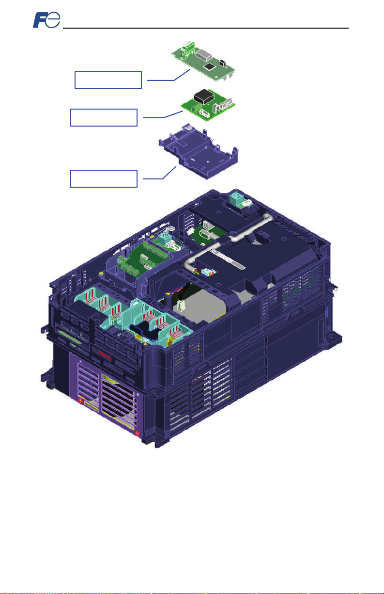
• OPC-PRT inter face b oar d wit h spac er an d captive M3 x 12mm s crew in l ower-right corner (r ef er t o
Figure 1).
• One s ep arate M3 x 6mm mounting screw (see Figur e 2).
• Type A m ale to m ini-B male USB interface cable (see Figur e 3).
Figure 2: M3 x 6mm Mounting Screw
Figure 1: OPC-P RT Interf ace Board
Figure 3: USB Interface Cable
14
Standoff m ounting hole
Inv ert er contr ol
USB port
Module Status LED
Spacer and c aptive screw
MAC Address
Port 1 Ethern et j ack
Port 2 Ethern et j ack
Positioning notch
1.3.2 Component Overview
Figure 4 prov ides an overview of th e impor ta nt i nt erf ac e car d c omponents.
board connector
Networ k Stat us LED
Port 1 Link/Activity LE D
Port 2 Link/Activity LE D
Positioning Notch
Aligns with the positioning key on the invert er chassis to ensure that the interface card is installed into
the correc t c omm unicati on p ort (r efer t o sec ti on 2.2).
Port 1 and Port 2 Ethernet Jacks
Either jack can freely b e used in star topology networks (with external switch). In linear topologies, a
series of cards can be c onnected t ogether by daisy-chaining one of the ports to the next inverter in line.
In ring topologies, MRP (Media Redundancy Pr otocol) must be supported by all devices on the network.
Standoff Mo unting Hardw are
The provided M3 x 12mm and M3 x 6mm screws ar e used to s ecure the car d t o th e st and offs loc ated on
the inverter’s control board. Ref er to s ection 2.2.
Inverter Control Board Connector
Att ach es t o the invert er’ s connector board, which m ay vary depending on the inverter model.
USB Port
USB 2.0 port with mini-B con nec tor. Use d to acc ess the card via t he Fuj i Configuration Studio ( ref er to
section 5) an d as a USB f lash dr ive (r efer t o s ect ion 7).
Module Stat us and Netw ork Status LEDs
Thes e L EDs indic at e th e curr ent status of the int erfac e c ard and pr otoc ols in us e. R ef er t o section 1.4.
Ethernet Link and Activity LEDs
One s et of L EDs ar e pr ovided for each E thernet por t. These LEDs provid e ins ight i nt o th e Et her net
network’s status and activity. Refer to section 1.4.
Figure 4: OPC-P RT Component Overview

15
LED Activ ity
Status
Note
Off
Dev ice Off
The inv ert er pow er is of f
Green Blink /
Red Blink
Green Blink
No Connection
Eth erN et/ IP con nection is n ot es t abl ish ed
Green Off
No Connection
PROFINET c onnection is not established
Con nec ti on
Established
LED Activ ity
Status
Note
Off
Dev ice Off
The inv ert er pow er is of f
Green Blink /
Red Blink
Green On
Dev ice On
Normal st atus
Discov ery
identification
Rec ord th e err or code s equ enc e and c ont act
technical support
LED Activ ity
Status
Note
A valid Ethernet link exists: commu nic at ion is
possible on this port
A valid Ethernet link does not exist: communication is
not possible on this por t
Indicates when a pac ket is tr ans mit ted or rec eived on
this port
1.4 LED Indicators
1.4.1 Standard LEDs
1.4.1.1 Network Status LED
Startup Startup blink sequenc e
Green On
1.4.1.2 Module Status LED
Startup Startup blink sequenc e
Green Blink
Red Blink Error Code
1.4.2 Ethernet Link/Activity LEDs
Green On Link
Green Off No L ink
Red Blink Activity
Eth erN et/ IP or PROFI NET connect ion is est ablish ed
PROFIN ET discovery and identification (DCP)

16
Bef ore installing th e interf ace car d, perfor m all wiring for the main circuit terminals and
control circ uit terminals.
2 INSTALLATION
2.1 Pre-Installation Instructions
• To avoid el ect rical sh ock , r emove all pow er f rom th e in ver ter an d w ait at leas t f iv e minutes prior t o
starting installation. Additionally, confirm that the DC link bus volt age as measur ed between the P
(+) and N (-) terminals is less than 25 VDC.
• Installation should be performed only by qualified personnel.
• To avoid electrical sh ock, do not operate the inverter with the front cover or wiring cover removed,
as accident al contact with expos ed high-voltage terminals and internal c omponents may occur.
• To prevent explosions or similar damage, ens ure that all cables are properly connected t o the
correc t termi nals, and observe all wir ing pol arity indicat ors.
• Only one additional opt ion card m ay be used when the OPC-PRT is installed in the inverter. If
two additional option c ards are required, p lease consult with the factory first to confirm
compatibility.
2.2 Installation Procedure
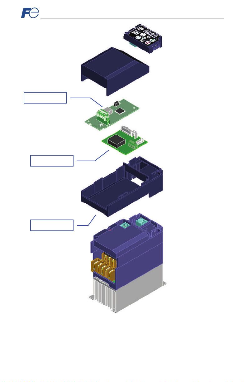
1. Remove the front cover from the invert er to expose the contr ol print ed circuit board (control PCB).
Install th e interf ac e car d according to t he inv ert er cap acity as shown in Figur e 5, Figur e 6, or
Figure 7. Ot her wise, r efer to the FRENIC-ACE Instruction Manual or c ontact Fuj i for the
appropriat e installation instructions.
T o remove the front c over, ref er t o th e FREN IC-Ac e Instruction Manual, Section 2.2.
17
Int erf ac e Car d
Con nec tor Board
Option Case
Figure 5: Installation for 15 kW and Smaller Inverters
18
Int erf ac e Car d
Con nec tor Board
Option Case
Figure 6: Installation for 18.5 kW to 22 kW Inverters
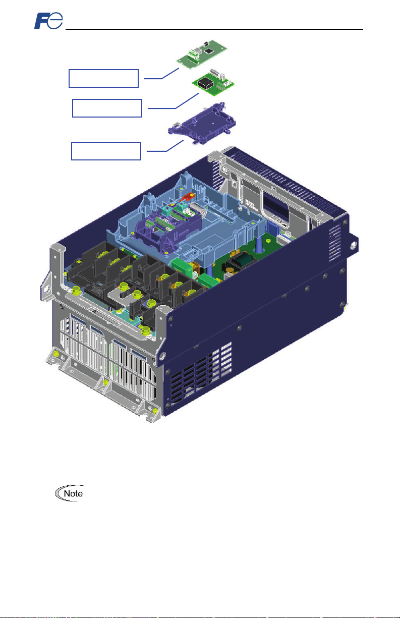
19
Ensure that the interface card is fully aligned and seated into the communication
cont act f ail ur e.
Int erf ac e Car d
Con nec tor Board
Option Case
Figure 7: Installation for 30 kW and Larger Inverters
2. Engag e c onn ect or CN1 (on th e back of the interf ace car d) int o the connec tor on th e c onn ect or
boar d. Ens ur e th at t he c on nec tors are f ul ly engaged.
port. Failure to do so may lead to ins ufficient con nec tor ins ertion and r esult in
3. Secure the int erfac e c ard to t he c on nec tor board PCB by first tightening the captive M3 x 12mm
screw into the inver ter standoff locat ed at t he low er-rig ht h and corn er of the interf ace car d. Next ,
install and tight en the included M3 x 6mm s cr ew into the st and off mounting hole located at the
upper-left hand c orn er of th e interf ace card.
4. Connect the network cables as nec essar y. Ins ert th e Et hernet c abl es i nt o th e Et her net jacks,
mak ing sure t hat th ey are f ull y s eat ed. Ensur e that the cables are rout ed in such a way that they

20
will not be pinched and are not located near any power-c arrying wiring, such as the inverter ’s input
pow er or motor wires .
5. Reinstall all covers r emoved in step 1. Tak e a m om ent to c onf ir m that the Ethernet cables ar e not
being pinch ed and ar e not routed near any power-carrying wiring.
For reinstallation instructions, refer to the FRENIC-Ac e Instruction Manual, S ection 2.2.

21
For fur th er d etails regar ding t hes e function codes, pl eas e r ef er t o the FRENIC-Ace
(24A7-E-0082), Chapter 5, Section 5.2 "Data Formats."
Setting
Range
Required
Val ue
Y98
Bus Link Function (Mode Selection)
0 to 3
3
S## Function Code
Hierarchy Prior ity
Description
S01
Highes t
frequency refer enc e / per -unit
S05
2nd Hi ghest
frequency refer enc e / Hz
S19
3rd Hig hes t
speed command
S02
4th Highest
torque com mand
S03
5th Highest
torque cur rent c ommand
S13
Low est
PID c omman d
3 INVERTER FUNCTION CODE SETTINGS
Depending on the desired operation of the overall applicat ion, the inv ert er function codes listed in Table
11 are important for prop er operation of the end-to-end communication system. Although there may be
man y oth er function codes that will require c onfiguration for your specific application, it is import ant to
understand the manner in which the following function codes will impact successful control of the
inv ert er.
Instruction Manual (INR-S I47-1733a-E), Chapter 5 "FUNCTION CODES", FRENIC-Ace
User’s Manua l (24A7-E-0043E), “ y codes : Link Functions”, and RS-485 User's Manual
Table 11: Function Code Settings Overview
Code Name
3.1 Inverter Control-Related Settings
The following function codes relate to whether or not the inverter is to be contr olled (command word
and/or fr equency command) f rom th e network , or wheth er t he inverter will be locally-controlled (and
theref or e only m onitored and/or configured via the network.)
Bus Link Funct ion (Mode Selection) (y98)
If t he i nvert er is to be c ontr olled from th e network, then s et the val ue of y 98 to 3 (fieldbus option). A
setting of 3 for y98 may also be appropriate even if H30 is c onfigur ed for an alt ernate (local) contr ol
scheme.
When the inver ter is controlled from the network, a sel ect ion of refer enc e commands (S## function
codes as defi ned in Table 12) are available for controlling the inverter’s speed. If mu ltipl e r efer enc e
comm an ds are being modified from the netw ork , t hen th e int erfac e c ard in vok es a hi erarchy t o
det erm ine wh ich refer enc e is to be p ass ed to the i nvert er as it s m ain r efer enc e c omm an d.
The S ## function code hier arch y is lis ted fr om h ig hes t t o lo wes t prior it y in T ab le 12.
Table 12: S## Function Code Hierarchy
The highest-priority S## function code with a non-z ero va lue will be us ed as the invert er’ s main
referenc e command.

22
o27 Value
o28 Value
Inverter r eaction w hen a timeout occurs
Remarks
0,
4 to 9
0.0s to
60.0s
Aft er t he t im e sp ec ifi ed b y o2 8, coas t t o a s to p
and trip
.
If t he c omm un icati ons lin k is restored with in the
to a stop and trip
.
3,
13 to 15
Maintain pr esent oper ation, ignoring the
comm un ic ati ons error (n o er5 trip).
Inv ert er function cod e
dec elerat ion time
0.0s to
60.0s
Aft er t he t im e sp ec ifi ed b y o2 8, dec el erat e t o a
stop. Trip er5 af ter stopping.
If t he c omm un icati ons lin k is restored with in the
dec elerat e t o a stop an d tr ip er5.
For det ails r egarding the int erfac e-sp ecific tim eout behavior and configuration, pleas e refer
to s ect ion 5.4.1.
3.2 Inverter Reaction to Network Timeout Conditions
Function c odes o27 and o28 specify the inverter’s reaction when a network timeout occurs . Tab le 13
lis ts the sett ings f or o27 and o28.
Table 13: Inverter Reaction to Network Timeout Conditions (Function Codes o 27 and o28)
--- Immediately coast to a stop and trip er5.
1
2
10 ---
11
12
0.0s to
60.0s
---
0.0s to
60.0s
er5
time specified by o28, ignore the
communications error. After the timeout, coast
er5
Immediately decelerate to a stop. Trip er5 after
stopping.
time specified by o28, ignore the
communications error. After the timeout,
F08 sp ecifies the
Sam e as abov e
Sam e as abov e

23
( )
1 number offset 256 x number groupregister ++=
( )
2058 1 9 256 x8 =++
4 FUNCTION CODE NUMBERING AND BEHAVIOR
4.1 Register Numbers
All accessible invert er function codes c an be referenc ed by their Modbus reg ister indices , as defined in
the RS-485 User’s Manual (24A7-E-0082), section 3 (Table 3.2) and can be conveniently r eferenc ed in
the configuration studio (section 5. 6) and the em bedded web server (section 6.2.3). Thes e s ame r eg ister
numb ers are us ed w hen acc es sin g f unc ti on c odes via c ert ai n Et her net pr ot ocols. Th e terms “function
code” and “register” refer to data stored on the inverter and will be used interchangeably thr oughout this
documentation. The max support ed register number is 13668. Because the RS-4 85 User’s Manual
contains inf ormation for several Fuji inverter families, the relevant information will be paraphrased here
for the specific cas e of th e FRENIC-Ac e.
All inv ert er f un ct ion codes are exp os ed as r egist er in dic es accor ding t o a m athematical conv ers ion
formula which combines two elements (a function code group number and function code offset) to create
a unique register number for each fu nction code. Each function code group (“E” / Extension Terminal
Functions, for examp le) is assigned a specif ic function code group number (r efer to Table 14). Each
function code also has an offset number, which is the function code without the leading l ett er ( th e offset
number for function code E05, for example, is 5). To determine the register number for a given function
code, therefore, the gr oup number is first multiplied by 256, then added to the offset number plus 1. This
operation is express ed mathemat ic al ly vi a Equation 1.
As an example, let’s calculate the register number for output frequency (function code M09). According
to T able 14, the group num ber for the “M” function code group is 8. It is also evident that the offset
number for M09 is 9. Ins erting the group number and offset number int o Equation 1, we arr iv e at th e
result indic at ed in Equation 2.
While manually calcu lating all of the register numbers for the function codes of interest is cert ainly
possible by us ing Equation 1, it m ay be more convenient to simply reference the “Register” column on
the mon itor t ab of th e default web int erfac e (ref er to section 6.2.3).
Not e th at n ot all of t he availabl e regis ters that exist in t he int erf ac e card’ s r egist er m ap have
corresponding function codes th at exist in the invert er. In oth er w or ds, if a read from or writ e t o a r egist er
num ber th at d oes not cor respond to an exist in g inver ter function c od e tak es pl ace, the r ead/wr it e may b e
successful (depending on the specific register accessed; refer to section 4.2) , but t he d ata will h ave no
meaning. This feature is beneficial in situations where the accessing of non-con tiguo us reg ister s c an be
made more efficient by accessing an all-i nclus ive bl ock of r egist ers (s ome of w hich c orr espond to
inv ert er function cod es and s om e of wh ich do not), w hile only manipulating those in your local
programming that are kn own to exist.
Equation 1
Equation 2

24
Function Code Group
Code
Name
F00: (0 x 256) + 0 + 1 = 1
F99: (0 x 256) + 9 9 + 1 = 100
E00: (1 x 256) + 0 + 1 = 257
E99: (1 x 256) + 99 + 1 = 356
C00: (2 x 256) + 0 + 1 = 513
C99: (2 x 256) + 99 + 1 = 612
P00: (3 x 256) + 0 + 1 = 769
P99: (3 x 256) + 99 + 1 = 868
H00: (4 x 256) + 0 + 1 = 1025
H99 (4 x 256) + 99 + 1 = 1124
A00: (5 x 256) + 0 + 1 = 1281
A99: (5 x 256) + 99 + 1 = 1380
o00: (6 x 256) + 0 + 1 = 1537
o99: (6 x 256) + 9 9 + 1 = 1636
S00: (7 x 256) + 0 + 1 = 1793
S99: (7 x 256) + 99 + 1 = 1892
M00: (8 x 256) + 0 + 1 = 2049
M99: (8 x 256) + 9 + 1 = 2148
r00: (10 x 256) + 0 + 1 = 2561
r99: (10 x 256) + 99 + 1 = 2660
Table 14: Function Code-to-Register Conversion Examples
F
E
C
P
H
A
Fundamental
Functions
Extension
Termin al
Functions
Control
Functions
Mot or 1
Par ameter s
High
Perfor man ce
Functions
Mot or 2
Par ameter s
Gro up
Numb er
0
1
2
3
4
5
Register Example Using Equation 1
:
F07 (acceleration time 1): (0 x 256) + 7 + 1 = 8
:
:
E98 (terminal [FWD] function): (1 x 256) + 98 + 1 = 355
:
C20 (jogging frequency): (2 x 256) + 2 0 + 1 = 533
:
:
P03 (motor 1 r ated current): (3 x 256) + 3 + 1 = 772
:
:
H11 (deceleration mod e): (4 x 256) + 11 + 1 = 1036
:
:
A05 (motor 2 t orque boost): (5 x 256) + 5 + 1 = 1286
:
Oper at ional
o
Functions
Command
S
M Mon it or D at a 1 8
r
Dat a
Mot or 4
Par ameter s
o01: (6 x 256) + 1 + 1 = 1538
6
:
:
7
S05 (frequency comman d): (7 x 256) + 5 + 1 = 1798
:
:
M09 (output frequency): (8 x 256) + 9 + 1 = 2058
:
:
r02 (motor 2 base frequency): (10 x 256) + 6 + 1 = 2563
10
:

25
Function Code Group
Code
Name
Customizable
Functions
U00: (11 x 256) + 0 + 1 = 2817
U99: (11 x 256) + 99 + 1 = 2916
J00: (13 x 256) + 0 + 1 = 3329
J99: (13 x 256) + 99 + 1 = 3428
y00: (14 x 256) + 0 + 1 = 3585
y99: (14 x 256) + 99 + 1 = 3684
W00: (15 x 256) + 0 + 1 = 3841
W99 (15 x 256) + 99 + 1 = 3940
X00 (alarm history / latest): (16 x 256) + 0 + 1 = 4097
X99: (16 x 256) + 99 + 1 = 4196
Z00: (17 x 256) + 0 + 1 = 4353
Z99: (17 x 256) + 99 + 1 = 4452
b00: (18 x 256) + 0 + 1 = 4609
b99: (18 x 256) + 99 + 1 = 4708
d00: (19 x 256) + 0 + 1 = 4865
d99: (19 x 256) + 99 + 1 = 4964
W100: (22 x 256) + 0 + 1 = 5633
W199 (22 x 256) + 99 + 1 = 5732
W200: (23 x 256) + 0 + 1 = 5889
W299 (23 x 256) + 99 + 1 = 5988
o100: (37 x 256) + 0 + 1 = 9473
o199: (37 x 256) + 99 + 1 = 9572
Customizable
Functions
U100: (39 x 256) + 0 + 1 = 9985
U199: (39 x 256) + 99 + 1 = 10084
Gro up
Numb er
U
J
y Link Functions 14
W Monitor Data 2 15
X Alarm Data 1 16
Z Alar m D at a 2 17
b
Logic
Application
Functions 1
Mot or 3
Par ameter s
11
13
18
Register Example Using Equation 1
:
:
J03 (PID proportional gain): (13 x 256) + 3 + 1 = 3332
:
:
y98 (bus link function): (14 x 256) + 98 + 1 = 3683
:
W32 (PID output): (15 x 256) + 32 + 1 = 3873
:
:
:
rd
last alarm torque): (17 x 256) + 53 + 1 = 4406
Z53 (3
:
:
b12 (motor 3 starting frequency): (18 x 256) + 12 + 1 = 4621
:
Application
d
Functions 2
W1 Monit or D at a 3 22
W2 Monit or D at a 4 23
Oper at ional
o1
Functions
U1
Logic
19
37
39
:
d24 (zero speed contr ol): (19 x 256) + 24 + 1 = 4889
:
:
:
:
:

26
Function Code Group
Code
Name
J100: (48 x 256) + 0 + 1 = 12289
J199: (48 x 256) + 99 + 1 = 12388
J1 PID Control 1 48
Gro up
Numb er
:
Register Example Using Equation 1
4.2 Scanned Function Codes
The interface card provides netw ork access to the specified list of function codes contained in the
param.xml file located in the “WEB” fo ld er of th e inter face c ard’s file syst em. Th ese funct ion codes are
constantly being read and/or written (as applicable), and t heir c urrent values ar e ther efore mirror ed in
the int erfac e card’ s i nt ern al m em ory. Only those function c odes specified in the param.xml file will
represent meaningfu l values.
The principle disadvantage of sc anned function codes is that writ e data checking is not available. This
means that when the value of a scann ed function code is modified via a network protocol or via the web
brows er’s monit or tab, t he interf ac e car d it self is n ot able to det ermine if the new va lue will be acc epted
by the invert er ( th e value may be out-of-r an ge, or the inverter may be i n a s tat e in wh ich it wil l not accept
new values being writt en via commu nications, etc.) For exam pl e, if a w rit e is perf orm ed t o a s canned
command function c ode wit h a dat a valu e th at is out-of-range, th e interf ace car d w ill not gener ate a
corres ponding err or. Howev er, if end-to-end confirmation of such data writes is required, then the
function code can be read ov er th e net work at a lat er tim e to confi rm that th e wr itten val ue “ took h old” i n
the inv ert er.
Accesses to any function c ode (?00…?99, where “?” is any v alid function code gr oup letter from Tabl e
14) will always be successful. Even if an inverter function code corresponding t o a given register does
not exist in the param.xml file, the interface card still maintains a placeholder location in its int ernal
mirroring m emory for that function code. This feature allows for the block access of non-contiguous
registers (funct ion cod es) as described in s ection 4.1. Care m ust be tak en t o ut iliz e on ly t he f unction
codes that are kn own to exist and t hat ar e also specif ied in th e param.xml file.
4.3 Commonly Used Function Codes
For a complete listing of all available function codes, their bit mappings, scaling values, etc., please refer
to the Fuji FRENIC-Ace Instruction Manual (INR-SI47-1733a-E) and the Fuj i RS-485 User’s Manual
(24A7-E-0082). As a user conv enience, th e st ructures of the com monly-used “Operation c ommand”
(function code S06), “Operation status” (function c ode M14) and “ Rotation Speed” (function code W08)
are r ep lic at ed h ere (r efer t o Table 15, Tabl e 16 and Table 17, res pec tivel y).
Table 15: Structure of “Operation comm and” (Function code S06)

27
Table 16: Structure of “Operation status” ( Function co de M14)
Table 17: Structure of “Rotation Speed” (Function code W08)
28
5 FUJI CONFIGURATION STUDIO
5.1 Overview
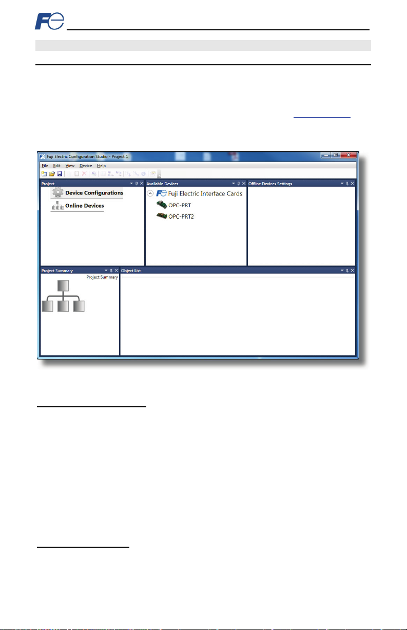
The interface card is discovered, configur ed and updated by the Fuj i Configuration Studio PC application
(refer to Figure 8). Th e st ud io m ust be installe d pr ior to c on nec ti ng an interf ace car d t o th e computer in
ord er t o ensur e that the ap pr opr iat e USB driv ers ar e inst alled. Th e st udio typically r equir es a USB
connection f or reading/writing a configur ation and updating the firmware. Depending on the currentlyactive dri ver s, remote d iscovery, network setting, configur ation, and firmware updates are als o possibl e
via Eth ernet. To obt ain th e lates t r el eas e of the Configuration Studio, ref er t o the pr oduct web page
the int ernet or c ont act technic al s up por t. The r emainder of th is sec tion will provide only a br ief
introduction to the c onfiguration concepts. For protocol specific configuration, r efer to the relevant
protocol section.
on
Figure 8: Fuj i Configuration Studio
Creating a Device Configuration
A dev ic e c an b e added to t he Project p anel for configuration by first selecting the Device
Configurations list heading and then:
• Dou ble -clicking on the device in the Available Devices panel.
• Right-click ing on the device in the Available Devices panel and choosing Add fr om the cont ext-
sensitive menu.
• Hitting the <ENTER> key on the keyboard when the device is s elected in th e Available Devices
panel.
• Dragging the device fr om the Available Devices panel into the Project panel.
• Selecting it and selecting Add Selected Device fr om t he E dit menu.
• Selecting it and clicking the Ad d button in the toolbar.
The d ev ic e wi ll t hen be add ed t o the l ist of Device Configurations.
Going Online w ith a Device
All con nec ted de vic es ar e aut om atically added to t he D iscovered Devices panel. This panel is shown
by sel ect in g the Online Devices list heading in the Project panel. To go online with a device:
• Dou ble -clic k on it in the Discovered Devices panel.

29
• Right-clic k on it in the Discovered Devices p anel and c hoose Go Online from the context-
sensitive menu.
• Hit the <ENTER> key on the keyboard wh en the devic e is selected in the Discovered Devices
panel.
• Drag it from the Discovered Devices panel into the Project panel.
• Sel ect it and sel ect Go Online with Device fr om t he Edit menu.
• Select it and click the Go Online button in the toolbar.
When the studio goes online with a device, its configuration is automatically read. W hile the studio is
online with a device, it will appear in green text in the Discovered Dev ices panel. The studio may be
online with multiple dev ices simultaneously.
Uploading a D evice’s Configuration into a Project
The current configur ation of an online device can be uploaded into the Project panel by selecting a
device under the Online Devices list heading and th en:
• Right-click ing on it and choosing Upload Configuration from the c ont ext -sensit ive menu.
• Dragging it from the Online Devices heading into the Device Configurations heading.
• Selecting it and selecting Upload Configuration to Project from th e Device menu.
• Selecting it and clicking the Upload Configuration button in the toolbar.
The device’s configur ation will then be added to the list of Device Co nfigurations. Onc e th e
configuration is uploaded into the project, it may be modified.
Removing a Device Configuratio n from a Project
A configur at ion can be rem oved from a pr oj ect by:
• Selecting the device in the Project panel and dragging it. A trash can icon will appear at the
bottom of t he Project p anel, and dr agging and dropping the device in the trash will remov e it from
the projec t.
• Hitting the <DELETE> k ey on the keyboard when the devic e is selected in the Project panel.
• Right-click ing on the device in the Project panel and choosing Remove from the context-s ensit ive
men u.
• Selecting Remove Selected Item f rom the Ed it menu when the device is select ed.
• Clicking on the Rem ove butt on in the toolbar when the device is selected.
Going Offline with a Device
To go of flin e wit h a device:
• Sel ect th e devic e in th e Project panel and drag it. A trash can icon will appear at the bottom of the
Project panel, and dr agging and dr opping the device in the trash will go offline with it.
• Hit the <DELETE> key on the keyboard when the device is selected in the Project p anel.
• Right-click on the devic e in the Project panel and choose Go Offline from the context-sensitive
men u.
• Sel ect Go Offline w ith Device from the Edit menu when the device is selected.
• Click on the Go Offline button in the toolbar when the device is selected.
Downloading a Configuration to a Device
To download a configur at ion to an online device, first selec t t he d ev ic e under the Device
Configurations heading in the Project panel, and then navigat e to Device…Download Configurat ion
to Device. If the studio is currently online with only one compatible device, then the configu ration will be
downloaded t o the online device. Otherwis e, a device selection pr ompt is displayed to select which
device to d own lo ad t he configur ation to. Do n ot pow er off the dev ic e or int errup t the c onnectio n once the
download is in progress as this may corrupt the firmware and/or the configuration.
Stop all other communication to the device when download ing.
 Loading...