

Page 1
Instruction Manual
t
A
Availabl
PG Interface (5 V Line Driver) Card "OPC-G1-PG22"
Thank you for purchasing this PG interface card containing 5 V line driver card (hereinafter called PG interface card), "OPC-G1-PG22."
Mounting this card on your FRENIC-MEGA enables synchronous operation of two motors using PGs or frequency command entry by
pulse train input.
Mounting this interface card disables the pulse train input function assigned to the inverter's [X7] terminal.
The FRENIC-MEGA has three option connection ports--A-, B-, and C-ports. Connect this PG interface card to the C-port.
The A- and B-ports cannot accept this card. Mounting this card occupies also the B-port space so that any option card canno
be connected to the B-port.
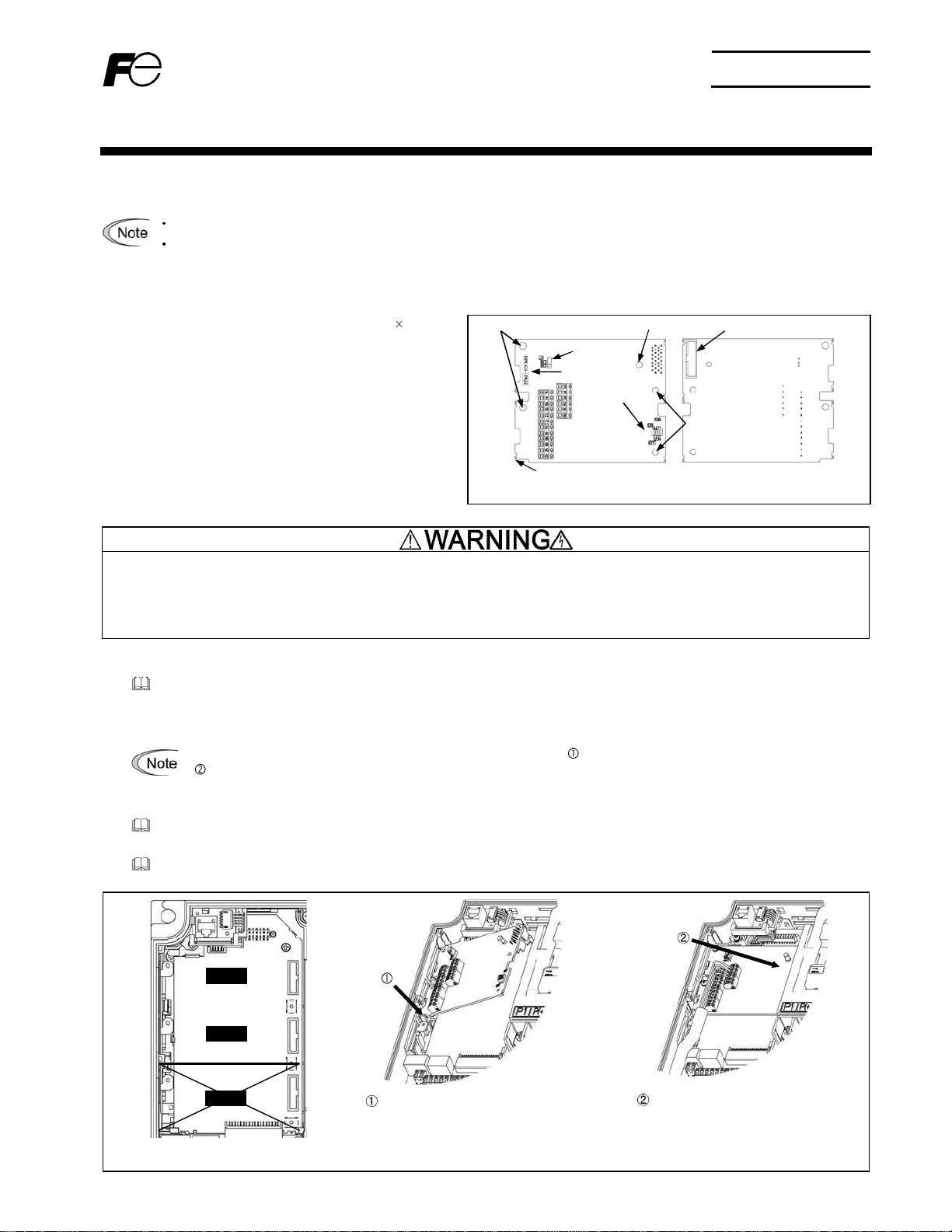
1 Check that:
(1) A PG interface card and four screws (M3 8) are
contained in the package.
(2) The PG interface card is not damaged during
transportation--no defective devices, dents or warps.
(3) The model name "OPC-G1-PG22" is printed on the PG
interface card. (See Figure 1.1.)
If you suspect the product is not working properly or if you
have any questions about your product, contact the shop where
you bought the product or your local Fuji branch office.
2 Installation
Screw holes (left)
Model name
Positioning cutout
Figure 1.1 Front of Card Figure 1.2 Back of Card
Release knob
J1
SW1
CN1
Screw holes (right)
Before starting installation and wiring, turn OFF the power and wait at least five minutes for inverters with a capacity of 22 kW or
below, or at least ten minutes for inverters with 30 kW or above. Make sure that the LED monitor and charging lamp are turned OFF.
Further, make sure, using a multimeter or a similar instrument, that the DC link bus voltage between the terminals P(+) and N(-) has
dropped to the safe level (+25 VDC or below).
Otherwise, electric shock could occur.
(1) Remove the front cover from the inverter and expose the control printed circuit board (control PCB). The PG interface card can be
connected to the C-port (CN6) only. (Figure 2.1)
To remove the front cover, refer to the FRENIC-MEGA Instruction Manual, Section 2.3. For inverters with a capacity of 30 kW or
above, open also the keypad enclosure.
(2) Insert connector CN1 on the back of the PG interface card (Figure 1.2) into the C-port (CN6) on the inverter's control PCB. Then
secure the card with the four screws that come with the card. (Figure 2.3)
Check that the positioning cutout (Figure 1.1) is fitted on the tab ( in Figure 2.2) and connector CN1 is fully inserted
( in Figure 2.3). Figure 2.3 shows the PG interface card correctly mounted. Do not connect the interface card to the
ports other than C-port. Doing so may damage the card.
(3) Perform wiring to the PG interface card.
Refer to Section 3 "Wiring."
(4) Put the front cover back into place.
To put back the front cover, refer to the FRENIC-MEGA Instruction Manual, Section 2.3. For inverters with a capacity of 30 kW or
above, close also the keypad enclosure.
C-Port
e
(B port also
occupied)
B-Port
CN6
CN5
-Port
Not available
Figure 2.1 Option Connection Ports
CN4
Fit the positioning cutout of the card over
the tab on the inverter to determine the
mounting position.
Figure 2.2 Mounting PG Interface Card Figure 2.3 Mounting Completed
- 7 -
Insert connector CN1 on the card into
the C-port (CN6) on the inverter's
control PCB.
Page 2
3 Wiring
In general, the covers of the control signal wires are not specifically designed to withstand a high voltage (i.e., reinforced insulation is
not applied). Therefore, if a control signal wire comes into direct contact with a live conductor of the main circuit, the insulation of the
cover might break down, which would expose the signal wire to a high voltage of the main circuit. Make sure that the control signal
wires will not come into contact with live conductors of the main circuit.
Failure to observe these precautions could cause electric shock or an accident.
Noise may be emitted from the inverter, motor and wires.
Take appropriate measures to prevent the nearby sensors and devices from malfunctioning due to such noise.
An accident could occur.
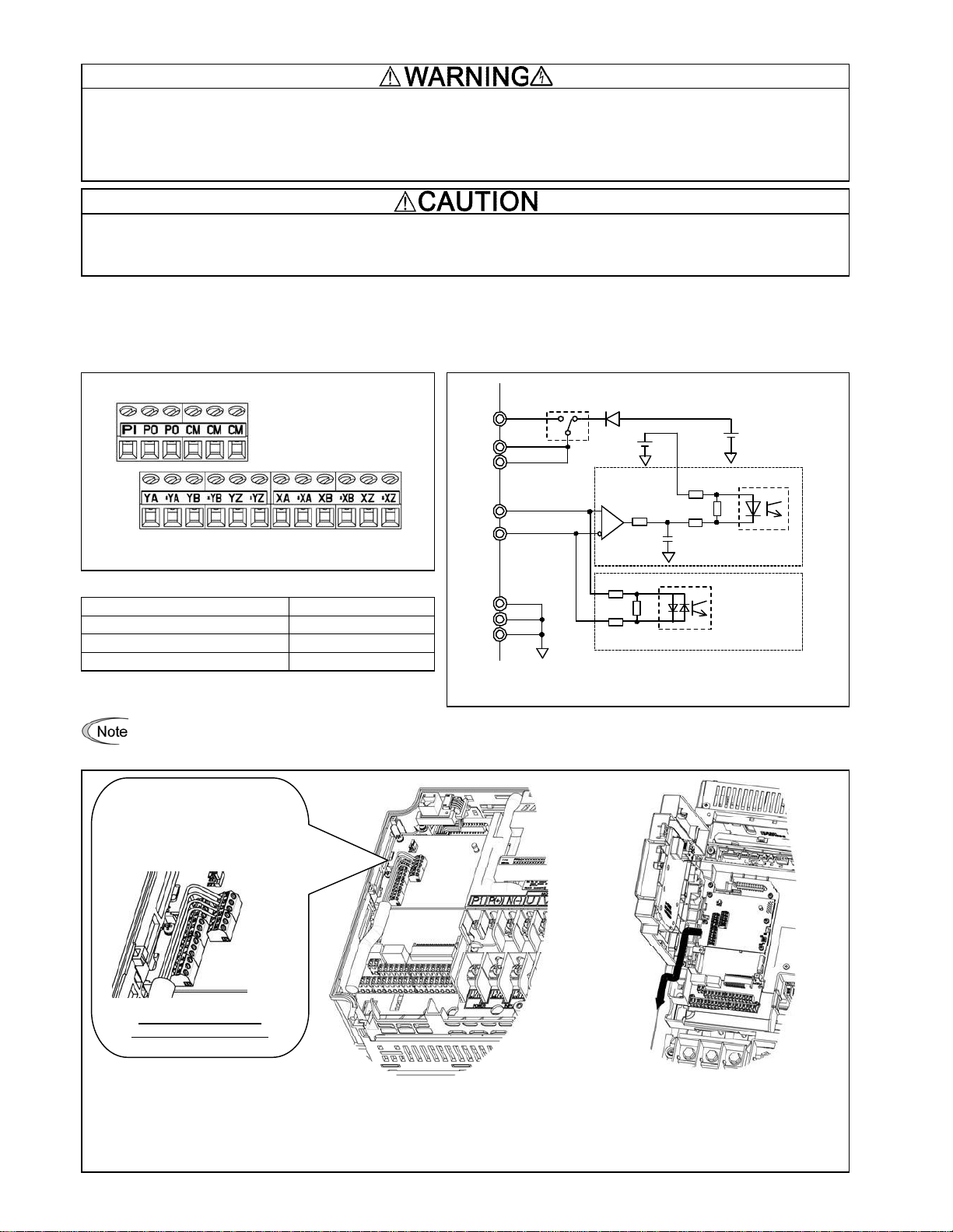
Perform wiring to the PG interface card, referring to the "Terminal Allocation and Symbol Diagram" (Figure 3.1), "Terminal
Specifications" (Table 3.1), "Internal Block Diagram" (Figure 3.2), and "Wiring Instructions" (Figure 3.3) given below.
For wiring between the PG interface card and the PG(s), use a shielded cable having a length of 100 m or below. It is recommended that
the shielded layer be connected to the [CM] terminal on the card and be open at the PG side. If malfunctioning due to noise causes a
problem, winding the shielded cable around a ferrite core by one or two turns may reduce the problem.
J1
PI
PO
PO
YA, YB, YZ,
XA, XB, XZ
INTEXT
+5 VDC
+5 VDC
Photocoupler
Figure 3.1 Terminal Allocation and Symbol Diagram
Table 3.1 Terminal Specifications
Terminal Size M2
Tightening Torque 0.22 to 0.25 N·m
Recommended Wire *1 AWG16 to 24
Wire strip length 6 to 7 mm
1
*
Insulated wires with allowable temperature of 105ºC (UL-listed)
are recommended.
To prevent malfunctioning due to noise, separate the wires of the interface card as far apart as possible from those for the main
circuits. Also, inside the inverter, bundle and fix the wires of the interface card so that they do not come into direct contact with
the main circuit terminal block or other live parts of the main circuits.
Connect the shielded layer to a
[CM] terminal.
If [CM] terminals are lacking, share
a single terminal with two wires and
tighten them together.
*YA, *YB, *YZ,
*XA, *XB, *XZ
CM
CM
CM
Figure 3.2 Internal Block Diagram
Photocoupler
I/F circuit
Wire break
detection circuit
Connecting the cable to
terminals (magnified view)
In the case of 7.5 kW In the case of 75 kW
Pass the wires from the PG interface cardbetween
the control circuit terminal block and the front cover.
Figure 3.3 Wiring Instructions
- 8 -
Page 3

4 Specifications
Table 4.1 lists the specifications of the PG interface card.
Table 4.1 PG Interface Card Specifications
Item Specifications
Pulse resolution 20 to 3000 P/R
Maximum response frequency 100 kHz
Applicable PG
Pulse output system Line driver (Equivalent to 26C31 or 26LS31)
Source current: +20 mA (max.), Sink current: -20 mA (max.)
Maximum wiring length 100 m
PG power supply +5 VDC 10%, 300 mA or below *
1
*
When the PG current consumption exceeds 300 mA, use an external power supply.
1
5 Terminal Functions
Table 5.1 lists terminal symbols, names and functions of the option terminals on the PG interface card.
Table 5.1 Option Terminals and Their Specifications
Terminal symbol Name Functions
Power input terminal from the external device for the PG
PI External power supply input*
1
+5 VDC 10% input *
(A power supply to be connected should assure the PG current consumption or
larger.)
PO Internal power supply output*
Power supply
CM PG power common *
4
5
Power output terminal for the PG
+5 VDC -0% to +10%, 300 mA output *
Common terminal for power supply for PG
(Equipotent with [CM] terminal of the inverter)
YA YA(+) phase pulse input from slave PG Input terminal for A(+) phase signal fed back from the slave PG
*YA YA(-) phase pulse input from slave PG Input terminal for A(-) phase signal fed back from the slave PG
YB YB(+) phase pulse input from slave PG Input terminal for B(+) phase signal fed back from the slave PG
*YB YB(-) phase pulse input from slave PG Input terminal for B(-) phase signal fed back from the slave PG
YZ YZ(+) phase pulse input from slave PG Input terminal for Z(+) phase signal fed back from the slave PG
*YZ YZ(-) phase pulse input from slave PG Input terminal for Z(-) phase signal fed back from the slave PG
XA XA(+) phase pulse input from reference PG Input terminal for A(+) phase signal fed back from the reference PG
PG/pulse input
*XA XA(-) phase pulse input from reference PG Input terminal for A(-) phase signal fed back from the reference PG
XB XB(+) phase pulse input from reference PG Input terminal for B(+) phase signal fed back from the reference PG
*XB XB(-) phase pulse input from reference PG Input terminal for B(-) phase signal fed back from the reference PG
XZ XZ(+) phase pulse input from reference PG Input terminal for Z(+) phase signal fed back from the reference PG
*XZ XZ(-) phase pulse input from reference PG Input terminal for Z(-) phase signal fed back from the reference PG
*1 When the PG current consumption exceeds 300 mA, use an external power supply and set a jumper cap at the EXT side on jumper J1. (Refer to
Section 6 "Configuration".)
2
*
Use an external power supply whose rating meets the allowable voltage range of the PG. Regulate the external power supply voltage within the PI
voltage range (upper limit +10%), taking into account the voltage drop caused by the PG-inverter wiring impedance. Or, use a wire with a larger
diameter. (Refer to Table5.2)
3
*
If the PO voltage level falls below the allowable voltage range of the PG due to voltage drop caused by PG-inverter wiring impedance, use an
external power supply or a wire with a larger diameter.
4 *5
*
The PG interface card has two [PO] terminals and three [CM] terminals, each of which is conducting inside the card.
2
3
PG power supply
requirements
5 V 10% 300 mA
Table 5.2 Recommended Wire Size
Wiring length (m)
Up to 20 Up to 30 Up to 50 Up to 75 Up to 100
AWG24
(0.25 mm2)
AWG22
(0.34 mm2)
- 9 -
AWG20
(0.50 mm2)
AWG18
(0.75 mm2)
AWG16
(1.25 mm2)
Page 4

6 Configuration
6.1 Switching between internal and external power supplies for PGs
Before powering on the inverter, switch between internal and external power supplies for the PGs using jumper J1, referring to Table 6.1
and Figure 6.1.
Table 6.1 Internal and External Power Supplies for PGs
Power Supply Short-circuit jumper J1 using a jumper cap
Internal power supply
(Factory default)
External power supply
At the INT side
(Use the power supply with max. 300 mA load current.)
At the EXT side
Connect +5 VDC 10% power to the [PI] terminal.
When using an internal power supply When using an external power supply
(Factory default)
Figure 6.1 Configuration of Jumper J1
6.2 Enabling/disabling the wire break detection function with DIP SW1
The PG interface card has a wire break detection function that detects wire breaks in the PG cable. It is possible to enable/disable this
detection function in each of the YZ, XA, XB, and XZ phases. Please refer to Table 6.2 when enabling/disabling the detection function
for each phase with the DIP SW1.
Note that the wire break detection function of the YA and YB phases is always enabled. When not using these phases, connect their
respective (+) phases to the [PO] terminals and their respective (-) phases to the [CM] terminals.
Table 6.2 Enabling/Disabling the Wire Break Detection Function
Wire Break Detection Function *1
Target Selector No. on DIP SW1
YZ phase 1 OFF ON
XA phase 2 OFF ON
XB phase 3 OFF ON
XZ phase 4 OFF ON
1
*
When a particular signal line is not to be connected or not to be used even if connected,
turn the corresponding selector to the ON position.
To enable
(Factory default)
To disable
INT
EXT
J1
To move selectors on the DIP SW1, use a tool with
a narrow tip (e.g., tweezers). Be careful not to
touch other electronic parts, etc.
Be sure to place the selector so that it contacts
either side of the ON and OFF positions.
ON
SW1
OFF
- 10 -
Page 5

7 Drive Control
Table 7.1 shows the relationships among the drive control, inverter types, ROM versions, and PG(s).
For details about operation by pulse train input, refer to the FRENIC-MEGA Instruction Manual or User's Manual. For detailed
configuration of synchronous operation, refer to the Synchronous Operation Manual that comes with the PG interface card.
Table 7.1 Drive Control, Inverter Types, ROM Versions, and Pulse Input from PG(s)
Drive Control
F42/A14/b14/r14 *1
0: V/f control with slip compensation inactive
1: Dynamic torque vector control -- Required
2: V/f control with slip compensation active
3: V/f control with speed sensor
4: Dynamic torque vector control
with speed sensor
Pulse train input *2
5: Vector control without speed sensor -- Required
6: Vector control with speed sensor Required Required
3: V/f control with speed sensor Required Required
4: Dynamic torque vector control
with speed sensor
operation
Synchronous
6: Vector control with speed sensor
1
*
For details about F42/A14/b14/r14 "Drive Control Selection," refer to the FRENIC-MEGA Instruction Manual.
2
*
Pulse train generator of line driver type enables frequency control of PG-equipped motors.
3
*
Boxes replace alphanumeric letters that represent inverter capacity, enclosure, power supply voltage, etc.
Inverter Type
FRENIC-MEGA
FRN G1 -
Inverter
Capacity
Any capacity 3510 or later
*3
ROM
Version
PG(s)/Pulse input
Slave PG
(Y)
-- Required
-- Required
Required Required
Required Required
Required Required
Required Required
Reference PG
(X)
To check the inverter's ROM version, use Menu #5 "Maintenance Information 5_14" in Programming mode. For details, refer to the
FRENIC-MEGA Instruction Manual, Chapter 3, Section 3.4.6 "Reading maintenance information."
Display on LED Monitor Item Description
Inverter's ROM version Shows the inverter's ROM version as a 4-digit code.
- 11 -
Page 6

7.1 Connection diagram examples for synchronous operation
Figure 7.1 shows the connection diagram examples enabling synchronous operation of the reference and slave motors.
Figure 7.1 Connection Diagrams for Synchronous Operation
For wiring between the PG and the inverter, use a shielded cable. It is recommended that the shielded layer be connected to the [CM] terminal on the
card and be open at the PG side.
If the wiring between the PG and the inverter is long, interference of A- and B-phases may cause PG signal malfunctions, resulting in abnormal
noise or torque pulsation. In such a case, minimizing the wiring length (by reviewing the wiring route) or using a cable with smaller stray
capacitance may reduce the problem.
When using an inverter internal power supply, set a jumper cap at the INT side on jumper J1; when using an external power supply, at the EXT side.
If malfunctioning due to noise causes a problem, winding the shielded cable around a ferrite core by one or two turns may reduce the problem.
Mounting this interface card disables the pulse train input function assigned to the inverter's [X7] terminal.
Fuji Electric Co., Ltd.
Gate City Ohsaki, East Tower, 11-2, Osaki 1-chome, Shinagawa-ku, Tokyo 141-0032, Japan
URL http://www.fujielectric.com/
- 12 -
INR-SI47-1475b-JE
 Loading...