

Page 1

取扱説明書 / Instruction Manual
PROFIBUS-DP 通信カード
PROFIBUS-DP Communications Card
Fuji Electric Systems Co., Ltd. INR-SI47-1329a-JE
"OPC-G1-PDP"
日本語
ENGLISH
Page 2

Copyright © 2008 Fuji Electric Systems Co., Ltd.
All rights reserved.
この取扱説明書の著作権は,富士電機システムズ株式会社にあります。
本書に掲載されている会社名や製品名は,一般に各社の商標または登録商標です。
仕様は予告無く変更することがあります。
No part of this publication may be reproduced or copied without prior written permission from Fuji Electric
Systems Co., Ltd.
All products and company names mentioned in this manual are trademarks or registered trademarks of their
respective holders.
The information contained herein is subject to change without prior notice for improvement.
Page 3

日
本
日本語版
語
Page 4
まえがき
PROFIBUS-DP 通信カードをお買い上げいただき誠にありがとうございます。
この取扱説明書は,PROFIBUS-DP マスタ(Siemens 社製 PLC 等)と FRENIC-MEGA を PROFIBUS-DP で接続する用途で
ご利用頂くためのものです。この通信カードを FRENIC-MEGA に取 り付 けることで,PLC やパソコンなどの
PROFIBUS-DP マスタ機器と接続し, 運転指令・周波数指令・機能コードアクセス等を使って FRENIC-MEGA をスレ
ーブとしてコントロールすることができます。
PROFIBUS-DP 通信カードは,FRENIC-MEGA のオプション接続ポート 3 箇所(A,B,C-port)のうち,A-port にのみ
搭載可能です。
本通信カードの特徴を以下に示します。
- PROFIBUS バージョン : DP-V0 対応
- 通信速度 : 9.6Kbit/s~12Mbit/s
- 最大ケーブル長 : 100m (12Mbit/s)~1200m (9.6Kbit/s)
- プロファイル : PROFIDrive V2 準拠
- FRENIC-MEGA が持つ全機能コードを読み書き可能
この取扱説明書にはインバータに関する取扱い方の記載はありませんので,ご使用の前には,この説明書とイン
バータ本体の取扱説明書をお読みになって取扱い方を理解し,正しくご使用ください。間違った取扱いは,正常
な運転を妨げ,寿命の低下や故障の原因になります。
取扱説明書はご使用後も大切に保管してください。
関連資料
OPC-G1-PDP に関連する資料を以下に示します。目的に応じてご利用ください。
・ RS-485 通信ユーザーズマニュアル
・ FRENIC-MEGA 取扱説明書
資料は随時改訂していますので,ご使用の際には最新版の資料を入手してください。
日
本
語
- この取扱説明書を読み,理解したうえで,PROFIBUS-DP 通信カードの取付け,接続(配線),運転,保守
点検を行ってください。
- 間違った取扱いは,正常な運転を妨げたり,寿命の低下や故障の原因になります。
- この取扱説明書は,実際に使用される最終需要家に確実にお届けください。最終需要家はこの取扱説明書
を,PROFIBUS-DP 通信カードが廃棄されるまで大切に保管してください。
■ 安全上のご注意
取付け,配線(接続),運転,保守点検の前に必ずこの取扱説明書を熟読し,製品を正しく使用してください。
更に,機器の知識,安全に関する情報および注意事項のすべてについても十分に習熟してください。
この取扱説明書では,安全注意事項のランクは下記のとおり区別されています。
取扱いを誤った場合に危険な状況が起こる可能性があり,死亡または重傷を負う事故の発生が想
定される場合
取扱いを誤った場合に危険な状況が起こる可能性があり,中程度の傷害や軽傷を受ける事故また
は物的損害の発生が想定される場合
なお,注意に記載した事項の範囲内でも状況によっては重大な結果に結びつく可能性があります。
いずれも重要な内容を記載していますので必ず守ってください。
1
Page 5
取付けおよび配線について
・ インバータの電源を遮断して 22kW 以下は 5 分以上,30kW 以上は 10 分以上経過してから行ってください。
更に LED モニタおよびチャージランプの消灯を確認し,テスターなどを使用して主回路端子 P(+)-N(-)間
の直流中間回路電圧が安全な値(DC+25V 以下)に下がっていることを確認してから行ってください。
・ 配線作業は,資格のある専門家が行ってください。
感電のおそれあり
・ 外部あるいは内部部品が損傷・脱落している製品を使用しないでください。
火災,事故,けがのおそれあり
・ 糸くず,紙,木くず,ほこり,金属くずなどの異物がインバータや通信カード内に侵入するのを防止して
ください。
火災,事故のおそれあり
・ 製品の取付け,取外し時に不適切な作業を行うと,製品が破損するおそれがあります。
故障のおそれあり
・ インバータ,モータ,配線からノイズが発生します。周辺のセンサーや機器の誤動作に注意してください。
事故のおそれあり
操作運転について
・ 必ずインバータ本体の表面カバーを取り付けてから電源 ON(閉)してください。なお,通電中はカバー
を外さないでください。
・ 濡れた手でスイッチを操作しないでください。
感電のおそれあり
・ 機能コードのデータ設定を間違えたり,取扱説明書およびユーザーズマニュアルを十分理解しないで機能
コードのデータ設定を行うと,機械が許容できないトルクや速度でモータが回転することがあります。イ
ンバータの運転の前に各機能コードの確認,調整を行ってください。
事故のおそれあり
保守点検,部品の交換について
・ インバータの電源を遮断して 22kW 以下は 5 分以上,30kW 以上は 10 分以上経過してから行ってください。
更に LED モニタおよびチャージランプの消灯を確認し,テスターなどを使用して主回路端子 P(+)-N(-)間
の直流中間回路電圧が安全な値(DC+25V 以下)に下がっていることを確認してから行ってください。
感電のおそれあり
・ 指定された人以外は,保守点検,部品交換をしないでください。
・ 作業前に金属物,(時計,指輪など)を外してください。
・ 絶縁対策工具を使用してください。
感電,けがのおそれあり
2
Page 6

廃棄について
・ 製品を廃棄する場合は,産業廃棄物として扱ってください。
けがのおそれあり
その他
・ 改造は絶対しないでください。
感電,けがのおそれあり
アイコンについて
本書では以下のアイコンを使用しています。
この表示を無視して誤った取扱いをすると,FRENIC-MEGA が本来持つ性能を発揮できなかったり,その
操作や設定が事故につながることになります。
日
本
語
本製品の操作や設定の際,知っておくと便利な参考事項を示しています。
参照先を示します。
3
Page 7

まえがき ...................................1
■ 安全上のご注意 ........................... 1
第 1 章 ご使用のまえに ..................... 5
1.1 現品の確認 ..........................5
1.2 対象インバータ ...................... 5
第 2 章 各部の名称と機能 ................... 6
2.1 通信カードの外観 .................... 6
2.2 端子台(TERM1) .....................6
2.3 終端抵抗スイッチ(SW3) ............. 7
2.4 アドレススイッチ(SW1,SW2) ........ 7
2.5 通信速度(ボーレート)の設定 ........ 8
2.6 LED インジケータ.....................8
第 3 章 PROFIBUS-DP 通信カードの取付けと
取外し ............................. 9
3.1 通信カードの取付け .................. 9
3.2 通信カードの取外し ................. 10
第 4 章 配線 .............................. 11
4.1 基本接続図 .........................11
4.2 PROFIBUS 端子台の配線...............12
4.3 インバータへの配線 ................. 13
目次
第 5 章 インバータ機能コードの設定 ........ 14
第 6 章 PROFIBUS 通信接続までの手順説明 .... 15
第 7 章 インバータを運転する簡単手順 ...... 16
7.1 事前の設定 ......................... 16
7.2 運転時の実際のデータやりとり例 ..... 16
第 8 章 PROFIBUS プロファイルの詳細説明 .... 19
8.1 サポートする PPO の説明 ............. 19
8.2 PCD の説明 .........................21
8.3 PCV の説明 .........................26
第 9 章 PROFIBUS 通信異常検出時の動作選択 .. 33
第 10 章 アラームコード一覧 ................ 34
第 11 章 トラブルシューティング ............ 35
第 12 章 仕様 .............................. 36
12.1 一般仕様........................... 36
12.2 PROFIBUS-DP 通信仕様................ 36
4
Page 8
第 1 章 ご使用のまえに
1.1 現品の確認
開梱し次の項目を確認してください。
(1) 通信カード,ねじ(M3×8:2 本),取扱説明書(本書)が入っていることを確認してください。
(2) 通信カード上の部品の異常,凹み,反りなど輸送時での破損がないことを確認してください。
(3) 通信カード上に形式「OPC-G1-PDP」が印刷されていることを確認してください。(図 1.1 参照)
製品にご不審な点や不具合などがありましたら,お買い上げ店または最寄りの弊社営業所までご連絡ください。
ねじ取付け用穴(左)
形式
取外し用つまみ
CN1
(表面) (裏面)
取付け位置決め部
ねじ取付け用穴(右)
図 1.1 各部名称
1.2 対象インバータ
本通信カードは,下表のインバータ形式および ROM バージョンで使用できます。
表 1.1 適用インバータ形式と ROM バージョン
機種 形式 インバータ容量 ROM バージョン
FRENIC-MEGA FRN□□□G1□-□□□ 全容量 1000 以降
※ □には,インバータ容量,タイプ,電圧シリーズなどを示す英数字が入ります。
5_14
インバータの ROM バージョンは,プログラムモードのメニュー番号5「メンテナンス情報」の
ることができます。詳細は,FRENIC-MEGA 取扱説明書の第 3 章「3.4.6 メンテナンス情報を見る」を参照してく
ださい。
LED モニタの表示 項目 表示内容
5_14
インバータ ROM バージョン インバータの ROM バージョンを4桁で表示します。
表 1.2 ROM バージョンの確認方法
で確認す
日
本
語
5
Page 9
第 2 章 各部の名称と機能
2.1 通信カードの外観
本通信カードの外観および主要部品をそれぞれ,図 2.1 および表 2.1 に示します。
SW3
SW1
SW2
TERM1
図 2.1 OPC-G1-PDP の外観
表 2.1 主要部品の説明
部品 説明
TERM1 PROFIBUS 端子台コネクタ(3.5mm ピッチ) (2.2 項を参照)
CN1 通信カード-インバータ本体の接続コネクタ
SW1,SW2 アドレススイッチ (2.4 項を参照)
SW3 終端抵抗スイッチ (2.3 項を参照)
LED 状態表示 LED インジケータ(PWR,ERR,ONL,OFFL) (2.6 項を参照)
CN1(裏面)
LED
2.2 端子台(TERM1)
着脱可能な6ピン端子台を使用しており,端子台のピン配置は下の表 2.2 のとおりです。
適合する端子台コネクタはフェニックスコンタクト製 MC1.5/6-STF-3.5 です。
PROFIBUS ケーブルの電線の被覆をむいて接続してください。また,シールド線は撚って接続してください。
端子番号 端子名称 説明
1 Shield ケーブルのシールド接続端子
2 GND 使用しません
3 +5V 使用しません
4 A-Line 伝送データのマイナス側(緑電線)
5 B-Line 伝送データのプラス側(赤電線)
6 RTS リピータの制御信号(方向制御)
表 2.2 端子台のピン配置
図 2.2 PROFIBUS 端子台
6
Page 10
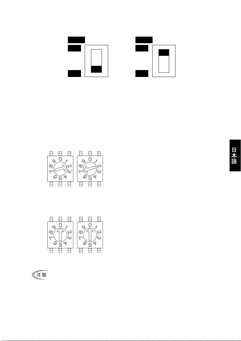
2.3 終端抵抗スイッチ(SW3)
PROFIBUS-DP ネットワークの両端には終端抵抗が必要です。通信カードが PROFIBUS-DP ネットワークのどちらか
一端に取り付けられる場合は,このスイッチを ON することで内蔵の終端抵抗が接続されます。
SW3
ON
SW3
ON
OFF
終端抵抗なし(スイッチ OFF)
図 2.3 終端抵抗 ON/OFF スイッチの設定
OFF
終端抵抗あり(スイッチ ON)
2.4 アドレススイッチ(SW1,SW2)
PROFIBUS-DP 通信上のノードアドレス(局番)を設定するロータリスイッチです。10 進数で 0~99 まで設定可能
です。通信カ-ド上の SW1 が十の位,SW2 が一の位の設定を行います。
なお,ノードアドレスはインバータ機能コード o31 でも設定可能です(10 進数で 0~125 まで設定可能)。o31
で指定したノードアドレス設定を有効にするためには,アドレススイッチを"00"とする必要があります。
例1:ノードアドレス 27 を設定する場合(アドレススイッチで設定)
SW1 SW2
図 2.4 アドレススイッチの設定例1
例2:ノードアドレス 125 を設定する場合(インバータ機能コード o31 で設定)
SW1 SW2
1. インバータの電源 OFF 状態で,
SW1 の設定を"2"にします。
SW2 の設定を"7"にします。
2. インバータの電源を ON すると,アドレス設定完了です。
1. インバータの電源 OFF 状態で,
アドレススイッチの設定を,"00"にします。
2. インバータの電源を ON し,o31 に"125"を設定します。
3. 電源を再投入すると,アドレス設定完了です。
日
本
語
図 2.5 アドレススイッチの設定例2
1. アドレススイッチの設定はインバータの電源を OFF した状態で実施してください。電源 ON 中に
設定を変更した場合は,電源の再投入が必要です。
2. o31 によるノードアドレス設定後は,設定を反映するためにインバータの電源を再投入してくだ
さい。
3. o31 に 126 以上を設定すると,エラーとなり,通信カード上の ERR LED が赤点滅し,インバータ
er5
となります。
は
7
Page 11
2.5 通信速度(ボーレート)の設定
PROFIBUS-DP マスタの通信速度を設定することで,通信カードの通信速度も自動的に設定されます。インバータ
側での設定は必要ありません。
通信カードがサポートする通信速度(ボーレート)は以下のとおりです。
9.6, 19.2, 45.45, 93.75, 187.5, 500 Kbit/s,
1.5, 3, 6, 12 Mbit/s
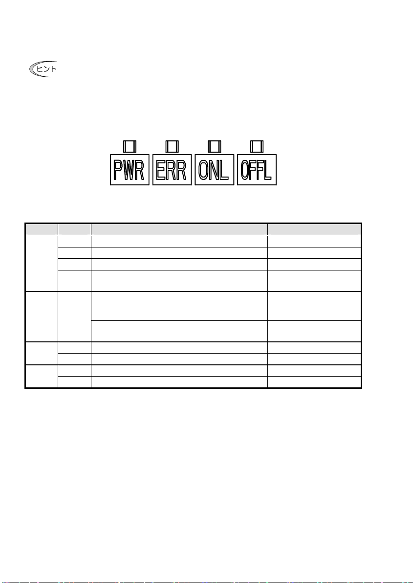
2.6 LED インジケータ
通信カードの状態を示します。LED インジケータには,次の4種類があります。
図 2.6 LED の種類
表 2.3 LED の状態
名称 LED 状態 内容 備考
PWR
緑点滅 電源投入時の自己診断および初期化中 約 0.5s 間実施
赤点滅 PROFIBUS 通信異常 インバータに
ERR 赤点滅 PROFIBUS 設定エラー
ONL 緑 オンライン状態(正常に PROFIBUS 通信している状態)
消灯 オンライン状態でない
OFFL 赤 オフライン状態(PROFIBUS に接続していない状態)
消灯 オフライン状態でない
*1
*2 PPO タイプは PROFIBUS-DP のマスタ設定と通信カードで一致させる必要があります。通信カードの PPO タイ
緑 正常通信中 ―
発生
発生
発生
*
*
er5
赤 ハードウェア異常
(オプション取付け不良またはオプション故障)
インバータ機能コード o30 で設定する PPO タイプと
マスタの PPO タイプが一致していない。 *2
PROFIBUS 設定エラー
ノードアドレスに 126 以上の値が設定されている。
er5
を無視するように設定することも可能です。第 9 章「PROFIBUS 通信異常検出時の動作選択」を参照し
てください。
プはインバータ機能コード o30 で設定します。マスタ側の設定はマスタ用の設定ソフトウェア等で実施しま
す。
インバータに
インバータに
er4
er5
1
1
マスタ側の PPO 設定についてはマスタのマニュアル等を参照してください。
PPO タイプについての詳細は,第 8 章「PROFIBUS プロファイルの詳細説明」を,機能コード o30 につ
いての詳細は第 5 章「インバータ機能コードの設定」を参照してください。
8
Page 12
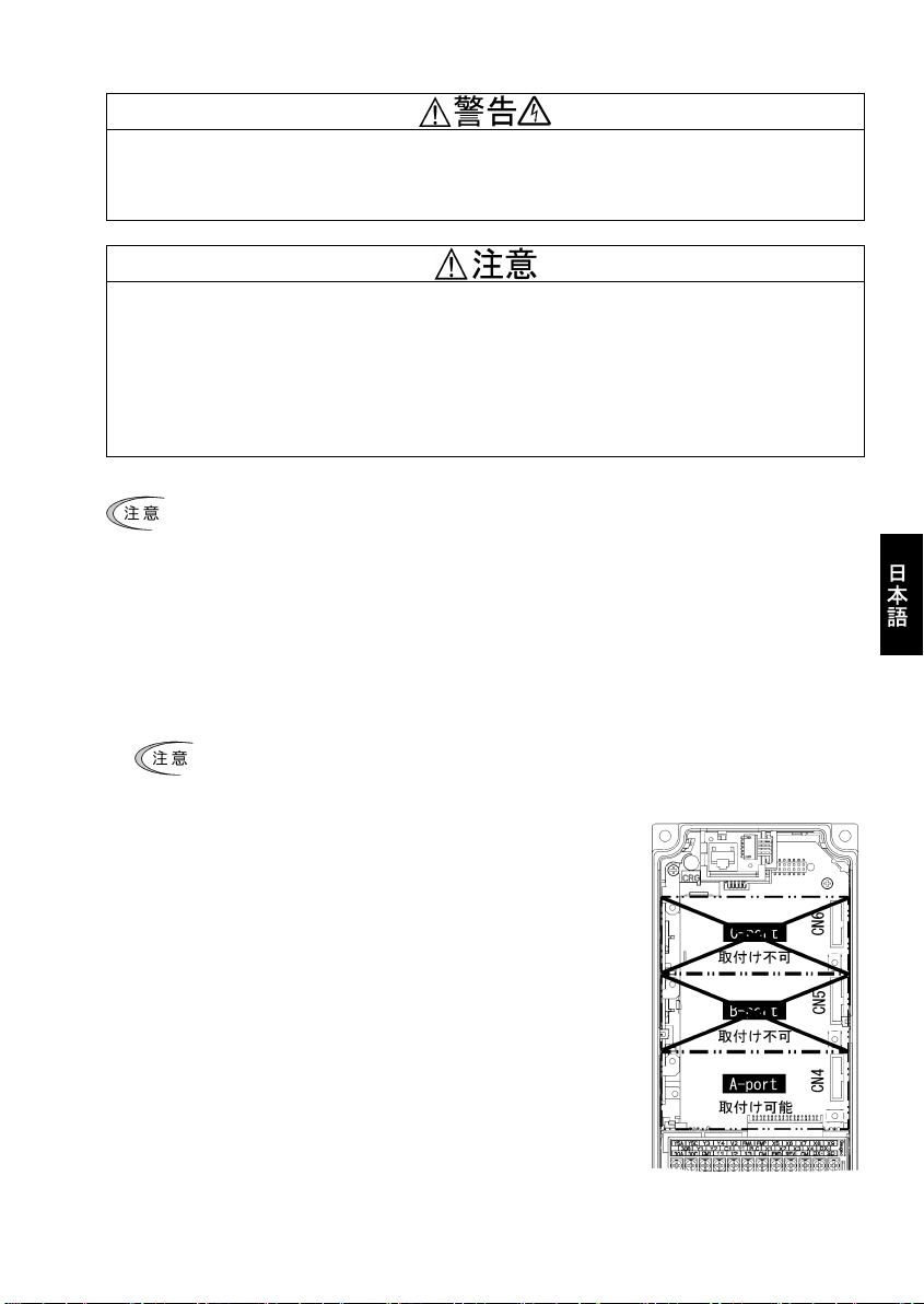
第 3 章 PROFIBUS-DP 通信カードの取付けと取外し
インバータの電源を遮断して 22kW 以下は 5 分以上,30kW 以上は 10 分以上経過してから行ってください。更に LED
モニタおよびチャージランプの消灯を確認し,テスターなどを使用して主回路端子 P(+)-N(-)間の直流中間回路電圧
が安全な値(DC+25V 以下)に下がっていることを確認してから行ってください。
感電のおそれあり
・ 外部あるいは内部部品が損傷・脱落している製品を使用しないでください。
火災,事故,けがのおそれあり
・ 糸くず,紙,木くず,ほこり,金属くずなどの異物がインバータや通信カード内に侵入するのを防止してくださ
い。
火災,事故のおそれあり
・ 製品の取付け,取外し時に不適切な作業を行うと,製品が破損するおそれがあります。
故障のおそれあり
インバータ本体の主回路端子および制御回路端子の配線は,通信カードを取り付ける前に行ってくだ
さい。
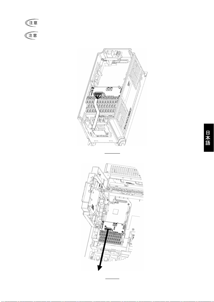
3.1 通信カードの取付け
(1) インバータ本体の表面カバーを取り外し,制御プリント基板を露出してください。通信カードは,インバー
タ本体のオプション接続ポート 3 箇所(A,B,C-port)のうち,A-port にのみ取付け可能です。(図 3.1)
FRENIC-MEGA 取扱説明書の「2.3 配線」を参照してカバーを取り外してください。(30kW 以上はタッチ
パネルケースも開けてください。)
(2) 通信カードの裏面(図 1.1)の CN1 を,インバータ本体の制御プリント基板の A-port(CN4)へ差し込み,付
属ねじで固定してください。(図 3.3)
通信カードの取付け位置決め部(図 1.1)がツメ(図 3.2 の①)にセットされ,CN1(図 3.2 の②)
が確実に差し込まれていることを確認してください。図 3.3 は取付け完了を示します。
日
本
語
(3) 通信カードの配線を行います。
第 4 章「配線」を参照してください。
(4) インバータ本体の表面カバーを元に戻してください。
FRENIC-MEGA 取扱説明書の「2.3 配線」を参照してカバーを取り付
けてください。(30kW 以上はタッチパネルケースも閉じてくださ
い。)
9
図 3.1 0.4kW の例
Page 13
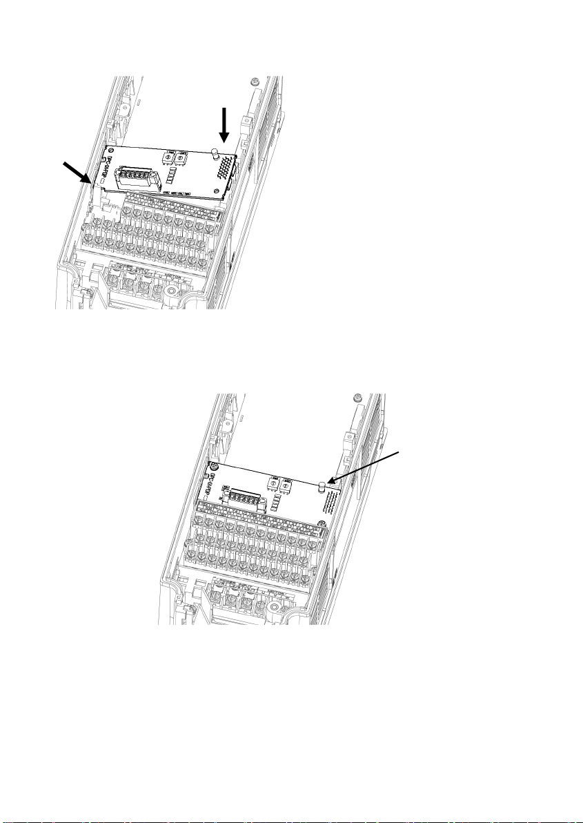
②
①
① カードをツメに引っ掛けるようにしな
がらインバータ本体へ位置決めする。
② コネクタをインバータ本体へ挿入する。
注: 先にコネクタ側を挿入した場合,挿入が不
十分で接触不良となる可能性があります。
図 3.2 カードの取付け
(取外し用つまみ)
図 3.3 取付け完了
3.2 通信カードの取外し
通信カードを取り外す際は,ねじを2ヶ所外し,取外し用つまみ(上図を参照)を引っぱって取り外してくださ
い。
10
Page 14
第 4 章 配線
・ インバータの電源を遮断して 22kW 以下は 5 分以上,30kW 以上は 10 分以上経過してから行ってください。
更に LED モニタおよびチャージランプの消灯を確認し,テスターなどを使用して主回路端子 P(+)-N(-)間
の直流中間回路電圧が安全な値(DC+25V 以下)に下がっていることを確認してから行ってください。
・ 配線作業は,資格のある専門家が行ってください。
感電のおそれあり
・ 一般的に制御信号線の被覆は強化絶縁されていませんので,主回路活電部に制御信号線が直接触れると,
何らかの原因で絶縁被覆が破壊されることがあります。この場合,制御信号線に主回路の高電圧が印加さ
れる危険性がありますので,主回路活電部に制御信号線が触れないように注意してください。
事故のおそれあり,火災のおそれあり
・ インバータ,モータ,配線からノイズが発生します。周辺のセンサーや機器の誤動作に注意してください。
事故のおそれあり
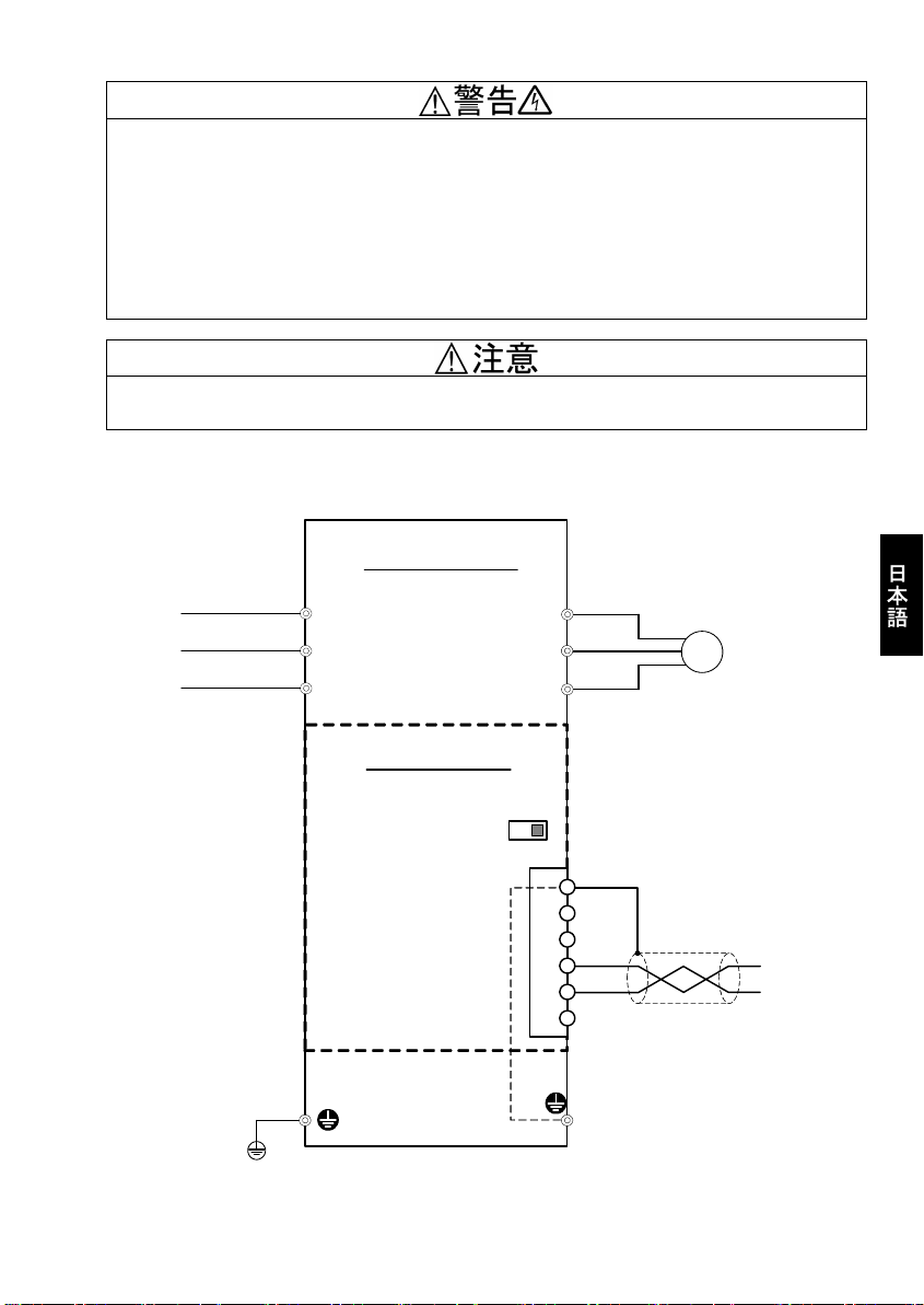
4.1 基本接続図
FRENIC-MEGA
L1/R U
L2/S
L3/T
V
W
モータ
M
OPC-G1-PDP
終端抵抗スイッチ
(SW3)
PROFIBUSコネクタ
(TERM1)
(*)
G
(*) 通信カードをインバータに取り付けることで,この部分が接続されます。
Shield
GND
+5V
A-Line
B-Line
RTS
G
PROFIBUSケーブル
日
本
語
図 4.1 基本接続図
11
Page 15
4.2 PROFIBUS 端子台の配線
基本接続図(図 4.1)および配線例(図 4.3)を参考に,以下の注意事項を守って通信カードへの配線を行って
ください。
(1) 電源を OFF(開)してください。
(2) 通信ケーブルは必ず PROFIBUS 仕様に準拠したシールド付きツイストペアケーブルを使用してください。
推奨ケーブルは,シーメンス製 PROFIBUS FC 標準ケーブル 形式 6XV1 830-0EH10 です。
PROFIBUS の配線全般に関する詳細は PROFIBUS 協会発行の「PROFIBUS-DP ケーブルと機器設置の解説」
(3) PROFIBUS 端子台コネクタ(TERM1)への配線
PROFIBUS ケーブルの電線の被覆をむいて接続してください。電線の被覆むきサイズは図 4.2 に従ってくださ
端子台の推奨締め付けトルクと推奨電線サイズを表 4.1 に示します。
および「PROFIBUS 配線作業ガイド」を参照してください。PROFIBUS 協会の Web サイトから無料でダウ
ンロード可能です。
URL: http://www.profibus.jp/tech/downld.htm
い。シールド線は撚って接続してください。
電線
約 6.0mm
図 4.2 PROFIBUS ケーブル電線の推奨被覆むきサイズ
表 4.1 PROFIBUS 端子台の推奨締め付けトルクと電線サイズ
ねじサイズ 締め付けトルク 電線サイズ
M2 0.22~0.25 N・m AWG28~16 (0.14~1.5mm2 )
PROFIBUS ケーブルは,ノイズによる誤動作を防止するため,インバータ本体の主回路配線,モー
タ配線,その他の動力線とは可能な限り離し,同一ダクト内に入れないでください。また,シール
ド線は必ず接続してください。
(4) インバータの電源投入前に配線を完了してください。
・ 制御回路端子への配線は,主回路の配線とは可能な限り離して配線してください。ノイズによる誤
動作の要因となります。
・ インバータ内部の制御回路配線は,主回路活電部(例えば主回路端子台部)に直接接触しないよう
に内部で束線固定などの処理を行ってください。
線種,配線本数によっては,インバータの表面カバーが浮き上がり,タッチパネルが正しく動作しな
い場合があります。その際は,線種・線径等の変更が必要です。
12
Page 16
4.3 インバータへの配線
PROFIBUS 配線は,主回路の配線とは可能な限り離して配線してください。ノイズによる誤動作の要因
となります。
通信カードからの配線は,インバータ本体の制御端子台上部と表面カバーの間を通してください。
・22kW 以下の場合
・30kW 以上の場合
0.4kW の例
日
本
語
75kW の例
図 4.3 配線例
13
Page 17
第 5 章 インバータ機能コードの設定
通信カードと PROFIBUS-DP マスタ間の通信を行うためには,下記の表 5.1 に示すインバータの機能コードの設定
が必要です。
また,関連するインバータ機能コードを表 5.2 に示します。必要に応じて設定してください。
インバータ機能コードの詳細につきましては,FRENIC-MEGA 取扱説明書の第5 章「機能コード」および RS-485
通信ユーザーズマニュアルの第 5 章「機能コードとデータフォーマット」を参照してください。
表 5.1 PROFIBUS 通信を行うために必要なインバータ機能コード設定
機能コード 説明 工場出荷値 設定変更値 備考
o30 *1 PPO タイプ(データフォー
y98 *2 運転・周波数指令元の選択 0 下記から選択
*1
o30 を設定後は, インバータに設定を反映させるために, インバータの電源を再投入してください。o30 の
マット)の選択
設定内容についての詳細は,第 8 章「PROFIBUS プロファイルの詳細説明」を参照してください。
*2
運転・周波数指令元の選択を設定するインバータ機能コードは,y98 の他にもあります。それらの設定によ
り,より細やかに運転・周波数指令元の選択が可能となります。詳細につきましては,FRENIC-MEGA 取扱説
明書の第 5 章「機能コード」の H30,y98 の項を参照してください。
機能コード 説明 工場出荷値 設定範囲 備考
o27 *1 PROFIBUS 通信異常検出時の動作選択 0 0~15
o28 *1 PROFIBUS 通信異常検出時の動作タイ
o31 *2 ノードアドレス設定 0 0~255
o40~o43 *3 定周期で書込みを行う機能コードの
o48~o51 *3 定周期で読出しを行う機能コードの
W90 PROFIBUS オプション
1
*
o27,o28 についての詳細は,第 9 章「PROFIBUS 通信異常検出時の動作選択」を参照してください。
2
*
o31 についての詳細は,第 2 章「2.4 アドレススイッチ」を参照してください。
3
*
o40~o43 および o48~o51 の詳細は,第 8 章「8.2 (4) PCD1~PCD4」を参照してください。
マー
割付け
割付け
ソフトバージョン
o40~o43 および o48~o51 の設定後は, インバータに設定を反映させるために,インバータの電源を
再投入してください。
0 下記から選択
0,1,6~255 : PPO タイプ1
2,5 : PPO タイプ2
3 : PPO タイプ3
4 : PPO タイプ4
y98 周波数指令元 運転指令元
0 インバータ インバータ
1 PROFIBUS インバータ
2 インバータ PROFIBUS
3 PROFIBUS PROFIBUS
表 5.2 その他関連機能コード
0.0s 0.0s~60.0s
(有効範囲 0~125)
0000
(割付なし)
0000
(割付なし)
オプション
による
0000~FFFF(hex)
0000~FFFF(hex)
-(モニタ専用) 4桁の 10 進数
マスタ側の設定と必
ず一致させてくださ
い
特に問題がなければ
y98=3 を推奨します。
アドレススイッチが"00"の
時に有効。126 以上を設定時
は,ERR LED 点滅および
発生
PPO Type2 または Type4 の時
に有効
V1.23 の場合,"123"と表示
er5
14
Page 18

第 6 章 PROFIBUS 通信接続までの手順説明
本章では, PROFIBUS-DP マスタとインバータを PROFIBUS 通信接続するまでの手順について説明します。
手順は以下の 1~3 です。
1. PROFIBUS-DP マスタ側の設定
2. 通信カードの設定およびインバータ機能コード設定
3. インバータの電源再投入 ⇒ PROFIBUS-DP データの送受信開始
以降,上記の手順 1~3 について説明します。
1. PROFIBUS-DP マスタ側の設定
- マスタ側のノードアドレス,通信速度(ボーレート)を設定します。
- 通信カード用の GSD ファイルを使用し,通信カードをマスタに登録します。
- マスタに登録した通信カードに適用する PPO Type(データフォーマット)を Type1~4 の中から1つ選択
します。
PROFIBUS-DP マスタについての設定方法詳細については,ご使用のマスタのユーザーズマニュアル等を
参照してください。
PPO Type の詳細については,第 8 章「PROFIBUS プロファイルの詳細説明」を参照してください。
本通信カードには GSD ファイルは付属していません。
GSD ファイルは次の Web サイトにてダウンロードください。(会員登録が必要(無料))
富士電機システムズ 技術情報ページ
URL : https://web1.fujielectric.co.jp/Kiki-Info/User/guestlogin.asp
2. 通信カードの設定およびインバータ機能コード設定
- ノードアドレスを設定します。マスタに登録した通信カードのアドレスと必ず一致させてください
- 必要に応じて, インバータ機能コード o27,o28 の設定を行ってください。
- インバータ機能コード o30 で PPO Type を Type1~4 の中から1つ選択します。
必ずマスタで設定した PPOType と一致させてください。また,o30 変更後は, 必ずインバータの電源を再
投入してください。
ノードアドレスの設定方法については,第 2 章「各部の機能・設定」を参照してください。
o27,o28 についての詳細は,第 9 章「PROFIBUS 通信異常検出時の動作選択」を参照してください。
3. インバータの電源再投入 ⇒ PROFIBUS-DP データの送受信開始
o30 の設定後, インバータの電源を再投入した段階で,PROFIBUS-DP マスタ側と通信カードの設定が正しく,
かつ, 適正に配線されていれば,自動的に PROFIBUS-DP の通信が確立し, データの送受信が行われます。
この状態で通信カードの LED 状態は PWR LED 緑点灯, ONL LED 緑点灯となっています。マスタから通信カー
ドに対し, 周波数指令および運転指令等を送信してください。
具体的なデータフォーマットやデータのやりとりについては,第 7 章「インバータを運転する簡単手
順」および第 8 章「PROFIBUS プロファイルの詳細説明」を参照してください。
配線方法については,第 4 章「配線」を参照してください。
。
日
本
語
15
Page 19

第 7 章 インバータを運転する簡単手順
本章では, PROFIBUS-DP マスタからインバータを運転するための最もシンプルなフォーマット(PPO Type3)を
使用した例について, 手順に従って簡単に説明します。PPO Type3 は PROFIBUS からの周波数指令と運転指令に
特化したシンプルなフォーマットです。
他の PPO Type でもフォーマットの割付領域が異なるだけで, 内容的には共通です。
本章は説明の簡単化のためインバータを運転することのみに特化した説明を行っています。更に詳細な説
明については,第 8 章「PROFIBUS プロファイルの詳細説明」を参照してください。
7.1 事前の設定
(1) PROFIBUS-DP マスタ側の設定で通信カードの PPO Type を Type3 にしてください。
PROFIBUS-DP マスタ側での PPO Type の設定方法については, お使いのマスタのユーザーズマニュアル等を
参照してください。
(2) インバータの機能コードを以下の通りに設定します。
F03=60(最高周波数(Hz)),y98=3(PROFIBUS から周波数指令・運転指令有効),o30=3(PPO Type3)
また,必要に応じて o27,o28 の設定をしてください。
設定後,インバータの電源を再起動してください。
o27,o28 についての詳細は,第 9 章「PROFIBUS 通信異常検出時の動作選択」を参照してください。
7.2 運転時の実際のデータやりとり例
説明の前に PPO Type3 のデータフォーマットを以下に示します。以降の説明はこのフォーマットに基づき行いま
す。
要求
(マスタ→スレーブ)
CTW : コントロールワード(2byte)。運転指令を行います。(最下位 bit が運転指令 ON/OFF)
MRV : 周波数指令を行います。最高周波数 F03(Hz)を 4000hex とした時の割合を指定
応答
(スレーブ→マスタ)
STW : ステータスワード(2byte)。インバータの運転状態をモニタします。
MAV : 出力周波数モニタ。最高周波数 F03(Hz)を 4000hex とした時の割合を出力
以降,インバータを 60Hz で正転運転するまでの例を説明します。
(1) インバータの電源を ON すると PROFIBUS-DP 通信が始まります。電源 ON 直後のデータの状態は下記の様にな
っています。
要求
(マスタ→スレーブ)
応答
(スレーブ→マスタ)
STW : 02=PROFIBUS から周波数・運転指令有効, 40=運転指令 ON 準備未完了
MAV : 出力周波数 0Hz
0 1 2 3 (Byte)
CTW MRV
0 1 2 3 (Byte)
STW MAV
0 1 2 3 (Byte)
00 00 00 00
(CTW) (MRV)
0 1 2 3 (Byte)
02 40 00 00
(STW) (MAV)
16
Page 20
(2) 最初の状態では,運転指令 ON の準備ができていない状態(STW=運転指令 ON 準備未完了)になっています。
まず, 運転指令 ON の準備を完了する要求"04 7E"を CTW に入力します。 また, 下の例では同時に周波数指
令 60Hz(=4000h)を MRV に入力しています。
要求
(マスタ→スレーブ)
0 1 2 3 (Byte)
04 7E 40 00
(CTW) (MRV)
CTW : 04=本フレーム内容イネーブル, 7E=運転指令 ON 準備完了要求
MRV : 周波数指令 4000h(周波数指令=F03(Hz))
上記の要求を受け, 通信カードは次の応答をします。
応答
(スレーブ→マスタ)
0 1 2 3 (Byte)
02 31 00 00
(STW) (MAV)
STW : 02=PROFIBUS から周波数・運転指令有効, 31=運転指令 ON 準備完了
MAV : 出力周波数 0Hz
(3) スレーブが運転指令 ON 準備完了になったので CTW に運転指令 CTW="04 7F"を入力してください。
要求
(マスタ→スレーブ)
0 1 2 3 (Byte)
04 7F 40 00
(CTW) (MRV)
CTW : 04=本フレーム内容イネーブル, 7F=運転指令 ON
MRV : 周波数指令 4000h(周波数指令=F03(Hz))
上記の要求を受け, インバータが運転を始めます。通信カードの応答は下記のとおりです。
応答
(スレーブ→マスタ)
0 1 2 3 (Byte)
02 37 ** **
(STW) (MAV)
STW : 02=PROFIBUS から周波数・運転指令有効, 37=運転状態
MAV : 出力周波数加速中
(4) 運転を停止する場合は, CTW="04 7F"→"04 7E"としてください。
要求
(マスタ→スレーブ)
0 1 2 3 (Byte)
04 7E 40 00
(CTW) (MRV)
CTW : 04=本フレーム内容イネーブル, 7E=運転指令 OFF
MRV : 周波数指令 4000h(周波数指令=F03(Hz))
上記の要求を受け, インバータが減速, 停止します。通信カードの応答は下記のとおりです。
応答
(スレーブ→マスタ)
0 1 2 3 (Byte)
02 33/31 ** **
(STW) (MAV)
STW : 02=PROFIBUS から周波数・運転指令有効, 33=減速中/31=運転指令 ON 準備完了(停止時)
MAV : 出力周波数減速中
日
本
語
17
Page 21

(5) 再び運転する場合は, CTW="04 7F"を入力します。ここで, もしも逆転させる場合は, CTW="0C 7F"とします。
下の例では, 逆転指令で, 周波数に 2000h(=30Hz)を設定しています。
要求
(マスタ→スレーブ)
0 1 2 3 (Byte)
0C 7F 20 00
(CTW) (MRV)
CTW : 0C=本フレーム内容イネーブル&逆転, 7F=運転指令 ON
MRV : 周波数指令 2000h(周波数 Hz=F03×2000h/4000h)
上記の要求を受け, インバータが逆転で運転開始します。下の例は, 逆転で速度到達したときの応答です。
応答
(スレーブ→マスタ)
0 1 2 3 (Byte)
03 37 E0 00
(STW) (MAV)
STW : 03=PROFIBUS から周波数・運転指令有効&周波数到達, 37=運転状態
MAV : 出力周波数 E000h(2000h の2の補数表記) (周波数 Hz=F03×(-2000h)/4000h)
(6) MRV に負の値を入力することでも逆転は可能です。下の例では 2000h の2の補数である E000h を入力してい
ます。
要求
(マスタ→スレーブ)
0 1 2 3 (Byte)
04 7F E0 00
(CTW) (MRV)
CTW : 04=本フレーム内容イネーブル, 7F=運転指令 ON
MRV : 周波数指令 E000h(-2000h)(周波数 Hz=F03×(-2000h)/4000h)
上記の要求を受け, インバータが逆転で運転開始します。下の例は, 速度到達したときの応答です。
応答
(スレーブ→マスタ)
0 1 2 3 (Byte)
03 37 E0 00
(STW) (MAV)
STW : 03=PROFIBUS から周波数・運転指令有効&周波数到達, 37=運転状態
MAV : 出力周波数 E000h (周波数 Hz=F03×(-2000h)/4000h)
(7) トリップが発生した場合は,トリップ原因解消後 CTW="0480" を入力するとトリップが解除されます。トリ
ップが解除されたら, CTW="0400"としてください。(CTW の byte1 の最上位 bit がトリップ解除ビットです。)
要求
(マスタ→スレーブ)
0 1 2 3 (Byte)
04 80 10 00
(CTW) (MRV)
CTW : 04=本フレーム内容イネーブル, 80=トリップ解除要求
MRV : 周波数指令 1000h(周波数 Hz=F03×1000h/4000h)
トリップ解除すると, 電源 ON 直後の状態に戻ります。再び運転する場合は, 手順(2)に戻ってください。
応答
(スレーブ→マスタ)
0 1 2 3 (Byte)
02 40 00 00
(STW) (MAV)
STW : 02=PROFIBUS から周波数・運転指令有効, 37=運転状態
MAV : 出力周波数 0000h
18
Page 22
第 8 章 PROFIBUS プロファイルの詳細説明
本通信カードは PROFIBUS 協会が規定したモータコントロール用のプロファイルである PROFIdrive V2 をサポー
トしています。本章では,この PROFIdrive プロファイルについて説明します。
8.1 サポートする PPO の説明
PROFIdrive では, PPO(Parameter Process-data Object)と呼ばれるデータフォーマットを複数定義しています。
通信カードがサポートする PPO は図 8.1 に示す 4 種類です。PPO Type の選択はインバータ機能コード o30 で設
定してください(表 8.1)。各 PPO の特徴を表 8.2 に,PPO の各要素についての説明を表 8.3 および表 8.4 に示し
ます。
PCV PCD
CTW
PCA IND PVA
1 2 3 4 5 6 (word)
PPO Type1
1 2 3 4 5 6 7 8 9 10 (word)
PPO Type2
1 2 (word)
PPO Type3
1 2 3 4 5 6 (word)
PPO Type4
図 8.1 サポートする PPO のフォーマット
表 8.1 インバータ機能コード o30 による PPO Type 選択
o30 PPO 備考
0, 1, 6~255 PPO Type1 工場出荷状態での PPO Type
2, 5 PPO Type2
3 PPO Type3
4 PPO Type4
インバータ機能コード o30 を設定後は, インバータに設定を反映させるために, インバータの電源を
再投入してください。
STW
MRV
PCD1 PCD2 PCD3 PCD4
MAV
日
本
語
19
Page 23
表 8.2 各 PPO Type の特徴
PPO 特徴
PPO Type1 標準的なフォーマット。運転指令/運転状態モニタと周波数指令/出力周波数モニタに
加えて, インバータ機能コードの単発的なアクセスが可能です。
PPO Type2 全ての機能を網羅したフォーマット。運転指令/状態モニタ, 周波数指令モニタ, イン
バータ機能コードの単発アクセス, 事前に割付した 4 種類のインバータ機能コードの
定周期アクセスが可能です。
PPO Type3 運転指令/状態モニタと周波数指令/モニタに特化したシンプルなフォーマットです。
PPO Type4 運転指令/状態モニタ, 周波数指令/モニタと事前に割付した 4 種類のインバータ機能
コードの定周期アクセスが可能なフォーマットです。
表 8.3 PPO 内の各要素の説明
要素 説明
PCD
PCV
要素 説明
PCD CTW/STW 要求 CTW: コントロールワード。マスタから運転指令を行います。
応答 STW: ステータスワード。インバータの運転状態応答です。
MRV/MAV 要求 MRV: 設定周波数。最高周波数 F03 を 4000(Hex)とする割合で指定。
応答 MAV: 出力周波数。最高周波数 F03 を 4000(Hex)とする割合で応答。
PCD1 要求 o40 で割付したインバータ機能コードを書込みします。
応答 o48 で割付したインバータ機能コードを常時モニタします。
PCD2 要求 o41 で割付したインバータ機能コードを書込みします。
応答 o49 で割付したインバータ機能コードを常時モニタします。
PCD3 要求 o42 で割付したインバータ機能コードを書込みします。
応答 o50 で割付したインバータ機能コードを常時モニタします。
PCD4 要求 o43 で割付したインバータ機能コードを書込みします。
応答 o51 で割付したインバータ機能コードを常時モニタします。
PCV PCA 要求
応答 指定されたパラメータとアクセス結果を応答します。
IND 要求・応答
PVA 要求・応答 パラメータの書込み値/読出し値を表示します。
o40~o43,o48~o51 についての詳細は,本章の「8.2 (4) PCD1~PCD4」を参照してください。
PROFIBUS-DP マスタと常時データ通信を行う領域です。運転指令/運転状態モニタ, 周波数
指令/出力周波数モニタが該当します。また, PPO Type2 および Type4 では, 任意のインバ
ータ機能コードを割付けて, 常時書込み/モニタする機能もサポートしています。(書込み,
読出しでそれぞれ 4 種類まで)
パラメータ(インバータ機能コード, PROFIdrive 固有パラメータ)への単発的なアクセス
を行う領域です。この領域は PPO Type1 および Type2 がサポートしています。
表 8.4 PCV 部と PCD 部の各要素の説明
パラメータ(インバータ機能コードおよび PROFIBUS パラメータ)
要求は PROFIBUS-DP マスタから通信カードへのデータ送信を, 応答は通信カードから PROFIBUS-DP
マスタへのデータ送信を意味します。
の指定と, そのパラメータに対してアクセス方法(読出し/書込み
等)の指定をします。
配列型パラメータのインデックス指定に使用します。また, イン
バータ機能コードの番号指定に使用します。
20
Page 24
8.2 PCD の説明
PCD は PROFUBUS-DP マスタと通信カード間で常時データをやり取りする領域です。運転指令/運転状態モニタ, 周
波数指令/周波数モニタおよび, 事前に割付けた 4 種類のインバータ機能コードに対する常時アクセスを行う
PCD1~4 の領域からなります。
(1) CTW(コントロールワード)
PROFIBUS-DP マスタからインバータに運転指令等を行うワード領域です。
15 14 13 12 11 10 9 8 7 6 5 4 3 2 1 0 (bit)
0 0 0 0
運転
方向
PCD
有効
00
ALM
RST設定有効
Ramp
Ramp有効運転可能ON3/
非固定
OFF3
ON2/
OFF2
ON/
OFF
表 8.5 CTW のビット説明
bit False (0) True (1)
0 ON/OFF 運転指令 OFF 運転指令 ON
1 ON2/OFF2 フリーラン停止指令(OFF2) 運転指令 ON 準備完了要求その1(ON2)
2 ON3/OFF3 機能コード H56 の減速時間による停止指令
運転指令 ON 準備完了要求その2(ON3)
(OFF3)
3 運転可能 インバータ運転無効 インバータ運転可能
4 Ramp 有効 出力周波数 0 固定 ランプジェネレータ(加減速器)有効指令
5 Ramp
非固定
ランプジェネレータ(加減速器)フリーズ。
出力周波数はその時点の値で固定
加減速フリーズ状態解除指令
6 設定有効 停止 ON ビット有効
7 ALM RST アラームリセットしない
アラームリセット(リセット後, 運転指令
ON 準備未完了の状態になります)
10 PCD 有効 PCD 部(CTW+MRV)の入力無効 PCD 部(CTW+MRV)の入力有効
11 運転方向 正転方向 逆転方向
通常の使用状況においては, bit1~6 および bit10 は常時1で問題ないと思われます。
PROFIdrive プロファイルは状態遷移させて制御を行います。従って単に運転指令を ON してもインバ
ータは運転しません。 インバータを運転させるためには PROFIdrive プロファイルの状態遷移条件に
従い, しかるべき状態になった上で運転指令を ON する必要があります。状態は次項で説明する STW
(ステータスワード)で判断可能です。
PROFIdrive の状態遷移条件については, 次項「(2) STW(ステータスワード)」および図 8.2 を参照し
てください。
状態遷移による厳密な制御は特に必要ないという方は,第 7 章「インバータを運転する簡単手順」で
説明している内容に従って頂いて問題ありません。
日
本
語
21
Page 25

(2) STW(ステータスワード)
インバータの運転状態等をモニタするワード領域です。
STW は PROFIdrive の状態遷移を表します。状態遷移については,図 8.2 を参照してください。
15 14 13 12 11 10 9 8 7 6 5 4 3 2 1 0 (bit)
0 0 0 0 0 FDT R/L FAR 0
表 8.6 STW のビット説明
bit False (0) True (1)
0 ON 準備完 運転指令 ON 準備未完了状態 運転指令 ON 準備完了状態
1 運転準備完 運転準備未完了状態 運転準備完了状態
2 運転状態 運転不能状態 運転中
3 ALM インバータトリップなし インバータトリップ中
4 ON2/OFF2 CTW の ON2 ビット=0 (OFF2) CTW の ON2 ビット=1 (ON2)
5 ON3/OFF3 CTW の ON3 ビット=0 (OFF3) CTW の ON3 ビット=1 (ON3)
6 ON 禁止 運転指令 ON 準備完了状態
(bit0 を論理反転したもの)
8 FAR 設定周波数に未到達 設定周波数に到達
9 R/L PROFIBUS からの周波数指令・運転指
令が共に無効
10 FDT 出力周波数が, インバータ機能コー
ド E31 で設定した周波数未満である。
ON禁止ON3/
ON2/
OFF3
OFF2
運転指令 ON 準備未完了状態
(bit をの論理反転したもの)
PROFIBUS-DP からの周波数指令・運転指令
いずれかが有効
出力周波数が, インバータ機能コード
E31 で設定した周波数以上である。
ALM
運転状態運転
準備完
準備完
ON
22
Page 26

以下に PROFIdrive の状態遷移図を示します(図 8.2)。
インバータの電源 ON 直後は「S1:運転指令 ON 準備未」から始まり, 順次 CTW の bit 操作を行うことで, 「S2:
運転指令 ON 準備完」→「S3:運転準備完」へ遷移し, 「S4:運転状態」に遷移した状態で, インバータ運転
状態となります。S4 の状態から, 運転指令を OFF すると「S5:運転指令 OFF」に遷移し, モータ停止後 S2 あ
るいは S1 に遷移します。
図8.2では, 説明の簡単化のため CTW の bit4~6 および bit10 は常時1としています。これらの
bit 値が1でないと状態遷移が正しくても, インバータは運転状態となりません。
インバータ電源ON
アラームリセット
→(CTW: bit7=0 1)
STW:xxxx xxxx xxxx 1000
モータ停止検出
or
運転可能=0
(CTW: xxxx x1xx x111 0110)
)OFF2(フリーラン指令
任意の状態で
トリップ発生
トリップ中
モータ停止検出
(CTW: xxxx x1xx x111 001x)
(CTW: xxxx x1xx x111 110x)
(CTW: xxxx x1xx x111 1100)
or
運転可能=0
or
)OFF2(フリーラン指令
)OFF2(フリーラン指令
STW:xxxx xxxx x1xx x000
OFF and ON2 and ON3
(CTW: xxxx x1xx x111 x110)
STW:xxxx xxxx x0xx x001
ON
(CTW: xxxx x1xx x111 x111)
STW:xxxx xxxx x0xx x011
運転可能=1
( CTW: xxxx x1xx x111 1111)
:S1 運転指令ON
準備未
S2:運転指令ON
準備完
S3:運転準備完
OFF2 or OFF3
(CTW: bit2=0 or bit3=0)
OFF
(CTW: xxxx x1xx x111 x110)
(CTW: xxxx x1xx x111 0111)
運転可能=0
OFF2 or OFF3
(CTW: bit2=0 or bit3=0)
(CTW: xxxx x1xx x111 1101)
日
本
語
(CTW: xxxx x1xx x111 1110)
OFF3
(CTW: xxxx x1xx x111 1011)
インバータ機能コード S06/S01,S05,S19 による運転指令および周波数/速度指令について
S06 による運転指令(bit0,1)および S01,S05,S19 による周波数・速度指令は,状態 S1 の時に可能
です。これらの指令を行っている時に状態 S1 以外に遷移させた場合は,即時 CTW および MRV による指
令に従います。なお,S06 の bit2~15 は,どの状態でも使用可能です。
状態 S4 または状態 S5 で OFF2(フリーラン停止)または OFF3(急減速停止)によって状態 S1 に遷移させ
た場合,状態 S1 であってもインバータ機能コード S06 による運転指令は無効(正確には,0Hz で運転
状態)となります。この場合,ON2 あるいは ON3 を入力することで,S06 による運転指令を有効にする
ことができます。
:S4 運転状態
STW:xxxx xxxx x0xx x111
OFF
OFF3
(CTW: xxxx x1xx x111 1010)
ON
(CTW: xxxx x1xx x111 1111)
:S5 運転指令OFF
減速停止中
急減速停止中
STW:xxxx xxxx x0xx x011
図 8.2 PROFIdrive の状態遷移図
23
注意
1. bitの状態を示す記号の意味
0 : False
1 : True
x : Don’t care
2. CTWのbit状態の下線部は, 状態遷移
。 のトリガとなるbitを示す
Page 27

PROFIBUS-DP からオートチューニング(インバータ機能コード P04/A18/b18/r18)を実施した場合は,
状態遷移に関わらず,規定の周波数でインバータが運転します。
オートチューニングについては,FRENIC-MEGA 取扱説明書の第 4 章「4.1.7 機能コードの基本設定・チュ
ーニング<2>」を参照してください。
(3) MRV(設定周波数)/MAV(出力周波数)
周波数を設定/モニタするワード領域です。
MRV: 設定周波数。PROFIBUS-DP マスタからインバータの周波数を設定します。
MAV: 出力周波数。インバータの現在の出力周波数を応答します。
共に, 最高周波数 F03(Hz)を 4000(hex)とした場合の割合で表記しています。換算式は以下の通りです。
MAV or MRV ×=×=
周波数(Hz)
(Hz)機能コードF03
(Hz)機能コードF03周波数(Hz) あるいは 4000(hex)
4000(hex)
MAV or MRV
負の値は2の補数表現となります。逆転時は, MAV(出力周波数)は負の値として出力されます。
MRV(設定周波数)に負の値を設定すると, 正転運転しても, 運転方向は逆転になります。
(4) PCD1~PCD4
PPO Type2 および Type4 のみがサポートしているワード領域で, 事前に割付けしたインバータ機能コードに
対して, 常時書込み/モニタが可能です。書込み/モニタでそれぞれ個別に4種類ずつの機能コードの割付け
が可能です。
割付けしたインバータ機能コードの書込み/モニタされる値は, 機能コードごとにインバータで
規定されたフォーマットに従っています。
インバータ機能コードのそれぞれのフォーマットについては,RS-485 通信ユーザーズマニュアルの
第 5 章「5.2 データフォーマット」を参照してください。
機能コードの割付けは, インバータ機能コード o40~o43 および o48~o51 で行います(表 8.7)。また, o40
~o43 および o48~o51 を使った機能コードの割付方法については, 次ページの表 8.8 に示します。
表 8.7 PCD1~4 に割付けするための機能コード
PCD 領域 機能コード 備考
要求 PCD1 o40 PNU915, index1 でも割付可 *1
(機能コード書込み) PCD2 o41 PNU915, index2 でも割付可 *1
PCD3 o42 PNU915, index3 でも割付可 *1
PCD4 o43 PNU915, index4 でも割付可 *1
応答 PCD1 o48 PNU916, index1 でも割付可 *1
(機能コードモニタ) PCD2 o49 PNU916, index2 でも割付可 *1
PCD3 o50 PNU916, index3 でも割付可 *1
PCD4 o51 PNU916, index4 でも割付可 *1
*1 PNU915, PNU916 とは PROFIdrive 固有パラメータのことです。それらについての詳細は,
本章の「8.3 (4) PROFIdrive 固有パラメータ」を参照してください。
o40~o43およびo48~o51 を使用した機能コードの割付方法については,次ページを参照してください。
24
Page 28

インバータ機能コード o40~o43 および o48~o51 による機能コードの割付けは, 4桁の 16 進数で機能コー
ド種別(表 8.8)と番号を指定することで行います。
□□□□
インバータ機能コード S06 による運転指令(bit0, 1)および S01,S05,S19 による周波数・速度
指令は,状態 S1 の時に可能です。これらの指令を行っている時に状態 S1 以外に遷移させた場合
は,即時 CTW および MRV による指令に従います。なお, S06 の bit2~15 は,どの状態でも使用可
インバータ通信専用機能コード S01, S05, S19 については, RS-485 通信ユーザーズマニュアルの第 5
能です。
章「5.1 通信専用機能コード」を参照してください。
種別 種別コード 機能コード名称 種別 種別コード 機能コード名称
S 2 02h 指令・機能データ r 12 0Ch モータ 4 機能
M 3 03h モニタデータ J 14 0Eh アプリケーション機能 1
F 4 04h 基本機能 y 15 0Fh リンク機能
E 5 05h 端子機能 W 16 10h モニタデータ 2
C 6 06h 制御機能 X 17 11h アラーム 1
P 7 07h モータ 1 機能 Z 18 12h アラーム 2
H 8 08h ハイレベル機能 b 19 13h モータ 3 機能
A 9 09h モータ 2 機能 d 20 14h アプリケーション機能 2
o 10 0Ah オプション機能
例:F26 の場合 F ⇒ 種別コード 04
26 ⇒ 1A(16 進表記)
o40~o43 および o48~o51 の設定後は, インバータに設定を反映させるために,インバータの電源
を再投入してください。
書込みの割付(o40~o43)に同じ機能コードを複数割付した場合, o コードの番号が一番小さいも
のへの割付だけが有効となり, 残りは割付なしと判断します。
異なる機能コード割付けであっても,インバータ機能コード S01,S05,S19(周波数・速度指令)
のうち 2 つ以上を同時割付けした場合, o コードの番号が一番小さいものへの割付だけが有効とな
り,残りは割付なしと判断します。(内部的にはこれら3つの機能コードは同一の扱いとなってい
ます。)
機能コード番号(16進表記)
機能コード種別(表 8.8 による)
表8.8 機能コード種別
"041A"
日
本
語
25
Page 29

8.3 PCV の説明
PCV はパラメータ(インバータ機能コード, PROFIdrive 固有パラメータ)の単発的なアクセスを行う領域です。
この領域は PPO Type1 および Type2 がサポートしています。PCV 部の構成を図 8.3 に示します。
1 2 3 4 (word)
PCV 部 PCA IND
図 8.3 PCV 部の全体構成
PVA
(H) (L)
(1) PCA および IND
2つの領域でパラメータの指定を行います。PCA と IND は更に以下の構成からなります。
15 14 13 12 11 10 9 8 7 6 5 4 3 2 1 0 (bit)
PCA RC SPM PNU
15 14 13 12 11 10 9 8 7 6 5 4 3 2 1 0 (bit)
IND SubIndex 使用しません
RC: 要求コード/応答コード(表 8.9)
SPM: 使用しません。0 固定。
PNU: アクセスするパラメータの番号を指定。
SubIndex: インバータ機能コードの番号(機能コード種別に続く数字)を指定。もしくは,
配列型 PROFIdrive 固有パラメータのインデックス番号を指定。
インバータ機能コードの指定は, PNU 領域と SubIndex 領域を使って行います。PNU 領域には(機
能コード種別(表 8.8)+100h)の値を, SubIndex の領域には機能コード番号を入力します。
インバータ機能コードの指定方法, 読出し/書込み方法については, 本章の「8.3 (3)インバータ機能
コードおよび PROFIdrive 固有パラメータへのアクセス方法」を参照してください。
表 8.9 RC の説明
RC 要求/応答 内容
0 要求 要求無し
1 (マスタ→スレーブ) パラメータ値読出し
2 パラメータ値書込み(word)
3~5 使用しません
6 配列型パラメータの値の読出し
7 配列型パラメータの書込み(配列 word)
8 使用しません
9 配列型パラメータの配列要素数読出し
10~15 使用しません
0 応答 応答なし
1 (スレーブ→マスタ) パラメータ値(word)を正常転送した
2, 3 使用しません
4 パラメータ値(配列 word)を正常転送した
5 使用しません
6 配列要素数の正常応答
7 転送エラー(PVA にエラー番号が格納)*1
8~15 使用しません
*1 エラー番号の内容については,表 8.10 を参照してください。
26
Page 30

表 8.10 パラメータアクセスエラー時のエラー番号一覧
エラ―番号
RC
(PVA に表示)
7 0 存在しないパラメータを指定
1 パラメータ書込み不可
2 パラメータ設定範囲外
3 無効な SubIndex 指定
11 運転中あるいは端子台 ON 中パラメータ書込み不可エラー
17 読出し処理実行不可能
101 リンク優先エラー
104 パラメータ書込み中 busy エラー
(2) PVA
書込み/読出しパラメータ値を示す2ワード領域です。本通信カードでは, PVA の下位 1 ワードのみ(PCV 部
の頭から数えて4ワード目)を使用します。
パラメータの書込みの場合は, マスタから書込み値を入力します。読出しの場合は, 応答時にこの領域に読
出し値が出力されます。パラメータアクセスにエラーがある場合(応答 RC=7 の時)は, 応答時にこの領域に
エラー番号(表 8.10)が出力されます。
15 14 13 12 11 10 9 8 7 6 5 4 3 2 1 0 (bit)
PVA
使用しません
(H)
15 14 13 12 11 10 9 8 7 6 5 4 3 2 1 0 (bit)
PVA
書込み値/読出し値 or エラー番号(表 8.10)
(L)
内容
日
本
語
27
Page 31

(3) インバータ機能コードおよび PROFIdrive 固有パラメータへのアクセス方法
1. PNU 領域と SubIndex 領域で, アクセスするパラメータを指定します(図 8.4 参照)。インバータ機能コ
ードを指定する場合は, PNU に 100(hex)+機能コード種別(表 8.8 参照), Subindex に機能コード番号(機
能コード種別に続く番号。F01 ならば"01"の部分)を指定します。
2. RC 領域で, 指定したパラメータに対してのアクセス方法(書込み, 読出しなど)を指定します。RC の
詳細は表 8.9 を参照してください。
3. パラメータの書込みの場合は, PVA 領域に書込み値を入力します。読出しの場合は, 応答時に指定した
パラメータの値がスレーブから出力されます。アクセス結果がエラーだった場合は, 応答時の RC が 7
となり, PVA 領域に表 8.10 に示すエラー番号が出力されます。
インバータ機能コード S06 による運転指令(bit0,1)および S01,S05,S19 による周波数・速度指
令は,状態 S1 の時に可能です。これらの指令を行っている時に状態 S1 以外に遷移させた場合は,
即時 CTW および MRV による指令に従います。なお,S06 の bit2~15 は,どの状態でも使用可能で
す。
インバータ通信専用機能コード S01,S05,S06,S19 については,RS-485 通信ユーザーズマニュアル
の第 5 章「5.1 通信専用機能コード」を参照してください。
インバータ機能コードごとにそれぞれ規定のフォーマットが定められています。それぞれのフォーマ
ットについては, RS-485 通信ユーザーズマニュアルの第 5 章「5.2 データフォーマット」を参照して
ください。
15 12 10 8 7 0 (bit)
PCA
RC
(表 8.9 による)
0 PNU
インバータ機能コード指定時:
PROFIdrive 固有パラメータ:
指定時
100(hex)+表 8.8 の値
PNU 番号(表 8.11)
15 8 7 0 (bit)
IND SubIndex 使用しない。00(hex)固定
インバータ機能コード指定時: 機能コード番号
PROFIdrive 固有パラメータ:
(配列型)指定時
インデックス番号
(表 8.11)
15 8 7 0 (bit)
PVA
(H)
使用しない。0000(hex)固定
15 8 7 0 (bit)
PVA
(L)
書込み値/読出し値 or エラー番号(表 8.10)
図 8.4 パラメータのアクセス方法
次ページ以降に実際にパラメータにアクセスした例を示します。
28
Page 32

例1. インバータ機能コード F26 に値として 15 を書込みする場合
① マスタから F26 に 15 を書込む要求を送信します。
RC=2(hex) → パラメータ書込み(word)
PNU=104(hex), SubIndex=1A(hex) → F26 を指定(100h+種別 04h=104h, 機能コード番号=1Ah)
PVA=0000 000F(hex) → 書込み値15(=000Fh)を入力
15 8 7 0 (bit)
要求
(マスタ→スレーブ)
IND 1A(hex) (00h 固定)
PVA(H) (0000h 固定)
PVA(L) 000F(hex)
PCA 2(hex) 104(hex)
② 通信カードからの応答例です。(正常応答)
RC=1(hex) → パラメータ値の正常転送
PNU=104(hex), SubIndex=1A(hex) → アクセスしたパラメータは機能コード F26
PVA=0000 000F(hex) → 書込まれた値は15
応答
(スレーブ→マスタ)
IND 1A(hex) (00 固定)
PVA(H) (0000 固定)
PVA(L) 000F(hex)
15 8 7 0 (bit)
PCA 1(hex) 104(hex)
③ 書込みエラーがあった場合の応答例(範囲外エラー時)
RC=7(hex) → パラメータの転送エラー
PNU=104(hex), SubIndex=1A(hex) → アクセスしたパラメータは機能コード F26
PVA=0000 0002(hex) → エラーコード2(パラメータ範囲外エラー)
応答
(スレーブ→マスタ)
IND 1A(hex) (00 固定)
PVA(H) (0000 固定)
PVA(L) 0002(hex)
15 12 11 8 7 0 (bit)
PCA 7(hex) 104(hex)
日
本
語
29
Page 33
例2. インバータ機能コード y98 の値を読出しする場合
① マスタから y98 の読出し要求を送信します。
RC=1(hex) → パラメータ読出し
PNU=10F(hex), SubIndex=62(hex) → y98(100h+種別 0Fh=10Fh, 機能コード番号=62h)を指定
PVA=0000 0000(hex) → PVA には特に何も入力する必要なし
15 8 7 0 (bit)
要求
(マスタ→スレーブ)
IND 62(hex) (00h 固定)
PVA(H) (0000h 固定)
PVA(L) 0000(hex)
PCA 1(hex) 10F(hex)
② 通信カードからの応答例です。(正常応答)
RC=1(hex) → パラメータ値の正常転送
PNU=10F(hex), SubIndex=62(hex) → アクセスしたパラメータは機能コード y98
PVA=0000 0003(hex) → 読出し値 3
応答
(スレーブ→マスタ)
IND 62(hex) (00 固定)
PVA(H) (0000 固定)
PVA(L) 0003(hex)
15 8 7 0 (bit)
PCA 1(hex) 10F(hex)
③ 読出しエラーがあった場合の応答例(機能コードが存在しない)
RC=7(hex) → パラメータの転送エラー
PNU=10F(hex), SubIndex=64(hex) → アクセスしたパラメータはインバータ機能コード y100
PVA=0000 0000(hex) → エラーコード 0(存在しないパラメータを指定)
応答
(スレーブ→マスタ)
IND 64(hex) (00 固定)
PVA(H) (0000 固定)
PVA(L) 0000(hex)
15 8 7 0 (bit)
PCA 7(hex) 10F(hex)
30
Page 34

例3. 配列型の PROFIdrive 固有パラメータ PNU947(アラーム履歴)を読出しする場合
① マスタから PNU947 の読出し要求を送信します。(下記の例はインデックス1を読出し)
RC=6(hex) → 配列型パラメータ読出し
PNU=3B3(hex), SubIndex=1(hex) → PNU947(=3B3h),インデックス 1 を指定
PVA=0000 0000(hex) → PVA には特に何も入力する必要なし
15 8 7 0 (bit)
要求
(マスタ→スレーブ)
IND 01(hex) (00h 固定)
PVA(H) (0000h 固定)
PVA(L) 0000(hex)
PCA 6(hex) 3B3(hex)
② 通信カードからの応答例です。(正常応答)
RC=4(hex) → 配列型パラメータ値の正常転送
PNU=3B3(hex), SubIndex=01(hex) → アクセスしたパラメータ PNU947(=3B3h),インデックス1
PVA=0000 7511(hex) → 読出し値 7511(hex) ; PROFIBUS 通信エラー(
PNU947 の値については,第 10 章「アラームコード一覧」を参照してください。
応答
(スレーブ→マスタ)
IND 01(hex) (00 固定)
PVA(H) (0000 固定)
PVA(L) 7511(hex)
15 8 7 0 (bit)
PCA 4(hex) 3B3(hex)
er5
③ 読出しエラーがあった場合の応答例(配列型読出しで読出ししなかった時)
RC=7(hex) → パラメータの転送エラー
PNU=3B3(hex), SubIndex=01(hex) → アクセスしたパラメータはインバータ機能コード y100
PVA=0000 0003(hex) → エラーコード 3(無効な SubIndex 指定)
応答
(スレーブ→マスタ)
IND 1A(hex) (00 固定)
PVA(H) (0000 固定)
PVA(L) 0003(hex)
15 8 7 0 (bit)
PCA 7(hex) 3B3(hex)
)
日
本
語
31
Page 35

(4) PROFIdrive 固有パラメータ
通信カードでサポートする PROFIdrive 固有パラメータを表 8.11 に示します。Index の欄に記載がある PNU
は, 配列型パラメータであるこということを示します。
表 8.11 PROFIdrive 固有パラメータ一覧
PNU Index 内容 範囲 R/W 備考
915 1~4 PCD1~4(要求)への機能コード割付け
(機能コード書込み)
916 1~4 PCD1~4(応答)への機能コード割付け
(機能コードモニタ)
0000~
FFFF(hex)
0000~
FFFF(hex)
R/W o40~o43 と同一
R/W o48~o51 と同一
918 なし ノードアドレス 0~125 R
927 なし PCV 領域のアクセス権限
0 : 書込禁止
1 : 書込許可
947 1 故障履歴(最新)
9 故障履歴(1回前)
17 故障履歴(2回前)
25 故障履歴(3回前)
上記
0 固定
以外
0, 1 R/W 書込禁止後はこの
PNU のみ書込み可と
なります。
表 10.1 による R PROFIdrive 用のアラ
ームコード(マルフ
ァンクションコー
ド)で表示されます。
機能コード M16~M19
によるアラームコー
ドとは別のフォーマ
ットです。*1
現在のボーレート 963 なし
0 : 不定
2 : 19.2 kbit/s
4 : 93.75 kbit/s
6 : 500 kbit/s
8 : 3Mbit/s
1 : 9.6 kbit/s
3 : 45.45 kbit/s
5 : 187.5 kbit/s
7 : 1.5Mbit/s
9 : 6Mbit/s
0~10 R
10 : 12Mbit/s
965 なし PROFIdrive のバージョン 2 固定 R PROFIdrive V2
を示す。
967 なし 最後に送信した CTW 0000~
R
FFFF(hex)
968 なし 最新の STW 0000~
R
FFFF(hex)
970 なし インバータの初期化
0, 1 R/W H03 と同等機能
(1→0 で初期化実行)
*1 マルファンクションコードおよびアラームコードについては, 第 10 章「アラームコード一覧」を参照
してください。
32
Page 36

第 9 章 PROFIBUS 通信異常検出時の動作選択
PROFIBUS-DP マスタは,通信状態を監視するために,通信タイムアウト検出時間であるウオッチドッグタイマ(以
下,WDT と記載)を設定することができます。通信カードは,いったんデータを受信してから,この WDT で設定
した時間を超えても次のデータ受信がない場合,通信異常と判断します。通信異常と判断した後のインバータの
動作は,インバータ機能コード o27,o28 で設定することが可能です(表 9.1)。
PROFIBUS-DP マスタの WDT の設定については,お使いのマスタのユーザーズマニュアル等を参照してくだ
さい。
通信異常時の通信カードの LED 状態については, 第 2 章「2.6 LED インジケータ」を参照してください。
er5
インバータの電源 ON 直後に通信異常があっても
も受信した後に, 通信異常を検出した場合に
表 9.1 PROFIBUS 通信異常検出時の動作選択
o27 o28 異常検出時の動作 備考
0,
4 ~ 9
1 0.0s~60.0s
2 0.0s~60.0s
3,
13~15
10 -
11 0.0s~60.0s
12 0.0s~60.0s
-
-
er5
を軽故障対象に選択した場合は, 機能コード o27 の設定に関わらず, 通信異常があっても運
転を継続します。
即時フリーラン&
o28 で設定した時間経過後,フリーラン&
o28 で設定した時間内に通信リンクが復帰すれば異常
を無視。タイムアウトならフリーラン&
通信異常を無視して現状維持。
er5
は発生しません。)
(
即時強制減速。停止後
o28 で設定した時間経過後,強制減速し,停止後
o28 で設定した時間内に通信リンクが復帰すれば異常
を無視。タイムアウトなら強制減速後,
er5
トリップ。
er5
。 強制減速の時間はインバ
トリップとなりません。正常データを1回で
er5
トリップとなります。
er5
。
er5
。
通信異常を検出した場
合, LED は通信異常表示
となります。
(PWR 赤点滅, OFFL 赤)
ータ機能コード F08 によ
ります。
er5
。 同上
同上
er5
。
軽故障選択については,FRENIC-MEGA 取扱説明書の第 5 章「機能コード」の H81 を参照してください。
日
本
語
33
Page 37

第 10 章 アラームコード一覧
インバータがトリップした時の要因をアラームコードとして PROFIBUS 通信で確認することができます。
アラームコードは以下の 2 つの方法で確認することができます。
1. PROFIdrive 固有パラメータ PNU947 で確認する。
2. インバータ機能コード M16, M17, M18 および M19(最新アラーム, 1 回前, 2 回前および 3 回前)で確認する。
表 10.1 に上記 1 および 2, それぞれの場合のアラームコード一覧を示します。
上記の 1 および 2 で確認できるコードはフォーマットが異なっています。
PNU947 については, 第 8 章「8.3 (4) PROFIdrive 固有パラメータ」を参照してください。
表 10.1 マルファンクションコード(アラームコード)一覧
マルファ
ンクショ
ンコード
PNU947
0000 0
2301 1
2302 2
2303 3
2330 5
3211 6
3212 7
3213 8
3220 10
3130 11
5450 14
5440 16
4310 17
9000 18
4110 19
4310 20
4210 22
2211 23
2212 24
2200 25
7310
7301
アラーム
コード
M16~M19
アラームなし
過電流(加速中)
過電流(減速中)
過電流(一定速中)
地絡
過電圧(加速中)
過電圧(減速中)
過電圧
(一定速中または停止中)
不足電圧
入力欠相
ヒューズ断
充電回路異常
冷却フィン過熱
外部アラーム
インバータ内過熱
モータ保護
(PTC/NTC サーミスタ)
制動抵抗器過熱
モータ 1 過負荷
モータ 2 過負荷
インバータ過負荷
27 過速度保護
28 PG 断線
内容
マルファ
ンクショ
ンコード
PNU947
--- 7300
0c1
5500 31
0c2
7520 32
0c3
5220 33
ef
7510 34
0u1
7511 35
0u2
F004 36
0u3
7200 37
lu
B100 38
lIn
2212
fus
2212
pbf
3300 46
0h1
8400
0h2
6300 51
0h3
7520 53
0h4
5220 54
dbh
8500
0l1
5430
0l2
7200
0lu
5400
FF00
0s
pg
アラーム
コード
M16~M19
29 NTC サーミスタ断線
メモリエラー
タッチパネル通信エラー
CPU エラー
オプション通信エラー
(通信カードハードエラー)
オプションエラー
(PROFIBUS 通信エラー)
運転動作エラー
チューニングエラー
RS-485 通信エラー
(通信ポート 1)
44 モータ 3 過負荷
45 モータ 4 過負荷
出力欠相
47 速度不一致
(速度偏差過大)
不足電圧時
データセーブエラー
RS-485 通信エラー
(通信ポート 2)
ハードウェアエラー
56 位置制御エラー
57 EN 回路異常
58 PID フィードバック断線
検出
59 制動トランジスタ故障
254 模擬故障
内容
nrb
er1
er2
er3
er4
er5
er6
er7
er8
0l3
0l4
0pl
ere
erf
erp
erh
ero
ecf
cof
dba
err
34
Page 38

第 11 章 トラブルシューティング
通信カードに何らかのトラブルが発生した場合は,下記に従ってトラブルシューティングを行ってください。
No
現象 原因
1 通信カードの LED が全て点灯しない。
er4
2
3
4
5
6
7
8
9
トリップが解除できない。
(PWR LED が赤点灯)
PROFIBUS 通信できない。PWR LED が赤
点滅, OFFL LED が赤点灯のままであ
る。
PROFIBUS 通信できない。ERR LED が点
滅のままである。
er5
トリップが解除できない。ある
いはすぐに
まう。
(PWR LED が赤点滅, OFFL LED が赤)
CTW あるいは MRV がインバータ反映さ
れない。
PP0 Type2 あるいは Type4 の PCD1~4
が正しく動作しない。
ノードアドレスを 0 に設定しても, 0
にならない。
速度指令は反映されたが,実際の回転
速度が指令とは異なっている。
er5
トリップとなってし
• インバータの電源が ON していない。
• 通信カードが正しく取り付けられていない。
• 通信カードの故障。
• 通信カードが正しく取り付けられていない。
• 通信カードの電源が ON していない。
• 通信カードの故障。
• GSD ファイルをマスタに登録していない。
• マスタに登録したノードアドレスと通信カードのノードア
ドレスが不一致である。
• ノードアドレスが他のノードと重複している。
• ケーブルが正しく配線されていない。
• PROFIBUS-DP 専用のケーブルを使用していない。
• ネットワークの両端に終端抵抗が接続されていない。
• インバータ機能コード o30 を設定していない。マスタで登
録した PPO Type と一致させること。
• o30 設定後, インバータの電源を再起動していない。
• マスタのウオッチドッグタイマ(タイムアウト時間)の設
定が短い。
• インバータ機能コード o31 に 126 以上の値を設定している。
• PROFIBUS-DP 専用のケーブルを使用していない。
• 通信カードをアースしていない。
• インバータ機能コード y98 が 3 に設定されていない。
• インバータの機能コードで優先順位が高い運転指令・速度
指令が有効になっている。(y99, [LE]端子, [LOC]端子)
• 選択した PPO Type のフォーマットを確認する。
• インバータ機能コード o30 を設定していない。または, o30
設定後, インバータの電源を再起動していない。
• インバータ機能コード o40~o43, o48~o51 を設定後, イン
バータの電源を再起動していない。
• ノードアドレス変更後, インバータの電源を再起動してい
ない。
• インバータ機能コード o31 に 0 以外の値が設定されている。
• FRENIC-MEGA 取扱説明書の第 6 章「6.3.1 モータの異常動作」
を参照してください。
日
本
語
35
Page 39

第 12 章 仕様
12.1 一般仕様
本通信カード搭載のインバータの使用環境を表 12.1 に示します。記載のない項目については,インバータ本体
の仕様に準じます。
項目 仕様
場所 屋内
動作周囲温度 FRENIC-MEGA 取扱説明書の第 2 章を参照してください。
動作周囲湿度 5~95%(結露しないこと)
雰囲気
標高 1,000m 以下
気圧 86~106 kPa
振動 FRENIC-MEGA 取扱説明書の第 2 章を参照してください。
対応インバータ FRENIC-MEGA ROM Ver.1000 以降
(注) 糸屑や湿り気を帯びた塵埃など冷却フィンの目詰まりが生じる環境に据え付けないでください。このような環境で使う場合,
糸屑などが入らない制御盤内に据え付けてください。
12.2 PROFIBUS-DP 通信仕様
本通信カードの PROFIBUS-DP 仕様を表 12.2 に示します。記載のない項目については,PROFIBUS-DP の仕様に準
じます。
項目 仕様 備考
伝送部
接続コネクタ 着脱式6極端子台
アドレス
PROFIBUS-DP 用ケーブルを用いた場合の 1 セグメントあたりの最大電送距離
通信速度(bit/s) セグメント当たりの最大長(m)
回線 RS-485 (絶縁)
接続長 下表参照
伝送速度 9.6Kbit/s ~ 12Mbit/s (自動検出) マスタ側で設定
伝送規約 PROFIBUS-DP (DP-V0) IEC 61158, 61784
コントローラ SPC3 (Siemens) 制御部
伝送バッファ 1472byte(SPC3 内蔵メモリ)
表 12.3 PROFIBUS-DP ケーブル最大配線長
9.6k 1200
19.2k 1200
45.45k 1200
93.75k 1000
187.5k 1000
500k 400
1.5M 200
3M 100
6M 100
12M 100
表 12.1 インバータ使用環境
塵埃,直射日光,腐食性ガス,可燃性ガス,オイルミスト,蒸気,水滴がない
こと。(汚染度 2(IEC60664-1))(注)
塩分があまり含まれていないこと。(年間 0.01 mg/cm
急激な温度変化による結露が生じないこと。
表 12.2 PROFIBUS-DP 仕様
アドレススイッチにより設定 (0~99)
または, インバータ機能コード o31 により
設定(0~125)
断線検出 OFFL LED による 診断機能
コンフィグレーション異常検出 ERR LED による
36
2
以下)
フェニックスコンタクト社製
MC1.5/6-STF-3.5
o31 はアドレススイッチが 0
設定時に有効
Page 40

English Version
ENGLISH
Page 41

Preface
Thank you for purchasing our PROFIBUS-DP Communications Card OPC-G1-PDP.
This manual has been prepared to help you connect your FRENIC-MEGA to a PROFIBUS-DP master (Siemens
PLC, computer, etc.) via PROFIBUS-DP.
Mounting the communications card on your FRENIC-MEGA allows you to connect the FRENIC-MEGA to a
PROFIBUS-DP master node and control it as a slave unit using run and frequency commands, and access to
function codes.
The communications card can be connected to the A-port only, out of three option connection ports (A-, B-, and
C-ports) provided on the FRENIC-MEGA.
It has the following features:
- PROFIBUS version: DP-V0 compliant
- Transmission speed: 9,600 bps to 12 Mbps
- Maximum network cable length per segment: 100 m (12 Mbps) to 1200 m (9.6 kbps)
- Applicable Profile: PROFIDrive V2 compliant
- Able to read and write all function codes supported in the FRENIC-MEGA
This instruction manual does not contain inverter handling instructions. Read through this instruction manual in
conjunction with the FRENIC-MEGA Instruction Manual and be familiar with proper handling and operation of
this product. Improper handling might result in incorrect operation, a short life, or even a failure of this product.
Keep this manual in a safe place.
Related Publications
Listed below are the other materials related to the use of the PROFIBUS-DP Communications Card
OPC-G1-PDP. Read them in conjunction with this manual as necessary.
• RS-485 Communication User's Manual
• FRENIC-MEGA Instruction Manual
The materials are subject to change without notice. Be sure to obtain the latest editions for use.
• Read through this instruction manual and be familiar with the PROFIBUS-DP communications card
before proceeding with installation, connections (wiring), operation, or maintenance and inspection.
• Improper handling might result in incorrect operation, a short life, or even a failure of this product as
well as the motor.
• Deliver this manual to the end user of this product. Keep this manual in a safe place until this product
is discarded.
Safety precautions
Read this manual thoroughly before proceeding with installation, connections (wiring), operation, or
maintenance and inspection. Ensure you have sound knowledge of the device and familiarize yourself with all
safety information and precautions before proceeding to operate the inverter.
Safety precautions are classified into the following two categories in this manual.
Failure to heed the information indicated by this symbol may lead to
dangerous conditions, possibly resulting in death or serious bodily injuries.
Failure to heed the information indicated by this symbol may lead to
dangerous conditions, possibly resulting in minor or light bodily injuries
and/or substantial property damage.
Failure to heed the information contained under the CAUTION title can also result in serious consequences.
These safety precautions are of utmost importance and must be observed at all times.
1
ENGLISH
Page 42

Installation and wiring
• Before starting installation and wiring, turn OFF the power and wait at least five minutes for inverters
with a capacity of 22 kW or below, or at least ten minutes for inverters with a capacity of 30 kW or
above. Make sure that the LED monitor and charging lamp are turned OFF. Further, make sure,
using a multimeter or a similar instrument, that the DC link bus voltage between the terminals P(+)
and N(-) has dropped to the safe level (+25 VDC or below).
• Qualified electricians should carry out wiring.
Otherwise, an electric shock could occur.
• Do not use the product that is damaged or lacking parts.
Doing so could cause a fire, an accident, or injuries.
• Prevent lint, paper fibers, sawdust, dust, metallic chips, or other foreign materials from getting into
the inverter and the communications card.
Otherwise, a fire or an accident might result.
• Incorrect handling in installation/removal jobs could cause a failure.
A failure might result.
• Noise may be emitted from the inverter, motor and wires. Implement appropriate measure to prevent
the nearby sensors and devices from malfunctioning due to such noise.
Otherwise, an accident could occur.
Operation
• Be sure to install the front cover before turning the inverter's power ON. Do not remove the cover
when the inverter power is ON.
Otherwise, an electric shock could occur.
• Do not operate switches with wet hands.
Doing so could cause an electric shock.
• If you configure the function codes wrongly or without completely understanding FRENIC-MEGA
Instruction Manual and the FRENIC-MEGA User's Manual, the motor may rotate with a torque or at a
speed not permitted for the machine. Confirm and adjust the setting of the function codes before
running the inverter.
Otherwise, an accident could occur.
Maintenance and inspection, and parts replacement
• Before proceeding to the maintenance/inspection jobs, turn OFF the power and wait at least five
minutes for inverters with a capacity of 22 kW or below, or at least ten minutes for inverters with a
capacity of 30 kW or above. Make sure that the LED monitor and charging lamp are turned OFF.
Further, make sure, using a multimeter or a similar instrument, that the DC link bus voltage between
the terminals P(+) and N(-) has dropped to the safe level (+25 VDC or below).
Otherwise, an electric shock could occur.
• Maintenance, inspection, and parts replacement should be made only by qualified persons.
• Take off the watch, rings and other metallic objects before starting work.
• Use insulated tools.
Otherwise, an electric shock or injuries could occur.
2
Page 43

Disposal
• Treat the communications card as an industrial waste when disposing of it.
Otherwise injuries could occur.
Others
• Never modify the communications card.
Doing so could cause an electric shock or injuries.
Icons
The following icons are used throughout this manual.
This icon indicates information which, if not heeded, can result in the product not operating to full
efficiency, as well as information concerning incorrect operations and settings which can result in
accidents.
This icon indicates information that can prove handy when performing certain settings or operations.
This icon indicates a reference to more detailed information.
ENGLISH
3
Page 44

Table of Contents
Preface .......................................................................... 1
Safety precautions............................................................ 1
Chapter 1 BEFORE USE................................................... 5
1.1 Acceptance Inspection ............................................ 5
1.2 Applicable Inverters ................................................. 5
Chapter 2 NAMES AND FUNCTIONS ............................... 6
2.1 External Appearance ............................................... 6
2.2 Terminal Block (TERM1).......................................... 6
2.3 Terminating Resistor Switch (SW 3) ......................... 7
2.4 Node Address Switches........................................... 7
2.5 Setting the Transmission Speed (Baud Rate).......... 8
2.6 LED Status Indicators.............................................. 8
Chapter 3 INSTALLATION AND REMOVAL OF THE
Chapter 4 WIRING AND CABLING ..................................11
Chapter 5 CONFIGURING INVERTER'S FUNCTION
PROFIBUS-DP COMMUNICATIONS CARD.... 9
3.1 Installing the Communications Card ........................ 9
3.2 Removing the Communications Card.................... 10
4.1 Basic Connection Diagram .....................................11
4.2 Wiring for PROFIBUS Terminal Block.................... 12
4.3 Wiring to Inverter ................................................... 13
CODES FOR PROFIBUS COMMUNICATION 14
Chapter 6 ESTABLISHING A PROFIBUS
Chapter 7 QUICK SETUP GUIDE FOR RUNNING THE
Chapter 8 DETAILS OF PROFIBUS PROFILES.............. 19
Chapter 9 ERROR PROCESSING FOR PROFIBUS
Chapter 10 LIST OF INVERTER ALARM CODES.............34
Chapter 11 TROUBLESHOOTING .................................... 35
Chapter 12 SPECIFICATIONS...........................................36
COMMUNICATIONS LINK.............................. 15
INVERTER...................................................... 16
7.1 Before Proceeding to Data Exchange.................... 16
7.2 Data Transaction Examples in Running an
Inverter................................................................... 16
8.1 Description of PPO Types Supported .................... 19
8.2 PCD Word Area .....................................................21
8.3 PCV Word Area...................................................... 26
NETWORK BREAKS ......................................33
12.1 General Specifications........................................... 36
12.2 PROFIBUS-DP Specifications ............................... 36
4
Page 45

Chapter 1 BEFORE USE
1.1 Acceptance Inspection
Unpack the package and check the following:
(1) A communications card, two screws (M3 × 8), and the PROFIBUS-DP Communications Card Instruction
Manual (this document) are contained in the package.
(2) The communications card is not damaged during transportation--no defective parts, dents or warps.
(3) The model name "OPC-G1-PDP" is printed on the communications card. (See Figure 1.1.)
If you suspect the product is not working properly or if you have any questions about your product, contact the
shop where you bought the product or your local Fuji branch office.
Screw hole (left)
Model name
Release knob
CN1
(Front) (Back)
Positioning cutout
Figure 1.1 Names of Parts on PROFIBUS-DP Communications Card (OPC-G1-PDP)
1.2 Applicable Inverters
The communications card is applicable to the following inverters and ROM version.
Table 1.1 Applicable Inverters and ROM Version
Series Inverter type Applicable motor rating ROM version
FRENIC-MEGA FRNG1- All capacities 1000 or later
* The boxes replace alphanumeric letters depending on the nominal applied motor, enclosure, power supply voltage, etc.
To check the inverter's ROM version, use Menu #5 "Maintenance Information" on the keypad. (Refer to the
FRENIC-MEGA Instruction Manual, Chapter 3, Section 3.4.6 "Reading maintenance information."
Display on LED Monitor Item Description
5_14
Inverter's ROM version Shows the inverter's ROM version as a 4-digit code.
Screw hole (right)
Table 1.2 Checking the Inverter ROM Version
ENGLISH
5
Page 46

Chapter 2 NAMES AND FUNCTIONS
2.1 External Appearance
The external appearance and the components of the PROFIBUS-DP communications card are shown in Figure
2.1 and Table 2.1, respectively.
SW3
SW1
TERM1
Item Description
TERM1 PROFIBUS-DP terminal block (3.5 mm pitch) (See Section 2.2.)
CN1 Connector for joint with inverter
SW1, SW2 Node address switches (Rotary switches) (See Section 2.4.)
SW3 Terminating resistor switch (See Section 2.3.)
LEDs LED status indicators (PWR, ERR, ONL and OFFL) (See Section 2.6.)
Figure 2.1 External View and Component Names
Table 2.1 Components on the PROFIBUS-DP Communications Card
SW2
LEDs
CN1 (on the back)
2.2 Terminal Block (TERM1)
The terminal block TERM1 uses a pluggable 6-pin terminal block as shown in Figure 2.2. Table 2.2 lists the pin
assignment. A typical connector that matches this terminal block is Phoenix Contact MC1.5/6-STF-3.5.
Before connecting the PROFIBUS cable to the terminal block, strip the wire ends and twist the shield wires.
Table 2.2 Pin Assignment on the PROFIBUS Terminal Block
Pin # Pin Assignment Description
1 Shield Terminal for connecting the cable shield
2 GND NC
3 +5V NC
A-Line
4
5 B-Line Terminal for the positive (+) line (red wire)
RTS
6
Terminal for the negative (-) line of
PROFIBUS cable (green wire)
Data transmission control for the repeater
(direction control)
Figure 2.2 PROFIBUS-DP
Terminal Block
6
Page 47

2.3 Terminating Resistor Switch (SW3)
The PROFIBUS-DP communications network requires insertion of line terminating resistors at its both ends.
When the communications card is mounted on the inverter at either end of the network, turn this switch ON to
insert the terminating resistor.
SW3
ON
SW3
ON
OFF
OFF: No insertion of terminating resistor ON: Insertion of terminating resistor
Figure 2.3 Terminating Resistor Switch Settings
OFF
2.4 Node Address Switches
The node address switches (SW1 and SW2) on the communications card are rotary ones that are used to
specify the PROFIBUS-DP communications network node address (station address) of the communications
card. The setting range is from 0 to 99 in decimal. The SW1 specifies a 10s digit of the node address and the
SW2, a 1s digit.
The node address can also be specified with the inverter's function code o31. The setting range is from 0 to 125
in decimal. Note that validating the node address specified with the function code o31 requires setting the node
address switches to "00."
Example 1: Setting the node address 27 using the node address switches
SW1 SW2
Figure 2.4 Node Address Setting Example 1
Example 2: Setting the node address 125 using the function code o31
SW1 SW2
Figure 2.5 Node Address Setting Example 2
1. The node address switches should be accessed with the inverter being OFF. Setting these
switches with the inverter being ON requires restarting it to enable the new settings.
2. To enable the node address setting using the function code o31, restart the inverter.
3. Setting the function code o31 data to "126" or greater will cause an error, blinking the ERR LED
on the communications card in red and issuing the alarm code
1. When the inverter is powered OFF:
Set SW1 to "2."
Set SW2 to "7."
2. Turn the inverter ON to complete the setting
procedure.
1. When the inverter is powered OFF:
Set both the SW1 and SW2 to "0."
2. Turn the inverter ON and set the function code o31
data to "125."
3. Restart the inverter to complete the setting
procedure.
er5
from the inverter.
ENGLISH
7
Page 48

2.5 Setting the Transmission Speed (Baud Rate)
No transmission speed setting is required on the communications card (slave). Setting the transmission speed
in the PROFIBUS-DP network master node automatically configures the transmission speed of the
communications card.
The communications card supports the following transmission speeds.
9.6, 19.2, 45.45, 93.75, 187.5, and 500 kbps
1.5, 3, 6, and 12 Mbps
2.6 LED Status Indicators
The communications card has four LED status indicators shown in Figure 2.6. They indicate the operation status
of the communications card as listed in Table 2.3.
Figure 2.6 LED Status Indicators
Table 2.3 LED Indications and Operation Status
Name LED state Meaning Note
Lights in green Normally communicating ---
PWR
Blinks in green
Blinks in red PROFIBUS communications error The inverter shows
Lights in red
Self-diagnostic test running or initialization in
progress during powering on sequence
Hardware error
(Communications card not properly mounted or
This test takes approx. 0.5
second.
er5
. *1
The inverter shows
er4
.
faulty)
Blinks in red
ERR
Wrong configuration of PROFIBUS protocol
(Discrepancy between PPO type defined by the
inverter's function code o30 and the one defined
in the PROFIBUS master node)*
2
Wrong configuration of PROFIBUS protocol
(The node address is set to 126 or greater.)
---
The inverter shows
er5
. *1
Online
ONL
Lights in green
(The communications card communicates
normally on the PROFIBUS network.)
---
OFF Not online ---
Offline
OFFL
Lights in red
(The communications card is not connected to
PROFIBUS)
---
OFF Not offline ---
*1 Configuration for ignoring
NETWORK BREAKS."
*2 PPO (Parameter Process-data Object) type defined in the communications card should be consistent with that in the
PROFIBUS-DP master node. To define the PPO type in the communications card, use the inverter's function code
o30; to define that in the master node, use a configuration tool designed for the master node.
er5
is possible. For details, refer to Chapter 9, "ERROR PROCESSING FOR PROFIBUS
For defining the PPO type in the master node, refer to the documentation of the master node.
For details about the PPO type, see Chapter 8, "DETAILS OF PROFIBUS-DP PROFILES." For details
about the function code o30, see Chapter 5 "CONFIGURING INVERTER'S FUNCTION CODES FOR
PROFIBUS-DP COMMUNICATION."
8
Page 49

Chapter 3 INSTALLATION AND REMOVAL OF THE PROFIBUS-DP
COMMUNICATIONS CARD
Before starting installation and wiring, turn OFF the power and wait at least five minutes for inverters with a
capacity of 22 kW or below, or at least ten minutes for inverters with a capacity of 30 kW or above. Make
sure that the LED monitor and charging lamp are turned OFF. Further, make sure, using a multimeter or a
similar instrument, that the DC link bus voltage between the terminals P(+) and N(-) has dropped to the safe
level (+25 VDC or below).
Otherwise, an electric shock could occur.
• Do not use the product that is damaged or lacking parts.
Doing so could cause a fire, an accident, or injuries.
• Prevent lint, paper fibers, sawdust, dust, metallic chips, or other foreign materials from getting into the
inverter and the communications card.
Otherwise, a fire or an accident might result.
• Incorrect handling in installation/removal jobs could cause a failure.
A failure might result.
Before mounting the communications card, perform the wiring for the main circuit terminals and
control circuit terminals.
3.1 Installing the Communications Card
(1) Remove the front cover from the inverter and expose the control printed circuit board (control PCB). As
shown in Figure 3.1, the communications card can be connected to the A-port only, out of three option
connection ports (A-, B-, and C-ports) on the control PCB.
To remove the front cover, refer to the FRENIC-MEGA Instruction Manual, Chapter 2, Section 2.3.
For inverters with a capacity of 30 kW or above, open also the keypad enclosure.
(2) Insert connector CN1 on the back of the communications card (Figure 1.1) into the A-port (CN4) on the
inverter's control PCB. Then secure the communications card with the two screws that come with the card.
(Figure 3.3)
Check that the positioning cutout (shown in Figure 1.1) is fitted on the tab (c in Figure 3.2) and
connector CN1 is fully inserted (
correctly mounted.
(3) Perform wiring on the communications card.
d in Figure 3.2). Figure 3.3 shows the communications card
Refer to Chapter 4 "WIRING AND CABLING."
(4) Put the front cover back into place.
To put back the front cover, refer to the FRENIC-MEGA
Instruction Manual, Chapter 2, Section 2.3. For inverters with
a capacity of 30 kW or above, close also the keypad
enclosure.
ENGLISH
Figure 3.1 In the case of 0.4 kW
9
Page 50

d
c
Figure 3.2 Mounting the Communications Card
c
Fit the positioning cutout of the communications
card over the tab on the inverter to determine
the mounting position.
d Insert connector CN1 on the communications
card into the A-port on the inverter's control
PCB.
Note: Be sure to follow the order of c and d.
Inserting CN1 first may lead to insufficient
insertion, resulting in a contact failure.
(Release knob)
Figure 3.3 Mounting Completed
3.2 Removing the Communications Card
Remove the two screws that secure the communications card and pull the release knob (shown above) to take
the communications card out of the inverter.
10
Page 51

Chapter 4 WIRING AND CABLING
• Before starting installation and wiring, turn the power OFF and wait at least five minutes for inverters with
a capacity of 22 kW or below, or at least ten minutes for inverters with a capacity of 30 kW or above.
Make sure that the LED monitor and charging lamp are turned OFF. Further, make sure, using a
multimeter or a similar instrument, that the DC link bus voltage between the terminals P(+) and N(-) has
dropped to the safe level (+25 VDC or below).
• Qualified electricians should carry out wiring.
Otherwise, an electric shock could occur.
• In general, the covers of the control signal wires are not specifically designed to withstand a high voltage
(i.e., reinforced insulation is not applied). Therefore, if a control signal wire comes into direct contact with
a live conductor of the main circuit, the insulation of the cover might break down, which would expose the
signal wire to a high voltage of the main circuit. Make sure that the control signal wires will not come into
contact with live conductors of the main circuit.
Failure to observe this precaution could cause an electric shock or an accident.
Noise may be emitted from the inverter, motor and wires.
Take appropriate measures to prevent the nearby sensors and devices from malfunctioning due to such
noise.
An accident could occur.
4.1 Basic Connection Diagram
FRENIC-MEGA
L1/R U
L2/S
L3/T
V
W
OPC-G1-PDP
Terminating
resistor switch
(SW3)
PROFIBUS
connector
(TERM1)
(*)
G
(*) Mounting the communications card on the inverter forms this connection.
Figure 4.1 Connection Diagram
11
Shield
GND
+5V
A-Line
B-Line
RTS
G
PROFIBUS cable
Motor
M
ENGLISH
Page 52

A
4.2 Wiring for PROFIBUS Terminal Block
Perform wiring for the communications card observing the precautions below. Refer to the connection diagram
shown in Figure 4.1 and the wiring examples shown in Figure 4.3.
(1) Turn the inverter's power OFF.
(2) To connect the communications card to a PROFIBUS-DP network, use a shielded twist pair cable that
complies with the PROFIBUS specifications.
The recommended cable is a PROFIBUS FC standard cable 6XV1 830-0EH10 manufactured by
(3) Wiring for the PROFIBUS terminal block (TERM1)
Before connecting the PROFIBUS cable to the terminal block, strip the wire ends. For the recommended
Table 4.1 lists the recommended terminal screw size and the tightening torque.
(4) Complete wiring before turning the inverter ON.
Siemens AG.
For details about wiring for PROFIBUS, refer to the "Installation Guideline for PROFIBUS-DP/FMS"
and "Handbook PROFIBUS Installation Guideline" published by the PROFIBUS Organization. It can
be downloaded for free from the PROFIBUS Organization's website at:
http://www.profibus.com/pall/meta/downloads/
strip length, see Figure 4.2. Twist the shield wires before connection.
Cable wire
Figure 4.2 Recommended Strip Length of the Cable Wire End for Terminal Connection
Table 4.1 Recommended Tightening Torque of Terminal Screws and Wire Size
Terminal screw size Tightening torque Wire size
on the PROFIBUS-DP Terminal Block
M2 0.22 to 0.25 N·m AWG28 to 16 (0.14 to 1.5 mm2 )
To prevent malfunction due to noise, keep the wiring of the PROFIBUS cable away from the main
circuit wiring, motor wiring, and other power lines as far as possible. Never install them in the
same wire duct. Be sure to connect the shield wires.
• Route the wiring for the control circuit terminals as far from that for the main circuit terminals as
possible. Otherwise electric noise may cause malfunctions.
• Fix the control circuit wires inside the inverter with a cable tie to keep them away from the live parts
of the main circuit (such as main circuit terminal block).
Depending upon the wire type and the number of wires used, the front cover may be lifted by the
wires, which impedes normal keypad operation. If it happens, change the wire type or size.
pprox.
6.0 mm
12
Page 53

4.3 Wiring to Inverter
Route the wiring of the PROFIBUS cable as far from the wiring of the main circuit as possible.
Otherwise electric noise may cause malfunctions.
Pass the wires from the communications card between the control circuit terminal block and the
front cover.
• For inverters with a capacity of 22 kW or below
• For inverters with a capacity of 30 kW or above
Figure 4.3 Examples of Wiring
In the case of 0.4 kW
In the case of 75 kW
ENGLISH
13
Page 54

Chapter 5 CONFIGURING INVERTER'S FUNCTION CODES FOR PROFIBUS
COMMUNICATION
To perform data transmission between the inverter equipped with the communications card and the
PROFIBUS-DP master node, configure the function codes listed in Table 5.1.
Table 5.2 lists inverter's function codes related to PROFIBUS-DP communication. Configure those function
codes if necessary.
For details about function codes, refer to the FRENIC-MEGA Instruction Manual, Chapter 5 "FUNCTION
CODES" and the RS-485 Communication User's Manual, Chapter 5, Section 5.2 "Data Formats."
Table 5.1 Inverter's Function Code Settings Required for PROFIBUS Communication
Function
codes
o30 *1
y98 *2
*1
After configuring the function code o30, restart the inverter to enable the new settings. For details about the function
code o30, refer to Chapter 8 "DETAILS OF PROFIBUS PROFILES."
*2 In addition to y98, the FRENIC-MEGA has other function codes related to the run/frequency command source.
Configuring those codes realizes more precise selection of the command sources. For details, refer to the
descriptions of H30 and y98 in the FRENIC-MEGA Instruction Manual, Chapter 5 "FUNCTION CODES."
Function
codes
o27 *1
o28 *1
o31 *2
o40 to o43
*3
o48 to o51
*3
W90
*1 For details about function codes o27 and o28, refer to Chapter 9 "ERROR PROCESSING FOR PROFIBUS
NETWORK BREAKS."
*2 For details about function code o31, refer to Chapter 2, Section 2.4 "Node Address Switches."
*3 For details about function codes o40 to o43 and o48 to o51, refer to Chapter 8, Section 8.2 (4) "PCD1 to PCD4."
Description
Select PPO type
(data format)
Select run/frequency
command sources
Select error processing for
PROFIBUS network breaks.
Set the operation timer to be used in
error processing for network breaks.
Set the PROFIBUS network node
address.
Specify function codes for cyclical
write.
Specify function codes for cyclical
read.
Show the software version of the
PROFIBUS-DP communications card
on the LED monitor.
After configuring function codes o40 to o43 and o48 to o51, restart the inverter to enable the new
settings.
Description
Factory
default
Select from the following:
0
0, 1, 6 to 255: PPO type 1
2 and 5: PPO type 2
3: PPO type 3
4: PPO type 4
Select from the following choices:
0
y98
0 Inverter Inverter
1 PROFIBUS Inverter
2 Inverter PROFIBUS
3 PROFIBUS PROFIBUS
Table 5.2 Other Related Function Codes
Function code data Remarks
Frequency
command source
Factory
default
0 0 to 15
0.0 s 0.0 to 60.0 s
0 0 to 255
0000
(No
assignment)
0000
(No
assignment)
Depends on
the communications card
(Setting range: 0 to
125)
0000 to FFFF (hex)
0000 to FFFF (hex)
---
(Only for monitoring)
The selected PPO
type should be
consistent with that
of the master node.
If there is no special
Run command
source
Setting range Remarks
problem with your
system, setting y98 =
3 is recommended.
Valid only when address
switches SW1 and SW2
are set to "00." Setting
126 or greater causes an
error, flashing the ERR
LED and issuing an
Valid only when PPO type
2 or 4 is selected.
4-digit decimal
If the version is V.1.23,
the LED shows "123."
er5
.
14
Page 55

Chapter 6 ESTABLISHING A PROFIBUS COMMUNICATIONS LINK
This chapter guides you to establish a PROFIBUS-DP communications link between the PROFIBUS-DP master
node and the communications card mounted on the inverter (slave node).
Follow the steps below.
Step 1 Configuring the PROFIBUS-DP master node equipment
Step 2 Configuring the communications card and inverter's function codes
Step 3 Restarting the inverter
Each of the above steps is detailed below.
Step 1 Configuring the PROFIBUS-DP master node equipment
- Specify the master node address (station address) and baud rate.
- Register the communications card to the master node using the GSD file prepared for the communications
card.
- Choose a PPO type (data format) to be applied to the registered option, from PPO type 1 to PPO type 4.
⇒ Initiating the PROFIBUS data transaction
For details about the configuration of the PROFIBUS-DP master node equipment, refer to the user’s
manual or documentations of your master equipment.
For details about PPO types, refer to Chapter 7 "DETAILS OF PROFIBUS PROFILES."
IMPORTANT
A GSD file, which is required for registering the PROFIBUS-DP communications card to the PROFIBUS master
node, does not come with the communications card. It is available as a free download from our website at:
http://web1.fujielectric.co.jp/Kiki-Info-EN/User/index.html
(Fuji Electric Systems Co., Ltd. Technical Information site)
Before downloading, you are requested to register as a member (free of charge).
Step 2 Configuring the communications card and inverter’s function codes
- Specify the node address that must be identical with the communications card address registered to the
master node.
- Configure the data of inverter function codes o27 and o28, if needed.
- Choose a PPO type from PPO type 1 to PPO type 4, using the inverter’s function code o30.
The PPO type must be identical with the one selected for the master node. After changing the data of the
function code o30, be sure to restart the inverter.
For details about how to specify the node address, refer to Chapter 2 "NAMES AND FUNCTIONS."
For details about function codes o27 and o28, refer to Chapter 9 "ERROR PROCESSING FOR
PROFIBUS NETWORK BREAKS."
Step 3 Restarting the inverter
When the inverter equipped with the communications card and the PROFIBUS-DP master node are properly
configured and the wiring is correct, restarting the inverter automatically establishes a PROFIBUS
communications link, enabling the data transaction between them. The PWR and ONL LEDs on the
communications card light in green.
Send run and frequency commands from the master to the communications card.
⇒ Initiating the PROFIBUS data transaction
For specific data formats and data transaction, refer to Chapter 7 "QUICK SETUP GUIDE FOR RUNNING
THE INVERTER" and Chapter 8 "DETAILS OF PROFIBUS PROFILES."
For the wiring, refer to Chapter 4 "WIRING AND CABLING."
ENGLISH
15
Page 56

)
)
)
)
Chapter 7 QUICK SETUP GUIDE FOR RUNNING THE INVERTER
This chapter provides a quick setup guide for running the inverter from a PROFIBUS-DP master node according
to the simplest data format (PPO type 3), taking an operation example. PPO type 3 is a simple format dedicated
to inverter’s run and frequency commands.
The description of PPO type 3 in this chapter can apply to other PPO types, except the format
assignment maps.
To simplify the description, this chapter confines the description to running of an inverter. For more
information, refer to Chapter 8 "DETAILS OF PROFIBUS PROFILES."
7.1 Before Proceeding to Data Exchange
(1) At the PROFIBUS-DP master node, select PPO type 3 for the communications card.
For the setting procedure of PPO types at the PROFIBUS-DP master node, refer to the user's manual
of your master node equipment.
(2) Set function codes of your inverter as follows.
F03 = 60 (Maximum frequency in Hz), y98 = 3 (Validate frequency and run commands from PROFIBUS),
and o30 = 3 (Select PPO type 3)
Also set the data of function codes o27 and o28, if needed.
After settings are completed, restart the inverter to enable the new settings.
For details about function codes o27 and o28, refer to Chapter 9 "ERROR PROCESSING FOR
7.2 Data Transaction Examples in Running an Inverter
Before providing data transaction examples, this section shows the data frame formats of PPO type 3. The
following descriptions are based on these formats.
Given below is a PROFIBUS-DP communication sample in which the master node runs the inverter in the
forward direction in 60 Hz.
(1) Turning the inverter ON initiates PROFIBUS-DP communication. Immediately after the power is ON, the
PROFIBUS NETWORK BREAKS."
(Byte
Request
(Master → Slave)
Response
(Salve → Master)
CTW: Control word (2 bytes) that sends a run command. The LSB determines ON/OFF of the run
command.
MRV: Sends a frequency command that is expressed relative to the maximum frequency (defined
by F03 in Hz) being assumed as 4000hex.
(Byte
STW: Status word (2 bytes) that sends the running status of the inverter to be monitored at the
master node.
MAV: Sends the current output frequency of the inverter to be monitored at the master node, which
is expressed relative to the maximum frequency (defined by F03 in Hz) being assumed as
0 1 2 3
CTW MRV
0 1 2 3
STW MAV
4000hex.
data in the request/response frames is as follows.
(Byte
Request
(Master → Slave)
(Byte
Response
(Salve → Master)
0 1 2 3
00 00 00 00
CTW MRV
0 1 2 3
02 40 00 00
STW MAV
STW: Data 02 indicates that frequency and run commands from PROFIBUS are enabled. Data 40
indicates that the inverter is not ready to turn a run command ON.
MAV: Data 0000 means that the current output frequency is 0 Hz.
16
Page 57

)
)
)
)
)
)
(2) In step (1), the inverter is not ready to turn a run command ON as shown in STW.
First, enter the request data "04 7E" to CTW, to make the inverter ready to turn a run command ON. In the
example below, the frequency command 60 Hz (maximum frequency being assumed as 4000hex) is
entered to MRV at the same time.
(Byte
(Master → Slave)
CTW: Data 04 enables the contents in this frame. Data 7E requests the inverter to get ready to turn
a run command ON.
MRV: The frequency command is 4000hex (= Maximum frequency defined by F03 in Hz).
0 1 2 3
04 7E 40 00 Request
CTW MRV
In response to the above request, the communications card returns the following response to the master
node.
(Byte
Response
(Salve → Master)
STW: Data 02 indicates that frequency and run commands from PROFIBUS are enabled. Data 31
indicates that the inverter is ready to turn a run command ON.
0 1 2 3
02 31 00 00
STW MAV
MAV: The current output frequency is 0 Hz.
(3) Since the inverter has been ready to turn a run command ON, enter run command data "04 7F" to CTW.
(Byte
Request
(Master → Slave)
0 1 2 3
04 7F 40 00
CTW MRV
CTW: Data 04 enables the contents in this frame. Data 7F requests the inverter to turn a run
command ON.
MRV: The frequency command is 4000hex (= Maximum frequency defined by F03 in Hz).
In response to the above request, the inverter starts running the motor. The communications card
returns the following response to the master node.
(Salve → Master)
(Byte
0 1 2 3
02 37 ** ** Response
STW MAV
STW: Data 02 indicates that frequency and run commands from PROFIBUS are enabled. Data 37
indicates that the inverter is running.
MAV: The output frequency is accelerating.
(4) To stop the inverter, enter data "04 7E" to CTW.
(Byte
(Master → Slave)
CTW: Data 04 enables the contents in this frame. Data 7E requests the inverter to turn the run
command OFF.
MRV: The frequency command is 4000hex (= Maximum frequency defined by F03 in Hz).
In response to the above request, the inverter decelerates to a stop. The communications card
0 1 2 3
04 7E 40 00 Request
CTW MRV
returns the following response to the master node.
(Byte
(Salve → Master)
STW: Data 02 indicates that frequency and run commands from PROFIBUS are enabled. Data 33
indicates that the inverter is decelerating, and data 31 indicates that the inverter is ready to
turn a run command ON (when the inverter is stopped).
MAV: The output frequency is decreasing.
0 1 2 3
02 33/31 ** ** Response
STW MAV
ENGLISH
17
Page 58

)
)
)
)
)
)
(5) To restart running the inverter, enter data "04 7F" to CTW. To run the inverter in the reverse direction, enter
data "0C 7F" instead.
The example below specifies "Run reverse at the frequency of 30 Hz (2000hex)."
(Byte
(Master → Slave)
CTW: Data 0C enables the contents in this frame and requests the inverter to turn a run reverse
command ON. Data 7F requests the inverter to turn a run command ON.
(6) Entering a negative value to MRV also allows the inverter to run in the reverse direction. The example
MRV: The frequency command is 2000hex (Frequency (Hz) = F03 × 2000hex/4000hex).
In response to the above request, the inverter starts running the motor in the reverse direction. The
example below shows a response indicating that the inverter has reached the commanded frequency
level in the reverse direction.
(Salve → Master)
STW: Data 03 indicates that frequency and run commands from PROFIBUS are enabled and the
output frequency arrives the reference one. Data 37 indicates that the inverter is running.
MAV: The current output frequency is E000hex (2’s complement expression of 2000hex (Frequency
= F03 × -2000hex/4000hex).
(Byte
0 1 2 3
0C 7F 20 00 Request
CTW MRV
0 1 2 3
03 37 E0 00 Response
STW MAV
below enters E000hex, 2’s complement of 2000hex.
(Byte
Request
(Master → Slave)
In response to the above request, the inverter starts running the motor in the reverse direction. The
example below shows a response indicating that the inverter has reached the commanded frequency
level in the reverse direction.
Response
(Salve → Master)
(7) If any trip occurs in the inverter, remove the trip factor and then enter data "04 80" to CTW to cancel the trip.
CTW: Data 04 enables the contents in this frame. Data 7F requests the inverter to turn a run
command ON.
MRV: The frequency command is E000hex (-2000hex) (Frequency = F03 × -2000hex/4000hex).
(Byte
STW: Data 03 indicates that frequency and run commands from PROFIBUS are enabled and the
output frequency arrives the reference one. Data 37 indicates that the inverter is running.
MAV: The current output frequency is E000hex (Frequency = F03 × -2000hex/4000hex).
0 1 2 3
04 7F E0 00
CTW MRV
0 1 2 3
03 37 E0 00
STW MAV
After the trip is cancelled, enter data "04 00." (Note: The MSB in the 2nd byte (Byte 1) acts as a trip
cancellation bit.)
(Byte
(Master → Slave)
CTW: Data 04 enables the contents in this frame. Data 80 requests canceling of the trip.
MRV: The frequency command is 1000hex (Frequency = F03 × 1000hex/4000hex).
Canceling a trip returns the inverter to the state immediately after the power is turned ON. To restart
operation using PROFIBUS network, go back to step (2).
(Salve → Master)
STW: Data 02 indicates that frequency and run commands from PROFIBUS are enabled. Data 37
indicates that the inverter is running.
MAV: The current output frequency is 0000hex.
(Byte
0 1 2 3
04 80 10 00 Request
CTW MRV
0 1 2 3
02 40 00 00 Response
STW MAV
18
Page 59

Chapter 8 DETAILS OF PROFIBUS PROFILES
The communications card supports PROFIdrive V2 of a motor control profile which is instituted by the
PROFIBUS Organization. This chapter describes the PROFIdrive profile.
8.1 Description of PPO Types Supported
The PROFIdrive profile defines several data formats called PPO (Parameter Process-data Object). The
communications card supports four PPO types shown in Figure 8.1. Select a PPO type to apply to the
communications card using the function code o30 (see Table 8.1). Table 8.2 lists the features of these PPO
types. Tables 8.3 and 8.4 list the parts in the PPO.
(Word
/Area)
(Word)
PPO type 1
(Word) 1 2 3 4 5 6 7 8 9 10
PPO type 2
(Word) 1 2
PPO type 3
(Word) 1 2 3 4 5 6
PPO type 4
PCV PCD
PCA IND PVA
CTW
STW
MRV
PCD1 PCD2 PCD3 PCD4
MAV
1 2 3 4 5 6
Figure 8.1 Data Formats of PPO Types Supported
Table 8.1 Choice of PPO Type Using the Inverter's Function Code o30
Data of o30 PPO Remarks
0, 1, 6 to 255 PPO type 1 Factory default PPO type
2, 5 PPO type 2
3 PPO type 3
4 PPO type 4
After configuring the function code o30, restart the inverter to enable the new settings.
Table 8.2 Features of PPO Types
PPO Features
PPO type 1
Most typical data format that supports run command/running status monitor,
frequency command/output frequency monitor, and on-demand accesses to
inverter’s function codes.
Fully functional data format that supports run command/running status monitor,
PPO type 2
PPO type 3
PPO type 4
frequency command/output frequency monitor, on-demand accesses to inverter’s
function codes, and cyclic access to up to four inverter’s function codes previously
specified.
Simplified data format specialized for defining run command/running status monitor
and frequency command/output frequency monitor.
Data format that supports cyclic access to up to four inverter’s function codes
previously specified, in addition to the features of PPO type 3.
19
ENGLISH
Page 60

Table 8.3 Parts in PPO
Parts Description
Parameter area used for cyclic data communication with the PROFIBUS-DP master
PCD
PCV
node. Run command/running status monitor and frequency command/output frequency
monitor can be assigned to this area. PPO type 2 and type 4 additionally can assign
arbitrary inverter's function codes to this area, enabling cyclic data writing and reading,
each with up to four function codes.
Parameter area used for an on-demand access to the parameter (inverter’s function
codes and PROFIdrive specific parameters). PPO type 1 and type 2 support this area.
Table 8.4 Words in PCV and PCD Parts
Parts Words Function Description
CTW/STW
MRV/MAV
PCD
PCV
PCD1
PCD2
PCD3
PCD4
PCA
IND
PVA
Request
Response
Request
Response
Request Word area that writes data of the inverter's function code specified by o40.
Response
Request Word area that writes data of the inverter's function code specified by o41.
Response
Request Word area that writes data of the inverter’s function code specified by o42.
Response
Request Word area that writes data of the inverter’s function code specified by o43.
Response
Request
Response
Request
/Response
Request
/Response
CTW: Control word that sends a run command from the master to the
slave.
STW: Status word that returns the inverter’s running status from the slave
to the master as a response.
MRV: Word area that sends a frequency command expressed relative to
the maximum frequency (defined by F03 in Hz) being assumed as
4000hex, from the master to the slave.
MAV: Word area that returns the current inverter’s output frequency
expressed relative to the maximum frequency (defined by F03 in Hz) being
assumed as 4000hex, from the slave to the master.
Word area that cyclically monitors data of the inverter’s function code
specified by o48.
Word area that cyclically monitors data of the inverter’s function code
specified by o49.
Word area that cyclically monitors data of the inverter’s function code
specified by o50.
Word area that cyclically monitors data of the inverter’s function code
specified by o51.
Word area that specifies the parameter (for the inverter’s function code and
PROFIBUS parameter) and access method to the parameter such as
"write" and "read."
Word area that returns the parameter specified by the request above and
the access result as a response.
Word area that is used to specify indexes of array parameters and
inverter’s function code numbers.
Word area that shows the parameter value written or read.
For details about inverter’s function codes o40 to o43 and o48 to o51, refer to Section 8.2, (4) "PCD1 to
PCD4."
The "Request" and "Response" denote data transfer from the PROFIBUS master node to the inverter
(slave node) equipped with the communications card and that from the inverter to the PROFIBUS
master node, respectively.
20
Page 61

8.2 PCD Word Area
The PCD word area controls the cyclic data transfer between the PROFIBUS-DP master node and the inverter
(slave node) equipped with the communications card. It consists of CTW (run command), STW (running status
monitor), MRV (frequency command), MAV (output frequency monitor), and PCD1 to PCD4 (cyclic accesses up
to four inverter's function codes previously assigned) word areas.
(1) CTW (Control word)
CTW is a word area for controlling the data transfer of run command and its related ones from the
PROFIBUS-DP master node to the inverter (salve node) equipped with the communications card.
(bit) 15 14 13 12 11 10 9 8 7 6 5 4 3 2 1 0
b15 b14 b13 b12 b11 b10 b9 b8 b7 b6 b5 b4 b3 b2 b1 b0
Table 8.5 Bit Definition in CTW
Command/Status
Bit
b0 ON/OFF Turn a run command OFF Turn a run command ON
b1 ON2/OFF2 OFF2: Coast to a stop
b2 ON3/OFF3
b3 Enable operation Disable inverter operation Enable inverter operation
Enable ramp
b4
generator
Unfreeze ramp
b5
generator
b6 Enable setpoint Disable Enable ON-bit
b7 ALM RST Do not reset alarm
b8, b9 Not used. --- ---
b10 Enable PCD
b11 Run direction Run in the forward direction Run in the reverse direction
b12 to b15 Not used. --- ---
For the use under the usual operation conditions, setting b1 through b6 and b10 to "1" could not cause
any problem.
The PROFIdrive profile controls an inverter, following the status transition in the communications card.
It means that only turning a run command ON cannot run the inverter. After the inverter undergoes the
OFF3: Stop command following the
Fix the inverter output frequency at 0 Hz
Freeze the RFG with the current output
frequency fixed
Disable data entered in the PCD area
(CTW+MRV)
status transition scheduled by the PROFIdrive profile and enters the appropriate state, a run command
should be turned ON. The status word STW described in the next section informs you of the current
status of the communications card.
For the status transition condition of the PROFIdrive profile, refer to Section (2) "STW (status word)" and
Figure 8.2 on the following pages.
If you do not need any strict control with the status transition, follow the procedure given in Chapter 7
"QUICK SETUP GUIDE FOR RUNNING THE INVERTER."
False (0) True (1)
ON2: Request the inverter to be ready
deceleration time specified by
the function code H56
ON3: Request the inverter to be ready
Enable the ramp frequency generator
(RFG)
Unfreeze RFG command
Reset alarm (Resetting an alarm makes
the communications card unready to
turn a run command ON.)
Enable data entered in the PCD area
(CTW+MRV)
for turning a run command ON
(1)
for turning a run command ON
(2)
ENGLISH
21
Page 62

(2) STW (Status word)
STW is a word area for monitoring the inverter’s running status.
STW indicates the status transition of the PROFIdrive. The status transition details are shown in Figure
8.2.
(bit) 15 14 13 12 11 10 9 8 7 6 5 4 3 2 1 0
b15 b14 b13 b12 b11 b10 b9 b8 b7 b6 b5 b4 b3 b2 b1 b0
Table 8.6 Bit Definition in STW
Bit Status False (0) True (1)
Ready to switch
b0
ON
b1 Ready to run Not ready to run Ready to run
b2 Running state Running disabled Running
b3 ALM No inverter trip present Inverter being tripped
b4 ON2/OFF2 OFF2: b1 in CTW is "0" ON2: b1 in CTW is "1"
b5 ON3/OFF3 OFF3: b2 in CTW is "0" ON3: b2 in CTW is "1"
Run command
b6
ON inhibited
b7 Not used. --- ---
b8 FAR Not reached the reference frequency Reached the reference frequency
b9 R/L
b10 FDT
b11 to b15 Not used. --- ---
Not ready to turn a run command ON Ready to turn a run command ON
Ready to turn a run command ON
(logical negation of
b0)
Both frequency and run commands
from PROFIBUS are invalid
Output frequency has not reached the
level specified by the function code E31
Not ready to turn a run command ON
(logical negation of b0)
Either one of frequency and run
commands from PROFIBUS is valid
Output frequency has reached or
exceeded the level specified by the
function code E31
22
Page 63

Figure 8.2 shows a status transition diagram of the PROFIdrive profile.
Immediately after the inverter is turned ON, the status first moves to S1 "Not ready to turn a run command ON."
Bit manipulation in CTW shifts the status to S2 "Ready to turn a run command ON," S3 "Ready to run" and
finally S4 "Running" in sequence. In S4 state, the inverter enters the running state. Turning a run command OFF
in S4 state shifts the status to S5 "Turn a run command OFF." After the motor stops, the status moves to S2 or
S1 state.
In Figure 8.2, to simplify the description, values of Bit 4 to Bit 6 and Bit 10 in CTW are always "1." If
any one of these bit values is not "1," the inverter will not enter the running state even if the status
transition properly proceeds.
Inverter power ON
S1: Not ready to
STW: xxxx xxxx x1xx x000
OFF and ON2 and ON3
(CTW: xxxx x1xx x111 x110)
S2: Ready to turn
STW: xxxx xxxx x0xx x001
ON
(CTW: xxxx x1xx x111 x111)
S3: Ready to run
STW: xxxx xxxx x0xx x011
Operation enabled, bit 3 = 1
(CTW: xxxx x1xx x111 1111)
turn a run
command ON
(CTW: bit 2 = 0 or bit 3 = 0)
a run command
ON
(CTW: xxxx x1xx x111 x110)
Operation disabled, bit 3 = 0
(CTW: xxxx x1xx x111 0111)
OFF2 or OFF3
OFF
OFF2 or OFF3
(CTW: bit 2 = 0 or bit 3 = 0)
(CTW: xxxx x1xx x111 1101)
Reset alarm
(CTW: bit 7 = 0 →1)
Motor stop detected
Operation disabled, bit 3 = 0
(CTW: xxxx x1xx x111 0110)
OFF2 (Coast to stop)
A trip occurs
in any state
or
OFF2 (Coast to stop)
(CTW: xxxx x1xx x111 1100)
Inverter being
tripped
STW: xxxx xxxx xxxx 1000
Motor stop detected
Operation disabled bit 3 = 0
(CTW: xxxx x1xx x111 001x)
OFF2 (Coast to stop)
(CTW: xxxx x1xx x111 110x)
or
or
S4: Running
ON
STW: xxxx xxxx x0xx x111
OFF
(CTW: xxxx x1xx x111 1110)
(CTW: xxxx x1xx x111 1010)
OFF3
(CTW: xxxx x1xx x111 1011)
OFF3
(CTW: xxxx x1xx x111 1111)
S5: Turn a run
command OFF
Decelerating to
stop
Emergency
decelerating to
stop
STW: xxxx xxxx x0xx x011
Note:
1. Bit states
0: False
1: True
x: Don’t care
2.
The underlined bit in CTW is a
trigger bit for status transition.
Figure 8.2 Status Transition Diagram of PROFIdrive Profile
Run commands and frequency/speed commands by inverter's function codes S06, S01, S05, and S19
Run commands specified by S06 (bit 0, 1) and frequency/speed commands by S01, S05, and S19 are
available in S1 state. Shifting from S1 to any other state during execution of any of these commands
immediately causes the inverter to follow commands specified by CTW and MRV.
Bits 2 to 15 of S06 are available in any state.
In S4 or S5 state, shifting to S1 state with OFF2 (Coast to a stop) or OFF3 (Rapidly decelerate to a
stop) disables a run command specified by inverter's function code S06 (running at 0 Hz, to be exact)
even in S1 state. To enable the run command, enter ON2 or ON3.
23
ENGLISH
Page 64

Performing auto-tuning (Inverter's function code P04/A18/b18/r18) via a PROFIBUS-DP network runs
the inverter at the specified frequency, independent of the state transition.
For details of auto-tuning, refer to the FRENIC-MEGA Instruction Manual, Chapter 4, Section 4.1.7
"Function code basic settings and tuning < 2 >."
(3) MRV (frequency command) and MAV (output frequency)
MRV and MAV are word areas for setting a frequency command and monitoring an output frequency,
respectively.
MRV: Frequency command word area that sends a frequency command from the PROFIBUS-DP master node
to an inverter (slave node).
MAV: Output frequency monitoring word area that returns the current inverter's output frequency to the
PROFIBUS-DP master node as a response from the inverter (slave node).
In each word, the frequency is expressed relative to the maximum frequency (defined by F01 in Hz) being
assumed as 4000hex. The conversion expression is shown below.
MAV orMRV ×=×=
(Hz)Frequency
(Hz)F03 code Function
(Hz) F03 code Function(Hz)Frequency or 4000hex
MAV orMRV
4000hex
A negative value is expressed by 2’s complement of 4000hex. When the inverter is running in the
reverse direction, the value of MAV (output frequency) is a negative value. Setting a negative value to
MRV (frequency command) causes even a run forward command to run the motor in the reverse
direction.
(4) PCD1 to PCD4
PCD1 to PCD4 are word areas exclusively supported by PPO type 2 and type 4. They enable cyclic write
request and read (monitor) response to/from up to four inverter’s function codes previously specified for each of
PCD1 to PCD4.
Values written and read to/from the specified function codes are in the same data format as defined in
individual inverter's function codes.
For the formats of inverter's function codes, refer to the RS-485 Communication User's Manual, Chapter 5,
Section 5.2 "Data Formats."
To assign inverter’s function codes to PCD1 to PCD4 words, use function codes o40 to o43 and o48 to o51 as
listed in Table 8.7. Table 8.8 on the next page shows how to use these function codes.
Table 8.7 Function Codes to Assign Inverter’s Function Codes to PCD1 to PCD4 Words
Request
(Write a function code)
Response
(Monitor a function code)
* PNU915 and PNU916 refer to PROFIdrive specific parameters. For details, refer to Section 8.3 (4) "PROFIdrive
specific parameters."
PCD area Function codes Remarks
PCD1 o40
PCD2 o41
PCD3 o42
PCD4 o43
PCD1 o48
PCD2 o49
PCD3 o50
PCD4 o51
Also assignable by PNU915, index 1 *
Also assignable by PNU915, index 2 *
Also assignable by PNU915, index 3 *
Also assignable by PNU915, index 4 *
Also assignable by PNU916, index 1 *
Also assignable by PNU916, index 2 *
Also assignable by PNU916, index 3 *
Also assignable by PNU916, index 4 *
For details of assignment of inverter’s function codes using function codes o40 to o43 and o48 to o51,
refer to the descriptions on the next page.
24
Page 65

f
To assign an inverter’s function code to PCD1 to PCD4 word areas using function codes o40 to o43 and o48 to
o51, enter four digit hexadecimals to specify the function code group and number as listed in Table 8.8.
Function code # in hexadecimal
Run commands specified by S06 (bit 0, 1) and frequency/speed commands by S01, S05, and S19 are
available in S1 state. Shifting from S1 to any other state during execution of any of these commands
immediately causes the inverter to follow commands specified by CTW and MRV.
Function code group (Table 8.8)
Bits 2 to 15 of S06 are available in any state.
For details about inverter’s communication-related function codes S01, S05, S06 and S19, refer to the
RS-485 Communication User's Manual, Chapter 5, Section 5.1 "Communications Dedicated Function
Codes."
Table 8.8 Function Code Group Conversion Table
Function
code group
Group number
S 2 02hex
M 3 03hex
F 4 04hex
E 5 05hex
C 6 06hex
P 7 07hex
H 8 08hex
A 9 09hex
o 10 0Ahex
Function code name
Command/function data
Monitor data
Fundamental functions
Extension terminal
functions
Control functions
Motor 1 parameters
High performance
functions
Motor 2 parameters
Option functions
F ⇒ Function code group 04hex Example for F26
26 ⇒ Function code number 1Ahex
Function
code group
Group number Function code name
r 12 0Chex
J 14 0Ehex
y 15 0Fhex
W 16 10hex
X 17 11hex
Z 18 12hex
b 19 13hex
d 20 14hex
"041A"
Motor 4 parameters
Application functions 1
Link functions
Monitor data 2
Alarm 1
Alarm 2
Motor 3 parameters
Application functions 2
ENGLISH
• After configuring function codes o40 to o43 and o48 to o51, restart the inverter to enable the new
settings.
• Double assignment of a same function code to o40 to o43 enables only the o code with the youngest
number and ignores other assignments.
• Even in assignment of different function codes to o40 to o43, assignment of two or more out o
inverter's function codes S01, S05, and S19 (Frequency/speed commands) at the same time
enables only the o code with the youngest number and ignores other assignments. This is because
S01, S05, and S19 are internally treated as a same one.
25
Page 66

8.3 PCV Word Area
The PCV word area controls an on-demand access to parameters (inverter’s function codes and PROFIdrive
specific parameters). It is supported by PPO type 1 and type 2. Its structure is shown below.
(Word) 1 2 3 4
PCV word PCA IND
Figure 8.3 Structure of PCV Word Area
(1) PCA and IND
These two word areas specify a parameter. Their structures are shown below.
(bit) 15 14 13 12 11 10 9 8 7 6 5 4 3 2 1 0
PCA RC SPM PNU
(bit) 15 14 13 12 11 10 9 8 7 6 5 4 3 2 1 0
IND Subindex Not used.
RC: Request code/response code (See Table 8.9.)
SPM: Not used. Fixed at "0."
PNU: Parameter number to be accessed
Subindex: Inverter’s function code number (numeric following a function code group) or an index number
of array PROFIdrive specific parameters.
To specify an inverter’s function code, use PNU and Subindex areas. Enter "Function code group +
100hex" (see Table 8.8) to the PNU area, and the function code number to the Subindex area.
For how to specify and read/write an inverter’s function code, refer to Section 8.3 (3) "Access to inverter’s
function codes and PROFIdrive specific parameters."
Table 8.9 RC Part
RC part Request/response Descriptions
0 No request
1 Read parameter value
Request
(Master → Slave)
2 Write parameter value in word
3 to 5 Not used.
6 Read array parameter value
7 Write array parameter in array word
8 Not used.
9 Read element count of array parameter
10 to 15
0 No response
1 Parameter value in word sent normally
Response
(Slave → Master)
Not used.
2, 3 Not used.
4 Parameter value in array word sent normally
5 Not used.
6 Normal response to the request of array element count
7 Transmission error (Error code stored in PVA)*
8 to 15
Not used.
* For error codes and information, see Table 8.10.
PVA
(H) (L)
26
Page 67

Table 8.10 List of Error Codes for Parameter Access Errors
RC part
Error code
stored in PVA word
Error information
7 0 Nonexistent parameter specified
1 Parameter value writing inhibited
2 Specified parameter value out of range
3 Invalid Subindex specified
4 Specified parameter not array
11
Parameter write-protect error during inverter running or digital input
terminal (for run command) being ON
17 Read process not executable
104 Busy error during parameter writing
(2) PVA word area
PVA is a two-word area that represents write/read parameter values. The communications card uses the lower
one word (the fourth word counted from the PCV word head).
To write a parameter value into an inverter (slave node), enter the value to the master node and send the word
to the slave. To read a parameter value, refer to this area of the slave node in response to the previous request.
If a parameter access error occurs (Response to RC part is "7"), the slave node outputs an error code (Table
8.10) to this area and returns the response to the master node.
(bit) 15 14 13 12 11 10 9 8 7 6 5 4 3 2 1 0
PVA
(H)
(bit) 15 14 13 12 11 10 9 8 7 6 5 4 3 2 1 0
PVA
(L)
Write/read parameter value or error code (See Table 8.10.)
Not used.
ENGLISH
27
Page 68

(3) Access to inverter’s function codes and PROFIdrive specific parameters
1) Specify the target parameter to be accessed using PNU and Subindex areas (see Figure 8.4).
When specifying an inverter's function code, enter the numeral of "Function code group number +
100hex" (see Table 8.8) to the PNU area, and "Function code number" to the Subindex area. For
example, enter "104 01" for F01.
2) Specify how to access the specified parameter, for example, Write or Read, in the RC area. For details
about the RC area, see Table 8.9.
3) To write a parameter value, enter the write data into the PVA lower area and send the word to the salve
node. To read a parameter value from the slave, refer to the PVA lower area in the response from the
slave node. If a parameter access error occurs, the RC part of the response is filled with "7" and the PVA
area contains one of the error codes listed in Table 8.10.
Run commands specified by S06 (bit 0, 1) and frequency/speed commands by S01, S05, and S19 are
available in S1 state. Shifting from S1 to any other state during execution of any of these commands
immediately causes the inverter to follow commands specified by CTW and MRV.
Bits 2 to 15 of S06 are available in any state.
For details about inverter’s communication-related function codes S01, S05, S06 and S19, refer to the
RS-485 Communication User's Manual, Chapter 5, Section 5.1 "Communications Dedicated Function
Codes."
Values written and read to/from the specified function codes are in the same data format as defined in
individual inverter's function codes. For the formats of inverter's function codes, refer to the RS-485
Communication User's Manual, Chapter 5, Section 5.2 "Data Formats."
(bit) 15 12 10 8 7 0
PCA
RC
(See Table 8.9.)
0 PNU
For an inverter’s function code:
Function code group number + 100hex (See Table 8.8.)
For PROFIdrive specific parameter:
PNU number (See Table 8.11.)
(bit) 15 8 7 0
IND Subindex Not used. Fixed at 00hex.
For an inverter’s function code:
Function code number
For array PROFIdrive specific parameter:
Index number (See Table 8.11.)
(bit) 15 8 7 0
PVA
(H)
Not used. Fixed at 0000hex
(bit) 15 8 7 0
PVA
(L)
The actual parameter access examples are given on the following pages.
Write/read parameter value or error code
(See Table 8.10.)
Figure 8.4 How to Access Parameters
28
Page 69

Example 1: Writing data "15" to the inverter’s function code F26
1) Send the request to write data "15" to the inverter’s function code F26, from the master node to the slave
node (inverter)
RC = 2hex → Write parameter value (word).
PNU = 104hex, Subindex = 1Ahex → Specify F26 (Function code group number 04h + 100hex = 104hex,
Function code number = 1Ahex).
PVA=0000 000F(hex) → Enter parameter value 15 (= 000Fhex).
(bit) 15 8 7 0
Request
(Master → Slave)
PCA 2hex 104hex
IND 1Ahex (Fixed at 00hex)
PVA (H) (Fixed at 0000hex)
PVA (L) 000Fhex
2)
Response example sent from the communications card (normal response from the slave node)
RC = 1hex → Requested parameter value is normally returned.
PNU = 104hex, Subindex = 1Ahex → Accessed parameter is function code F26.
PVA = 0000 000Fhex → Parameter value written is 15.
Response
(Slave → Master)
(bit) 15 8 7 0
PCA 1hex 104hex
IND 1Ahex (Fixed at 00hex)
PVA (H) (Fixed at 0000hex)
PVA (L) 000Fhex
3) Response example for the write data error (Specified parameter value out of range)
RC = 7hex → Parameter value transmission error.
PNU = 104hex, Subindex = 1Ahex → Accessed parameter is function code F26.
PVA = 0000 0002hex → Error code 2 (Specified parameter value out of range)
Response
(Slave → Master)
)
(bit) 15 12 11 8 7 0
PCA 7hex 104hex
IND 1Ahex (Fixed at 00hex)
PVA (H) (Fixed at 0000hex
PVA (L) 0002hex
ENGLISH
29
Page 70

Example 2: Reading (monitoring) data from the inverter’s function code y98
1)
Send the request to read data from the function code y98, from the master node to the slave node.
RC = 1hex → Read parameter value.
PNU = 10Fhex, Subindex = 62hex → Specify y98 (Function code group number 0Fhex + 100hex =
10Fhex, Function code number = 62hex)
PVA = 0000 0000hex → No entry required for PVA.
(bit) 15 8 7 0
Request
(Master → Slave)
PCA 1hex 10Fhex
IND 62hex (Fixed at 00hex)
PVA (H) (Fixed at 0000hex)
PVA (L) 0000hex
2) Response example sent from the communications card (normal response from the slave node)
RC = 1hex → Requested parameter value is normally returned.
PNU = 10Fhex, Subindex = 62hex → Accessed parameter is function code y98.
PVA = 0000 0003hex → Parameter value read is 3.
(bit) 15 8 7 0
Response
(Slave → Master)
IND
PVA (H)
PVA (L)
PCA
1hex 10Fhex
62hex (Fixed at 00hex)
(Fixed at 0000hex)
0003hex
3) Response example for the read data error (Specified function code does not exist)
RC = 7hex → Parameter transmission error.
PNU = 10Fhex, Subindex = 64hex → Accessed parameter is function code y100.
PVA = 0000 0000hex → Error code 0 (Nonexistent parameter specified)
Response
(Slave → Master)
IND
PVA (H)
PVA (L)
(bit) 15 8 7 0
PCA
7hex 10Fhex
64hex (Fixed at 00hex)
(Fixed at 0000hex)
0000hex
30
Page 71

Example 3: Reading from an array PROFIdrive specific parameter PNU947 (Alarm history)
1) Send the request to read PNU947 from the master node to the slave node. The example below reads Index
1.
RC = 6hex → Read an array parameter.
PNU = 3B3hex, Subindex = 1hex → Specify PNU947 (= 3B3hex) and Index 1.
PVA = 0000 0000hex → No entry required for PVA.
(bit) 15 8 7 0
Request
(Master → Slave)
IND
PVA (H)
PVA (L)
PCA
6hex 3B3hex
01hex (Fixed at 00hex)
(Fixed at 0000hex)
0000hex
2) Response example sent from the communications card (normal response from the slave node)
RC = 4hex → Requested array parameter value is normally returned.
PNU = 3B3(hex), Subindex = 01 hex → Accessed parameter is PNU947 (=3B3hex), Index 1.
PVA = 0000 7511hex → Parameter value read is 7511hex,
er5
PROFIBUS communications error
For the values of PNU947, refer to Chapter 10 " LIST OF INVERTER ALARM CODES."
Response
(Slave → Master)
IND
PVA (H)
PVA (L)
3)
Response example for the read data error (Accessed parameter cannot be read as an array parameter.)
RC = 7hex → Parameter transmission error.
PNU = 3B3hex, Subindex = 01hex → Accessed parameter is function code y100.
PVA = 0000 0003hex → Error code 3 (Invalid Subindex specified)
Response
(Slave → master)
IND 1Ahex (Fixed at 00hex)
PVA (H) (Fixed at 0000hex)
PVA (L) 0003hex
(bit) 15 8 7 0
PCA
4hex 3B3hex
01hex (Fixed at 00hex)
(Fixed at 0000hex)
7511hex
(bit) 15 8 7 0
PCA 7hex 3B3hex
ENGLISH
31
Page 72

(4) PROFIdrive specific parameters
Table 8.11 lists PROFIdrive specific parameters supported by the communications card. PNUs with descriptions
in the index column are array parameters.
Table 8.11 List of PROFIdrive Specific Parameters
PNU Index Description Range R/W Remarks
915 1 to 4
916 1 to 4
918 None Node (station) address 0 to 125 R
927 None Access permission to PCV area
947 1 Malfunction history (Latest)
9 Malfunction history (Last)
17 Malfunction history (2nd last)
25 Malfunction history (3rd last)
than the
above
965 None PROFIdrive version Fixed to 2 R Shows PROFIdrive V2.
967 None Last CTW sent
968 None Latest STW
970 None
* For the relationship between the malfunction codes and alarm codes, refer to Chapter 10 "LIST OF INVERTER
ALARM CODES."
Function code assignment to PCD1 to
PCD4 (Request)
(Write function code data)
Function code assignment to PCD1 to
PCD4 (Response)
(Read/monitor function code data)
0: Inhibit to write
1: Permit to write
Other
Fixed to 0.
Current baud rate 963 None
0: Not specified
2: 19.2 kbps
4: 93.75 kbps
6: 500 kbps
8: 3 Mbps
10: 12 Mbps
Initialize the inverter
(Changing from "1" to "0" triggers the
initialization.)
1: 9.6 kbps
3: 45.45 kbps
5: 187.5 kbps
7: 1.5 Mbps
9: 6 Mbps
0000 to
FFFFhex
0000 to
FFFFhex
0 or 1 R/W
Depends on
errors listed in
Table 10.1.
0 to 10 R
0000 to
FFFFhex
0000 to
FFFFhex
0 or 1 R/W
R/W Same as o40 to o43.
R/W Same as o48 to o51.
Once writing is inhibited,
this PNU only is writable.
Indicated by PROFIdrive
R
malfunction codes whose
data formats differ from
the ones of inverter’s
alarm codes defined by
inverter's function codes
M16 to M19.*
R
R
Functionally equivalent to
H03.
32
Page 73

Chapter 9 ERROR PROCESSING FOR PROFIBUS NETWORK BREAKS
The PROFIBUS-DP master node can set up a watchdog timer (WDT) that detects a communications timeout for
monitoring the communications status.
If the communications card receives data once but receives no more data within the WDT timeout length, it
interprets the timeout as a PROFIBUS network break. An inverter's error processing after detection of a network
break can be selected with function codes o27 and o28 as listed in Table 9.1.
For the setup of WDT in the PROFIBUS-DP master, see the user’s manual of your master equipment.
For the error indication on the communications card at the time of a communications error, see Chapter 2,
Section 2.6 "LED Status Indicators."
If the inverter detects a PROFIBUS network break immediately after it is turned on, it does not trip with
er5
. If the inverter detects a network break after normal reception of data once, it trips with
er5
.
Table 9.1 Error Processing for PROFIBUS Network Breaks
er5
.
trip)
er5
.
er5
.
Error Processing
after stopping.
er5
er5
.
During the communications
error state, the LED displays
the abnormal state.
(PWR: Flashes in red, OFFL:
Lights in red.)
The inverter's function code
F08 specifies the
deceleration time.
Same as above.
Same as above.
Remarks
o27 data o28 data
0,
4 to 9
1 0.0 to 60.0 s
2 0.0 to 60.0 s
3,
13 to 15
10 Invalid
11 0.0 to 60.0 s
12 0.0 to 60.0 s
Invalid Immediately coast to a stop and trip with
Invalid
after Detection of PROFIBUS Network Break
After the time specified by o28, coast to a stop and
trip with
If the communications link is restored within the
time specified by o28, ignore the communications
error. If a timeout occurs, coast to a stop and trip
with
er5
Keep the current operation, ignoring the
communications error.
er5
(No
Immediately decelerate to a stop. Issue
after stopping.
After the time specified by o28, decelerate to a
stop. Issue
If the communications link is restored within the
time specified by o28, ignore the communications
error. If a timeout occurs, decelerate to a stop and
trip with
er5
Selecting
network breaks, regardless of the function code o27 setting.
to regard it as a light alarm allows the inverter to continue running even if a PROFIBUS
For details about light alarm selection, refer to the description of H81 in the FRENIC-MEGA Instruction
Manual, Chapter 5 "FUNCTION CODES."
ENGLISH
33
Page 74

Chapter 10 LIST OF INVERTER ALARM CODES
In PROFIBUS-DP communication, alarms that occur in the inverter can be monitored with malfunction codes in
the PROFIdrive specific parameter PNU947 or with alarm codes in the inverter's function codes M16 through
M19.
(1) PROFldrive specific parameter PNU947
(2) Inverter's function codes M16, M17, M18 and M19 (latest, last, 2nd last, and 3rd last alarm codes).
Table 10.1 lists their malfunction codes and alarm codes.
The data format used for PNU947 is different from that for the inverter's function codes M16 to M19.
For details about PNU947, refer to Chapter 8, Section 8.3 (4) "PROFIdrive specific parameters."
Malfunction
codes in
PNU947
Alarm codes
in
M16 to M19
0000 0
2301 1
2302 2
2303 3
2330 5
3211 6
3212 7
3213 8
3220 10
3130 11
5450 14
5440 16
4310 17
9000 18
4110 19
4310 20
4210 22
2211 23
2212 24
2200 25
7310 27
7301 28
Table 10.1 Malfunction Codes and Alarm Codes
Description
---
Overcurrent
(during acceleration)
Overcurrent
(during deceleration)
Overcurrent
(during running at
constant speed)
Grounding fault
Overvoltage
(during acceleration)
Overvoltage
(during deceleration)
Overvoltage
(during running at
constant speed or
being stopped)
Undervoltage
Input phase loss
Blown fuse
Charging circuit fault
Overheating of the
heat sink
External alarm
Inverter overheat
Motor protection
(PTC/NTC thermistor)
Braking resistor
overheated
Motor overload 1
Motor overload 2
Inverter overload
Overspeed
PG wire break
Malfunction
codes in
PNU947
--- 7300 29
0c1
5500 31
0c2
7520 32
0c3
5220 33
ef
7510 34
0u1
7511 35
0u2
F004 36
0u3
7200 37
lu
B100 38
lIn
2212 44
fus
2212 45
pbf
3300 46
0h1
8400 47
0h2
6300 51
0h3
7520 53
0h4
5220 54
dbh
8500 56
0l1
5430 57
0l2
7200 58
0lu
5400 59
0s
FF00 254
pg
Alarm codes
in
M16 to M19
Description
NTC wire break error
Memory error
Keypad communication
error
CPU error
Option communications
error
(Communications card
hardware error)
Option error
(PROFIBUS
communications error)
Operation protection
Tuning error
RS-485
communications error
(COM port 1)
Motor overload 3
Motor overload 4
Output phase loss
Speed mismatch
(Excessive speed
deviation)
Data save error due to
undervoltage
RS-485
communications error
(COM port 2)
Hardware error
Positioning control
error
Enable circuit failure
PID feedback wire error
Braking transistor
broken
Mock alarm
nrb
er1
er2
er3
er4
er5
er6
er7
er8
0l3
0l4
0pl
ere
erf
erp
erh
ero
ecf
cof
dba
err
34
Page 75

Chapter 11 TROUBLESHOOTING
If any problem occurs with the communications card, follow the troubleshooting procedures below.
No. Problems Possible causes
1 None of the LEDs on the
communications card would light.
2 The inverter cannot escape from
3 PROFIBUS communication is not
4 PROFIBUS communications is not
5 The inverter cannot escape from
6 Run or frequency command by
7 PCD1 to PCD4 assignments for
8 Setting the node address to "0"
9 Frequency command validated, but
er4
alarm trip.
the
The PWR LED lights in red.
possible.
The PWR LED blinks in red and the
OFFL LED lights in red.
possible.
The ERR LED blinks in red.
er5
alarm trip.
the
or
The inverter trips with
after starting PROFIBUS
communication.
The PWR LED blinks in red and the
OFFL LED lights in red.
CTW or MRV is not validated.
PPO type 2 or type 4 are not
validated properly.
does not take effect.
the actual motor speed is different
from the command.
er5
soon
• The inverter is not powered ON.
• The communications card is not properly installed.
• The communications card is defective.
• The communications card is not properly installed.
• The communications card is not powered ON.
• The communications card is defective.
• The valid GSD file has not been registered to the
PROFIBUS master node.
• The node address of the communications card is not
identical with the one registered to the PROFIBUS master
node.
• Node addresses duplicated.
• The cabling does not meet PROFIBUS-DP requirements.
• The cable used is not a PROFIBUS-DP dedicated one.
• Terminating resistors are not inserted at both ends of the
PROFIBUS-DP communications network.
• The inverter's function code o30 has not been configured.
The data for o30 should be identical with the PPO type
registered for the PROFIBUS master node.
• The inverter has not been restarted after setting of the
function code o30.
• The timeout length specified in the watchdog timer in the
PROFIBUS master node equipment is too short.
• The inverter's function code o31 is set to "126" or greater.
• The cable used is not a PROFIBUS-DP dedicated one..
• The communications card is not grounded.
• The inverter's function code y98 is not set to "3."
• Run or frequency command specified by the function code
has priority. (e.g. y99 specifies, terminal command LE or
LOC)
• Check the PPO type format selected.
• The inverter's function code o30 is not set. Or the inverter
has not been restarted after setting of the function code
o30.
• The inverter has not been restarted after setting of
function codes o40 to o43 and o48 to o51.
• The inverter has not been restarted after changing of the
node address.
• The inverter's function code o31 is set to nonzero.
• Refer to the FRENIC-MEGA Instruction Manual, Chapter 6,
Section 6.3.1 "Motor is running abnormally."
ENGLISH
35
Page 76

Chapter 12 SPECIFICATIONS
12.1 General Specifications
Table 12.1 lists the environmental requirements for the inverter equipped with the communications card. For the
items not covered in this section, the specifications of the inverter apply.
Table 12.1 Environmental Requirements
Item Specifications
Site location Indoors
Surrounding temperature Refer to the FRENIC-MEGA Instruction Manual, Chapter 2.
Relative humidity 5 to 95% (No condensation)
Atmosphere
Altitude 1,000 m max.
Atmospheric pressure 86 to 106 kPa
Vibration Refer to the FRENIC-MEGA Instruction Manual, Chapter 2.
Applicable inverter FRENIC-MEGA ROM Ver. 0500 or later
(Note) Do not install the inverter in an environment where it may be exposed to lint, cotton waste or moist dust or dirt which will
clog the heat sink of the inverter. If the inverter is to be used in such an environment, install it in a dustproof panel of your
system.
12.2 PROFIBUS-DP Specifications
Table 12.2 lists the PROFIBUS-DP specifications for the communications card. For the items not covered in this
section, the PROFIBUS-DP specifications apply.
Item Specifications Remarks
Lines RS-485 (insulated cable)
Transmission
section
Connector Pluggable, six-pin terminal block
Control section
Addressing
Diagnostics
Maximum cable length per segment for PROFIBUS-DP specific cable
Table 12.3 Maximum Cabling Length for PROFIBUS-DP Communication
Transmission speed Maximum cable length (m) per segment
Cable length See the table below.
Transmission
speed
Protocol PROFIBUS DP (DP-V0) IEC 61158 and 61784
Controller SPC3 (Siemens)
Comm. buffer 1472 bytes (SPC3 built-in memory)
9.6 kbps 1200
19.2 kbps 1200
45.45 kbps 1200
93.75 kbps 1000
187.5 kbps 1000
500 kbps 400
1.5 Mbps 200
3 Mbps 100
6 Mbps 100
12 Mbps 100
The inverter must not be exposed to dust, direct sunlight, corrosive gases, flammable
gases, oil mist, vapor or water drops.
Pollution degree 2 (IEC60664-1)
The atmosphere can contain a small amount of salt. (0.01 mg/cm
The inverter must not be subjected to sudden changes in temperature that will cause
condensation to form.
Table 12.2 PROFIBUS-DP Specifications
9.6 kbps to 12 Mbps (auto configuration)
By on-board node address switches
(rotary switches) (0 to 99)
or
By inverter’s function code o31 (data = 0 to 125)
Detection of cable break Indicated by the OFFL LED
Detection of the illegal configuration Indicated by the ERR LED
36
(Note)
2
or less per year)
To be specified in the master
node
MC1.5/6-STF-3.5
manufactured by Phoenix
Contact Inc.
Setting both node address
switches SW1 and SW2 to
"0" enables the o31 setting.
Page 77

PROFIBUS-DP 通信カード / PROFIBUS-DP Communications Card
"OPC-G1-PDP"
取扱説明書 / Instruction Manual
First Edition, August 2008
Fuji Electric Systems Co., Ltd.
●
この取扱説明書の一部または全部を無断で複製・転載することはお断りします。
● この説明書の内容は将来予告なしに変更することがあります。
● 本書の内容については,万全を期して作成いたしましたが,万一ご不審の点や誤り,記載もれなど,
お気づきの点がありましたら,ご連絡ください。
● 運用した結果の影響については,上項にかかわらず責任を負いかねますのでご了承ください。
The purpose of this manual is to provide accurate information in the handling, setting up and operating of the
PROFIBUS-DP Communications Card for the FRENIC-MEGA series of inverters. Please feel free to send your
comments regarding any errors or omissions you may have found, or any suggestions you may have for
generally improving the manual.
In no event will Fuji Electric Systems Co., Ltd. be liable for any direct or indirect damages resulting from the
application of the information in this manual.
Page 78

ドライブ事業本部
〒108-0075 東京都港区港南 2 丁目 4 番 13 号
(スターゼン品川ビル)
http://www.fesys.co.jp/
URL
発行 富士電機システムズ株式会社 鈴鹿工場
〒513-8633 三重県鈴鹿市南玉垣町 5520 番地
技術相談窓口 TEL:0120-128-220 FAX:0120-128-230
Fuji Electric Systems Co., Ltd.
Gate City Ohsaki, East Tower 11-2, Osaki 1-chome,
Shinagawa-ku, Tokyo, 141-0032, Japan
Phone: +81 3 5435 7283 Fax: +81 3 5435 7425
URL
http://www.fesys.co.jp/eng/
2008-12 (L08a/L08) XXCM
 Loading...