

Page 1

43B
®
Power Quality Analyzer
Service Manual
4822 872 05385
December 2001
© 2001 Fluke Corporation, All rights reserved. Printed in the Netherlands
All product names are trademarks of their respective companies.
Page 2

SERVICE CENTERS
To locate an authorized service center, visit us on the World Wide Web:
http://www.fluke.com
or call Fluke using any of the phone numbers listed below:
+1-888-993-5853 in U.S.A. and Canada
+31-402-678-200 in Europe
+1-425-446-5500 from other countries
Page 3

Table of Contents
Chapter Title Page
1 Safety Instructions ............................................................................. 1-1
1.1 Introduction................................................................................................. 1-3
1.2 Safety Precautions....................................................................................... 1-3
1.3 Caution and Warning Statements................................................................ 1-3
1.4 Symbols....................................................................................................... 1-3
1.5 Impaired Safety........................................................................................... 1-4
1.6 General Safety Information......................................................................... 1-4
2 Characteristics ................................................................................... 2-1
2.1 Introduction................................................................................................. 2-3
2.2 Safety Specifications................................................................................... 2-3
2.3 Function Specifications............................................................................... 2-4
2.3.1 Electrical functions.............................................................................. 2-4
2.3.2 Scope.................................................................................................... 2-5
2.3.3 Meter.................................................................................................... 2-7
2.3.4 Record.................................................................................................. 2-7
2.4 Miscellaneous ............................................................................................. 2-8
2.5 Current Probe .............................................................................................. 2-8
2.6 Environmental Conditions .......................................................................... 2-9
2.7 Electromagnetic Immunity.......................................................................... 2-10
3 Circuit Descriptions ........................................................................... 3-1
3.1 Introduction................................................................................................. 3-3
3.2 Block Diagram ............................................................................................ 3-3
3.2.1 Input 1 - Input 2 Measurement Circuits............................................... 3-3
3.2.2 Trigger Circuit ..................................................................................... 3-5
3.2.3 Digital Circuit ...................................................................................... 3-5
3.2.4 Power Circuit....................................................................................... 3-6
3.2.5 Start-up Sequence, Operating Modes .................................................. 3-7
3.3 Detailed Circuit Descriptions...................................................................... 3-9
3.3.1 Power Circuit....................................................................................... 3-9
3.3.2 Input 1 - Input 2 Measurement Circuits............................................... 3-14
3.3.3 Trigger Circuit ..................................................................................... 3-20
i
Page 4

43B
Service Manual
3.3.4 Digital Circuit ...................................................................................... 3-24
4 Performance Verification ................................................................... 4-1
4.1 Introduction................................................................................................. 4-3
4.2 Equipment Required For Verification ........................................................ 4-3
4.3 How To Verify ............................................................................................ 4-3
4.4 Display and Backlight Test......................................................................... 4-4
4.5 Input 1 and Input 2 Tests in the SCOPE MODE. ....................................... 4-5
4.5.1 Input 1 Trigger Sensitivity Test........................................................... 4-6
4.5.2 Input 1 Frequency Response Upper Transition Point Test.................. 4-7
4.5.3 Input 1 Frequency Measurement Accuracy Test................................. 4-7
4.5.4 Input 2 Frequency Measurement Accuracy Test................................. 4-9
4.5.5 Input 2 Trigger Level and Trigger Slope Test..................................... 4-10
4.5.6 Input 2 Trigger sensitivity Test............................................................ 4-12
4.5.7 Input 1 Trigger Level and Trigger Slope Test..................................... 4-13
4.5.8 Input 1 and 2 DC Voltage Accuracy Test............................................ 4-15
4.5.9 Input 1 and 2 AC Voltage Accuracy Test............................................ 4-17
4.5.10 Input 1 and 2 AC Input Coupling Test .............................................. 4-19
4.5.11 Input 1 and 2 Volts Peak Measurements Test ................................... 4-20
4.5.12 Input 1 and 2 Phase Measurements Test............................................ 4-21
4.5.13 Input 1 and 2 High Voltage AC & DC Accuracy Test ...................... 4-22
4.6 Ohms/Continuity/Capacitance. ................................................................... 4-25
4.6.1 Resistance Measurements Test............................................................ 4-25
4.6.2 Diode Test Function Test .................................................................... 4-26
4.6.3 Continuity Function Test ..................................................................... 4-26
4.6.4 Capacitance Measurements Test ......................................................... 4-27
4.7 Inrush Current. ............................................................................................ 4-28
4.8 Sags & Swells ............................................................................................. 4-29
4.9 Harmonics. .................................................................................................. 4-30
4.10 VOLT/AMPS/HERTZ. ............................................................................. 4-30
4.11 POWER..................................................................................................... 4-31
4.12 Transients.................................................................................................. 4-32
5 Calibration Adjustment ...................................................................... 5-1
5.1 General ........................................................................................................ 5-3
5.1.1 Introduction.......................................................................................... 5-3
5.1.2 Calibration number and date................................................................ 5-3
5.1.3 General Instructions............................................................................. 5-4
5.2 Equipment Required For Calibration.......................................................... 5-4
5.3 Starting Calibration Adjustment ................................................................. 5-4
5.4 Contrast Calibration Adjustment ................................................................ 5-6
5.5 Warming Up & Pre-Calibration.................................................................. 5-7
5.6 Final Calibration ......................................................................................... 5-7
5.6.1 HF Gain Input 1. .................................................................................. 5-8
5.6.2 Delta T Gain, Trigger Delay Time & Pulse Adjust Input 1................. 5-9
5.6.3 Gain DMM (Gain Volt)....................................................................... 5-10
5.6.4 Volt Zero.............................................................................................. 5-12
5.6.5 Gain Ohm............................................................................................. 5-12
5.6.6 Capacitance Gain Low and High......................................................... 5-13
5.6.7 Capacitance Clamp & Zero.................................................................. 5-14
5.6.8 Capacitance Gain................................................................................. 5-14
5.7 Save Calibration Data and Exit................................................................... 5-15
6 Disassembling .................................................................................... 6-1
ii
Page 5

Contents (continued)
6.1. Introduction................................................................................................ 6-3
6.2. Disassembling Procedures ......................................................................... 6-3
6.1.1 Required Tools .................................................................................... 6-3
6.2.2 Removing the Battery Pack ................................................................. 6-3
6.2.3 Removing the Bail ............................................................................... 6-3
6.2.4 Opening the Test Tool ......................................................................... 6-3
6.2.5 Removing the Main PCA Unit............................................................. 6-5
6.2.6 Removing the Display Assembly......................................................... 6-6
6.2.7 Removing the Keypad and Keypad Foil.............................................. 6-6
6.3 Disassembling the Main PCA Unit............................................................. 6-6
6.4 Reassembling the Main PCA Unit.............................................................. 6-8
6.5 Reassembling the Test Tool........................................................................ 6-8
7 Corrective Maintenance ..................................................................... 7-1
7.1 Introduction................................................................................................. 7-3
7.2 Starting Fault Finding. ................................................................................ 7-4
7.3 Charger Circuit............................................................................................ 7-4
7.4 Starting with a Dead Test Tool ................................................................... 7-6
7.4.1 Test Tool Completely Dead................................................................. 7-6
7.4.2 Test Tool Software Does not Run. ...................................................... 7-7
7.4.3 Software Runs, Test Tool not Operative ............................................. 7-7
7.5 Miscellaneous Functions............................................................................. 7-7
7.5.1 Display and Back Light ....................................................................... 7-7
7.5.2 Fly Back Converter.............................................................................. 7-8
7.5.3 Slow ADC............................................................................................ 7-9
7.5.4 Keyboard.............................................................................................. 7-10
7.5.5 Optical Port (Serial RS232 Interface).................................................. 7-11
7.5.6 Input Channel 1 and 2 Voltage Measurements.................................... 7-11
7.5.7 Ohms and Capacitance Measurements ................................................ 7-12
7.5.8 Trigger Functions................................................................................. 7-13
7.5.9 Reference Voltages.............................................................................. 7-14
7.5.10 Buzzer Circuit.................................................................................... 7-14
7.5.11 Reset ROM Line (ROMRST)............................................................ 7-14
7.5.12 RAM Test .......................................................................................... 7-14
7.5.13 Power ON/OFF.................................................................................. 7-15
7.5.14 PWM Circuit...................................................................................... 7-15
7.5.15 Randomize Circuit............................................................................. 7-15
8 List of Replaceable Parts................................................................... 8-1
8.1 Introduction................................................................................................. 8-3
8.2 How to Obtain Parts.................................................................................... 8-3
8.3 Final Assembly Parts .................................................................................. 8-4
8.4 Main PCA Unit Parts .................................................................................. 8-6
8.5 Main PCA Parts .......................................................................................... 8-7
8.6 Accessory Replacement Parts ..................................................................... 8-23
9 Circuit Diagrams................................................................................. 9-1
9.1 Introduction................................................................................................. 9-3
9.2 Schematic Diagrams.................................................................................... 9-3
10 Modifications ...................................................................................... 10-1
10.1 Software modifications ............................................................................. 10-3
10.2 Hardware modifications............................................................................ 10-3
iii
Page 6

Page 7

List of Tables
Table Title Page
1-1. Symbols ................................................................................................................. 1-3
2-1. No Visible Disturbance ......................................................................................... 2-10
2-2. Disturbance < 1 % ................................................................................................. 2-10
2-3. Disturbance < 10 % ............................................................................................... 2-10
3-1. Fluke 43B Main Blocks......................................................................................... 3-3
3-2. Fluke 43B Operating Modes ................................................................................. 3-8
3-3. Input 1 Voltage Ranges And Trace Sensitivity..................................................... 3-17
3-4. Ohms Ranges, Trace Sensitivity, and Current ...................................................... 3-18
3-5. Capacitance Ranges, Current, and Pulse Width.................................................... 3-19
3-6. D-ASIC PWM Signals........................................................................................... 3-27
4-1. Input 1 Frequency Measurement Accuracy Test................................................... 4-8
4-2. Volts DC Measurement Verification Points ......................................................... 4-17
4-3. Volts AC Measurement Verification Points ......................................................... 4-19
4-4. Input 1 and 2 AC Input Coupling Verification Points........................................... 4-20
4-5. Volts Peak Measurement Verification Points ....................................................... 4-21
4-6. Phase Measurement Verification Points ............................................................... 4-22
4-7. V DC and V AC High Voltage Verification Tests................................................ 4-25
4-8. Resistance Measurement Verification Points........................................................ 4-26
4-9. Capacitance Measurement Verification Points ..................................................... 4-27
4-10. Volts/AMPS/HERZ verification points ................................................................ 4-31
4-11. Power Measurement Verification points............................................................... 4-31
5-1. HF Gain Calibration Points Fast ........................................................................... 5-9
5-2. HF Gain Calibration Points Slow.......................................................................... 5-9
5-3. Volt Gain Calibration Points <300V..................................................................... 5-11
5-4. Ohm Gain Calibration Points ................................................................................ 5-13
7-1. Starting Fault Finding............................................................................................ 7-4
8-1. Final Assembly Parts............................................................................................. 8-4
8-2. Main PCA Unit...................................................................................................... 8-6
8-3. Main PCA.............................................................................................................. 8-7
9-1. Parts Location Main PCA Side 1 .......................................................................... 9-4
9-2. Parts Location Main PCA Side 2 .......................................................................... 9-5
v
Page 8

Page 9

List of Figures
Figure Title Page
2-1. Max. Input Voltage vs. Frequency ........................................................................ 2-4
3-1. Fluke 43 Block Diagram........................................................................................ 3-2
3-2. Fluke 43 Start-up Sequence, Operating Modes..................................................... 3-8
3-3. Power Supply Block Diagram............................................................................... 3-9
3-4. CHAGATE Control Voltage ................................................................................. 3-11
3-5. Fly-Back Converter Current and Control Voltage ................................................ 3-12
3-6. Fly-Back Converter Block Diagram...................................................................... 3-13
3-7. Back Light Converter Voltages............................................................................. 3-14
3-8. C-ASIC Block Diagram......................................................................................... 3-15
3-9. Capacitance Measurement..................................................................................... 3-19
3-10. T-ASIC Trigger Section Block Diagram............................................................... 3-20
3-11. Random Repetitive Sampling Mode ..................................................................... 3-22
3-12. Reference Voltage Section .................................................................................... 3-23
3-13. LCD Control .......................................................................................................... 3-26
4-1. Display Pixel Test Pattern ..................................................................................... 4-4
4-2. Test Tool Input 1 to 5500A Scope Output 50Ω .................................................... 4-6
4-3. Test Tool Input 2 to 5500A NORMAL output...................................................... 4-9
4-4. Test Tool Input 1 to 5500A Normal Output.......................................................... 4-13
4-5. Test Tool Input 1-2 to 5500A Normal Output....................................................... 4-15
4-6. Test Tool Input 1-2 to 5500A Normal Output for >300V..................................... 4-23
4-7. Test Tool Input 1 to 5500A Normal Output 4-Wire ............................................. 4-25
4-8. Test Tool Input 2 to 5500A NORMAL output...................................................... 4-28
4-9. Test Tool Input 1 & 2 5500A Normal Output....................................................... 4-29
4-10. Bargraph Harmonics Volt ..................................................................................... 4-30
4-11. Bargraph Harmonics Ampere................................................................................ 4-30
4-12. Test Tool Input 1 to 5500A Normal Output.......................................................... 4-32
5-1. Version & Calibration Screen ............................................................................... 5-3
5-2. Display Test Pattern .............................................................................................. 5-7
5-3. HF Gain Calibration Input Connections................................................................ 5-8
5-4. 5500A Scope Output to Input 1............................................................................. 5-10
5-5. Volt Gain Calibration Input Connections <300V ................................................. 5-11
5-6. Volt Gain Calibration Input Connections 500V.................................................... 5-12
5-7. Four-wire Ohms calibration connections .............................................................. 5-13
5-8. Capacitance Gain Calibration Input Connections ................................................. 5-14
6-1. Fluke 43 Main Assembly....................................................................................... 6-4
vii
Page 10

43B
Service Manual
6-2. Flex Cable Connectors .......................................................................................... 6-5
6-3. Main PCA Unit Assembly..................................................................................... 6-7
6-4. Mounting the display shielding bracket ................................................................ 6-9
6-5. Battery pack installation........................................................................................ 6-9
7-1. Operative Test Tool without Case......................................................................... 7-3
8-1. Fluke 43 Final Assembly....................................................................................... 8-5
8-2. Main PCA Unit...................................................................................................... 8-6
9-1. Circuit Diagram 1, Channel 1 Circuit ................................................................... 9-7
9-2. Circuit Diagram 2, Channel 2 Circuit ................................................................... 9-8
9-3. Circuit Diagram 3, Trigger Circuit........................................................................ 9-9
9-4. Circuit Diagram 4, Digital Circuit......................................................................... 9-10
9-5. Circuit Diagram 4 (cont), Digital Circuit Keyboard ............................................. 9-11
9-6. Circuit Diagram 5, Power Circuit.......................................................................... 9-12
9-7. Main PCA side 1, PCB version 3 .......................................................................... 9-13
9-8. Main PCA side 2, PCB version 3 .......................................................................... 9-14
viii
Page 11

Chapter 1
Safety Instructions
Title Page
1.1 Introduction................................................................................................. 1-3
1.2 Safety Precautions....................................................................................... 1-3
1.3 Caution and Warning Statements................................................................ 1-3
1.4 Symbols....................................................................................................... 1-3
1.5 Impaired Safety........................................................................................... 1-4
1.6 General Safety Information......................................................................... 1-4
1-1
Page 12

Page 13
1.1 Introduction
Read these pages carefully before beginning to install and use the instrument.
The following paragraphs contain information, cautions and warnings which must be
followed to ensure safe operation and to keep the instrument in a safe condition.
Servicing described in this manual is to be done only by
qualified service personnel. To avoid electrical shock, do not
service the instrument unless you are qualified to do so.
1.2 Safety Precautions
For the correct and safe use of this instrument it is essential that both operating and
service personnel follow generally accepted safety procedures in addition to the safety
precautions specified in this manual. Specific warning and caution statements, where
they apply, will be found throughout the manual. Where necessary, the warning and
caution statements and/or symbols are marked on the instrument.
Warning
Safety Instructions
1.1 Introduction
1
1.3 Caution and Warning Statements
Caution
Used to indicate correct operating or maintenance procedures
to prevent damage to or destruction of the equipment or other
property.
Warning
Calls attention to a potential danger that requires correct
procedures or practices to prevent personal injury.
1.4 Symbols
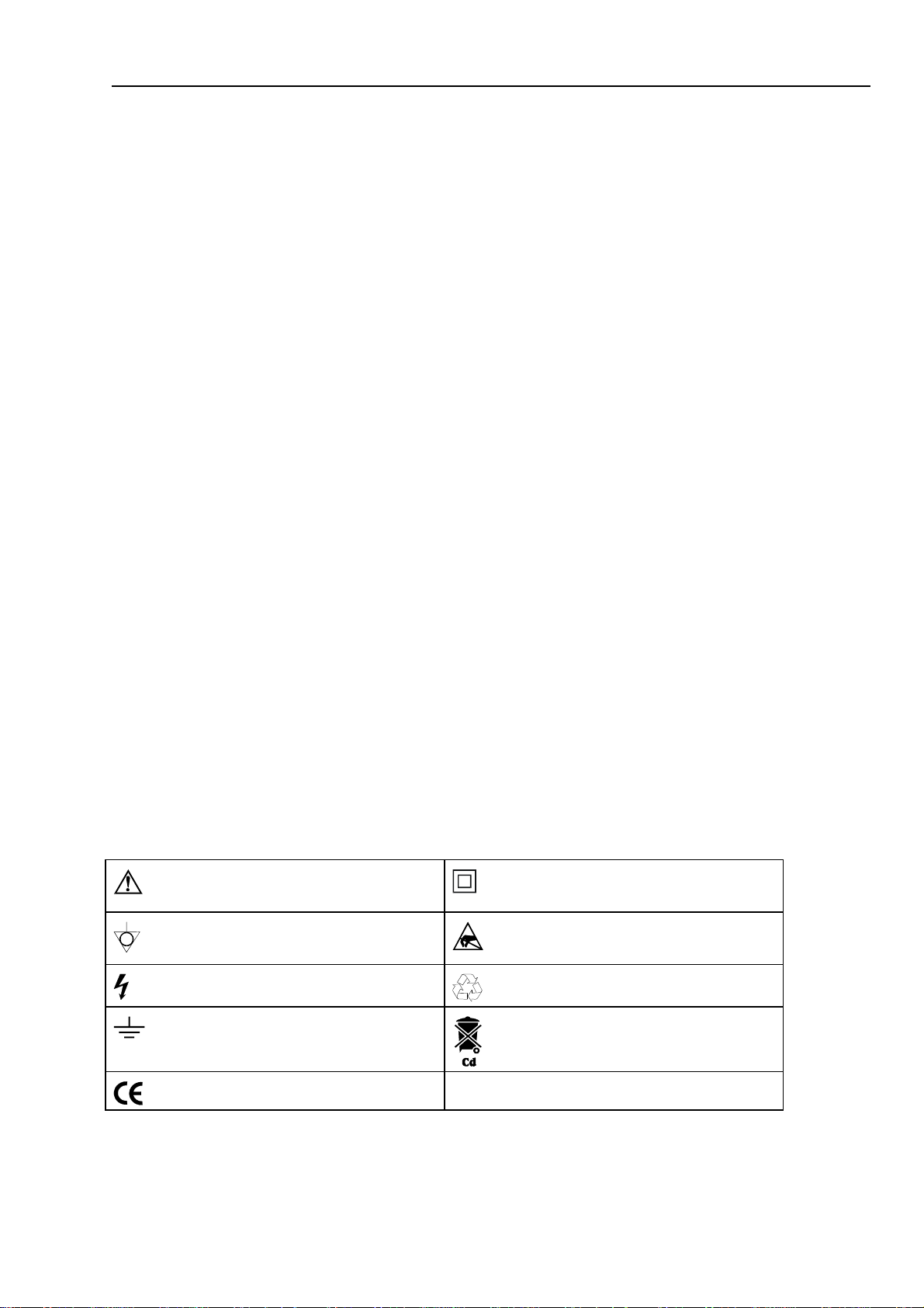
Table 1-1 shows the symbols used on the test tool or in this manual.
Table 1-1. Symbols
Read the safety information in the Users
Manual
Equal potential inputs, connected
internally
Live voltage Recycling information
DOUBLE INSULATION (Protection Class)
Static sensitive components
(black/yellow).
Earth Disposal information
Conformité Européenne
1-3
Page 14

43B
Service Manual
1.5 Impaired Safety
1.6 General Safety Information
Whenever it is likely that safety has been impaired, the instrument must be turned off
and disconnected from line power. The matter should then be referred to qualified
technicians. Safety is likely to be impaired if, for example, the instrument fails to
perform the intended measurements or shows visible damage.
Warning
Removing the instrument covers or removing parts, except
those to which access can be gained by hand, is likely to
expose live parts and accessible terminals which can be
dangerous to life.
The instrument shall be disconnected from all voltage sources before it is opened.
Capacitors inside the instrument can hold their charge even if the instrument has been
separated from all voltage sources.
Components which are important for the safety of the instrument may only be replaced
by components obtained through your local FLUKE organization. These parts are
indicated with an asterisk (*) in the List of Replaceable Parts, Chapter 8.
1-4
Page 15

Chapter 2
Characteristics
Title Page
2.1 Introduction................................................................................................. 2-3
2.2 Safety Specifications................................................................................... 2-3
2.3 Function Specifications............................................................................... 2-4
2.3.1 Electrical functions.............................................................................. 2-4
2.3.2 Scope.................................................................................................... 2-5
2.3.3 Meter.................................................................................................... 2-7
2.3.4 Record.................................................................................................. 2-7
2.4 Miscellaneous ............................................................................................. 2-8
2.5 Current Probe .............................................................................................. 2-8
2.6 Environmental Conditions .......................................................................... 2-9
2.7 Electromagnetic Immunity.......................................................................... 2-10
2-1
Page 16

Page 17

2.1 Introduction
Safety Characteristics
The Fluke 43B has been designed and tested in accordance with Standards ANSI/ISA
S82.01-1994, EN 61010.1 (1993) (IEC 1010-1), CAN/CSA-C22.2 No.1010.1-92
(including approval), UL3111-1 (including approval) Safety Requirements for
Electrical Equipment for Measurement, Control, and Laboratory Use.
This manual contains information and warnings that must be followed by the user to
ensure safe operation and to keep the instrument in a safe condition. Use of this
equipment in a manner not specified by the manufacturer may impair protection
provided by the equipment.
Performance Characteristics
FLUKE guarantees the properties expressed in numerical values with the stated
tolerance. Specified non-tolerance numerical values indicate those that could be
nominally expected from the mean of a range of identical ScopeMeter test tools.
Environmental Data
The environmental data mentioned in this manual are based on the results of the
manufacturer’s verification procedures.
Characteristics
2.1 Introduction
2
2.2 Safety Specifications
Safety Characteristics
Designed and tested for measurements on 600 Vrms Category III, Pollution Degree 2
in accordance with:
• EN 61010.1 (1993) (IEC 1010-1)
• ANSI/ISA S82.01-1994
• CAN/CSA-C22.2 No.1010.1-92 (including approval)
• UL3111-1 (including approval)
Installation Category III refers to distribution level and fixed installation circuits
inside a building.
Maximum input voltage Input 1 and 2
Direct on inputs or with test leads TL24 ............................................... (see Figure 2-1)
0 to 66 kHz ................................................................................................. 600 Vrms
> 66 kHz ....................................................................................... derating to 5 Vrms
With Shielded Banana-to-BNC Adapter Plug BB120 ...........................(see Figure 2-1)
0 to 400 kHz ............................................................................................... 300 Vrms
> 400 kHz ..................................................................................... derating to 5 Vrms
2-3
Page 18

43B
Service Manual
Figure 2-1. Max. Input Voltage vs. Frequency
Maximum floating voltage
From any terminal to ground
0 to 400 Hz ................................................................................................. 600 Vrms
2.3 Function Specifications
The accuracy of all measurements is within ± (% of reading + number of counts) from
18 °C to 28 °C. For all specifications, probe specifications must be added.
2.3.1 Electrical functions
Specifications are valid for signals with a fundamental between 40 and 70 Hz.
Minimum input voltage ................................................................................. 4 V peak-peak
Minimum input current............................................................... 10 A peak-peak (1 mV/A)
Input bandwidth................................................ DC to 15 kHz (unless specified otherwise)
Volts / Amps / Hertz
Readings ..................................................................... Vrms (ac+dc), Arms (ac+dc), Hz
Voltage ranges (auto) ....................................................... 5 V; 50 V; 500 V; 1250 V
minimum step.............................................................. 1 mV; 10 mV; 100 mV; 1 V
Current ranges (auto)..................................................50.00 A to 500.0 kA, 1250 kA
minimum step........................................................10 mA; 0.1 A; 1 A; 100 A, 1 kA
Frequency range .........................................................................10.0 Hz to 15.0 kHz
40.0 to 70.0 Hz......................................................................... ±(0.5 % + 2 counts)
resolution.................................................................... 0.1 Hz; 1 Hz; 10 Hz; 100 Hz
CF Crest Factor range....................................................1.0 to 10.0 ±(5 % + 1 count)
ST8571
±(1 % + 10 counts)
±(1 % + 10 counts)
2-4
Power (1 and 3 phase / 3 conductor / balanced loads)
Readings ..........................................................................Watt, VA, VAR, PF, DPF, Hz
Watt, VA, VAR ranges (auto) .....................250 W to 250 MW, 625 MW, 1.56 GW
when selected: total ( %r):........................................................ ±(2 % + 6 counts)
when selected: fundamental ( %f):........................................... ±(4 % + 4 counts)
DPF.......................................................................................................... 0.00 to 1.00
0.00 to 0.25........................................................................................not specified
0.25 to 0.90.................................................................................................. ± 0.04
0.90 to 1.00.................................................................................................. ± 0.03
Page 19

Characteristics
2.3 Function Specifications
PF............................................................................................................. 0.00 to 1.00
Frequency range .........................................................................10.0 Hz to 15.0 kHz
40.0 to 70.0 Hz ...................................................................... ±(0.5 % + 2 counts)
Harmonics
Number of harmonics ................................................................DC..21, DC..33, DC..51
Readings / Cursor readings
Vrms....fund. ±(3 % + 2 counts) ..... 31
Irms......fund. ±(3 % + 2 counts) ..... 31
Watt.....fund. ±(5 % + 10 counts) ... 31
st
±(5 % + 3 counts)..... 51st ±(15 % + 5 counts)
st
±(5 % + 3 counts)..... 51st ±(15 % + 5 counts)
st
±(10 % + 10 counts) 51st ±(30 % + 5 counts)
Frequency of fundamental.......................................................................... ± 0.25 Hz
Phase........................................................................................fund. ±3° ... 51
K-factor (in Amp and Watt) ............................................................................± 10 %
Sags & Swells
Recording times (selectable) .............................. 4 minutes to 8 days, endless (16 days)
Readings / Cursor Readings
Vrms actual, Arms actual (cycle by cycle calculation) ............... ±(2 % + 10 counts)
Vrms max, Arms max (idem at cursor) ....................................... ±(2 % + 12 counts)
Vrms average, Arms average (only at cursor)............................. ±(2 % + 10 counts)
Vrms min, Arms min (idem at cursor) ........................................ ±(2 % + 12 counts)
± 0.04
st
± 15°
2
Transients
Detection of voltage transients ............................................................................ > 40 ns
Useful input bandwidth input 1 (with test leads TL24)..............................DC to 1 MHz
Reference signal ...............................................................................................Vrms, Hz
Detection when transients exceed specified voltage level (selectable)
Number of transient memories (temporary) ................................................................ 40
Cursor reading
Inrush
Graphic display
Cursor readings
2.3.2 Scope
Input Impedance
Input 1............................................ 1 MΩ // 12 pF (± 2 pF). With BB120: 20 pF ± 3 pF
Input 2............................................ 1 MΩ // 10 pF (± 2 pF). With BB120: 18 pF ± 3 pF
After START, the Vrms and frequency of the signal are measured.
From these data a pure sine wave is calculated.
Voltage levels ...................................20 %, 50 %, 100 %, 200 % of reference signal
Vpeak min, Vpeak max at cursor ..................................................± 5 % of full scale
Current ranges (selectable).................. 1 A, 5 A, 10 A, 50 A, 100 A, 500 A, 1000 A
Inrush times (selectable)........................................... 1 s, 5 s, 10 s, 50 s, 100 s, 5 min
A peak max at cursor 1..................................................................± 5 % of full scale
A peak max at cursor 2..................................................................± 5 % of full scale
Time between cursors.................................................................. ±(0.2 % + 2 pixels)
Horizontal
Time base modes (selectable)......................................................... Normal, Single, Roll
Ranges (selectable within modes)
In Normal............................................................................................ 5 s to 20 ns/div
In Single shot........................................................................................5 s to 1 µs/div
In Roll mode ......................................................................................... 60 s to 1 s/div
Time base error................................................................................< ±(0.4 % + 1 pixel)
2-5
Page 20

43B
Service Manual
Maximum sampling rate
10 ms to 60 s....................................................................................................5 MS/s
20 ns to 10 ms................................................................................................25 MS/s
Trigger source (auto, ½ auto, manual)................................................. Input 1 or Input 2
Trigger
Mode.........................................................................................................auto triggering
Sources........................................ Input 1, Input 2, Automatic (not manually selectable)
Error for frequencies < 1 MHz
Voltage Level ...............................................................................................± 0.5 div
at positive slope the top of the trigger symbol and at negative trigger the bottom of
the trigger symbol is the trigger point.
Time Delay Real Time sampling...............................................................± 1 sample
Time Delay Quasi Random sampling............................................................. ± 10 ns
Sensitivity input 1
@ 40 MHz ....................................................................................................... ≥ 4 div
@ 25 MHz .................................................................................................... ≥ 1.5 div
@ DC - 5 MHz................................................................................≥ 0.5 div or 5 mV
Sensitivity input 2
@ DC – 20 kHz ............................................................................................≥ 0.5 div
Slope Selection ....................................................................................Positive, negative
Level Control
Range Manual control .............................................> ± 4 div, within dynamic range
Delay ( horizontal move ) ..........-10 div - 0 div, used for horizontal move functionality
Vertical
Voltage ranges .............................................................................5 mV/div to 500 V/div
Trace accuracy................................................................................ ±(1 % + 2 pixels)
Bandwidth input 1 (voltage)
excluding test leads or probes ................................................DC to 20 MHz (-3 dB)
with test leads TL24 .................................................................DC to 1 MHz (-3 dB)
with 10:1 probe VPS100-R (optional).................................... DC to 20 MHz (-3 dB)
with shielded test leads STL120 (optional)......................... DC to 12.5 MHz (-3 dB)
DC to 20 MHz (-6 dB)
Lower transition point (ac coupling).................................................... 10 Hz (-3 dB)
Bandwidth input 2 (current)
with Banana-to-BNC adapter ...............................................................DC to 15 kHz
Lower transition point (ac coupling).................................................... 10 Hz (-3 dB)
Scope readings
The accuracy of all scope readings is valid from 18 °C to 28 °C with relative humidity
up to 90 % for a period of one year after calibration. Add 0.1 x (the specified
accuracy) for each °C below 18 °C or above 28 °C. More than one waveform period
must be visible on the screen.
V dc, A dc ........................................................................................ ±(0.5 % + 5 counts)
V ac and V ac+dc (True RMS) input 1
DC to 60 Hz................................................................................. ±(1 % + 10 counts)
60 Hz to 20 kHz........................................................................ ±(2.5 % + 15 counts)
20 kHz to 1 MHz ......................................................................... ±(5 % + 20 counts)
1 MHz to 5 MHz........................................................................ ±(10 % + 25 counts)
5 MHz to 20 MHz...................................................................... ±(30 % + 25 counts)
A ac and A ac+dc (True RMS) input 2
DC to 60 Hz................................................................................. ±(1 % + 10 counts)
60 Hz to 15 kHz......................................................................... ±(30 % + 25 counts)
Frequency (Hz), Pulse width, Duty cycle (2.0 % to 98.0 %)
2-6
Page 21

Phase (Input 1 to Input 2)
Peak voltage
Crest
2.3.3 Meter
Ohm
Ranges.........................................................................500.0 Ω to 5.000 MΩ, 30.00 MΩ
Max. Measurement Current..................................................................................0.5 mA
Measurement Voltage at open circuit..................................................................... < 4 V
Characteristics
2.3 Function Specifications
1 Hz to 1 MHz ............................................................................ ±(0.5 % + 2 counts)
1 MHz to 10 MHz.......................................................................... ±(1 % + 2 counts)
10 MHz to 30 MHz..................................................................... ±(2.5 % + 2 counts)
Up to 60 Hz............................................................................................................±2°
60 Hz to 400 Hz.....................................................................................................±5°
Peak max, Peak min.......................................................................± 5 % of full scale
Peak-peak.....................................................................................± 10 % of full scale
Range......................................................................................................... 1.0 to 10.0
±(5 % + 1 count)
±(0.6 % + 5 counts)
2
Diode
Accuracy.............................................................................................. ±(2 % +5 counts)
Max. Measurement Current..................................................................................0.5 mA
Measurement Voltage at open circuit..................................................................... < 4 V
Continuity
Beep .........................................................................................................< 30 Ω (± 5 Ω)
Measurement Current ...........................................................................................0.5 mA
Detection of shorts.................................................................................................> 1 ms
Capacitance
Ranges.............................................................................................50.00 nF to 500.0 µF
Max. Measurement Current..................................................................................0.5 mA
Temperature
Ranges (°C or °F) ........................................-100.0 to +400.0 °C or -200.0 to +800.0 °F
2.3.4 Record
Record times (selectable) ...............................................4 min to 8 days, endless (16 days)
Number of readings ............................................................................1 or 2 simultaneously
Record is available for the functions:
• volts / amps / hertz
• power
• harmonics
• ohms / continuity / capacitance
• temperature
• scope
±(2 % +10 counts)
±(0.5 % + 5 counts)
2-7
Page 22

43B
Service Manual
2.4 Miscellaneous
Display
Useful screen area............................................................... 72 x 72 mm (2.83 x 2.83 in)
Resolution..............................................................................................240 x 240 pixels
Backlight................................................................... Cold Cathode Fluorescent (CCFL)
Power
External
Power Adapter ...............................................................................................PM8907
Input Voltage .........................................................................................10 to 21 V dc
Power........................................................................................................5 W typical
Internal
Rechargeable Ni-Cd battery pack.....................................................................BP120
Voltage range.............................................................................................4 to 6 V dc
Operating Time............................................................................................... 4 hours
Charging Time.................................................................4 hours with Fluke 43B off
12 hours with Fluke 43B on
Refresh cycle ......................................................................................... 8 to 14 hours
Memory
Number of screen memories........................................................................................ 20
Number of transient memories (temporary) ................................................................ 40
Mechanical
Height x width x depth ......................................... 232 x 115 x 50 mm (9.1 x 4.5 x 2 in)
Weight (including battery pack)...............................................................1.1 kg (2.5 lb.)
Interface....................................................................................... RS232, optically isolated
Supported Printers ........................HP Deskjet
Serial via PM9080 (optically isolated RS232 Adapter/Cable).
Parallel via PAC91 (optically isolated Print Adapter Cable, optional).
To PC........................................................................... Dump and load settings and data
Serial via PM9080 (optically isolated RS232 adapter/cable),
using SW43W (FlukeView
2.5 Current Probe
Safety Characteristics
Designed for measurements on 600 Vrms Category III. Protection class II, double or
reinforced insulation requirements in accordance with:
• IEC 1010-1
• ANSI/ISA S82
• CSA-C22.2 No.1010.1-92
• UL1244
®
, Laserjet®, PostScript and Epson FX80
®
Power Quality Analyzer software).
2-8
Electrical Specifications
Current range .........................................................................................1 A to 500 Arms
AC current over range limit..............................................................................700 Arms
Maximum 10 minutes, followed by removal from current carrying conductor
for 30 minutes.
Output Signal............................................................................................. 1 mV ac/A ac
Page 23

Characteristics
2.6 Environmental Conditions
Accuracy
5 to 10 Hz
1 to 500 A ............................................................................................-3 dB typically
10 to 20 Hz
1 to 300 A ..........................................................................................................± 5 %
300 to 400 A ....................................................................................................± 15 %
400 to 500 A ....................................................................................................± 25 %
20 to 45 Hz
1 to 500 A ..........................................................................................................± 5 %
45 to 65 Hz
1 to 20 A .............................................................................. ±5 % of reading + 0.3 A
20 to 100 A ........................................................................................±5 % of reading
± 3 ° phase shift
100 to 500 A ......................................................................................±2 % of reading
± 5 ° phase shift
65 Hz to 3 kHz
1 to 50 A ............................................................................................. ±(5 % + 0.4 A)
50 to 500 A ........................................................................................................± 5 %
Influence of temperature on accuracy ................................... <0.15 % per 10 °C (18 °F)
Altitude
During operation.................................................................................2.0 km (6560 feet)
While stored......................................................................................12 km (40 000 feet)
2
2.6 Environmental Conditions
Environmental ..................................................... MIL 28800E, Type 3, Class III, Style B
Temperature
During operation...................................................................... 0 to 50 °C (32 to 122 °F)
While stored...........................................................................-20 to 60 °C (-4 to 140 °F)
Humidity
During operation:
0 to 10 °C (32 to 50 °F) ...................................................................non-condensing
10 to 30 °C (50 to 86 °F) .........................................................................95 % ± 5 %
30 to 40 °C (86 to 104 °F) ........................................................................75 % ± 5 %
40 to 50 °C (104 to 122 °F) ......................................................................45 % ± 5 %
While stored:
-20 to 60 °C (-4 to 140 °F).................................................................non-condensing
Altitude
During operation..............................................................................4.5 km (15 000 feet)
The maximum input and floating voltage is 600 Vrms up to 2 km.
Linearly derating from 600 down to 400 Vrms between 2 km to 4.5 km.
While stored......................................................................................12 km (40 000 feet)
Vibration.................................................................................................................max. 3 g
Shock.....................................................................................................................max. 30 g
Electromagnetic Compatibility (EMC)
Emission ............................................... EN 50081-1 (1992): EN55022 and EN60555-2
Immunity.................................................... EN 50082-2 (1992): IEC1000-4-2, -3, -4, -5
(See also Tables 2-1 to 2-3)
Enclosure Protection ............................................................................. IP51, ref.: IEC529
2-9
Page 24
43B
Service Manual
2.7 Electromagnetic Immunity
The Fluke 43B, including standard accessories, conforms with the EEC directive 89/336
for EMC immunity, as defined by IEC1000-4-3, with the addition of the following tables.
Disturbance with test leads TL24 or Current Clamp 80i-500s
• Volts / amps / hertz
• Resistance, Capacitance
• Power
• Harmonics
Table 2-1. No Visible Disturbance
No visible disturbance E = 3 V/m E = 10 V/m
Frequency: 10 kHz - 27 MHz
Frequency: 27 MHz - 1 GHz
(-)
(-)
(-): no visible disturbance
Disturbance with test leads TL24 in scope mode
• V ac+dc (True RMS)
Table 2-2. Disturbance < 1 %
Disturbance less than 1 %
of full scale
Frequency: 10 kHz - 27 MHz
Frequency: 27 MHz - 200 MHz
Frequency: 200 MHz - 1 GHz
E = 3 V/m E = 10 V/m
2 V/div - 500 V/div
500 mV/div - 500V/div
(-)
(-): no visible disturbance
Table 2-3. Disturbance < 10 %
Disturbance less than 10 %
of full scale
Frequency: 10 kHz - 27 MHz
Frequency: 27 MHz - 200 MHz
E = 3 V/m E = 10 V/m
1 V/div
200 mV/div
(-)
(-)
10 V/div - 500 V/div
2 V/div - 500 V/div
5 mV/div - 500 V/div
5 V/div
1 V/div
2-10
Frequency: 200 MHz - 1 GHz
(-)
(-)
(-): no visible disturbance
Ranges not specified in Tables 2 and 3 may have a disturbance of more than 10 % of full
scale.
Page 25

Chapter 3
Circuit Descriptions
Title Page
3.1 Introduction................................................................................................. 3-3
3.2 Block Diagram ............................................................................................ 3-3
3.2.1 Input 1 - Input 2 Measurement Circuits............................................... 3-3
3.2.2 Trigger Circuit ..................................................................................... 3-5
3.2.3 Digital Circuit ...................................................................................... 3-5
3.2.4 Power Circuit....................................................................................... 3-6
3.2.5 Start-up Sequence, Operating Modes .................................................. 3-7
3.3 Detailed Circuit Descriptions...................................................................... 3-9
3.3.1 Power Circuit....................................................................................... 3-9
3.3.2 Input 1 - Input 2 Measurement Circuits............................................... 3-15
3.3.3 Trigger Circuit ..................................................................................... 3-20
3.3.4 Digital Circuit ...................................................................................... 3-24
3-1
Page 26
43B
Service Manual
3-2
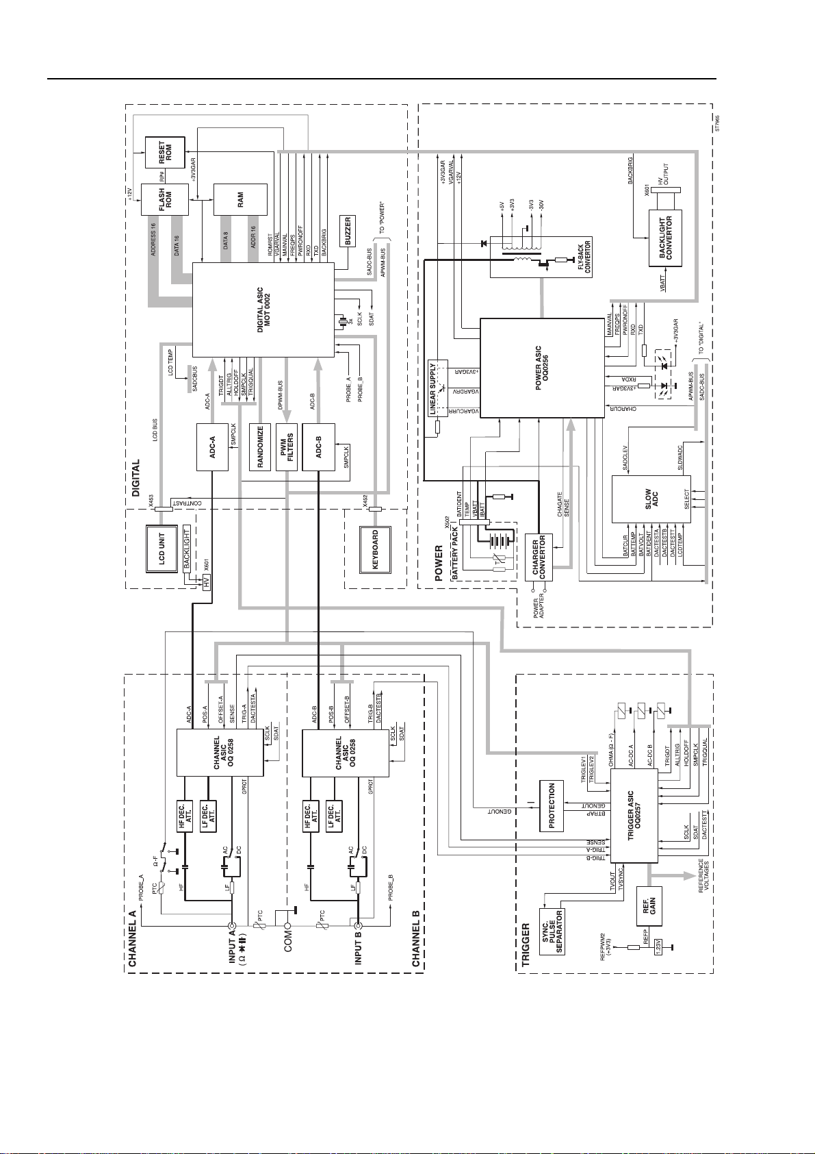
Figure 3-1. Fluke 43B Block Diagram
ST7965.EPS
Page 27

3.1 Introduction
Section 3.2 describes the functional block diagram shown in Figure 3-1. It provides a
quick way to get familiar with the test tool basic build-up.
Section 3.3 describes the principle of operation of the test tool functions in detail, on the
basis of the circuit diagrams shown in Figures 9-1 to 9-5.
For all measurements, input signals are applied to the shielded input banana jackets.
Traces and readings are derived from the same input signal samples.
3.2 Block Diagram
In the block diagram Figure 3-1, the test tool is divided in five main blocks. Each block
represents a functional part, build up around an Application Specific Integrated Circuit
(ASIC). A detailed circuit diagram of each block is shown in Section 9.
Table 3-1 provides an overview of the blocks in which the test tool is broken down, the
main block function, the ASIC name, and the applicable circuit diagram.
Circuit Descriptions
3.1 Introduction
3
Table 3-1. Fluke 43B Main Blocks
Block Main Functions ASIC Circuit
Diagram
INPUT 1 Input 1 signal conditioning C(hannel)-ASIC OQ0258 Figure 9-1
INPUT 2 Input 2 signal conditioning C(hannel)-ASIC OQ0258 Figure 9-2
TRIGGER Trigger selection and conditioning
Current source for resistance, capacitance,
continuity, and diode measurements
AC/DC input coupling and Ω/F relay control
Voltage reference source
DIGITAL Analog to Digital Conversion
Acquisition of ADC samples
Micro controller (µP-ROM-RAM)
Keyboard- and LCD control
POWER Power supply, battery charger
LCD back light voltage converter
Optical interface input
T(rigger)-ASIC OQ0257 Figure 9-3
D(igital)-ASIC MOT0002 Figure 9-4
P(ower)-ASIC OQ0256 Figure 9-5
All circuits, except the LCD unit and the KEYBOARD, are located on one Printed
Circuit Board (PCB), called the MAIN PCB.
The ASIC’s are referred to as C-ASIC (Channel ASIC), T-ASIC (Trigger ASIC), P-ASIC
(Power ASIC), and D-ASIC (Digital ASIC).
3.2.1 Input 1 - Input 2 Measurement Circuits
The basic input signal for the Input 1 and Input 2 circuits (hardware) is voltage. The
reading of Input 1 is in (milli)Volts. The reading of Input 2 is in Amperes. So the
voltage on Input 2 is assumed to be supplied by a current clamp. From the measured
voltage samples the readings are calculated by the instrument firmware. For example:
power readings are calculated from the Input 1 and Input 2 voltage samples.
3-3
Page 28

43B
Service Manual
The Input 1 and Input 2 measurement circuits are partially identical. The differences are:
• Only Input 1 provides facilities for Ohms, Continuity, Diode, and Capacitance
measurements.
• The bandwidth of the Input 1 circuit is 20 MHz, the bandwidth of Input 2 is 15 kHz.
• Input 2 has an additional hum rejection circuit.
The circuit description below applies to the Input 1 and Input 2 circuit.
Input 1 and Input 2 measurement principle
An input voltage applied to Input 1 or Input 2 is supplied to the C-ASIC via the HF path
(Input 1 only) and the LF path. Depending on the actual measurement function the
Input-1 HF path in the C-ASIC is enabled or disabled. The HF DECade ATTenuator and
LF DECade ATTenuator are external components for the HF and LF path. The C-ASIC
converts (attenuates, amplifies) the input signal to a normalized output voltage
ADC-A/ADC-B, which is supplied to the Analog to Digital Converters (ADC-A and
ADC-B) on the DIGITAL part. The D-ASIC acquires the digital samples to build the
traces, and to calculate readings.
For the electrical functions the current Input 2 circuit is operating in low voltage ranges.
For example a current of 10A measured with a 1 mV/A current clamp generates 10 mV
(voltage range 10 mV/div). To minimize the influence of interference voltages, Input 2
has no HF path, and has an additional hum reject circuit.
The lowest Input 1 voltage range for electrical measurements is 4V/div, which is high in
comparison with the Input 2 range.
Ohms, Continuity, and Diode measurement function (Input 1 only)
The T-ASIC supplies a current via the Ω/F relays to the unknown resistance Rx or diode
connected to the Input 1 and the COM input jacket. The voltage drop across Rx or the
diode is measured according to the Input 1 measurement principle.
Capacitance measurement function (Input 1 only)
The T-ASIC supplies a current via the Ω/F relays to the unknown capacitance Cx,
connected to the Input 1 and the COM input jacket. Cx is charged and discharged by this
current. The C-ASIC converts the charging time and the discharging time into a pulse
width signal. This signal is supplied to the T-ASIC via the C-ASIC trigger output
TRIG-A. The T-ASIC shapes and levels the signal, and supplies the resulting pulse
width signal ALLTRIG to the D-ASIC. The D-ASIC counts the pulse width and
calculates the capacitance reading.
Scope measurement function
In the Scope measurements function the test tool shows the traces and readings derived
from the input signals. The Input 1 HF path is enabled, which results in a 20 MHz
bandwidth. The Input 2 bandwidth is 15 kHz.
Other measurement functions
Volts/Amperes/Hertz (LF), Power (LF), Harmonics (LF), Sags & Swells (LF),
Transients, Inrush Current (LF), and Temperature measurement results are calculated
from acquired input voltage samples. For functions with (LF), the HF path of Input 1 is
disabled, which results in a 15 kHz bandwidth for both Input channels.
3-4
Miscellaneous
Control of the C-ASIC, e.g. selecting the attenuation factor, is done by the D-ASIC via
the SDAT and SCLK serial communication lines.
Page 29

An offset compensation voltage and a trace position control voltage are provided by the
D-ASIC via the APWM bus.
The C-ASIC’s also provide conditioned input voltages on the TRIG-A/TRIG-B line. One
of these voltages will automatically be selected as trigger source by the T-ASIC.
3.2.2 Trigger Circuit
The T ASIC selects one of the possible trigger sources TRIG-A (Input 1) or TRIG-B
(Input 2). For triggering on transients the selected trigger source signal is processed via
the high pass Trigger Filter (TVOUT-TVSYNC lines). Two adjustable trigger levels are
supplied by the D-ASIC via the PWM FILTERS (TRIGLEV1 and TRIGLEV2 line).
Depending on the selected trigger conditions (- source, - level, - edge, - mode), the
T-ASIC generates the final trigger signal TRIGDT, which is supplied to the D-ASIC.
The TRIG-A input is also used for capacitance measurements (see Section 3.2.1).
The T-ASIC includes a constant current source for resistance and capacitance
measurements. The current is supplied via the GENOUT output and the Ω/F relays to
the unknown resistance Rx or capacitance Cx connected to Input 1. The SENSE signal
senses the voltage across Cx and controls a CLAMP circuit in the T-ASIC. This circuit
limits the voltage on Input 1 at capacitance measurements. The protection circuit
prevents the T-ASIC from being damaged by voltages supplied to the input during
resistance or capacitance measurements.
Circuit Descriptions
3.2 Block Diagram
3
The T-ASIC contains opamps to derive reference voltages from a 1.23 V reference
source. The gain factors for these opamps are determined by resistors in the REF GAIN
circuit. The reference voltages are supplied to various circuits.
The T-ASIC also controls the Input 1/2 AC/DC input coupling relays, and the Ω/F relay.
Control data for the T-ASIC are provided by the D-ASIC via the SDAT and SCLK serial
communication lines.
3.2.3 Digital Circuit
The D-ASIC includes a micro processor, ADC sample acquisition logic, trigger logic,
display and keyboard control logic, I/O ports, and various other logic circuits.
The instrument software is stored in the 8M FlashROM; the 4M RAM is used for
temporary data storage.
For Voltage and Resistance measurements, the conditioned Input 1/2 voltages are
supplied to the ADC-A and ADC-B ADC. The voltages are sampled, and digitized by
the ADC’s. The output data of the ADC’s are acquired and processed by the D-ASIC.
For capacitance measurements the pulse width of the T-ASIC output signal ALLTRIG,
which is proportional to the unknown capacitance, is counted by the D-ASIC.
The DPWM-BUS (Digital Pulse Width Modulation) supplies square wave signals with a
variable duty cycle to the PWM FILTERS circuit (RC filters). The outgoing
APWM-BUS (Analog PWM) provides analog signals of which the amplitude is
controlled by the D-ASIC. These voltages are used to control e.g. the trace positions
(C-ASIC), the trigger levels (T-ASIC), and the battery charge current (P-ASIC).
In random sampling mode (Scope mode time base faster than 1 µs/d), a trace is built-up
from several acquisition cycles. During each acquisition, a number of trace samples are
placed as pixels in the LCD. The RANDOMIZE circuit takes care that the starting
moment of each acquisition cycle (trigger release signal HOLDOFF goes low) is random.
3-5
Page 30

43B
Service Manual
This prevents that at each next acquisition the trace is sampled at the same time
positions, and that the displayed trace misses samples at some places on the LCD.
The D-ASIC supplies control data and display data to the LCD module. The LCD
module is connected to the main board via connector X453. It consists of the LCD, LCD
drivers, and a fluorescent back light lamp. As the module is not repairable, no detailed
description and diagrams are provided. The back light supply voltage is generated by the
back light converter on the POWER part.
The keys of the keyboard are arranged in a matrix. The D-ASIC drives the rows and
scans the matrix. The contact pads on the keyboard foil are connected to the main board
via connector X452. The ON-OFF key is not included in the matrix, but is sensed by a
logic circuit in the D-ASIC, that is active even when the test tool is turned off.
Via the PROBE-A and PROBE-B lines, connected to the Input 1 and Input 2 banana
shielding, the D-ASIC can detect if a probe is connected.
The D-ASIC sends commands to the C-ASICs and T-ASIC via the SCLK and SDAT
serial control lines, e.g. to select the required trigger source.
Various I/O lines are provided, e.g. to control the BUZZER and the Slow-ADC (via the
SADC bus).
3.2.4 Power Circuit
The test tool can be powered via the power adapter, or by the battery pack.
If the power adapter is connected, it powers the test tool and charges the battery via the
CHARGER-CONVERTER circuit. The battery charge current is sensed by sense
resistor Rs (signal IBAT). It is controlled by changing the output current of the
CHARGER-CONVERTER (control signal CHAGATE).
If no power adapter is connected, the battery pack supplies the VBAT voltage. The
VBAT voltage powers the P-ASIC, and is also supplied to the FLY BACK
CONVERTER (switched mode power supply).
If the test tool is turned on, the FLY BACK CONVERTER generates supply voltages for
various test tool circuits.
The +3V3GAR supply voltage powers the D-ASIC, RAM and ROM. If the test tool is
turned off, the battery supplies the +3V3GAR voltage via transistor V569. This
transistor is controlled by the P-ASIC. So when the test tool is turned off, the D-ASIC
can still control the battery charging process (CHARCURR signal), the real time clock,
the on/off key, and the serial RS232 interface (to turn the test tool on).
To monitor and control the battery charging process, the P-ASIC senses and buffers
battery signals as temperature (TEMP), voltage (BATVOLT), current (IBAT).
Via the SLOW ADC various analog signals can be measured by the D-ASIC. Involved
signals are: battery voltage (BATVOLT), battery type (IDENT), battery temperature
(TEMP), battery current (BATCUR) LCD temperature (LCDTEMP, from LCD unit),
and 3 test output pins of the C-ASIC’s, and the T-ASIC (DACTEST). The signals are
used for control and test purposes.
3-6
The BACK LIGHT CONVERTER generates the 400V ! supply voltage for the LCD
fluorescent back light lamp. If the lamp is defective a 1.5 kV voltage can be present for
0.2 second maximum. The brightness is controlled by the BACKBRIG signal supplied
by the D-ASIC.
Serial communication with a PC or printer is possible via the RS232 optically isolated
interface. The P-ASIC buffers the received data line (RXDA) and supplies the buffered
data (RXD) to the D-ASIC. The transmit data line TXD is directly connected to the
D-ASIC.
Page 31

3.2.5 Start-up Sequence, Operating Modes
The test tool sequences through the next steps when power is applied (see Figure 3-2):
1. The P-ASIC is directly powered by the battery or power adapter voltage VBAT.
Initially the Fly Back Converter is off, and the D-ASIC is powered by VBAT via
transistor V569 (+3V3GAR).
If the voltage +3V3GAR is below 3.05 V, the P-ASIC keeps its output signal
VGARVAL (supplied to the D-ASIC) low, and the D-ASIC will not start up. The
test tool is not working, and is in the Idle mode.
2. If the voltage +3V3GAR is above 3.05 V, the P-ASIC makes the line VGARVAL
high, and the D-ASIC will start up. The test tool is operative now. If it is powered
by batteries only, and not turned on, it is in the Off mode. In this mode the
D-ASIC is active: the real time clock runs, and the ON/OFF key is monitored to see
if the test tool will be turned on.
3. If the power adapter is connected (P-ASIC output MAINVAL high), and/or the
test tool is turned on, the embedded D-ASIC program, called mask software, starts
up. The mask software checks if valid instrument software is present in the Flash
ROM. If not, the test tool does not start up and the mask software continues running
until the test tool is turned off, or the power is removed. This is called the Mask
active mode. The mask active mode can also be entered by pressing the ^ and > key
when turning on the test tool.
Circuit Descriptions
3.2 Block Diagram
3
If valid instrument software is present, one of the following modes becomes active:
Charge mode
The Charge mode is entered when the test tool is powered by the power adapter,
and is turned off. The FLY-BACK CONVERTER is off. The CHARGER-
CONVERTER charges the batteries (if installed).
Operational & Charge mode
The Operational & Charge mode is entered when the test tool is powered by the
power adapter, and is turned on. The FLY-BACK CONVERTER is on, the
CHARGER-CONVERTER supplies the primary current. If batteries are installed,
they will be charged. In this mode a battery refresh (see below) can be done.
Operational mode
The Operational mode is entered when the test tool is powered by batteries only,
and is turned on. The FLY-BACK CONVERTER is on, the batteries supply the
primary current. If the battery voltage (VBAT) drops below 4V when starting up the
fly back converter, the Off mode is entered.
Battery Refresh
Each 3 months the batteries need a deep discharge-full charge cycle, called a
“refresh”. This prevents battery capacity loss due to the memory effect. A refresh
cycle takes 16 hours maximum, depending on the battery status.
A refresh can be started via the keyboard (
SETUP
power adapter is connected. During a refresh, first the batteries are completely
discharged, and then they are completely charged again.
=> START BATTERY REFRESH ) if the test tool is on, and the
=>
=>
I=> INSTRUMENT
3-7
Page 32

43B
Service Manual
VGARVAL=L
VGARVAL=H
Idle mode
Off mode
TURN ON or
MAINVAL=H
Flash ROM
Mask StartUp
Flash ROM OK
Extern StartUp
NOT OK
OR
& TURN ON&
MAINVAL=L & (TURN OFF or BATTVOLT<4V)
Software
TURN ON & BATTVOLT > 4 & MAINVAL=L TURN OFF&MAINVAL=H
TURN ON & MAINVAL=H
Operational
Mode
MAINVAL=H
Operational &
Charge Mode
MAINVAL=L TURN ON
TURN OFF
Mask Active
mode
Charge Mode
TURN OFF
BATTVOLT < 4V
or
AutoShutDown
or
TURN OFF
Battery refresh
MAINVAL=L
Figure 3-2. Fluke 43B Start-up Sequence, Operating Modes
Table 3-2 shows an overview of the test tool operating modes.
Table 3-2. Fluke 43B Operating Modes
Mode Conditions Remark
Idle mode No power adapter and no battery no activity
Off mode No power adapter connected, battery
installed, test tool off
Mask active mode No valid instrument software, or ^ and > key
pressed when turning on
Charge mode Power adapter connected and test tool off Batteries will be charged
Operational &
Power adapter connected and test tool on Test tool operational, and
Charge mode
Operational mode No power adapter connected, battery
installed, and test tool on
P-ASIC & D-ASIC powered
(VBAT & +3V3GAR).
Mask software runs
batteries will be charged
Test tool operational, powered
by batteries
3-8
Page 33

3.3 Detailed Circuit Descriptions
R
E
P
P
P
E
R
P
R
L
T
P
2
7
7
C
3.3.1 Power Circuit
The description below refers to circuit diagram Figure 9-5.
Power Sources , Operating Modes
Figure 3-3 shows a simplified diagram of the power supply and battery charger circuit.
VBAT
FROM POWER
ADAPTER
R501
R502
C502
CHARGER/CONVERTER
V506
V503
L501
C503
R504
R506
R507
R503
R512
R514
R516
R513
VGARDRIVE
VBATSU
VBATHIGH
VBAT
TEM
TEMPHI
IBAT
CHAGAT
CHASENSN
CHASENS
IIMAXCHA
VCHDRI V
VADALOW
VADAPTE
60
3
5
4
9
16
14
15
6
19
8
20
V569
69 66
Vref
CONTROL
linear regulator
linear regulator
Circuit Descriptions
3.3 Detailed Circuit Descriptions
VGARVA
BATVOLT
BATTEM
BATCU
CHARCUR
43
COS
V565
V566
P7VCHA
SUPPLY
+3V3GAR
C553
MAI NVAL
C507
CONVERTER
Amplify
Level shift
100kHz
FLY BACK
64
78
79
7
80
1
18
18
3
POWER ASIC
Figure 3-3. Power Supply Block Diagram
As described in Section 3.2.5, the test tool operating mode depends on the connected
power source.
The voltage VBAT is supplied either by the power adapter via V506/L501, or by the
battery pack. It powers a part of the P-ASIC via R503 to pin 60 (VBATSUP). If the test
tool is off, the Fly Back Converter is off, and VBAT powers the D-ASIC via transistor
V569 (+3V3GAR). This +3V3GAR voltage is controlled and sensed by the P-ASIC. If
it is NOT OK (<3.05V), the output VGARVAL (pin 64) is low. The VGARVAL line is
connected to the D-ASIC, and if the line is low, the D-ASIC is inactive: the test tool is in
the Idle mode. A low VGARVAL line operates as a reset for the D-ASIC.
If VGARVAL is high (+3V3GAR > 3.05V), the D-ASIC becomes active, and the Off
mode is entered. The D-ASIC monitors the P-ASIC output pin 12 MAINVAL, and the
test tool ON/OFF status. By pressing the ON/OFF key, a bit in the D-ASIC indicating
the test tool ON/OFF status is toggled. If no correct power adapter voltage is supplied
(MAINVAL is low), and the test tool is not turned on, the Off mode will be maintained.
If a correct power adapter voltage is supplied (MAINVAL high), or if the test tool is
turned on, the mask software starts up. The mask software checks if valid instrument
software is present. If not, e.g. no instrument firmware is loaded, the mask software will
3-9
Page 34

43B
Service Manual
keep running, and the test tool is not operative: the test tool is in the Mask active state.
For test purposes the mask active mode can also be entered by pressing the ^ and > key
when the test tool is turned on.
If valid software is present, one of the three modes Operational, Operational &
Charge or Charge will become active. The Charger/Converter circuit is active in the
Operational & Charge and in the Charge mode. The Fly back converter is active in the
Operational and in the Operational & Charge mode.
Charger/Converter (See also Figure 3-3.)
The power adapter powers the Charge Control circuit in the P-ASIC via an internal linear
regulator. The power adapter voltage is applied to R501. The Charger/Converter circuit
controls the battery charge current. If a charged battery pack is installed VBAT is
approximately +4.8V. If no battery pack is installed VBAT is approximately +15V. The
voltage VBAT is supplied to the battery pack, to the P-ASIC, to the Fly Back Converter,
and to transistor V569. The FET control signal CHAGATE is a 100 kHz square wave
voltage with a variable duty cycle, supplied by the P-ASIC Control circuit. The duty
cycle determines the amount of energy loaded into L501/C503. By controlling the
voltage VBAT, the battery charge current can be controlled. The various test tool
circuits are supplied by the Fly Back Converter and/or V569.
Required power adapter voltage
The P-ASIC supplies a current to reference resistor R516 (VADALOW pin 8). It
compares the voltage on R516 to the power adapter voltage VADAPTER on pin 20
(supplied via R502, and attenuated in the P-ASIC). If the power adapter voltage is below
10V, the P-ASIC output pin 12, and the line MAINVAL, are low. This signal on pin 12
is also supplied to the P-ASIC internal control circuit, which then makes the CHAGATE
signal high. As a result FET V506 becomes non-conductive, and the Charger/Converter
is off.
Battery charge current control
The actual charge current is sensed via resistors R504-R506-507, and filter R509-C509,
on pin 9 of the P-ASIC (IBATP). The sense voltage is supplied to the control circuit.
The required charge current information is supplied by the D-ASIC via the CHARCUR
line and filter R534-C534 to pin 80. A control loop in the control circuit adjusts the
actual charge current to the required value.
The filtered CHARCUR voltage range on pin 80 is 0... 2.7V for a charge current from
0.5A to zero. A voltage of 0V complies to 0.5A (fast charge), 1.5V to 0.2A (top off
charge), 2.3V to 0.06A (trickle charge), and 2.7V to 0A (no charge). If the voltage is > 3
Volt, the charger converter is off (V506 permanently non-conductive).
The D-ASIC derives the required charge current value from the battery voltage VBAT.
The P-ASIC converts this voltage to an appropriate level and supplies it to output pin 78
(BATVOLT). The D-ASIC measures this voltage via the Slow ADC. The momentary
value, and the voltage change as a function of time (-dV/dt), are used as control
parameters.
3-10
Charging process
If the battery voltage drops below 5.2V, and the battery temperature is between 10 and
45°C, the charge current is set to 0.5A (fast charge). From the battery voltage change dV/dt the D-ASIC can see when the battery is fully charged, and stop fast charge.
Additionally a timer in the D-ASIC limits the fast charge time to 6 hours. After fast
charge, a 0.2A top off charge current is supplied for 2 hours. Then a 0.06A trickle
Page 35

Circuit Descriptions
3.3 Detailed Circuit Descriptions
charge current is applied for 48 hours maximum. If the battery temperature becomes
higher than 50°C, the charge current is set to zero.
Battery temperature monitoring
The P-ASIC supplies a current to a NTC resistor in the battery pack (TEMP pin 5). It
conditions the voltage on pin 5 and supplies it to output pin 79 BATTEMP. The D-ASIC
measures this voltage via the slow ADC. It uses the BATTEMP voltage to decide if fast
charge is allowed (10-45°C), or no charge is allowed at all (<10°C, >50°C).
Additionally the temperature is monitored by the P-ASIC. The P-ASIC supplies a
current to reference resistor R512 (TEMPHI pin 4), and compares the resulting TEMPHI
voltage to the voltage on pin 5 (TEMP). If the battery temperature is too high, the
P-ASIC Control circuit sets the charge current to zero, in case the D-ASIC fails to do
this.
If the battery temperature monitoring system fails, a bimetal switch in the battery pack
interrupts the battery current if the temperature becomes higher then 70 °C.
Maximum VBAT
The P-ASIC supplies a current to reference resistor R513 (VBATHIGH pin 7). It
compares the voltage on R513 to the battery voltage VBAT on pin 3 (after being
attenuated in the P-ASIC). The P-ASIC limits the voltage VBAT to 7.4V via its internal
Control circuit. This happens if no battery or a defective battery (open) is present.
3
Charger/Converter input current
This input current is sensed by R501. The P-ASIC supplies a reference current to R514.
The P-ASIC compares the voltage drop on R501 (P-ASIC pin 14 and 15) to the voltage
on R514 (IMAXCHA pin 6). It limits the input current (e.g. when loading C503/C555
just after connecting the power adapter) via its internal Control circuit.
CHAGATE control signal
To make the FET conductive its Vgs (gate-source voltage) must be negative. For that
purpose, the CHAGATE voltage must be negative with respect to VCHDRIVE. The
P-ASIC voltage VCHDRIVE also limits the swing of the CHAGATE signal to 13V.
VCHDRIVE
VCHDRIVE -13V
10 µs
Figure 3-4. CHAGATE Control Voltage
V506 “OFF”
V506 “ON”
+3V3GAR Voltage
When the test tool is not turned on, the Fly Back Converter does not run. In this
situation, the +3V3GAR voltage for the D-ASIC, the FlashROM, and the RAM is
supplied via transistor V569. The voltage is controlled by the VGARDRV signal
supplied by the P-ASIC (pin 69). The current sense voltage across R580 is supplied to
pin 70 (VGARCURR). The voltage +3V3GAR is sensed on pin 66 for regulation. The
internal regulator in the P-ASIC regulates the +3V3GAR voltage, and limits the current.
3-11
Page 36

43B
Service Manual
Fly Back Converter
When the test tool is turned on, the D-ASIC makes the PWRONOFF line (P-ASIC pin
62) high. Then the self oscillating Fly Back Converter becomes active. It is started up
by the internal 100 kHz oscillator that is also used for the Charger/Converter circuit.
First the FLYGATE signal turns FET V554 on (see Figure 3-5), and an increasing
current flows in the primary transformer winding to ground, via sense resistor R551. If
the voltage FLYSENSP across this resistor exceeds a certain value, the P-ASIC turns
FET V554 off. Then a decreasing current flows in the secondary windings to ground. If
the windings are “empty” (all energy transferred), the voltage VCOIL sensed by the
P-ASIC (pin 52) is zero, and the FLYGATE signal will turn FET V554 on again.
Primary current
Secondary current
V554 “ON”
FLYGATE SIGNAL
Figure 3-5. Fly-Back Converter Current and Control Voltage
V554 “OFF”
The output voltage is regulated by feeding back a part of the +3V3A output voltage via
R552-R553-R554 to pin 54 (VSENS). This voltage is referred to a 1.23 V reference
voltage. Any deviation of the +3V3A voltage from the required 3.3V changes the
current level at which current FET V554 will be switched off. If the output voltage
increases, the current level at which V554 is switched off will become lower, and less
energy is transferred to the secondary winding. As a result the output voltage will
become lower.
An internal current source supplies a current to R559. The resulting voltage is a
reference for the maximum allowable primary current (IMAXFLY). The voltage across
the sense resistor (FLYSENSP) is compared to the IMAXFLY voltage. If the current
exceeds the set limit, FET V554 will be turned off.
Another internal current source supplies a current to R558. This resulting voltage is a
reference for the maximum allowable output voltage (VOUTHI). The -3V3A output
voltage (M3V3A) is attenuated and level shifted in the P-ASIC, and then compared to
the VOUTHI voltage. If the -3V3A voltage exceeds the set limit, FET V554 will be
turned off.
The FREQPS control signal is converted to appropriate voltage levels for the FET switch
V554 by the BOOST circuit. The voltage VBAT supplies the BOOST circuit power via
V553 and R561. The FREQPS signal is also supplied to the D-ASIC, in order to detect
if the Fly Back converter is running well.
V551 and C552 limit the voltage on the primary winding of T552 when the FET V554 is
turned of. The signal SNUB increases the FLYGATE high level to decreases
ON-resistance of V554 (less power dissipation in V554).
3-12
Page 37

VBAT
C
V553
8
R561
T552
Circuit Descriptions
3.3 Detailed Circuit Descriptions
+5VA
V561
V562
+3V3A
3
C553
COS
FLYBOOST
C551
43
SNUB
48 47
BOOST
CONTROL
C552
49
63
55
57
44
52
5
51
54
62
72
FLYGATE
FREQPS
FLYSENSP
IMAXFLY
VCOIL
-3V3A
VOUTHI
VSENS
PWRONOFF
REFP (1.23V)
V551
V554
R551
R559
R558
V563
V564
R570
-3V3A
-30VD
R552
R554
R553
POWER ASIC
Figure 3-6. Fly-Back Converter Block Diagram
Slow ADC
The Slow ADC enables the D-ASIC to measure the following signals:
BATCUR, BATVOLT, BATTEMP, BATIDENT (Battery current, - voltage, temperature, - type ), DACTEST-A, DACTEST-B, and DACTEST-T (test output of the
C-ASIC’s and the T-ASIC).
De-multiplexer D531 supplies one of these signals to its output, and to the input of
comparator N531 TP536). The D-ASIC supplies the selection control signals
SELMUX0-2. The Slow ADC works according to the successive approximation
principle. The D-ASIC changes the SADCLEV signal level, and thus the voltage level
on pin 3 of the comparator step wise, by changing the duty cycle of the PWM signal
SADCLEVD. The comparator output SLOWADC is monitored by the D-ASIC, who
knows now if the previous input voltage step caused the comparator output to switch. By
increasing the voltage steps, the voltage level can be approximated within the smallest
possible step of the SADCLEV voltage. From its set SADCLEVD duty cycle, the DASIC knows voltage level of the selected input.
RS232
The optical interface enables serial communication (RS232) between the test tool and a
PC or printer.
The received data line RXDA (P-ASIC pin 75) is connected to ground via a 20 kΩ
resistor in the P-ASIC.
If no light is received by the light sensitive diode H522, the RXDA line is +200 mV,
which corresponds to a “1” (+3V) on the RXD (P-ASIC output pin 76) line.
If light is received, the light sensitive diode will conduct, and the RXDA line goes low
(0...-0.6V), which corresponds to a “0” on the RXD line.
The level on the RXDA line is compared by a comparator in the P-ASIC to a 100 mV
level. The comparator output is the RXD line, which is supplied to the D-ASIC for
communication, and for external triggering.
3-13
Page 38

43B
Service Manual
The D-ASIC controls the transmit data line TXD. If the line is low, diode H521 will
emit light.
The supply voltage for the optical interface receive circuit (RXDA), is the +3V3SADC
voltage. The +3V3SADC voltage is present if the test tool is turned on, or if the Power
Adapter is connected (or both). So if the Power Adapter is present, serial
communication is always possible, even when the test tool is off.
Backlight Converter
The LCD back light is provided by a ∅2.4 mm fluorescent lamp in LCD unit. The back
light converter generates the 300-400 Vpp ! supply voltage. The circuit consist of:
• A pulse width modulated (PWM) buck regulator to generate a variable, regulated
voltage (V600, V602, L600, C602).
• A zero voltage switched (ZVS) resonant push-pull converter to transform the
variable, regulated voltage into a high voltage AC output (V601, T600).
The PWM buck regulator consists of FET V600, V602, L600, C602, and a control circuit
in N600. FET V600 is turned on and off by a square wave voltage on the COUT output
of N600 pin 14). By changing the duty cycle of this signal, the output on C602 provides
a variable, regulated voltage. The turn on edge of the COUT signal is synchronized with
each zero detect.
Outputs AOUT and BOUT of N600 provide complementary drive signals for the pushpull FETs V601a/b (dual FET). If V601a conducts, the circuit consisting of the primary
winding of transformer T600 and C608, will start oscillating at its resonance frequency.
After half a cycle, a zero voltage is detected on pin 9 (ZD) of N600, V601a will be
turned off, and V601b is turned on. This process goes on each time a zero is detected.
The secondary current is sensed by R600/R604, and fed back to N600 pin 7 and pin 4 for
regulation of the PWM buck regulator output voltage. The BACKBRIG signal supplied
by the D-ASIC provides a pulse width modulated (variable duty cycle) square wave. By
changing the duty cycle of this signal, the average on-resistance of V604 can be changed.
This will change the secondary current, and thus the back light intensity. The voltage on
the “cold” side of the lamp is limited by V605 and V603. This limits the emission of
electrical interference.
R605 and R606 provide a more reliable start-up of the backlight (PCB version 3 up
only).
Voltage at T600 pin 4
Voltage AOUT
Voltage BOUT
Voltage COUT
3-14
zero
detect
zero
detect
Figure 3-7. Back Light Converter Voltages
Page 39

3.3.2 Input 1 - Input 2 Measurement Circuits
The description below refers to circuit diagrams Figure 9-1 and Figure 9-2.
The Input 1 and Input 2 circuits are partly identical. Both circuits condition input
voltages. See section 3.2.1 for a description of the differences between Input 1 and 2.
The Input 1/2 circuitry is built-up around a C-ASIC OQ0258. The C-ASIC is placed
directly behind the input connector and transforms the input signal to levels that are
suitable for the ADC and trigger circuits.
The C-ASIC
Figure 3-8 shows the simplified C-ASIC block diagram. The C-ASIC consists of
separate paths for HF and LF signals, an output stage that delivers signals to the trigger
and ADC circuits and a control block that allows software control of all modes and
adjustments. The transition frequency from the LF-path to the HF-path is approximately
20 kHz, but there is a large overlap.
3.3 Detailed Circuit Descriptions
CHANNEL ASIC OQ 0258
Circuit Descriptions
3
INPUT
C
AC
R
DC
HF IN
LF IN
GROUND
PROTECT
Figure 3-8. C-ASIC Block Diagram
HF-PATH
LF-PATH
CAL POS BUS SUPPLY
OUTPUT
STAGE
CONTROL SUPPLY
ADC
TRIGGER
LF input
The LF-input (pin 42) is connected to a LF decade attenuator in voltage mode, or to a
high impedance buffer for resistance and capacitance measurements. The LF decade
attenuator consists of an amplifier with switchable external feedback resistors R131 to
R136. Depending on the selected range the LF attenuation factor which will be set to 110-100-1000-10,000. The C-ASIC includes a LF pre-amplifier with switchable gain
factors for the 1-2-5 steps.
HF input (not used for Input 2)
The HF component of the input signal is supplied to four external HF capacitive
attenuators via C104. Depending on the required range, the C-ASIC selects and buffers
one of the attenuator outputs :1 (HF0), :10 (HF1), :100 (HF2), or :1000 (HF3). By
attenuating the HF3 input internally by a factor 10, the C-ASIC can also create a :10000
attenuation factor. Inputs of not selected input buffers are internally shorted. To control
the DC bias of the buffers inputs, their output voltage is fed back via an internal feed
back resistor and external resistors R115, R111/R120, R112, R113, and-R114. The
internal feed back resistor and filter R110/C105 will eliminate HF feed back, to obtain a
3-15
Page 40

43B
Service Manual
large HF gain. The C-ASIC includes a HF pre-amplifier with switchable gain factors for
the 1-2-5 steps. The C-ASIC also includes circuitry to adjust the gain, and pulse
response.
ADC output pin 27
The combined conditioned HF/LF signal is supplied to the ADC output (pin 27) via an
internal ADC buffer. The output voltage is 150 mV/d. The MIDADC signal (pin 28),
supplied by the ADC, matches the middle of the C-ASIC output voltage swing to the
middle of the ADC input voltage swing.
TRIGGER output pin 29
The combined conditioned HF/LF signal is also supplied to the trigger output (pin 29)
via an internal trigger buffer. The output voltage is 100 mV/d. This signal (TRIG-A) is
supplied to the TRIGGER ASIC for triggering, and for capacitance measurements.
For capacitance measurements the ADC output is not used, but the TRIG-A output pulse
length indicates the measured capacitance, see “Capacitance measurements” below.
GPROT input pin 2
PTC (Positive Temperature Coefficient) resistors (R106-R206) are provided between the
Input 1 and Input 2 shield ground, and the COM input (instrument ground). This
prevents damage to the test tool if the various ground inputs are connected to different
voltage levels. The voltage across the PTC resistor is supplied via the GPROT input pin
2 to an input buffer. If this voltage exceeds ±200 mV, the ground protect circuit in the
C-ASIC makes the DACTEST output (pin 24) high. The DACTEST line output level is
read by the D-ASIC via the slow ADC (See 3.3.2 “Power”). The test tool will give a
ground error warning.
Because of ground loops, a LF interference voltage can arise across PTC resistor R106
(mainly mains interference when the power adapter is connected). To eliminate this LF
interference voltage, it is buffered (also via input GPROT, pin 2), and subtracted from
the input signal. Pin 43B (PROTGND) is the ground reference of the input buffer.
CALSIG input pin 36
The reference circuit on the TRIGGER part supplies an accurate +1.23 V DC voltage to
the CALSIG input pin 36 via R141. This voltage is used for internal calibration of the
gain, and the capacitance measurement threshold levels. A reference current Ical is
supplied by the T-ASIC via R144 for calibration of the resistance and capacitance
measurement function. For ICAL see also Section 3.3.3.
POS input pin 1
The PWM circuit on the Digital part provides an adjustable voltage (0 to 3.3 V) to the
POS input via R151. The voltage level is used to move the input signal trace on the
LCD. The REFN line provides a negative bias voltage via R152, to create the correct
voltage swing level on the C-ASIC POS input.
OFFSET input pin 44
The PWM circuit on the Digital part supplies an adjustable voltage (0 to +3.3 V) to the
OFFSET input via R153. The voltage level is used to compensate the offset in the LF
path of the C-ASIC. The REFN line provides a negative bias voltage via R152, to create
the correct voltage swing level on the C-ASIC POS input.
3-16
Page 41

Circuit Descriptions
3.3 Detailed Circuit Descriptions
DACTEST output pin 24
As described above, the DACTEST output is used for signaling a ground protect error. It
can also be used for testing purposes. Furthermore the DACTEST output provides a CASIC reset output signal (+1.75V) after a power on.
ADDRESS output pin 23
The output provides a replica of the input voltage to the SENSE line via R165. In
capacitance mode, the sense signal controls the CLAMP function in the T-ASIC (See
Section 3.3.3).
TRACEROT input pin 31
The TRACEROT signal is supplied by the T-ASIC. It is a triangle sawtooth voltage.
SDAT, SCLK
Control information for the C-ASIC, e.g. selection of the attenuation factor, is sent by the
D-ASIC via the SDA data line. The SCL line provides the synchronization clock signal.
Input 1 Voltage Measurements
The input voltage is applied to the HF attenuator inputs of the C-ASIC via C104, and to
the LF input of the C-ASIC via R101/R102, AC/DC input coupling relay K171, and
R104. The C-ASIC conditions the input voltage to an output voltage of 50 mV/d. This
voltage is supplied to the ADC on the Digital part. The ADC output data is read and
processed by the D-ASIC, and represented as a numerical reading, and as a graphical
trace.
3
Table 3-3. shows the relation between the Input 1 reading range (V) and the trace
sensitivity (V/d.) in the Scope mode. The selected trace sensitivity determines the
C-ASIC attenuation/gain factor. The reading range is only a readout function, it does not
change the hardware range or the wave form display.
Table 3-3. Input 1 Voltage Ranges And Trace Sensitivity
range 50 mV 50 mV 50 mV 500 mV 500 mV 500 mV 5V 5V
trace ../div 5 mV 10 mV 20 mV 50 mV 100 mV 200 mV 500 mV 1V
range 5V 50V 50V 50V 500V 500V 500V 1250V
trace ../div 2V 5V 10V 20V 50V 100V 200V 500V
During measuring, input voltage measurements, gain measurements, and zero
measurements are done. As a result, the voltage supplied to the ADC is a multiplexed
(zero, + reference, -reference, input voltage) signal. In ROLL mode however, no gain
and zero measurements are done. Now the ADC input voltage includes only the
conditioned input voltage.
The input voltage is connected to Input 1. The shield of the input is connected to system
ground (⊥⊥⊥⊥) via a PTC ground protection resistor. If a voltage is applied between the
Input 1 and Input 2 ground shield, or between one of these ground shields and the black
COM input, the PTC resistor will limit the resulting current. The voltage across the PTC
resistor is supplied to the C-ASIC GPROT input, and causes a ground error warning
(high voltage level) on output pin 24 (DACTEST).
Input 2 Voltage Measurements
The Input 2 circuit has no HF path. The principle of operation is the same as for the
Input 1 LF path. The input ground is connected via PTC resistor R201 to the
3-17
Page 42

43B
Service Manual
measurement ground. Any voltage across the PTC resistor will be added to the input
signal, and cause a mis-reading. This influences Input 2 in particular as this input
operates mostly in the lowest voltage ranges (see section 3.2.1). For this reason a hum
rejection circuit is added for Input 2. The voltage across the PTC is supplied to the
inverting X1 amplifier N202. Then the AC part of the N202 output signal is subtracted
from the input sigal on the C-ASIC LF input (pin 42).
Resistance Measurements (Input 1 only)
The unknown resistance Rx is connected to Input 1, and the black COM input. The
T-ASIC supplies a constant current to Rx via relay contacts K173, and the PTC resistor
R172. The voltage across Rx is supplied to a high impedance input buffer in the C-ASIC
via the LF input pin 42. The C-ASIC conditions the voltage across Rx to an output
voltage of 50 mV/d. This voltage is supplied to the ADC on the Digital part. The ADC
data is read and processed by the D-ASIC, and represented as a numerical reading, and a
bar graph.
Table 3-4 shows the relation between the reading range (Ω), the trace sensitivity (Ω/d.),
and the current in Rx,
Table 3-4. Ohms Ranges, Trace Sensitivity, and Current
Range 50Ω 500Ω 5kΩ 50 kΩ 500 kΩ 5 MΩ 30 MΩ
Sensitivity ../div 20Ω 200Ω 2 kΩ 20 kΩ 200 kΩ 2 MΩ 10 MΩ
Current in Rx 500 µA 500 µA 50 µA5 µA 500 nA 50 nA 50 nA
To protect the current source from being damaged by a voltage applied to the input, a
PTC resistor R172 and a protection circuit are provided (See Section 3.3.3 “Current
Source”).
During measuring, input voltage measurements, gain measurements, and zero
measurements are done. As a result, the voltage supplied to the ADC is a multiplexed
(zero, + reference, -reference, input voltage) signal.
Capacitance Measurements (Input 1 only)
The capacitance measurement is based on the equation: C x dV = I x dt. The unknown
capacitor Cx is charged with a constant known current. The voltage across Cx increases,
and the time lapse between two different known threshold crossings is measured. Thus
dV, I and dt are known and the capacitance can be calculated.
The unknown capacitance Cx is connected to the red Input 1 safety banana socket, and
the black COM input. The T-ASIC supplies a constant current to Cx via relay contacts
K173, and protection PTC resistor R172. The voltage on Cx is supplied to two
comparators in the C-ASIC via the LF input. The threshold levels th
and th2of the
1
comparators are fixed (see Figure 3-9). The time lapse between the first and the second
threshold crossing depends on the value of Cx. The resulting pulse is supplied to the
TRIGGER output pin 29, which is connected to the analog trigger input of the T-ASIC
(TRIG-A signal). The T-ASIC adjusts the pulse to an appropriate level, and supplies it
to the D-ASIC via its ALLTRIG output. The pulse width is measured and processed by
the D-ASIC, and represented on the LCD as numerical reading. There will be no trace
displayed.
3-18
Page 43

+Ire
f
-Iref
ref clamp
th2
Circuit Descriptions
3.3 Detailed Circuit Descriptions
0
pos. clamp active
I-Cx
3
th1
0
neg. clamp active neg. clamp active
U-Cx
TRIG-A
Figure 3-9. Capacitance Measurement
The T-ASIC supplies a positive (charge) and a negative (discharge) current. A
measurement cycle starts from a discharged situation (U
After reaching the first threshold level (th
) the pulse width measurement is started. The
1
=0) with a charge current.
CX
dead zone between start of charge and start of pulse width measurement avoids
measurement errors due to a series resistance of Cx.
The pulse width measurement is stopped after crossing the second threshold level (th
),
2
the completes the first part of the cycle.
Unlimited increase of the capacitor voltage is avoided by the positive clamp in the
T-ASIC. The output of the high impedance buffer in the C-ASIC supplies a replica of
the voltage across Cx to output pin 23 (ADDRESS). Via R165, this voltage is supplied
to a clamp circuit in the T-ASIC (SENSE, pin 59). This clamp circuit limits the positive
voltage on Cx to 0.45V.
Now the second part of the measurement is started by reversing the charge current. The
capacitor will be discharged in the same way as the charge cycle. The time between
passing both threshold levels is measured again. A clamp limits the minimum voltage on
Cx to 0V.
Averaging the results of both measurements cancels the effect of a possible parallel
resistance, and suppresses the influence of mains interference voltages.
Table 3-5 shows the relation between the capacitance ranges, the charge current and the
pulse width at full scale.
Table 3-5. Capacitance Ranges, Current, and Pulse Width
Range 50 nF 500 nF 5000 nF 50 µF 500 µF
Current µA0.5 µA5 µA 50 µA 500 µA 500 µA
Pulse width at Full Scale 25 ms 25 ms 25 ms 25 ms 250 ms
To protect the current source if a voltage is applied to the input, a PTC resistor R172,
and a protection circuit on the TRIGGER part, are provided (see Section 3.3.3).
Probe Detection
The Input 1 and Input 2 safety banana jacks are provided with a ground shield, consisting
of two separated half round parts. One half is connected to ground via the protection
PTC resistor R106/R206. Via a 220K resistor installed on the input block, the other half
is connected to the probe input of the D-ASIC (pin 54, 55). If the shielded STL120 test
3-19
Page 44
43B
A
Service Manual
3.3.3 Trigger Circuit
lead, or a BB120 shielded banana-to-BNC adapter, is inserted in Input 1 or Input 2, it
will short the two ground shield halves This can be detected by the D-ASIC.
Supply Voltages
The +5VA, +3V3A, and -3V3A supply voltages are supplied by the Fly Back Converter
on the POWER part. The voltages are present only if the test tool is turned on.
The description refers to circuit diagram Figure 9-3. The trigger section is built up
around the T-ASIC OQ0257. It provides the following functions:
• Triggering: trigger source selection, trigger signal conditioning, and generation of
trigger information to be supplied to the D-ASIC.
• Current source for resistance and capacitance measurements.
• Voltage reference source: buffering and generation of reference voltages.
• AC/DC relay and Resistance/Capacitance (Ω/F) relay control.
Triggering
Figure 3-10 shows the block diagram of the T-ASIC trigger section.
trigger section
select
logic
freq.
detect
synchronize
delta-t
35
ALLTRIG
42
TRIGQUAL
34
TRIGDT
39
HOLDOFF
38
SMPCLK
29
DACTEST
TRIGLEV1
TRIGLEV2
TRIG A
TRIG B
10
11
13
15
Figure 3-10. T-ASIC Trigger Section Block Diagram
TRIGGER ASIC OQ0257
analog
path
trigger
16
TVSYNC
High pass
filter
LLTRIG
DUALTRI G
12
TVOUT
The analog trigger path uses the Input 1 (TRIG A) or Input 2 (TRIG B) signal for
triggering.
In the Transients mode the TRIG A or TRIG B signal is routed via a high pass filter
(TVOUT - TVSYNC). The High Pass Filter consists of C395 and R399.
The TRIG-A, TRIG-B, or TVSYNC signal, and two trigger level voltages TRIGLEV1
and TRIGLEV2, are supplied to the analog trigger part. The trigger level voltages are,
supplied by the PWM section on the Digital part (See Section 3.3.4). The TRIGLEV1
voltage is used for triggering on a negative slope of the Input 1/2 voltage. The
TRIGLEV2 voltage is used for triggering on a positive slope of the Input 1/2 voltage. As
the C-ASIC inverts the Input 1/2 voltage, the TRIGA, TRIGB slopes on the T-ASIC
input are inverted! From the selected trigger source signal and the used trigger level
voltages, the ALLTRIG and the DUALTRIG trigger signal are derived. The select logic
selects which one will be used by the synchronization/delta-T circuit to generate the final
trigger. There are three possibilities:
3-20
Page 45

Circuit Descriptions
3.3 Detailed Circuit Descriptions
1. Single shot triggering.
The DUALTRIG signal is supplied to the synchronization/delta-T circuit. The
trigger levels TRIGLEV1 and TRIGLEV2 are set just above and below the DC level
of the input signal. A trigger is generated when the signal crosses the trigger levels.
A trigger will occur on both a positive or a negative glitch. This mode ensures
triggering, when the polarity of an expected glitch is not known.
2. Qualified triggering .
The ALLTRIG signal is supplied to T-ASIC output pin 35, which is connected to the
D-ASIC input pin 21. The D-ASIC derives a qualified trigger signal TRIGQUAL
from ALLTRIG, e.g. on each 10th ALLTRIG pulse a TRIGQUAL pulse is given.
The TRIGQUAL is supplied to the synchronize/delta-T circuit via the select logic.
3. Normal triggering.
The ALLTRIG signal is supplied to the synchronization/delta-T circuit.
The ALLTRIG signal includes all triggers. It is used by the D-ASIC for signal analysis
during AUTOSET.
Traditionally a small trigger gap is applied for each the trigger level. In noisy signals,
this small-gap-triggering would lead to unstable displaying of the wave form, if the noise
is larger than the gap. The result is that the system will trigger randomly. This problem
is solved by increasing the trigger gap (TRIGLEV1 - TRIGLEV2) automatically to 80%
(10 to 90%) of the input signal peak-to-peak value. This 80% gap is used in AUTOSET.
3
Note
The ALLTRIG signal is also used for capacitance measurements (S. 3.3.2).
The Synchronize/Delta-t part provides an output pulse TRIGDT. The front edge of this
pulse is the real trigger moment. The pulse width is a measure for the time between the
trigger moment, and the moment of the first sample after the trigger. This pulse width
information is required in random repetitive sampling mode (see below). The
HOLDOFF signal, supplied by the D-ASIC, releases the trigger system. The sample
clock SMPCLK, also provided by the D-ASIC, is used for synchronization.
Real time sampling TRIGDT signal
For time base settings of 1 µs/d and slower, the pixel distance on the LCD is ≥40 ns (1
division is 25 pixels). As the maximum sample rate is 25 MHz, a sample is taken each
40 ns. So the first sample after a trigger can be assigned to the first pixel, and successive
samples to each next pixel. A trace can be built-up from a single period of the input
signal.
Random repetitive (equivalent) sampling TRIGDT signal
For time base settings below 1 µs/d, the time between two successive pixels on the
screen is smaller than the time between two successive samples. For example at 20 ns/d,
the time between two pixels is 20:25=0.8 ns, and the sample distance is 40 ns (sample
rate 25 MHz). A number of sweeps must be taken to reconstruct the original signal, see
Figure 3-11. As the samples are taken randomly with respect to the trigger moment, the
time dt must be known to position the samples on the correct LCD pixel. The TRIGDT
signal is a measure for the time between the trigger and the sample moment dt. The
pulse duration of the TRIGDT signal is approximately 4 µs...20 µs.
3-21
Page 46

43B
Service Manual
TRIGGER
SAMPLES SWEEP 1
SAMPLES SWEEP 2
PIXEL
Figure 3-11. Random Repetitive Sampling Mode
3
dt1
4
dt2
21346591078 11
13
14
14
1512 13 16
DACTEST output
A frequency detector in the T-ASIC monitors the ALLTRIG signal frequency. If the
frequency is too high to obtain a reliable transmission to the D-ASIC, the DACTEST
output pin 29 will become high. The DACTEST signal is read by the D-ASIC via the
slow ADC on the Power part. It and indicates that the D-ASIC cannot use the ALLTRIG
signal (e.g. for qualified triggering).
Current Source
A current source in the T-ASIC supplies a DC current to the GENOUT output pin 1. The
current is used for resistance and capacitance measurements. It is adjustable in decades
between 50 nA and 500 µA depending on the measurement range, and is derived from an
external reference current. This reference current is supplied by the REFP reference
voltage via R323 and R324 to input REFOHMIN (pin 6).
The SENSE input signal is the buffered voltage on Input 1. For capacitance
measurements it is supplied to a clamp circuit in the T-ASIC (pin 59). The clamp circuit
limits the positive voltage on the unknown capacitance to 0.45V.
The protection circuit prevents the T-ASIC from being damaged by a voltage applied to
Input 1 during resistance or capacitance measurements. If a voltage is applied, a current
will flow via PTC resistor R172 (on the Input 1 part), V358/V359, V353, V354 to
ground. The resulting voltage across the diodes is approximately -2V or +15V.
R354/R356, and V356/V357 limit the voltage on the T-ASIC GENOUT output (pin 1).
The BOOTSTRAP output signal on pin 3 is the buffered GENOUT signal on pin 1, or
the buffered SENSE signal on pin 59. It is supplied to the protection diodes via R352,
R353, and to protection transistor V356, to minimize leakage currents.
On the ICAL-output of the T-ASIC (pin 5) a copy of the output current on GENOUT is
available. The current is supplied to the Input 1 C-ASIC via R144. As ICAL shows the
same time/temperature drift as the GENOUT measurement current, it can be used for
internal calibration of the resistance and capacitance measurement function.
Capacitor C356 is used for hum/noise suppression.
3-22
Page 47

Circuit Descriptions
2
655576364
453
2518
2
P
M
F
N
N
3.3 Detailed Circuit Descriptions
Reference Voltage Circuit
This circuit derives several reference voltages from the 1.23 V main reference source.
3
+3.3V
+3.3V
-1.23V
+0.1V
+1.23V
R309
R311
R312
R308
R306
R310
R303
R307
V301
1.23V
REFPWM2
REFP
REF
GAINPW
REFPWM1
GNDRE
GAINREF
REF
GAINADCB
REFADCB
73
P-ASIC
OQ0256
7
71
6
5
5
+
-
T-ASIC
+
1
-
+
2
-
+
3
-
OQ0257
+
+1.6V
R302
R301
R305
GAINADCT
REFADCT
REFATT
5
4
-
Figure 3-12. Reference Voltage Section
The output of an amplifier in the P-ASIC supplies a current to the +1.23 V reference
source V301 via R307. The +3.3 V REFPWM2 voltage is used as reference for the
PWMB outputs of the D-ASIC on the Digital part.
The +1.23 V REFP voltage is used as main reference source for the reference circuit.
This circuit consists of four amplifiers in the T-ASIC, external gain resistors, and filter
capacitors.
Amplifier 1 and connected resistors supply the REFPWM1 reference voltage. This
voltage is a reference for the PWMA outputs of the D-ASIC on the Digital section. It is
also used as reference voltage for the LCD supply on the LCD unit.
Amplifier 2 and connected resistors supply the -1.23 V REFN reference voltage, used for
the trigger level voltages TRIGLEV1&2, the C-ASIC POS-A and POS-B voltages, and
the C-ASIC OFFSET-A and OFFSET-B voltages. REFN is also the input reference for
amplifiers 3 and 4.
3-23
Page 48

43B
Service Manual
3.3.4 Digital Circuit
Amplifier 3 and 4 and connected resistors supply the REFADCT and REFADCB
reference voltages for the ADC’s. Both voltages directly influence the gain accuracy of
the ADC’s.
The T-ASIC can select some of the reference voltages to be output to pin 8 (REFATT).
The REFATT voltage is used for internal calibration of the Input 1 and B overall gain.
Tracerot Signal
The T-ASIC generates the TRACEROT signal, used by the C-ASIC’s. Control signals
TROTRST and TROTCLK are provided by the D-ASIC.
AC/DC Relay and ΩΩΩΩ/F Relay Control
The Input 1/2 AC/DC relays K171/K271, and the Input 1 Ω/F relay K173 are controlled
by the T-ASIC output signals ACDCA (pin 22), ACDCB (pin 23) and OHMA (pin 24).
SCLK, SDAT Signals
T-ASIC control data, e.g. for trigger source/mode/edge selection and relay control, are
provided by the D-ASIC via the SCLK and SDAT serial control lines..
See the Fluke 43B block diagram Figure 3-1, and circuit diagram Figure 9-4.
The Digital part is built up around the D-ASIC MOT0002. It provides the following
functions:
• Analog to Digital Conversion of the conditioned Input 1 and Input 2 signals
• ADC data acquisition for traces and numerical readings
• Trigger processing
• Pulse width measurements, e.g. for capacitance measurement function
• Microprocessor, Flash EPROM and RAM control
• Display control
• Keyboard control, ON/OFF control
• Miscellaneous functions, as PWM signal generation, SDA-SCL serial data control,
Slow ADC control, serial RS232 interface control, buzzer control, etcetera.
The D-ASIC is permanently powered by the +3V3GAR voltage. The P-ASIC indicates
the status of the +3V3GAR voltage via the VGARVAL line connected to D-ASIC pin
89. If +3V3GAR is correct VGARVAL is high, the D-ASIC will start-up, and the
D-ASIC functions are operative regardless of the test tool is ON/OFF status.
Analog to Digital Conversion
For voltage and resistance measurements, the Input 1/2 (2 for voltage only) signal is
conditioned by the C-ASIC to 150 mV/d. Zero and gain measurements are done to
eliminate offset and gain errors. The C-ASIC output voltage is supplied to the Input 1/2
ADC (D401/D451 pin 5). The ADC samples the analog voltage, and converts it into an
8-bit data byte (D0-D7). The data are read and processed by the D-ASIC, see below
“ADC data Acquisition”.
3-24
The sample rate depends on the sample clock supplied to pin 24. The sample rate is 5
MHz or 25 MHz, depending on the instrument mode. The ADC input signal is sampled
Page 49

Circuit Descriptions
3.3 Detailed Circuit Descriptions
on the rising edge of the sample clock. The digital equivalent of this sample is available
on the outputs D0-D7 with a delay of 6 sample clock cycles.
The reference voltages REFADCT and REFADCB determine the input voltage swing
that corresponds to an output data swing of 00000000 to 11111111 (D0-D7). The
reference voltages are supplied by the reference circuit on the Trigger part. The ADC
output voltages MIDADC-A/B are supplied to the C-ASIC’s (input pin 28), and are
added to the conditioned input signal. The MIDADC voltage matches the middle of the
C-ASIC output swing to the middle of the ADC input swing.
Current IREF is supplied to pin 7 of the ADC’s via R403/R453 for biasing internal ADC
circuits.
ADC data acquisition for traces and numerical readings
During an acquisition cycle, ADC samples are acquired for (Scope) traces and numerical
readings.
The test tool software starts an acquisition cycle. The D-ASIC acquires data from the
ADC, and stores them internally in a cyclic Fast Acquisition Memory (FAM). The
D-ASIC also makes the HOLDOFF line low, to enable the T-ASIC to generate the
trigger signal TRIGDT. The acquisition cycle is stopped if the required number of
samples is acquired. From the FAM the ADC data are moved to the RAM D475. The
ADC data stored in the RAM are processed and represented as traces and readings.
3
Triggering (HOLDOFF, TRIGDT, Randomize)
To start a new trace, the D-ASIC makes the HOLDOFF signal low. Now the T-ASIC
can generate the trigger signal TRIGDT. For signal frequencies higher than the system
clock frequency, and in the random repetitive sampling mode, no fixed time relation
between the HOLDOFF signal and the system clock is allowed. The RANDOMIZE
circuit desynchronizes the HOLDOFF from the clock, by phase modulation with a LF
ramp signal.
Trigger qualifying (ALLTRIG, TRIGQUAL)
The ALLTRIG signal supplied by the T-ASIC contains all possible triggers. For normal
triggering the T-ASIC uses ALLTRIG to generate the final trigger TRIGDT. For
qualified triggering the D-ASIC returns a qualified, e.g. each n
T-ASIC (TRIGQUAL). Now the T-ASIC derives the final trigger TRIGDT from the
qualified trigger signal TRIGQUAL.
Capacitance measurements (ALLTRIG)
As described in Section 3.3.2, capacitance measurements are based on measuring the
capacitor charging time using a known current. The ALLTRIG pulse signal represents
the charging time. The time is counted by the D-ASIC.
Microprocessor, ROM and RAM control, mask ROM
The D-ASIC includes a microprocessor with a 16 bit data bus. The instrument software
is loaded in Flash ROM D472.
th
, trigger pulse to the
Measurement data and instrument settings are stored in RAM D475. All RAM data will
be lost if all power sources (battery and power adapter) are removed.
The D-ASIC has on-chip mask ROM. If no valid Flash ROM software is present when
the test tool is turned on, the mask ROM software will become activate. The test tool
can be forced to stay in the mask ROM software by pressing the ^ and > key, and then
turning the test tool on. When active, the mask ROM software generates a 100 kHz
square wave on pin 59 of the D-ASIC.
3-25
Page 50

43B
Service Manual
The circuit D480 and related parts create a delay for the ROMWRITE enable signal.
This prevents the ROM write proces being disabled before all data have been written
(PCB version 3 up only).
Display Control
The LCD unit includes the LCD, the LCD drivers, and the fluorescent back light lamp.
It is connected to the main board via connector X453. The LCD is built up of 240
columns of 240 pixels each (240x240 matrix). The D-ASIC supplies the data and
control signals for the LCD drivers on the LCD unit (Figure 3-13).
FRAME
Column
Driver
Din
DCl
LnCl
M
Carry
Column
Driver
Din
DCl
LnCl
M
Carry
Column
Driver
LCDAT0-3
DATACLK0
LINECLK
MM
Din
DCl
LnCl
Common Driver Common Driver Common Driver
LnCl
MMM
X1..80 X81..160 X161..240
Y1..80
LEFT
Y81..160
Y161..240
Figure 3-13. LCD Control
Do Di Do
LnCl LnCl
TOP
FRONTVIEW
LCD
PIXEL (0,0)
Di
3-26
Each 14 ms the LCD picture is refreshed during a frame. The frame pulse (FRAME)
indicates that the concurrent LINECLK pulse is for the first column. The column drivers
must have been filled with data for the first column. Data nibbles (4 bit) are supplied via
lines LCDAT0-LCDAT3. During 20 data clock pulses (DATACLK0) the driver for
Y161..240 is filled. When it is full, it generates a carry to enable the driver above it,
which is filled now. When a column is full, the LINECLK signal transfers the data to the
column driver outputs. Via the common drivers the LINECLK also selects the next
column to be filled. So after 240 column clocks a full screen image is built up.
The LCD unit generates various voltage levels for the LCD drivers outputs to drive the
LCD. The various levels are supplied to the driver outputs, depending on the supplied
data and the M(ultiplex) signal. The M signal (back plane modulation) is used by the
LCD drivers to supply the various DC voltages in such an order, that the average voltage
does not contain a DC component. A DC component in the LCD drive voltage may
cause memory effects in the LCD.
The LCD contrast is controlled by the CONTRAST voltage. This voltage is controlled
by the D-ASIC, which supplies a PWM signal (pin 37 CONTR-D) to PWM filter
R436/C436. The voltage REFPWM1 is used as bias voltage for the contrast adjustment
circuit on the LCD unit. To compensate for contrast variations due to temperature
Page 51

Circuit Descriptions
3.3 Detailed Circuit Descriptions
variations, a temperature dependent resistor is mounted in the LCD unit. It is connected
to the LCDTEMP1 line. The resistance change, which represents the LCD temperature,
is measured by the D-ASIC via the S-ADC on the POWER part.
The back light lamp is located at the left side of the LCD, so this side becomes warmer
than the right side. As a result the contrast changes from left to right. To eliminate this
unwanted effect, the CONTRAST control voltage is increased during building up a
screen image. A FRAME pulse starts the new screen image. The FRAME pulse is also
used to discharge C404. After the FRAME pulse, the voltage on C404 increases during
building up a screen image.
Keyboard Control, ON/OFF Control
The keys are arranged in a 6 rows x 6 columns matrix. If a key is pressed, the D-ASIC
drives the rows, and senses the columns. The ON/OFF key is not included in the matrix.
This key toggles a flip-flop in the D-ASIC via the ONKEY line (D-ASIC pin 72). As the
D-ASIC is permanently powered, the flip-flop can signal the test tool on/off status.
PWM Signals
The D-ASIC generates various pulse signals, by switching a reference voltage
(REFPWM1 or REFPWM2), with software controllable duty cycle (PWMA, PWMB
pins 26-40). By filtering the pulses in low pass filters (RC), software controlled DC
voltages are generated. The voltages are used for various control purposes, as shown in
Table 3-6.
3
Table 3-6. D-ASIC PWM Signals
PWM signal Function Destination Reference
HO-RNDM HOLDOFF randomize control R487 of RANDOMIZE circuit REFPWM1
TRGLEV1D,
TRIGLEV2D
POS-AD, POS-BD Input 1,B position control C-ASIC REFPWM1
OFFSETAD,
OFFSETBD
BACKBRIG Back light brightness control Back light converter (POWER part) REFPWM1
CONTR-D Display contrast control LCD unit REFPWM1
SADCLEVD S ADC comparator voltage SLOW ADC (POWER part) REFPWM2
CHARCURD Battery charge current control P-ASIC REFPW M2
Trigger level control T-ASIC REFPWM1
Input 1,B offset control C-ASIC REFPWM1
SDA-SCL Serial Bus
The unidirectional SDA-SCL serial bus (pin 56, 57) is used to send control data to the CASIC’s (e.g. change attenuation factor), and the T-ASIC (e.g. select other trigger source).
The SDA line transmits the data bursts, the SCL line transmits the synchronization clock
(1.25 MHz).
Probe Detection
Via the probe detection inputs PROBE-A and PROBE-B (pin 54, 55), the D-ASIC
detects if the Input 1 and 2 probes have been connected/disconnected. The SUPPRDET
signal (pin 99) can suppress the probe detection. If this signal is low, The PROBE-A and
PROBE-B lines are permanently low (via R471, R472), regardless of a probe is
connected or not connected. This function is used in all appropriate modes except the
SCOPE mode.
TXD, RXD Serial Interface (Optical Port)
3-27
Page 52

43B
Service Manual
The optical interface output is directly connected to the TXD line (pin 86). The optical
input line is buffered by the P-ASIC on the power part. The buffered line is supplied to
the RXD input (pin 87). The serial data communication (RS232) is controlled by the
D-ASIC.
Slow ADC Control, SADC Bus
The SELMUX0-2 (pins 96-98) and SLOWADC (pin 100) lines are used for
measurements of various analog signals, as described in Section 3.3.1. “SLOW ADC”.
BATIDENT
The BATTIDENT line (pin 90) is connected to R508 on the Power part, and to a resistor
in the battery pack. If the battery is removed, this is signaled to the D-ASIC
(BATTIDENT line goes high).
MAINVAL, FREQPS
The MAINVAL signal (pin91) is supplied by the P-ASIC, and indicates the presence of
the power adapter voltage (high = present).
The FREQPS signal (pin 93) is also supplied by the P-ASIC. It is the same signal that
controls the Fly Back Converter control voltage FLYGATE. The D-ASIC measures the
frequency in order to detect if the Fly Back Converter is running within specified
frequency limits.
D-ASIC Clocks
A 25 MHz crystal (B403) controls the D-ASIC system clock. For the real time clock,
counting the time and date, an additional 32.768 kHz crystal (B401) is provided. When
the test tool is turned on, a 16MHz microprocessor clock (derived from B402) becomes
active.
Buzzer
The Buzzer is directly driven by a 4 kHz square wave from the D-ASIC (pin 101) via
FET V522. If the test tool is on, the -30VD supply from the Fly Back converter is
present, and the buzzer sounds loudly. If the -30VD is not present, the buzzer sounds
weak, e.g. when the Mask Active mode is entered.
3-28
Page 53

Chapter 4
Performance Verification
Title Page
4.1 Introduction................................................................................................. 4-3
4.2 Equipment Required For Verification......................................................... 4-3
4.3 How To Verify ............................................................................................ 4-3
4.4 Display and Backlight Test ......................................................................... 4-4
4.5 Input 1 and Input 2 Tests in the SCOPE MODE......................................... 4-5
4.5.1 Input 1 Trigger Sensitivity Test ........................................................... 4-6
4.5.2 Input 1 Frequency Response Upper Transition Point Test .................. 4-7
4.5.3 Input 1 Frequency Measurement Accuracy Test ................................. 4-7
4.5.4 Input 2 Frequency Measurement Accuracy Test ................................. 4-9
4.5.5 Input 2 Trigger Level and Trigger Slope Test ..................................... 4-10
4.5.6 Input 2 Trigger sensitivity Test............................................................ 4-12
4.5.7 Input 1 Trigger Level and Trigger Slope Test ..................................... 4-13
4.5.8 Input 1 and 2 DC Voltage Accuracy Test............................................ 4-15
4.5.9 Input 1 and 2 AC Voltage Accuracy Test............................................ 4-17
4.5.10 Input 1 and 2 AC Input Coupling Test............................................... 4-19
4.5.11 Input 1 and 2 Volts Peak Measurements Test.................................... 4-20
4.5.12 Input 1 and 2 Phase Measurements Test............................................ 4-21
4.5.13 Input 1 and 2 High Voltage AC & DC Accuracy Test ...................... 4-22
4.6 Ohms/Continuity/Capacitance. ................................................................... 4-25
4.6.1 Resistance Measurements Test. ........................................................... 4-25
4.6.2 Diode Test Function Test..................................................................... 4-26
4.6.3 Continuity Function Test ..................................................................... 4-27
4.6.4 Capacitance Measurements Test.......................................................... 4-27
4.7 Inrush Current. ............................................................................................ 4-28
4.8 Sags & Swells ............................................................................................. 4-29
4.9 Harmonics. .................................................................................................. 4-30
4.10 VOLT/AMPS/HERTZ. ............................................................................. 4-31
4.11 POWER..................................................................................................... 4-31
4.12 Transients. ................................................................................................. 4-32
4-1
Page 54

Page 55

4.1 Introduction
Procedures in this chapter should be performed by qualified
service personnel only. To avoid electrical shock, do not
perform any servicing unless you are qualified to do so.
The test tool should be calibrated and in operating condition when you receive it.
The following performance tests are provided to ensure that the test tool is in a proper
operating condition. If the test tool fails any of the performance tests, calibration
adjustment (see Chapter 5) and/or repair (see Chapter 7) is necessary.
The Performance Verification Procedure is based on the specifications, listed in Chapter
2 of this Service Manual. The values given here are valid for ambient temperatures
between 18 °C and 28 °C.
The Performance Verification Procedure is a quick way to check most of the test tool’s
specifications. Because of the highly integrated design of the test tool, it is not always
necessary to check all features separately. For example: the duty cycle, pulse width, and
frequency measurement are based on the same measurement principles; so only one of
these functions needs to be verified.
Warning
Performance Verification
4.1 Introduction
4
4.2 Equipment Required For Verification
The primary source instrument used in the verification procedures is the Fluke 5500A. If
a 5500A is not available, you can substitute another calibrator as long as it meets the
minimum test requirements.
Power Quality Option 5520A-PQ is not strictly necessary for the tests in this chapter, but
it offers useful test signals to test modes such as Harmonics and Sags & Swells.
• Fluke 5500A Multi Product Calibrator, including 5500A-SC Oscilloscope Calibration
Option.
• Stackable Test Leads (4x), supplied with the 5500A.
• 50Ω Coax Cables (2x), Fluke PM9091 (1.5m) or PM9092 (0.5m).
• 50Ω feed through termination’s (2x), Fluke PM9585.
• Fluke BB120 Shielded Banana to Female BNC adapters (2x), supplied with the Fluke
43B.
• Dual Banana Plug to Female BNC Adapter (1x), Fluke PM9081/001.
• Dual Banana Jack to Male BNC Adapter (1x), Fluke PM9082/001.
4.3 How To Verify
Verification procedures for the display function and measure functions follow. For each
procedure the test requirements are listed. If the result of the test does not meet the
requirements, the test tool should be recalibrated or repaired if necessary.
Follow these general instructions for all tests:
• For all tests, power the test tool with the PM8907 power adapter. The battery pack
must be installed.
• Allow the 5500A to satisfy its specified warm-up period.
• For each test point , wait for the 5500A to settle.
• Allow the test tool a minimum of 20 minutes to warm up.
4-3
Page 56

43B
Service Manual
4.4 Display and Backlight Test
Before doing the tests, you must reset the test tool to put it in a defined state.
Proceed as follows to reset the test tool:
• Press
• Press and hold
• Press and release
Wait until the test tool has beeped twice, and then release
to turn the test tool off.
.
to turn the test tool on.
When the test tool has
beeped twice, the RESET was successful.
Proceed as follows to test the display and the backlight:
1. Press
to turn the test tool on.
2. Remove the adapter power, and verify that the backlight is dimmed.
3. Apply the adapter power and verify that the backlight brightness is set to maximum.
4. Press
5. Press and hold
6. Press and release
to leave the STARTUP screen.
.
.
7. Release
The test tool shows the calibration menu in the bottom of the display.
Do not press now! If you did, press
twice to turn the test tool off and on,
and start at 4.
8. Press (PREV) three times.
The test tool shows
Contrast (CL 0100):MANUAL
9. Press (CAL) .
The test tool shows a dark display; the test pattern as shown in Figure 4-1 may not be
visible or hardly visible.
Observe the display closely, and verify that no light pixels are shown.
Figure 4-1. Display Pixel Test Pattern
4-4
Page 57

Performance Verification
4.5 Input 1 and Input 2 Tests in the SCOPE MODE.
11. Press .
The test pattern is removed; the test tool shows
12. Press (CAL) .
The test tool shows the display test pattern shown in Figure 4-1, at default contrast.
Observe the test pattern closely, and verify that the no pixels with abnormal contrast
are present in the display pattern squares. Also verify that the contrast of the upper
left and upper right square of the test pattern are equal.
Contrast (CL 0110):MANUAL
4
13. Press
The test pattern is removed; the test tool shows
14. Press (CAL) .
The test tool shows a light display; the test pattern as shown in Figure 4-1 may not be
visible or hardly visible.
Observe the display closely, and verify that no dark pixels are shown.
15. Press
return to the normal operating mode.
.
Contrast (CL 0120):MANUAL
twice to turn the test tool OFF and ON to exit the calibration menu and to
4.5 Input 1 and Input 2 Tests in the SCOPE MODE.
Before performing the Input 1 and Input 2 tests, the test tool must be set in a defined
state, by performing a RESET.
Proceed as follows to reset the test tool:
• Press
• Press and hold
• Press and release
Wait until the test tool has beeped twice, and then release
beeped twice, the RESET was successful.
to turn the test tool off.
.
to turn the test tool on.
When the test tool has
Now you must select the SCOPE MODE.
• Press
• Press
• Press up-down
• Press
to leave the STARTUP screen.
.
till SCOPE is highlighted.
to select SCOPE mode.
4-5
Page 58

43B
Service Manual
4.5.1 Input 1 Trigger Sensitivity Test
Proceed as follows to test the Input 1 trigger sensitivity:
1. Connect the test tool to the 5500A as shown in Figure 4-2.
Figure 4-2. Test Tool Input 1 to 5500A Scope Output 50ΩΩΩΩ
ST8004.WMF
2. Select the AUTO test tool setup:
• Press
• Press
• Press
to select the MENU.
till SCOPE is highlighted.
to select SCOPE mode.
3. Select timebase of 100 ns/d.
• Press
• Press
to select RANGE.
to select 100 ns/d.
4. Select sensitivity of 200 mV/d.
• Press
to select 200 mV/d.
5. Set the 5500A to source a 5 MHz leveled sine wave of 100 mV peak-to-peak
(SCOPE output, MODE levsine).
6. Verify that the signal is well triggered , if necessary adjust the trigger level (see 7).
7. Adjusting trigger level.
• Press
to highlight TRIGGER, then press to adjust the trigger level.
4-6
8. Set the 5500A to source a 25 MHz leveled sine wave of 400 mV peak-to-peak.
9. Select timebase of 20 ns/d.
• Press
• Press
to select RANGE.
to select 20 ns/d.
10. Verify that the signal is well triggered , if necessary adjust the trigger level (see 7).
11. Set the 5500A to source a 40 MHz leveled sine wave of 1.8V peak-to-peak.
12. Verify that the signal is well triggered, if necessary adjust the trigger level (see 7).
13. When you are finished, set the 5500A to Standby.
Page 59

4.5 Input 1 and Input 2 Tests in the SCOPE MODE.
4.5.2 Input 1 Frequency Response Upper Transition Point Test
Proceed as follows to test the Input 1 frequency response upper transition point:
1. Connect the test tool to the 5500A as for the previous test (see Figure 4-2).
2. Select the AUTO test tool setup:
Performance Verification
4
• Press
• Press
• Press
3. Select the following test tool setup:
• Press
• Press
• Press
• Press
• Press
• Press
• Press
• Press
• Press
• Press
to select the MENU.
till SCOPE is highlighted.
to select SCOPE mode
to select menu SCOPE SETUP.
to highlight Input 1 Reading
to go to Input 1 READING.
to highlight AC + DCrms.
to confirm; mark changes to ■
to highlight Input 1 Coupling.
to select the Input 1 Coupling menu.
to highlight DC Coupling.
to confirm; mark changes to ■.
to return to SCOPE.
4. Set the 5500A to source a leveled sine wave of 1.2V peak-to-peak, 50 kHz (SCOPE
output, MODE levsine).
5. Adjust the amplitude of the sine wave to a reading of 424 mV ± 8 mV.
6. Set the 5500A to 20 MHz, without changing the amplitude.
7. Observe the Input 1 trace and check the reading is ≥ 297 mV.
8. When you are finished, set the 5500A to Standby.
Note
The lower transition point is tested in Section 4.5.9.
4.5.3 Input 1 Frequency Measurement Accuracy Test
Proceed as follows to test the Input 1 frequency measurement accuracy:
1. Connect the test tool to the 5500A as for the previous test (see Figure 4-2).
2. Select the AUTO test tool setup:
• Press
• Press
• Press
to select the MENU.
till SCOPE is highlighted
to select SCOPE mode.
4-7
Page 60

43B
Service Manual
3. Select the following test tool setup:
• Press
to select menu SCOPE SETUP.
• Press to highlight Input 1 coupling.
• Press
• Press
• Press
• Press
• Press
• Press
• Press
• Press
to select the Input 1 coupling menu.
to highlight DC Coupling.
to confirm; mark changes to ■
to highlight Input 1 Reading
to go to Input 1 READING.
to highlight Hz.
to confirm; mark changes to ■.
to return to SCOPE.
4. Set the 5500A to source a leveled sine wave of 600 mV peak-to-peak (SCOPE
output, MODE levsine).
5. Set the 5500A frequency according to the first test point in Table 4-1.
6. Observe the Input 1 Reading on the test tool and check to see if it is within the range
shown under the appropriate column.
7. Continue through the test points.
8. When you are finished, set the 5500A to Standby.
Table 4-1. Input 1 Frequency Measurement Accuracy Test
5500A output, 600 mVpp Input 1 Reading
1 MHz 0.98 to 1.03 MHz
10 MHz 09.7 to 10.3 MHz
40 MHz 38.8 to 41.2 MHz
Note
Duty Cycle and Pulse Width measurements are based on the same
principles as Frequency measurements. Therefore the Duty Cycle and
Pulse Width measurement function will not be verified separately.
4-8
Page 61

4.5 Input 1 and Input 2 Tests in the SCOPE MODE.
4.5.4 Input 2 Frequency Measurement Accuracy Test
Proceed as follows to test the Input 2 frequency measurement accuracy:
1. Connect the test tool to the 5500A as shown in Figure 4-3.
Performance Verification
4
Figure 4-3. Test Tool Input 2 to 5500A NORMAL output
2. Select the AUTO test tool setup:
• Press
• Press
• Press
3. Select the following test tool setup:
• Press to select menu SCOPE SETUP.
• Press
• Press
• Press
• Press
• Press
• Press
to select the MENU.
till SCOPE is highlighted.
to select SCOPE mode
to highlight Input 2 Reading
to go to Input 2 READING.
to highlight Hz.
to confirm; mark changes to ■.
to highlight Input 2 Coupling.
to select the Input 2 Coupling menu.
ST8588.wmf
• Press
• Press
• Press
4. Set the 5500A to source a sine wave of 600 mV, 15 kHz (NORMAL output, MODE
WAVE sine).
5. Observe the Input 2 main reading on the test tool and check the reading between 14.8
and 15.2 kHz.
6. When you are finished, set the 5500A to Standby.
to highlight DC Coupling.
to confirm; mark changes to ■
to return to SCOPE.
4-9
Page 62

43B
Service Manual
4.5.5 Input 2 Trigger Level and Trigger Slope Test
Proceed as follows:
1. Connect the test tool to the 5500A as for the previous test shown in Figure 4-3.
2. Select the AUTO test tool setup:
• Press
• Press
• Press
to select the MENU.
till SCOPE is highlighted.
to select SCOPE mode
3. Make Input 2 active:
• Press
• Press
• Press
• Press
• Press
• Press
• Press
• Press
• Press
• Press
to select menu SCOPE SETUP.
to highlight the Input 2 READING.
to select Input 2 READING.
to highlight AC+DCrms.
to confirm; mark changes to ■.
to highlight Input 2 Coupling.
to select the Input 2 Coupling menu.
to highlight DC Coupling.
to confirm; mark changes to ■.
to return to SCOPE.
4. Select trigger on channel 2.
• Short-circuit Input 1 with a BB120 and a 50Ω feed through terminator.
• Set the 5500A to source 1V, 50 Hz sine wave (NORMAL output, MODE WAVE
sine).
5. Select the following test tool setup:
• Press
• Press
• Press
• Press
to select RANGE, then press to select RANGE 2.
to select 1 kA/d.
to select a timebase of 10 ms/d.
.
• Press to select TRIGGER.
• Using
set the trigger level to +2 divisions from the screen center. For
positive slope triggering, the trigger level is the top of the trigger icon (
6. Set the 5500A to source 0.4V DC.
• Press
• Press
to select menu SCOPE SETUP.
to highlight Time base.
).
4-10
Page 63

4.5 Input 1 and Input 2 Tests in the SCOPE MODE.
• Press .to select the TIME BASE menu.
Performance Verification
4
• Press
• Press
• Press
• Press
• Press
• Press
• Press
7. Verify that no trace is shown on the test tool display, and that at the upper right
corner of the display HOLD is not shown. If the display shows HOLD then press
. Hold should disappear and the test tool is re-armed for a trigger.
8. Increase the 5500A voltage slowly in 0.1V steps, using the 5500A EDIT FIELD
function, until the test tool is triggered, and the traces are shown.
9. Verify that the 5500A voltage is between +1.5V and +2.5V when the test tool is
triggered.
To repeat the test set the 5500A to 0.4V and start at step 5.
10. Set the 5500A to Standby.
11. Press
to select SINGLE.
to confirm; mark changes to ■.
to highlight Trigger slope.
to select the TRIGGER SLOPE menu.
to highlight positive trigger ( ).
to confirm; changes to ■.
to return to SCOPE.
to clear the display.
12. Select negative TRIGGER SLOPE.
• Press
• Press
• Press
• Press
• Press
• Press
13. Set the trigger level to +2 divisions from the screen center. For negative slope
triggering, the trigger level is the bottom of the trigger icon (
• Press
• Using
14. Set the 5500A to source +3V DC.
15. Verify that no trace is shown on the test tool display, and that at the upper right
corner of the display HOLD is not shown. If the display shows HOLD then press
. Hold should disappear and the test tool is re-armed for a trigger.
16. Decrease the 5500A voltage slowly in 0.1V steps, using the 5500A EDIT FIELD
function, until the test tool is triggered, and the traces are shown.
to select menu SCOPE SETUP.
to highlight Trigger slope.
to select the TRIGGER SLOPE menu.
to highlight negative trigger ( ).
to confirm; mark changes to ■.
to return to SCOPE.
).
to select TRIGGER.
set the trigger level to +2 divisions from the screen center.
4-11
Page 64

43B
Service Manual
4.5.6 Input 2 Trigger sensitivity Test.
17. Verify that the 5500A voltage is between +1.5V and +2.5V when the test tool is
triggered.
To repeat the test, start at step 12.
18. When you are finished, set the 5500A to Standby.
Proceed as follows to test the Input 2 trigger sensitivity:
1. Connect the test tool to the 5500A as for the previous test shown in Figure 4-3.
2. Select the AUTO test tool setup:
• Press
• Press
• Press
to select the MENU.
till SCOPE is highlighted.
to select SCOPE mode.
3. Make Input 2 active:
• Press
• Press
• Press
• Press
• Press
• Press
• Press
• Press
• Press
to select menu SCOPE SETUP.
to select Input 2 READING.
to highlight AC+DCrms.
to confirm; mark changes to ■.
to highlight Input 2 Coupling.
to select the Input 2 Coupling menu.
to highlight DC Coupling.
to confirm; mark changes to ■.
to return to SCOPE.
4. Select trigger on channel 2.
• Short-circuit Input 1 with a BB120 and a 50Ω feed through piece.
4-12
• Set the 5500A to source a 5 kHz leveled sine wave of 100 mVpp (NORMAL
output, MODE wave sine). If necessary readjust signal amplitude to 0.5 div.
5. Select the following test tool setup:
• Press
• Press
• Press
and select RANGE 2.
to select 200A/d.
to select a timebase of 50 µs/d.
6. Verify that the signal is well triggered , if necessary adjust the trigger level (see 7).
7. Adjusting trigger level.
• Press
• Press
• Press
.
to highlight TRIGGER.
to adjust.
Page 65

8. Select timebase of 10 µs/d.
Performance Verification
4.5 Input 1 and Input 2 Tests in the SCOPE MODE.
4
• Press
• Press
9. Set the 5500A to source a 20 kHz leveled sine wave of 100 mV peak-to-peak (if
necessary adjust the 5500A to half a division peak-to-peak on the display).
10. Verify that the signal is well triggered , if necessary adjust the trigger level (see 7).
11. When you are finished, set the 5500A to Standby.
4.5.7 Input 1 Trigger Level and Trigger Slope Test
Proceed as follows:
1. Connect the test tool to the 5500A as shown in Figure 4-4.
to select RANGE.
to select 10 µs/d.
Figure 4-4. Test Tool Input 1 to 5500A Normal Output
2. Select the AUTO test tool setup:
• Press
• Press
• Press
3. Select the following test tool setup:
• Press to select menu SCOPE SETUP.
• Press
• Press
• Press
• Press
• Press
• Press
• Press
to select the MENU.
till SCOPE is highlighted.
to select SCOPE mode
to select Input 1 READING.
to highlight AC+DCrms.
to confirm; mark changes to ■.
to highlight Input 1 Coupling.
to select the Input 1 Coupling menu.
to highlight DC Coupling.
to confirm; mark changes to ■.
ST8586.WMF
• Press
to return to SCOPE.
4-13
Page 66

43B
Service Manual
• Press
• Press
to select Input 1 RANGE.
to select 1V/d.
• Press to select a timebase of 10 ms/d.
• Press
• Press
• Using
to leave RANGE 1.
to select TRIGGER.
set the trigger level to +2 divisions from the screen center. For
positive slope triggering, the trigger level is the top of the trigger icon (
4. Set the 5500A to source 0.4V DC.
• Press
• Press
• Press
• Press
• Press
• Press
• Press
to select menu SCOPE SETUP.
to highlight Time base.
.to select the TIME BASE menu.
to select SINGLE.
to confirm; mark changes to ■.
to highlight Trigger slope.
to select the TRIGGER SLOPE menu.
).
• Press
• Press
• Press
to highlight positive trigger ( ).
to confirm; changes to ■.
to return to SCOPE.
5. Verify that no trace is shown on the test tool display, and that at the upper right
corner of the display HOLD is not shown. If the display shows HOLD then press
. Hold should disappear and the test tool is re-armed for a trigger.
6. Increase the 5500A voltage slowly in 0.1V steps, using the 5500A EDIT FIELD
function, until the test tool is triggered, and the traces are shown.
7. Verify that the 5500A voltage is between +1.5V and +2.5V when the test tool is
triggered.
To repeat the test set the 5500A to .4V and start at step 5.
8. Set the 5500A to Standby.
9. Press
to clear the display.
10. Select negative TRIGGER SLOPE.
• Press
• Press
• Press
to select menu SCOPE SETUP.
to highlight Trigger slope.
to select the TRIGGER SLOPE menu.
4-14
• Press
• Press
• Press
to highlight negative trigger ( ).
to confirm; mark changes to ■.
to return to SCOPE.
Page 67

Performance Verification
4.5 Input 1 and Input 2 Tests in the SCOPE MODE.
11. Set the 5500A to source +3V DC.
12. Set the trigger level to +2 divisions from the screen center. For negative slope
triggering, the trigger level is the bottom of the trigger icon (
).
4
• Press
• Using
13. Verify that no trace is shown on the test tool display, and that at the upper right
corner of the display HOLD is not shown. If the display shows HOLD then press
. Hold should disappear and the test tool is re-armed for a trigger.
14. Decrease the 5500A voltage slowly in 0.1V steps, using the 5500A EDIT FIELD
function, until the test tool is triggered, and the traces are shown.
15. Verify that the 5500A voltage is between +1.5V and +2.5V when the test tool is
triggered.
To repeat the test, start at step 12.
16. When you are finished, set the 5500A to Standby.
4.5.8 Input 1 and 2 DC Voltage Accuracy Test.
to select TRIGGER.
set the trigger level to +2 divisions from the screen center.
WARNING
Dangerous voltages will be present on the calibration source
and connecting cables during the following steps. Ensure that
the calibrator is in standby mode before making any connection
between the calibrator and the test tool.
Proceed as follows:
1. Connect the test tool to the 5500A in Figure 4-5.
Figure 4-5. Test Tool Input 1-2 to 5500A Normal Output
2. Select the AUTO test tool setup:
• Press
• Press
• Press
to select the MENU.
till SCOPE is highlighted.
to select SCOPE mode.
ST8001.WMF
4-15
Page 68

43B
Service Manual
3. Select DC coupling & reading for Input 1 and 2.
• Press
• Press
• Press
• Press
• Press
• Press
• Press
• Press
• Press
• Press
• Press
• Press
• Press
• Press
to select menu SCOPE SETUP.
to select Input 1 READING.
to highlight DC.
to confirm; mark changes to ■.
to highlight Input 1 Coupling.
to select the Input 1 Coupling menu.
to highlight DC Coupling.
to confirm; mark changes to ■.
to select Input 2 READING.
to select the Input 2 READING
to highlight DC.
to confirm; mark changes to ■.
to highlight Input 2 Coupling.
to select the Input 2 COUPLING.
• Press
• Press
• Press
to highlight DC Coupling.
to confirm; mark changes to ■.
to return to SCOPE.
4. Set the 5500A to source the appropriate DC voltage from table 4-2.
5. Observe the main reading and check to see if it is within the range shown under the
appropriate column.
6. Select the appropriate sensitivity for the test tool:
• Press
• Press
• Press
to select RANGE 1 or RANGE 2.
to select RANGE 1 or press to select RANGE 2.
to select the ranges mentioned in the table.
7. Continue through the test points.
8. When you are finished, set the 5500A to 0 (zero) Volt, and to Standby.
4-16
Page 69

4.5 Input 1 and Input 2 Tests in the SCOPE MODE.
Table 4-2. Volts DC Measurement Verification Points
Performance Verification
4
Sensitivity 5500A output,
V DC
Input 1 Input 2 Input 1
[mV or V/div]
5 mV/div 5 A/div 15 mV 14.4 to 15.6
10 mV/div 10 A/div 30 mV 29.3 to 30.7
20 mV/div 20 A/div 60 mV 59.2 to 60.8 59.65 to 60.35
50 mV/div 50 mV/div 150 mV 148.7 to 151.3 148.7 to 151.3
100 mV/div 100 A/div 300 mV 298.0 to 302.0 298.0 to 302.0
200 mV/div 200 A/div 500 mV 497.0 to 503.0 497.0 to 503.0
-500 mV -497.0 to -503.0 -497.0 to -503.0
0 mV -0.5 to + 0.5 -0.5 to + 0.5
500 mV/div 500 A/div 1.5V 1.487 to 1.513 1.487 to 1.513
1 V/div 1 kA/div 3V 2.980 to 3.020 2.980 to 3.020
2 V/div 2 kA/div 5V 4.970 to 5.030 4.970 to 5.030
-5V -4.970 to -5.030 -4.970 to -5.030
0V -0.005 to +0.005 -0.005 to +0.005
DC Reading
2)
2)
Input 2
[A or kA/div]
14.88 to 15.13
29.80 to 30.20
2)
2)
5 V/div 5 kA/div 15V 14.87 to 15.13 14.87 to 15.13
10 V/div 10 kA/div 30V 29.80 to 30.20 29.80 to 30.20
20 V/div 20 kA/div 50V 49.70 to 50.30 49.70 to 50.30
-50V -49.70 to -50.30 -49.70 to -50.30
0V -0.05 to + 0.05 -0.05 to +0.05
50 V/div 50 kA/div 150V 148.7 to 151.3 148.7 to 151.3
100 V/div 100 kA/div 300V 298.0 to 302.0 298.0 to 302.0
1)
The 500V and 1250V range will be tested in Section 4.5.13
2)
Due to calibrator noise, occasionally OL (overload) can be shown.
4.5.9 Input 1 and 2 AC Voltage Accuracy Test
Warning
Dangerous voltages will be present on the calibration source
and connecting cables during the following steps. Ensure that
the calibrator is in standby mode before making any connection
between the calibrator and the test tool.
Proceed as follows to test the Input 1 and 2 AC Voltage accuracy:
1. Connect the test tool to the 5500A as for the previous test (see Figure 4-5).
4-17
Page 70

43B
Service Manual
2. Select the AUTO test tool setup:
• Press
to select the MENU.
• Press till SCOPE is highlighted.
• Press
to select SCOPE mode
3. Select DC coupling & reading for Input 1 and 2.
• Press
• Press
• Press
• Press
• Press
• Press
• Press
• Press
• Press
• Press
• Press
to select menu SCOPE SETUP.
to select Input 1 READING.
to highlight ACrms.
to confirm; mark changes to ■.
to highlight Input 1 Coupling.
to select the Input 1 Coupling menu.
to highlight AC Coupling.
to confirm; mark changes to ■.
to select Input 2 READING.
to select the Input 2 READING
to highlight ACrms.
• Press
• Press
• Press
• Press
to confirm; mark changes to ■.
to highlight Input 2 Coupling.
to select the Input 2 COUPLING.
to highlight AC Coupling.
• Press to confirm; mark changes to ■.
• Press
to return to SCOPE.
4. Select the appropriate sensitivity for the test tool:
• Press
• Press
• Press
to select RANGE 1 or RANGE 2.
to select RANGE 1 or press to select RANGE 2.
to select the ranges mentioned in the table.
5. Select the appropriate timebase setting for the test tool
• Press
• Press
when RANGE, RANGE 1, or RANGE 2 is not highlighted.
to select
6. Set the 5500A to source the appropriate AC voltage.
7. Observe the Input 1 and Input 2 main reading and check to see if it is within the
range shown under the appropriate column.
4-18
8. Continue through the test points.
9. When you are finished, set the 5500A to Standby.
Page 71

4.5 Input 1 and Input 2 Tests in the SCOPE MODE.
Table 4-3. Volts AC Measurement Verification Points
Performance Verification
4
Sensitivity Time
base
Input 1 Input 2 Input 1 Input 2
200 mV/div 200A/div 10 ms/d 500 mV 60 Hz 494.0 to 506.0 494.0 to 506.0
20 µ/d 500 mV 20 kHz 486.0 to 514.0
2V/div 2kA/div 20 µ/d 5V 20 kHz 4.860 to 5.140
10 ms/d 5V 60 Hz 4.940 to 5.060 4.940 to 5.060
20V/div 20kA/div 10 ms/d 50V 60 Hz 49.40 to 50.60 49.40 to 50.60
20 µ/d 50V 20 kHz 48.60 to 51.40
1)
The 500V and 1250V range will be tested in Section 4.5.14
5500A output
Volts rms
5500A
Frequency
Reading 1 & 2
4.5.10 Input 1 and 2 AC Input Coupling Test
Proceed as follows to test the Input 1 and 2 AC coupled input lower transition point:
1. Connect the test tool to the 5500A as for the previous test (see Figure 4-5).
2. Select the AUTO test tool setup:
• Press
to select the MENU.
• Press
• Press
till SCOPE is highlighted.
to select SCOPE mode
3. Select AC coupling & reading for Input 1 and 2.
• Press
• Press
• Press
• Press
• Press
• Press
• Press
• Press
• Press
• Press
• Press
to select menu SCOPE SETUP.
to select Input 1 READING.
to highlight ACrms.
to confirm; mark changes to ■.
to highlight Input 1 Coupling.
to select the Input 1 Coupling menu.
to highlight AC Coupling.
to confirm; mark changes to ■.
select Input 2 READING.
to select the Input 2 READING
to highlight ACrms.
• Press
• Press
to confirm; mark changes to ■.
to highlight Input 2 Coupling.
4-19
Page 72

43B
Service Manual
• Press to select the Input 2 COUPLING.
• Press
• Press
• Press
to highlight AC Coupling.
to confirm; mark changes to ■.
to return to SCOPE.
4. Set the 5500A to source an AC voltage, to the first test point in Table 4-4 (NORMAL
output, WAVE sine).
5. Observe the Input 1 and Input 2 main reading and check to see if it is within the
range shown under the appropriate column.
6. Continue through the test points.
7. When you are finished, set the 5500A to Standby.
Table 4-4. Input 1 and 2 AC Input Coupling Verification Points
5500A output, V rms 5500A Frequency Reading 1 Reading 2
500.0 mV 10 Hz > 344.0 > 344.0
500.0 mV 33 Hz > 469.0 > 469.0
500.0 mV 60 Hz > 486.5 > 486.0
4.5.11 Input 1 and 2 Volts Peak Measurements Test
WARNING
Dangerous voltages will be present on the calibration source
and connecting cables during the following steps. Ensure that
the calibrator is in standby mode before making any connection
between the calibrator and the test tool.
Proceed as follows to test the Volts Peak measurement function:
1. Connect the test tool to the 5500A as for the previous test (see Figure 4-5).
2. Select the AUTO test tool setup:
• Press
• Press
• Press
3. Select DC coupling & Peak m/m reading for Input 1 and 2.
• Press
• Press
• Press
• Press
to select the MENU.
till SCOPE is highlighted.
to select SCOPE mode
to select menu SCOPE SETUP.
to select Input 1 READING.
to highlight Peak m/m.
to confirm; mark changes to ■.
4-20
• Press
• Press
to highlight Input 1 Coupling.
to select the Input 1 Coupling menu.
Page 73

• Press to highlight DC Coupling.
Performance Verification
4.5 Input 1 and Input 2 Tests in the SCOPE MODE.
4
• Press
• Press
• Press
• Press
• Press
• Press
• Press
• Press
• Press
• Press
4. Set the 5500A to source a sine wave, to the first test point in Table 4-5 (NORMAL
output, WAVE sine).
5. Observe the Input 1 and Input 2 main reading and check to see if it is within the
range shown under the appropriate column.
6. Continue through the test points of table 4-5.
7. When you are finished, set the 5500A to Standby.
to confirm; mark changes to ■.
select Input 2 READING.
to select the Input 2 READING.
to highlight Peak m/m.
to confirm; mark changes to ■.
to highlight Input 2 Coupling.
to select the Input 2 COUPLING.
to highlight DC Coupling.
to confirm; mark changes to ■.
to return to SCOPE.
Table 4-5. Volts Peak Measurement Verification Points
5500A output, Vrms (sine) 5500A Frequency Reading 1 Reading 2
1.768 (5V peak) 1 kHz 4.50 to 5.50 4.50 to 5.50
4.5.12 Input 1 and 2 Phase Measurements Test
Proceed as follows:
1. Connect the test tool to the 5500A as for the previous test (see Figure 4-5).
2. Select the AUTO test tool setup:
• Press
• Press
• Press
3. Select DC coupling for Input 1 and 2; Reading Phase for Input 2:
• Press
• Press
• Press
• Press
to select the MENU.
till SCOPE is highlighted.
to select SCOPE mode
to select menu SCOPE SETUP.
to highlight Input 1 Coupling.
to select the Input 1 Coupling menu.
to highlight DC Coupling.
• Press
to confirm; mark changes to ■.
4-21
Page 74
43B
Service Manual
• Press to select Input 2 READING.
• Press
• Press
• Press
• Press
• Press
• Press
• Press
• Press
to select the Input 2 READING.
to highlight Phase.
to confirm; mark changes to ■.
to highlight Input 2 Coupling.
to select the Input 2 COUPLING.
to highlight DC Coupling.
to confirm; mark changes to ■.
to return to SCOPE.
4. Set the 5500A to source a sine wave, to the first test point in Table 4-6 (NORMAL
output, WAVE sine).
5. Observe the Input 1 and Input 2 main reading and check to see if it is within the
range shown under the appropriate column.
6. When you are finished, set the 5500A to Standby.
Table 4-6. Phase Measurement Verification Points
5500A output, Vrms (sine) 5500A Frequency Reading 1 & 2
1.5V 400 Hz -2 to +2 Deg
4.5.13 Input 1 and 2 High Voltage AC & DC Accuracy Test
Warning
Dangerous voltages will be present on the calibration source
and connecting cables during the following steps. Ensure that
the calibrator is in standby mode before making any connection
between the calibrator and the test tool.
Proceed as follows to test the Input 1 & 2 High Voltage DC Accuracy:
1. Connect the test tool to the 5500A as shown in Figure 4-6.
4-22
Page 75

Performance Verification
4.5 Input 1 and Input 2 Tests in the SCOPE MODE.
4
Figure 4-6. Test Tool Input 1-B to 5500A Normal Output for >300V
2. Select the AUTO test tool setup:
• Press
• Press
• Press
to select the MENU.
till SCOPE is highlighted.
to select SCOPE mode
3. Select DC coupling & reading for Input 1 and 2.
• Press
• Press
• Press
• Press
• Press
• Press
• Press
• Press
to select menu SCOPE SETUP.
to select Input 1 READING.
to highlight DC.
to confirm; mark changes to ■.
to highlight Input 1 Coupling.
to select the Input 1 Coupling menu.
to highlight DC Coupling.
to confirm; mark changes to ■.
ST8129.WMF
• Press
• Press
• Press
• Press
• Press
• Press
• Press
• Press
• Press
to select Input 2 READING.
to select the Input 2 READING
to highlight DC.
to confirm; mark changes to ■.
to highlight Input 2 Coupling.
to select the Input 2 COUPLING.
to highlight DC Coupling.
to confirm; mark changes to ■.
to return to SCOPE.
4. Select the appropriate sensitivity for the test tool:
4-23
Page 76

43B
Service Manual
• Press to select RANGE 1 or RANGE 2.
• Press
• Press
• Press
to select RANGE 1 or
to select RANGE 2.
to select the ranges mentioned in the table.
5. Set the 5500A to source the appropriate DC voltage (NORMAL output, WAVE
sine).
6. Observe the Input 1 and 2 main reading (V DC) and check to see if it is within the
range shown under the appropriate column.
7. Continue through the test points of table 4-7.
8. Select DC coupling and ACrms reading for Input 1 and 2.
• Press
• Press
• Press
• Press
• Press
• Press
• Press
to select menu SCOPE SETUP.
to select Input 1 READING.
to highlight ACrms.
to confirm; mark changes to ■.
to highlight Input 1 Coupling.
to select the Input 1 Coupling menu.
to highlight DC Coupling.
• Press
• Press
• Press
• Press
• Press
• Press
• Press
• Press
• Press
• Press
to confirm; mark changes to ■.
to select Input 2 READING.
to select the Input 2 READING
to highlight ACrms.
to confirm; mark changes to ■.
to highlight Input 2 Coupling.
to select the Input 2 COUPLING.
to highlight DC Coupling.
to confirm; mark changes to ■.
to return to SCOPE.
9. Select the appropriate sensitivity for the test tool:
• Press
• Press
• Press
• Press
to select RANGE 1 or RANGE 2.
to select RANGE 1 or
to select RANGE 2.
to select the ranges mentioned in the second part of table 4-7.
4-24
10. Set the 5500A to source the appropriate AC voltage (NORMAL output, WAVE
sine).
Page 77

Performance Verification
4.6 Ohms/Continuity/Capacitance.
11. Observe the Input 1 and 2 main reading (AC) and check to see if it is within the range
shown under the appropriate column.
12. Continue through the test points of table 4-7.
13. When you are finished, set the 5500A to Standby
Table 4-7. V DC and V AC High Voltage Verification Tests
4
Sensitivity Time/
div.
Input 1 Input 2 Input 1 & 2 Input 1 Input 2
200V/d 200kA/d 10 ms/d 0V DC -0.5 to +0.5
10 ms/d +500V DC +497.0 to +503.0
10 ms/d -500V DC -497.0 to -503.0
500V/d 500kA/d 10 ms/d +600V DC +0.592 to +0.608
10 ms/d -600V DC -0.592 to -0.608
10 ms/d 0V DC -0.005 to +0.005
500V/d 500kA/d 50 µs/d 600V 10 kHz 0.570 to 0.630
10 ms/d 600V 60Hz 0.584 to 0.616 0.584 to 0.616
200V/d 200kA/d 10 ms/d 500V 60Hz 494.0 to 506.0 494.0 to 506.0
50 µs/d 500V 10 kHz 486.0 to 514.0
5500A
output
Vrms
5500A
Frequency
Continue at test point 8
Reading (DC) Reading (AC)
4.6 Ohms/Continuity/Capacitance.
4.6.1 Resistance Measurements Test.
Proceed as follows:
1. Connect the test tool to the 5500A as shown in Figure 4-7.
Figure 4-7. Test Tool Input 1 to 5500A Normal Output 4-Wire
ST8003.WMF
4-25
Page 78

43B
Service Manual
2. Select OHMS/CONTINUITY/CAPACITANCE:
• Press
to select the main MENU.
• Press to highlight OHMS/CONTINUITY/CAPACITANCE.
• Press
to select the item.
3. Set the 5500A to the first test point in Table 4-8.
Use the 5500A “COMP 2 wire” mode for the verifications up to and including 50 kΩ.
For the higher values, the 5500A will turn off the “COMP 2 wire” mode.
4. Observe the Input 1 main reading and check to see if it is within the range shown
under the appropriate column.
5. Continue through the test points.
6. When you are finished, set the 5500A to Standby.
Table 4-8. Resistance Measurement Verification Points
5500A output Reading
0Ω 000.0 to 000.5
400Ω 397.1 to 402.9
4 kΩ 3.971 to 4.029
40 kΩ 39.71 to 40.29
400 kΩ 397.1 to 402.9
4 MΩ 3.971 to 4.029
30 MΩ 29.77 to 30.23
4.6.2 Diode Test Function Test
Proceed as follows to test the Diode Test function :
1. Connect the test tool to the 5500A as for the previous test (see Figure 4-7).
2. Select OHMS/CONTINUITY/CAPACITANCE:
• Press
• Press
• Press
• Press
to select the main MENU.
to highlight OHMS/CONTINUITY/CAPACITANCE.
to select the item.
to select DIODE.
3. Set the 5500A to 1 kΩΩΩΩ. Use the 5500A “COMP 2 wire” mode.
4. Observe the main reading and check to see if it is within 0.425 and 0.575V.
5. Set the 5500A to 1V DC.
6. Observe the main reading and check to see if it is within 0.975 and 1.025V.
4-26
7. When you are finished, set the 5500A to Standby.
Page 79

4.6.3 Continuity Function Test
Proceed as follows:
1. Connect the test tool to the 5500A as for the previous test (see Figure 4-7).
2. Select OHMS/CONTINUITY/CAPACITANCE:
Performance Verification
4.6 Ohms/Continuity/Capacitance.
4
• Press
• Press
• Press
• Press
3. Set the 5500A to 25Ω. Use the 5500A “COMP 2 wire” mode.
4. Listen to hear that the beeper sounds continuously.
5. Set the 5500A to 35Ω.
6. Listen to hear that the beeper does not sound.
7. When you are finished, set the 5500A to Standby.
4.6.4 Capacitance Measurements Test
Proceed as follows:
1. Connect the test tool to the 5500A as for the previous test (see Figure 4-7).
Ensure that the 5500A is in Standby.
2. Select OHMS/CONTINUITY/CAPACITANCE:
• Press
to select the main MENU.
to highlight OHMS/CONTINUITY/CAPACITANCE.
to select the item.
to select CONTINUITY.
to select the main MENU.
• Press
• Press
• Press
3. Set the 5500A to the first test point in Table 4-9. Use the 5500A “COMP OFF”
mode.
4. Observe the Input 1 main reading and check to see if it is within the range shown
under the appropriate column.
5. Continue through the test points.
6. When you are finished, set the 5500A to Standby.
7. Remove all test leads from the test tool to check the zero point.
8. Observe the Input 1 reading and check to see if it is between 00.00 and 00.10 nF.
9. When you are finished, set the 5500A to Standby.
to highlight OHMS/CONTINUITY/CAPACITANCE.
to select the item.
to select CAPACITANCE
4-27
Page 80

43B
Service Manual
Table 4-9. Capacitance Measurement Verification Points
5500A output Reading
40 nF 39.10 to 40.90
300 nF 293.0 to 307.0
3 µF 2.930 to 3.070
30 µF 29.30 to 30.70
300 µF 293.0 to 307.0
0
(remove test tool input connections )
4.7 Inrush Current.
Proceed as follows to test the INRUSH CURRENT.
1. Connect the test tool to the 5500A as shown in Figure 4.8.
Figure 4-8. Test Tool Input 2 to 5500A NORMAL output
0.00 to 0.10
(see steps 7...10)
ST8588.wmf
4-28
2. Press .
3. Press
4. Press
to highlight INRUSH CURRENT.
to enter mode.
Now the MAXIMUM CURRENT is highlighted. If the CURRENT IS NOT 1000A then:
1. Press
2. Press to highlight 1000A.
3. Press
to confirm; mark changes to ■.
4. Set the 5500A to 0V (NORMAL output).
5. Press
6. Press
7. Press
to highlight INRUSH TIME.
to select.
to highlight 10 seconds.
Page 81

8. Press to confirm; mark changes to ■.
Performance Verification
4.8 Sags & Swells
4
9. Press
10. Press
11. Set the 5500A to 1.5V DC.
Now the measurement should start and continue for 10s. The trigger point is after 2
divisions. With
cursors.
Checking the result:
1. Press
2. Press
3. Press to move the right cursor to the fifth division.
4. Observe the readings and verify that they are between 1.38 and 1.62 kA.
5. When you are finished, set the 5500A to Standby
to highlight START.
to start the measurement.
to move the left cursor to the fourth division.
to toggle to the right cursor.
4.8 Sags & Swells
Proceed as follows to test the sags & swells mode.
you can move a cursor and with you can toggle between the
Figure 4-9. Test Tool Input 1 & 2 5500A Normal Output
1. Connect the test tool to the 5500A as shown in Figure 4.9.
2. Press
3. Press
4. Press
Now the RECORD TIME is highlighted. If the time is not 4 minutes then:
1. Press
2. Press to highlight 4 minutes.
3. Press
.
to highlight SAGS & SWELLS.
to enter mode.
to confirm; mark changes to ■.
ST8001.WMF
4-29
Page 82

43B
Service Manual
4. Set the 5500A to source a sine wave of 5V, 60Hz (NORMAL output, MODE wave
sine).
5. Press
to highlight START.
6. Press
7. After approximately 30 seconds press .
8. Press and move the cursor into the measured region.
9. Check the readings MAX, V
10. Check the readings MAX, A
11. When you are finished, set the 5500A to Standby
4.9 Harmonics.
Proceed as follows to test HARMONICS:
1. Connect the test tool to the 5500A as for the previous test shown in Figure 4-9.
2. Press
3. Press
4. Press
5. Set the 5500A to source a square wave 2.5V, 60Hz (NORMAL output, WAVE
square).
to highlight HARMONICS.
to select HARMONICS.
,MIN. of Input 1 is between 4.80 and 5.20.
,MIN. of Input 2 is 4.80 and 5.20.
.
6. Check the bargraphs of VOLTS look like the ones in Figure 4-10.
7. Press
to enter the AMPS mode.
8. Check the bar graph look like the one in Figure 4-11.
9. When you are finished, set the 5500A to Standby
Figure 4-10. Bargraph Harmonics Volt Figure 4-11. Bargraph Harmonics Ampere
4-30
Page 83

4.10 VOLT/AMPS/HERTZ.
Proceed as follows to test VOLT/AMPS/HERTZ:
1. Connect the test tool to the 5500A as for the previous test shown in Figure 4-9.
2. Press
3. Press to highlight VOLT/AMPS/HERTZ.
Performance Verification
4
4. Press
to select VOLT/AMPS/HERTZ.
5. Set the 5500A to source the AC voltages in the table (NORMAL output, Wave sine)
and check the readings.
6. When you are finished, set the 5500A to Standby.
Table 4-10. Volts/AMPS/HERTZ verification points
5500A output 5500A Freq. Reading1 Reading 2
Volt Hertz Kilo-Amperes
0 ± 10 counts ± 10 counts
5.5V 70Hz 5.34 - 5.66 69.4 - 70.6 5.34 - 5.66
4.5V 70Hz 69.4 - 70.6 4.445 - 4.555
4.11 POWER.
Proceed as follows to test POWER:
1. Connect the test tool to the 5500A as for the previous test shown in Figure 4-9.
2. Press
3. Press to highlight POWER.
4. Press
to select POWER.
5. Set the 5500A to source the AC voltages in the table (NORMAL output, Wave sine)
and check the readings.
6. When you are finished set the 5500A to Standby.
Table 4-11. Power Measurement Verification points
5500A output Reading
Input 1 Input 2 kW kVA kVAR PF DPF Hz
00± 4 counts ± 4 counts ± 4 counts
4.472V/60Hz 4.472/60Hz 19.4-20.6 19.4-20.6 ± 4 counts 0.96-1.00 0.97-1.00 59.5-60.5
5.916V/60Hz 5.916V/60Hz 34.3-35.7 34.3-35.7 ± 4 counts 0.96-1.00 0.97-1.00 59.5-60.5
4-31
Page 84
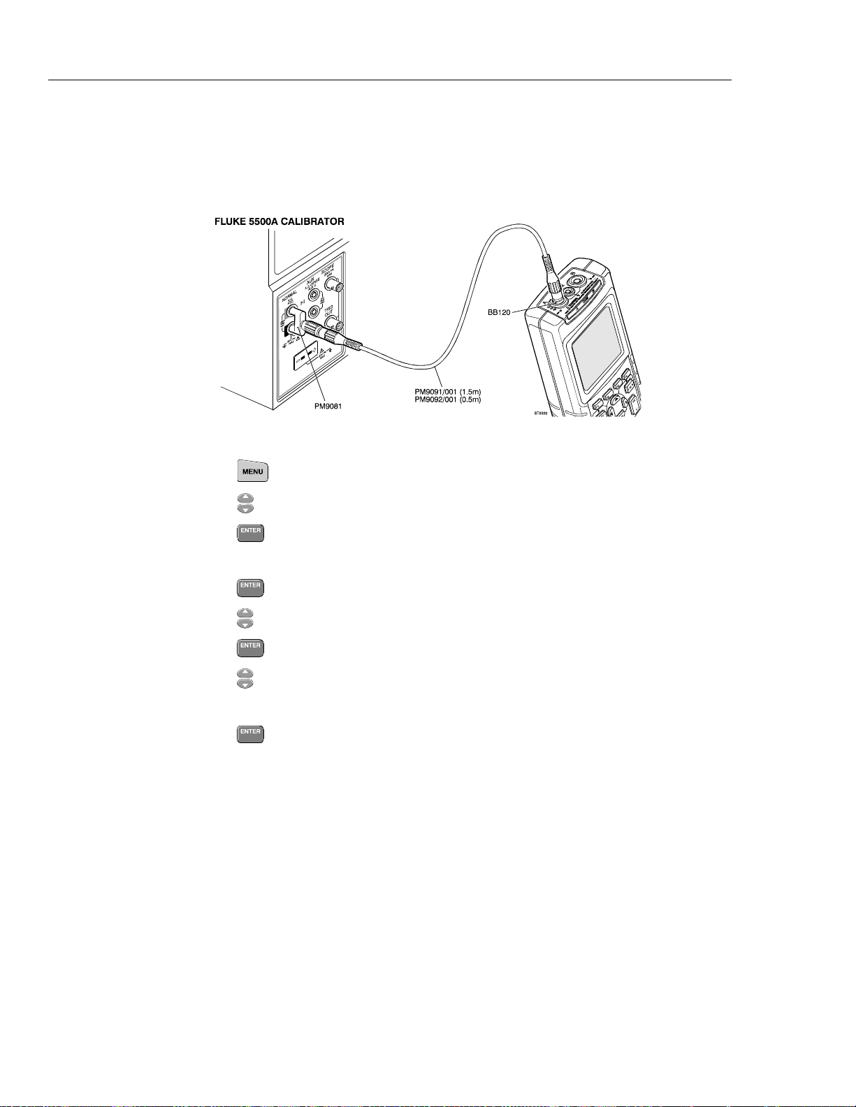
43B
Service Manual
4.12 Transients.
Proceed as follows to test the TRANSIENTS function:
1. Connect the test tool to the 5500A as show in Figure 4-12.
Figure 4-12. Test Tool Input 1 to 5500A Normal Output
ST8586.WMF
2. Press .
3. Press
4. Press
to highlight TRANSIENTS.
to select the TRANSIENTS mode.
VOLTAGE CHANGE will be highlighted, continue with:
1. Press
2. Press
3. Press
4. Press
.
to select 20%.
to confirm; mark changes to ■.
to select START.
5. Set the 5500A to 20V, 60Hz (NORMAL output, WAVE sine).
6. Press
to start the test. No transients should be captured.
7. Set the 5500A to 22.5V.
8. Now transients should be captured. After 40 transients (maximum) the 40th transient
will be visible.
9. When you are finished, set the 5500A to Standby.
4-32
Page 85

Chapter 5
Calibration Adjustment
Title Page
5.1 General ........................................................................................................ 5-3
5.1.1 Introduction.......................................................................................... 5-3
5.1.2 Calibration number and date................................................................ 5-3
5.1.3 General Instructions............................................................................. 5-4
5.2 Equipment Required For Calibration.......................................................... 5-4
5.3 Starting Calibration Adjustment ................................................................. 5-4
5.4 Contrast Calibration Adjustment ................................................................ 5-6
5.5 Warming Up & Pre-Calibration.................................................................. 5-7
5.6 Final Calibration ......................................................................................... 5-7
5.6.1 HF Gain Input 1. .................................................................................. 5-8
5.6.2 Delta T Gain, Trigger Delay Time & Pulse Adjust Input 1................. 5-9
5.6.3 Gain DMM (Gain Volt)....................................................................... 5-10
5.6.4 Volt Zero.............................................................................................. 5-12
5.6.5 Gain Ohm............................................................................................. 5-12
5.6.6 Capacitance Gain Low and High......................................................... 5-13
5.6.7 Capacitance Clamp & Zero.................................................................. 5-14
5.6.8 Capacitance Gain................................................................................. 5-14
5.7 Save Calibration Data and Exit................................................................... 5-15
5-1
Page 86

Page 87

5.1 General
5.1.1 Introduction
The following information, provides the complete Calibration Adjustment procedure for
the Fluke 43B test tool. The test tool allows closed-case calibration using known
reference sources. It measures the reference signals, calculates the correction factors,
and stores the correction factors in RAM. After completing the calibration, the
correction factors can be stored in FlashROM.
The test tool should be calibrated after repair, or if it fails the performance test. The test
tool has a normal calibration cycle of one year.
5.1.2 Calibration number and date
When storing valid calibration data in FlashROM after performing the calibration
adjustment procedure, the calibration date is set to the actual test tool date, and
calibration number is raised by one. To display the calibration date and - number:
Calibration Adjustment
5.1 General
5
1. Press
2. Press
3. Press
4. Press
5. Press
6. Press
7. Press
8. Press
to switch on the Fluke 43B.
to leave the startup screen.
to go to the MENU screen.
to highlight INSTRUMENT SETUP item.
to open the INSTRUMENT SETUP menu.
to highlight VERSION & CALIBRATION
to open the VERSION & CALIBRATION menu.
to return to the INSTRUMENT SETUP menu.
Figure 5-1. Version & Calibration Screen
VERSION.BMP
5-3
Page 88

43B
Service Manual
5.1.3 General Instructions
5.2 Equipment Required For Calibration
Follow these general instructions for all calibration steps:
• Allow the 5500A to satisfy its specified warm-up period. For each calibration point ,
wait for the 5500A to settle.
• The required warm up period for the test tool is included in the WarmingUp &
PreCal calibration step.
• Ensure that the test tool battery is charged sufficiently.
The primary source instrument used in the calibration procedures is the Fluke 5500A. If
a 5500A is not available, you can substitute another calibrator as long as it meets the
minimum test requirements.
• Fluke 5500A Multi Product Calibrator, including 5500A-SC Oscilloscope
Calibration Option.
• Stackable Test Leads (4x), supplied with the 5500A.
• 50Ω Coax Cables (2x), Fluke PM9091 or PM9092.
• 50Ω feed through termination (2x), Fluke PM9585.
• Fluke BB120 Shielded Banana to Female BNC adapters (2x), supplied with the
Fluke 43B.
• Dual Banana Plug to Female BNC Adapter (1x), Fluke PM9081/001.
• Male BNC to Dual Female BNC Adapter (1x), Fluke PM9093/001.
5.3 Starting Calibration Adjustment
Follow the steps below to start calibration adjustments.
1. Power the test tool via the power adapter input, using the PM8907 power adapter.
2. Check the actual test tool date, and adjust the date if necessary:
• Press
If the date on the startup screen is correct then continue at step 3.
• Press
• Press
• Press
• Press
• Press
• Press
• Adjust the date with
• When ready, press
to switch on the Fluke 43B.
to leave the STARTUP screen.
to go to MENU.
to highlight INSTRUMENT SETUP item.
to open the INSTRUMENT SETUP menu.
to highlight DATE
to open the DATE menu.
and if necessary.
.
5-4
• Press
3. Select the Maintenance mode.
to exit the INSTRUMENT SETUP menu.
Page 89

Calibration Adjustment
5.3 Starting Calibration Adjustment
The Calibration Adjustment Procedure uses built-in calibration setups, that can be
accessed in the Maintenance mode.
To enter the Maintenance mode proceed as follows:
5
• Press and hold
.
• Press and release .
• Release
.
• The display shows the Calibration Adjustment Screen.
The display shows the first calibration step
calibration status
:IDLE (valid) or :IDLE (invalid).
Warming Up (CL 0200) , and the
4. Continue with either a. or b. below:
a. To calibrate the display contrast adjustment range and the default contrast, go to
Section 5.4 Contrast Calibration Adjustment.
This calibration step is only required if the display cannot made dark or light
enough, or if the display after a test tool reset is too light or too dark
b. To calibrate the test tool without calibrating the contrast, go to Section 5.5
Warming Up & Pre-calibration
Explanation of screen messages and key functions.
When the test tool is in the Maintenance Mode, only the F1, F2, F3, and ENTER soft
keys, the ON/OFF key, and the backlight key can be operated, unless otherwise stated.
The calibration adjustment screen shows the actual calibration step (name and number)
and its status :
Cal Name (CL nnnn) :Status Calibration step nnnn
Status can be:
IDLE (valid) After (re)entering this step, the calibration process is not started.
The calibration data of this step are valid. This means that the
last time this step was done, the calibration process was
successful. It does not necessarily mean that the unit meets the
specifications related to this step!
IDLE (invalid) After (re)entering this step, the calibration process is not started.
The calibration data are invalid. This means that the unit will not
meet the specifications if the calibration data are saved.
BUSY aaa% bbb% Calibration adjustment step in progress; progress % for Input 1
and Input 2.
READY Calibration adjustment step finished.
Error :xxxx Calibration adjustment failed, due to wrong input signal(s) or
because the test tool is defective. The error codes xxxx are
shown for production purposes only.
5-5
Page 90

43B
Service Manual
5.4 Contrast Calibration Adjustment
Functions of the keys F1-ENTER are:
PREV select the previous step
NEXT select the next step
CAL start the calibration adjustment of the actual step
EXIT leave the Maintenance mode
Readings and traces
After completing a calibration step, readings and traces are shown using the new
calibration data.
After entering the Maintenance mode, the test tool display shows
Warming Up (CL 0200):IDLE (valid).
Do not press
now! If you did, turn the test tool off and on, and enter the
Maintenance mode again.
Proceed as follows to adjust the maximum display darkness (CL0100), the default
contrast (CL0110) , and the maximum display brightness (CL0120).
1. Press a three times to select the first calibration step. The display shows:
Contrast (CL 0100) :MANUAL
2. Press CAL. The display will show a dark test pattern, see Figure 5-2
3. Using
adjust the display to the maximum darkness, at which the test pattern is
only just visible.
4. Press to select the default contrast calibration. The display shows:
Contrast (CL 0110) :MANUAL
5. Press CAL. The display shows the test pattern at default contrast.
6. Using
7. Press to select maximum brightness calibration. The display shows:
Contrast (CL 0120) :MANUAL
set the display to optimal (becomes default) contrast.
8. Press CAL. The display shows a bright test pattern.
9. Using
adjust the display to the maximum brightness, at which the test pattern is
only just visible.
10. You can now :
• Exit, if only the Contrast had to be adjusted. Continue at Section 5.7.
OR
5-6
• Do the complete calibration. Press
and continue at Section 5.5.
to select the next step (Warming Up),
Page 91

Figure 5-2. Display Test Pattern
5.5 Warming Up & Pre-Calibration
After entering the Warming-Up & Pre-Calibration state, the display shows:
WarmingUp (CL 0200):IDLE (valid) or (invalid).
Calibration Adjustment
5.5 Warming Up & Pre-Calibration
5
You must always start the Warming Up & Pre Calibration at
Starting at another step will make the calibration invalid!
Proceed as follows:
1. Remove all input connections from the test tool.
2. Press
The display shows the calibration step in progress, and its status.
The first step is
counted down from 00:29:59 to 00:00:00. Then the other pre-calibration steps are
performed automatically. The procedure takes about 60 minutes.
3. Wait until the display shows End Precal :READY
4. Continue at Section 5.6.
to start the Warming-Up & Pre-Calibration.
WarmingUp (CL0200) :BUSY 00:29:59 . The warming-up period is
5.6 Final Calibration
You must always start the Final Calibration at the first step of Section 5.6.1. Starting at
another step will make the calibration invalid!
If you proceeded to step N (for example step CL 0615), then return to a previous step
(for example step CL 0613), and then calibrate this step, the complete final calibration
becomes invalid. You must do the final calibration from the beginning (step CL 0600)
again.
Warming Up (CL0200) .
You can repeat a step that shows the status
:READY by pressing again.
5-7
Page 92

43B
Service Manual
5.6.1 HF Gain Input 1.
Proceed as follows to do the HF Gain Input 1&2 calibration:
1. Press
to select the first calibration step in Table 5-1 ( HFG & FI AB (CL 0600): )
2. Connect the test tool to the 5500A as shown in Figure 5-3. Do NOT use a 50Ω
termination!
Figure 5-3. HF Gain Calibration Input Connections
3. Set the 5500A to source a 1 kHz fast rising edge square wave (Output SCOPE,
MODE edge) to the first calibration point in Table 5-1.
4. Set the 5500A in operate (OPR).
ST8097.WMF
5. Press
6. Wait until the display shows calibration status
7. Press
to start the calibration.
READY .
to select the next calibration step, set the 5500A to the next calibration
point, and start the calibration. Continue through all calibration points in Table 5-1.
8. Set the 5500A to source a 1 kHz square wave (Output SCOPE, MODE wavegen,
WAVE square), to the first calibration point in Table 5-2.
9. Press
10. Press
11. Wait until the display shows calibration status
12. Press
to select the first step in Table 5-2.
to start the calibration.
READY.
to select the next calibration step, set the 5500A to the next calibration
point, and start the calibration. Continue through all calibration points Table 5-2.
13. When you are finished, set the 5500A to Standby.
14. Continue at Section 5.6.2.
5-8
Page 93

Calibration Adjustment
Table 5-1. HF Gain Calibration Points Fast
Cal step 5500A Setting
(1 kHz, no 50 Ω!)
HFG & FI A(B) (CL 0600) 10 mV 20 mV
HFG & FI A(B) (CL 0601) 25 mV 50 mV
HFG & FI A(B) (CL 0602) 50 mV 100 mV
HFG & FI A(B) (CL 0603) 100 mV 200 mV
HFG & FI A(B) (CL 0604) 250 mV 500 mV
HFG & FI A(B) (CL 0605) 500 mV 1 V
HFG & FI A(B) (CL 0606) 1 V 2 V
1)
Test Tool Input Signal Requirements
(1 kHz, t
<100 ns, flatness after rising
rise
edge: <0.5% after 200 ns)
5.6 Final Calibration
1)
5
HFG & FI A(B) (CL 0607)
[HFG & FI A (CL 0608)]
1)
As the 5500A output is not terminated with 50Ω, its output voltage is two times its set voltage
2)
After starting the first step in this table cell, these steps are done automatically.
Cal step 5500A Setting
HF-Gain A(B) (CL 0609) 25 V 25 V
HF-Gain A (CL 0612),
[HF-Gain A (CL 0615)
1)
After starting the first step in this table cell, these steps are done automatically.
2)
Table 5-2. HF Gain Calibration Points Slow
(1 kHz, MODE wavegen,
1)
2.5 V 5 V
Test Tool Input Signal Requirements
(1 kHz square, t
WAVE square)
50 V 50 V
flatness after rising edge: <0.5% after 4 µs)
rise
5.6.2 Delta T Gain, Trigger Delay Time & Pulse Adjust Input 1
Proceed as follows to do the calibrations:
1. Press
2. Connect the test tool to the 5500A as shown in Figure 5-4.
to select calibration step Delta T (CL 0700):IDLE
<2 µs,
5-9
Page 94
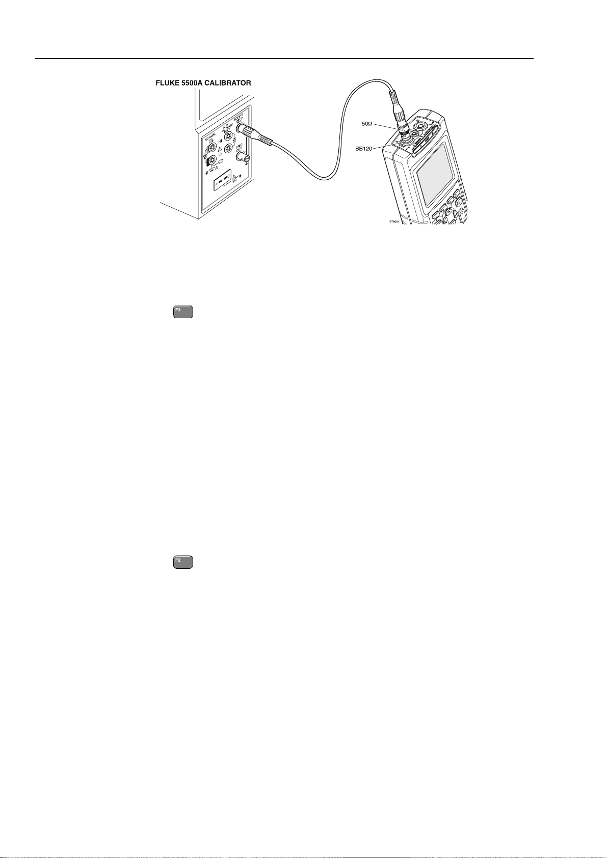
43B
Service Manual
Figure 5-4. 5500A Scope Output to Input 1
3. Set the 5500A to source a 1V, 1 MHz fast rising (rise time ≤ 1 ns) square wave
(SCOPE output, MODE edge).
4. Set the 5500A to operate (OPR).
5. Press
to start the calibration.
The Delta T gain, Trigger Delay (CL0720), and Pulse Adjust Input 1 (CL0640) will
be calibrated.
6. Wait until the display shows
7. When you are finished, set the 5500A to Standby.
8. Continue at Section 5.6.3.
5.6.3 Gain DMM (Gain Volt)
Dangerous voltages will be present on the calibration source
and connection cables during the following steps. Ensure that
the calibrator is in standby mode before making any connection
between the calibrator and the test tool.
ST8004.WMF
Pulse Adj A (CL 0640):READY.
Warning
5-10
Proceed as follows to do the Gain DMM calibration.
1. Press
to select the first calibration step in Table 5-3.
2. Connect the test tool to the 5500A as shown in Figure 5-5.
Page 95
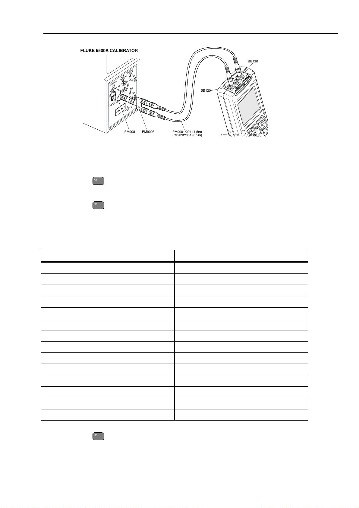
Calibration Adjustment
5.6 Final Calibration
5
Figure 5-5. Volt Gain Calibration Input Connections <300V
3. Set the 5500A to supply a DC voltage, to the first calibration point in Table 5-3.
4. Set the 5500A to operate (OPR).
5. Press
6. Wait until the display shows calibration status
7. Press
to start the calibration.
:READY.
to select the next calibration step, set the 5500A to the next calibration
point, and start the calibration. Continue through all calibration points of Table 5-3
8. Set the 5500A to Standby, and continue with step 9.
Table 5-3. Volt Gain Calibration Points <300V
Cal step Input value
Gain DMM (CL0800) 12.5 mV
Gain DMM (CL0801) 25 mV
Gain DMM (CL0802) 50 mV
Gain DMM (CL0803) 125 mV
Gain DMM (CL0804) 250 mV
ST8001.WMF
Gain DMM (CL0805) 500 mV
Gain DMM (CL0806) 1.25V
Gain DMM (CL0807) 2.5V
Gain DMM (CL0808) 5V
Gain DMM (CL0809) 12.5V
Gain DMM (CL0810) 25V
Gain DMM (CL0811) 50V (set 5500A to OPR!)
Gain DMM (CL0812) 125V
Gain DMM (CL0813) 250V
9. Press to select calibration step Gain DMM (CL0814) :IDLE
5-11
Page 96

43B
Service Manual
10. Connect the test tool to the 5500A as shown in Figure 5-6.
11. Set the 5500A to supply a DC voltage of 500V.
12. Set the 5500A to operate (OPR).
13. Press
Gain DMM (CL0814) and Gain DMM (CL0815) will be calibrated now.
14. Wait until the display shows calibration status
15. Set the 5500A to 0V (zero) and to Standby.
16. Continue at Section 5.6.4.
5.6.4 Volt Zero
Proceed as follows to do the Volt Zero calibration:
1. Press
2. Terminate Input 1 and Input 2 with the BB120 and a 50Ω or lower termination.
3. Press
4. Wait until the display shows
5. Remove the 50Ω termination from the inputs.
Figure 5-6. Volt Gain Calibration Input Connections 500V
ST8129.WMF
to start the calibration.
Gain DMM (CL0815):READY.
to select calibration adjustment step Volt Zero (CL 0820):IDLE.
to start the zero calibration of all mV/d settings (CL0820...CL0835)
Volt Zero (CL 0835):READY.
5-12
6. Continue at Section 5.6.5.
5.6.5 Gain Ohm
Proceed as follows to do the Gain Ohm calibration:
1. Press
2. Connect the UUT to the 5500A as shown in Figure 5-7.
Notice that the sense leads must be connected directly to the test tool.
to select calibration adjustment step Gain Ohm (CL 0860):IDLE
Page 97

Calibration Adjustment
5.6 Final Calibration
5
Figure 5-7. Four-wire Ohms calibration connections
3. Set the 5500A to the first test point in Table 5-4. Use the 5500A “COMP 2 wire”
mode for the calibration adjustments up to and including 100 kΩ. For the higher
values, the 5500A will turn off the “COMP 2 wire” mode.
4. Set the 5500A to operate (OPR).
5. Press
to start the calibration.
6. Wait until the display shows the calibration status
7. Press
to select the next calibration step, set the 5500A to the next calibration
point, and start the calibration. Continue through all calibration points.
8. When you are finished, set the 5500A to Standby.
9. Continue at Section 5.6.6.
Table 5-4. Ohm Gain Calibration Points
Cal Step Input Value
Gain Ohm (CL 0860) [Cap. Pos. (CL 0920), Cap.Neg. (CL 0921)]
Gain Ohm (CL 0861) [Cap. Pos. (CL 0922), Cap.Neg. (CL 0923)]
Gain Ohm (CL 0862) [Cap. Pos. (CL 0924), Cap.Neg. (CL 0925)]
Gain Ohm (CL 0863) [Cap. Pos. (CL 0926), Cap.Neg. (CL 0927)]
:READY.
1)
1)
1)
1)
ST8003.WMF
100 Ω
1 kΩ
10 kΩ
100 kΩ
Gain Ohm (CL 0864) 1 MΩ
Gain Ohm (CL 0865) [Gain Ohm (CL 0866)]
1)
The capacitance measurement current calibrations (Cap.Pos. and Cap.Neg) are done automatically after
the Gain Ohm calibration.
2)
The Gain Ohm (CL0866) calibration step is done automatically after the Gain Ohm (CL0865) calibration.
2)
10 MΩ
5.6.6 Capacitance Gain Low and High
Proceed as follows to do the Capacitance Gain calibration:
1. Press
2. Connect the test tool to the 5500A as shown in Figure 5-8.
to select calibration adjustment step Cap. Low (CL 0900):IDLE
5-13
Page 98

43B
Service Manual
Figure 5-8. Capacitance Gain Calibration Input Connections
3. Set the 5500A to supply 250 mV DC.
4. Set the 5500A to operate (OPR).
5. Press to start the calibration.
6. Wait until the display shows
7. Press
to select calibration adjustment step Cap. High (CL 0910):IDLE
8. Set the 5500A to supply 50 mV DC.
9. Press
to start the calibration.
10. Wait until the display shows
11. Set the 5500A to Standby.
12. Continue at Section 5.6.7.
5.6.7 Capacitance Clamp & Zero
Proceed as follows to do the Capacitance Clamp Voltage & Zero calibration:
1. Press
to select calibration adjustment step Cap. Clamp (CL 0940):IDLE
ST8002.WMF
Cap. Low (CL 0900):READY.
Cap High (CL 910):READY.
5-14
2. Remove any input connection from the test tool (open inputs).
3. Press
to start the calibration.
The capacitance measurement clamp voltage
the capacitance ranges
now.
4. Wait until the display shows
5. Continue at Section 5.6.8.
5.6.8 Capacitance Gain
Proceed as follows to do the Capacitance Gain calibration:
1. Press
2. Connect the test tool to the 5500A as shown in Figure 5-8.
3. Set the 5500A to 500 nF.
to select calibration adjustment step Cap. Gain (CL 0960):IDLE
Cap. Clamp (CL 0940), and the zero of
Cap. Zero (CL 0950)... Cap. Zero (CL 0953) will be calibrated
Cap. Zero (CL 0953): READY.
Page 99

4. Set the 5500A to operate (OPR).
Calibration Adjustment
5.7 Save Calibration Data and Exit
5
5. Press
6. Wait until the display shows
7. Continue at Section 5.7 to save the calibration data.
to start the calibration.
Cap. Gain (CL 0960):READY.
5.7 Save Calibration Data and Exit
Proceed as follows to save the calibration data, and to exit the Maintenance mode:
1. Remove all test leads from the test tool inputs.
2. Press (EXIT). The test tool will display:
Calibration data are valid
Save data and EXIT maintenance?
Note
Calibration data valid indicates that the calibration adjustment procedure
is performed correctly. It does not indicate that the test tool meets the
characteristics listed in Chapter 2.
3. Press
(YES) to save and exit.
Notes
The calibration number and date will be updated only if the calibration
data have been changed and the data are valid.
The calibration data will change when a calibration adjustment has been
done. The data will not change when just entering and then leaving the
maintenance mode without doing a calibration adjustment.
The calibration number and date will NOT be updated if only the display
contrast has been adjusted.
Possible error messages.
Invalid calibration data:
WARNING.Calibration data NOT valid.
Save data and EXIT?
Proceed as follows:
• To return to the Maintenance mode:
Press NO.
Now press
test tool, starting at Section 5.5.
until the display shows WarmingUp (CL 0200):IDLE, and calibrate the
5-15
Page 100
43B
Service Manual
• To exit and save the INVALID calibration data:
Press
The test tool will show the message
your service center at power on. The calibration date and number will not be
YES.
The test tool needs calibration. Please contact
updated. A complete recalibration must be done.
• To exit and maintain the old calibration data:
Turn the test tool off.
No power adapter voltage
WARNING.No adapter present.
Calibration data will not be saved.
Exit maintenance mode?
• To save the calibration data:
Press
NO
The test tool returns to the maintenance mode. Connect a correct power adapter,
and press
to exit and save.
• To exit without saving the calibration data:
Press
YES
5-16
 Loading...