Fairchild Semiconductor MOC8204 Datasheet

DESCRIPTION
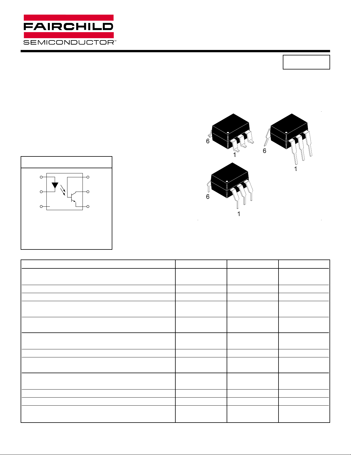
The MOC8204 device consists of a gallium arsenide infrared emitting diode
optically coupled to a high voltage, silicon, phototransistor detector in a
standard 6-pin DIP package. It is designed for high voltage applications and
is particularly useful in copy machines and solid state relays.
GENERAL PURPOSE 6-PIN
PHOTOTRANSISTOR OPTOCOUPLERS
MOC8204
APPLICATIONS
• Copy Machines
• Interfacing and coupling systems of different potentials and impedances
• Monitor and Detection Circuits
• Solid State Relays
Parameter Symbol Value Units
TOTAL DEVICE
T
STG
-55 to +150 °C
Storage Temperature
Operating Temperature T
OPR
-55 to +100 °C
Lead Solder Temperature T
SOL
260 for 10 sec °C
Input-Output Isolation Voltage
V
ISO
7500 Vac(pk)
Peak ac Voltage, 60 Hz, 1 Second Duration
(1)
Total Device Power Dissipation @ TA= 25°C
P
D
250
mW
Derate above 25°C 2.94
EMITTER
I
F
60 mA
DC/Average Forward Input Current
Forward Current - Peak (Pulse Width = 1µs, 330 pps) IF(pk) 1.2 A
LED Power Dissipation @ TA= 25°C
P
D
120 mW
Derate above 25°C 1.41 mW/°C
DETECTOR
V
CEO
400 V
Collector-Emitter Voltage
Collector-Base Voltage V
CBO
400 V
Emitter-Collector Voltage V
ECO
7V
Detector Power Dissipation @ TA= 25°C
P
D
150 mW
Derate above 25°C 1.76 mW/°C
SCHEMATIC
2001 Fairchild Semiconductor Corporation
DS300269 3/22/01 1 OF 6 www.fairchildsemi.com
1
2
3NC
PIN 1. ANODE
2. CATHODE
3. NO CONNECTION
4. EMITTER
5. COLLECTOR
6. BASE
6
5
4

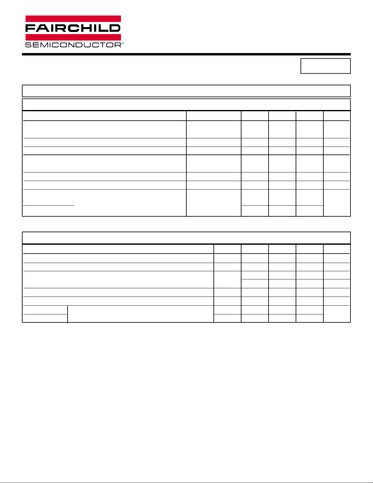
Parameter Test Conditions Symbol Min Typ
(1)
Max Unit
EMITTER
(I
F
= 10 mA) V
F
— 1.2 15 V
Input Forward Voltage
Reverse Leakage Current (VR= 6.0 V) I
R
——
10 µA
Capacitance (V = 0, f =1 MHz) C
J
—
18
—
pF
DETECTOR
BV
CEO
400 — — V
Collector-Emitter Breakdown Voltage (I
C
= 1.0 mA, RBE= 1M!)
Collector-Base Breakdown Voltage (IC= 100 µA) BV
CBO
400
——
V
Emitter-Base Breakdown Voltage (IE= 100 µA) BV
EBO
7
——
V
Collector-Emitter Dark Current
T
A
= 25°C (RBE= 1M!, VCE= 300 V) I
CEO
— — 100
nA
T
A
= 100
°C
— — 250
µA
INDIVIDUAL COMPONENT CHARACTERISTICS
ELECTRICAL CHARACTERISTICS
(TA= 25°CUnless otherwise specified.)
Notes
1. Alway design to the specified minimum/maximum electrical limits (where applicable).
2. Current Transfer Ratio (CTR) = IC/IFx 100%.
3. For this test LED pins 1 and 2 are common and phototransistor Pins 4,5 and 6 are common.
GENERAL PURPOSE 6-PIN
PHOTOTRANSISTOR OPTOCOUPLERS
Characteristic Test Conditions Symbol Min Typ
(1)
Max Units
Output Collector Current (VCE= 10 V, IF= 10 mA, RBE= 1M!)IC (CTR)
(2)
2 (20)
— — mA(%)
Collector-Emitter Saturation Voltage (IC= 0.5 mA, IF= 10 mA, RBE= 1M!)V
(SAT)
—
—
0.4 V
Input-Output Isolation Voltage
(3)
(I
I-O
≤ 1 µA, Time = 1min) V
ISO
5300
——
V
AC(RMS)
7300
——
V
AC(PEAK)
Isolation Resistance
(3)
R
ISO
—
10
11
—
!
Isolation Capacitance
(1)
C
ISO
0.2 pf
Turn-On Time
(V
CC
= 10 V, IC= 2 mA, RL= 100!)
t
ON
—5—
µs
Turn-Off Time t
OFF
—5—
ISOLATION CHARACTERISTICS
MOC8204
www.fairchildsemi.com 2 OF 6 3/22/01 DS300269
 Loading...